Embed Size (px)
Citation preview
Resources:Science news story.Word bank.Activity 1: Mixed-up meanings.Activity 2: Comprehension.Activity 3: Find the missing word.Activity 4: What kind of statements?Activity 5: Topic for group discussion or pupil presentations. Links to free activities, lesson plans and background information.Daily tip for running science class discussions and groupwork.
NewsManchester: 28-Feb-2007, Eurekalert.
Size zero materialsResearchers have used the world’s thinnest material to create the world’s smallest transistor. It’s a breakthrough that could spark the development of a new type of super-fast computer chip.
real science

Professor Andre Geim and Dr Kostya Novoselov are at the School of Physics and Astronomy at the University of Manchester. They reveal details of transistors that are only one atom thick and less than 50 atoms wide in the March issue of Nature Materials.
The scientists believe this innovation will allow the miniaturisation of electronics to continue when the current silicon-based technology runs out of steam.
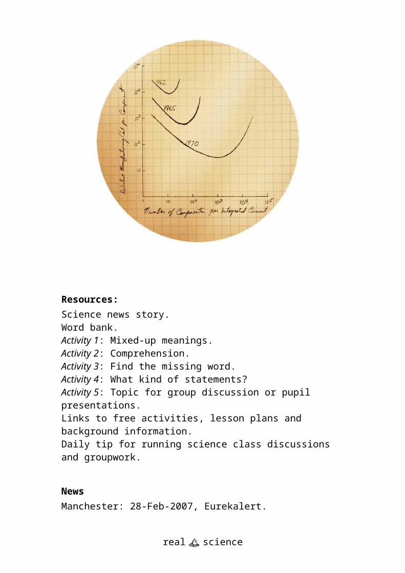
In recent decades, manufacturers have crammed more and more components onto integrated circuits. As a result, the number of transistors and the power of these circuits have doubled roughly every two years. This is known as Moore’s Law.
But the speed of cramming is now slowing. Further miniaturisation of electronics will face its most fundamental challenge in the next 10 years or so.
Two years ago, Professor Andre Geim and his team discovered a new class of materials. These can be thought of as individual atomic planes pulled out of bulk crystals. These one-atom-thick materials have rapidly become one of the hottest topics in physics. Graphene – a gauze of carbon atoms like chicken-wire – is particularly interesting.
The first graphene-based transistor was reported by the University of Manchester team at the same time as the discovery of graphene. Other groups have recently reproduced the result.
But these graphene transistors were very ‘leaky’. This ruled out important applications with a high density of transistors. These include computer chips.
Now the Manchester team has found an elegant way around the problem. They have made graphene-based transistors suitable for use in future computer chips.
Professor Geim and his team have shown for the first time that graphene remains stable and conductive when it is cut into strips only a few nanometres wide.
All other known materials oxidise and become unstable at sizes tens times larger.
real science
This poor stability has been the fundamental barrier to future electronic devices. This in turn threatens to limit the future development of microelectronics.
The team has made ribbons just a few nanometres wide, says Professor Geim. “We cannot rule out the possibility of confining graphene even further – down to maybe a single ring of carbon atoms.”
Future electronic circuits could be carved out of a single graphene sheet. Geim’s team have proved this idea by making a number of single-electron-transistor devices that work under ambient conditions. They show a high-quality transistor action.
At present no technology can cut individual elements with nanometre precision, says Dr Leonid Ponomarenko, who is leading this research at the University of Manchester. “We have to rely on chance by narrowing our ribbons to a few nanometres in width. Some were too wide and did not work properly. Others were over-cut and broken."
But Dr Ponomarenko is hopeful that this proof-of-concept technique can be scaled up.
Making transistors at nanometre scale is the same challenge that modern silicon-based technology is facing now, he said. That technology has progressed steadily from millimetre-sized transistors to the microprocessors in today’s devices. These have individual parts that are tens of nanometres in size.
“The next logical step is true nanometre-sized circuits. This is where graphene can come into play because it remains stable – unlike silicon or other materials – even at these dimensions.”
Professor Geim does not expect that graphene-based circuits will come of age before 2025. Until then, silicon technology should remain dominant.
But he believes graphene may be the only approach that will work after the silicon era comes to an end.
The material combines many attractive features from other technologies, he said.
“Graphene combines most exciting features from carbon-nanotube, single-electron and molecular electronics, all in one.”
real science

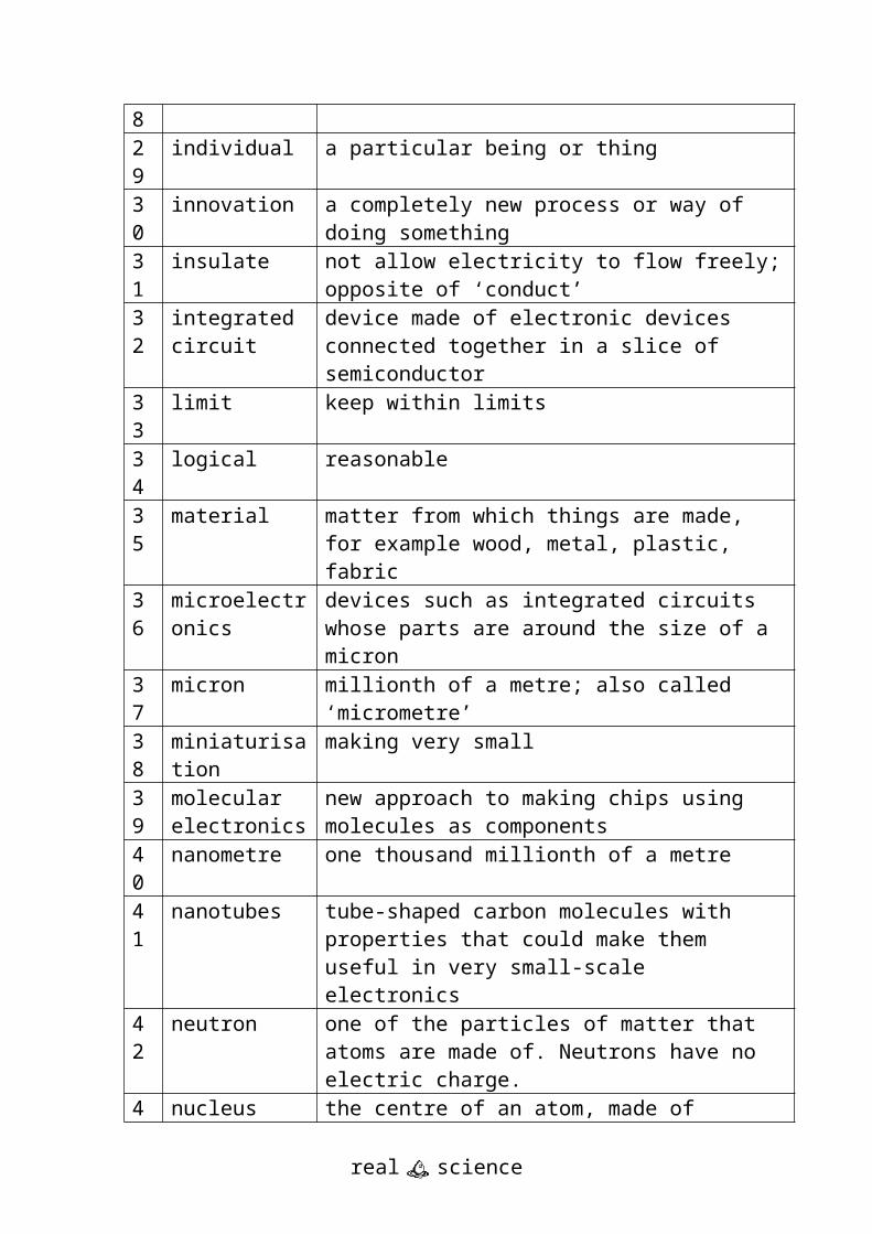
The research of Professor Geim, Dr Kostya Novoselov and colleagues at the University of Manchester led to the discovery of a new class of materials called two-dimensional atomic crystals back in 2004. Professor Geim was recently awarded the 2007 Mott Medal and Prize by The Institute of Physics for his discovery of graphene and his 'remarkable contribution' to science.
625 wordsFlesch reading ease: 47.3Flesch-Kincaid Grade level: 10.
real science
Word bankPupils will not know some of the words used in the text. Meanings are given below, followed by an exercise in matching words and meanings.
Teachers may choose to provide some or all of the meanings to help pupils read and understand the story. An approach that leads to better learning is to ask pupils to complete as much of Activity 1 as possible during their first encounter with the text.
By tackling this exercise and those that follow – which are known collectively as directed activities related to texts (DARTs) – pupils can engage with a piece of writing, and learn a great deal from it, even when many of its ideas and words are unfamiliar to them.
Word Meaning1 ambient surrounding2 application way of putting to use3 atom smallest unit of an element, made of protons and
neutrons in a nucleus surrounded by electrons4 attract draw towards5 barrier something that prevents a thing from happening6 bulk large mass or shape7 challenge new and exciting but difficult task8 chip integrated circuit 9 circuit arrangement of components through which electricity
can flow10 component one of the parts something is made of11 concept general idea12 conduct allow electricity to flow freely through it13 conductive letting electricity flow freely through it14 confining keeping within limits15 crystal a solid made of atoms or molecules arranged in regular
patterns. Crystals have straight edges and flat surfaces.16 density number per unit volume17 device something made for a special purpose18 dimensions size; length, breadth and height19 dominant strongest; most powerful20 electric charge property of particle of matter that means it is attracted
or repelled by other particles21 electric current flow of electric charge
real science
22 electron one of the particles of matter that atoms are made of. Electrons have a negative electric charge.
23 electronic to do with the flow of electrons24 electronics devices that work by a flow of electrons25 elegant simple but clever and pleasing26 element substance that cannot be split by chemistry into simpler
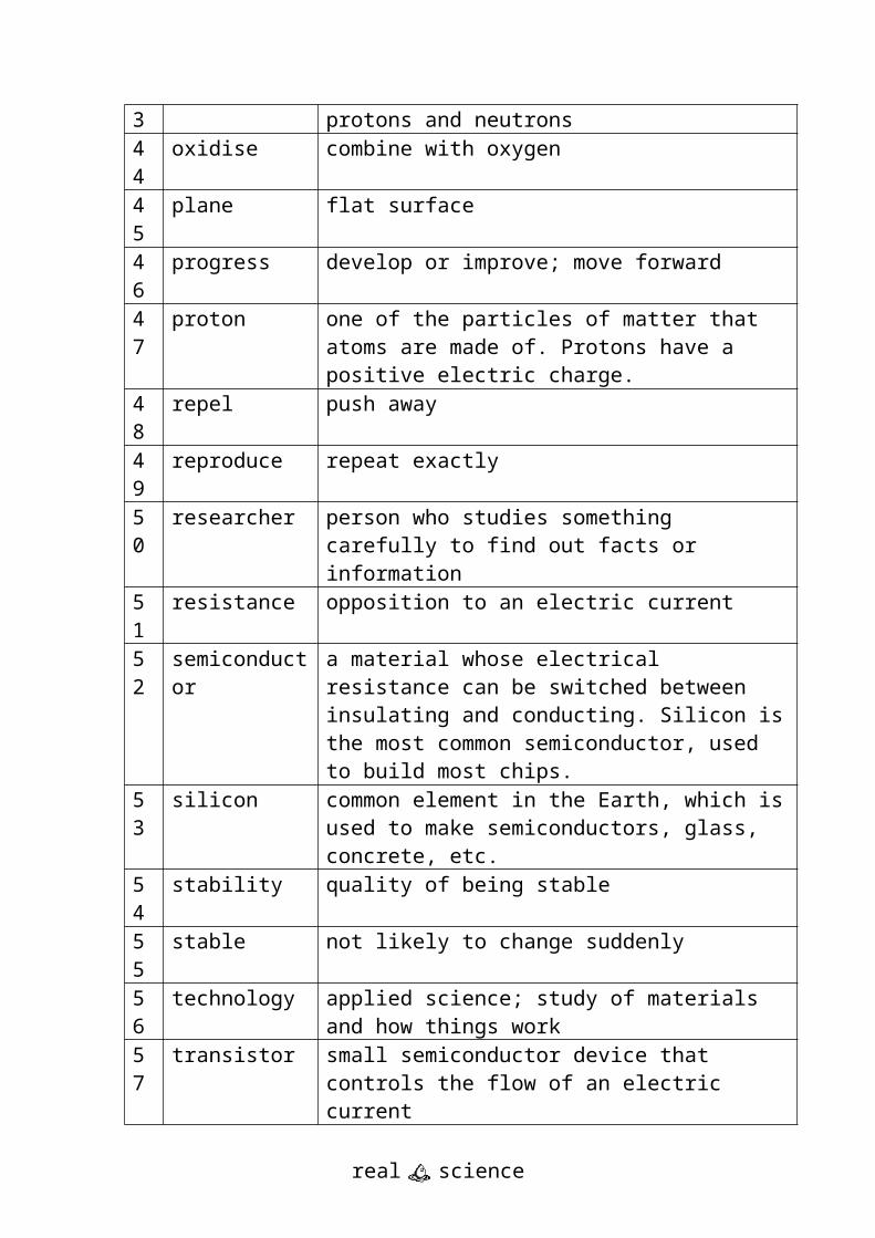
substances27 fundamental basic and essential28 gauze fine mesh29 individual a particular being or thing30 innovation a completely new process or way of doing something31 insulate not allow electricity to flow freely; opposite of
‘conduct’32 integrated
circuitdevice made of electronic devices connected together in a slice of semiconductor
33 limit keep within limits34 logical reasonable35 material matter from which things are made, for example wood,
metal, plastic, fabric36 microelectronics devices such as integrated circuits whose parts are
around the size of a micron37 micron millionth of a metre; also called ‘micrometre’38 miniaturisation making very small39 molecular
electronicsnew approach to making chips using molecules as components
40 nanometre one thousand millionth of a metre41 nanotubes tube-shaped carbon molecules with properties that
could make them useful in very small-scale electronics42 neutron one of the particles of matter that atoms are made of.
Neutrons have no electric charge.43 nucleus the centre of an atom, made of protons and neutrons44 oxidise combine with oxygen45 plane flat surface46 progress develop or improve; move forward47 proton one of the particles of matter that atoms are made of.
Protons have a positive electric charge.48 repel push away49 reproduce repeat exactly50 researcher person who studies something carefully to find out facts
or information51 resistance opposition to an electric current 52 semiconductor a material whose electrical resistance can be switched
real science

between insulating and conducting. Silicon is the most common semiconductor, used to build most chips.
53 silicon common element in the Earth, which is used to make semiconductors, glass, concrete, etc.
54 stability quality of being stable55 stable not likely to change suddenly56 technology applied science; study of materials and how things work57 transistor small semiconductor device that controls the flow of an
electric current58 unstable not stable
real science
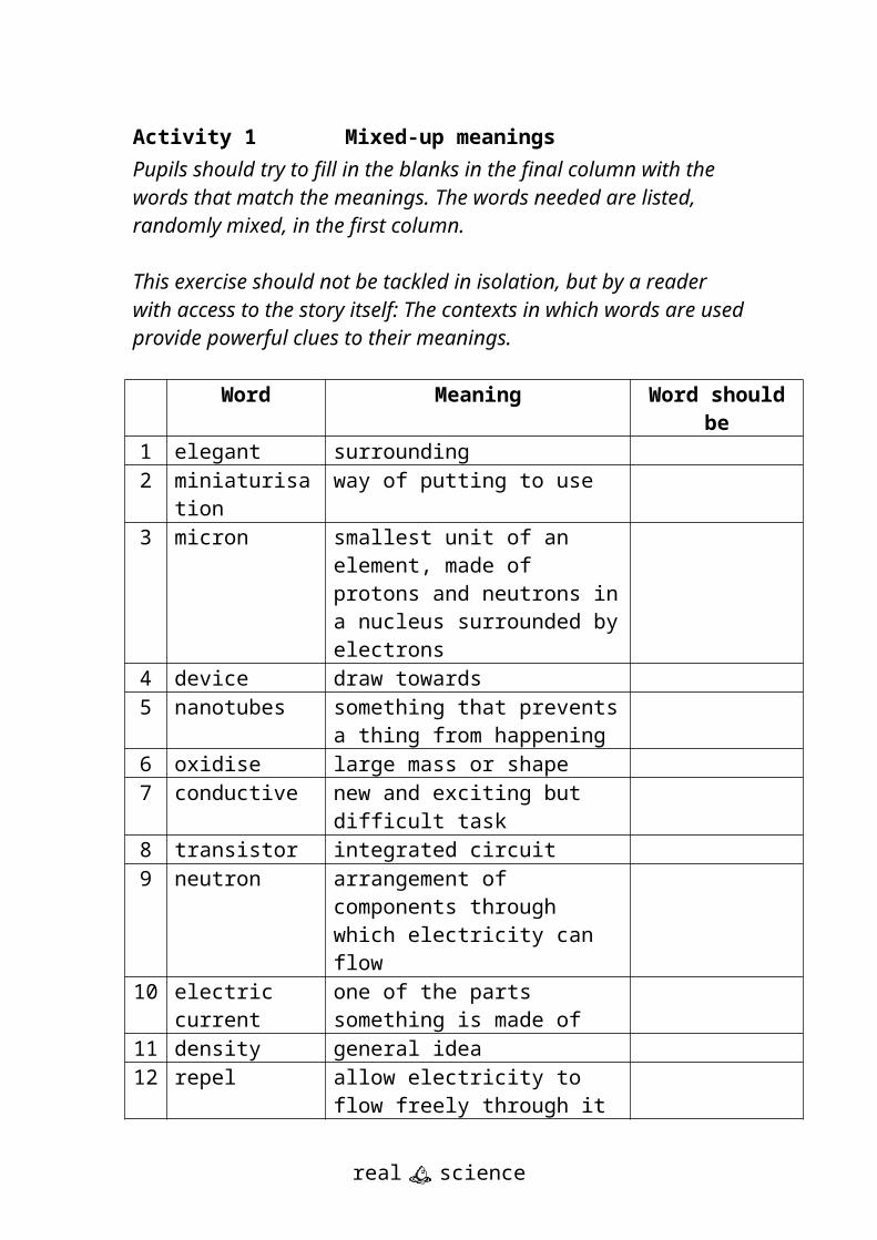
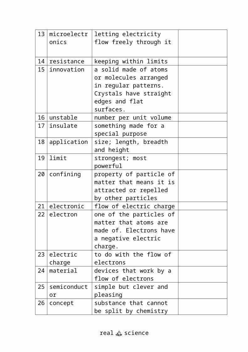
Activity 1 Mixed-up meaningsPupils should try to fill in the blanks in the final column with the words that match the meanings. The words needed are listed, randomly mixed, in the first column.
This exercise should not be tackled in isolation, but by a reader with access to the story itself: The contexts in which words are used provide powerful clues to their meanings.
Word Meaning Word should be1 elegant surrounding2 miniaturisation way of putting to use3 micron smallest unit of an element, made
of protons and neutrons in a nucleus surrounded by electrons
4 device draw towards5 nanotubes something that prevents a thing
from happening6 oxidise large mass or shape7 conductive new and exciting but difficult task8 transistor integrated circuit 9 neutron arrangement of components
through which electricity can flow10 electric current one of the parts something is made
of11 density general idea12 repel allow electricity to flow freely
through it13 microelectronics letting electricity flow freely
through it14 resistance keeping within limits15 innovation a solid made of atoms or
molecules arranged in regular patterns. Crystals have straight edges and flat surfaces.
16 unstable number per unit volume17 insulate something made for a special
purpose18 application size; length, breadth and height19 limit strongest; most powerful20 confining property of particle of matter that
real science
means it is attracted or repelled by other particles
21 electronic flow of electric charge22 electron one of the particles of matter that
atoms are made of. Electrons have a negative electric charge.
23 electric charge to do with the flow of electrons24 material devices that work by a flow of
electrons25 semiconductor simple but clever and pleasing26 concept substance that cannot be split by
chemistry into simpler substances27 progress basic and essential28 dominant fine mesh29 dimensions a particular being or thing30 ambient a completely new process or way
of doing something31 researcher not allow electricity to flow freely;
opposite of ‘conduct’32 barrier device made of electronic devices
connected together in a slice of semiconductor
33 crystal keep within limits34 reproduce reasonable35 proton matter from which things are
made, for example wood, metal, plastic, fabric
36 gauze devices such as integrated circuits whose parts are around the size of a micron
37 chip millionth of a metre; also called ‘micrometre’
38 integrated circuit making very small39 logical new approach to making chips
using molecules as components40 stable one thousand millionth of a metre41 technology tube-shaped carbon molecules
with properties that could make them useful in very small-scale electronics
42 electronics one of the particles of matter that atoms are made of. Neutrons have
real science

no electric charge.43 nanometre the centre of an atom, made of
protons and neutrons44 circuit combine with oxygen45 nucleus flat surface46 individual develop or improve; move forward47 fundamental one of the particles of matter that
atoms are made of. Protons have a positive electric charge.
48 challenge push away49 component repeat exactly50 bulk person who studies something
carefully to find out facts or information
51 silicon opposition to an electric current 52 attract a material whose electrical
resistance can be switched between insulating and conducting. Silicon is the most common semiconductor, used to build most chips.
53 atom common element in the Earth, which is used to make semiconductors, glass, concrete, etc.
54 stability quality of being stable55 element not likely to change suddenly56 conduct applied science; study of materials
and how things work57 molecular
electronicssmall semiconductor device that controls the flow of an electric current
58 plane not stable
real science
Activity 2 Comprehension 1. What is special about the material the scientists have used?
2. What have they made with it?
3. How thick are the devices they have made?
4. What is Moore’s Law?
5. What is happening to Moore’s Law?
6. In your own words what does “fundamental challenge” mean?
7. In what way is the “new class of materials” Prof Geim discovered two years ago different from ordinary materials?
8. What element is graphene made from?
9. What was wrong with the original graphene transistors?
10.How does graphene behave when it is just a few nanometres wide?
11.How do all other known materials behave when they are cut as thin as this?
12.So because graphene remains stable when cut very small it can be used to make smaller electronic circuits than can be made with silicon. There is still a problem however – what is that?
13.Do the scientists believe this can be solved?
14.What words in the story help answer the last question?
15.Silicon technology began with millimetre sized transistors. These are now down to nanometre size on silicon chips. A millimetre is a thousandth of a metre, while a nanometre is a billionth of a metre. So by what factor have transistors been shrunk – ten, a thousand or a million?
16.Is Moore’s Law a real law of science, such as Newton’s laws of motion or the law of gravitation?
real science
17.Is it a law at all?
18.Briefly explain your thinking behind the last answer you gave.
real science
Activity 3 Find the missing wordPupils should try to fill in the blanks using clues from the rest of the sentence. When in doubt, the length of each blank indicates the length of the missing word. A complete list of words that belong in the blanks is provided at the end of the passage.
Size zero materialsResearchers have used the world's thinnest material __ create the world's smallest transistor. It's a breakthrough that _____ spark the development of a new type of super-fast ________ chip.
Professor Andre Geim and Dr Kostya Novoselov are at ___ School of Physics and Astronomy at the University of __________. They reveal details of transistors that are only ___ atom thick and less than 50 atoms wide in ___ March issue of Nature Materials.
The scientists believe this innovation ____ allow the miniaturization of electronics to continue when the _______ silicon-based technology runs out of steam.
In recent decades, manufacturers ____ crammed more and more components onto integrated circuits. As _ result, the number of transistors and the power of _____ circuits have doubled roughly every two years. This is _____ as Moore's Law.
But the speed of cramming is now _______. Further miniaturization of electronics will face its most ___________ challenge in the next 10 years or so.
Two years ___, Professor Andre Geim and his team discovered a ___ class of materials. These can be thought of as __________ atomic planes pulled out of bulk crystals. These one-atom-thick _________ have rapidly become one of the hottest topics in _______. Graphene - a gauze of carbon atoms like ____________ - is particularly interesting.
The first graphene-based transistor was reported __ the University of Manchester team at the same time __ the discovery of graphene. Other groups have recently reproduced ___ result .
real science
But these graphene transistors were very 'leaky'. This _____ out important applications with a high density of transistors. _____ include computer chips.
Now the Manchester team has found an _______ way around the problem. They have made graphene-based transistors ________ for use in future computer chips.
Professor Geim and his ____ have shown for the first time that graphene remains ______ and conductive when it is cut into strips only _ few nanometres wide.
All other known materials oxidise and become ________ at sizes tens times larger.
This poor stability has been ___ fundamental barrier to future electronic devices. This in turn _________ to limit the future development of microelectronics.
The team has ____ ribbons just a few nanometres wide, says Professor Geim. ___ cannot rule out the possibility of confining graphene even _______ - down to maybe a single ring of carbon _____."
Future electronic circuits could be carved out of a ______ graphene sheet. Geim's team have proved this idea by ______ a number of single-electron-transistor devices that work under ambient __________. They show a high-quality transistor action.
At present no __________ can cut individual elements with nanometre precision, says Dr ______ Ponomarenko, who is leading this research at the University __ Manchester. "We have to rely on chance by narrowing ___ ribbons to a few nanometres in width. Some were ___ wide and did not work properly. Others were over-cut ___ broken."
But Dr Ponomarenko is hopeful that this proof-of-concept technique ___ be scaled up.
Making transistors at nanometre scale is the ____ challenge that modern silicon-based technology is facing now, he ____. That technology has progressed steadily from millimetre-sized transistors __ the microprocessors in today's devices. These have individual _____ that are tens of nanometres in size.
real science
"The next logical ____ is true nanometre-sized circuits. This is where graphene can ____ into play because it remains stable - unlike silicon __ other materials - even at these dimensions."
Professor Geim does ___ expect that graphene-based circuits will come of age before ____. Until then, silicon technology should remain dominant.
But he ________ graphene may be the only approach that will work _____ the silicon era comes to an end.
The material combines ____ attractive features from other technologies, he said.
"Graphene combines most ________ features from carbon-nanotube, single-electron and molecular electronics, all in ___."
These are all the words that belong in the blanks:2025, “We, a, a, after, ago, and, as, atoms, believes, by, can, chicken-wire, come, computer, conditions, could, current, elegant, exciting, fundamental, further, have, individual, known, Leonid, made, making, Manchester, many, materials, new, not, of, one, one, or, our, parts, physics, ruled, said, same, single, slowing, stable, step, suitable, team, technology, the, the, the, the, these, These, threatens, to, to, too, unstable, will
real science
Answer Key:
Size zero materialsResearchers have used the world's thinnest material to create the world's smallest transistor. It's a breakthrough that could spark the development of a new type of super-fast computer chip.
Professor Andre Geim and Dr Kostya Novoselov are at the School of Physics and Astronomy at the University of Manchester. They reveal details of transistors that are only one atom thick and less than 50 atoms wide in the March issue of Nature Materials.
The scientists believe this innovation will allow the miniaturization of electronics to continue when the current silicon-based technology runs out of steam.
In recent decades, manufacturers have crammed more and more components onto integrated circuits. As a result, the number of transistors and the power of these circuits have doubled roughly every two years. This is known as Moore's Law.
But the speed of cramming is now slowing. Further miniaturization of electronics will face its most fundamental challenge in the next 10 years or so.
Two years ago, Professor Andre Geim and his team discovered a new class of materials. These can be thought of as individual atomic planes pulled out of bulk crystals. These one-atom-thick materials have rapidly become one of the hottest topics in physics. Graphene - a gauze of carbon atoms like chicken-wire - is particularly interesting.
The first graphene-based transistor was reported by The University of Manchester team at the same time as the discovery of graphene. Other groups have recently reproduced the result.
But these graphene transistors were very 'leaky'. This ruled out important applications with a high density of transistors. These include computer chips.
real science
Now the Manchester team has found an elegant way around the problem. They have made graphene-based transistors suitable for use in future computer chips.
Professor Geim and his team have shown for the first time that graphene remains stable and conductive when it is cut into strips only a few nanometres wide.
All other known materials oxidise and become unstable at sizes tens times larger.
This poor stability has been the fundamental barrier to future electronic devices. This in turn threatens to limit the future development of microelectronics.
The team has made ribbons just a few nanometres wide, says Professor Geim. "We cannot rule out the possibility of confining graphene even further - down to maybe a single ring of carbon atoms."
Future electronic circuits could be carved out of a single graphene sheet. Geim's team have proved this idea by making a number of single-electron-transistor devices that work under ambient conditions. They show a high-quality transistor action.
At present no technology can cut individual elements with nanometre precision, says Dr Leonid Ponomarenko, who is leading this research at the University of Manchester. "We have to rely on chance by narrowing our ribbons to a few nanometres in width. Some were too wide and did not work properly. Others were over-cut and broken."
But Dr Ponomarenko is hopeful that this proof-of-concept technique can be scaled up.
Making transistors at nanometre scale is the same challenge that modern silicon-based technology is facing now, he said. That technology has progressed steadily from millimetre-sized transistors to the microprocessors in today's devices. These have individual parts that are tens of nanometres in size.
"The next logical step is true nanometre-sized circuits. This is where graphene can come into play because it remains stable - unlike silicon or other materials - even at these dimensions."
real science

Professor Geim does not expect that graphene-based circuits will come of age before 2025. Until then, silicon technology should remain dominant.
But he believes graphene may be the only approach that will work after the silicon era comes to an end.
The material combines many attractive features from other technologies, he said.
"Graphene combines most exciting features from carbon-nanotube, single-electron and molecular electronics, all in one."
real science
Activity 4 What kind of statement?Students should read the news story on page 1 about the latest scientific research, and highlight phrases or sentences according to the following key (or any other way of indicating the different types of statement that can be done with the resources in their pockets or in your classroom):
Existing knowledgeReasons/aims for doing the researchTechnology and methodsNew findings or developmentsHypothesisPredictionEvidenceIssues and applicationsIssues and applications
Normally no more than one phrase or sentence should be highlighted in each paragraph, unless the reader decides that a particular paragraph contains several really important ideas.
Usually the decision will not be too difficult. But choosing between, say, hypotheses and new findings can sometimes be tricky. There isn’t always an obviously right or wrong answer, even to the scientists themselves.
Pupils should be encouraged not to agonise too long over their choice of statement type, but to be prepared to give reasons for their decisions.
Note: A hypothesis is a “tentative explanation that leads to predictions that can be tested by experiment or observation”.
Answer Key: (This is an illustrative set of choices. There are many others.)
Size zero materialsResearchers have used the world’s thinnest material to create the world’s smallest transistor. It’s a breakthrough that could spark the development of a new type of super-fast computer chipa new type of super-fast computer chip.
Professor Andre Geim and Dr Kostya Novoselov are at the School of Physics and Astronomy at the University of Manchester. They reveal
real science
details of transistors that are only one atom thick and less than 50 atoms wide in the March issue of Nature Materials.
The scientists believe this innovation will allow the miniaturisation of miniaturisation of electronics to continue electronics to continue when the current silicon-based technology runs out of steam.
In recent decades, manufacturers have crammed more and more components onto integrated circuits. As a result, the number of transistors and the power of these circuits have doubled roughly every two years. This is known as Moore’s Law.
But the speed of cramming is now slowing. Further miniaturisation of electronics will face its most fundamental challenge in the next 10 years or so.
Two years ago, Professor Andre Geim and his team discovered a new class of materials. These can be thought of as individual atomic planes pulled out of bulk crystals. These one-atom-thick materials have rapidly become one of the hottest topics in physics. Graphene – a gauze of carbon atoms like chicken-wire – is particularly interesting.
The first graphene-based transistor was reported by the University of Manchester team at the same time as the discovery of graphene. Other groups have recently reproduced the result.
But these graphene transistors were very ‘leaky’. This ruled out important applications with a high density of transistors. These include computer chips.
Now the Manchester team has found an elegant way around the problem. They have made graphene-based transistors suitable for use in future computer chips.
Professor Geim and his team have shown for the first time that graphene remains stable and conductive when it is cut into strips only a few nanometres wide.
All other known materials oxidise and become unstable at sizes tens times larger.
real science
This poor stability has been the fundamental barrier to future the fundamental barrier to future electronic deviceselectronic devices. This in turn threatens to limit the future development of microelectronics.
The team has made ribbons just a few nanometres wide, says Professor Geim. “We cannot rule out the possibility of confining graphene even further – down to maybe a single ring of carbon atomsdown to maybe a single ring of carbon atoms.”
Future electronic circuits could be carved out of a single graphene Future electronic circuits could be carved out of a single graphene sheetsheet. Geim’s team have proved this idea by making a number of single-electron-transistor devices that work under ambient conditions. They show a high-quality transistor action.
At present no technology can cut individual elements with nanometre precision, says Dr Leonid Ponomarenko, who is leading this research at the University of Manchester. “We have to rely on chance by narrowing our ribbons to a few nanometres in width. Some were too wide and did not work properly. Others were over-cut and broken."
But Dr Ponomarenko is hopeful that this proof-of-concept technique can be scaled up.
Making transistors at nanometre scaleMaking transistors at nanometre scale is the same challenge that modern silicon-based technology is facing now, he said. That technology has progressed steadily from millimetre-sized transistors to the microprocessors in today’s devices. These have individual parts that are tens of nanometres in size.
“The next logical step is true nanometre-sized circuitsnext logical step is true nanometre-sized circuits. This is where graphene can come into play because it remains stable – unlike silicon or other materials – even at these dimensions.”
Professor Geim does not expect that graphene-based circuits will come of age before 2025. Until then, silicon technology should remain dominant.
But he believes graphene may be the only approach that will work after the silicon era comes to an end.
The material combines many attractive features from other technologies, he said.
“Graphene combines most exciting features from carbon-nanotube, single-electron and molecular electronics, all in one.”
real science
Activity 5 Topics for group discussion or pupil presentationsCarbon is the most versatile element in the periodic table. It is the foundation of organic chemistry and is the basic element in plant and animal cells. It is an essential component of plastics and many pharmaceuticals.
Divide the class into three groups. Assign each group one of the sets of carbon compounds below to research. When they have completed their research, have each student group make a poster and present what they learned to the class.
Group 1: Diamonds, coal, graphite
Group 2: Oil, natural gas, plastics, pharmaceuticals
Group 3: Proteins, fats, carbohydrates
As an extension, ask students to research how or why carbon can exist in such dramatically different forms, colours, and characteristics. (Carbon has four bonding positions in its outer electron shell and is unique in its ability to form double and triple bonds. Carbon can form incredibly complex chain molecules, rings, sheets, lattices, buckyballs, and tube structures. There are more types of compounds formed with carbon than with any other element.)
Adapted from Nova.
Links to free activities, resources and lessons1. http://www.pbs.org/transistor/album1/moore/index.html “When
Gordon Moore began working at Shockley Semiconductor in 1956, he barely knew what a semiconductor was. Within ten years he was well on his way to being one of the greatest visionaries of the semiconductor world.” Includes audio of Moore talking about the impact of the transistor.
2. http://www.pbs.org/transistor/index.html "The Transistor was probably the most important invention of the 20th Century, and the story behind the invention is one of clashing egos and top secret research." Portal to lots of good stuff for teachers and pupils. For example:
real science

3. http://www.pbs.org/transistor/teach/teach.html “To help students better understand the transistor and its impact on technology, the documentary and website are accompanied by this Teachers' Guide… The Teachers' Guide includes a range of activities, appropriate for middle-school or high-school use, plus a series of profiles of young scientists and their work.
4. http://www.intel.com/museum/archives/history_docs/mooreslaw.htm All about Moore’s Law. From Intel.
5. http://www.teachersdomain.org/resources/phy03/sci/phys/matter/ metal/index.html “This interactive activity from NOVA describes the crystalline structure of metal and uses animations to illustrate the molecular changes that occur when a metallic substance is bent, heated, or otherwise changed by external forces.”
6. http://www.manchester.ac.uk/aboutus/news/pressreleases/einstein/ “Einstein's relativity theory proven with the 'lead' of a pencil.” Earlier press release about graphene.
7. http://www.manchester.ac.uk/press/newsarchive/title,4655,en.htm “Researchers have discovered the world's first single-atom-thick fabric, which reveals the existence of a new class of materials and may lead to computers made from a single molecule.” Original discovery of graphene.
8. http://gtresearchnews.gatech.edu/newsrelease/graphene.htm “Graphite, the material that gives pencils their marking ability, could be the basis for a new class of nanometre-scale electronic devices that have the attractive properties of carbon nanotubes – but could be produced using established microelectronics manufacturing techniques.”
9. http://www.eurekalert.org/pub_releases/2006-10/uom-pst101906.php “Graphene is a single layer of carbon atoms densely packed in a honeycomb crystal lattice. The material is made from splitting graphite apart into individual atomic planes, through a process similar to tracing with a pencil. The resulting atomic sheet is unexpectedly stable, highly flexible and strong, and very conductive.” Earlier press release about Graphene.
10.http://www.engr.sjsu.edu/WofMatE/Structure.htm “The structure of a material may be divided into four levels: atomic structure, atomic
real science

arrangement, microstructure, and macrostructure.” Page on crystal structures with nice pics and links.
11.http://www.swansea.ac.uk/mateng/what/main.htm “Materials science and engineering : ‘never heard of it’ is a common enough response both from students at school as well as from the general public. Compared to other science and engineering subjects, it can be a bit of a mystery… However, it is a vitally important subject, underlying all the others and playing a key role in developments in science and technology… most major technological advances throughout history have only been possible through a better understanding and use of materials.”
Links to more linkshttp://www.pbs.org/transistor/photocredits.html Transistorized!http://www.photon.t.u-tokyo.ac.jp/~maruyama/agallery/agallery.html Animation gallery of nanotubes, fullerenes etc.
Daily tip for science class discussions and groupworkSome 40,000 students passed through Ohio State’s introductory biology courses during the five years that Rissing directed the university’s introductory biology program. While he’s no longer the director, the students still follow the curriculum he helped establish.
The majority of students taking these courses aren’t science majors and, in theory, may have very little interest in sitting in a biology classroom.
“So we liberated the non-majors curriculum,” Rissing said. “In most cases, instructors tended to teach watered-down biology to students taking these introductory classes.”
The curriculum for non-majors now focuses on the implication of “big picture” issues. Students enrolled in these courses are often required to read the New York Times each day and be ready to discuss science-related issues that make headlines.
“My job isn’t to prepare these students for med school,” Rissing said. “My job is to help the students attain a level of scientific literacy so that they can contribute to a serious discussion on these larger issues.”
real science
Rissing pointed out that scientific literacy rates in the United States have risen to 16 percent, up from 9 percent about a decade ago. He attributes that in part to changing how students, and ultimately their teachers, are taught.
“The most crucial players in fostering scientific literacy are the K-12 science teachers, but we teach those teachers in college,” Rissing said. “The college professors and scientists are ultimately the ones that foster public understanding and opinions of science.”
From a press release on the methods of Steve Rissing, a biology professor at Ohio State University. “Rissing played a major role in revamping the way the university teaches its introductory-level biology courses.”
real science