Embed Size (px)
Citation preview

Chili2S Module DatasheetRev. 0.5, September 2019
GENERAL DESCRIPTIONThe Chili2S module is a fully-featured Thread-certified wirelessmodule solution for IEEE 802.15.4 communications in the2.4GHz band. It pairs the Cascoda CA-8211 SMARTRange™transceiver modem with the Nuvoton M2351 Cortex®-M23TrustZone® microcontroller.
With industry leading power consumption and sensitivityperformance, it delivers unparalleled range without externalamplifier components, thus providing whole-house connectivityin any market on the planet.
FEATURES● SMARTRange™ CA-8211 IEEE 802.15.4 modem
◦ Thread-certified component for every role
◦ Industry-leading receive sensitivity of -105dBm
◦ Programmable transmit power of -3dBm to +9dBm
◦ Industry-leading link budget of 114dB
◦ Integrated MAC low-power co-processor
● NuMicro® M2351 TrustZone® MCU
◦ Arm® Cortex®-M23 Architecture
◦ Highly robust security for IoT applications
◦ 512 KB dual-bank application ROM (APROM) for Over-The-Air (OTA) upgrade
◦ 96 KB on-chip SRAM
◦ Communication interfaces (UART, I2C, SPI, USB)
◦ Analog Interfaces (ADC, DAC, Comp)
◦ Smart Card (ISO 7816) and SD Card Interfaces
● World-class energy consumption
◦ World’s best receiver efficiency
14mA (42mW) at -105dBm sensitivity (0.0316nW)
Figure of Merit (FoM) 0.75 (mW*nW)-1
◦ 19mA at +9dBm transmit power
◦ 3µA sleep mode
● Industrial temperature range: -40°C to +85°C
● Wide supply voltage range: 2.1V to 3.6V
● Chip antenna and all other RF components integrated onmodule
● 16 MHz crystal for system clock and 32.768 kHz crystal forlow-power RTC functionality
● Module size: 27.00 x 21.05 mm
DEVELOPMENT TOOLS● Certified Thread stack based on OpenThread
● Optimised interface for the M2351 MCU and the CA8211hardware MAC
● Module can be detached node running the network stack andapplication or coprocessor for hosts running Linux within aThread mesh network
● Cascoda SDK, making full use of CMake as a build system
● Code available open-source on GitHub
BENEFITSEquipment cost: Increased range removes the need forexternal power amplifiers, thereby reducing component BOM.
Installation cost: Greater datalink reliability lessens the needfor skilled installers, and the consumer can self-install.
Maintenance cost: Lower power consumption means thatbatteries last longer, thereby minimising maintenance cost.
Development time: Use of pre-certified module minimisesproduct development time.
APPLICATIONS● Home and building automation
● Consumer electronics
● Lighting systems
● Heating, ventilation & air-conditioning systems (HVAC)
● Smart grid (AMI/AMR)
● Asset tracking (active RFID)
● Industrial control and monitoring
● Assisted living & telecare
Protected by Patents US 8849226, US 9660692 1 www.cascoda.comand corresponding rights in other territories

Chili2S Module Datasheet, Rev. 0.5
Table of Contents 1 Overview...................................................................................................................................................................... 3 2 Hardware Description................................................................................................................................................... 4
2.1 Module Pin Configuration........................................................................................................................................................... 4 2.2 Recommended Footprint............................................................................................................................................................ 5 2.3 Pin Descriptions......................................................................................................................................................................... 6 2.4 Multi-Function Pin (MFP) Mapping.............................................................................................................................................7 2.5 JTAG/SWD ICE Connector for Programming and Debug..........................................................................................................8 2.6 Power Supply............................................................................................................................................................................. 8 2.7 RF Circuitry................................................................................................................................................................................ 8
3 Electrical Specification................................................................................................................................................. 9 3.1 Absolute Maximum Ratings........................................................................................................................................................ 9 3.2 Environmental Conditions.......................................................................................................................................................... 9 3.3 Recommended Operating Conditions........................................................................................................................................9 3.4 Digital Pin Characteristics.......................................................................................................................................................... 9 3.5 Supply Currents.......................................................................................................................................................................... 9 3.6 General RF Characteristics...................................................................................................................................................... 10 3.7 Receiver RF Characteristics..................................................................................................................................................... 10 3.8 Transmitter RF Characteristics.................................................................................................................................................10
4 Software Support....................................................................................................................................................... 11 5 Regulatory Approvals ................................................................................................................................................ 12 6 Soldering Information................................................................................................................................................. 12 7 References................................................................................................................................................................. 12 8 Revision History......................................................................................................................................................... 12
Protected by Patents US 8849226, US 9660692 2 www.cascoda.com
Chili2S Module Datasheet, Rev. 0.5
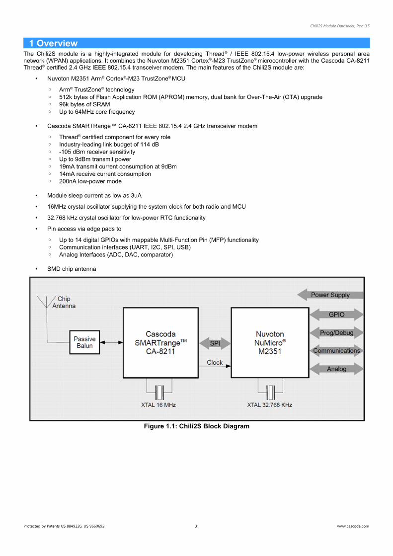
1 OverviewThe Chili2S module is a highly-integrated module for developing Thread® / IEEE 802.15.4 low-power wireless personal areanetwork (WPAN) applications. It combines the Nuvoton M2351 Cortex®-M23 TrustZone® microcontroller with the Cascoda CA-8211Thread® certified 2.4 GHz IEEE 802.15.4 transceiver modem. The main features of the Chili2S module are:
• Nuvoton M2351 Arm® Cortex®-M23 TrustZone® MCU
◦ Arm® TrustZone® technology◦ 512k bytes of Flash Application ROM (APROM) memory, dual bank for Over-The-Air (OTA) upgrade◦ 96k bytes of SRAM◦ Up to 64MHz core frequency
• Cascoda SMARTRange™ CA-8211 IEEE 802.15.4 2.4 GHz transceiver modem
◦ Thread® certified component for every role◦ Industry-leading link budget of 114 dB◦ -105 dBm receiver sensitivity◦ Up to 9dBm transmit power◦ 19mA transmit current consumption at 9dBm◦ 14mA receive current consumption◦ 200nA low-power mode
• Module sleep current as low as 3uA
• 16MHz crystal oscillator supplying the system clock for both radio and MCU
• 32.768 kHz crystal oscillator for low-power RTC functionality
• Pin access via edge pads to
◦ Up to 14 digital GPIOs with mappable Multi-Function Pin (MFP) functionality◦ Communication interfaces (UART, I2C, SPI, USB)◦ Analog Interfaces (ADC, DAC, comparator)
• SMD chip antenna
Figure 1.1: Chili2S Block Diagram
Protected by Patents US 8849226, US 9660692 3 www.cascoda.com

Chili2S Module Datasheet, Rev. 0.5
2 Hardware Description
2.1 Module Pin ConfigurationThe following figure shows the front view of the Chili2S module. The edge pads (Pin1 to Pin42) for solder-down are on 1.27mmpitch.
Protected by Patents US 8849226, US 9660692 4 www.cascoda.com
Figure 2.1: Chili2S Module Front View (Unit:mm)
Chili2S Module Datasheet, Rev. 0.5
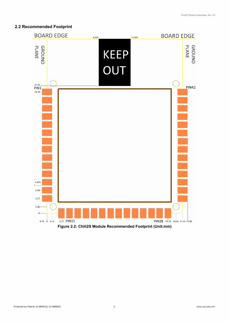
2.2 Recommended Footprint
Protected by Patents US 8849226, US 9660692 5 www.cascoda.com
Figure 2.2: Chili2S Module Recommended Footprint (Unit:mm)

Chili2S Module Datasheet, Rev. 0.5
2.3 Pin Descriptions
Pin Name Type M2351 Port Description1 VDD33 Supply - 3.3V Power Supply
2 TMS GPIO PF.0 ICE/JLINK Data
3 GND Ground - Module Ground
4 TCK GPIO PF.1 ICE/JLINK Clock
5 PB.12 GPIO PB.12 General Purpose Digital I/O
6 PB.13 GPIO PB.13 General Purpose Digital I/O
7 - GPIO PB.14 NC1)
8 - GPIO PC.1 NC1)
9 - GPIO PC.0 NC1)
10 TRSTX3) Digital In - System Reset and ICE/JLINK Reset (active low)
11 PA.13 GPIO PA.13 General Purpose Digital I/O
12 PA.14 GPIO PA.14 General Purpose Digital I/O
13 VDD33 Supply - 3.3V Power Supply
14 GND Ground - Module Ground
15 PA.15 GPIO PA.15 General Purpose Digital I/O
16 GND Ground - Module Ground
17 PA.12 GPIO PA.12 General Purpose Digital I/O
18 GND Ground - Module Ground
19 GND Ground - Module Ground
20 GND Ground - Module Ground
21 GND Ground - Module Ground
22 GND Ground - Module Ground
23 GND Ground - Module Ground
24 GND Ground - Module Ground
25 GND Ground - Module Ground
26 AVDD33 Supply - Filtered 3.3V Supply2)
27 GND Ground - Module Ground
28 VDD33 Supply - 3.3V Power Supply
29 - - - NC1)
30 GND Ground - Module Ground
31 PB.5 GPIO PB.5 General Purpose Digital I/O
32 PB.4 GPIO PB.4 General Purpose Digital I/O
33 PB.3 GPIO PB.3 General Purpose Digital I/O
34 PB.2 GPIO PB.2 General Purpose Digital I/O
35 PB.1 GPIO PB.1 General Purpose Digital I/O
36 PB.0 GPIO PB.0 General Purpose Digital I/O
37 - GPIO PF.5 NC1)
38 - GPIO PF.4 NC1)
39 - GPIO PA.3 NC1)
40 - GPIO PA.0 NC1)
41 - GPIO PA.2 NC1)
42 - GPIO PA.1 NC1)
Table 2.1: Chili2S Module Pin Descriptions
Notes:
1) NC: Do not connect, as pin is internally connected on module.
2) AVDD33 is a filtered supply output generated by the module for noise-sensitive peripherals. Do not connect to VDD33.
3) TRSTX (Pin 10) can be used by an external host to reset the Chili2S module. Leave unconnected if not used.
Protected by Patents US 8849226, US 9660692 6 www.cascoda.com
Chili2S Module Datasheet, Rev. 0.5
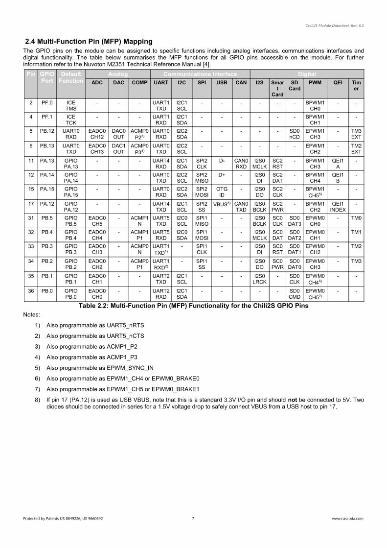
2.4 Multi-Function Pin (MFP) MappingThe GPIO pins on the module can be assigned to specific functions including analog interfaces, communications interfaces anddigital functionality. The table below summarises the MFP functions for all GPIO pins accessible on the module. For furtherinformation refer to the Nuvoton M2351 Technical Reference Manual [4].
Pin GPIOPort
DefaultFunction
Analog Communications Interface Digital
ADC DAC COMP UART I2C SPI USB CAN I2S Smart
Card
SDCard
PWM QEI Timer
2 PF.0 ICETMS
- - - UART1TXD
I2C1SCL
- - - - - - BPWM1CH0
- -
4 PF.1 ICETCK
- - - UART1RXD
I2C1SDA
- - - - - - BPWM1CH1
- -
5 PB.12 UART0RXD
EADC0CH12
DAC0OUT
ACMP0P23)
UART0RXD
I2C2SDA
- - - - - SD0nCD
EPWM1CH3
- TM3EXT
6 PB.13 UART0TXD
EADC0CH13
DAC1OUT
ACMP0P34)
UART0TXD
I2C2SCL
- - - - - - EPWM1CH2
- TM2EXT
11 PA.13 GPIOPA.13
- - - UART4RXD
I2C1SDA
SPI2CLK
D- CAN0RXD
I2S0MCLK
SC2RST
- BPWM1CH3
QEI1A
-
12 PA.14 GPIOPA.14
- - - UART0TXD
I2C2SCL
SPI2MISO
D+ - I2S0DI
SC2DAT
- BPWM1CH4
QEI1B
-
15 PA.15 GPIOPA.15
- - - UART0RXD
I2C2SDA
SPI2MOSI
OTGID
- I2S0DO
SC2CLK
- BPWM1CH55)
- -
17 PA.12 GPIOPA.12
- - - UART4TXD
I2C1SCL
SPI2SS
VBUS8) CAN0TXD
I2S0BCLK
SC2PWR
- BPWM1CH2
QEI1INDEX
-
31 PB.5 GPIOPB.5
EADC0CH5
- ACMP1N
UART5TXD
I2C0SCL
SPI1MISO
- - I2S0BCLK
SC0CLK
SD0DAT3
EPWM0CH0
- TM0
32 PB.4 GPIOPB.4
EADC0CH4
- ACMP1P1
UART5RXD
I2C0SDA
SPI1MOSI
- - I2S0MCLK
SC0DAT
SD0DAT2
EPWM0CH1
- TM1
33 PB.3 GPIOPB.3
EADC0CH3
- ACMP0N
UART1TXD1)
- SPI1CLK
- - I2S0DI
SC0RST
SD0DAT1
EPWM0CH2
- TM2
34 PB.2 GPIOPB.2
EADC0CH2
- ACMP0P1
UART1RXD2)
- SPI1SS
- - I2S0DO
SC0PWR
SD0DAT0
EPWM0CH3
- TM3
35 PB.1 GPIOPB.1
EADC0CH1
- - UART2TXD
I2C1SCL
- - - I2S0LRCK
- SD0CLK
EPWM0CH46)
- -
36 PB.0 GPIOPB.0
EADC0CH0
- - UART2RXD
I2C1SDA
- - - - - SD0CMD
EPWM0CH57)
- -
Table 2.2: Multi-Function Pin (MFP) Functionality for the Chili2S GPIO PinsNotes:
1) Also programmable as UART5_nRTS
2) Also programmable as UART5_nCTS
3) Also programmable as ACMP1_P2
4) Also programmable as ACMP1_P3
5) Also programmable as EPWM_SYNC_IN
6) Also programmable as EPWM1_CH4 or EPWM0_BRAKE0
7) Also programmable as EPWM1_CH5 or EPWM0_BRAKE1
8) If pin 17 (PA.12) is used as USB VBUS, note that this is a standard 3.3V I/O pin and should not be connected to 5V. Twodiodes should be connected in series for a 1.5V voltage drop to safely connect VBUS from a USB host to pin 17.
Protected by Patents US 8849226, US 9660692 7 www.cascoda.com

Chili2S Module Datasheet, Rev. 0.5
2.5 JTAG/SWD ICE Connector for Programming and DebugA footprint is supplied on the bottom side of the module for a 10-pin connector to directly connect a programmer or debugginginterface, for example a Segger J-Link Debug Probe.
Figure 2.3: 10-Pin Header for JTAG/ICE Programming and Debug
Note that the Pinout in Figure 2.3 shows the module bottom side view and is therefore mirrored compared to the footprint indicationon the top left of Figure 2.1.
Note that all JTAG/SWD signals can also be accessed via the edge pads of the module.
2.6 Power SupplyAll VDD33 pins (pins 1, 13 and 28) are connected to the same net on the module, therefore only one connection is required tosupply the module. It is however recommended to connect as many as VDD33 pins as possible to decrease impedance for thepower connections. No additional external components such as supply filters are required.
AVDD33 is a filtered version of VDD33 used both on the module and connected to pin 26 as analog power output, so it can be usedto supply noise-sensitive off-module peripherals. It should not be connected to VDD33.
2.7 RF CircuitryThe Chili2S module uses a passive balun design for impedance matching and converting the differential signal of the CA-8211 to asingle-ended 50Ω signal for connecting the SMD chip antenna.
When mounting the Chili2S module onto a host board, the module top edge should be aligned with the board edge with the antennafacing out, see Figure 2.2. To maximise range, an adequate ground plane must be provided on the host PCB. Correctly positioned,the ground plane on the host PCB will contribute significantly to the antenna performance. The area around and under the antenna,marked KEEP OUT, must be kept clear of conductors or other metal objects on any layer of the host board.
Protected by Patents US 8849226, US 9660692 8 www.cascoda.com
12
34
56
78
910
VDD33
GND
GND
GND
GND
TMS
TCK
NC
NC
TRSTX

Chili2S Module Datasheet, Rev. 0.5
3 Electrical SpecificationThis section specifies important parameters for the Chili2S module. For more detailed information refer to the Nuvoton M2351Datasheet [3] and the Cascoda CA-8211 Datasheet [2].
3.1 Absolute Maximum Ratings
Parameter Conditions Min Typ Max Units
Voltage (on any pin) -0.3 - 3.9 V
Storage Temperature Range -65 - 150 °C
Input RF Level - - +10 dBm
Table 3.1: Absolute Maximum RatingsStresses beyond those listed under “Absolute Maximum Ratings” may cause permanent damage to the module. These are stressratings only, and functional operation of the device at these or any other conditions beyond those indicated in the operationalsections of the specification is not implied. Exposure to absolute maximum rating conditions for extended periods may affect devicereliability.
3.2 Environmental Conditions
Parameter Conditions Min Typ Max Units
ESD Human-body model, JEDEC STD 22 - - 2000 V
Charged-device model, JEDEC STD 22 - - 500 V
MSL MSL3
Table 3.2: Environmental Conditions
3.3 Recommended Operating Conditions
Parameter Min Typ Max Units
Operating Supply Voltage – Device Supply (VDD33) 2.1 - 3.6 V
Operating Temperature -40 - 85 °C
Table 3.3: Recommended Operating Conditions
3.4 Digital Pin Characteristics
Parameter Symbol Conditions Min Typ Max Units
Input Low Voltage (TTL Input) VIL VDD33=3.3V - - 0.8 V
Input High Voltage (TTL Input) VIH VDD33=3.3V 2.0 - - V
Pull-up Resistor RPU - 53 - kΩ
Input Leakage Current @ VI=3.3V II - - 1 uA
Output Sink Current IOL VDD33=3.3V, Vin=VSS+0.4V 3.6 - 19.9 mA
Output Source Current IOH VDD33=3.3V, Vin=VDD33-0.4V -20.6 - -3.4 mA
Table 3.4: Digital Pin Characteristics
3.5 Supply CurrentsSpecified for VDD33=3.3V, T=25'C, System Clock=16MHz.
Parameter Symbol Conditions Min Typ Max Units
Transmit IDDTx Tx Power +9 dBmTx Power 0 dBm
2013
mAmA
Receive IDDRx -105 dBm Sensitivity 15 mA
Processor active, Radio Off IDDACTIVE 1.5 mA
Sleep Mode IDDSLEEP 3 uA
Table 3.5: Supply Currents
Protected by Patents US 8849226, US 9660692 9 www.cascoda.com
Chili2S Module Datasheet, Rev. 0.5
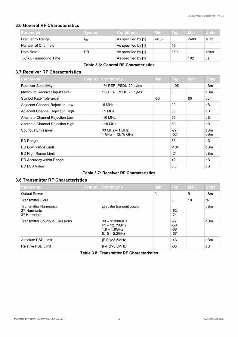
3.6 General RF Characteristics
Parameter Symbol Conditions Min Typ Max Units
Frequency Range IFR As specified by [1] 2405 2480 MHz
Number of Channels As specified by [1] 16
Data Rate DR As specified by [1] 250 kbit/s
TX/RX Turnaround Time As specified by [1] 192 μs
Table 3.6: General RF Characteristics
3.7 Receiver RF Characteristics
Parameter Symbol Conditions Min Typ Max Units
Receiver Sensitivity 1% PER, PSDU 20 bytes -105 dBm
Maximum Receiver Input Level 1% PER, PSDU 20 bytes 0 dBm
Symbol Rate Tolerance -80 80 ppm
Adjacent Channel Rejection Low -5 MHz 22 dB
Adjacent Channel Rejection High +5 MHz 35 dB
Alternate Channel Rejection Low -10 MHz 50 dB
Alternate Channel Rejection High +10 MHz 50 dB
Spurious Emissions 30 MHz – 1 GHz1 GHz – 12.75 GHz
-77-52
dBmdBm
ED Range 83 dB
ED Low Range Limit -104 dBm
ED High Range Limit -21 dBm
ED Accuracy within Range ±2 dB
ED LSB Value 0.5 dB
Table 3.7: Receiver RF Characteristics
3.8 Transmitter RF Characteristics
Parameter Symbol Conditions Min Typ Max Units
Output Power 0 9 dBm
Transmitter EVM 5 10 %
Transmitter Harmonics2nd Harmonic3rd Harmonic
@9dBm transmit power-52-74
dBm
Transmitter Spurious Emissions 30 – ≤1000MHz>1 – 12.75GHz1.8 – 1.9GHz5.15 – 5.3GHz
-77-50-68-67
dBm
Absolute PSD Limit |F-Fc|>3.5MHz -43 dBm
Relative PSD Limit |F-Fc|>3.5MHz -35 dB
Table 3.8: Transmitter RF Characteristics
Protected by Patents US 8849226, US 9660692 10 www.cascoda.com

Chili2S Module Datasheet, Rev. 0.5
4 Software SupportThe Cascoda open-source Software Development Kit (SDK) is available on GitHub (https://github.com/Cascoda/cascoda-sdk) andcontains the API, drivers and interfaces required for developing applications using OpenThread or custom IEEE 802-15-4 basednetwork connectivity.
The Cascoda SDK kit for the Chili2S module and the Nuvoton M2351 MCU contains:
● Optimised and exhaustively tested MAC-level (MCPS/MLME) API and interface drivers
● Hardware-MAC interface and configuration for OpenThread, an open-source implementation of the Thread® IPv6 based wireless mesh networking stack (https://openthread.io/)
● Example library for sensor interface drivers
● Low power modes
● Examples for custom IEEE 802.15.4 MAC based applications
● Hardware abstraction functions for module I/O handling , timers etc.
Build Environment
The Cascoda SDK makes full use of CMake as a build system, to enable advanced configuration and cross-platform developmentin combination with the ARM® GCC compiler toolchain. Build environments for other embedded compilers (IAR, Keil) are alsoavailable.
Protected by Patents US 8849226, US 9660692 11 www.cascoda.com
Chili2S Module Datasheet, Rev. 0.5
5 Regulatory Approvals EC, FCC and ISED certification and modular approval is in progress.
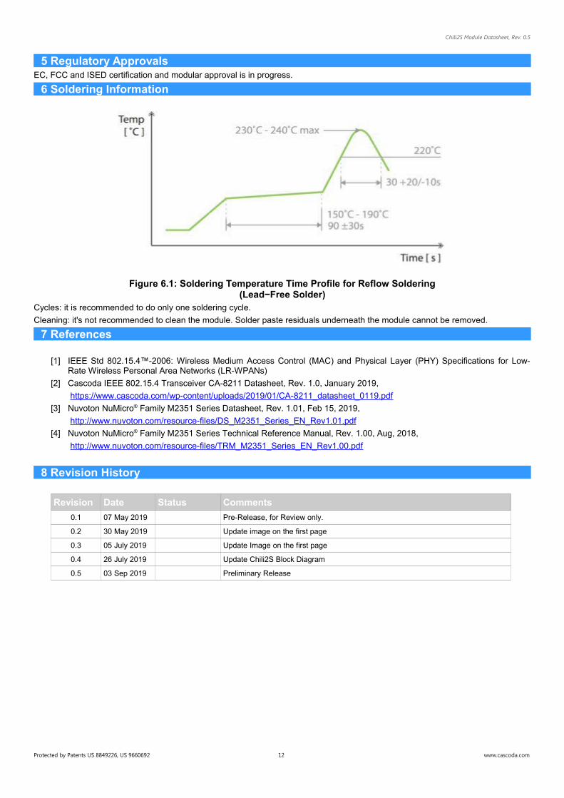
6 Soldering Information
Figure 6.1: Soldering Temperature Time Profile for Reflow Soldering(Lead−Free Solder)
Cycles: it is recommended to do only one soldering cycle.
Cleaning: it's not recommended to clean the module. Solder paste residuals underneath the module cannot be removed.
7 References
[1] IEEE Std 802.15.4™-2006: Wireless Medium Access Control (MAC) and Physical Layer (PHY) Specifications for Low-Rate Wireless Personal Area Networks (LR-WPANs)
[2] Cascoda IEEE 802.15.4 Transceiver CA-8211 Datasheet, Rev. 1.0, January 2019,
https://www.cascoda.com/wp-content/uploads/2019/01/CA-8211_datasheet_0119.pdf
[3] Nuvoton NuMicro® Family M2351 Series Datasheet, Rev. 1.01, Feb 15, 2019,
http://www.nuvoton.com/resource-files/DS_M2351_Series_EN_Rev1.01.pdf
[4] Nuvoton NuMicro® Family M2351 Series Technical Reference Manual, Rev. 1.00, Aug, 2018,
http://www.nuvoton.com/resource-files/TRM_M2351_Series_EN_Rev1.00.pdf
8 Revision History
Revision Date Status Comments
0.1 07 May 2019 Pre-Release, for Review only.
0.2 30 May 2019 Update image on the first page
0.3 05 July 2019 Update Image on the first page
0.4 26 July 2019 Update Chili2S Block Diagram
0.5 03 Sep 2019 Preliminary Release
Protected by Patents US 8849226, US 9660692 12 www.cascoda.com