Embed Size (px)
Citation preview

REV. 1.1 DW01A-DS-11_EN JUN 2010
Datasheet
DW01A One Cell Lithium-ion/Polymer Battery Protection IC
FORTU
NE’
Prope
rties
For R
efere
nce O
nly

DW01A
Rev. 1.1 2/14
Fortune Semiconductor Corporation
富晶電子股份有限公司
28F., No.27, Sec. 2, Zhongzheng E. Rd., Danshui Town, Taipei County 251, Taiwan Tel.:886-2-28094742 Fax:886-2-28094874 www.ic-fortune.com
This manual contains new product information. Fortune Semiconductor Corporation reserves the rights to modify the product specification without further notice. No liability is assumed by Fortune Semiconductor
Corporation as a result of the use of this product. No rights under any patent accompany the sale of the product.
FORTU
NE’
Prope
rties
For R
efere
nce O
nly
DW01A
Rev. 1.1 3/14
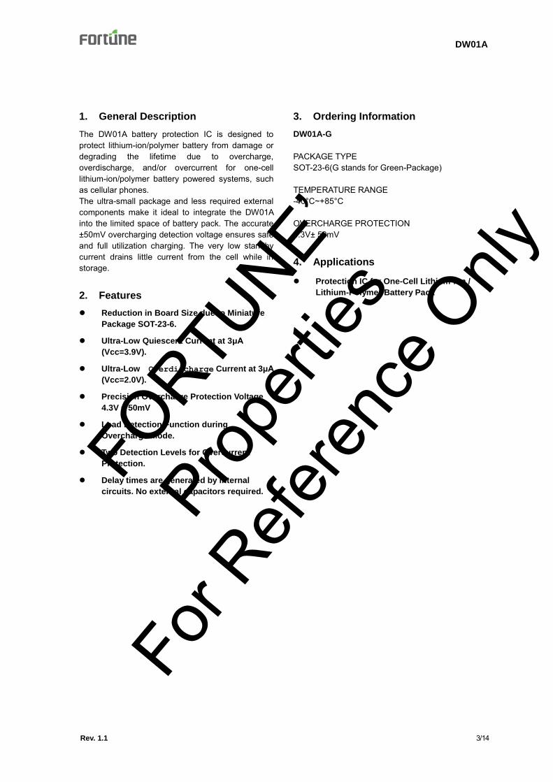
1. General Description
The DW01A battery protection IC is designed to protect lithium-ion/polymer battery from damage or degrading the lifetime due to overcharge, overdischarge, and/or overcurrent for one-cell lithium-ion/polymer battery powered systems, such as cellular phones. The ultra-small package and less required external components make it ideal to integrate the DW01A into the limited space of battery pack. The accurate ±50mV overcharging detection voltage ensures safe and full utilization charging. The very low standby current drains little current from the cell while in storage.
2. Features
Reduction in Board Size due to Miniature
Package SOT-23-6.
Ultra-Low Quiescent Current at 3μA
(Vcc=3.9V).
Ultra-Low Overdischarge Current at 3μA
(Vcc=2.0V).
Precision Overcharge Protection Voltage
4.3V ± 50mV
Load Detection Function during
Overcharge Mode.
Two Detection Levels for Overcurrent
Protection.
Delay times are generated by internal
circuits. No external capacitors required.
3. Ordering Information
DW01A-G
PACKAGE TYPE SOT-23-6(G stands for Green-Package) TEMPERATURE RANGE -40°C~+85°C OVERCHARGE PROTECTION 4.3V± 50mV
4. Applications
Protection IC for One-Cell Lithium-Ion /
Lithium-Polymer Battery Pack
FORTU
NE’
Prope
rties
For R
efere
nce O
nly

DW01A
Rev. 1.1 4/14
5. Product Name List
Model Package
Overcharge
detection
voltage
[VOCP] (V)
Overcharge
release
voltage
[VOCR] (V)
Overdischarge
detection
voltage
[VODP] (V)
Overdischarge
release
voltage
[VODR] (V)
Overcurrent
detection
voltage
[VOI1] (mV)
DW01A SOT-23-6 4.3000.050 4.1000.050 2.400.100 3.00.100 15030
6. Pin Configuration and Package Marking Information
Pin No. Symbol Description
1 OD MOSFET gate connection pin for discharge control
2 CS Input pin for current sense, charger detect
3 OC MOSFET gate connection pin for charge control
4 TD Test pin for reduce delay time
5 VCC Power supply, through a resistor (R1)
6 GND Ground pin
DW01 W...
.... A
Top Point and Under_line:Lot No. Bottom Point:Year w : week, A~Z & A ~ Z
5
1 2 3
6 4
DW01A
FORTU
NE’
Prope
rties
For R
efere
nce O
nly
DW01A
Rev. 1.1 5/14
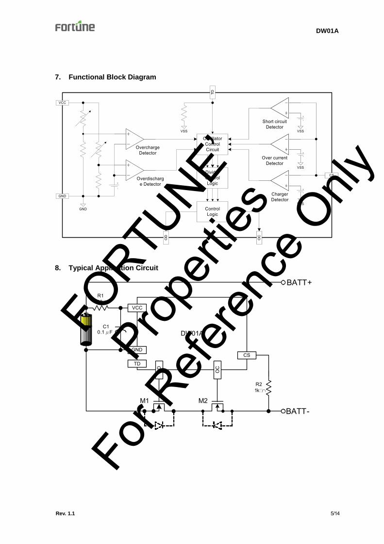
7. Functional Block Diagram
GND
OC
VSS
VSS
VSS
VCC
GND
CS
ChargerDetector
OD
ControlLogic
Short circuitDetector
Over currentDetector
OscillatorControlCircuitOvercharge
Detector
Overdischarge Detector
DividerControlLogic
TD
VSS
8. Typical Application Circuit
DW01A
OC
OD
GNDCS
BATT-M1 M2
R21k
R1100
VCC
BATT+
TD
C10.1μF
FORTU
NE’
Prope
rties
For R
efere
nce O
nly
DW01A
Rev. 1.1 6/14
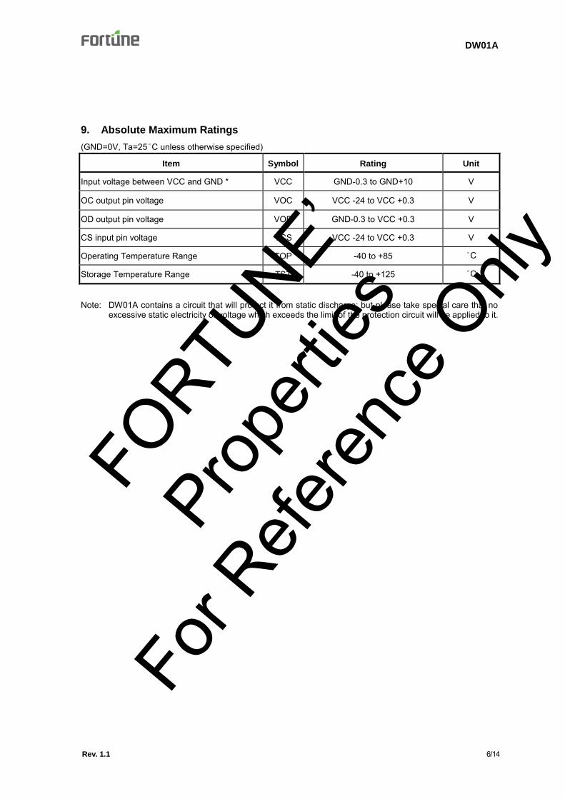
9. Absolute Maximum Ratings
(GND=0V, Ta=25°C unless otherwise specified)
Item Symbol Rating Unit
Input voltage between VCC and GND * VCC GND-0.3 to GND+10 V
OC output pin voltage VOC VCC -24 to VCC +0.3 V
OD output pin voltage VOD GND-0.3 to VCC +0.3 V
CS input pin voltage VCS VCC -24 to VCC +0.3 V
Operating Temperature Range TOP -40 to +85 °C
Storage Temperature Range TST -40 to +125 °C
Note: DW01A contains a circuit that will protect it from static discharge; but please take special care that no excessive static electricity or voltage which exceeds the limit of the protection circuit will be applied to it.
FORTU
NE’
Prope
rties
For R
efere
nce O
nly

DW01A
Rev. 1.1 7/14
10. Electrical Characteristics
(Ta=25°C unless otherwise specified)
PARAMETER TEST CONDITIONS SYMBOL Min Typ Max UNIT
Supply Current VCC=3.9V ICC 3.0 6.0 μA
Overdischarge Current VCC=2.0V IOD 1.5 3 μA
Overcharge Protection Voltage DW01A VOCP 4.25 4.30 4.35 V
Overcharge Release Voltage VOCR 4.05 4.10 4.15 V
Overdischarge Protection Voltage VODP 2.30 2.40 2.50 V
Overdischarge Release Voltage VODR 2.90 3.00 3.10 V
Overcurrent Protection Voltage VOIP(VOI1) 120 150 180 mV
Short Current Protection Voltage VCC=3.6V VSIP(VOI2) 1.00 1.35 1.70 V
Overcharge Delay Time TOC 80 200 ms
Overdischarge Delay Time VCC=3.6V to 2.0V TOD 40 100 ms
Overcurrent Delay Time (1) VCC=3.6V TOI1 10 20 ms
Overcurrent Delay Time (2) VCC=3.6V TOI2 5 50 μs
Charger Detection Threshold Voltage
VCHA -1.2 -0.7 -0.2 V
OD Pin Output “H” Voltage VDH VCC-0.1 VCC-0.02 V
OD Pin Output “L” Voltage VDL 0. 1 0.5 V
OC Pin Output “H” Voltage VCH VCC-0.1 VCC-0.02 V
OC Pin Output “L” Voltage VCL 0.1 0.5 V
FORTU
NE’
Prope
rties
For R
efere
nce O
nly

DW01A
Rev. 1.1 8/14
11. Description of Operation
Normal Condition
If VODP<VCC<VOCP and VCH<VCS<VOI1, M1 and M2 are both turned on. The charging and discharging processes can be operated normally.
Overcharge Protection
When the voltage of the battery cell exceeds the overcharge protection voltage (VOCP) beyond the overcharge delay time (TOC) period, charging is inhibited by turning off of the charge control MOSFET. The overcharge condition is released in two cases: The voltage of the battery cell becomes lower than the overcharge release voltage (VOCR) through self-discharge. The voltage of the battery cell falls below the overcharge protection voltage (VOCP) and a load is connected. When the battery voltage is above VOCP, the overcharge condition will not release even a load is connected to the pack.
Overdischarge Protection
When the voltage of the battery cell goes below the overdischarge protection voltage (VODP) beyond the overdischarge delay time (TOD) period, discharging is inhibited by turning off the discharge control MOSFET. The default of overdischarge delay time is 10ms. Inhibition of discharging is immediately released when the voltage of the battery cell becomes higher than overdischarge release voltage (VODR) through charging.
Overcurrent Protection
In normal mode, the DW01A continuously monitors the discharge current by sensing the voltage of CS pin. If the voltage of CS pin exceeds the overcurrent protection voltage (VOIP) beyond the overcurrent delay time (TOI1) period, the overcurrent protection circuit operates and discharging is inhibited by turning off the discharge control MOSFET. The overcurrent condition returns to the normal mode when the load is released or the impedance between BATT+ and BATT- is larger than 500kΩ. The DW01A provides two overcurrent detection levels (0.15V and 1.35V) with two overcurrent delay time (TOI1 and TOI2) corresponding to each overcurrent detection level.
Charge Detection after Overdischarge
When overdischarge occurs, the discharge control MOSFET turns off and discharging is inhibited. However, charging is still permitted through the parasitic diode of MOSFET. Once the charger is connected to the battery pack, the DW01A immediately turns on all the timing generation and detection circuitry. Charging progress is sensed if the voltage between CS and GND is below charge detection threshold voltage (VCH).
Auto Power Down recovery
The IC continues to operate even after the overdischarge state has been entered. The battery voltage rising to the overdischarge release voltage(VODR) or higher is the only required condition for the IC to return to the normal state.
FORTU
NE’
Prope
rties
For R
efere
nce O
nly

DW01A
Rev. 1.1 9/14
12. Design Guide
Selection of External Control MOSFET
Because the overcurrent protection voltage is preset, the threshold current for overcurrent detection is determined by the turn-on resistance of the charge and discharge control MOSFETs. The turn-on resistance of the external control MOSFETs can be determined by the equation: RON=VOIP/ (2 x IT) (IT is the overcurrent threshold current). For example, if the overcurrent threshold current IT is designed to be 3A, the turn-on resistance of the external control MOSFET must be 25mΩ. Be aware that turn-on resistance of the MOSFET changes with temperature variation due to heat dissipation. It changes with the voltage between gate and source as well. (Turn-on resistance of MOSFET increases as the voltage between gate and source decreases).
As the turn-on resistance of the external MOSFET changes, the design of the overcurrent threshold current changes accordingly.
Suppressing the Ripple and Disturbance from Charger
To suppress the ripple and disturbance from charger, connecting R1 and C1 to VCC is recommended.
Protection the CS pin
R2 is used for latch-up protection when charger is connected under overdischarge condition and overstress protection at reverse connecting of a charger.
FORTU
NE’
Prope
rties
For R
efere
nce O
nly

DW01A
Rev. 1.1 10/14
13. Timing Diagram
Overcharge Condition Load Discharging Normal Condition
VOCP
VOCR
VODR
VODP
Charger
Load
VCC
CS
VCC
GND
VCC
GND
Bat
tery
Vol
tage
OC
Pin
OD
Pin
CS
Pin
TOC TOC
VOI1
VCH
FORTU
NE’
Prope
rties
For R
efere
nce O
nly

DW01A
Rev. 1.1 11/14
Overdischarge Condition Charging by a Charger Normal Condition
VOCP
VOCR
VODR
VODP
Charger
Load
VCC
CS
VCC
GND
VCC
GND
Bat
tery
Vol
tage
OC
Pin
OD
Pin
CS
Pin
TOD TOD
VCH
VOI2
FORTU
NE’
Prope
rties
For R
efere
nce O
nly

DW01A
Rev. 1.1 12/14
Over Current Condition Normal Condition
VOCP
VOCR
VODR
VODP
Charger
Load
VCC
CS
VCC
GND
VCC
VOI1
Bat
tery
Vol
tage
OC
Pin
OD
Pin
CS
Pin
TOI1TOI2
GND
VOI2
FORTU
NE’
Prope
rties
For R
efere
nce O
nly

DW01A
Rev. 1.1 13/14
14. Package Outline
Dimension (Package A)
e
e1
b
E
D
E1
1
2
A2A
A1 L
L1
GAUGE PLANE
SEATING PLANE
DETAIL A
c
DETAIL ASYMBOL MIN. TYP. MAX.
AA1A2b
cDE
E1
ee1
LL1
1 3
0 55
107
1.05 - 1.350.05 - 0.151.00 1.10 1.200.40 - 0.55
0.08 - 0.20
0.35 0.45 0.55
0.95 BSC.1.90 BSC.
0.60 REF.
Unit : mm
b2
b2 0.25 - 0.40
2.70 2.90 3.002.60 2.80 3.001.50 1.60 1.70
2 6 8 10
Dimension (Package B)
e
e1
b
E1
D
E
A2A
A1 L1
L
GAUGE PLANE
SEATING PLANE
DETAIL A
c
DETAIL ASYMBOL MIN. TYP. MAX.
AA1A2bcDEE1
LL1
ee1
0 - 8
1.050 - 1.2500.000 - 0.1001.050 - 1.1500.300 - 0.4000.100 - 0.200
1.800 - 2.0000.700REF
0.950 TYP
Unit : mm
2.820 - 3.0201.500 - 1.7002.650 - 2.950
0.300 - 0.600
0.2
FORTU
NE’
Prope
rties
For R
efere
nce O
nly

DW01A
Rev. 1.1 14/14
15. Revision History
Version Date Page Description
1.0 2009/06/24 ALL New release 1.1 2010/06/10 8 Add Auto Power Down recovery
FORTU
NE’
Prope
rties
For R
efere
nce O
nly