Embed Size (px)
Citation preview
Materials Science and Engineering B87 (2001) 1–22
Review
Real-time optical characterization of thin film growth
N. Dietz *Department of Physics and Astronomy, Georgia State Uni�ersity, Atlanta, GA 30303, USA
Accepted 21 June 2001
Abstract
The further spatial reduction together with stringent thickness and composition tolerances in manufacturing of advancedelectronic and optical devices require new approaches to control the growth process as well as to improve the insight into thedeposition process itself. The development of non-invasive, real-time, structure-specific analytical tools for characterizingphenomena occurring at surfaces and interfaces during thin film growth has therefore to address both, providing a detailedunderstanding of the thin film growth process and providing robust process control signals in real-time. This review gives anoverview of the principles of angle resolved reflectance techniques applied to real-time thin film process monitoring, the study ofsurface reaction kinetics, and to growth process control. The capabilities of high-sensitive thin film growth monitoring and controlare illustrated for the growth of III-V compounds under pulsed chemical beam epitaxy conditions, using p-polarized reflectancespectroscopy as an example. © 2001 Published by Elsevier Science B.V.
Keywords: Optical characterization; Thin film growth; Chemical beam epitaxy
www.elsevier.com/locate/mseb
1. Introduction
The development of surface-sensitive real-time opti-cal characterization techniques that are able to giveinsights in the surface reaction kinetics during deposi-tion or etching processes are essential for further pro-gress in understanding and controlling such processes.For example, the defect formation and the interactions/propagation during heteroepitaxial growth requires theunderstanding and control of the kinetics of heteroepi-taxy, which is closely related to surface structure thatdepends on both reconstruction and the nature anddistribution of defects in the epitaxial film. Eventhough, reduced pressure deposition methods such asorganometallic chemical vapor deposition (OMCVD),chemical beam epitaxy (CBE), or plasma enhancedchemical vapor deposition play an important role inmanufacturing, the progress in understanding and con-trolling these processes has been very slow, consideringhow limited our knowledge is about chemical reaction
pathways, the reaction kinetics during the decomposi-tion process of organometallic precursors, or the corre-lation to defect formation in the growth of compoundsemiconductors. In addition, the stringent tolerances inthe engineering of advanced optoelectronic integratedcircuits with respect to control thickness and composi-tion of ultra-thin layers require the development ofmonitoring and control techniques that follow the de-position process with sub-monolayer resolution [1].
Optical characterization techniques are becoming im-portant tools for in-situ or real-time monitoring inmaterials research with advances particularly in theareas of non-intrusive thin film characterization andprocess control. However, optical probes have severalwell-know limitations regarding the spectral wavelengthrange accessible, sensitivity towards surface processes,or their complexity in implementation and/or interpre-tation. Most reflectance-based techniques such as dy-namic optical reflectivity (DOS) [2–4], spectral resolvednormal incidence reflectance spectroscopy (NRIS) [5,6]or pyrometric interferometry (PI) [7] are successfullyapplied to various deposition processes and provideinformation on both the growth rate and the composi-
* Tel.: +1-404-463-9617; fax: +1-404-651-3419.E-mail address: [email protected] (N. Dietz).
0921-5107/01/$ - see front matter © 2001 Published by Elsevier Science B.V.PII: S0 9 21 -5107 (01 )00711 -5
N. Dietz / Materials Science and Engineering B87 (2001) 1–222
tion of the deposits, however, they are relatively insensi-tive to surface processes that drive deposition or etch-ing processes.
The sensitivity of optical probe techniques is deter-mined approximately by the ratio of the penetrationdepth of light to the thickness of the surface layer,which is for CBE/OMCVD processes in the order of100:1. Thus the reflected beam carries roughly 99%bulk and only 1% surface relevant information. Takinginto account light source instabilities (typically �1%)and detector limitation (noise and dynamic range),signal contributions smaller than 1% are hardly toresolve by standard reflectance/transmission techniques.
The urge to gain a better understanding to surfaceprocesses led to the development of surface-sensitivereal-time optical sensor techniques [8] such as reflec-tance-difference spectroscopy (RDS) [1,9–11], surfacephoto absorption (SPA) [12–14], p-polarized reflec-tance spectroscopy (PRS) [15–17] and laser light scat-tering (LLS) [18], which are providing new insights intosurface chemistry and surface reconstruction and sur-face morphology during growth. Those techniques areable to characterize and monitor surface processes inthe vicinity where the growth occurs, which, for exam-ple, in a CBE process is the surface reaction layer(SRL), built up of physisorbed and chemisorbed pre-cursor fragments between the ambient and filminterface.
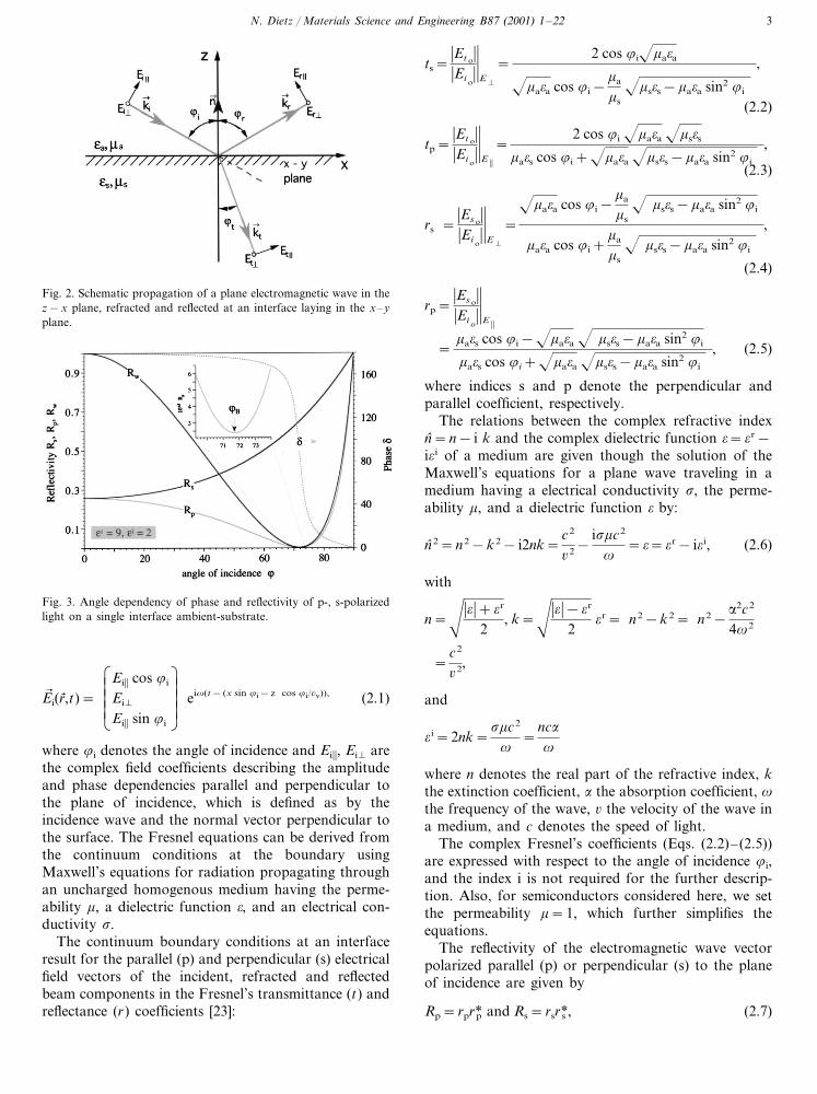
However, applying optical probe techniques towardsreal-time characterization of thin film growth also in-herits the challenge to relate surface chemistry processesthat drives the growth process, towards growth/filmproperties, such as composition, instantaneous growthrate or structural layer quality. As illustrated in Fig. 1,
in deposition four primary regions are involved.Presently, most characterization techniques are beingdirected towards accurately measuring ambient processparameters, such as pressure, flux or temperature, sincenumerous probes are available to provide a relativedetailed assessment of the ambient. This strategy isclearly limited in its capability to deal with complexnonlinear surface chemistry processes, where the sur-face plays an integral role in the precursor decomposi-tion pathways and small changes in the ambientcomposition can affect the growth substantially.
The development of diagnostic tools that are basedon interaction of light with mater gaining increasinglyof importance for industrial applications in communi-cations, process control, environmental pollution moni-toring and medical diagnostics. These type of devicesare based in one way or the other on the analysis of thelight before and after the interaction with matter inorder to gain information about the matter itself—or— to changes at the interfaces of ambient or matters.Also, the use of optical sensors for the real-time moni-toring of etching and/or growth processes is favoredbecause of their non-destructive character and some ofthese methods are ideal to monitor the overall growthprocess and/or substrate temperature in industrial ap-plications, requiring low cost and maintenance.
The following chapters briefly summarize the physi-cal principles on which reflectance methods are based.The review is focusing on angle resolved reflectancetechniques and in particular pseudo-Brewster anglereflectance configuration techniques applied to thin filmprocess characterization or the study of surface reactionkinetics. In the last section, the use of PRS for thin filmgrowth monitoring and control will be discussed.
2. Reflectance methods
The electromagnetic radiation interacting with mattercan be described either as an electromagnetic wave thatis defined by electric and magnetic field oscillating withthe frequency �, or as a photon (quantized particle)with an energy ��. For the detection diagnostics de-scribed here, the wave picture of light is sufficient forthe description of the interaction process and only thematter will be treated quantum mechanically. Compre-hensive descriptions of optics and applications of opticscan be found in the works by Born and wolf [19],Azzam and Bashara [20], Herman [21] and Bauer [22].The notation used here complies with the ‘Nebraskaoptical conventions’ [20] and all expressions are givenin MKSA (SI) units.
An incidence plane wave front traveling in the x–z-plane in kb 1-direction with the velocity �1 (see Fig. 2), inan orthogonal coordinate system can be represented as
Fig. 1. The four primary regions involved in deposition are: (1) theambient; (2) the surface reaction layer, which consists of speciesphysisorbed or chemisorbed to the surface in dynamic equilibriumwith both ambient and surface; (3) the surface itself; and (4) thenear-surface region that can be defined as consisting of the outermostseveral atomic layers of the fabricated sample.
N. Dietz / Materials Science and Engineering B87 (2001) 1–22 3
Fig. 2. Schematic propagation of a plane electromagnetic wave in thez−x plane, refracted and reflected at an interface laying in the x–yplane.
ts=�Et o
��Ei o
��E �
=2 cos �i��a�a
��a�a cos �i−�a
�s
��s�s−�a�a sin2 �i
,
(2.2)
tp=�Et o
��Ei o
��E ��
=2 cos �i ��a�a ��s�s
�a�s cos �i+��a�a ��s�s−�a�a sin2 �i
,
(2.3)
rs =�Es o
��Ei o
��E �
=��a�a cos �i−
�a
�s
� �s�s−�a�a sin2 �i
�a�a cos �i+�a
�s
� �s�s−�a�a sin2 �i
,
(2.4)
rp=�Es o
��Ei o
��E ��
=�a�s cos �i−��a�a � �s�s−�a�a sin2 �i
�a�s cos �i+��a�a ��s�s−�a�a sin2 �i
, (2.5)
where indices s and p denote the perpendicular andparallel coefficient, respectively.
The relations between the complex refractive indexn=n− i k and the complex dielectric function �=� r−i� i of a medium are given though the solution of theMaxwell’s equations for a plane wave traveling in amedium having a electrical conductivity �, the perme-ability �, and a dielectric function � by:
n2=n2−k2− i2nk=c2
�2−i��c2
�=�=� r− i� i, (2.6)
with
n=��� �+� r
2, k=
��� �−� r
2� r= n2−k2= n2−
�2c2
4�2
=c2
�2,
and
� i=2nk=��c2
�=
nc�
�
where n denotes the real part of the refractive index, kthe extinction coefficient, � the absorption coefficient, �
the frequency of the wave, � the velocity of the wave ina medium, and c denotes the speed of light.
The complex Fresnel’s coefficients (Eqs. (2.2)– (2.5))are expressed with respect to the angle of incidence �i,and the index i is not required for the further descrip-tion. Also, for semiconductors considered here, we setthe permeability �=1, which further simplifies theequations.
The reflectivity of the electromagnetic wave vectorpolarized parallel (p) or perpendicular (s) to the planeof incidence are given by
Rp=rprp* and Rs=rsr s*, (2.7)
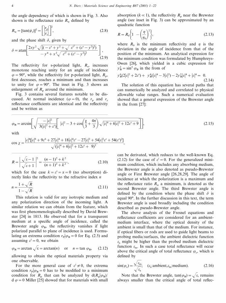
Fig. 3. Angle dependency of phase and reflectivity of p-, s-polarizedlight on a single interface ambient-substrate.
Eb i(r� ,t)=
�����
Ei�� cos �i
Ei�
Ei�� sin �i
�����
ei�(t− (x sin �i−z cos �i/�v)), (2.1)
where �i denotes the angle of incidence and Ei��, Ei� arethe complex field coefficients describing the amplitudeand phase dependencies parallel and perpendicular tothe plane of incidence, which is defined as by theincidence wave and the normal vector perpendicular tothe surface. The Fresnel equations can be derived fromthe continuum conditions at the boundary usingMaxwell’s equations for radiation propagating throughan uncharged homogenous medium having the perme-ability �, a dielectric function �, and an electrical con-ductivity �.
The continuum boundary conditions at an interfaceresult for the parallel (p) and perpendicular (s) electricalfield vectors of the incident, refracted and reflectedbeam components in the Fresnel’s transmittance (t) andreflectance (r) coefficients [23]:
N. Dietz / Materials Science and Engineering B87 (2001) 1–224
the angle dependency of which is shown in Fig. 3. Alsoshown is the reflectance ratio Rw defined by
Rw= [tan(�r)]2=��rp�
�rs�n2
, (2.8)
and the phase shift , given by
=atan�2xy2 �1
2(−� r+y2+� � i2+ (� r−y2)2)
−y4+x2� � i2+ (� r−y2)2
n,
(2.9)
The reflectivity for s-polarized light, Rs, increasesmonotone reaching unity for an angle of incidence�=90°, while the reflectivity for p-polarized light, Rp,first decreases, reaches a minimum and than increasesto unity for �=90°. The inset in Fig. 3 shows anenlargement of Rp around the minimum.
Fig. 3 contains several features notable to be dis-cussed. At normal incidence (�=0), the rp and rs
reflectance coefficients are identical and the reflectivityand be written as
R=� ��−1
��+1
�2=
(n−1)2+k2
(n+1)2+k2 , (2.10)
which for the case k=� i=�=0 (no absorption) di-rectly links the reflectivity to the refractive index n
n=1+�R
1−�R. (2.11)
This relation is valid for any isotropic medium andany polarization direction of the incoming light. Asimilar relation we can obtain from the feature, whichwas first phenomenologically described by David Brew-ster [24] in 1813. He observed that for a transparentmedium at a specific angle of incidence, called theBrewster angle �B, the reflectivity vanishes if lightpolarized parallel to plane of incidence is used. Formu-lating an extrema condition rP��B=0 for Eq. (2.5) andassuming � i=0, we obtain
�B=arctan ��=arctan(n) or n= tan �B, (2.12)
allowing to obtain the optical materials property viaone observable.
For the more general case of � i�0, the extremacondition rP��B=0 has to be modified to a minimumcondition for Rp that can be analyzed by d(Rp��B)/d �=0 Miller [25] showed that for materials with small
absorption (k�1), the reflectivity Rp near the Brewsterangle (see inset in Fig. 3) can be approximated by anquadratic function
R=R0�
1 −�
0
�2, (2.13)
where R0 is the minimum reflectivity and is thedeviation in the angle of incidence from that of theposition of the minimum. An analytical expression forthe minimum condition was formulated by Humphreys-Owen [26], which yielded in a cubic expression foryB
2 =sin2 �B in the from of
yB6 (2�� �2+2� r)+ yB
4 (�� �4−3�� �2)−2yB2 �� �4+ �� �4= 0.
(2.14)The solution of this equation has several paths that
can numerically be analyzed and correlated to physicalallowable value ranges. Such a numerical evaluationshowed that a general expression of the Brewster anglein the from [27]:
can be derivated, which reduces to the well-known Eq.(2.12) for the case of � i=0. For the generalized mini-mum condition, which includes any absorbing medium,the Brewster angle is also denoted as pseudo-Brewsterangle or First Brewster angle [26,28,29]. The angle ofincidence at which the polarization is a maximum andthe reflectance ratio Rw a minimum, is denoted as thesecond Brewster angle. The third Brewster angle isdefined by the condition where the phase shift isequal 90°. In the further discussion in this text, the termBrewster angle is used broadly including the conditiondescribed as pseudo-Brewster angle.
The above analysis of the Fresnel equations andreflectance coefficients are considered for an ambient-medium interface, where the optical density of theambient is small than that of the medium. For instance,if optical fibers or rods are used to guide light beams toprobing media/surfaces, the ambient dielectric function�a might be higher than the probed medium dielectricfunction �m. In such a case total reflectance will occurabove the critical angle of total reflectance �c, which isdefined by
sin(�c)=��m
��a
; (�a:ambient,�m:medium). (2.16)
Note that the Brewster angle, tan(�B)=��, remainsalways smaller than the critical angle of total reflec-
�B=arcsin�� − �� �2
3(�� �2+� r)� �� �2−3+cos
��3+
4�3� ��� �4+6�� �2+12� r+9
nn, (2.15)
with
cos �=�� �4[�� �8+9�6+27�� �4+18�� �4� r−27�� �2+54�� �2� r+54(� r)2]
�(�� �4+6�� �2+12� r+ 9)3,
N. Dietz / Materials Science and Engineering B87 (2001) 1–22 5
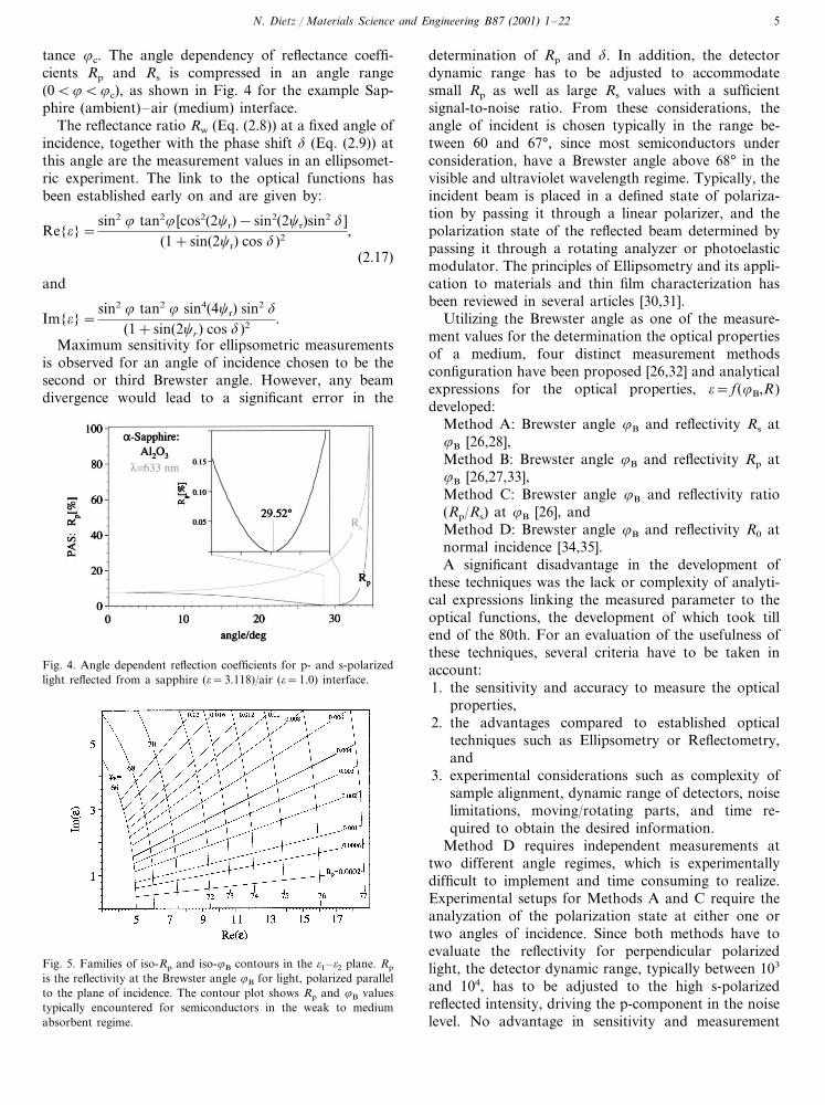
tance �c. The angle dependency of reflectance coeffi-cients Rp and Rs is compressed in an angle range(0����c), as shown in Fig. 4 for the example Sap-phire (ambient)–air (medium) interface.
The reflectance ratio Rw (Eq. (2.8)) at a fixed angle ofincidence, together with the phase shift (Eq. (2.9)) atthis angle are the measurement values in an ellipsomet-ric experiment. The link to the optical functions hasbeen established early on and are given by:
Re{�}=sin2 � tan2� [cos2(2�r)−sin2(2�r)sin2 ]
(1+sin(2�r) cos )2 ,
(2.17)
and
Im{�}=sin2 � tan2 � sin4(4�r) sin2
(1+sin(2�r) cos )2 .
Maximum sensitivity for ellipsometric measurementsis observed for an angle of incidence chosen to be thesecond or third Brewster angle. However, any beamdivergence would lead to a significant error in the
determination of Rp and . In addition, the detectordynamic range has to be adjusted to accommodatesmall Rp as well as large Rs values with a sufficientsignal-to-noise ratio. From these considerations, theangle of incident is chosen typically in the range be-tween 60 and 67°, since most semiconductors underconsideration, have a Brewster angle above 68° in thevisible and ultraviolet wavelength regime. Typically, theincident beam is placed in a defined state of polariza-tion by passing it through a linear polarizer, and thepolarization state of the reflected beam determined bypassing it through a rotating analyzer or photoelasticmodulator. The principles of Ellipsometry and its appli-cation to materials and thin film characterization hasbeen reviewed in several articles [30,31].
Utilizing the Brewster angle as one of the measure-ment values for the determination the optical propertiesof a medium, four distinct measurement methodsconfiguration have been proposed [26,32] and analyticalexpressions for the optical properties, �= f(�B,R)developed:
Method A: Brewster angle �B and reflectivity Rs at�B [26,28],Method B: Brewster angle �B and reflectivity Rp at�B [26,27,33],Method C: Brewster angle �B and reflectivity ratio(Rp/Rs) at �B [26], andMethod D: Brewster angle �B and reflectivity R0 atnormal incidence [34,35].A significant disadvantage in the development of
these techniques was the lack or complexity of analyti-cal expressions linking the measured parameter to theoptical functions, the development of which took tillend of the 80th. For an evaluation of the usefulness ofthese techniques, several criteria have to be taken inaccount:1. the sensitivity and accuracy to measure the optical
properties,2. the advantages compared to established optical
techniques such as Ellipsometry or Reflectometry,and
3. experimental considerations such as complexity ofsample alignment, dynamic range of detectors, noiselimitations, moving/rotating parts, and time re-quired to obtain the desired information.
Method D requires independent measurements attwo different angle regimes, which is experimentallydifficult to implement and time consuming to realize.Experimental setups for Methods A and C require theanalyzation of the polarization state at either one ortwo angles of incidence. Since both methods have toevaluate the reflectivity for perpendicular polarizedlight, the detector dynamic range, typically between 103
and 104, has to be adjusted to the high s-polarizedreflected intensity, driving the p-component in the noiselevel. No advantage in sensitivity and measurement
Fig. 4. Angle dependent reflection coefficients for p- and s-polarizedlight reflected from a sapphire (�=3.118)/air (�=1.0) interface.
Fig. 5. Families of iso-Rp and iso-�B contours in the �1–�2 plane. Rp
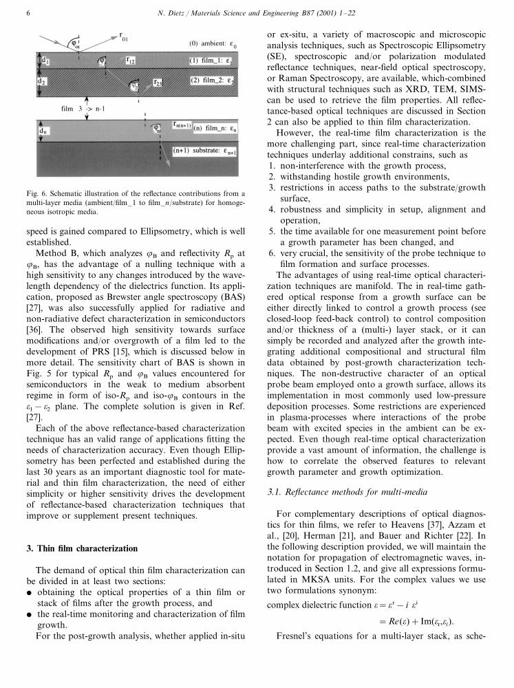
is the reflectivity at the Brewster angle �B for light, polarized parallelto the plane of incidence. The contour plot shows Rp and �B valuestypically encountered for semiconductors in the weak to mediumabsorbent regime.
N. Dietz / Materials Science and Engineering B87 (2001) 1–226
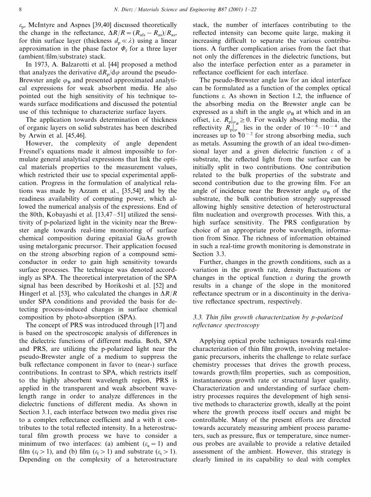
Fig. 6. Schematic illustration of the reflectance contributions from amulti-layer media (ambient/film–1 to film–n/substrate) for homoge-neous isotropic media.
or ex-situ, a variety of macroscopic and microscopicanalysis techniques, such as Spectroscopic Ellipsometry(SE), spectroscopic and/or polarization modulatedreflectance techniques, near-field optical spectroscopy,or Raman Spectroscopy, are available, which-combinedwith structural techniques such as XRD, TEM, SIMS-can be used to retrieve the film properties. All reflec-tance-based optical techniques are discussed in Section2 can also be applied to thin film characterization.
However, the real-time film characterization is themore challenging part, since real-time characterizationtechniques underlay additional constrains, such as1. non-interference with the growth process,2. withstanding hostile growth environments,3. restrictions in access paths to the substrate/growth
surface,4. robustness and simplicity in setup, alignment and
operation,5. the time available for one measurement point before
a growth parameter has been changed, and6. very crucial, the sensitivity of the probe technique to
film formation and surface processes.The advantages of using real-time optical characteri-
zation techniques are manifold. The in real-time gath-ered optical response from a growth surface can beeither directly linked to control a growth process (seeclosed-loop feed-back control) to control compositionand/or thickness of a (multi-) layer stack, or it cansimply be recorded and analyzed after the growth inte-grating additional compositional and structural filmdata obtained by post-growth characterization tech-niques. The non-destructive character of an opticalprobe beam employed onto a growth surface, allows itsimplementation in most commonly used low-pressuredeposition processes. Some restrictions are experiencedin plasma-processes where interactions of the probebeam with excited species in the ambient can be ex-pected. Even though real-time optical characterizationprovide a vast amount of information, the challenge ishow to correlate the observed features to relevantgrowth parameter and growth optimization.
3.1. Reflectance methods for multi-media
For complementary descriptions of optical diagnos-tics for thin films, we refer to Heavens [37], Azzam etal., [20], Herman [21], and Bauer and Richter [22]. Inthe following description provided, we will maintain thenotation for propagation of electromagnetic waves, in-troduced in Section 1.2, and give all expressions formu-lated in MKSA units. For the complex values we usetwo formulations synonym:
complex dielectric function �=� r− i � i
=Re(�)+Im(�r,�i).
Fresnel’s equations for a multi-layer stack, as sche-
speed is gained compared to Ellipsometry, which is wellestablished.
Method B, which analyzes �B and reflectivity Rp at�B, has the advantage of a nulling technique with ahigh sensitivity to any changes introduced by the wave-length dependency of the dielectrics function. Its appli-cation, proposed as Brewster angle spectroscopy (BAS)[27], was also successfully applied for radiative andnon-radiative defect characterization in semiconductors[36]. The observed high sensitivity towards surfacemodifications and/or overgrowth of a film led to thedevelopment of PRS [15], which is discussed below inmore detail. The sensitivity chart of BAS is shown inFig. 5 for typical Rp and �B values encountered forsemiconductors in the weak to medium absorbentregime in form of iso-Rp and iso-�B contours in the�1−�2 plane. The complete solution is given in Ref.[27].
Each of the above reflectance-based characterizationtechnique has an valid range of applications fitting theneeds of characterization accuracy. Even though Ellip-sometry has been perfected and established during thelast 30 years as an important diagnostic tool for mate-rial and thin film characterization, the need of eithersimplicity or higher sensitivity drives the developmentof reflectance-based characterization techniques thatimprove or supplement present techniques.
3. Thin film characterization
The demand of optical thin film characterization canbe divided in at least two sections:� obtaining the optical properties of a thin film or
stack of films after the growth process, and� the real-time monitoring and characterization of film
growth.For the post-growth analysis, whether applied in-situ
N. Dietz / Materials Science and Engineering B87 (2001) 1–22 7
matically shown in Fig. 6, are used to calculate thechanges of the reflectivity for s- or p-polarized light asa function of layer thickness, assuming homogenousisotropic media. Numbering the media forming themulti-layer stack through, starting with ‘0’ for ambient,the reflectance coefficients rk(k+1) for the interfaces aregiven in Ref. [37]
rp�k(k+1)=�k+1 ��k−�0 sin2 �−�k ��k+1−�0 sin2 �
�k+1 ��k−�0 sin2 �+�k ��k+1−�0 sin2 �
(k�0). (3.1)
and
rs�k(k+1)=��kcos �−��k+1−�0 sin2 �
��kcos �+��k+1−�0 sin2 �(k�0).
(3.2)
To determine the total reflected beam and phasechange from such a multi-layered medium, we have tosum over amplitudes of the successive beams reflectedand transmitted on each interface building up the lay-ered stack. The principle solution was first presented byAiry [38] performed for a single transparent film.More generalized comprehensive descriptions are givenby Heavens [37] and Azzam [20]. The change in thephase of the beam traversing through the kth layer isgiven by
�k=2�dk
��k−�0 sin2 � (k�1). (3.3)
where denotes the wavelength and dk and �k thethickness and the complex dielectric function of the kthlayer. The summation of all amplitudes reflected andtransmitted on the interfaces contributing to the totalreflected amplitude rrn can be calculated from a ‘k ’-2×2 matrix multiplication
�M11 M12
M21 M22
n=�1 r01
r01 1n
�1 r12
r12 e−2i�k e−2i�1
n�1 r23
r23 e−2j�2 e−2i�2
n···×
�1 r(k−1)k
r(k−1)k e−2i�k e−2i�k
n,
(3.4)
with the reflectance amplitude of p-polarized light givenby
rrk=M21
M11
. (3.5)
For a single layer, the reflected amplitude rrk reducesto
rr1=M21
M11
=r01+r12 e−2i�1
1+r01r12 e−2i�1, (3.6)
and the reflectivity R=rr1×rr1*.The description above can be apply for any reflec-
tance-based optical characterization technique to ana-lyze layer thickness and optical film properties. Thedifficulty, however, is the inversion of the equation toobtain an analytical functional relationship �=f{R(d1,�1,…, dk,�k)}. Various approximations have beenpresented to obtain such linkages for different experi-mental conditions.
To invert the fundamental equations for ellipsometryfor a three-phase system computational methods andvarious approximations [39,40] are well documented inthe literature.
3.2. Brewster angle reflectance techniques for thin filmcharacterization
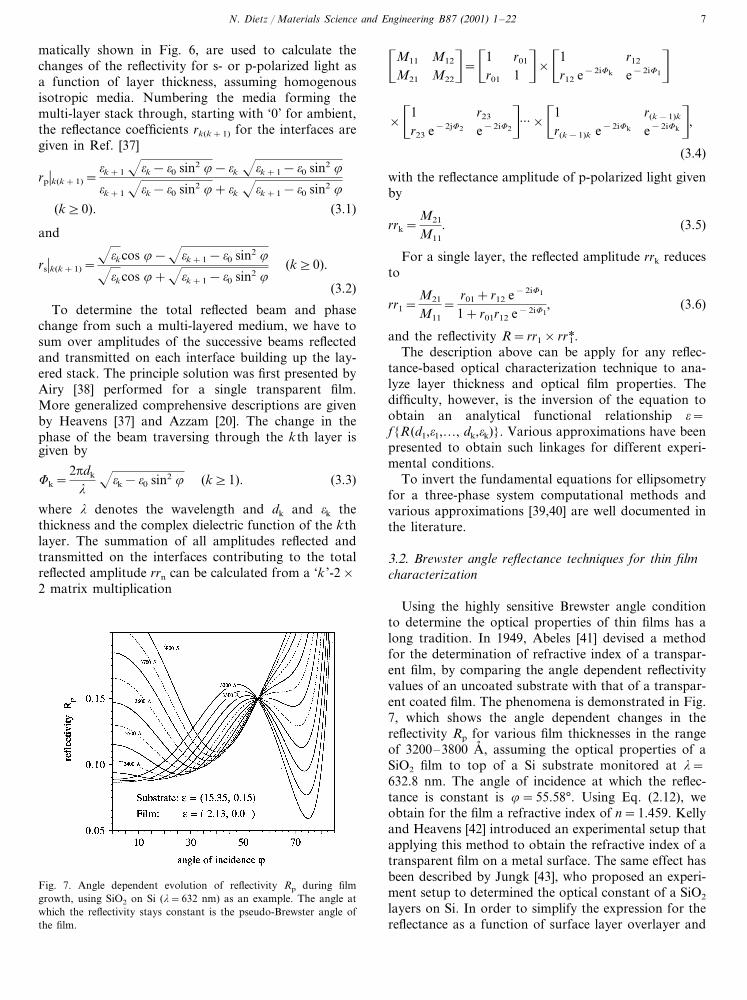
Using the highly sensitive Brewster angle conditionto determine the optical properties of thin films has along tradition. In 1949, Abeles [41] devised a methodfor the determination of refractive index of a transpar-ent film, by comparing the angle dependent reflectivityvalues of an uncoated substrate with that of a transpar-ent coated film. The phenomena is demonstrated in Fig.7, which shows the angle dependent changes in thereflectivity Rp for various film thicknesses in the rangeof 3200–3800 A� , assuming the optical properties of aSiO2 film to top of a Si substrate monitored at =632.8 nm. The angle of incidence at which the reflec-tance is constant is �=55.58°. Using Eq. (2.12), weobtain for the film a refractive index of n=1.459. Kellyand Heavens [42] introduced an experimental setup thatapplying this method to obtain the refractive index of atransparent film on a metal surface. The same effect hasbeen described by Jungk [43], who proposed an experi-ment setup to determined the optical constant of a SiO2
layers on Si. In order to simplify the expression for thereflectance as a function of surface layer overlayer and
Fig. 7. Angle dependent evolution of reflectivity Rp during filmgrowth, using SiO2 on Si ( =632 nm) as an example. The angle atwhich the reflectivity stays constant is the pseudo-Brewster angle ofthe film.
N. Dietz / Materials Science and Engineering B87 (2001) 1–228
�p, McIntyre and Aspnes [39,40] discussed theoreticallythe change in the reflectance, �R/R= (Rafs−Ras)/Ras,for thin surface layer (thickness dp� ) using a linearapproximation in the phase factor �f for a three layer(ambient/film/substrate) stack.
In 1973, A. Balzarotti et al. [44] proposed a methodthat analyzes the derivative dRp/d� around the pseudo-Brewster angle �B and presented approximated analyti-cal expressions for weak absorbent media. He alsopointed out the high sensitivity of his technique to-wards surface modifications and discussed the potentialuse of this technique to characterize surface layers.
The application towards determination of thicknessof organic layers on solid substrates has been describedby Arwin et al. [45,46].
However, the complexity of angle dependentFresnel’s equations made it almost impossible to for-mulate general analytical expressions that link the opti-cal materials properties to the measurement values,which restricted their use to special experimental appli-cation. Progress in the formulation of analytical rela-tions was made by Azzam et al., [35,54] and by thereadiness availability of computing power, which al-lowed the numerical analysis of the expressions. End ofthe 80th, Kobayashi et al. [13,47–51] utilized the sensi-tivity of p-polarized light in the vicinity near the Brew-ster angle towards real-time monitoring of surfacechemical composition during epitaxial GaAs growthusing metalorganic precursor. Their application focusedon the strong absorbing region of a compound semi-conductor in order to gain high sensitivity towardssurface processes. The technique was denoted accord-ingly as SPA. The theoretical interpretation of the SPAsignal has been described by Horikoshi et al. [52] andHingerl et al. [53], who calculated the changes in �R/Runder SPA conditions and provided the basis for de-tecting process-induced changes in surface chemicalcomposition by photo-absorption (SPA).
The concept of PRS was introduced through [17] andis based on the spectroscopic analysis of differences inthe dielectric functions of different media. Both, SPAand PRS, are utilizing the p-polarized light near thepseudo-Brewster angle of a medium to suppress thebulk reflectance component in favor to (near-) surfacecontributions. In contrast to SPA, which restricts itselfto the highly absorbent wavelength region, PRS isapplied in the transparent and weak absorbent wave-length range in order to analyze differences in thedielectric functions of different media. As shown inSection 3.1, each interface between two media gives riseto a complex reflectance coefficient and a with it con-tributes to the total reflected intensity. In a heterostruc-tural film growth process we have to consider aminimum of two interfaces: (a) ambient (�a=1) andfilm (�f�1), and (b) film (�f�1) and substrate (�s�1).Depending on the complexity of a heterostructure
stack, the number of interfaces contributing to thereflected intensity can become quite large, making itincreasing difficult to separate the various contribu-tions. A further complication arises from the fact thatnot only the differences in the dielectric functions, butalso the interface perfection enter as a parameter inreflectance coefficient for each interface.
The pseudo-Brewster angle law for an ideal interfacecan be formulated as a function of the complex opticalfunctions �. As shown in Section 1.2, the influence ofthe absorbing media on the Brewster angle can beexpressed as a shift in the angle �B at which and in anoffset, i.e. Rp��B
�0. For weakly absorbing media, thereflectivity Rp��
Blies in the order of 10−6–10−4 and
increases up to 10−2 for strong absorbing media, suchas metals. Assuming the growth of an ideal two-dimen-sional layer and a given dielectric function � of asubstrate, the reflected light from the surface can beinitially split in two contributions. One contributionrelated to the bulk properties of the substrate andsecond contribution due to the growing film. For anangle of incidence near the Brewster angle �B of thesubstrate, the bulk contribution strongly suppressedallowing highly sensitive detection of heterostructuralfilm nucleation and overgrowth processes. With this, ahigh surface sensitivity. The PRS configuration bychoice of an appropriate probe wavelength, informa-tion from Since. The richness of information obtainedin such a real-time growth monitoring is demonstrate inSection 3.3.
Further, changes in the growth conditions, such as avariation in the growth rate, density fluctuations orchanges in the optical function � during the growthresults in a change of the slope in the monitoredreflectance spectrum or in a discontinuity in the deriva-tive reflectance spectrum, respectively.
3.3. Thin film growth characterization by p-polarizedreflectance spectroscopy
Applying optical probe techniques towards real-timecharacterization of thin film growth, involving metalor-ganic precursors, inherits the challenge to relate surfacechemistry processes that drives the growth process,towards growth/film properties, such as composition,instantaneous growth rate or structural layer quality.Characterization and understanding of surface chem-istry processes requires the development of high sensi-tive methods to characterize growth, ideally at the pointwhere the growth process itself occurs and might becontrollable. Many of the present efforts are directedtowards accurately measuring ambient process parame-ters, such as pressure, flux or temperature, since numer-ous probes are available to provide a relative detailedassessment of the ambient. However, this strategy isclearly limited in its capability to deal with complex
N. Dietz / Materials Science and Engineering B87 (2001) 1–22 9
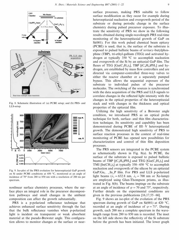
Fig. 8. Schematic illustration of: (a) PCBE setup; and (b) PRS- andLLS-setup.
surface processes, making PRS suitable to followsurface modification as they occur for example duringheteroepitaxial nucleation and overgrowth period of thesubstrate or during periodic change in the surfacechemistry during pulsed precursor exposure. To illus-trate the sensitivity of PRS we show in the followingresults obtained during single-wavelength PRS real-timemonitoring of the heteroepitaxial growth of GaP onSi(001). For this work pulsed chemical beam epitaxy(PCBE) is used, that is, the surface of the substrate isexposed to pulsed ballistic beams of tertiary-butylphos-phine (TBP), tri-ethyl-gallium (TEG) and activated hy-drogen at typically 350 °C to accomplish nucleationand overgrowth of the Si by an epitaxial GaP film. Thefluxes of TEG [Ga(C2H5)3], TBP [(C4H9)PH2] and hy-drogen, are established by mass flow controllers and aredirected via computer-controlled three-way valves toeither the reactor chamber or a separately pumpedbypass. This allows the sequential exposure of thesubstrate to individual pulses of the precursormolecules. The switching of the sources is synchronizedwith the data acquisition of the PRS and LLS signals tocorrelate changes in the reflected light intensity with thechanges in the optical properties of the heteroepitaxialstack and with changes in the thickness and opticalproperties of the epitaxial film.
Utilizing the high sensitivity of a Brewster anglecondition, we introduced PRS as an optical probetechnique for both, surface- and thin film characteriza-tion technique. Its sensitivity and capability has beendemonstrated during PCBE of III–V heteroepitaxialgrowth. The demonstrated high sensitivity of PRS tosurface reaction processes in the context of real-timemonitoring of PCBE has opened new possibilities forcharacterization and control of thin film depositionprocesses.
The PRS sensors are integrated in the PCBE systemas schematically shown in Fig. 8(a). In PCBE, thesurface of the substrate is exposed to pulsed ballisticbeams of TBP [(C4H9)PH2] and TEG [Ga(C2H5)3] andTMI [In(CH3)3] at typically 350–450 °C to accomplishnucleation and overgrowth of the silicon by an epitaxialGaP/Ga1−xInxP film. For PRS and LLS p-polarizedlight beams ( 1=632.8 nm, 2=700 nm or Xe-lamp)are employed using Glan-Thompson prisms, as illus-trated in Fig. 8(b). The beams impinge on the substrateat an angle of incidence of �=70 and 75°, respectively.Further details on the experimental conditions aregiven in the previous publications [16,17,55–66].
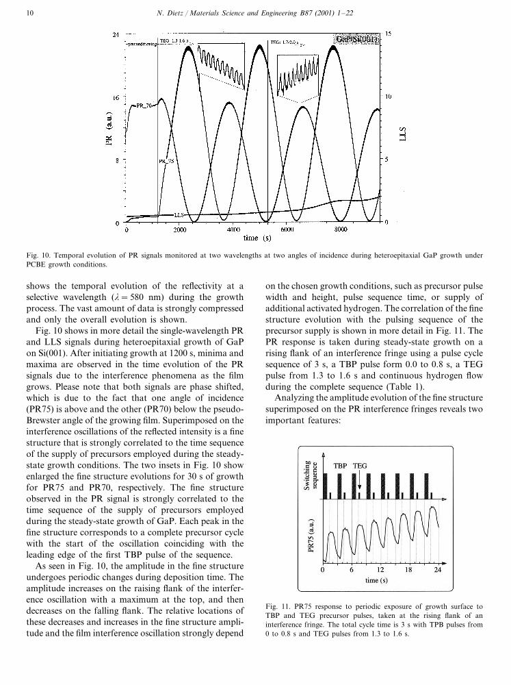
Fig. 9 shows an iso-plot of the evolution of the PRSspectrum during growth of GaP on Si(001) at 420 °C,recorded at an angle of incidence of �=71°. Duringgrowth, each 200 ms a complete spectrum in the wave-length range from 280 to 850 nm is recorded. The inseton the left side shows the reflectivity of the Si substratebefore the growth has been initiated. The lower graph
Fig. 9. Iso-plot of the PRS evolution for heteroepitaxial GaP growthon Si under PCBE conditions at 450 °C, monitored at an angle ofincidence of 70° from 280 to 850 nm with a resolution of 200 ms perspectrum.
nonlinear surface chemistry processes, where the sur-face plays an integral role in the precursor decomposi-tion pathways and small changes in the ambientcomposition can affect the growth substantially.
PRS is a p-polarized reflectance technique thatachieves enhanced surface sensitivity through the factthat the bulk reflectance vanishes when p-polarizedlight is incident on transparent or weak absorbentmaterial at the pseudo-Brewster angle. This configura-tion allows to monitor changes at the surface or near-
N. Dietz / Materials Science and Engineering B87 (2001) 1–2210
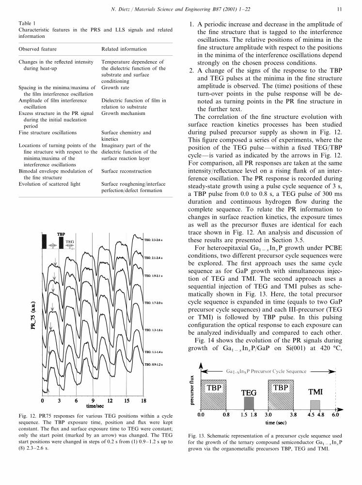
Fig. 10. Temporal evolution of PR signals monitored at two wavelengths at two angles of incidence during heteroepitaxial GaP growth underPCBE growth conditions.
shows the temporal evolution of the reflectivity at aselective wavelength ( =580 nm) during the growthprocess. The vast amount of data is strongly compressedand only the overall evolution is shown.
Fig. 10 shows in more detail the single-wavelength PRand LLS signals during heteroepitaxial growth of GaPon Si(001). After initiating growth at 1200 s, minima andmaxima are observed in the time evolution of the PRsignals due to the interference phenomena as the filmgrows. Please note that both signals are phase shifted,which is due to the fact that one angle of incidence(PR75) is above and the other (PR70) below the pseudo-Brewster angle of the growing film. Superimposed on theinterference oscillations of the reflected intensity is a finestructure that is strongly correlated to the time sequenceof the supply of precursors employed during the steady-state growth conditions. The two insets in Fig. 10 showenlarged the fine structure evolutions for 30 s of growthfor PR75 and PR70, respectively. The fine structureobserved in the PR signal is strongly correlated to thetime sequence of the supply of precursors employedduring the steady-state growth of GaP. Each peak in thefine structure corresponds to a complete precursor cyclewith the start of the oscillation coinciding with theleading edge of the first TBP pulse of the sequence.
As seen in Fig. 10, the amplitude in the fine structureundergoes periodic changes during deposition time. Theamplitude increases on the raising flank of the interfer-ence oscillation with a maximum at the top, and thendecreases on the falling flank. The relative locations ofthese decreases and increases in the fine structure ampli-tude and the film interference oscillation strongly depend
on the chosen growth conditions, such as precursor pulsewidth and height, pulse sequence time, or supply ofadditional activated hydrogen. The correlation of the finestructure evolution with the pulsing sequence of theprecursor supply is shown in more detail in Fig. 11. ThePR response is taken during steady-state growth on arising flank of an interference fringe using a pulse cyclesequence of 3 s, a TBP pulse form 0.0 to 0.8 s, a TEGpulse from 1.3 to 1.6 s and continuous hydrogen flowduring the complete sequence (Table 1).
Analyzing the amplitude evolution of the fine structuresuperimposed on the PR interference fringes reveals twoimportant features:
Fig. 11. PR75 response to periodic exposure of growth surface toTBP and TEG precursor pulses, taken at the rising flank of aninterference fringe. The total cycle time is 3 s with TPB pulses from0 to 0.8 s and TEG pulses from 1.3 to 1.6 s.
N. Dietz / Materials Science and Engineering B87 (2001) 1–22 11
Table 1Characteristic features in the PRS and LLS signals and relatedinformation
Related informationObserved feature
Changes in the reflected intensity Temperature dependence ofduring heat-up the dielectric function of the
substrate and surfaceconditioning
Spacing in the minima/maxima of Growth ratethe film interference oscillation
Dielectric function of film inAmplitude of film interferenceoscillation relation to substrate
Growth mechanismExcess structure in the PR signalduring the initial nucleationperiod
Surface chemistry andFine structure oscillationskineticsImaginary part of theLocations of turning points of the
fine structure with respect to the dielectric function of thesurface reaction layerminima/maxima of the
interference oscillationsSurface reconstructionBimodal envelope modulation of
the fine structureSurface roughening/interfaceEvolution of scattered lightperfection/defect formation
1. A periodic increase and decrease in the amplitude ofthe fine structure that is tagged to the interferenceoscillations. The relative positions of minima in thefine structure amplitude with respect to the positionsin the minima of the interference oscillations dependstrongly on the chosen process conditions.
2. A change of the signs of the response to the TBPand TEG pulses at the minima in the fine structureamplitude is observed. The (time) positions of theseturn-over points in the pulse response will be de-noted as turning points in the PR fine structure inthe further text.
The correlation of the fine structure evolution withsurface reaction kinetics processes has been studiedduring pulsed precursor supply as shown in Fig. 12.This figure composed a series of experiments, where theposition of the TEG pulse—within a fixed TEG/TBPcycle— is varied as indicated by the arrows in Fig. 12.For comparison, all PR responses are taken at the sameintensity/reflectance level on a rising flank of an inter-ference oscillation. The PR response is recorded duringsteady-state growth using a pulse cycle sequence of 3 s,a TBP pulse from 0.0 to 0.8 s, a TEG pulse of 300 msduration and continuous hydrogen flow during thecomplete sequence. To relate the PR information tochanges in surface reaction kinetics, the exposure timesas well as the precursor fluxes are identical for eachtrace shown in Fig. 12. An analysis and discussion ofthese results are presented in Section 3.5.
For heteroepitaxial Ga1−xInxP growth under PCBEconditions, two different precursor cycle sequences werebe explored. The first approach uses the same cyclesequence as for GaP growth with simultaneous injec-tion of TEG and TMI. The second approach uses asequential injection of TEG and TMI pulses as sche-matically shown in Fig. 13. Here, the total precursorcycle sequence is expanded in time (equals to two GaPprecursor cycle sequences) and each III-precursor (TEGor TMI) is followed by TBP pulse. In this pulsingconfiguration the optical response to each exposure canbe analyzed individually and compared to each other.
Fig. 14 shows the evolution of the PR signals duringgrowth of Ga1−xInxP/GaP on Si(001) at 420 °C,
Fig. 12. PR75 responses for various TEG positions within a cyclesequence. The TBP exposure time, position and flux were keptconstant. The flux and surface exposure time to TEG were constant;only the start point (marked by an arrow) was changed. The TEGstart positions were changed in steps of 0.2 s from (1) 0.9–1.2 s up to(8) 2.3–2.6 s.
Fig. 13. Schematic representation of a precursor cycle sequence usedfor the growth of the ternary compound semiconductor Ga1−xInxPgrown via the organometallic precursors TBP, TEG and TMI.
N. Dietz / Materials Science and Engineering B87 (2001) 1–2212
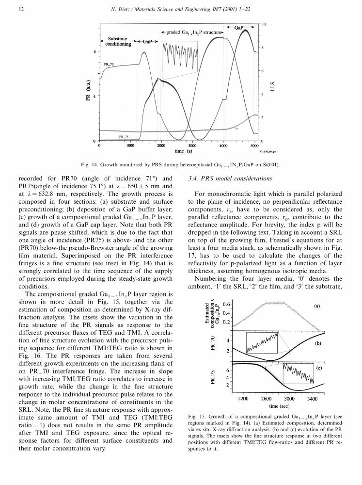
Fig. 14. Growth monitored by PRS during heteroepitasial Ga1−xINxP/GaP on Si(001).
recorded for PR70 (angle of incidence 71°) andPR75(angle of incidence 75.1°) at =650�5 nm andat =632.8 nm, respectively. The growth process iscomposed in four sections: (a) substrate and surfacepreconditioning; (b) deposition of a GaP buffer layer;(c) growth of a compositional graded Ga1−xInxP layer,and (d) growth of a GaP cap layer. Note that both PRsignals are phase shifted, which is due to the fact thatone angle of incidence (PR75) is above- and the other(PR70) below-the pseudo-Brewster angle of the growingfilm material. Superimposed on the PR interferencefringes is a fine structure (see inset in Fig. 14) that isstrongly correlated to the time sequence of the supplyof precursors employed during the steady-state growthconditions.
The compositional graded Ga1−xInxP layer region isshown in more detail in Fig. 15, together via theestimation of composition as determined by X-ray dif-fraction analysis. The insets show the variation in thefine structure of the PR signals as response to thedifferent precursor fluxes of TEG and TMI. A correla-tion of fine structure evolution with the precursor puls-ing sequence for different TMI:TEG ratio is shown inFig. 16. The PR responses are taken from severaldifferent growth experiments on the increasing flank ofon PR–70 interference fringe. The increase in slopewith increasing TMI:TEG ratio correlates to increase ingrowth rate, while the change in the fine structureresponse to the individual precursor pulse relates to thechange in molar concentrations of constituents in theSRL. Note, the PR fine structure response with approx-imate same amount of TMI and TEG (TMI:TEGratio=1) does not results in the same PR amplitudeafter TMI and TEG exposure, since the optical re-sponse factors for different surface constituents andtheir molar concentration vary.
3.4. PRS model considerations
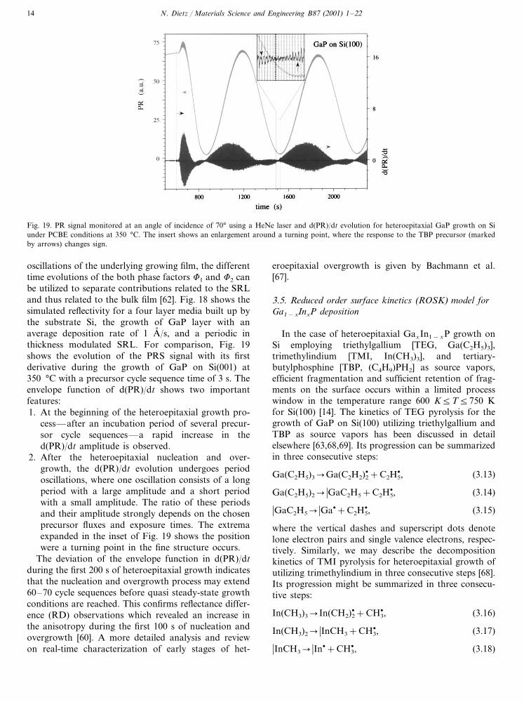
For monochromatic light which is parallel polarizedto the plane of incidence, no perpendicular reflectancecomponents, rs, have to be considered as, only theparallel reflectance components, rp, contribute to thereflectance amplitude. For brevity, the index p will bedropped in the following text. Taking in account a SRLon top of the growing film, Fresnel’s equations for atleast a four media stack, as schematically shown in Fig.17, has to be used to calculate the changes of thereflectivity for p-polarized light as a function of layerthickness, assuming homogenous isotropic media.
Numbering the four layer media, ‘0’ denotes theambient, ‘1’ the SRL, ‘2’ the film, and ‘3’ the substrate,
Fig. 15. Growth of a compositional graded Ga1−xInxP layer (seeregions marked in Fig. 14). (a) Estimated composition, determinedvia ex-situ X-ray diffraction analysis. (b) and (c) evolution of the PRsignals. The insets show the fine structure response at two differentpositions with different TMI:TEG flow-ratios and different PR re-sponses to it.
N. Dietz / Materials Science and Engineering B87 (2001) 1–22 13
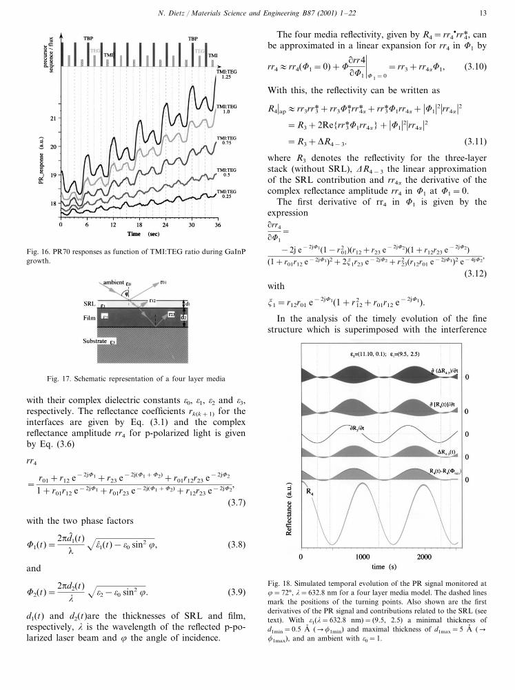
Fig. 16. PR70 responses as function of TMI:TEG ratio during GaInPgrowth.
The four media reflectivity, given by R4=rr4�rr4*, can
be approximated in a linear expansion for rr4 in �1 by
rr4�rr4(�1=0)+��rr4��1
�� 1=0
=rr3+rr4��1, (3.10)
With this, the reflectivity can be written as
R4�ap�rr3rr3*+rr3�1*rr4�* +rr3*�1rr4�+ ��1�2�rr4� �2=R3+2Re{rr3*�1rr4�}+ ��1�2�rr4� �2=R3+�R4−3. (3.11)
where R3 denotes the reflectivity for the three-layerstack (without SRL), �R4−3 the linear approximationof the SRL contribution and rr4� the derivative of thecomplex reflectance amplitude rr4 in �1 at �1=0.
The first derivative of rr4 in �1 is given by theexpression�rr4
��1
=
−2j e−2j�1(1−r012 )(r12+r23 e−2j�2)(1+r12r23 e−2j�2)
(1+r01r12 e−2j�1)2+2�1r23 e−2j�2+r232 (r12r01 e−2j�1)2 e−4j�2
,
(3.12)with
�1=r12r01 e−2j�1(1+r122 +r01r12 e−2j�1).
In the analysis of the timely evolution of the finestructure which is superimposed with the interference
Fig. 17. Schematic representation of a four layer media
Fig. 18. Simulated temporal evolution of the PR signal monitored at�=72°, =632.8 nm for a four layer media model. The dashed linesmark the positions of the turning points. Also shown are the firstderivatives of the PR signal and contributions related to the SRL (seetext). With �1( =632.8 nm)= (9.5, 2.5) a minimal thickness ofd1min=0.5 A� (��1min) and maximal thickness of d1max=5 A� (��1max), and an ambient with �0=1.
with their complex dielectric constants �0, �1, �2 and �3,respectively. The reflectance coefficients rk(k+1) for theinterfaces are given by Eq. (3.1) and the complexreflectance amplitude rr4 for p-polarized light is givenby Eq. (3.6)
rr4
=r01+r12 e−2j�1+r23 e−2j(�1+�2)+r01r12r23 e−2j�2
1+r01r12 e−2j�1+r01r23 e−2j(�1+�2)+r12r23 e−2j�2,
(3.7)
with the two phase factors
�1(t)=2�d� 1(t)
���1(t)−�0 sin2 �, (3.8)
and
�2(t)=2�d2(t)
��2−�0 sin2 �. (3.9)
d1(t) and d2(t)are the thicknesses of SRL and film,respectively, is the wavelength of the reflected p-po-larized laser beam and � the angle of incidence.
N. Dietz / Materials Science and Engineering B87 (2001) 1–2214
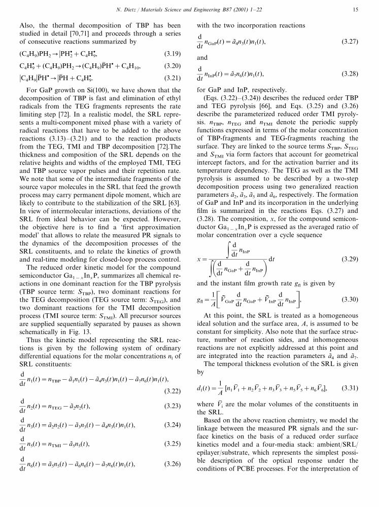
Fig. 19. PR signal monitored at an angle of incidence of 70° using a HeNe laser and d(PR)/dt evolution for heteroepitaxial GaP growth on Siunder PCBE conditions at 350 °C. The insert shows an enlargement around a turning point, where the response to the TBP precursor (markedby arrows) changes sign.
oscillations of the underlying growing film, the differenttime evolutions of the both phase factors �1 and �2 canbe utilized to separate contributions related to the SRLand thus related to the bulk film [62]. Fig. 18 shows thesimulated reflectivity for a four layer media built up bythe substrate Si, the growth of GaP layer with anaverage deposition rate of 1 A� /s, and a periodic inthickness modulated SRL. For comparison, Fig. 19shows the evolution of the PRS signal with its firstderivative during the growth of GaP on Si(001) at350 °C with a precursor cycle sequence time of 3 s. Theenvelope function of d(PR)/dt shows two importantfeatures:1. At the beginning of the heteroepitaxial growth pro-
cess—after an incubation period of several precur-sor cycle sequences—a rapid increase in thed(PR)/dt amplitude is observed.
2. After the heteroepitaxial nucleation and over-growth, the d(PR)/dt evolution undergoes periodoscillations, where one oscillation consists of a longperiod with a large amplitude and a short periodwith a small amplitude. The ratio of these periodsand their amplitude strongly depends on the chosenprecursor fluxes and exposure times. The extremaexpanded in the inset of Fig. 19 shows the positionwere a turning point in the fine structure occurs.
The deviation of the envelope function in d(PR)/dtduring the first 200 s of heteroepitaxial growth indicatesthat the nucleation and overgrowth process may extend60–70 cycle sequences before quasi steady-state growthconditions are reached. This confirms reflectance differ-ence (RD) observations which revealed an increase inthe anisotropy during the first 100 s of nucleation andovergrowth [60]. A more detailed analysis and reviewon real-time characterization of early stages of het-
eroepitaxial overgrowth is given by Bachmann et al.[67].
3.5. Reduced order surface kinetics (ROSK) model forGa1−xInxP deposition
In the case of heteroepitaxial GaxIn1−xP growth onSi employing triethylgallium [TEG, Ga(C2H5)3],trimethylindium [TMI, In(CH3)3], and tertiary-butylphosphine [TBP, (C4H9)PH2] as source vapors,efficient fragmentation and sufficient retention of frag-ments on the surface occurs within a limited processwindow in the temperature range 600 KT750 Kfor Si(100) [14]. The kinetics of TEG pyrolysis for thegrowth of GaP on Si(100) utilizing triethylgallium andTBP as source vapors has been discussed in detailelsewhere [63,68,69]. Its progression can be summarizedin three consecutive steps:
Ga(C2H5)3�Ga(C2H2)2�+C2H5
�, (3.13)
Ga(C2H5)2� �GaC2H5+C2H5�, (3.14)
�GaC2H5� �Ga�+C2H5�, (3.15)
where the vertical dashes and superscript dots denotelone electron pairs and single valence electrons, respec-tively. Similarly, we may describe the decompositionkinetics of TMI pyrolysis for heteroepitaxial growth ofutilizing trimethylindium in three consecutive steps [68].Its progression might be summarized in three consecu-tive steps:
In(CH3)3�In(CH2)2�+CH3
�, (3.16)
In(CH3)2� �InCH3+CH3�, (3.17)
�InCH3� �In�+CH3�, (3.18)
N. Dietz / Materials Science and Engineering B87 (2001) 1–22 15
Also, the thermal decomposition of TBP has beenstudied in detail [70,71] and proceeds through a seriesof consecutive reactions summarized by
(C4H9)PH2� �PH2�+C4H9
�, (3.19)
C4H9�+ (C4H9)PH2� (C4H9)P� H�+C4H10, (3.20)
�C4H9�P� H�� �P� H+C4H9�. (3.21)
For GaP growth on Si(100), we have shown that thedecomposition of TBP is fast and elimination of ethylradicals from the TEG fragments represents the ratelimiting step [72]. In a realistic model, the SRL repre-sents a multi-component mixed phase with a variety ofradical reactions that have to be added to the abovereactions (3.13)– (3.21) and to the reaction productsfrom the TEG, TMI and TBP decomposition [72].Thethickness and composition of the SRL depends on therelative heights and widths of the employed TMI, TEGand TBP source vapor pulses and their repetition rate.We note that some of the intermediate fragments of thesource vapor molecules in the SRL that feed the growthprocess may carry permanent dipole moment, which arelikely to contribute to the stabilization of the SRL [63].In view of intermolecular interactions, deviations of theSRL from ideal behavior can be expected. However,the objective here is to find a ‘first approximationmodel’ that allows to relate the measured PR signals tothe dynamics of the decomposition processes of theSRL constituents, and to relate the kinetics of growthand real-time modeling for closed-loop process control.
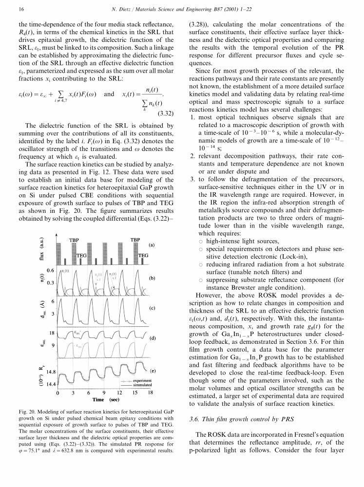
The reduced order kinetic model for the compoundsemiconductor Ga1−xInxP, summarizes all chemical re-actions in one dominant reaction for the TBP pyrolysis(TBP source term: STBP), two dominant reactions forthe TEG decomposition (TEG source term: STEG), andtwo dominant reactions for the TMI decompositionprocess (TMI source term: STMI). All precursor sourcesare supplied sequentially separated by pauses as shownschematically in Fig. 13.
Thus the kinetic model representing the SRL reac-tions is given by the following system of ordinarydifferential equations for the molar concentrations nl ofSRL constituents:
ddt
n1(t)=nTBP− a1n1(t)− a4n3(t)n1(t)− a7n6(t)n1(t),
(3.22)
ddt
n2(t)=nTEG− a2n2(t), (3.23)
ddt
n3(t)= a2n2(t)− a3n3(t)− a4n3(t)n1(t), (3.24)
ddt
n5(t)=nTMI− a5n5(t), (3.25)
ddt
n6(t)= a5n5(t)− a6n6(t)− a7n6(t)n1(t), (3.26)
with the two incorporation reactions
ddt
nGaP(t)= a4n3(t)n1(t), (3.27)
and
ddt
nInP(t)= a7n6(t)n1(t), (3.28)
for GaP and InP, respectively.(Eqs. (3.22)– (3.24)) describes the reduced order TBP
and TEG pyrolysis [66], and Eqs. (3.25) and (3.26)describe the parameterized reduced order TMI pyroly-sis. nTBP, nTEG and nTMI denote the periodic supplyfunctions expressed in terms of the molar concentrationof TBP-fragments and TEG-fragments reaching thesurface. They are linked to the source terms STBP, STEG
and STMI via form factors that account for geometricalintercept factors, and for the activation barrier and itstemperature dependency. The TEG as well as the TMIpyrolysis is assumed to be described by a two-stepdecomposition process using two generalized reactionparameters a2, a3, a5 and a6, respectively. The formationof GaP and InP and its incorporation in the underlyingfilm is summarized in the reactions Eqs. (3.27) and(3.28). The composition, x, for the compound semicon-ductor Ga1−xInxP is expressed as the averaged ratio ofmolar concentration over a cycle sequence
x=
ddt
nInP� ddt
nGaP+ddt
nInP� dt (3.29)
and the instant film growth rate gfl is given by
gfl=1A�
V� GaP
ddt
nGaP+V� InP
ddt
nInPn
, (3.30)
At this point, the SRL is treated as a homogeneousideal solution and the surface area, A, is assumed to beconstant for simplicity. Also note that the surface struc-ture, number of reaction sides, and inhomogeneousreactions are not explicitly addressed at this point andare integrated into the reaction parameters a4 and a7.
The temporal thickness evolution of the SRL is givenby
d1(t)=1A
[n1V� 1+n2V� 2+n3V� 3+n5V� 5+n6V� 6], (3.31)
where V� i are the molar volumes of the constituents inthe SRL.
Based on the above reaction chemistry, we model thelinkage between the measured PR signals and the sur-face kinetics on the basis of a reduced order surfacekinetics model and a four-media stack: ambient/SRL/epilayer/substrate, which represents the simplest possi-ble description of the optical response under theconditions of PCBE processes. For the interpretation of
N. Dietz / Materials Science and Engineering B87 (2001) 1–2216
the time-dependence of the four media stack reflectance,R4(t), in terms of the chemical kinetics in the SRL thatdrives epitaxial growth, the dielectric function of theSRL, �1, must be linked to its composition. Such a linkagecan be established by approximating the dielectric func-tion of the SRL through an effective dielectric function�1, parameterized and expressed as the sum over all molarfractions xi contributing to the SRL:
�i(�)=�+ �i�4,7
xi(t)Fi(�) and xi(t)=ni(t)
�k
nk(t).
(3.32)
The dielectric function of the SRL is obtained bysumming over the contributions of all its constituents,identified by the label i. Fi(�) in Eq. (3.32) denotes theoscillator strength of the transitions and � denotes thefrequency at which �1 is evaluated.
The surface reaction kinetics can be studied by analyz-ing data as presented in Fig. 12. These data were usedto establish an initial data base for modeling of thesurface reaction kinetics for heteroepitaxial GaP growthon Si under pulsed CBE conditions with sequentialexposure of growth surface to pulses of TBP and TEGas shown in Fig. 20. The figure summarizes resultsobtained by solving the coupled differential (Eqs. (3.22)–
(3.28)), calculating the molar concentrations of thesurface constituents, their effective surface layer thick-ness and the dielectric optical properties and comparingthe results with the temporal evolution of the PRresponse for different precursor fluxes and cycle se-quences.
Since for most growth processes of the relevant, thereactions pathways and their rate constants are presentlynot known, the establishment of a more detailed surfacekinetics model and validating data by relating real-timeoptical and mass spectroscopic signals to a surfacereactions kinetics model has several challenges:1. most optical techniques observe signals that are
related to a macroscopic description of growth witha time-scale of 10−3–10−6 s, while a molecular-dy-namic models of growth are a time-scale of 10−12–10−14 s;
2. relevant decomposition pathways, their rate con-stants and temperature dependence are not knownor are under dispute and
3. to follow the defragmentation of the precursors,surface-sensitive techniques either in the UV or inthe IR wavelength range are required. However, inthe IR region the infra-red absorption strength ofmetalalkyls source compounds and their defragmen-tation products are two to three orders of magni-tude lower than in the visible wavelength range,which requires:� high-intense light sources,� special requirements on detectors and phase sen-
sitive detection electronic (Lock-in),� reducing infrared radiation from a hot substrate
surface (tunable notch filters) and� suppressing substrate reflectance component (for
instance Brewster angle condition).However, the above ROSK model provides a de-
scription as how to relate changes in composition andthickness of the SRL to an effective dielectric function�1(�,t) and, d1(t), respectively. With this, the instanta-neous composition, x, and growth rate gfl(t) for thegrowth of GaxIn1−xP heterostructures under closed-loop feedback, as demonstrated in Section 3.6. For thinfilm growth control, a data base for the parameterestimation for Ga1−xInxP growth has to be establishedand fast filtering and feedback algorithms have to bedeveloped to close the real-time feedback-loop. Eventhough some of the parameters involved, such as themolar volumes and optical oscillator strengths can beestimated, a larger set of experimental data are requiredto validate the analysis of surface reaction kinetics.
3.6. Thin film growth control by PRS
The ROSK data are incorporated in Fresnel’s equationthat determines the reflectance amplitude, rr, of thep-polarized light as follows. Consider the four layer
Fig. 20. Modeling of surface reaction kinetics for heteroepitaxial GaPgrowth on Si under pulsed chemical beam epitaxy conditions withsequential exposure of growth surface to pulses of TBP and TEG.The molar concentrations of the surface constituents, their effectivesurface layer thickness and the dielectric optical properties are com-puted using (Eqs. (3.22)– (3.32)). The simulated PR response for�=75.1° and =632.8 nm is compared with experimental results.
N. Dietz / Materials Science and Engineering B87 (2001) 1–22 17
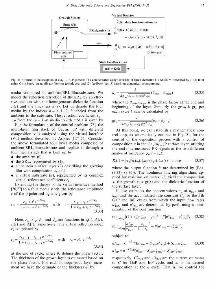
Fig. 21. Control of heteroepitaxial Ga1−xInxP growth: The compensator design consists of three elements: (1) ROSKM described by f ; (2) filtergains Gi(t) based on nonlinear-filtering techniques; and (3) feedback law K based on dynamical programming.
media composed of ambient/SRL/film/substrate. Wemodel the reflection/refraction of the SRL by an effec-tive medium with the homogeneous dielectric function�1(t) and the thickness d1(t). Let us denote the fourmedia by the indices n=0, 1, 2, 3 labeled from theambient to the substrate. The reflection coefficient rn−
1,n from the (n−1)-st media to nth media is given byFor the formulation of the control problem [73], the
multi-layer film stack of GaxIn1−xP with differentcomposition x is analyzed using the virtual interface(V-I) method described by Aspnes [1,74,75]. Considerthe above formulated four layer media composed ofambient/SRL/film/substrate and replace it through afour media stack that is built up by� the ambient (0),� the SRL, represented by (1),� a the near surface layer (2) describing the growing
film with composition x, and� a virtual substrate (k), represented by its complex
virtual reflectance coefficients rk.Extending the theory of the virtual interface method
[76,77] to a four media stack, the reflectance amplituder of the p-polarized light is given by
rr4=r01+ r e−2i�1
1+r01+ r e−2i�1with r=
r12+rk e−2i�2
1+r12+rk e−2i�2
(3.33)
Here, r01, r12, �1, and �2 are functions in �1(t), d1(t),�2(t) and d2(t), respectively. The virtual reflection indexrk is updated by
rk=rk,k−1−rk−1 e−2i�2
1+rk,k−1rk−1 e−2i�2with rk=Ak e− i�k
(3.34)
at the end of cycle, where �k defines the phase factor.The thickness of the grown layer is estimated based onthe phase factor. For each homogeneous layer incre-ment we have the estimate of the thickness d2 by
d2=
4���2−�0 sin2 �0
(�end−�begin) (3.35)
where the �end, �begin is the phase factor at the end andbeginning of the layer. Similarly the growth grk pereach cycle k can be calculated by
grk=
4���2−�0 sin2 �0
(�k−�k−1) (3.36)
At this point, we can establish a mathematical con-trol-loop, as schematically outlined in Fig. 21, for thecontrol of the deposition process with a control ofcomposition x in the GaxIn1−xP surface layer, utilizingthe real-time measured PR signals at the two differentangles of incidence �i, i=1,2:
Ri(t)= �rr4�2hi(�1(t),d1(t),gr(t),x(t)+noise (3.37)
where the output function hi are determined by (Eqs.(3.33)– (3.36)). The nonlinear filtering algorithms ap-plied for real-time estimates [78] yield the compositionx, the growth rate gr(t) and the dielectric function ofthe surface layer.
It also estimates the concentrations nk of nGaP andnInP and the accumulated rate constant Ck for the kthGaP and InP cycles from which the input flow ratesuTEG
k and uTMIk are determined by performing a mini-
mization of the cost function
minu TEGk �(1+zk)nGaP
+ −grd �2+� �uTEGk −uTEG
k−1�2, (3.38)
minu TMIk
�n InP+
nGaP+ −
zk
1−zk
�2+� �uTMI
k −uTMIk−1�2,
subject to
nGaP+ =e−CTEG
k
(nGaPc −SGaPuTEG
k )+SGaPuTEGk , (3.39)
n InP+ =e−CTMI
k
(n InPc −SInPuTMI
k )+SInPuTMIk ,
respectively. CTEGk and CTMI
k are the current estimatesof C for GaP and InP cycle, and zk is the desiredcomposition at the k cycle. That is, we control the
N. Dietz / Materials Science and Engineering B87 (2001) 1–2218
growth rate by uTEG and then by uTMI the compositionfor each cycle.
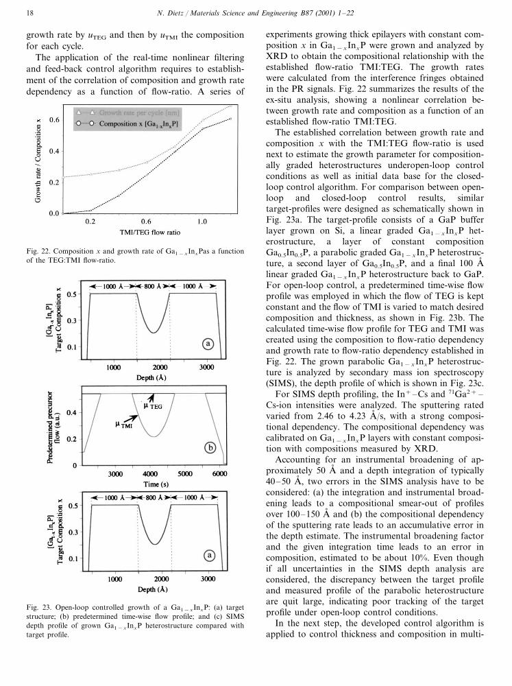
The application of the real-time nonlinear filteringand feed-back control algorithm requires to establish-ment of the correlation of composition and growth ratedependency as a function of flow-ratio. A series of
experiments growing thick epilayers with constant com-position x in Ga1−xInxP were grown and analyzed byXRD to obtain the compositional relationship with theestablished flow-ratio TMI:TEG. The growth rateswere calculated from the interference fringes obtainedin the PR signals. Fig. 22 summarizes the results of theex-situ analysis, showing a nonlinear correlation be-tween growth rate and composition as a function of anestablished flow-ratio TMI:TEG.
The established correlation between growth rate andcomposition x with the TMI:TEG flow-ratio is usednext to estimate the growth parameter for composition-ally graded heterostructures underopen-loop controlconditions as well as initial data base for the closed-loop control algorithm. For comparison between open-loop and closed-loop control results, similartarget-profiles were designed as schematically shown inFig. 23a. The target-profile consists of a GaP bufferlayer grown on Si, a linear graded Ga1−xInxP het-erostructure, a layer of constant compositionGa0.5In0.5P, a parabolic graded Ga1−xInxP heterostruc-ture, a second layer of Ga0.5In0.5P, and a final 100 A�linear graded Ga1−xInxP heterostructure back to GaP.For open-loop control, a predetermined time-wise flowprofile was employed in which the flow of TEG is keptconstant and the flow of TMI is varied to match desiredcomposition and thickness, as shown in Fig. 23b. Thecalculated time-wise flow profile for TEG and TMI wascreated using the composition to flow-ratio dependencyand growth rate to flow-ratio dependency established inFig. 22. The grown parabolic Ga1−xInxP heterostruc-ture is analyzed by secondary mass ion spectroscopy(SIMS), the depth profile of which is shown in Fig. 23c.
For SIMS depth profiling, the In+–Cs and 71Ga2+ –Cs-ion intensities were analyzed. The sputtering ratedvaried from 2.46 to 4.23 A� /s, with a strong composi-tional dependency. The compositional dependency wascalibrated on Ga1−xInxP layers with constant composi-tion with compositions measured by XRD.
Accounting for an instrumental broadening of ap-proximately 50 A� and a depth integration of typically40–50 A� , two errors in the SIMS analysis have to beconsidered: (a) the integration and instrumental broad-ening leads to a compositional smear-out of profilesover 100–150 A� and (b) the compositional dependencyof the sputtering rate leads to an accumulative error inthe depth estimate. The instrumental broadening factorand the given integration time leads to an error incomposition, estimated to be about 10%. Even thoughif all uncertainties in the SIMS depth analysis areconsidered, the discrepancy between the target profileand measured profile of the parabolic heterostructureare quit large, indicating poor tracking of the targetprofile under open-loop control conditions.
In the next step, the developed control algorithm isapplied to control thickness and composition in multi-
Fig. 22. Composition x and growth rate of Ga1−xInxPas a functionof the TEG:TMI flow-ratio.
Fig. 23. Open-loop controlled growth of a Ga1−xInxP: (a) targetstructure; (b) predetermined time-wise flow profile; and (c) SIMSdepth profile of grown Ga1−xInxP heterostructure compared withtarget profile.
N. Dietz / Materials Science and Engineering B87 (2001) 1–22 19
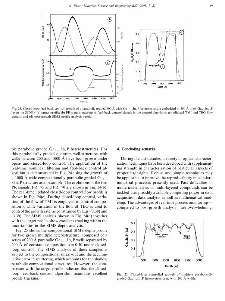
Fig. 24. Closed-loop feed-back control growth of a parabolic graded 600 A� wide Ga1−xInxP heterostructure embedded in 500 A� thick Ga0.5In0.5Players on Si(001): (a) target profile; (b) PR signals entering as feed-back control signals in the control algorithm; (c) adjusted TMI and TEG flowsignals; and (d) post-growth SIMS profile analysis result.
ple parabolic graded Ga1−xInxP heterostructures. Forthis parabolically graded quantum well structures withwells between 200 and 1000 A� have been grown underopen- and closed-loop control. The application of thereal-time nonlinear filtering and feed-back control al-gorithm is demonstrated in Fig. 24 using the growth ofa 1000 A� wide compositionally parabolic graded Ga1−
xInxP structure as an example. The evolutions of the twoPR signals, PR–75 and PR–70 are shown in Fig. 24(b).The real-time updated closed-loop control flow profile isshown in Fig. 24(c). During closed-loop control, varia-tion of the flow of TMI is employed to control compo-sition x while variation in the flow of TEG is used tocontrol the growth rate, as constrained by Eqs. (3.38) and(3.39). The SIMS analysis, shown in Fig. 24(d) togetherwith the target profile show excellent tracking within theuncertainties in the SIMS depth analysis.
Fig. 25 shows the compositional SIMS depth profilefor two grown multiple heterostructure, composed of aseries of 200 A� parabolic Ga1−xInxP wells separated by200 A� of constant composition x=0.40 under closed-loop control. The SIMS analysis of these samples issubject to the compositional smear-out and the accumu-lative error in sputtering, which accounts for the shallowparabolic compositional structures. However, the com-parison with the target profile indicates that the closed-loop feed-back control algorithm maintains excellentprofile tracking.
4. Concluding remarks
During the last decades, a variety of optical character-ization techniques have been developed with supplement-ing strength in characterization of particular aspects ofproperties/insights. Robust and simple techniques maybe applicable to improve the reproducibility in standardindustrial processes presently used. Past difficulties innumerical analysis of multi-layered compounds can betackled using readily available computing power in dataacquisition, data analysis as well as mathematical mod-eling. The advantages of real-time process monitoring—compared to post-growth analysis—are overwhelming,
Fig. 25. Closed-loop controlled growth of multiple parabolicallygraded Ga1−xInxP hetero-structures, with 200 A� width.
N. Dietz / Materials Science and Engineering B87 (2001) 1–2220
Fig. 26. Real-time monitoring of thin film growth applied in various regions relevant to the growth process.
considering the physical and chemical insights gainedand the opportunities opened up for process optimiza-tion and control.
The need of more complex characterization tech-niques with enhanced sensitivity to surface processeswill be largely focus to the following areas:� optimization of existing materials, heterostructures
and growth processes,� generation of precise recipe parameter that can be
transferred to industrial processes,� development of new materials, and� to gain a better understanding in fundamental physi-
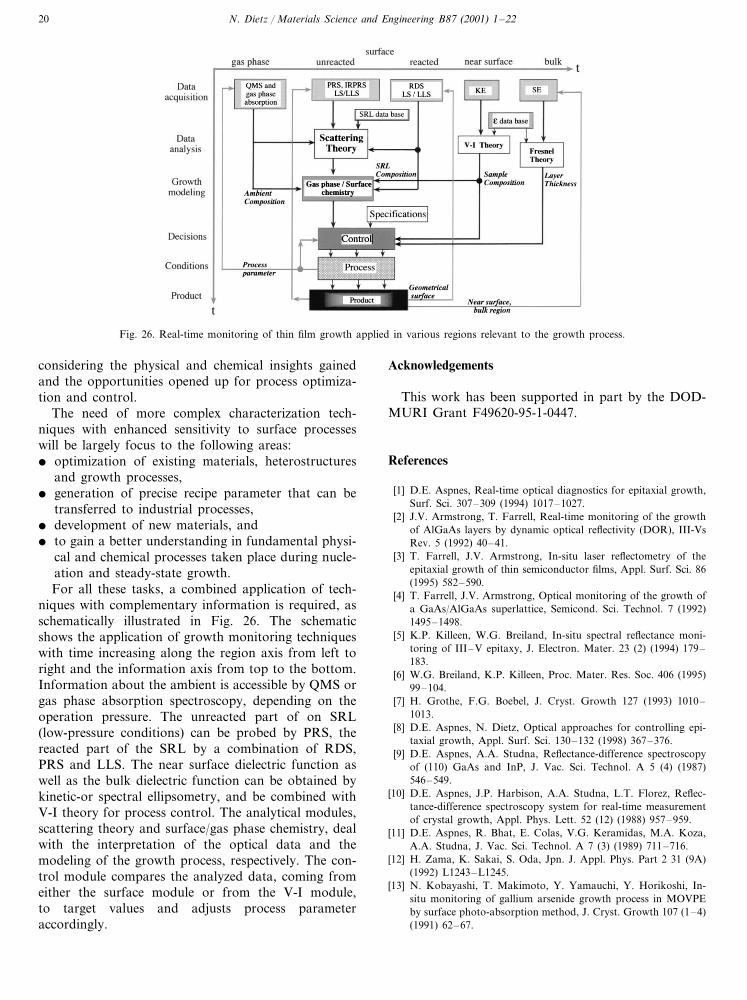
cal and chemical processes taken place during nucle-ation and steady-state growth.For all these tasks, a combined application of tech-
niques with complementary information is required, asschematically illustrated in Fig. 26. The schematicshows the application of growth monitoring techniqueswith time increasing along the region axis from left toright and the information axis from top to the bottom.Information about the ambient is accessible by QMS orgas phase absorption spectroscopy, depending on theoperation pressure. The unreacted part of on SRL(low-pressure conditions) can be probed by PRS, thereacted part of the SRL by a combination of RDS,PRS and LLS. The near surface dielectric function aswell as the bulk dielectric function can be obtained bykinetic-or spectral ellipsometry, and be combined withV-I theory for process control. The analytical modules,scattering theory and surface/gas phase chemistry, dealwith the interpretation of the optical data and themodeling of the growth process, respectively. The con-trol module compares the analyzed data, coming fromeither the surface module or from the V-I module,to target values and adjusts process parameteraccordingly.
Acknowledgements
This work has been supported in part by the DOD-MURI Grant F49620-95-1-0447.
References
[1] D.E. Aspnes, Real-time optical diagnostics for epitaxial growth,Surf. Sci. 307–309 (1994) 1017–1027.
[2] J.V. Armstrong, T. Farrell, Real-time monitoring of the growthof AlGaAs layers by dynamic optical reflectivity (DOR), III-VsRev. 5 (1992) 40–41.
[3] T. Farrell, J.V. Armstrong, In-situ laser reflectometry of theepitaxial growth of thin semiconductor films, Appl. Surf. Sci. 86(1995) 582–590.
[4] T. Farrell, J.V. Armstrong, Optical monitoring of the growth ofa GaAs/AlGaAs superlattice, Semicond. Sci. Technol. 7 (1992)1495–1498.
[5] K.P. Killeen, W.G. Breiland, In-situ spectral reflectance moni-toring of III–V epitaxy, J. Electron. Mater. 23 (2) (1994) 179–183.
[6] W.G. Breiland, K.P. Killeen, Proc. Mater. Res. Soc. 406 (1995)99–104.
[7] H. Grothe, F.G. Boebel, J. Cryst. Growth 127 (1993) 1010–1013.
[8] D.E. Aspnes, N. Dietz, Optical approaches for controlling epi-taxial growth, Appl. Surf. Sci. 130–132 (1998) 367–376.
[9] D.E. Aspnes, A.A. Studna, Reflectance-difference spectroscopyof (110) GaAs and InP, J. Vac. Sci. Technol. A 5 (4) (1987)546–549.
[10] D.E. Aspnes, J.P. Harbison, A.A. Studna, L.T. Florez, Reflec-tance-difference spectroscopy system for real-time measurementof crystal growth, Appl. Phys. Lett. 52 (12) (1988) 957–959.
[11] D.E. Aspnes, R. Bhat, E. Colas, V.G. Keramidas, M.A. Koza,A.A. Studna, J. Vac. Sci. Technol. A 7 (3) (1989) 711–716.
[12] H. Zama, K. Sakai, S. Oda, Jpn. J. Appl. Phys. Part 2 31 (9A)(1992) L1243–L1245.
[13] N. Kobayashi, T. Makimoto, Y. Yamauchi, Y. Horikoshi, In-situ monitoring of gallium arsenide growth process in MOVPEby surface photo-absorption method, J. Cryst. Growth 107 (1–4)(1991) 62–67.
N. Dietz / Materials Science and Engineering B87 (2001) 1–22 21
[14] T. Makimoto, Y. Yamauchi, N. Kobayashi, Y. Horikoshi, Jpn.J. Appl. Phys. 29 (2) (1990) L207–L209.
[15] N. Dietz, H.J. Lewerenz, An optical in-situ method for layergrowth characterization, Appl. Surf. Sci. 69 (1993) 350–354.
[16] N. Dietz, A. Miller, K.J. Bachmann, Real-time monitoring ofhomoepitaxial and heteroepitaxial processes by p-polarizedreflectance spectroscopy, J. Vac. Sci. Technol. A 13 (1995)153–155.
[17] N. Dietz, K.J. Bachmann, Real-time monitoring of epitaxialprocesses by parallel-polarized reflectance spectroscopy, MRSBull. 20 (1995) 49.
[18] K.A. Bertness, C. Kramer, J.M. Olson, J. Moreland, In-situobservation of surface morphology of InP grown on singularand vicinal (001) substrates, J. Electron. Mater. 23 (2) (1994)195.
[19] Max Born, Emil Wolf, Principles of Optics, 6th ed., Pergamon,New York, 1980.
[20] R.M.A. Azzam, N.M. Bashara, Ellipsometry and PolarizedLight, North-Holland, Amsterdam, ISBN 0-444-87016-4 (1987).
[21] I.P. Herman, Optical Diagnostics for thin Film Processing,Academic Press, New York, 1996.
[22] G. Bauer, W. Richter, Optical Characterization of EpitaxialSemiconductor Layers, Springer, Berlin, 1996.
[23] R.M.A. Azzam, Relationship between the p and s Fresnel reflec-tion coefficients of an interface independent of angle of inci-dence, Opt. Soc. Am. A 8 (7) (1986) 928–929.
[24] D. Brewster, A treatise on new philosophical instruments, vol.309, London, 1813.
[25] P.H. Miller, J.R. Johnson, Complex index of refraction ofsemiconducting surfaces, Physica XX (11) (1954) 1026–1028.
[26] S.P.F.b.t.l. Humphreys-Owen, Comparison of reflection methodsof measuring optical constants without polimetric analysis, andproposal for new methods based on the Brewster angle, Proc.Phys. Soc. LXXXVII 5 77, 1961, pp. 949–957.
[27] N. Dietz, H.J. Lewerenz, Simulataneous detection of opticalconstants �1 and �2 by Brewster angle reflectivity measurements,Appl. Phys. Lett. 60 (19) (1992) 2403.
[28] H.B. Holl, Specular reflexion and characteristics of reflectedlight, J. Opt. Soc. Am. 57 (1967) 683.
[29] R.F. Potter, Basic parameters for measuring optical properties,in: E.D. Palik (Ed.), Handbook of Optical Constants of Solids,Academic Press, Washington, DC, 1985, pp. 11–35.
[30] D.E. Aspnes, The accurate determination of optical propertiesbyellipsometry, in: E.D. Palkin (Ed.), Handbook of OpticalConstants of Solids, Academic Press, Washington, DC, 1985, pp.89–112.
[31] U. Rossow, W. Richter, Spectroscopic elliposmetry, in:G. Bauer, W. Richter (Eds.), Optical Characterization of Epitax-ial Semiconductor Layers, Springer, Berlin, 1996, pp. 69–128.
[32] W.R. Hunter, Measurement of optical constants in the vacuumultraviolet spectral region, in: E.D. Palkin (Ed.), Handbook ofOptical Constants of Solids, Academic Press, Washington, DC,1985, pp. 69–88.
[33] M. Elshazly-Zaghloul, R.M.A. Azzam, Brewster and pseudo-Brewster angles of uniaxial crystal surfaces and their use fordetermination of optical properties, J. Opt. Soc. Am. 72 (1982)657–661.
[34] T.E. Darcie, M.S. Wahlen, Determination of optical constantsusing pseudo-Brewster angle and normal incidence reflectancemeasurements, Appl. Opt. 23 (1984) 1130–1131.
[35] R.M.A. Azzam, E.E. Ugbo, Contours of constant pseudo-Brew-ster angle in the complex espsiolon plane and analytical methodfor the determination of optical constants, Appl. Opt. 28 (1989)5222.
[36] H.J. Lewerenz, N. Dietz, Defect identification in semiconductorsby Brewster angle spectroscopy, J. Appl. Phys. 73 (10) (1993)4975–4987.
[37] O.S. Heavens, Optical Properties of Thin Solid Films, Butter-worths, London, 1955.
[38] G.B. Airy, Reflexion an Schichten; Interferenzbeziehungen,Philos. Mag. 2 (1833) 20.
[39] J.D.E. McIntyre, D.E. Aspnes, Surf. Sci. 24 (1971) 417–434.[40] J.D.E. McIntyre, Optical reflection spectroscopy of chemisorbed
monolayers, in: B.O. Serophin (Ed.), Optical Properties of SolidsNew Developments, North Holland, Amsterdam, 1971, pp. 556–630.
[41] F. Abeles, C. R. Acad. Sci. Paris 228 (1949) 553.[42] J.C. Kelly, O.S. Heavens, Measurement of refractive index of a
transparent film on a refecting substrate, Optica Acta 6 (1959)339–343.
[43] G. Jungk, Determination of optical constants; a null-method fornon-absorbing surface films, Phys. Stat. Sol. A 34 (1976) 69–72.
[44] A. Balzarotti, P. Picozzi, S. Santucci, New method for determin-ing the optical constants by the angular modulation of reflec-tance, Surf. Sci. 37 (1973) 994–1001.
[45] H. Arwin, I. Lundstroem, A reflectance methodfor quanlificationof immunalogical reactions on surfaces, Anal. Biochem. 145(1985) 106.
[46] H. Arwin, S. Welin, I. Lundstrom, Reflectance method forimmunoassay on solid surfaces, in: Ngo, That Tjien (Eds.),Nonisot. Immunoassay, Plenum Press, New York, NY, 1988, pp.313–330.
[47] N. Kobayashi, Y. Horikoshi, Optical investigation on thegrowth process of GaAs during migration-enhanced epitaxy,Jpn. J. Appl. Phys. 28 (11) (1988) L1880–L1882.
[48] N. Kobayashi, T. Makimoto, Y. Yamauchi, Y. Horikoshi, In-vestigation of growth processes in flow-rate modulation epitaxyand atomic layer epitaxy by new in-situ optical monitoringmethod, Acta Polytech. Scand. Chem. Technol. Metall. Ser. 195(1990) 139–145.
[49] N. Kobayashi, Y. Horikoshi, Spectral dependence of opticalreflection during flow-rate modulation epitaxy of gallium ar-senide by the surface photo-absorption method, Jpn. J. Appl.Phys. 29 (1990) L702–L705.
[50] N. Kobayashi, Y. Kobayashi, Y. Yamauchi, Y. Horikoshi,In-situ optical monitoring of the decomposition process ofgaseous sources in metal-organic chemical vapor deposition andatomic layer epitaxy, Appl. Surf. Sci. (1992) 0169–4332.
[51] N. Kobayashi, Y. Kobayashi, In situ monitoring and control ofatomic layer epitaxy by surface photo-absorption, Thin SolidFilms 225 (1992) 32–39.
[52] Y. Horikoshi, M. Kawashima, N. Kobayashi, Optical investiga-tion of gallium arsenide growth process in molecular beamepitaxy and migration-enhanced epitaxy, J. Cryst. Growth 111(1–4) (1991) 200–204.
[53] K. Hingerl, D.E. Aspnes, I. Kamiya, L.T. Florez, Relationshipamong reflectance-difference spectroscopy, surface photoabsorp-tion, and spectroellipsometry, Appl. Phys. Lett. 63 (1993) 885–887.
[54] R.M.A. Azzam, Angular sensitivity of Brewster-angle reflectionpolarizers: an analytical treatment, Appl. Opt. 26 (1987) 2847.
[55] N. Dietz, A. Miller, J.T. Kelliher, D. Venables, K.J. Bachmann,Migration-enhanced pulsed chemical beam epitaxy of GaP onSi(001), J. Cryst. Growth 150 (1995) 691.
[56] N. Dietz, U. Rossow, D. Aspnes, K.J. Bachmann, Real-timeoptical monitoring of epitaxial growth: pulsed chemical beamepitaxy of GaP and InP homoepitaxy and heteroepitaxy on Si, J.Electron. Mater. 24 (11) (1995) 1571.
[57] K.J. Bachmann, N. Dietz, A.E. Miller, D. Venables, J.T. Kelli-her, Heteroepitaxy of lattice-matched compound semiconductorson silicon, J. Vac. Sci. Technol. A 13 (1995) 696.
[58] N. Dietz, K.J. Bachmann, p-Polarized reflectance spectroscopy:a highly sensitive real-time monitoring technique to study surfacekinetics under steady state epitaxial deposition conditions, Vac-uum 47 (1996) 133.
N. Dietz / Materials Science and Engineering B87 (2001) 1–2222
[59] K.J. Bachmann, U. Rossow, N. Sukidi, H. Castleberry, N.Dietz, Heteroepitaxy of nearly lattice-matched tetrahedrally co-ordinated compound semiconductors on Si(100), J. Vac. Sci.Technol. B 14 (1996) 3019.
[60] N. Dietz, U. Rossow, D.E. Aspnes, K.J. Bachmann, Real-timeoptical monitoring of heteroepitaxial growth processes on siunder pulsed chemical beam epitaxy conditions, Appl. Surf. Sci.102 (1996) 47–51.
[61] N. Dietz, U. Rossow, D.E. Aspnes, K.J. Bachmann, Real-timeoptical monitoring of heteroepitaxial growth processes on siunder pulsed chemical beam epitaxy conditions, Appl. Surf. Sci.102 (1996) 47.
[62] N. Dietz, N. Sukidi, C. Harris, K.J. Bachmann, Real-timemonitoring of surface processes by p-polarized reflectance, J.Vac. Sci. Technol. A 15 (1997) 807.
[63] K.J. Bachmann, N. Sukidi, N. Dietz, C. Hoepfner, S. LeSure,H.T. Tran, S. Beeler, K. Ito, H.T. Banks, Real-time monitoringof the kinetics of pulsed chemical beam epitaxy by p-polarizedreflectance, J. Cryst. Growth 183 (1998) 323.
[64] N. Dietz, N. Sukidi, C. Harris, K.J. Bachmann, Real-timemonitoring of heteroepitaxial GaxIn1−xP/GaP Growth by p-po-larized reflectance, Conf. Proc. IPRM-9’97, ISSN 1092-8669,1997, p. 521.
[65] K.J. Bachmann, C. Hoepfner, N. Sukidi, A.E. Miller, C. Harris,D.E. Aspnes, N. Dietz, H.T. Tran, S. Beeler, K. Ito, H.T. Banks,U. Rossow, Molecular layer epitaxy by real-time optical processmonitoring, Appl. Surf. Sci. 112 (1997) 38.
[66] N. Dietz, K. Ito, Real-time optical characterization of GaPheterostructures by p-polarized reflectance, Thin Solid Films313–314 (1998) 615.
[67] K.J. Bachmann, S. Mahajan, Evaluation of initial stages ofheteroepitaxial growth by reflectance spectroscopy and transmis-sion electron microscopy, in: O. Auciello, A. Kraus (Eds.),In-situ Real-Time Characterization of Thin Film Growth, Pro-cessing and Phenomena, Wiley, New York, NY, 1998.
[68] A.J. Murrell, A.T.S. Wee, D.H. Fairbrother, N.K. Singh, J.S.Foord, G.J. Davies, D.A. Andrews, J. Cryst. Growth 105 (1990)199.
[69] J.T. Kelliher, K.J. Bachmann, Chemical beam epitaxy of galliumphosphide using triethylgallium and tertairybutlyphosphine,Mater. Res. Soc. Symp. Proc. 282 (1992) 51.
[70] S.H. Li, C.A. Larsen, N.I. Buchan, G.B. Stringfellow,W.P. Kosar, D.W. Brown, J. Appl. Phys. 65 (1989) 5161–5165.
[71] G.H. Fan, R.D. Hoare, M.E. Pemble, I.M. Povey, A.G. Taylor,J.O. Williams, J. Cryst. Growth 124 (1992) 49–55.
[72] K.J. Bachmann, U. Rossow, N. Dietz, Real-time monitoring ofheteroepitaxial growth processes on the silicon (001) surface byp-polarized reflectance spectroscopy, Mater. Sci. Eng. B 37 (1–3)(1995) 472–478.
[73] V. Woods, K. Ito, I. Lauko, N. Dietz, Real-time thickness andcompositional control of Ga/1−x/In/x/P growth using p-polar-ized reflectance, J. Vac. Sci. Technol. A18 (2000) 1190–1195.
[74] D.E. Aspnes, Minimal-data approaches for determining outer-layer dielectric responses of films from kinetic reflectometric andellipsometric measurements, J. Opt. Soc. Am. A 10 (1993) 974–983.
[75] D.E. Aspnes, Minimal-data approaches for determining outer-layer dielectric responses of films from kinetic reflectometric andellipsometric measurements, Appl. Phys. Lett. 62 (4) (1993)343–345.
[76] D.E. Aspnes, IEEE J. Selected Top. Quantum Electron. 1 (1995)1054–1063.
[77] D.E. Aspnes, Optical approaches to determine near-surface com-positions during epitaxy, J. Vac. Sci. Technol. A 14 (1996)960–966.
[78] K. Ito, K. Xiong, New Gaussian filter for nonlinear filteringproblems, IEEE Trans. Automat. Control (2000) 910–927.