Embed Size (px)
Citation preview

VIN+
VIN -
+12V
33nF10.2W
THS62261:1.4
100kW
+12V
CLK
DATA
1 Fm
1 Fm
OUTD
OUTC
IND
INC
VLL_CD
VHH_CD
CAPL_CD
CAPH_CD
FBC
FBD
Line:
100W
THS6226
www.ti.com SBOS499C –JANUARY 2011–REVISED APRIL 2011
Gated-Class H, Dual-Port VDSL2 Line DriverCheck for Samples: THS6226
1FEATURES DESCRIPTIONThe THS6226 is a dual-port, class H,
23• Digitally-Adjustable Quiescent Current:current-feedback architecture, differential line driver7.6mA to 23.0mAamplifier system ideal for xDSL systems. The device
• 1.0mA Bias Current Step is targeted for use in very-high-bit-rate digital• Independent Voltage Boost and Main Line subscriber line 2 (VDSL2) line driver systems that
enable native DTM signals while supporting greaterDriver Disablethan +20.5dBm line power (up to 8.5MHz) with good• Low-Power Line Termination Modelinearity, supporting the G.993.2 VDSL2 8b profile. It
• Full Capacitor Recharge: 3ms is also fast enough to support central-office• Low Input Voltage Noise Density: transmission of +14.5dBm line power up to 30MHz.
6.3 nV/√Hz Input-Referred Voltage Noise The unique architecture of the THS6226 allows• Low MTPR Distortion: quiescent current to be minimal while still achieving
70dB with +19.8dBm G.993.2—Profile 8b very high linearity. Differential distortion, under fullbias conditions, is –91dBc at 1MHz and reduces to• –91dBc HD3 (1MHz, 60Ω Differential)only –75dBc at 5MHz. Fixed multiple bias settings of• High Output Current: (383mA into 60Ω) the amplifiers offer enhanced power savings for line
• Wide Output Swing: 40VPP (+12V, 60Ω lengths where the full performance of the amplifier isDifferential Load with a 1:1.4 Transformer) not required. To allow for even more flexibility and
power savings on all profiles, quiescent current is• Wide Bandwidth: 125MHzdigitally adjustable from 7.6mA to 23mA with a bias• Port-to-Port Separation of 90dB at 1MHz current step of 1.0mA. For systems where additional
• PSRR: 70dB at 1MHz for Good Isolation power savings while not transmitting are desired, theTHS6226 can be used in its line termination mode tomaintain impedance matching.APPLICATIONS
• Ideal for All VDSL2 Profiles The wide output swing on +12V power supplies,coupled with excellent current drive, allows for wide• Backwards-Compatible withdynamic headroom, keeping distortion minimal.ADSL/ADSL2+/ADSL2++ SystemsThe THS6226 is available in a QFN-32 PowerPAD™package.
Typical VDSL2 Line Driver Circuit Using One Port of the THS6226
1
Please be aware that an important notice concerning availability, standard warranty, and use in critical applications of TexasInstruments semiconductor products and disclaimers thereto appears at the end of this data sheet.
2PowerPAD is a trademark of Texas Instruments, Inc.3All other trademarks are the property of their respective owners.
PRODUCTION DATA information is current as of publication date. Copyright © 2011, Texas Instruments IncorporatedProducts conform to specifications per the terms of the TexasInstruments standard warranty. Production processing does notnecessarily include testing of all parameters.
THS6226
SBOS499C –JANUARY 2011–REVISED APRIL 2011 www.ti.com
This integrated circuit can be damaged by ESD. Texas Instruments recommends that all integrated circuits be handled withappropriate precautions. Failure to observe proper handling and installation procedures can cause damage.
ESD damage can range from subtle performance degradation to complete device failure. Precision integrated circuits may be moresusceptible to damage because very small parametric changes could cause the device not to meet its published specifications.
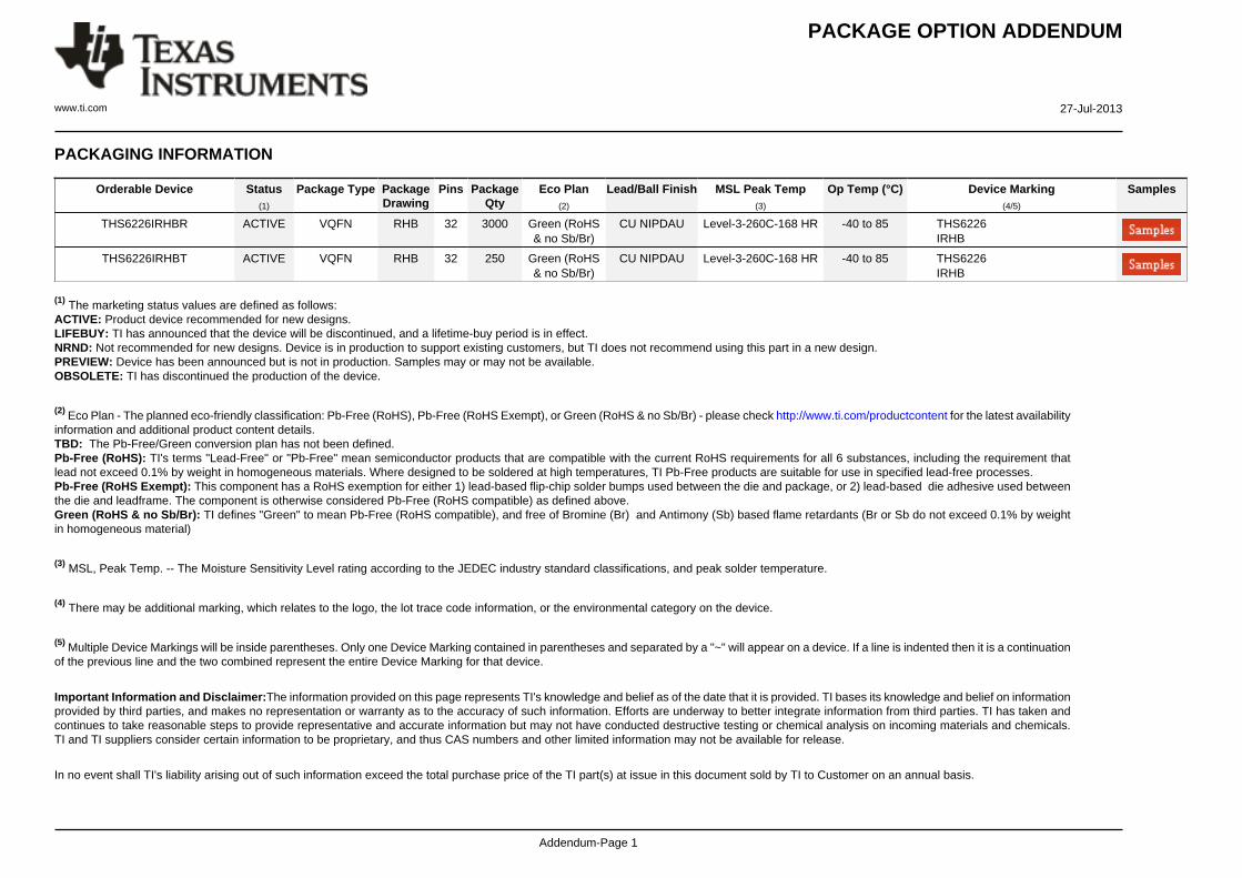
ORDERING INFORMATION (1)
PACKAGEPRODUCT (2) PACKAGE-LEAD DESIGNATOR PACKAGE MARKING TRANSPORT MEDIA, QUANTITY
THS6226IRHBT Tape and Reel, 250VQFN-32 RHB THS6226IRHB
THS6226IRHBR Tape and Reel, 3000
(1) For the most current package and ordering information, see the Package Option Addendum at the end of this document, or visit thedevice product folder at www.ti.com.
(2) The PowerPAD is electrically isolated from all other pins.
ABSOLUTE MAXIMUM RATINGS (1)
Over operating free-air temperature range, unless otherwise noted.
PARAMETER THS6226 UNIT
Supply voltage, GND to VS+, class AB only 15 V
Supply voltage, GND to VS+, class H only 12.5 V
Input voltage, VI 15 V
Output current, IO: static dc (2) ±100 mA
Continuous power dissipation See Thermal Information table
Normal storage temperature –40 to +85 °CMaximum junction temperature, any condition, TJ
(3) +150 °CMaximum junction temperature, continuous operation, long-term reliability, TJ
(4) +130 °CStorage temperature range, TSTG –65 to +150 °C
Human body model (HBM) 2000 VESD Charged device model (CDM) 500 Vratings:
Machine model (MM) 100 V
(1) Stresses above those listed under absolute maximum ratings may cause permanent damage to the device. These are stress ratingsonly, and functional operation of the device at these or any other conditions beyond those indicated under recommended operatingconditions is not implied. Exposure to absolute maximum rated conditions for extended periods may degrade device reliability.
(2) The THS6226 incorporates a PowerPAD on the underside of the chip. This acts as a heatsink and must be connected to a thermallydissipating plane for proper power dissipation. Failure to do so may result in exceeding the maximum junction temperature which couldpermanently damage the device. See TI Technical Brief SLMA002 for more information about utilizing the PowerPADthermally-enhanced package. Under high-frequency ac operation (> 10kHz), the short-term output current capability is much greaterthan the continuous dc output current rating. This short-term output current rating is about 8.5x the dc capability, or approximately±850mA.
(3) The absolute maximum junction temperature under any condition is limited by the constraints of the silicon process.(4) The absolute maximum junction temperature for continuous operation is limited by the package constraints. Operation above this
temperature may result in reduced reliability and/or lifetime of the device.
THERMAL INFORMATIONTHS6226
THERMAL METRIC (1) RHB UNITS
32 PINS
θJA Junction-to-ambient thermal resistance 35.1
θJCtop Junction-to-case (top) thermal resistance 22.1
θJB Junction-to-board thermal resistance 7.0°C/W
ψJT Junction-to-top characterization parameter 0.3
ψJB Junction-to-board characterization parameter 6.9
θJCbot Junction-to-case (bottom) thermal resistance 1.3
(1) For more information about traditional and new thermal metrics, see the IC Package Thermal Metrics application report, SPRA953.
2 Submit Documentation Feedback Copyright © 2011, Texas Instruments Incorporated
Product Folder Link(s): THS6226
THS6226
www.ti.com SBOS499C –JANUARY 2011–REVISED APRIL 2011
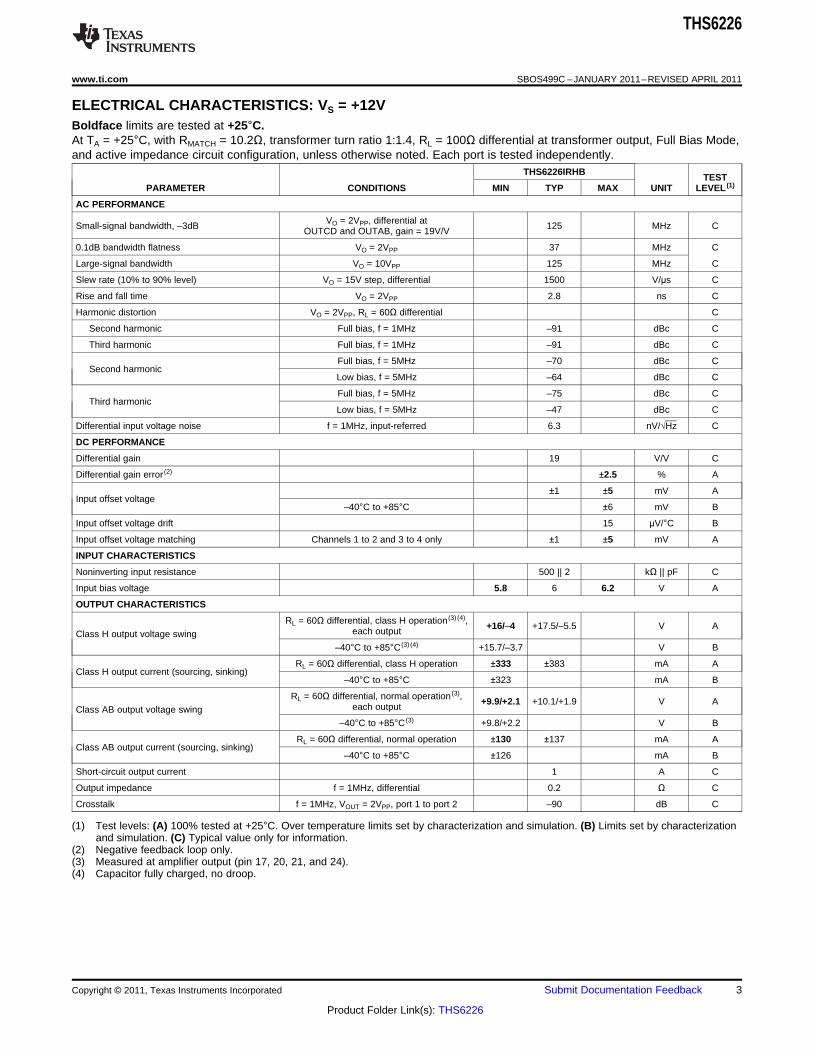
ELECTRICAL CHARACTERISTICS: VS = +12VBoldface limits are tested at +25°C.At TA = +25°C, with RMATCH = 10.2Ω, transformer turn ratio 1:1.4, RL = 100Ω differential at transformer output, Full Bias Mode,and active impedance circuit configuration, unless otherwise noted. Each port is tested independently.
THS6226IRHBTEST
PARAMETER CONDITIONS MIN TYP MAX UNIT LEVEL (1)
AC PERFORMANCE
VO = 2VPP, differential atSmall-signal bandwidth, –3dB 125 MHz COUTCD and OUTAB, gain = 19V/V
0.1dB bandwidth flatness VO = 2VPP 37 MHz C
Large-signal bandwidth VO = 10VPP 125 MHz C
Slew rate (10% to 90% level) VO = 15V step, differential 1500 V/μs C
Rise and fall time VO = 2VPP 2.8 ns C
Harmonic distortion VO = 2VPP, RL = 60Ω differential C
Second harmonic Full bias, f = 1MHz –91 dBc C
Third harmonic Full bias, f = 1MHz –91 dBc C
Full bias, f = 5MHz –70 dBc CSecond harmonic
Low bias, f = 5MHz –64 dBc C
Full bias, f = 5MHz –75 dBc CThird harmonic
Low bias, f = 5MHz –47 dBc C
Differential input voltage noise f = 1MHz, input-referred 6.3 nV/√Hz C
DC PERFORMANCE
Differential gain 19 V/V C
Differential gain error (2) ±2.5 % A
±1 ±5 mV AInput offset voltage
–40°C to +85°C ±6 mV B
Input offset voltage drift 15 μV/°C B
Input offset voltage matching Channels 1 to 2 and 3 to 4 only ±1 ±5 mV A
INPUT CHARACTERISTICS
Noninverting input resistance 500 || 2 kΩ || pF C
Input bias voltage 5.8 6 6.2 V A
OUTPUT CHARACTERISTICS
RL = 60Ω differential, class H operation (3) (4), +16/–4 +17.5/–5.5 V Aeach outputClass H output voltage swing–40°C to +85°C (3) (4) +15.7/–3.7 V B
RL = 60Ω differential, class H operation ±333 ±383 mA AClass H output current (sourcing, sinking)
–40°C to +85°C ±323 mA B
RL = 60Ω differential, normal operation (3), +9.9/+2.1 +10.1/+1.9 V Aeach outputClass AB output voltage swing–40°C to +85°C (3) +9.8/+2.2 V B
RL = 60Ω differential, normal operation ±130 ±137 mA AClass AB output current (sourcing, sinking)
–40°C to +85°C ±126 mA B
Short-circuit output current 1 A C
Output impedance f = 1MHz, differential 0.2 Ω C
Crosstalk f = 1MHz, VOUT = 2VPP, port 1 to port 2 –90 dB C
(1) Test levels: (A) 100% tested at +25°C. Over temperature limits set by characterization and simulation. (B) Limits set by characterizationand simulation. (C) Typical value only for information.
(2) Negative feedback loop only.(3) Measured at amplifier output (pin 17, 20, 21, and 24).(4) Capacitor fully charged, no droop.
Copyright © 2011, Texas Instruments Incorporated Submit Documentation Feedback 3
Product Folder Link(s): THS6226
THS6226
SBOS499C –JANUARY 2011–REVISED APRIL 2011 www.ti.com
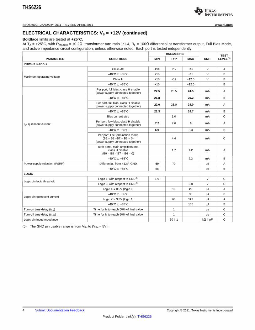
ELECTRICAL CHARACTERISTICS: VS = +12V (continued)Boldface limits are tested at +25°C.At TA = +25°C, with RMATCH = 10.2Ω, transformer turn ratio 1:1.4, RL = 100Ω differential at transformer output, Full Bias Mode,and active impedance circuit configuration, unless otherwise noted. Each port is tested independently.
THS6226IRHBTEST
PARAMETER CONDITIONS MIN TYP MAX UNIT LEVEL (1)
POWER SUPPLY
Class AB +10 +12 +15 V A
–40°C to +85°C +10 +15 V BMaximum operating voltage
Class H +10 +12 +12.5 V B
–40°C to +85°C +10 +12.5 B
Per port, full bias, class H enable 22.5 23.5 24.5 mA A(power supply connected together)
–40°C to +85°C 21.8 25.2 mA B
Per port, full bias, class H disable 22.0 23.0 24.0 mA A(power supply connected together)
–40°C to +85°C 21.3 24.7 mA B
Bias current step 1.0 mA C
Per port, low bias, class H disable 7.2 7.6 8 mA AIS+ quiescent current (power supply connected together)
–40°C to +85°C 6.9 8.3 mA B
Per port, line termination mode(B9 = B8 =B7 = B6 = 0) 4.4 mA C
(power supply connected together)
Both ports, main amplifiers andclass H disable 1.7 2.2 mA A
(B9 = B8 = B7 = B6 = 0)
–40°C to +85°C 2.3 mA B
Power-supply rejection (PSRR) Differential, from +12V, GND 60 70 dB A
–40°C to +85°C 58 dB B
LOGIC
Logic 1, with respect to GND (5) 1.9 V CLogic pin logic threshold
Logic 0, with respect to GND (5) 0.8 V C
Logic X = 0.5V (logic 0) 10 25 μA A
–40°C to +85°C 30 μA BLogic pin quiescent current
Logic X = 3.3V (logic 1) 66 125 μA A
–40°C to +85°C 130 μA B
Turn-on time delay (tON) Time for IS to reach 50% of final value 1 μs C
Turn-off time delay (tOFF) Time for IS to reach 50% of final value 1 μs C
Logic pin input impedance 50 || 1 kΩ || pF C
(5) The GND pin usable range is from VS– to (VS+ – 5V).
4 Submit Documentation Feedback Copyright © 2011, Texas Instruments Incorporated
Product Folder Link(s): THS6226

1
2
3
4
5
6
7
8
24
23
22
21
20
19
18
17
32
9
31
10
30
11
29
12
28
13
27
14
26
15
25
16
GND
INA
INB
CLK
DATA
INC
IND
GND
VA
BH
_E
N
VLL_A
B
CA
PL_A
B
GN
D
VA
BS
VA
BS
CA
PH
_A
B
VH
H_A
B
OUTA
FB_A
FB_B
OUTB
OUTC
FB_C
FB_D
OUTD
VC
DH
_E
N
VLL_C
D
CA
PL_C
D
GN
D
VC
DS
VC
DS
CA
PH
_C
D
VH
H_C
D
THS6226
www.ti.com SBOS499C –JANUARY 2011–REVISED APRIL 2011
PIN CONFIGURATIONS
QFN-32(1)(2)
RHB PACKAGE(TOP VIEW)
(1) The PowerPAD is electrically isolated from all other pins and can be connected to any potential voltage range fromVS– to VS+. Typically, the PowerPAD is connected to the GND plane because this plane tends to physically be thelargest and is able to dissipate the most amount of heat.
(2) The THS6226 defaults to the disabled mode at power-up.
Copyright © 2011, Texas Instruments Incorporated Submit Documentation Feedback 5
Product Folder Link(s): THS6226

CLK
DATA
2 4 6 81 3 5 7 9 10 11 12
tSETUP
tHOLD
tCL
THS6226
SBOS499C –JANUARY 2011–REVISED APRIL 2011 www.ti.com
PIN DESCRIPTIONSNAME PIN DESCRIPTION
GND 1 Analog ground
IND 2 Input D of amplifier CD
INC 3 Input C of amplifier CD
DATA 4 Serial interface data pin
CLK 5 Serial interface CLK pin
INB 6 Input B of amplifier AB
INA 7 Input A of amplifier AB
GND 8 Analog ground
VH_ENAB 9 Class H mode control pin for amplifier AB
VLL_AB 10 Amplifier AB low pump supply
CAPL_AB 11 Amplifier AB negative voltage pump capacitor pin
GND 12 Analog ground
VSAB 13 Amplifier AB supply voltage
VSAB 14 Amplifier AB supply voltage
CAPH_AB 15 Amplifier AB positive voltage pump capacitor pin
VHH_AB 16 Amplifier AB high pump supply
OUTA 17 Output A of amplifier AB
FB_A 18 Feedback for active output impedance of amplifier AB
FB_B 19 Feedback for active output impedance of amplifier AB
OUTB 20 Output B of amplifier AB
OUTC 21 Output C of amplifier CD
FB_C 22 Feedback for active output impedance of amplifier CD
FB_D 23 Feedback for active output impedance of amplifier CD
OUTD 24 Output D of amplifier CD
VHH_CD 25 Amplifier CD high pump supply
CAPH_CD 26 Amplifier CD positive voltage pump capacitor pin
VSCD 27 Amplifier CD supply voltage
VSCD 28 Amplifier CD supply voltage
GND 29 Analog ground
CAPL_CD 30 Amplifier CD negative voltage pump capacitor pin
VLL_CD 31 Amplifier CD low pump supply
VH_ENCD 32 Class H mode control pin for amplifier CD
TIMING CHARACTERISTICS
Figure 1. Serial Interface Timing
THS6226
PARAMETER DESCRIPTION MIN MAX UNITS
tSETUP Setup time 3 ns
tHOLD Hold time 0.5 ns
tCL Clock period 200 ns
6 Submit Documentation Feedback Copyright © 2011, Texas Instruments Incorporated
Product Folder Link(s): THS6226

−21
−18
−15
−12
−9
−6
−3
0
3
1 10 100 300Frequency ( MHz)
Nor
mal
ized
Gai
n (d
B)
Bias 15Bias 10Bias 5Bias 0
VO = 2VPPRL = 60Ω
−21
−18
−15
−12
−9
−6
−3
0
3
1 10 100 300Frequency ( MHz)
Nor
mal
ized
Gai
n (d
B)
Bias 15Bias 10Bias 5Bias 0
VO = 10VPPRL = 60Ω
-12.5 -9.5 -6.5 -3.5 -0.5 20.5100
400
450
500
550
600
650
Output Power (dBm)
Pow
er
Consum
ption (
mW
)
2.5 5.5
Prof. 30, Bias 10
Prof. 17, Bias 4
Prof. 8, Bias 2
ADSL, Bias 0
350
300
250
200
150
8.5 11.5 14.5 17.5
Output Power Into 100 Load
Load Power Included
W
-350 -250 -150 -50 50 3500
2
4
6
8
10
12
I (mA)O
V(V
)O
1W Internal
Power
Dissipation
Bias 15
Class AB Mode
1W Internal
Power
Dissipation
150 250
100 Load LineW
50 Load LineW
25 Load LineW
0 20 40 60 80 100 120 140 160 180 2000.27
0.21
0.16
0.11
0.05
0
0.05
0.11
0.16
0.21
0.27
-5
-4
-3
-2
-1
0
1
2
3
4
5
Time (ns)
Input V
oltage (
V)
Outp
ut V
oltage (
V)
R = 60WL
AC-Coupled Input and Output
Output Voltage
Right Scale
Input Voltage
Left Scale
0.6 0.7 0.8 0.9 1 1.1 1.2 1.3 1.4 1.5 1.6-0.21
-0.11
0
0.11
0.21
0.32
0.43
0.53
0.64
0.75
-4
-2
0
2
4
6
8
10
12
14
Time (ns)
Input V
oltage (
V)
Outp
ut V
oltage (
V)
Input Voltage
Left Scale
Output Voltage
Right Scale
R = 60WL
AC-Coupled
Input and Output
Positive Excursion Only
THS6226
www.ti.com SBOS499C –JANUARY 2011–REVISED APRIL 2011
TYPICAL CHARACTERISTICS: VS = +12VAt TA = +25°C and Full Bias Mode, unless otherwise noted
SMALL-SIGNAL FREQUENCY RESPONSE LARGE-SIGNAL FREQUENCY RESPONSE
Figure 2. Figure 3.
OUTPUT VOLTAGE AND CURRENT LIMITATIONS POWER CONSUMPTION
Figure 4. Figure 5.
CLASS AB OVERDRIVE RECOVERY OVERDRIVE RECOVERY
Figure 6. Figure 7.
Copyright © 2011, Texas Instruments Incorporated Submit Documentation Feedback 7
Product Folder Link(s): THS6226

1
10
100
100 1k 10k 100k 1M
Frequency (Hz)
Inp
ut
Vo
lta
ge
No
ise
De
nsity (
nV
/)
ÖH
z
−100
−95
−90
−85
−80
−75
−70
−65
−60
−55
−50
0.5 1 10 30Frequency (MHz)
Har
mon
ic D
isto
rtio
n (d
Bc)
2nd Harmonic3rd Harmonic
VO = 2VPPRL = 100Ω1:1.4 Transformer
−85
−80
−75
−70
−65
−60
50 60 70 80 90 100 110 120 130 140 150
Load (Ω)
Har
mon
ic D
isto
rtio
n (d
Bc)
2nd Harmonic3rd Harmonic
VO = 2VPP
1:1.4 Transformerf = 5MHz
105
100
95
90
85
80
75
70
65
60
0 10 15 20 25 30
Frequency (Hz)
3rd
-Ord
er
Inte
rmo
du
latio
n S
pu
rio
us (
dB
c)
2V Envelope
R = 100
1:1.4 Transformer
W
PP
L
5
80
75
70
65
60
55
50
45
40
35
30
0 10 12 14 16 18 20
Output Voltage (V )PP
Ha
rmo
nic
Dis
tort
ion
(d
Bc)
2nd Harmonic
3rd Harmonic
2 4 6 8
f = 5MHz
R = 100
1:1.4 Transformer
WL
−80
−75
−70
−65
−60
−55
−50
−45
−40
0 1 2 3 4 5 6 7 8 9 10 11 12 13 14 15Bias Current Mode
Har
mon
ic D
isto
rtio
n (d
Bc)
2nd Harmonic3rd Harmonic
f = 5MHzVO = 2VPPRL = 100Ω1:1.4 Transformer
THS6226
SBOS499C –JANUARY 2011–REVISED APRIL 2011 www.ti.com
TYPICAL CHARACTERISTICS: VS = +12V (continued)At TA = +25°C and Full Bias Mode, unless otherwise noted
INPUT NOISE DENSITY HARMONIC DISTORTION vs FREQUENCY
Figure 8. Figure 9.
TWO-TONE, THIRD-ORDERHARMONIC DISTORTION vs LOAD INTERMODULATION SPURIOUS
Figure 10. Figure 11.
HARMONIC DISTORTION vs OUTPUT VOLTAGE HARMONIC DISTORTION vs BIAS CURRENT
Figure 12. Figure 13.
8 Submit Documentation Feedback Copyright © 2011, Texas Instruments Incorporated
Product Folder Link(s): THS6226

-5
-4
-3
-2
-1
0
1
2
3
4
5
-5 0 10 15 20 25 30
Time (ns)
Dis
able
Voltage (
V)
5
Disable Disable
Enable
70
60
50
40
30
20
10
0
1M 10M 100M 1G 6G
Frequency (Hz)
Gain
(dB
)
Differential at Amplifier Output
VO = 200mVPP
−50 −25 0 25 50 75 100 12521
21.3
21.6
21.9
22.2
22.5
22.8
23.1
23.4
23.7
24
380
382
384
386
388
390
392
394
396
398
400
Temperature (°C)
Qui
esce
nt C
urre
nt (
mA
)
Out
put C
urre
nt (
mA
)
Quiescent Current (Bias 15)Output Current
−80
−70
−60
−50
−40
−30
−20
−10
0
100k 1M 10M 100MFrequency (Hz)
Pow
er−
Sup
ply
Rej
ectio
n R
atio
Com
mon
−M
ode
Rej
ectio
n R
atio
(dB
)
+PSRRCMRR
0
0.2
0.5
0.8
1
1.2
1.5
1.8
2
−50 −25 0 25 50 75 100 125Temperature (°C)
Inpu
t Offs
et V
olta
ge (
mV
)
350
300
250
200
150
100
50
0
Population (mV)
Co
un
ts
-0
.42
-1
.26
-2
.1
-2
.94
-3
.78
-4
.62
-5
.46
0.4
2
1.2
6
2.1
2.9
4
3.7
8
4.6
2
5.4
6
THS6226
www.ti.com SBOS499C –JANUARY 2011–REVISED APRIL 2011
TYPICAL CHARACTERISTICS: VS = +12V (continued)At TA = +25°C and Full Bias Mode, unless otherwise noted
LARGE-SIGNAL ENABLE/DISABLE RESPONSE DISABLE FEEDTHROUGH vs FREQUENCY
Figure 14. Figure 15.
QUIESCENT CURRENT AND OUTPUTPSRR AND CMRR vs FREQUENCY vs TEMPERATURE
Figure 16. Figure 17.
INPUT OFFSET VOLTAGE vs TEMPERATURE INPUT OFFSET VOLTAGE HISTOGRAM
Figure 18. Figure 19.
Copyright © 2011, Texas Instruments Incorporated Submit Documentation Feedback 9
Product Folder Link(s): THS6226
VIN+
VIN -
+12V
33nF10.2W
THS62261:1.4
100kW
+12V
CLK
DATA
1 Fm
1 Fm
OUTD
OUTC
IND
INC
VLL_CD
VHH_CD
CAPL_CD
CAPH_CD
FBC
FBD
Line:
100W
THS6226
SBOS499C –JANUARY 2011–REVISED APRIL 2011 www.ti.com
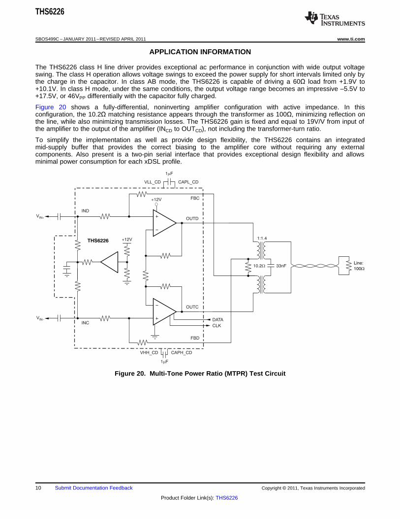
APPLICATION INFORMATION
The THS6226 class H line driver provides exceptional ac performance in conjunction with wide output voltageswing. The class H operation allows voltage swings to exceed the power supply for short intervals limited only bythe charge in the capacitor. In class AB mode, the THS6226 is capable of driving a 60Ω load from +1.9V to+10.1V. In class H mode, under the same conditions, the output voltage range becomes an impressive –5.5V to+17.5V, or 46VPP differentially with the capacitor fully charged.
Figure 20 shows a fully-differential, noninverting amplifier configuration with active impedance. In thisconfiguration, the 10.2Ω matching resistance appears through the transformer as 100Ω, minimizing reflection onthe line, while also minimizing transmission losses. The THS6226 gain is fixed and equal to 19V/V from input ofthe amplifier to the output of the amplifier (INCD to OUTCD), not including the transformer-turn ratio.
To simplify the implementation as well as provide design flexibility, the THS6226 contains an integratedmid-supply buffer that provides the correct biasing to the amplifier core without requiring any externalcomponents. Also present is a two-pin serial interface that provides exceptional design flexibility and allowsminimal power consumption for each xDSL profile.
Figure 20. Multi-Tone Power Ratio (MTPR) Test Circuit
10 Submit Documentation Feedback Copyright © 2011, Texas Instruments Incorporated
Product Folder Link(s): THS6226

DATA B0 B1 B2 B3 B4 B5 B6 B7 B8 B9 B10 B11
Start
Bit
Start
Bit
Ch AB
Select
Ch CD
Select
PD1 PD0 D3 D2 D1 D0 Parity Stop
Bit
MSB LSB
THS6226
www.ti.com SBOS499C –JANUARY 2011–REVISED APRIL 2011
PROGRAMMING THE THS6226
Programming of the THS6226 is realized through a serial interface (pins 4 and 5) and proceeds in the followingsequence.
Two start bits are required B0 = 0 followed by B1 = 1.B2 through B9 are used to program the THS6226.Refer to Table 1 for the bit descriptions.B10 (refer to Table 2) is the parity bit that controls if the word is or is not loaded.B11 is the stop bit and should be set to B11 = 1. Figure 21 shows the sequence to be adopted.
Table 1. SDATA
PARAMETER DESCRIPTION
B0, B1 Start bit
B2, B3 Channel select
B4, B5 Power-down features
B6-B9 Quiescent current setting
B10 Parity bit
B11 Stop bit
Table 2. Parity Bit
B10 ODD PARITY BIT
0 If odd, number of high bits in B2 to B9
1 If even, number of high bits in B2 to B9
Figure 21. DATA Description
Copyright © 2011, Texas Instruments Incorporated Submit Documentation Feedback 11
Product Folder Link(s): THS6226
THS6226
SBOS499C –JANUARY 2011–REVISED APRIL 2011 www.ti.com
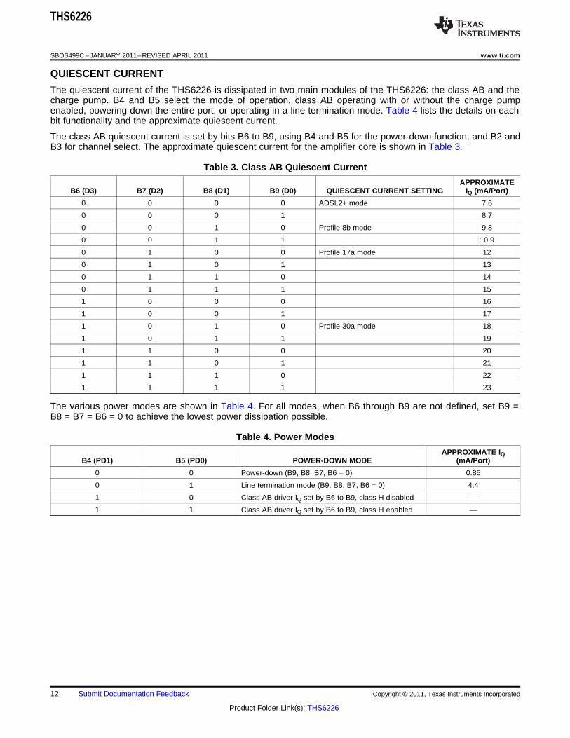
QUIESCENT CURRENT
The quiescent current of the THS6226 is dissipated in two main modules of the THS6226: the class AB and thecharge pump. B4 and B5 select the mode of operation, class AB operating with or without the charge pumpenabled, powering down the entire port, or operating in a line termination mode. Table 4 lists the details on eachbit functionality and the approximate quiescent current.
The class AB quiescent current is set by bits B6 to B9, using B4 and B5 for the power-down function, and B2 andB3 for channel select. The approximate quiescent current for the amplifier core is shown in Table 3.
Table 3. Class AB Quiescent Current
APPROXIMATEB6 (D3) B7 (D2) B8 (D1) B9 (D0) QUIESCENT CURRENT SETTING IQ (mA/Port)
0 0 0 0 ADSL2+ mode 7.6
0 0 0 1 8.7
0 0 1 0 Profile 8b mode 9.8
0 0 1 1 10.9
0 1 0 0 Profile 17a mode 12
0 1 0 1 13
0 1 1 0 14
0 1 1 1 15
1 0 0 0 16
1 0 0 1 17
1 0 1 0 Profile 30a mode 18
1 0 1 1 19
1 1 0 0 20
1 1 0 1 21
1 1 1 0 22
1 1 1 1 23
The various power modes are shown in Table 4. For all modes, when B6 through B9 are not defined, set B9 =B8 = B7 = B6 = 0 to achieve the lowest power dissipation possible.
Table 4. Power Modes
APPROXIMATE IQB4 (PD1) B5 (PD0) POWER-DOWN MODE (mA/Port)
0 0 Power-down (B9, B8, B7, B6 = 0) 0.85
0 1 Line termination mode (B9, B8, B7, B6 = 0) 4.4
1 0 Class AB driver IQ set by B6 to B9, class H disabled —1 1 Class AB driver IQ set by B6 to B9, class H enabled —
12 Submit Documentation Feedback Copyright © 2011, Texas Instruments Incorporated
Product Folder Link(s): THS6226

THS6226
www.ti.com SBOS499C –JANUARY 2011–REVISED APRIL 2011
Channel selection is shown in Table 5. Each channel can be programmed independently, or together if both B2and B3 are set to '1'.
Table 5. Channel Selection
B2 (Channel AB) B3 (Channel CD) CHANNEL SELECT
0 0 Bits B4 to B9 are ignored
0 1 Channel B programmed with B4 to B9
1 0 Channel A programmed with B4 to B9
1 1 Channels A and B programmed with B4 to B9
At startup, the internal register is set as shown in Table 6.
Table 6. Internal Register
B2 B3(Channel AB) (Channel CD) B4 (PD1) B5 (PD0) B6 (D3) B7 (D2) B8 (D1) B9 (D0)
0 0 0 0 0 0 0 0
In this condition, the total quiescent power dissipation is 10.2mW/port on a +12V supply.
Copyright © 2011, Texas Instruments Incorporated Submit Documentation Feedback 13
Product Folder Link(s): THS6226

THS6226
SBOS499C –JANUARY 2011–REVISED APRIL 2011 www.ti.com
REVISION HISTORY
NOTE: Page numbers for previous revisions may differ from page numbers in the current version.
Changes from Revision B (February 2011) to Revision C Page
• Changed LOGIC, Logic pin input impedance typical specification and unit in Electrical Characteristics table .................... 4
• Changed Timing Characteristics section .............................................................................................................................. 6
14 Submit Documentation Feedback Copyright © 2011, Texas Instruments Incorporated
Product Folder Link(s): THS6226
PACKAGE OPTION ADDENDUM
www.ti.com 27-Jul-2013
Addendum-Page 1
PACKAGING INFORMATION
Orderable Device Status(1)
Package Type PackageDrawing
Pins PackageQty
Eco Plan(2)
Lead/Ball Finish MSL Peak Temp(3)
Op Temp (°C) Device Marking(4/5)
Samples
THS6226IRHBR ACTIVE VQFN RHB 32 3000 Green (RoHS& no Sb/Br)
CU NIPDAU Level-3-260C-168 HR -40 to 85 THS6226IRHB
THS6226IRHBT ACTIVE VQFN RHB 32 250 Green (RoHS& no Sb/Br)
CU NIPDAU Level-3-260C-168 HR -40 to 85 THS6226IRHB
(1) The marketing status values are defined as follows:ACTIVE: Product device recommended for new designs.LIFEBUY: TI has announced that the device will be discontinued, and a lifetime-buy period is in effect.NRND: Not recommended for new designs. Device is in production to support existing customers, but TI does not recommend using this part in a new design.PREVIEW: Device has been announced but is not in production. Samples may or may not be available.OBSOLETE: TI has discontinued the production of the device.
(2) Eco Plan - The planned eco-friendly classification: Pb-Free (RoHS), Pb-Free (RoHS Exempt), or Green (RoHS & no Sb/Br) - please check http://www.ti.com/productcontent for the latest availabilityinformation and additional product content details.TBD: The Pb-Free/Green conversion plan has not been defined.Pb-Free (RoHS): TI's terms "Lead-Free" or "Pb-Free" mean semiconductor products that are compatible with the current RoHS requirements for all 6 substances, including the requirement thatlead not exceed 0.1% by weight in homogeneous materials. Where designed to be soldered at high temperatures, TI Pb-Free products are suitable for use in specified lead-free processes.Pb-Free (RoHS Exempt): This component has a RoHS exemption for either 1) lead-based flip-chip solder bumps used between the die and package, or 2) lead-based die adhesive used betweenthe die and leadframe. The component is otherwise considered Pb-Free (RoHS compatible) as defined above.Green (RoHS & no Sb/Br): TI defines "Green" to mean Pb-Free (RoHS compatible), and free of Bromine (Br) and Antimony (Sb) based flame retardants (Br or Sb do not exceed 0.1% by weightin homogeneous material)
(3) MSL, Peak Temp. -- The Moisture Sensitivity Level rating according to the JEDEC industry standard classifications, and peak solder temperature.
(4) There may be additional marking, which relates to the logo, the lot trace code information, or the environmental category on the device.
(5) Multiple Device Markings will be inside parentheses. Only one Device Marking contained in parentheses and separated by a "~" will appear on a device. If a line is indented then it is a continuationof the previous line and the two combined represent the entire Device Marking for that device.
Important Information and Disclaimer:The information provided on this page represents TI's knowledge and belief as of the date that it is provided. TI bases its knowledge and belief on informationprovided by third parties, and makes no representation or warranty as to the accuracy of such information. Efforts are underway to better integrate information from third parties. TI has taken andcontinues to take reasonable steps to provide representative and accurate information but may not have conducted destructive testing or chemical analysis on incoming materials and chemicals.TI and TI suppliers consider certain information to be proprietary, and thus CAS numbers and other limited information may not be available for release.
In no event shall TI's liability arising out of such information exceed the total purchase price of the TI part(s) at issue in this document sold by TI to Customer on an annual basis.
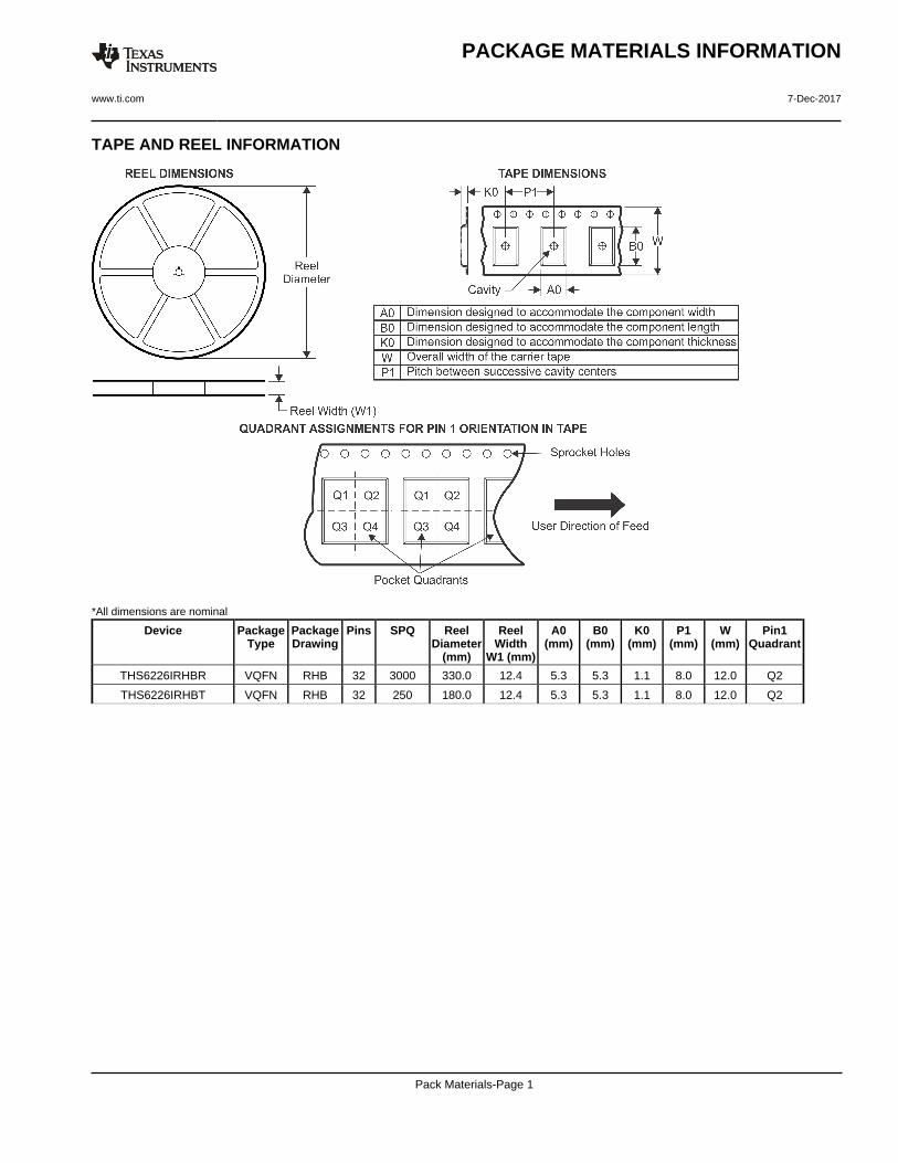
TAPE AND REEL INFORMATION
*All dimensions are nominal
Device PackageType
PackageDrawing
Pins SPQ ReelDiameter
(mm)
ReelWidth
W1 (mm)
A0(mm)
B0(mm)
K0(mm)
P1(mm)
W(mm)
Pin1Quadrant
THS6226IRHBR VQFN RHB 32 3000 330.0 12.4 5.3 5.3 1.1 8.0 12.0 Q2
THS6226IRHBT VQFN RHB 32 250 180.0 12.4 5.3 5.3 1.1 8.0 12.0 Q2
PACKAGE MATERIALS INFORMATION
www.ti.com 7-Dec-2017
Pack Materials-Page 1

*All dimensions are nominal
Device Package Type Package Drawing Pins SPQ Length (mm) Width (mm) Height (mm)
THS6226IRHBR VQFN RHB 32 3000 367.0 367.0 35.0
THS6226IRHBT VQFN RHB 32 250 210.0 185.0 35.0
PACKAGE MATERIALS INFORMATION
www.ti.com 7-Dec-2017
Pack Materials-Page 2

IMPORTANT NOTICE
Texas Instruments Incorporated (TI) reserves the right to make corrections, enhancements, improvements and other changes to itssemiconductor products and services per JESD46, latest issue, and to discontinue any product or service per JESD48, latest issue. Buyersshould obtain the latest relevant information before placing orders and should verify that such information is current and complete.TI’s published terms of sale for semiconductor products (http://www.ti.com/sc/docs/stdterms.htm) apply to the sale of packaged integratedcircuit products that TI has qualified and released to market. Additional terms may apply to the use or sale of other types of TI products andservices.Reproduction of significant portions of TI information in TI data sheets is permissible only if reproduction is without alteration and isaccompanied by all associated warranties, conditions, limitations, and notices. TI is not responsible or liable for such reproduceddocumentation. Information of third parties may be subject to additional restrictions. Resale of TI products or services with statementsdifferent from or beyond the parameters stated by TI for that product or service voids all express and any implied warranties for theassociated TI product or service and is an unfair and deceptive business practice. TI is not responsible or liable for any such statements.Buyers and others who are developing systems that incorporate TI products (collectively, “Designers”) understand and agree that Designersremain responsible for using their independent analysis, evaluation and judgment in designing their applications and that Designers havefull and exclusive responsibility to assure the safety of Designers' applications and compliance of their applications (and of all TI productsused in or for Designers’ applications) with all applicable regulations, laws and other applicable requirements. Designer represents that, withrespect to their applications, Designer has all the necessary expertise to create and implement safeguards that (1) anticipate dangerousconsequences of failures, (2) monitor failures and their consequences, and (3) lessen the likelihood of failures that might cause harm andtake appropriate actions. Designer agrees that prior to using or distributing any applications that include TI products, Designer willthoroughly test such applications and the functionality of such TI products as used in such applications.TI’s provision of technical, application or other design advice, quality characterization, reliability data or other services or information,including, but not limited to, reference designs and materials relating to evaluation modules, (collectively, “TI Resources”) are intended toassist designers who are developing applications that incorporate TI products; by downloading, accessing or using TI Resources in anyway, Designer (individually or, if Designer is acting on behalf of a company, Designer’s company) agrees to use any particular TI Resourcesolely for this purpose and subject to the terms of this Notice.TI’s provision of TI Resources does not expand or otherwise alter TI’s applicable published warranties or warranty disclaimers for TIproducts, and no additional obligations or liabilities arise from TI providing such TI Resources. TI reserves the right to make corrections,enhancements, improvements and other changes to its TI Resources. TI has not conducted any testing other than that specificallydescribed in the published documentation for a particular TI Resource.Designer is authorized to use, copy and modify any individual TI Resource only in connection with the development of applications thatinclude the TI product(s) identified in such TI Resource. NO OTHER LICENSE, EXPRESS OR IMPLIED, BY ESTOPPEL OR OTHERWISETO ANY OTHER TI INTELLECTUAL PROPERTY RIGHT, AND NO LICENSE TO ANY TECHNOLOGY OR INTELLECTUAL PROPERTYRIGHT OF TI OR ANY THIRD PARTY IS GRANTED HEREIN, including but not limited to any patent right, copyright, mask work right, orother intellectual property right relating to any combination, machine, or process in which TI products or services are used. Informationregarding or referencing third-party products or services does not constitute a license to use such products or services, or a warranty orendorsement thereof. Use of TI Resources may require a license from a third party under the patents or other intellectual property of thethird party, or a license from TI under the patents or other intellectual property of TI.TI RESOURCES ARE PROVIDED “AS IS” AND WITH ALL FAULTS. TI DISCLAIMS ALL OTHER WARRANTIES ORREPRESENTATIONS, EXPRESS OR IMPLIED, REGARDING RESOURCES OR USE THEREOF, INCLUDING BUT NOT LIMITED TOACCURACY OR COMPLETENESS, TITLE, ANY EPIDEMIC FAILURE WARRANTY AND ANY IMPLIED WARRANTIES OFMERCHANTABILITY, FITNESS FOR A PARTICULAR PURPOSE, AND NON-INFRINGEMENT OF ANY THIRD PARTY INTELLECTUALPROPERTY RIGHTS. TI SHALL NOT BE LIABLE FOR AND SHALL NOT DEFEND OR INDEMNIFY DESIGNER AGAINST ANY CLAIM,INCLUDING BUT NOT LIMITED TO ANY INFRINGEMENT CLAIM THAT RELATES TO OR IS BASED ON ANY COMBINATION OFPRODUCTS EVEN IF DESCRIBED IN TI RESOURCES OR OTHERWISE. IN NO EVENT SHALL TI BE LIABLE FOR ANY ACTUAL,DIRECT, SPECIAL, COLLATERAL, INDIRECT, PUNITIVE, INCIDENTAL, CONSEQUENTIAL OR EXEMPLARY DAMAGES INCONNECTION WITH OR ARISING OUT OF TI RESOURCES OR USE THEREOF, AND REGARDLESS OF WHETHER TI HAS BEENADVISED OF THE POSSIBILITY OF SUCH DAMAGES.Unless TI has explicitly designated an individual product as meeting the requirements of a particular industry standard (e.g., ISO/TS 16949and ISO 26262), TI is not responsible for any failure to meet such industry standard requirements.Where TI specifically promotes products as facilitating functional safety or as compliant with industry functional safety standards, suchproducts are intended to help enable customers to design and create their own applications that meet applicable functional safety standardsand requirements. Using products in an application does not by itself establish any safety features in the application. Designers mustensure compliance with safety-related requirements and standards applicable to their applications. Designer may not use any TI products inlife-critical medical equipment unless authorized officers of the parties have executed a special contract specifically governing such use.Life-critical medical equipment is medical equipment where failure of such equipment would cause serious bodily injury or death (e.g., lifesupport, pacemakers, defibrillators, heart pumps, neurostimulators, and implantables). Such equipment includes, without limitation, allmedical devices identified by the U.S. Food and Drug Administration as Class III devices and equivalent classifications outside the U.S.TI may expressly designate certain products as completing a particular qualification (e.g., Q100, Military Grade, or Enhanced Product).Designers agree that it has the necessary expertise to select the product with the appropriate qualification designation for their applicationsand that proper product selection is at Designers’ own risk. Designers are solely responsible for compliance with all legal and regulatoryrequirements in connection with such selection.Designer will fully indemnify TI and its representatives against any damages, costs, losses, and/or liabilities arising out of Designer’s non-compliance with the terms and provisions of this Notice.
Mailing Address: Texas Instruments, Post Office Box 655303, Dallas, Texas 75265Copyright © 2017, Texas Instruments Incorporated