Embed Size (px)
Citation preview
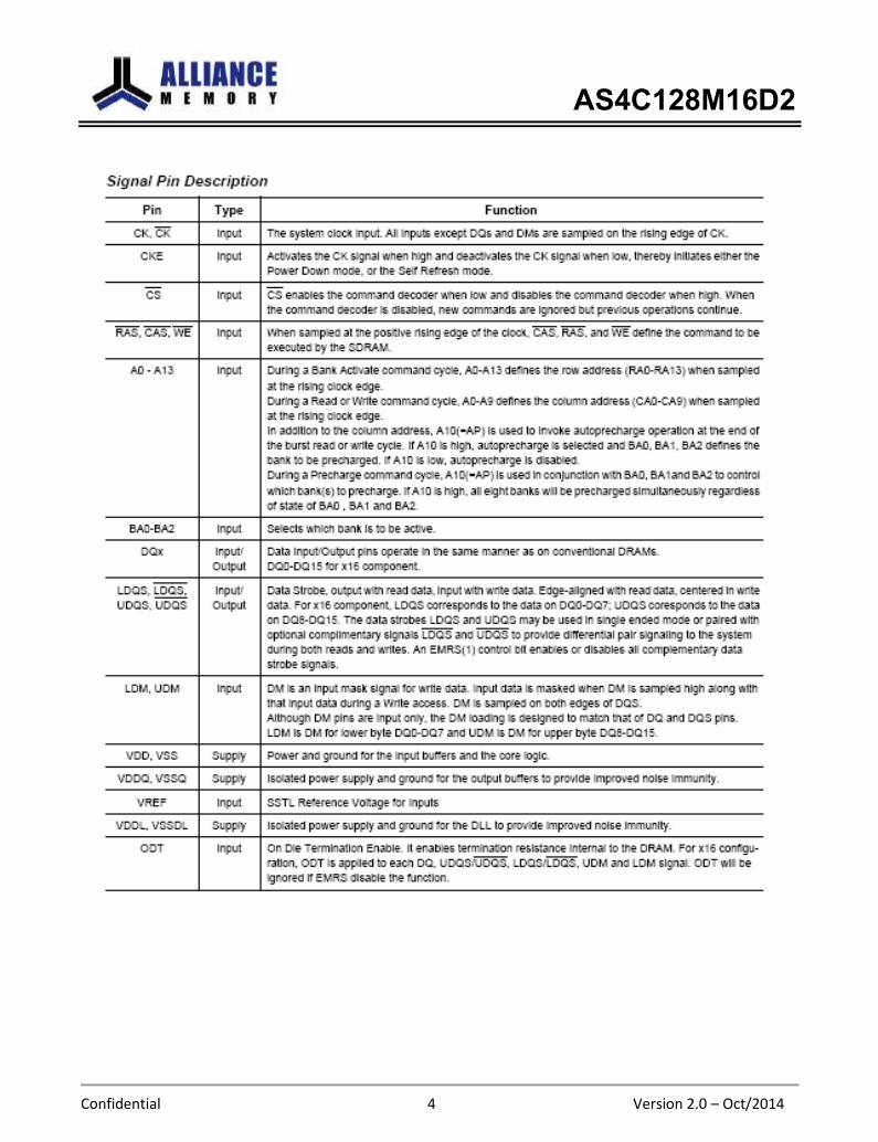
AS4C128M16D2
Revision History AS4C128M16D2- 84-ball FBGA PACKAGE
Revision Details Date
Rev 1.0 Preliminary datasheet March 2014
Rev 2.0 Amended page 74 corrected package dimensions "F" to be " E " and "SF" to be " SE
October 2014
Alliance Memory Inc. 551 Taylor Way, San Carlos, CA 94070 TEL: (650) 610-6800 FAX: (650) 620-9211
Alliance Memory Inc. reserves the right to change products or specification without notice.
Confidential 0 Version 2.0 – October/2014
AS4C128M16D2
Confidential 1 Version 2.0 – October/2014
128M x 16 bit DDRII Synchronous DRAM (SDRAM) Confidential Advanced (Rev. 2.0, October. /2014)
Features
- High speed data transfer rates with system frequency up
to 400 MHz
- 8 internal banks for concurrent operation
- 4-bit prefetch architecture
- Programmable CAS Latency: 3, 4 ,5 , 6 and 7
- Programmable Additive Latency: 0, 1, 2, 3 , 4, 5 and 6
- Write Latency = Read Latency -1
- Programmable Wrap Sequence: Sequential or
Interleave
- Programmable Burst Length: 4 and 8
- Automatic and Controlled Precharge Command
- Power Down Mode
- Auto Refresh and Self Refresh
- Refresh Interval: 7.8 us (8192 cycles/64 ms) Tcase
between 0°C and 85°C
- ODT (On-Die Termination)
- Weak Strength Data-Output Driver Option
- Bidirectional differential Data Strobe (Single-ended
data-strobe is an optional feature)
- On-Chip DLL aligns DQ and DQs transitions with CK
transitions
- DQS can be disabled for single-ended data strobe
- Differential clock inputs CK and CK
- JEDEC Power Supply 1.8V ± 0.1V
- VDDQ =1.8V ± 0.1V
- Available in 84-ball FBGA
- RoHS compliant
- PASR Partial Array Self Refresh
- tRAS lockout supported
Description
The AS4C128M16D2 is an eight bank DDR DRAM organized
as 8 banks x 16Mbit x 16. The AS4C128M16D2 achieves high
speed data transfer rates by employing a chip architecture
that prefetches multiple bits and then synchronizes the
output data to a system clock.
The chip is designed to comply with the following key
DDR2 SDRAM features:(1) posted CAS with additive latency,
(2) write latency = read latency-1, (3) On Die Termination.
All of the control, address, circuits are synchronized
with the positive edge of an externally supplied clock. I/O s
are synchronized with a pair of bidirectional strobes
(DQS, DQS) in a source synchronous fashion.
Operating the eight memory banks in an interleaved
fashion allows random access operation to occur at a
higher rate than is possible with standard DRAMs. A
sequential and gapless data rate is possible depending on
burst length, CAS latency and speed grade of the device.
Table 1. Ordering Information
Part Number Clock Frequency Data Rate Power Supply Package
AS4C128M16D2-25BCN 400MHz 800Mbps/pin VDD 1.8V, VDDQ 1.8V 84 ball FBGA
AS4C128M16D2-25BIN 400MHz 800Mbps/pin VDD 1.8V, VDDQ 1.8V 84 ball FBGA
B: indicates 60-ball 8 x 10 x 1.2mm (max) FBGA package
C: indicates commercial temperature I: indicates industrial temperature
N: indicates Pb and Halogen Free ROHS
Table 2. Speed Grade Information
Speed Grade Clock Frequency CAS Latency tRCD (ns) tRP (ns)
DDR2-800 400 MHz 5 5 5
AS4C128M16D2
Confidential 2 Version 2.0 – Oct/2014
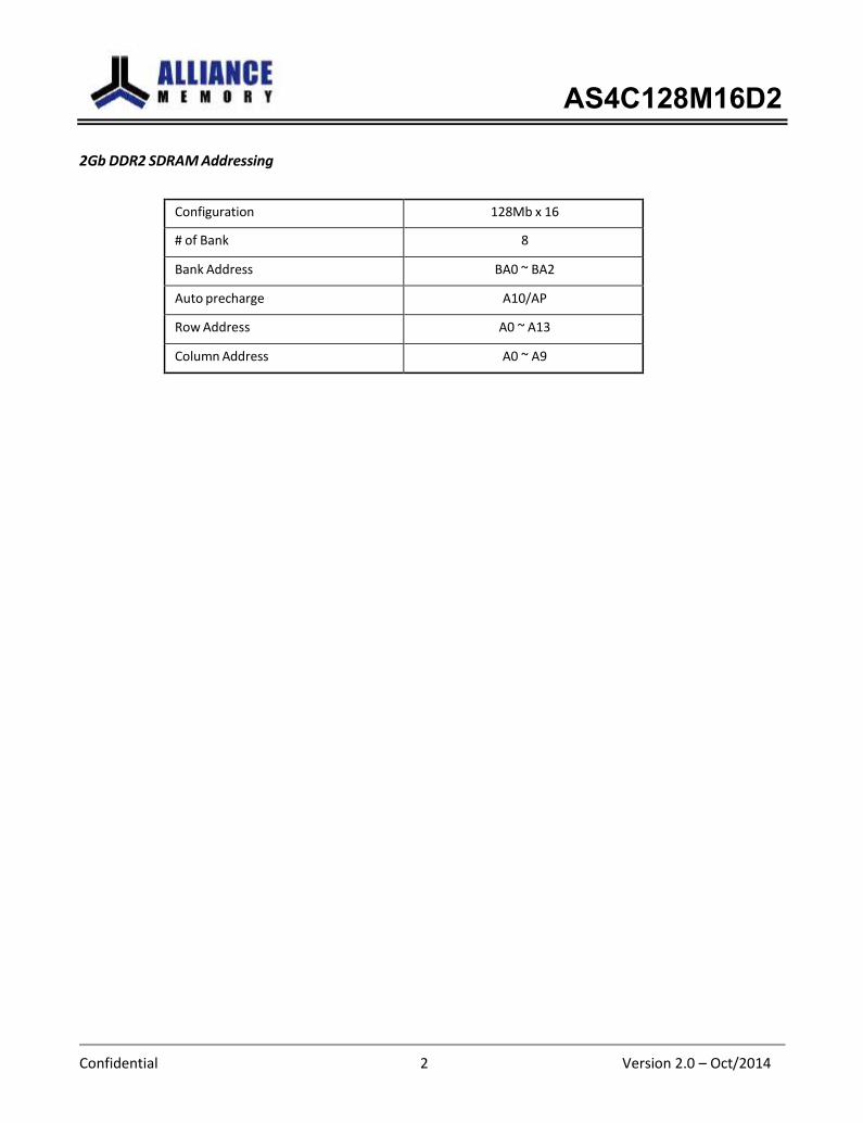
2Gb DDR2 SDRAM Addressing
Configuration 128Mb x 16
# of Bank 8
Bank Address BA0 ~ BA2
Auto precharge A10/AP
Row Address A0 ~ A13
Column Address A0 ~ A9
AS4C128M16D2
Confidential 3 Version 2.0 – October/2014
AS4C128M16D2
Confidential 4 Version 2.0 – Oct/2014
AS4C128M16D2
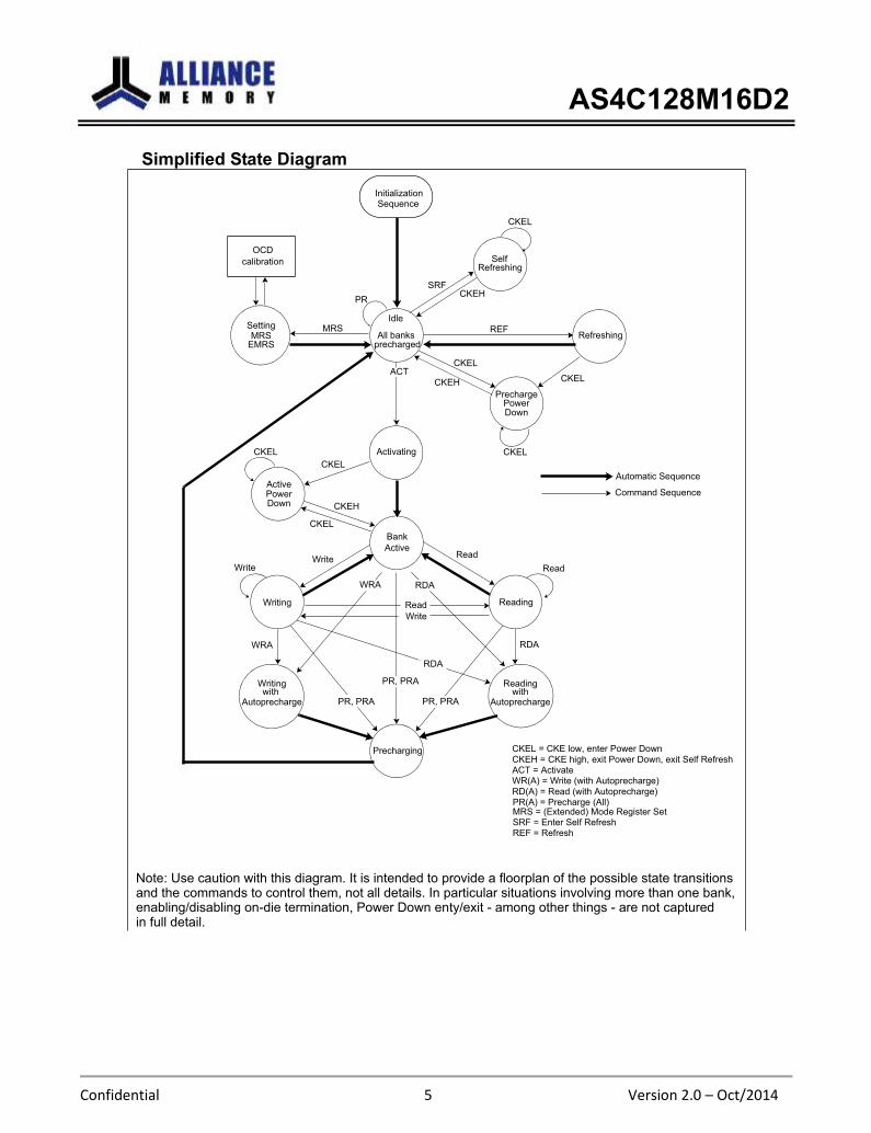
Confidential 5 Version 2.0 – Oct/2014
Self
IdleSetting
EMRS
Bank
Precharging
Power
Writing
ACT
RDA
Read
SRF
REF
CKEL
MRS
CKEH
CKEH
CKEL
Write
Automatic Sequence
Command Sequence
RDAWRA
Read
PR, PRA
PR
Refreshing
Refreshing
Down
PowerDown
Active
with
RDA
Readingwith
WRA
Active
Precharge
ReadingWriting
PR(A) = Precharge (All)MRS = (Extended) Mode Register SetSRF = Enter Self RefreshREF = Refresh
CKEL = CKE low, enter Power DownCKEH = CKE high, exit Power Down, exit Self RefreshACT = ActivateWR(A) = Write (with Autoprecharge)RD(A) = Read (with Autoprecharge)
Note: Use caution with this diagram. It is intended to provide a floorplan of the possible state transitions
Simplified State Diagram
All banksprecharged
Activating
CKEH
ReadWrite
CKEL
MRS
CKEL
SequenceInitialization
OCD
calibration
CKEL
CKEL CKEL
AutoprechargeAutoprecharge PR, PRA PR, PRA
and the commands to control them, not all details. In particular situations involving more than one bank,enabling/disabling on-die termination, Power Down enty/exit - among other things - are not capturedin full detail.
Write

AS4C128M16D2
Confidential 6 Version 2.0 – Oct/2014
Basic Functionality Read and write accesses to the DDR2 SDRAM are burst oriented; accesses start at a selected location and continue for a burst
length of four or eight in a programmed sequence. Accesses begin with the registration of an Active command, which is then
followed by a Read or Write command. The address bits registered coincident with the active command are used to select the
bank and row to be accessed (BA0, BA1 select the bank; A0-A13 select the row). The address bits registered coincident with the
Read or Write command are used to select the starting column location for the burst access and to determine if the auto
precharge command is to be issued.
Prior to normal operation, the DDR2 SDRAM must be initialized. The following sections provide detailed information covering device
initialization, register definition, command descriptions and device operation.
Power up and Initialization DDR2 SDRAMs must be powered up and initialized in a predefined manner. Operational procedures other than those specified may
result in undefined operation.
Power-up and Initialization Sequence
The following sequence is required for POWER UP and Initialization.
1. Apply power and attempt to maintain CKE below 0.2*VDDQ and ODT*1 at a low state (all other inputs may be
undefined.)
- VDD, VDDL and VDDQ are driven from a single power converter output, AND
- VTT is limited to 0.95V max, AND
- Vref tracks VDDQ/2.
or
- Apply VDD before or at the same time as VDDL.
- Apply VDDL before or at the same time as VDDQ.
- Apply VDDQ before or at the same time as VTT & Vref. at
least one of these two sets of conditions must be met.
2. Start clock and maintain stable condition.
3. For the minimum of 200us after stable power and clock (CK, CK), then apply NOP or deselect & take CKE high.
4. Wait minimum of 400ns then issue precharge all command. NOP or deselect applied during 400ns period.
5. Issue EMRS(2) command. (To issue EMRS(2) command, provide “Low” to BA0, “High” to BA1.)
6. Issue EMRS(3) command. (To issue EMRS(3) command, provide “High” to BA0 and BA1.)
7. Issue EMRS to enable DLL. (To issue "DLL Enable" command, provide "Low" to A0, "High" to BA0 and "Low" to
BA1 and A12.)
8. Issue a Mode Register Set command for “DLL reset”.
(To issue DLL reset command, provide "High" to A8 and "Low" to BA0-1)
9. Issue precharge all command.
10. Issue 2 or more auto-refresh commands.
11. Issue a mode register set command with low to A8 to initialize device operation. (i.e. to program operating
parameters without resetting the DLL.
12. At least 200 clocks after step 8, EMRS OCD Default command (A9=A8= A7=1) followed by EMRS OCD Exit
command (A9=A8=A7=0) must be issued with other operating parameters of EMRS.
13. The DDR2 SDRAM is now ready for normal operation.
AS4C128M16D2
Confidential 7 Version 2.0 – Oct/2014
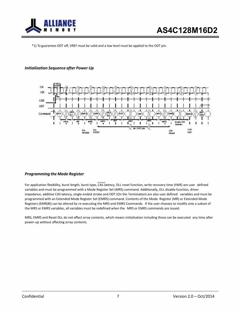
*1) To guarantee ODT off, VREF must be valid and a low level must be applied to the ODT pin.
Initialization Sequence after Power Up
Programming the Mode Register
For application flexibility, burst length, burst type, CAS latency, DLL reset function, write recovery time (tWR) are user defined
variables and must be programmed with a Mode Register Set (MRS) command. Additionally, DLL disable function, driver
impedance, additive CAS latency, single-ended strobe and ODT (On Die Termination) are also user defined variables and must be
programmed with an Extended Mode Register Set (EMRS) command. Contents of the Mode Register (MR) or Extended Mode
Registers (EMR(#)) can be altered by re-executing the MRS and EMRS Commands. If the user chooses to modify only a subset of
the MRS or EMRS variables, all variables must be redefined when the MRS or EMRS commands are issued.
MRS, EMRS and Reset DLL do not affect array contents, which means initialization including those can be executed any time after
power-up without affecting array contents.
AS4C128M16D2
Confidential 8 Version 2.0 – Oct/2014
AS4C128M16D2
Confidential 9 Version 2.0 – Oct/2014
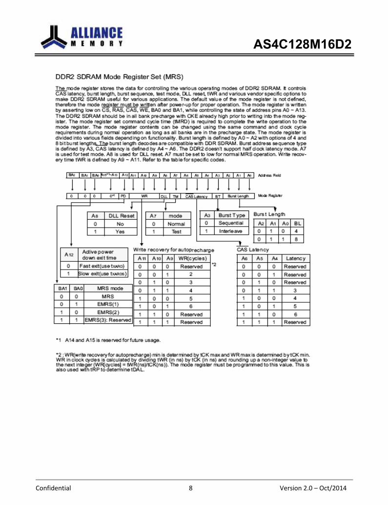
V59C1G02168QCP Rev.1.0 December 2012
DDR2 SDRAM Extended Mode Register Set
EMRS(1)
The extended mode register(1) stores the data for enabling or disabling the DLL, output driver strength, ODT value selection and additive latency. The default value of the extended mode register is not defined, therefore the extended mode register must be written after power-up for proper operation. Extended mode register(1) is written by asserting low on CS, RAS, CAS, WE and high on BA0 and low on BA1, and control-ling rest of pins A0 ~ A13.
The DDR2 SDRAM should be in all bank precharge with CKE already high prior to writing into the extended mode register. The mode register set command cycle time (tMRD) must be satisfied to complete the write operation to the extended mode register. Mode register contents can be changed using the same command and clock cycle requirements during normal operation as long as all banks are in the precharge state. A0 is used for DLL enable or disable. A1 is used for enabling reduced strength data-output drive. A3~A5 deter-mines the additive latency. A2 and A6 are used for ODT value selection, A7~A9 are used for OCD control, A10 is used for DQS disable and A11 is used for RDQS enable.
DLL Enable / Disable
The DLL must be enabled for normal operation. DLL enable is required during power up initialization, and upon returning to normal operation after having the DLL disabled. The DLL is automatically disabled when entering self refresh operation and is automatically re-enabled upon exit of self refresh operation. Any time the DLL is enabled (and subsequently reset), 200 clock cycles must occur before a Read command can be issued to allow time for the internal clock to be synchronized with the external clock. Failing to wait for syn-chronization to occur may result in a violation of the tAC or tDQSCK parameters.

AS4C128M16D2
Confidential 10 Version 2.0 – Oct/2014
A0 DLL En able
0 Enable
1 Disable
A5 A4 A3 Additive Latency
0 0 0 0
0 0 1 1
0 1 0 2
0 1 1 3
1 0 0 4
1 0 1 5
1 1 0 6
1 1 1 Reserved
A1 Output Driver
Impendence
Control
Driver
Size
0 Normal 100%
1 Weak 60%
A11
(RDQS Enable)
A10
(DQS Enable)
Strobe Function Matrix
RDQS/DM RDQS DQS DQS
0 (Disable) 0 (Enable) DM Hi-z DQS DQS
0 (Disable) 1 (Disable) DM Hi-z DQS Hi-z
1 (Enable) 0 (Enable) RDQS RDQS DQS DQS
1 (Enable) 1 (Disable) RDQS Hi-z DQS Hi-z
EMRS(1) Programming
BA2
BA1 BA0 A15*1~A13
A12
A11 A10 A9 A8 A7 A6 A5 A4 A3 A2 A1 A0
Address Field
0 0 1 0*1 Qoff RDQS DQS OCD program Rtt Additive latency
Rtt
D.I.C
DLL Extended Mode Register
BA1 BA0 MRS mode A6 A2 Rtt (NOMINAL)
0 0 MRS 0 0 ODT Disable
0 1 EMRS(1) 0 1 75 ohm
1 0 EMRS(2) 1 0 150 ohm
1 1 EMRS(3):Reserved 1 1 50 ohm
A9 A8 A7 OCD operation
0 0 0 OCD exit
0 0 1 Reserved
0 1 0 Reserved
1 0 0 Reserved
1 1 1 Enable OCD defaults *
* : After setting to default, OCD mode needs to be exited by setting A9-A7
to 000.
A12 Qoff (Optional) *
0 Output buffer enabled
1 Output buffer disabled
* : Outputs disabled - DQs, DQSs, DQSs, DQSs,
RDQS, RDQS. This feature is used in conjunction
with dimm IDD measurements when IDDQ is not
desired to be included.
A10 DQS
0 Enable
1 Disable
A11 RDQS Enable
0 Disable
1 Enable
* If RDQS is enabled, the
D M Function is disabled. RDQS is
active for reads and don’t care for
writes.
*1 : A14 and A15 is reserved for future usage.
AS4C128M16D2
Confidential 11 Version 2.0 – Oct/2014
0 1 1 0 *2 0*1
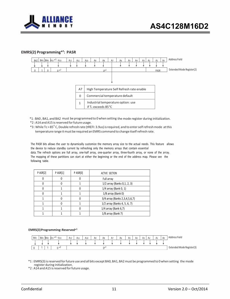
EMRS(2) Programming*¹: PASR
BA2 BA1 BA0 A15 *2 ~ A13
A12
A11 A10 A9 A8 A7 A6 A5 A4 A3 A2 A1 A0 Address Field
0 1 0 0 *2 0*1
PASR Extended Mode Register(2)
A7 High Temperature Self Refresh rate enable
0 Commercial temperature default
1 Industrial temperature option: use
if Tc exceeds 85 o C
*1 : BA0 , BA1, and BA2 must be programmed to 0 when setting the mode register during initialization. *2 : A14 and A15 is reserved for future usage.
*3 : While Tc > 85O
C, Double refresh rate (tREFI: 3.9us) is required, and to enter self refresh mode at this
temperature range it must be required an EMRS command to change itself refresh rate.
The PASR bits allows the user to dynamically customize the memory array size to the actual needs. This feature allows the device to reduce standby current by refreshing only the memory arrays that contain essential data. The refresh options are full array, one-half array, one-quarter array, three-fourth array, or none of the array. The mapping of these partitions can start at either the beginning or the end of the address map. Please see the following table.
P ASR[2] P ASR[1] P ASR[0] ACTIVE SECTION
0 0 0 Full array
0 0 1 1/2 array (Banks 0,1, 2, 3)
0 1 0 1/4 array (Bank 0, 1)
0 1 1 1/8 array (Bank 0)
1 0 0 3/4 array (Banks 2,3,4,5,6,7)
1 0 1 1/2 array (Banks 4, 5, 6, 7)
1 1 0 1/4 array (Bank 6,7)
1 1 1 1/8 array (Bank 7)
EMRS(3) Programming: Reserved*1
BA2 BA1 BA0 A15 *2 ~ A13 A12 A11 A10 A9 A8 A7 A6 A5 A4 A3 A2 A1 A0 Address Field
Extended Mode Register(3)
*1 : EMRS(3) is reserved for future use and all bits except BA0, BA1, BA2 must be programmed to 0 when setting the mode register during initialization.
*2 : A14 and A15 is reserved for future usage.

AS4C128M16D2
Confidential 12 Version 2.0 – Oct/2014
On-Die Termination (ODT)
On Die Termination (ODT) is a feature that allows a DRAM to turn on/off termination resistance for each DQ,
UDQS/UDQS, LDQS/LDQS, UDM and LDM via the ODT control pin. The ODT feature is designed to improve signal
integrity of the memory channel by allowing the DRAM controller to independently turn on/off termination
resistance for any or all DRAM devices.
The ODT function is supported for ACTIVE and STANDBY modes. ODT is turned off and not supported in SELF
REFRESH mode.
VDDQ VDDQ VDDQ
sw1
sw2
sw3
Rval1 Rval2 Rval3
DRAM Input
Buffer
Rval1
sw1
Rval2
sw2
Rval3
sw3
Input Pin
VSSQ VSSQ
Switch (sw1, sw2, sw3) is enabled by ODT pin.
VSSQ
Selection among sw1, sw2, and sw3 is determined by “Rtt (nominal)” in EMR. Termination
included on all DQs, UDQS/UDQS, LDQS/LDQS, UDM and LDM pins.
Functional representation of ODT

AS4C128M16D2
Confidential 13 Version 2.0 – Oct/2014
ODT Truth Table
The ODT Truth Table shows which of the input pins are terminated depending on the state of address bit A10and A11
in the EMRS.
To activate termination of any of these pins, the ODT function has to be enabled in the EMRS by address bits A6 and
A2.
X=Don’t Care 0=Signal Low 1=Signal High
AS4C128M16D2
Confidential 14 Version 2.0 – Oct/2014
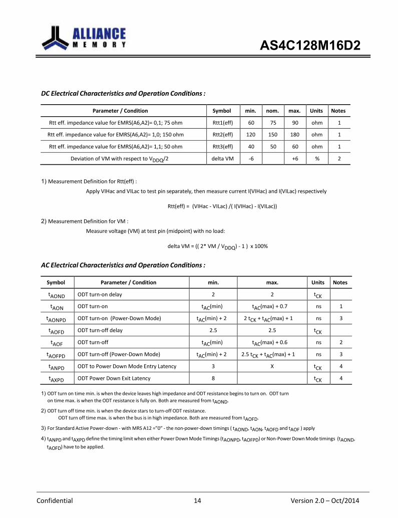
DC Electrical Characteristics and Operation Conditions :
Parameter / Condition Symbol min. nom. max. Units Notes
Rtt eff. impedance value for EMRS(A6,A2)= 0,1; 75 ohm Rtt1(eff) 60 75 90 ohm 1
Rtt eff. impedance value for EMRS(A6,A2)= 1,0; 150 ohm Rtt2(eff) 120 150 180 ohm 1
Rtt eff. impedance value for EMRS(A6,A2)= 1,1; 50 ohm Rtt3(eff) 40 50 60 ohm 1
Deviation of VM with respect to VDDQ/2 delta VM -6 +6 % 2
1) Measurement Definition for Rtt(eff) :
Apply VIHac and VILac to test pin separately, then measure current I(VIHac) and I(VILac) respectively
Rtt(eff) = (VIHac - VILac) /( I(VIHac) - I(VILac))
2) Measurement Definition for VM :
Measure voltage (VM) at test pin (midpoint) with no load:
delta VM = (( 2* VM / VDDQ) - 1 ) x 100%
AC Electrical Characteristics and Operation Conditions :
Symbol Parameter / Condition min. max. Units Notes
tAOND ODT turn-on delay 2 2 tCK
tAON ODT turn-on tAC(min) tAC(max) + 0.7 ns 1
tAONPD ODT turn-on (Power-Down Mode) tAC(min) + 2 2 tCK + tAC(max) + 1 ns 3
tAOFD ODT turn-off delay 2.5 2.5 tCK
tAOF ODT turn-off tAC(min) tAC(max) + 0.6 ns 2
tAOFPD ODT turn-off (Power-Down Mode) tAC(min) + 2 2.5 tCK + tAC(max) + 1 ns 3
tANPD ODT to Power Down Mode Entry Latency 3 X tCK 4
tAXPD ODT Power Down Exit Latency 8 tCK 4
1) ODT turn on time min. is when the device leaves high impedance and ODT resistance begins to turn on. ODT turn
on time max. is when the ODT resistance is fully on. Both are measured from tAOND.
2) ODT turn off time min. is when the device stars to turn-off ODT resistance.
ODT turn off time max. is when the bus is in high impedance. Both are measured from tAOFD.
3) For Standard Active Power-down - with MRS A12 =”0” - the non-power-down timings ( tAOND, tAON, tAOFD and tAOF ) apply
4) tANPD and tAXPD define the timing limit when either Power Down Mode Timings (tAONPD, tAOFPD) or Non-Power Down Mode timings (tAOND,
tAOFD) have to be applied.
AS4C128M16D2
Confidential 15 Version 2.0 – Oct/2014
ODT Timing for Active / Standby (Idle) Mode and Standard Active Power-Down Mode
T-n T-6 T-5 T-4 T-3 T-2 T-1 T0
CK, CK
CKE
t
IS
tAXPD
tIS
tANPD
t
IS
ODT t
IS tAOND tAOFD
DQ tAON(min)
Rtt tAOF(min)
tAON(max) tAOF(max) ODT1
1) Both ODT to Power Down Entry and Exit Latency timing parameter tANPD and tAXPD are met, therefore Non-Power Down Mode
timings have to be applied.
2) ODT turn-on time (tAON,min) is when the device leaves high impedance and ODT resistance begins to turn on. ODT turn on time max.
(tAON,max) is when the ODT resistance is fully on. Both are measured from tAOND.
3) ODT turn off time min. ( tAOF,min) is when the device starts to turn off the ODT resistance. ODT turn off time max. (tAOF,max) is when the
bus is in high impedance. Both are measured from tAOFD.
ODT Timing for Precharge Power-Down and Lo w Power Power -Down Mode
T-7 T-6 T-5 T-4 T-3 T-2 T-1 T0 T1
CK, CK
CKE tAXPD
tIS
tANPD
ODT
DQ
tIS
tAONPD,min
tAONPD,max
tAOFPD,min
tAOFPD,max
Rtt
ODT2
1) Both ODT to Power Down Entry and Exit Latencies tANPD and tAXPD are not met, therefore Power-Down Mode timings have to be applied.
AS4C128M16D2
Confidential 16 Version 2.0 – Oct/2014
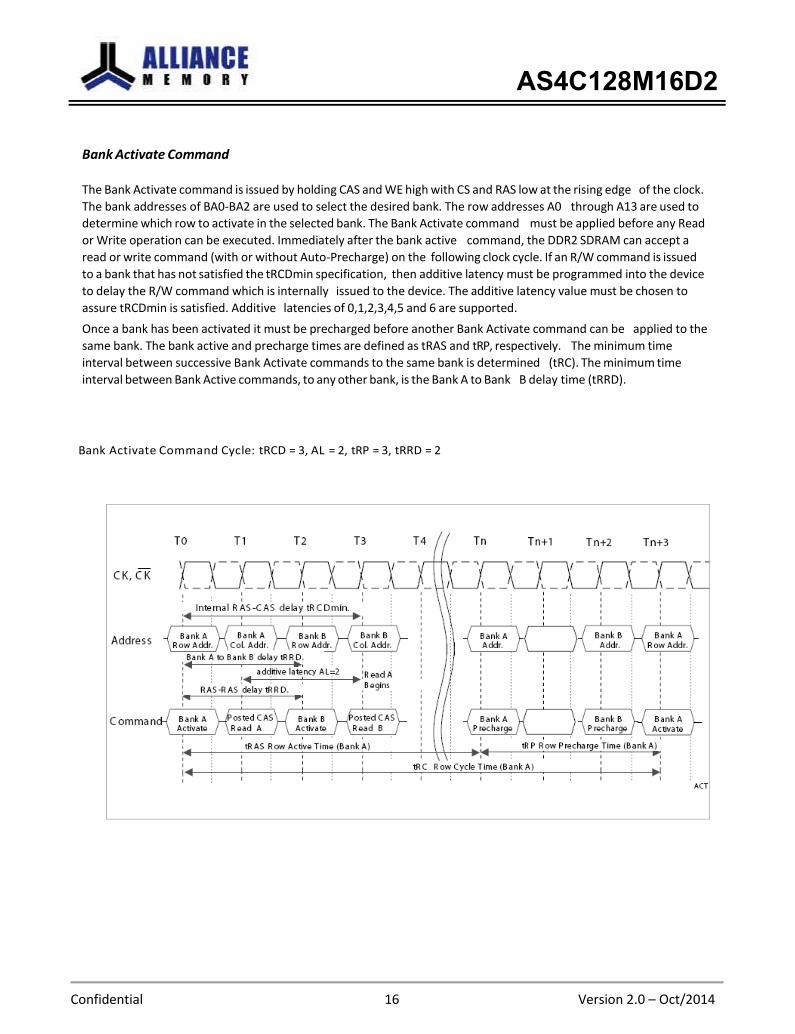
Bank Activate Command
The Bank Activate command is issued by holding CAS and WE high with CS and RAS low at the rising edge of the clock.
The bank addresses of BA0-BA2 are used to select the desired bank. The row addresses A0 through A13 are used to
determine which row to activate in the selected bank. The Bank Activate command must be applied before any Read
or Write operation can be executed. Immediately after the bank active command, the DDR2 SDRAM can accept a
read or write command (with or without Auto-Precharge) on the following clock cycle. If an R/W command is issued
to a bank that has not satisfied the tRCDmin specification, then additive latency must be programmed into the device
to delay the R/W command which is internally issued to the device. The additive latency value must be chosen to
assure tRCDmin is satisfied. Additive latencies of 0,1,2,3,4,5 and 6 are supported.
Once a bank has been activated it must be precharged before another Bank Activate command can be applied to the
same bank. The bank active and precharge times are defined as tRAS and tRP, respectively. The minimum time
interval between successive Bank Activate commands to the same bank is determined (tRC). The minimum time
interval between Bank Active commands, to any other bank, is the Bank A to Bank B delay time (tRRD).
Bank Activate Command Cycle: tRCD = 3, AL = 2, tRP = 3, tRRD = 2
AS4C128M16D2
Confidential 17 Version 2.0 – Oct/2014
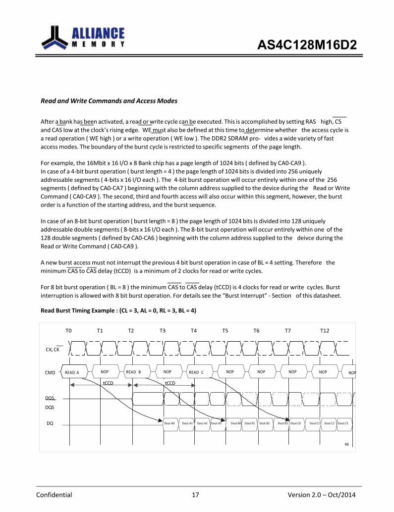
Read and Write Commands and Access Modes
After a bank has been activated, a read or write cycle can be executed. This is accomplished by setting RAS high, CS
and CAS low at the clock’s rising edge. WE must also be defined at this time to determine whether the access cycle is
a read operation ( WE high ) or a write operation ( WE low ). The DDR2 SDRAM pro- vides a wide variety of fast
access modes. The boundary of the burst cycle is restricted to specific segments of the page length.
For example, the 16Mbit x 16 I/O x 8 Bank chip has a page length of 1024 bits ( defined by CA0-CA9 ).
In case of a 4-bit burst operation ( burst length = 4 ) the page length of 1024 bits is divided into 256 uniquely
addressable segments ( 4-bits x 16 I/O each ). The 4-bit burst operation will occur entirely within one of the 256
segments ( defined by CA0-CA7 ) beginning with the column address supplied to the device during the Read or Write
Command ( CA0-CA9 ). The second, third and fourth access will also occur within this segment, however, the burst
order is a function of the starting address, and the burst sequence.
In case of an 8-bit burst operation ( burst length = 8 ) the page length of 1024 bits is divided into 128 uniquely
addressable double segments ( 8-bits x 16 I/O each ). The 8-bit burst operation will occur entirely within one of the
128 double segments ( defined by CA0-CA6 ) beginning with the column address supplied to the deivce during the
Read or Write Command ( CA0-CA9 ).
A new burst access must not interrupt the previous 4 bit burst operation in case of BL = 4 setting. Therefore the
minimum CAS to CAS delay (tCCD) is a minimum of 2 clocks for read or write cycles.
For 8 bit burst operation ( BL = 8 ) the minimum CAS to CAS delay (tCCD) is 4 clocks for read or write cycles. Burst
interruption is allowed with 8 bit burst operation. For details see the “Burst Interrupt” - Section of this datasheet.
Read Burst Timing Example : (CL = 3, AL = 0, RL = 3, BL = 4)
T0 T1 T2 T3 T4 T5 T6 T7 T12
CK, CK
CMD READ A NOP READ B NOP READ C NOP NOP NOP NOP NOP
tCCD tCCD
DQS,
DQS
DQ Dout A0 Dout A1 Dout A2 Dout A3 Dout B0 Dout B1 Dout B2 Dout B3 Dout C0 Dout C1 Dout C2 Dout C3
RB
AS4C128M16D2
Confidential 18 Version 2.0 – Oct/2014
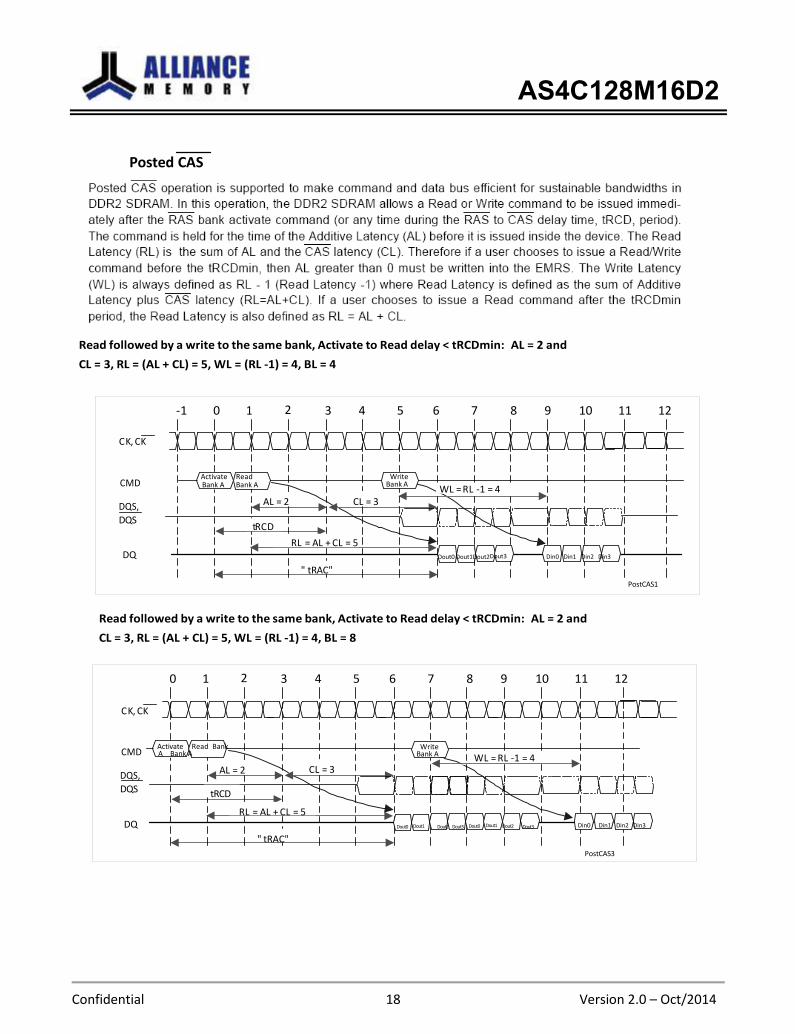
Posted CAS
Read followed by a write to the same bank, Activate to Read delay < tRCDmin: AL = 2 and
CL = 3, RL = (AL + CL) = 5, WL = (RL -1) = 4, BL = 4
-1 0 1 2 3 4 5 6 7 8 9 10 11 12
CK, CK
CMD
Activate Read W rite Bank A Bank A Bank A
WL = RL -1 = 4
DQS,
DQS
AL = 2
tRCD
CL = 3
RL = AL + CL = 5 DQ
" tRAC"
Dout0 Dout1 Dout2Dout3
Din0 Din1 Din2 Din3
PostCAS1
Read followed by a write to the same bank, Activate to Read delay < tRCDmin: AL = 2 and
CL = 3, RL = (AL + CL) = 5, WL = (RL -1) = 4, BL = 8
0 1 2 3 4 5 6 7 8 9 10 11 12
CK, CK
CMD
DQS,
DQS
Activate Read Bank A Bank A
AL = 2
tRCD
CL = 3
W rite
Bank A
WL = RL -1 = 4
RL = AL + CL = 5 DQ
" tRAC"
Dout0 Dout1 Dout2 Dout3 Dout0 Dout1 Dout2 Dout3
Din0 Din1 Din2 Din3
PostCAS3

AS4C128M16D2
Confidential 19 Version 2.0 – Oct/2014
Read followed by a write to the same bank, Activate to Read delay > tRCDmin: AL = 1, CL
= 3, RL = 4, WL = 3, B L = 4
-1 0 1 2 3 4 5 6 7 8 9 10 11 12
CK, CK
CMD
DQS,
DQS
Activate Bank A
tRCD>tRCDmin.
Read Bank A
RL = 4
W rite
Bank A
WL = 3
DQ
"tRAC" Dout0 Dout1 Dout2 Dout3 Din0 Din1 Din2 Din3
PostCAS5
AS4C128M16D2
Confidential 20 Version 2.0 – Oct/2014
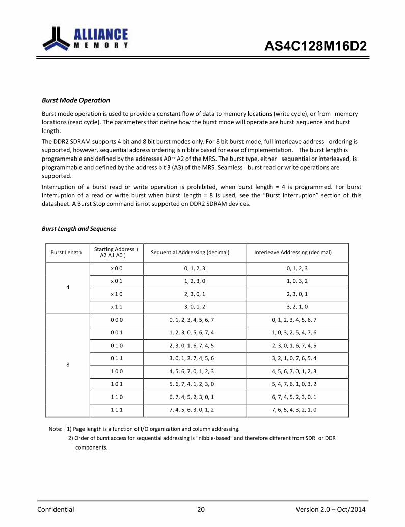
Burst Mode Operation
Burst mode operation is used to provide a constant flow of data to memory locations (write cycle), or from memory
locations (read cycle). The parameters that define how the burst mode will operate are burst sequence and burst
length.
The DDR2 SDRAM supports 4 bit and 8 bit burst modes only. For 8 bit burst mode, full interleave address ordering is
supported, however, sequential address ordering is nibble based for ease of implementation. The burst length is
programmable and defined by the addresses A0 ~ A2 of the MRS. The burst type, either sequential or interleaved, is
programmable and defined by the address bit 3 (A3) of the MRS. Seamless burst read or write operations are
supported.
Interruption of a burst read or write operation is prohibited, when burst length = 4 is programmed. For burst
interruption of a read or write burst when burst length = 8 is used, see the “Burst Interruption” section of this
datasheet. A Burst Stop command is not supported on DDR2 SDRAM devices.
Burst Length and Sequence
Burst Length Starting Address (
A2 A1 A0 ) Sequential Addressing (decimal) Interleave Addressing (decimal)
4
x 0 0 0, 1, 2, 3 0, 1, 2, 3
x 0 1 1, 2, 3, 0 1, 0, 3, 2
x 1 0 2, 3, 0, 1 2, 3, 0, 1
x 1 1 3, 0, 1, 2 3, 2, 1, 0
8
0 0 0 0, 1, 2, 3, 4, 5, 6, 7 0, 1, 2, 3, 4, 5, 6, 7
0 0 1 1, 2, 3, 0, 5, 6, 7, 4 1, 0, 3, 2, 5, 4, 7, 6
0 1 0 2, 3, 0, 1, 6, 7, 4, 5 2, 3, 0, 1, 6, 7, 4, 5
0 1 1 3, 0, 1, 2, 7, 4, 5, 6 3, 2, 1, 0, 7, 6, 5, 4
1 0 0 4, 5, 6, 7, 0, 1, 2, 3 4, 5, 6, 7, 0, 1, 2, 3
1 0 1 5, 6, 7, 4, 1, 2, 3, 0 5, 4, 7, 6, 1, 0, 3, 2
1 1 0 6, 7, 4, 5, 2, 3, 0, 1 6, 7, 4, 5, 2, 3, 0, 1
1 1 1 7, 4, 5, 6, 3, 0, 1, 2 7, 6, 5, 4, 3, 2, 1, 0
Note: 1) Page length is a function of I/O organization and column addressing.
2) Order of burst access for sequential addressing is “nibble-based” and therefore different from SDR or DDR
components.
AS4C128M16D2
Confidential 21 Version 2.0 – Oct/2014
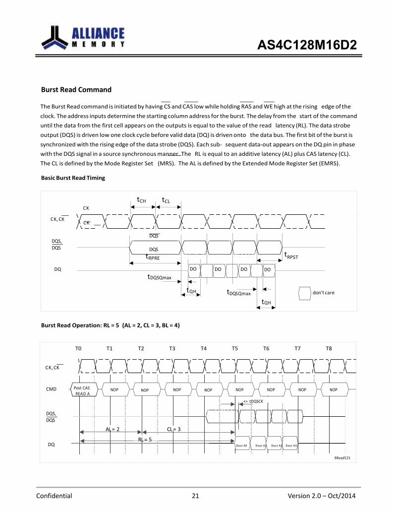
Burst Read Command
The Burst Read command is initiated by having CS and CAS low while holding RAS and WE high at the rising edge of the
clock. The address inputs determine the starting column address for the burst. The delay from the start of the command
until the data from the first cell appears on the outputs is equal to the value of the read latency (RL). The data strobe
output (DQS) is driven low one clock cycle before valid data (DQ) is driven onto the data bus. The first bit of the burst is
synchronized with the rising edge of the data strobe (DQS). Each sub- sequent data-out appears on the DQ pin in phase
with the DQS signal in a source synchronous manner. The RL is equal to an additive latency (AL) plus CAS latency (CL).
The CL is defined by the Mode Register Set (MRS). The AL is defined by the Extended Mode Register Set (EMRS).
Basic Burst Read Timing
CK, CK
CK
CK
tCH tCL
DQS,
DQS
DQ
DQS
DQS
tRPRE
tDQSQmax
DO DO DO DO
tRPST
tQH tDQSQmax
tQH
don’t care
Burst Read Operation: RL = 5 (AL = 2, CL = 3, BL = 4)
T0 T1 T2 T3 T4 T5 T6 T7 T8
CK, CK
CMD Post CAS
REA D A
NOP
NOP
NOP
NOP
NOP NOP NOP NOP
<= tDQSCK
DQS,
DQS
DQ
AL = 2 CL = 3
RL = 5
Dou t A0 Dout A1 Dou t A2 Dout A3
BRead523
AS4C128M16D2
Confidential 22 Version 2.0 – Oct/2014
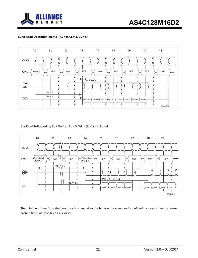
Burst Read Operation: RL = 3 (AL = 0, CL = 3, BL = 8)
T0 T1 T2 T3 T4 T5 T6 T7 T8
CK, CK
CMD READ A NOP NOP NOP NOP NOP NOP NOP NOP
DQS,
DQS
<= tDQSCK
DQ’s
CL = 3
RL = 3
Dout A0 Dout A1 Dout A2 Dout A3 Dout A4 Dout A5 Dout A6 Dout A7
BRead303
Burst Read followed by Burst Write : RL = 5, WL = (RL -1) = 4, B L = 4
T0 T1 T3 T4 T5 T6 T7 T8 T9
CK, CK
CMD
DQS,
DQS
Posted CAS R EAD A
NOP
BL/2 + 2
NOP Posted CAS
WR ITE A
NOP
NOP NOP NOP NOP
RL = 5
DQ
WL = RL - 1 = 4
Dout A0 Dout A1 Dout A2 Dout A3
Din A0 Din A1 Din A2 Din A3
BRBW514
The minimum time from the burst read command to the burst write command is defined by a read-to-write turn-
around time, which is BL/2 + 2 clocks.
AS4C128M16D2
Confidential 23 Version 2.0 – Oct/2014
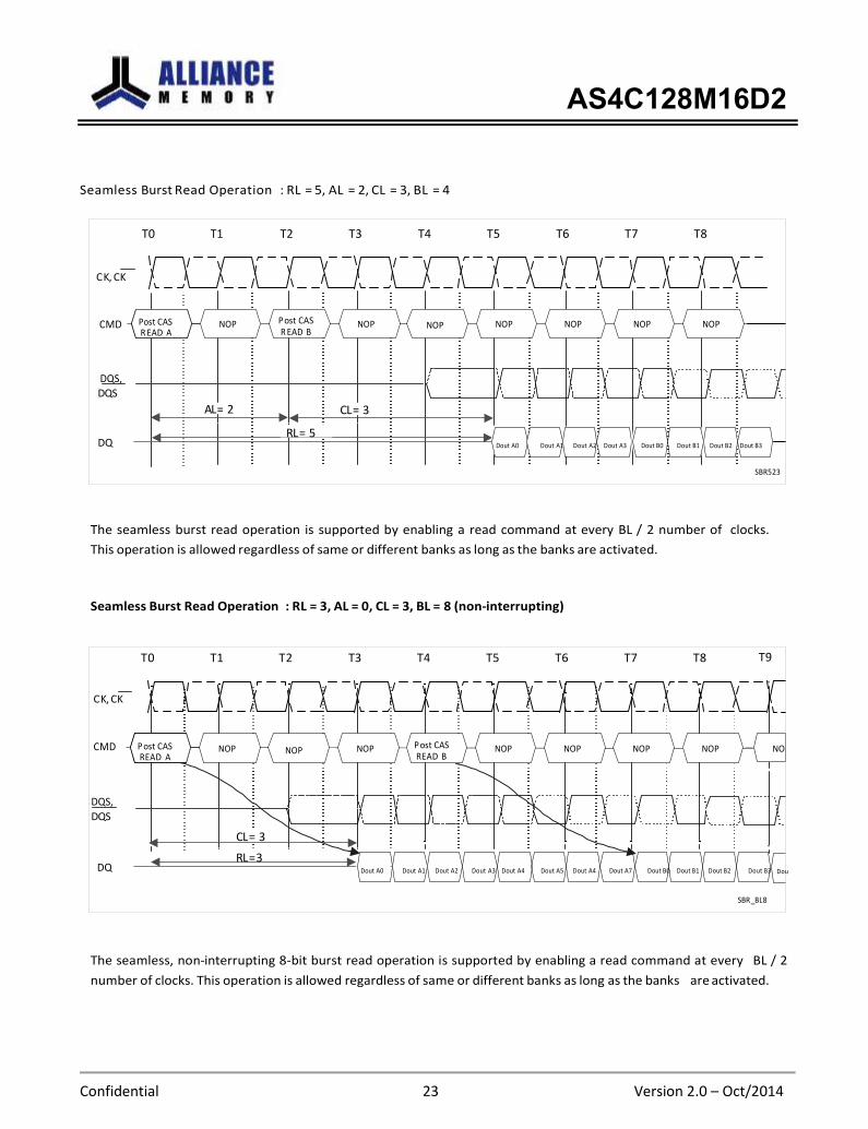
Seamless Burst Read Operation : R L = 5, AL = 2, CL = 3, BL = 4
T0 T1 T2 T3 T4 T5 T6 T7 T8
CK, CK
CMD Post CAS R EAD A
NOP P ost CAS R EAD B
NOP
NOP
NOP NOP NOP NOP
DQS,
DQS
DQ
AL = 2 CL = 3
RL = 5
Dout A0 Dout A1 Dout A2 Dout A3 Dout B0 Dout B1 Dout B2 Dout B3
SBR523
The seamless burst read operation is supported by enabling a read command at every BL / 2 number of clocks.
This operation is allowed regardless of same or different banks as long as the banks are activated.
Seamless Burst Read Operation : RL = 3, AL = 0, CL = 3, BL = 8 (non-interrupting)
T0 T1 T2 T3 T4 T5 T6 T7 T8 T9
CK, CK
CMD P ost CAS READ A
NOP
NOP
NOP P ost CAS READ B
NOP NOP NOP NOP NO
DQS,
DQS
DQ
CL = 3
RL = 3
Dout A0 Dout A1 Dout A2 Dout A3 Dout A4 Dout A5 Dout A4 Dout A7 Dout B0 Dout B1 Dout B2 Dout B3 Dou
SBR_BL8
The seamless, non-interrupting 8-bit burst read operation is supported by enabling a read command at every BL / 2
number of clocks. This operation is allowed regardless of same or different banks as long as the banks are activated.

AS4C128M16D2
Confidential 24 Version 2.0 – Oct/2014
Burst Write Command
The Burst Write command is initiated by having CS, CAS and WE low while holding RAS high at the rising edge of
the clock. The address inputs determine the starting column address. Write latency (WL) is defined by a read latency
(RL) minus one and is equal to (AL + CL -1). A data strobe signal (DQS) should be driven low (preamble) one clock
prior to the WL. The first data bit of the burst cycle must be applied to the DQ pins at the first rising edge of the DQS
following the preamble. The tDQSS specification must be satisfied for write cycles. The subsequent burst bit data are
issued on successive edges of the DQS until the burst length is completed. When the burst has finished, any
additional data supplied to the DQ pins will be ignored. The DQ signal is ignored after the burst write operation is
complete. The time from the completion of the burst write to bank precharge is named “write recovery time” (tWR)
and is the time needed to store the write data into the memory array. tWR is an analog timing parameter (see the AC
table in this specification) and is not the programmed value for WR in the MRS.
Basic Burst Write Timing
t DQSH tDQSL
DQS,
DQS
DQS DQS
t WPRE
t WPST
Din Din Din Din
t DS t DH
Burst Write Operation : RL = 5 (AL = 2, CL = 3), WL = 4, BL = 4
T0 T1 T2 T3 T4 T5 T6 T7 Tn
CK, CK
CMD Post CAS WRITE A
NOP
NOP NOP NOP NOP NOP NOP Precharge
DQS,
DQS
DQ
WL = RL-1 = 4
<= tDQSS
DIN A0 DIN A1 DIN A2 DIN A3
Completion of
the Burst Write
tWR

AS4C128M16D2
Confidential 25 Version 2.0 – Oct/2014
Burst Write Operation : RL = 3 (AL = 0, CL = 3), WL = 2, BL = 4
T0 T1 T2 T3 T4 T5 T6 Tm Tn
CK, CK
CMD
Post CAS WRITE A
NOP
NOP
NOP
NOP
NOP NOP
Bank A
Precharge Activate
DQS,
DQS
DQ
WL = RL-1 = 2
<= tDQSS
DIN A0 DIN A1 DIN A2 DIN A3
Completion of
the Burst Write
tWR
tRP
Burst Write followed by Burst Read : RL = 5 (AL = 2, CL = 3), WL = 4, tWTR = 2, BL = 4
T0 T1 T2 T3 T4 T5 T6 T7 T8 T9
CK, CK
Write to Read = (CL - 1)+ BL/2 +tWTR(2) = 6
CMD
NOP
NOP
NOP
NOP Post CAS
READ A
NOP
NOP
NOP
NOP
DQS,
DQS
DQ
WL = RL - 1 = 4
DIN A0 DIN A1 DIN A2 DIN A3
AL=2 CL=3
tWTR
RL=5
The minimum number of clocks from the burst write command to the burst read command is
(CL - 1) +BL/2 + tWTR
where tWTR is the write-to-read turn-around time tWTR expressed in clock cycles. The tWTR is not a write recovery
time (tWR) but the time required to transfer 4 bit write data from the input buffer into sense amplifiers in the array.
AS4C128M16D2
Confidential 26 Version 2.0 – Oct/2014
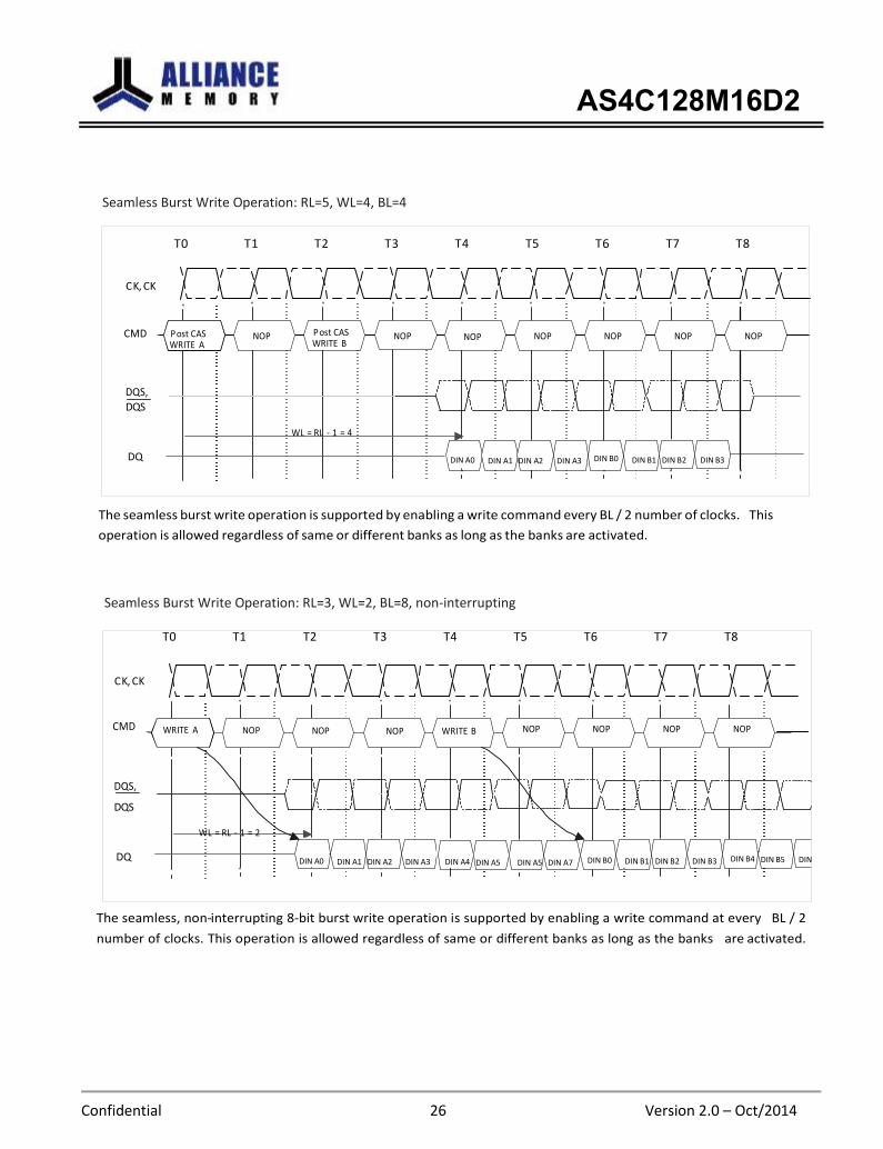
Seamless Burst Write Operation: RL=5, WL=4, BL=4
T0 T1 T2 T3 T4 T5 T6 T7 T8
CK, CK
CMD P ost CAS WR ITE A
NOP P ost CAS WR ITE B
NOP
NOP
NOP NOP NOP NOP
DQS,
DQS
WL = RL - 1 = 4
DQ
DIN A0 DIN A1 DIN A2 DIN A3 DIN B0 DIN B1 DIN B2 DIN B3
The seamless burst write operation is supported by enabling a write command every BL / 2 number of clocks. This
operation is allowed regardless of same or different banks as long as the banks are activated.
Seamless Burst Write Operation: RL=3, WL=2, BL=8, non-interrupting
T0 T1 T2 T3 T4 T5 T6 T7 T8
CK, CK
CMD
WR ITE A
NOP
NOP
NOP
WR ITE B
NOP NOP NOP NOP
DQS,
DQS
WL = RL - 1 = 2
DQ
DIN A0 DIN A1 DIN A2 DIN A3 DIN A4 DIN A5 DIN A5 DIN A7 DIN B0 DIN B1 DIN B2 DIN B3 DIN B4 DIN B5 DIN
The seamless, non-interrupting 8-bit burst write operation is supported by enabling a write command at every BL / 2
number of clocks. This operation is allowed regardless of same or different banks as long as the banks are activated.
AS4C128M16D2
Confidential 27 Version 2.0 – Oct/2014
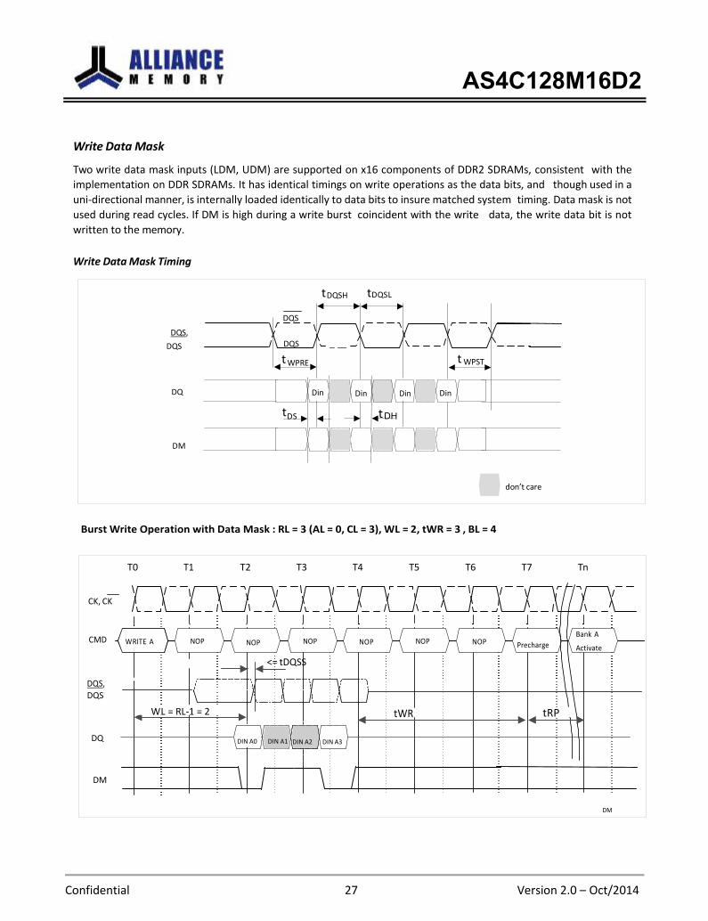
Write Data Mask
Two write data mask inputs (LDM, UDM) are supported on x16 components of DDR2 SDRAMs, consistent with the
implementation on DDR SDRAMs. It has identical timings on write operations as the data bits, and though used in a
uni-directional manner, is internally loaded identically to data bits to insure matched system timing. Data mask is not
used during read cycles. If DM is high during a write burst coincident with the write data, the write data bit is not
written to the memory.
Write Data Mask Timing
t DQSH tDQSL
DQS,
DQS
DQS DQS
t WPRE
t WPST
DQ Din
tDS
Din Din
t
Din
DM
don’t care
Burst Write Operation with Data Mask : RL = 3 (AL = 0, CL = 3), WL = 2, tWR = 3 , BL = 4
T0 T1 T2 T3 T4 T5 T6 T7 Tn
CK, CK
CMD
WRITE A
NOP
NOP
NOP
NOP
NOP NOP
Bank A
Precharge Activate
<= tDQSS
DQS,
DQS
WL = RL-1 = 2
tWR
tRP
DQ DIN A0 DIN A1 DIN A2
DIN A3
DM
DM
AS4C128M16D2
Confidential 28 Version 2.0 – Oct/2014
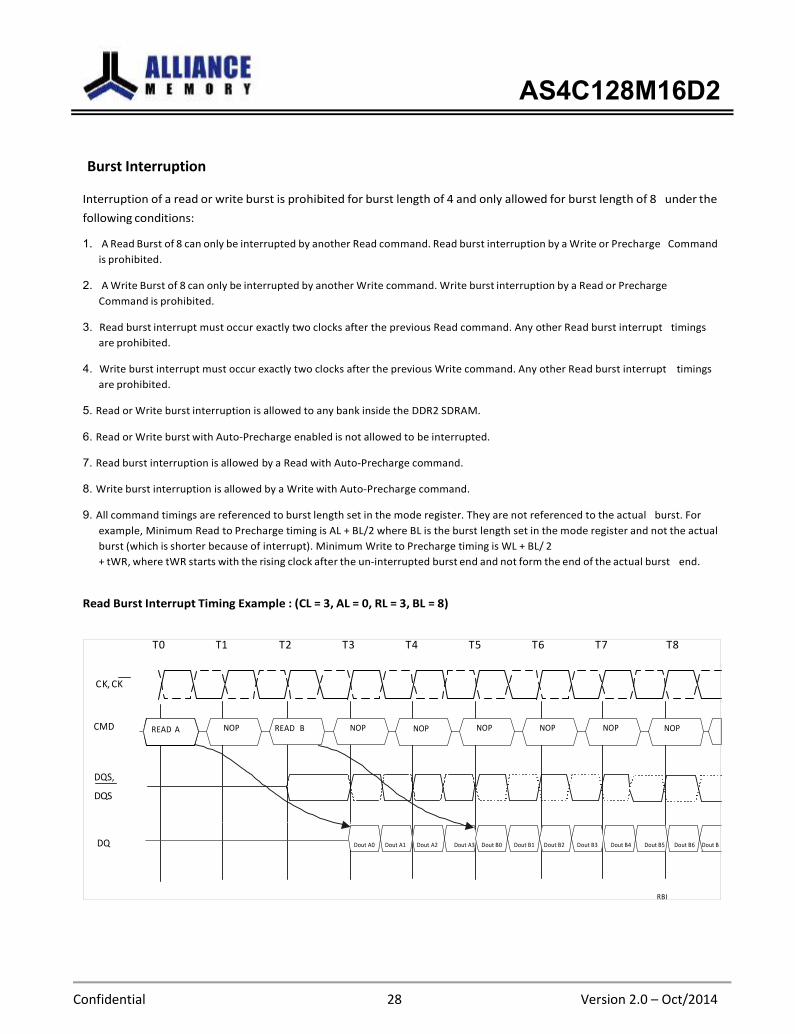
Burst Interruption
Interruption of a read or write burst is prohibited for burst length of 4 and only allowed for burst length of 8 under the
following conditions:
1. A Read Burst of 8 can only be interrupted by another Read command. Read burst interruption by a Write or Precharge Command
is prohibited.
2. A Write Burst of 8 can only be interrupted by another Write command. Write burst interruption by a Read or Precharge
Command is prohibited.
3. Read burst interrupt must occur exactly two clocks after the previous Read command. Any other Read burst interrupt timings
are prohibited.
4. Write burst interrupt must occur exactly two clocks after the previous Write command. Any other Read burst interrupt timings
are prohibited.
5. Read or Write burst interruption is allowed to any bank inside the DDR2 SDRAM.
6. Read or Write burst with Auto-Precharge enabled is not allowed to be interrupted.
7. Read burst interruption is allowed by a Read with Auto-Precharge command.
8. Write burst interruption is allowed by a Write with Auto-Precharge command.
9. All command timings are referenced to burst length set in the mode register. They are not referenced to the actual burst. For
example, Minimum Read to Precharge timing is AL + BL/2 where BL is the burst length set in the mode register and not the actual
burst (which is shorter because of interrupt). Minimum Write to Precharge timing is WL + BL/ 2
+ tWR, where tWR starts with the rising clock after the un-interrupted burst end and not form the end of the actual burst end.
Read Burst Interrupt Timing Example : (CL = 3, AL = 0, RL = 3, BL = 8)
T0 T1 T2 T3 T4 T5 T6 T7 T8
CK, CK
CMD
READ A NOP READ B NOP NOP NOP NOP NOP NOP
DQS,
DQS
DQ Dout A0 Dout A1 Dout A2 Dout A3 Dout B0 Dout B1 Dout B2 Dout B3 Dout B4 Dout B5 Dout B6 Dout B
RBI
AS4C128M16D2
Confidential 29 Version 2.0 – Oct/2014
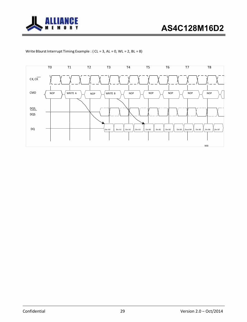
Write B burst Interrupt Timing Example : ( CL = 3, AL = 0, WL = 2, BL = 8)
T0 T1 T2 T3 T4 T5 T6 T7 T8
CK, CK
CMD NOP WR ITE A
NOP
WR ITE B NOP NOP NOP NOP NOP
DQS,
DQS
DQ Din A0 Din A1 Din A2 Din A3 Din B0 Din B1 Din B2 Din B3 Dout B4 Din B5 Din B6 Din B7
WBI

AS4C128M16D2
Confidential 30 Version 2.0 – Oct/2014
A10
B A 0
B A1
B A2
Precharge
Bank(s)
LOW HIGH LOW HIGH Bank 5 only
LOW LOW HIGH HIGH Bank 6 only
LOW HIGH HIGH HIGH Bank 7 only
HIGH Don't Care Don't Care Don't Care All Banks
Precharge Command
The Precharge Command is used to precharge or close a bank that has been activated. The Precharge Command is
triggered when CS, RAS and WE are low and CAS is high at the rising edge of the clock. The Pre-charge Command can
be used to precharge each bank independently or all banks simultaneously. Four address bits A10, BA2, BA1 and
BA0 are used to define which bank to precharge when the command is issued.
Bank Selection for Precharge by Address Bits
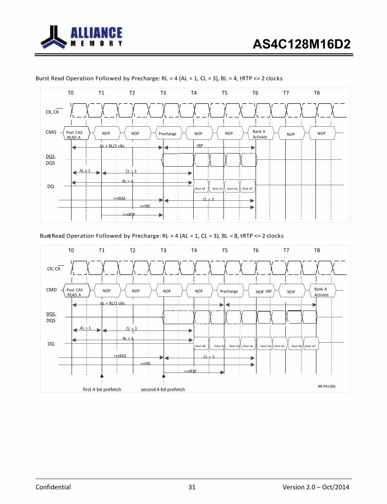
Burst Read Operation Followed by a Precharge
The following rules apply as long as the tRTP timing parameter - Internal Read to Precharge Command delay time - is
less or equal two clocks, which is the case for operating frequencies less or equal 266 MHz (DDR2 400 and 533 speed
sorts):
Minimum Read to Precharge command spacing to the same bank = AL + BL/2 clocks. For the earliest possible
precharge, the precharge command may be issued on the rising edge which is “Additive Latency (AL) + BL/2 clocks”
after a Read Command, as long as the minimum tRAS timing is satisfied.
A new bank active command may be issued to the same bank if the following two conditions are satisfied
simultaneously:
(1) The RAS precharge time (tRP) has been satisfied from the clock at which the precharge begins.
(2) The RAS cycle time (tRCmin) from the previous bank activation has been satisfied.
For operating frequencies higher than 266 MHz, tRTP becomes > 2 clocks and one additional clock cycle has to be
added for the minimum Read to Precharge command spacing, which now becomes AL + BL/2 + 1 clocks.
A10
B A 0
B A1
B A2
Precharge Bank(s)
LOW LOW LOW LOW Bank 0 only
LOW HIGH LOW LOW Bank 1 only
LOW LOW HIGH LOW Bank 2 only
LOW HIGH HIGH LOW Bank 3 only
LOW LOW LOW HIGH Bank 4 only
AS4C128M16D2
Confidential 31 Version 2.0 – Oct/2014
Burst Read Operation Followed by Precharge: RL = 4 (AL = 1, CL = 3), BL = 4, tRTP <= 2 clocks
T0 T1 T2 T3 T4 T5 T6 T7 T8
CK, CK
CMD
DQS,
DQS
Post CAS READ A
NOP
AL + BL/2 clks
NOP
Precharge
NOP
tRP
NOP Bank A Activate
NOP
NOP
AL = 1 CL = 3
RL = 4
DQ
Dout A0 Dout A1 Dout A2 Dout A3
>=tRAS CL = 3
>=tRC
>=tRTP
Burst Read Operation Followed by Precharge: RL = 4 (AL = 1, CL = 3), BL = 8, tRTP <= 2 cl ock s
T0 T1 T2 T3 T4 T5 T6 T7 T8
CK, CK
CMD
DQS,
DQS
Post CAS READ A
NOP
AL + BL/2 clks
NOP
NOP NOP
Precharge NOP tRP
NOP
Bank A
Activate
AL = 1 CL = 3
RL = 4
DQ
Dout A0 Dout A1 Dout A2 Dout A3
Dout A4 Dout A5 Dout A6 Dout A7
>=tRAS CL = 3
>=tRC
>=tRTP
first 4-bit prefetch second 4-bit prefetch BR-P413(8)

AS4C128M16D2
Confidential 32 Version 2.0 – Oct/2014
Burst Read operation Followed by Precharge: RL=5(AL=2, CL=3), BL=4, tRTP<=2 clocks
T0 T1 T2 T3 T4 T5 T6 T7 T8
CK, CK
CMD
P ost CAS R EAD A
NOP
AL + BL/2 clks
NOP
NOP
Precharge NOP NOP
Bank A
Activate
tRP
NOP
DQS,
DQS
AL = 2 CL = 3
RL = 5
DQ
>=tRAS CL = 3
>=tRC
>=tRTP
Dout A0 Dout A1 Dout A2 Dout A3
BR-P523
Burst Read operation Followed by Precharge: RL=6(AL=2, CL=4), BL=4, tRTP<=2 clocks
T0 T1 T2 T3 T4 T5 T6 T7 T8
CK, CK
CMD
P ost CAS R EAD A
NOP
AL + BL/2 clocks
NOP
NOP Precharge
A
NOP
tRP
NOP
NOP
Bank A
Activate
DQS,
DQS
DQ
AL = 2
RL = 6
CL = 4
Dout A0 Dout A1 Dout A2 Dout A3
>=tRAS CL = 4
>=tRC
>=tRTP
BR-P624
AS4C128M16D2
Confidential 33 Version 2.0 – Oct/2014
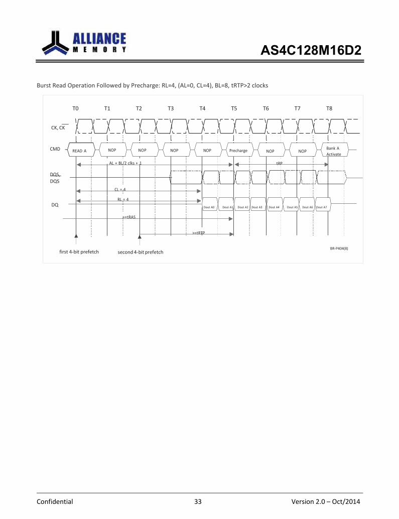
Burst Read Operation Followed by Precharge: RL=4, (AL=0, CL=4), BL=8, tRTP>2 clocks
T0 T1 T2 T3 T4 T5 T6 T7 T8
CK, CK
CMD
READ A
NOP
NOP
NOP NOP
Precharge NOP
NOP
Bank A
Activate
AL + BL/2 clks + 1 tRP
DQS,
DQS
CL = 4
RL = 4
DQ
>=tRAS
Dout A0 Dout A1 Dout A2 Dout A3
Dout A4 Dout A5 Dout A6 Dout A7
>=tRTP
first 4-bit prefetch second 4-bit prefetch BR-P404(8)

AS4C128M16D2
Confidential 34 Version 2.0 – Oct/2014
Burst Write followed by Precharge Minimum Write to Precharge command spacing to the same bank = WL + BL/2 + tWR. For write cycles, a delay
must be satisfied from the completion of the last burst write cycle until the Precharge command can be issued. This
delay is known as a write recovery time (t WR ) referenced from the completion of the burst write to the Precharge
command. No Precharge command should be issued prior to the tWR delay, as DDR2 SDRAM does not support
any burst interrupt by a Precharge command. tWR is an analog timing parameter (see the AC table in this datasheet)
and is not the programmed value for tWR in the MRS.
Burst Write followed by Precharge : WL = (RL - 1) = 3, BL = 4, tWR = 3
T0 T1 T2 T3 T4 T5 T6 T7 T8
CK, CK
CMD
DQS,
DQS
Post CAS WR ITE A
NOP
WL = 3
NOP
NOP
NOP
NOP NOP NOP
Completion of
the Burs t Write
tWR
P recharge
A
DQ DIN A0 DIN A1 DIN A2 DIN A3
BW -P3
B urs t Write followed by Prec harge : WL = (R L - 1) = 4, BL = 4, tWR = 3
T0 T1 T2 T3 T4 T5 T6 T7 T9
CK, CK
CMD Post CAS WR ITE A
NOP
NOP
NOP
NOP
NOP
NOP
NOP Precharge
A
DQS,
DQS
DQ
WL =4
DIN A0 DIN A1 DIN A2 DIN A3
Completion of
the Burs t Write
tWR
BW -P4
AS4C128M16D2
Confidential 35 Version 2.0 – Oct/2014
Au to-Precharge Operation
Before a new row in an active bank can be opened, the active bank must t be precharged using either the Pre- charge
Command or the Auto-Precharge function. When a Read or a Write Command is given to the DDR2 SDRAM, the CAS
timing accepts one extra address, column address A10, to allow the active bank to automatically begin precharge a t
the earliest possible moment during the burs t read or write cycle. If A10 is low when the Read or Write Command is
issued, then normal Read or Write burs t operation is executed and the bank remains active at the completion of the
burs t sequence. If A10 is high when the Read or Write Command is issued, then the Auto-Precharge function is
enabled. During Auto-Precharge, a Read Command will execute as normal with the exception that the active bank will
begin to precharge internally on the rising edge which is CAS Latency (CL) clock cycles before the end of the read burs t.
Auto-Precharge is also implemented for Write Commands. The precharge operation engaged by the Auto-Precharge
command will not begin until the last data of the write burst sequence is properly stored in the memory array. This
feature allows the pre- charge operation to be partially or completely hidden during burst read cycles (dependent upon
CAS Latency) thus improving system performance for random data access. The RAS lockout circuit internally delays
the Precharge operation until the array res tore operation has been completed so that the Auto-Precharge command
may be issued with any read or write command.
B urs t Read w ith A u to-P recharge
If A10 is high when a Read Command is issued, the Read with Auto-Precharge function is engaged. The DDR2
SDRAM s tarts an Auto-Precharge operation on the rising edge which is (AL + BL/2) cycles later from the Read with AP
command if tRAS(min) and tRTP are satisfied. If tRAS(min) is not satisfied at the edge, the s tart point of Auto-
Precharge operation will be delayed until tRAS(min) is satisfied. If tRTP(min) is not satisfied a t the edge, the s tart point
of Auto-precharge operation will be delayed until tRTP(min) is satisfied.
In case the internal precharge is pushed out by tRTP, tRP s tarts at the point where the internal precharge happens
(not a t the next rising clock edge after this event). So for BL = 4 the minimum time from Read with Auto-P recharge to
the next Activate command becomes AL + tRTP + tRP. F or BL = 8 the time from Read with Auto-P recharge to the next
Activate command is AL + 2 + tRTP + tRP. Note that t both parameters tRTP and tRP have to be rounded up to the
next integer value. In any event internal precharge does not s tart earlier than two clocks after the last t 4-bit
prefetch.
A new bank active (command) may be issued to the same bank if the following two conditions are satisfied
simultaneously:
(1) The RAS precharge time (tRP) has been satisfied from the clock at which the Auto-Precharge begins.
(2) The RAS cycle time (tRC) from the previous bank activation has been satisfied.

AS4C128M16D2
Confidential 36 Version 2.0 – Oct/2014
Burst Read with A u to-Precharge followed by an activation to the Same Bank (tRC Limit) RL = 5 (AL = 2,
CL = 3), BL = 4, tRTP <= 2 c locks
T0 T1 T2 T3 T4 T5 T6 T7 T8
CK, CK
CMD P osted CAS READ w/AP
A10 ="high"
NOP
NOP
NOP
NOP
NOP NOP
NOP Bank
Activate
DQS,
DQS
AL + BL/2 Auto-P recharge Begins
AL = 2 CL = 3
RL = 5 DQ
tRAS
tRCmin.
tRP
Dout A0 Dout A1 Dout A2 Dout A3
BR-AP5231
B urs t Read with A u to-Precharge followed by an Activation to the Same B ank (tRAS L imi t): RL = 5 ( AL
= 2, CL = 3), BL = 4, tRTP <= 2 c locks
T0 T1 T2 T3 T4 T5 T6 T7 T8
CK, CK
CMD P osted CAS READ w/AP
A10 ="high"
NOP
NOP
NOP
NOP
NOP NOP Bank
Activate
NOP
DQS,
DQS
tRAS(min) Auto-P recharge Begins
AL = 2 CL = 3
RL = 5 DQ
tRP
Dout A0 Dout A1 Dout A2 Dout A3
tRC
BR-AP5232
AS4C128M16D2
Confidential 37 Version 2.0 – Oct/2014
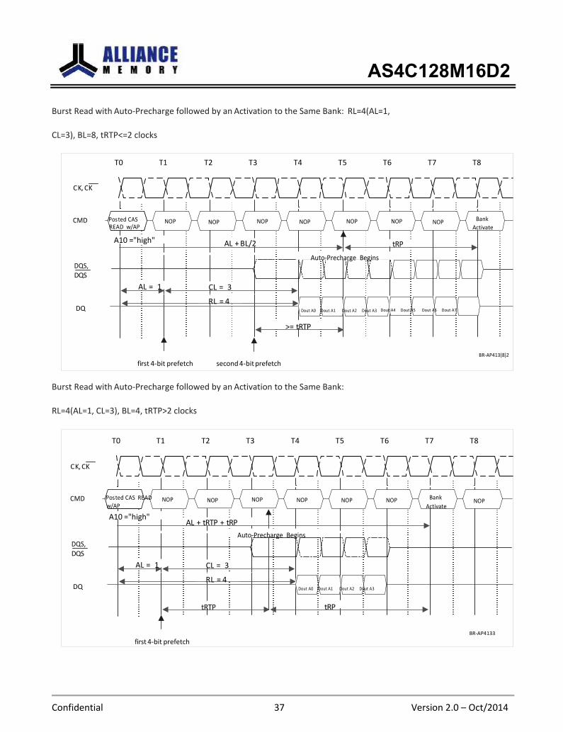
Burst Read with Auto-Precharge followed by an Activation to the Same Bank: RL=4(AL=1,
CL=3), BL=8, tRTP<=2 clocks
T0 T1 T2 T3 T4 T5 T6 T7 T8
CK, CK
CMD Pos ted CAS READ w/AP
A10 ="high"
NOP
NOP
NOP
AL + BL/2
NOP
NOP NOP
tRP
NOP Bank
Activate
DQS,
DQS
DQ
AL = 1 CL = 3
RL = 4
Auto-Precharge Begins
Dout A0 Dout A1 Dout A2 Dout A3 Dout A4 Dout A5 Dout A6 Dout A7
>= tRTP
firs t 4-bit prefetch second 4-bit prefetch BR-AP413(8)2
Burst Read with Auto-Precharge followed by an Activation to the Same Bank:
RL=4(AL=1, CL=3), BL=4, tRTP>2 clocks
T0 T1 T2 T3 T4 T5 T6 T7 T8
CK, CK
CMD Pos ted CAS READ
w/AP
A10 ="high"
NOP
NOP
AL + tRTP + tRP
NOP
NOP NOP NOP Bank
Activate
NOP
DQS,
DQS
DQ
AL = 1 CL = 3
RL = 4
Auto-Precharge Begins
Dout A0 Dout A1 Dout A2 Dout A3
tRTP tRP
firs t 4-bit prefetch BR-AP4133

AS4C128M16D2
Confidential 38 Version 2.0 – Oct/2014
B urst Write with A uto-Precharge
If A10 is high when a Write Command is issued, the Write with Auto-Precharge function is engaged. The DDR2
SDRAM automatically begins precharge operation after the completion of the write burst plus the write recovery
time delay (WR), programmed in the MRS regis ter, as long as tRAS is satisfied. The bank undergoing Auto-Precharge
from the completion of the write burst may be reactivated if the following two conditions are satisfied.
(1) The las t data-in to bank activate delay time (tDAL = WR + tRP) has been satisfied.
(2) The RAS cycle time (tRC) from the previous bank activation has been satisfied.
In DDR2 SDRAMs the write recovery time delay (WR ) has to be programmed into the MRS mode regis ter. As long as
the analog tWR timing parameter is not violated, WR can be programmed between 2 and 6 clock cycles. Minimum
Write to Activate command spacing to the same bank = WL + B L /2 + tDAL.
E xamples:
B urs t Write wi th A uto-Prec harge (tRC L imi t) : WL = 2, tDAL = 6 (WR = 3, tRP = 3) , B L = 4
T0 T1 T2 T3 T4 T5 T6 T7
CK, CK
CMD
WR ITE A
NOP
NOP
NOP
NOP NOP NOP NOP Bank A
Activate
DQS,
DQS
A10 ="high"
C ompletion of the Burst W rite
Auto-Precharge Begins
WL = RL-1 = 2 WR
tDAL
tRP
DQ DIN A0 DIN A1 DIN A2 DIN A3
tRCmin.
>=tRAS min.
BW -AP223
AS4C128M16D2
Confidential 39 Version 2.0 – Oct/2014
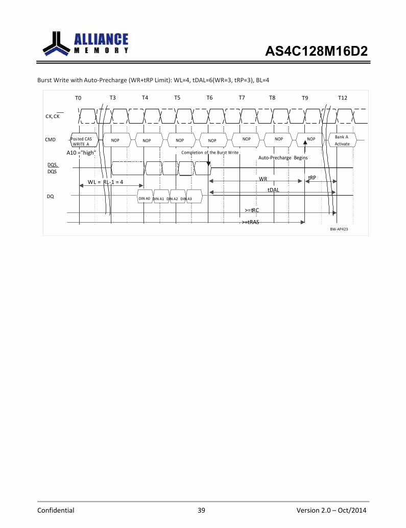
Burst Write with Auto-Precharge (WR+tRP Limit): WL=4, tDAL=6(WR=3, tRP=3), BL=4
T0 T3 T4 T5 T6 T7 T8 T9 T12
CK, CK
CMD Pos ted CAS WR ITE A
NOP
NOP
NOP
NOP NOP NOP NOP Bank A
Activate
DQS,
DQS
A10 ="high" C ompletion of the Burst W rite Auto-Precharge Begins
WL = RL-1 = 4
DQ
DIN A0 DIN A1 DIN A2 DIN A3
WR
>=tRC
>=tRAS
tDAL
tRP
BW -AP423
AS4C128M16D2
Confidential 40 Version 2.0 – Oct/2014
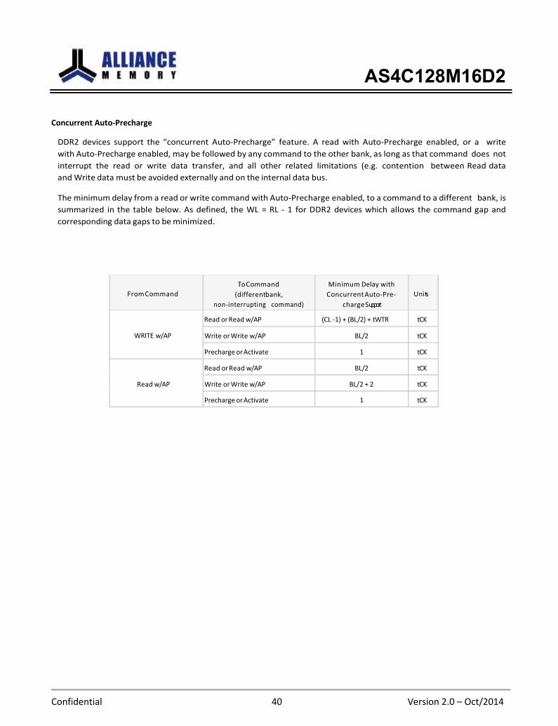
Concurrent Auto-Precharge
DDR2 devices support the “concurrent Auto-Precharge” feature. A read with Auto-Precharge enabled, or a write
with Auto-Precharge enabled, may be followed by any command to the other bank, as long as that command does not
interrupt the read or write data transfer, and all other related limitations (e.g. contention between Read data
and Write data must be avoided externally and on the internal data bus.
The minimum delay from a read or write command with Auto-Precharge enabled, to a command to a different bank, is
summarized in the table below. As defined, the WL = RL - 1 for DDR2 devices which allows the command gap and
corresponding data gaps to be minimized.
From Command
To Command
(different bank,
non-interrupting command)
Minimum Delay wi th
Concurrent Auto-Pre-
charge Support
Units
WRITE w/AP
Read or Read w/AP (CL -1) + (BL /2) + tWTR tCK
Write or Write w/AP BL /2 tCK
Precharge or Activate 1 tCK
Read w/AP
Read or Read w/AP BL /2 tCK
Write or Write w/AP BL/2 + 2 tCK
Precharge or Activate 1 tCK
AS4C128M16D2
Confidential 41 Version 2.0 – Oct/2014
Refresh
SDRAMs require a refresh of all rows in any rolling 64 ms interval. Each refresh is generated in one of two ways : by
an explicit Auto-Refresh command, or by an internally timed event in Self-Refresh mode. Dividing the number of
device rows into the rolling 64 ms interval defined the average refresh interval tREFI, which is a guideline to
controllers for distributed refresh timing. For example, a 512Mbit DDR2 SDRAM has 8192 rows resulting in a tREFI of
7,8 µs.
Auto-Refresh Command
Auto-Refresh is used during normal operation of the DDR2 SDRAMs. This command is non-persistent, so it must be
issued each time a refresh is required. The refresh addressing is generated by the internal refresh controller. This
makes the address bits ”Don’t Care” during an Auto-Refresh command. The DDR2 SDRAM requires Auto-Refresh
cycles at an average periodic interval of tREFI (maximum).
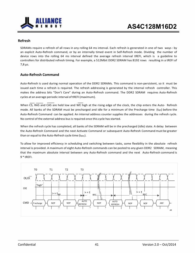
When CS, RAS and CAS are held low and WE high at the rising edge of the clock, the chip enters the Auto- Refresh
mode. All banks of the SDRAM must be precharged and idle for a minimum of the Precharge time (tRP) before the
Auto-Refresh Command can be applied. An internal address counter supplies the addresses during the refresh cycle.
No control of the external address bus is required once this cycle has started.
When the refresh cycle has completed, all banks of the SDRAM will be in the precharged (idle) state. A delay between
the Auto-Refresh Command and the next Activate Command or subsequent Auto-Refresh Command must be greater
than or equal to the Auto-Refresh cycle time (tRFC).
To allow for improved efficiency in scheduling and switching between tasks, some flexibility in the absolute refresh
interval is provided. A maximum of eight Auto-Refresh commands can be posted to any given DDR2 SDRAM, meaning
that the maximum absolute interval between any Auto-Refresh command and the next Auto-Refresh command is
9 * tREFI.
T0 T1 T2 T3
CK, CK
CKE
"high"
> = tRP
> = t RFC
> = t RFC
CMD P recharge
NOP
AUTO NOP REFRESH
NOP
AUTO
REFRESH
NOP NOP
ANY
AR
AS4C128M16D2
Confidential 42 Version 2.0 – Oct/2014
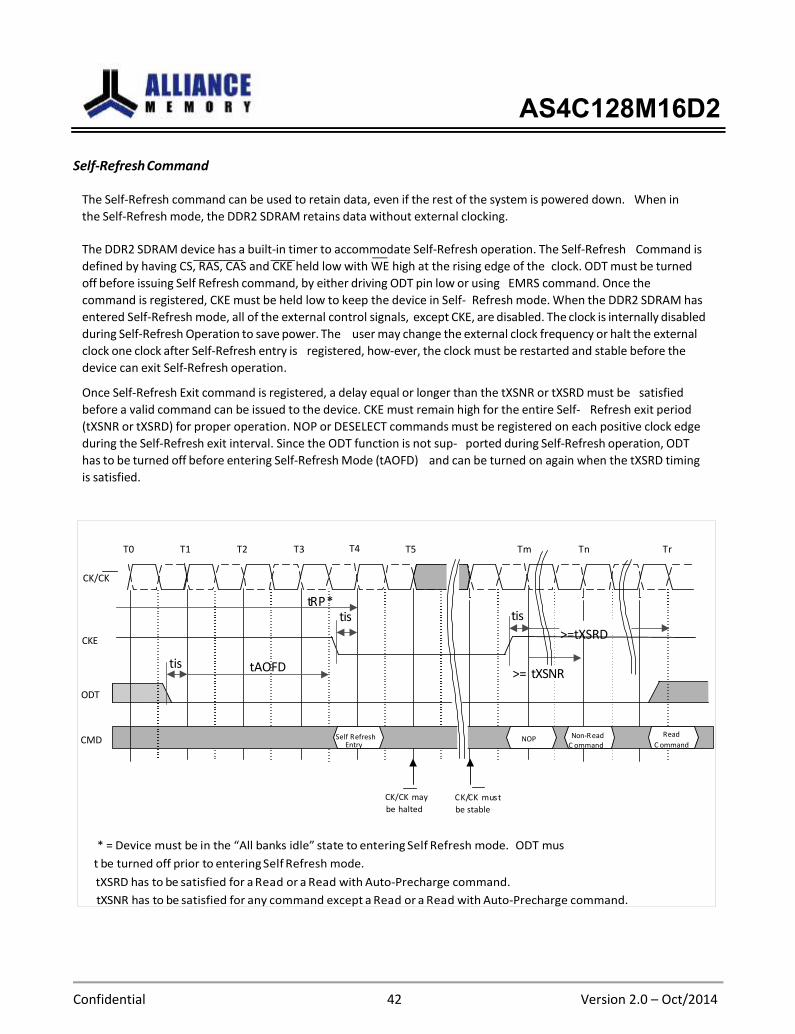
Self-Refresh Command
The Self-Refresh command can be used to retain data, even if the rest of the system is powered down. When in
the Self-Refresh mode, the DDR2 SDRAM retains data without external clocking.
The DDR2 SDRAM device has a built-in timer to accommodate Self-Refresh operation. The Self-Refresh Command is
defined by having CS, RAS, CAS and CKE held low with WE high at the rising edge of the clock. ODT must be turned
off before issuing Self Refresh command, by either driving ODT pin low or using EMRS command. Once the
command is registered, CKE must be held low to keep the device in Self- Refresh mode. When the DDR2 SDRAM has
entered Self-Refresh mode, all of the external control signals, except CKE, are disabled. The clock is internally disabled
during Self-Refresh Operation to save power. The user may change the external clock frequency or halt the external
clock one clock after Self-Refresh entry is registered, how-ever, the clock must be restarted and stable before the
device can exit Self-Refresh operation.
Once Self-Refresh Exit command is registered, a delay equal or longer than the tXSNR or tXSRD must be satisfied
before a valid command can be issued to the device. CKE must remain high for the entire Self- Refresh exit period
(tXSNR or tXSRD) for proper operation. NOP or DESELECT commands must be registered on each positive clock edge
during the Self-Refresh exit interval. Since the ODT function is not sup- ported during Self-Refresh operation, ODT
has to be turned off before entering Self-Refresh Mode (tAOFD) and can be turned on again when the tXSRD timing
is satisfied.
T0 T1 T2 T3 T4 T5 Tm Tn Tr
CK/CK
tRP*
tis
tis
CKE >=tXSRD
ODT
tis tAOFD
>= tXSNR
CMD Self R efresh Entry
NOP Non-R ead C ommand
R ead
C ommand
CK/CK may
be halted
CK/CK must
be stable
* = Device must be in the “All banks idle” sta te to entering Self Refresh mode. ODT mus
t be turned off prior to entering Self R efresh mode.
tXSRD has to be satisfied for a Read or a Read with Auto-Precharge command.
tXSNR has to be satisfied for any command except a Read or a Read with Auto-Precharge command.
AS4C128M16D2
Confidential 43 Version 2.0 – Oct/2014
Power-Down
Power-down is synchronously entered when CKE is registered low along with NOP or Deselect command. No read
or write operation may be in progress when CKE goes low. These operations are any of the following: read burst or
write burst and recovery. CKE is allowed to go low while any of other operations such as row activation, precharge
or autoprecharge, mode register or extended mode register command time, or auto refresh is in progress. The DLL
should be in a locked state when power-down is entered. Otherwise DLL should be reset after exiting power-down
mode for proper read operation.
If power-down occurs when all banks are precharged, this mode is referred to as Precharge Power-down; if power-
down occurs when there is a row active in any bank, this mode is referred to as Active Power-down. For Active
Power-down two different power saving modes can be selected within the MRS register, address bit A12. When A12
is set to “low” this mode is referred as “standard active power-down mode” and a fast power-down exit timing
defined by the tXARD timing parameter can be used. When A12 is set to “high” this mode is referred as a power
saving “low power active power-down mode”. This mode takes longer to exit from the power-down mode and the
tXARDS timing parameter has to be satisfied.
Entering power-down deactivates the input and output buffers, excluding CK, CK, ODT and CKE. Also the DLL is
disabled upon entering precharge power-down or slow exit active power-down, but the DLL is kept enabled during
fast exit active power-down. In power-down mode, CKE low and a stable clock signal must be maintained at the inputs
of the DDR2 SDRAM, and all other input signals are “Don’t Care”. Power-down duration is limited by 9 times tREFI of the
device.
The power-down state is synchronously exited when CKE is registered high (along with a NOP or Deselect
command). A valid, executable command can be applied with power-down exit latency, tsp., tXARD or tXARDS,
after CKE goes high. Power-down exit latencies are defined in the AC spec table of this data sheet.
Power-Down Entry
Active Power-down mode can be entered after an activate command. Precharge Power-down mode can be entered
after a precharge, precharge-all or internal precharge command. It is also allowed to enter power- mode after an
Auto-Refresh command or MRS / EMRS command when timed is satisfied.
Active Power-down mode entry is prohibited as long as a Read Burst is in progress, meaning CKE should be kept high
until the burst operation is finished. Therefore Active Power-Down mode entry after a Read or Read with Auto-
Precharge command is allowed after RL + BL/2 is satisfied.
Active Power-down mode entry is prohibited as long as a Write Burst and the internal write recovery is in
progress. In case of a write command, active power-down mode entry is allowed when WL + BL/2 + tWTR is satisfied.
In case of a write command with auto-precharge, power-down mode entry is allowed after the internal pre- charge
command has been executed, which WL + BL/2 + WR is starting from the write with auto-precharge command. In case
the DDR2 SDRAM enters the Precharge Power-down mode.
AS4C128M16D2
Confidential 44 Version 2.0 – Oct/2014
NOP
OP
T8
NO
NOP
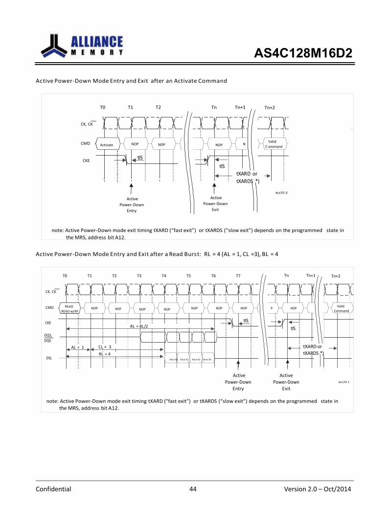
Ac tive Power-Down Mode E n try and E xi t after an Activate Command
T0 T1 T2 Tn Tn+1 Tn+2
CK, CK
CMD
CKE
Activate
NOP NOP
tIS
NOP
tIS
N
tXAR D or
tXAR DS *)
Valid
C ommand
Active
Power-Down
Entry
Active
Power-Down
Exit
Act.PD 0
note: Active Power-Down mode exit timing tXARD (“fast exit”) or tXARDS (“slow exit”) depends on the programmed state in
the MRS, address bit A12.
Active Power-Down Mode E n try and E xi t after a Read B urs t: RL = 4 (AL = 1, CL =3), BL = 4
T0 T1 T2 T3 T4 T5 T6 T7 Tn Tn+1 Tn+2
CK, CK
CMD
CKE
DQS,
DQS
READ
READ w/AP
AL = 1
NOP NOP
CL = 3
RL = 4
NOP NOP
RL + BL /2
NOP NOP NOP P NOP
tIS
tIS
tXARD or
tXARDS *)
Valid
C ommand
DQ Dout A0 Dout A1 Dout A2 Dout A3
Active
Power-Down
Entry
Active
Power-Down
Exit
Act.PD 1
note: Active Power-Down mode exit timing tXARD (“fast exit”) or tXARDS (“slow exit”) depends on the programmed state in
the MRS, address bit A12.
AS4C128M16D2
Confidential 45 Version 2.0 – Oct/2014
NO
NOP
OP
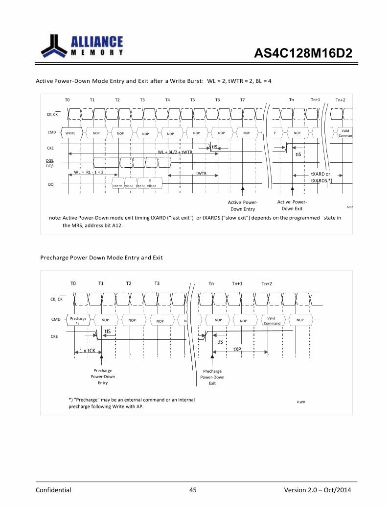
Acti v e Power -Down Mode Entry a nd Exit after a Write Bu rst: WL = 2, tWTR = 2, BL = 4
T0 T1 T2 T3 T4 T5 T6 T7 Tn Tn+1 Tn+2
CK, CK
CMD
WRITE
NOP NOP
NOP NOP
NOP NOP NOP P NOP
Valid
Comman
CKE
DQS,
DQS
DQ
WL = RL - 1 = 2
WL + BL/2 + tWTR
tWTR
Dout A0 Dout A1 Dout A2 Dout A3
tIS
tIS
tXARD or
tXARDS *)
Active Power-
Down Entry
Active Power-
Down Exit
Act.P
note: Active Power-Down mode exit timing tXARD (“fast exit”) or tXARDS (“slow exit”) depends on the programmed state in
the MRS, address bit A12.
Precharge Power Down Mode Entry and Exit
T0 T1 T2 T3 Tn Tn+1 Tn+2
CK, CK
CMD
CKE
Precharge
*)
1 x tCK
NOP NOP
tIS
NOP N
NOP
tIS
NOP
tXP
Valid
Command
NOP
Precharge
Power-Down
Entry
Precharge
Power-Down
Exit
*) "Precharge" may be an external command or an internal
precharge following Write with AP.
PrePD
AS4C128M16D2
Confidential 46 Version 2.0 – Oct/2014
No Operation Command
The No Operation Command should be used in cases when the SDRAM is in an idle or a wait state. The purpose of the
No Operation Command is to prevent the SDRAM from registering any unwanted commands between operations.
A No Operation Command is registered when CS is low with RAS, CAS, and WE held high at the rising edge of the
clock. A No Operation Command will not terminate a previous operation that is still executing, such as a burst read or
write cycle.
Deselect Command
The Deselect Command performs the same function as a No Operation Command. Deselect Command occurs when CS is
brought high, the RAS, CAS, and WE signals become don’t care.
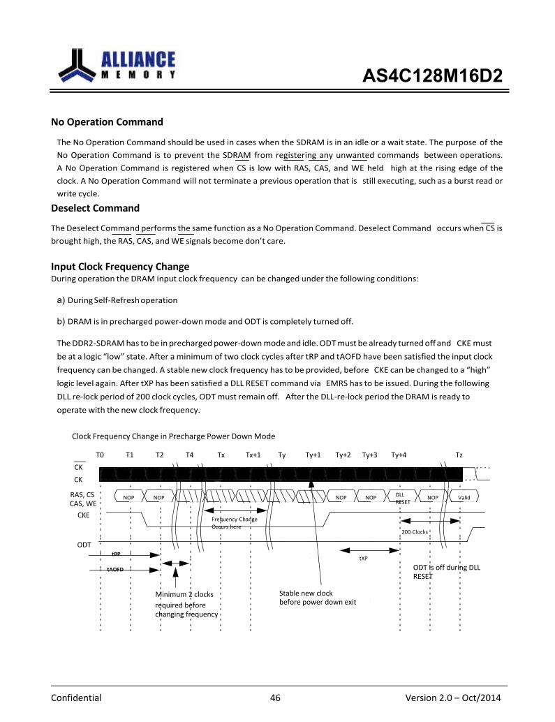
Input Clock Frequency Change During operation the DRAM input clock frequency can be changed under the following conditions:
a) During Self-Refresh operation
b) DRAM is in precharged power-down mode and ODT is completely turned off.
The DDR2-SDRAM has to be in precharged power-down mode and idle. ODT must be already turned off and CKE must
be at a logic “low” state. After a minimum of two clock cycles after tRP and tAOFD have been satisfied the input clock
frequency can be changed. A stable new clock frequency has to be provided, before CKE can be changed to a “high”
logic level again. After tXP has been satisfied a DLL RESET command via EMRS has to be issued. During the following
DLL re-lock period of 200 clock cycles, ODT must remain off. After the DLL-re-lock period the DRAM is ready to
operate with the new clock frequency.
Clock Frequency Change in Precharge Power Down Mode
T0 T1 T2 T4
CK
CK
Tx Tx+1 Ty Ty+1 Ty+2 Ty+3 Ty+4 Tz
RAS, CS CAS, WE
CKE
NOP
NOP NOP NOP
Frequency Change Occurs here
DLL RESET
NOP
Valid
ODT
tRP
tAOFD
Minimum 2 clocks
Stable new clock
tXP
200 Clocks
ODT is off during DLL RESET
required before changing frequency
before power down exit
AS4C128M16D2
Confidential 47 Version 2.0 – Oct/2014
Asynchronous CKE Low Event
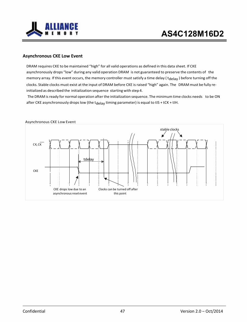
DRAM requires CKE to be maintained “high” for all valid operations as defined in this data sheet. If CKE
asynchronously drops “low” during any valid operation DRAM is not guaranteed to preserve the contents of the
memory array. If this event occurs, the memory controller must satisfy a time delay ( tdelay ) before turning off the
clocks. Stable clocks must exist at the input of DRAM before CKE is raised “high” again. The DRAM must be fully re-
initialized as described the initialization sequence starting with step 4.
The DRAM is ready for normal operation after the initialization sequence. The minimum time clocks needs to be ON
after CKE asynchronously drops low (the tdelay timing parameter) is equal to tIS + tCK + tIH.
Asynchronous CKE L ow E ven t
stable clocks
CK, CK
tdelay
CKE
CKE drops low due to an
asynchronous reset event
Clocks can be turned off after
this point

AS4C128M16D2
Confidential 48 Version 2.0 – Oct/2014
Command Truth Table
Function
CKE
CS
RAS
CAS
WE
BA0
-
BAx9
Axx9-A11
A10
A9 - A0
Notes
Previous
Cycle
Current
Cycle
(Extended) Mode Register Set
H
H
L
L
L
L
BA
OP Code
1,2
Refresh (REF) H H L L L H X X X X 1
Self Refresh Entry H L L L L H X X X X 1,8
Self Refresh Exit
L
H H X X X
X
X
X
X
1,7,8 L H H H
Single Bank Precharge H H L L H L BA X L X 1,2
Precharge all Banks H H L L H L X X H X 1
Bank Activate H H L L H H BA Row Address 1,2
Write H H L H L L BA Column L Column 1,2,3,
Write with Auto Precharge H H L H L L BA Column H Column 1,2,3,
Read H H L H L H BA Column L Column 1,2,3
Read with Auto-Precharge H H L H L H BA Column H Column 1,2,3
No Operation H X L H H H X X X X 1
Device Deselect H X H X X X X X X X 1
Power Down Entry
H
L H X X X
X
X
X
X
1,4 L H H H
Power Down Exit
L
H H X X X
X
X
X
X
1,4 L H H H
NOTE 1 All DDR2 SDRAM commands are defined by states of CS, RAS, CAS , WE and CKE at the rising edge of the clock. NOTE 2
Bank addresses BA0, BA1, BA2 (BA) determine which bank is to be operated upon. For (E)MRS BA selects an (Extended) Mode
Register.
NOTE 3 Burst reads or writes at BL=4 cannot be terminated or interrupted. See sections "Reads interrupted by a Read" and
"Writes interrupted by a Write" in section 2.6 for details.
NOTE 4 The Power Down Mode does not perform any refresh operations. The duration of Power Down is therefore limited by the
refresh requirements outlined in section 2.9.
NOTE 5 The state of ODT does not affect the states described in this table. The ODT function is not available during Self Refresh.
See section 2.4.4.
NOTE 6 “X” means “H or L (but a defined logic level)” NOTE 7
Self refresh exit is asynchronous.
NOTE 8 VREF must be maintained during Self Refresh operation.
NOTE 9 BAx and Axx refers to the MSBs of bank addresses and addresses, respectively, per device density.

AS4C128M16D2
Confidential 49 Version 2.0 – Oct/2014
Clock enable (CKE) truth table for synchronous transitions
Current State 2
CKE Command (N) 3
RAS, CAS, WE, CS
Action (N) 3
Notes Previous Cycle 1
(N-1)
Current Cycle 1
(N)
Power Down
L L X Maintain Power-Down 11, 13, 14
L H DESELECT or NOP Power Down Exit 4, 8, 11,13
Self Refresh
L L X Maintain Self Refresh 11, 14,15
L H DESELECT or NOP Self Refresh Exit 4, 5, 9, 15
Bank(s) Active H L DESELECT or NOP Active Power Down Entry 4, 8, 10, 11, 13
All Banks Idle
H L DESELECT or NOP Precharge Power Down Entry 4, 8, 10, 11,13
H L REFRESH Self Refresh Entry 6, 9, 11,13
H H Refer to the Command Truth Table 7
NOTE 1 CKE (N) is the logic state of CKE at clock edge N; CKE (N–1) was the state of CKE at the previous clock edge. NOTE 2
Current state is the state of the DDR2 SDRAM immediately prior to clock edge N.
NOTE 3 COMMAND (N) is the command registered at clock edge N, and ACTION (N) is a result of COMMAND (N). NOTE 4
All states and sequences not shown are illegal or reserved unless explicitly described elsewhere in this document.
NOTE 5 On Self Refresh Exit DESELECT or NOP commands must be issued on every clock edge occurring during the tXSNR
period. Read commands may be issued only after tXSRD (200 clocks) is satisfied.
NOTE 6 Self Refresh mode can only be entered from the All Banks Idle state. NOTE
7 Must be a legal command as defined in the Command Truth Table.
NOTE 8 Valid commands for Power Down Entry and Exit are NOP and DESELECT only. NOTE 9
Valid commands for Self Refresh Exit are NOP and DESELECT only.
NOTE 10 Power Down and Self Refresh cannot be entered while Read or Write operations, (Extended) Mode Register Set operations or Precharge operations are in progress. See section Power-down and Self refresh operation for a detailed list of restrictions.
NOTE 11 tCKEmin of 3 clocks means CKE must be registered on three consecutive positive clock edges. CKE must remain at the
valid input level the entire time it takes to achieve the 3 clocks of registration. Thus, after any CKE transition, CKE may
not transition from its valid level during the time period of tIS + 2 x tCK + tIH.
NOTE 12 The state of ODT does not affect the states described in this table. The ODT function is not available during Self
Refresh.
NOTE 13 The Power Down does not perform any refresh operations. The duration of Power Down Mode is therefore limited by
the refresh requirements outlined in Refresh command section.
NOTE 14 “X” means “don’t care (including floating around VREF)” in Self Refresh and Power Down. However ODT must be
driven HIGH or LOW in Power Down if the ODT function is enabled (Bit A2 or A6 set to “1” in EMR(1) ).
NOTE 15 VREF must be maintained during Self Refresh operation.
AS4C128M16D2
Confidential 50 Version 2.0 – Oct/2014
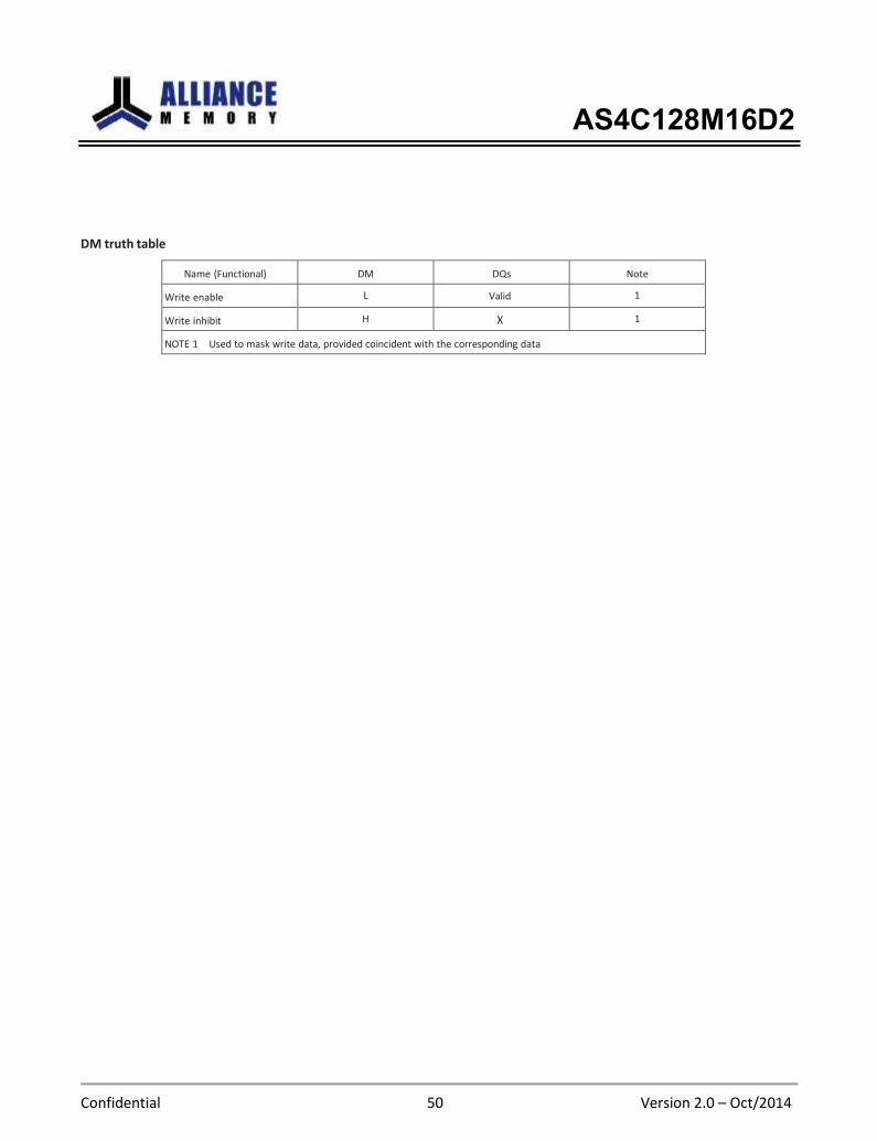
DM truth table
Name (Functional) DM DQs Note
Write enable L Valid 1
Write inhibit H X 1
NOTE 1 Used to mask write data, provided coincident with the corresponding data
AS4C128M16D2
Confidential 51 Version 2.0 – Oct/2014
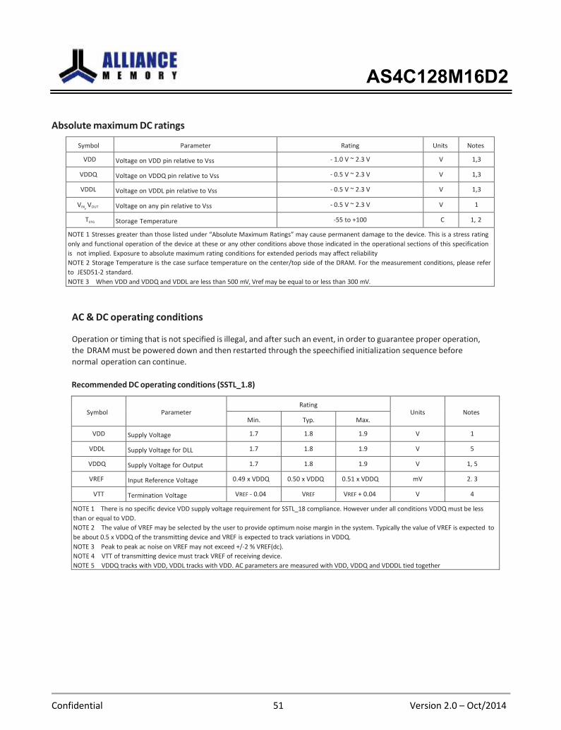
Absolute maximum DC ratings
Symbol Parameter Rating Units Notes
VDD Voltage on VDD pin relative to Vss - 1.0 V ~ 2.3 V V 1,3
VDDQ Voltage on VDDQ pin relative to Vss - 0.5 V ~ 2.3 V V 1,3
VDDL Voltage on VDDL pin relative to Vss - 0.5 V ~ 2.3 V V 1,3
VIN, VOUT Voltage on any pin relative to Vss - 0.5 V ~ 2.3 V V 1
TSTG Storage Temperature -55 to +100 C 1, 2
NOTE 1 Stresses greater than those listed under “Absolute Maximum Ratings” may cause permanent damage to the device. This is a stress rating
only and functional operation of the device at these or any other conditions above those indicated in the operational sections of this specification
is not implied. Exposure to absolute maximum rating conditions for extended periods may affect reliability
NOTE 2 Storage Temperature is the case surface temperature on the center/top side of the DRAM. For the measurement conditions, please refer
to JESD51-2 standard.
NOTE 3 When VDD and VDDQ and VDDL are less than 500 mV, Vref may be equal to or less than 300 mV.
AC & DC operating conditions
Operation or timing that is not specified is illegal, and after such an event, in order to guarantee proper operation,
the DRAM must be powered down and then restarted through the speechified initialization sequence before
normal operation can continue.
Recommended DC operating conditions (SSTL_1.8)
Symbol
Parameter
Rating
Units
Notes
Min. Typ. Max.
VDD Supply Voltage 1.7 1.8 1.9 V 1
VDDL Supply Voltage for DLL 1.7 1.8 1.9 V 5
VDDQ Supply Voltage for Output 1.7 1.8 1.9 V 1, 5
VREF Input Reference Voltage 0.49 x VDDQ 0.50 x VDDQ 0.51 x VDDQ mV 2. 3
VTT Termination Voltage VREF - 0.04 VREF VREF + 0.04 V 4
NOTE 1 There is no specific device VDD supply voltage requirement for SSTL_18 compliance. However under all conditions VDDQ must be less
than or equal to VDD.
NOTE 2 The value of VREF may be selected by the user to provide optimum noise margin in the system. Typically the value of VREF is expected to
be about 0.5 x VDDQ of the transmitting device and VREF is expected to track variations in VDDQ.
NOTE 3 Peak to peak ac noise on VREF may not exceed +/-2 % VREF(dc).
NOTE 4 VTT of transmitting device must track VREF of receiving device.
NOTE 5 VDDQ tracks with VDD, VDDL tracks with VDD. AC parameters are measured with VDD, VDDQ and VDDDL tied together
AS4C128M16D2
Confidential 52 Version 2.0 – Oct/2014
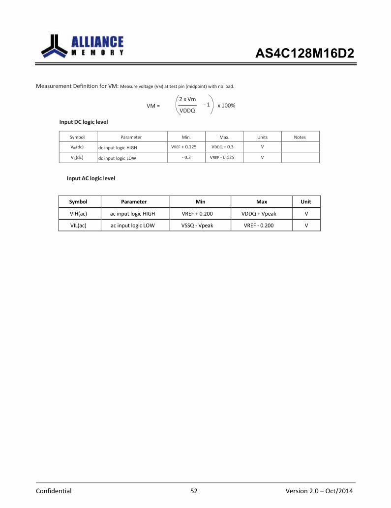
Measurement Definition for VM: Measure voltage (VM) at test pin (midpoint) with no load.
Input DC logic level
VM =
2 x Vm - 1
VDDQ
x 100%
Symbol Parameter Min. Max. Units Notes
VIH(dc) dc input logic HIGH VREF + 0.125 VDDQ + 0.3 V
VIL(dc) dc input logic LOW - 0.3 VREF - 0.125 V
Input AC logic level
Symbol Parameter Min Max Unit
VIH(ac) ac input logic HIGH VREF + 0.200 VDDQ + Vpeak V
VIL(ac) ac input logic LOW VSSQ - Vpeak VREF - 0.200 V
AS4C128M16D2
Confidential 53 Version 2.0 – Oct/2014
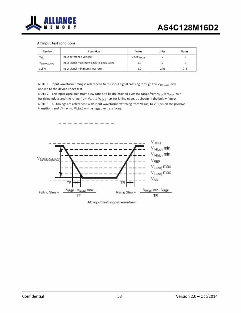
AC input test conditions
Symbol Condition Value Units Notes
VREF Input reference voltage 0.5 x VDDQ V 1
VSWING(MAX) Input signal maximum peak to peak swing 1.0 V 1
SLEW Input signal minimum slew rate 1.0 V/ns 2, 3
NOTE 1 Input waveform timing is referenced to the input signal crossing through the VIH/IL(AC) level
applied to the device under test.
NOTE 2 The input signal minimum slew rate is to be maintained over the range from VREF to VIH(ac) min
for rising edges and the range from VREF to VIL(ac) max for falling edges as shown in the below figure.
NOTE 3 AC timings are referenced with input waveforms switching from VIL(ac) to VIH(ac) on the positive
transitions and VIH(ac) to VIL(ac) on the negative transitions.
AS4C128M16D2
Confidential 54 Version 2.0 – Oct/2014
Symbol Parameter Min. Max. Units Notes
VID (ac) ac differential input voltage 0.5 VDDQ V 1
VIX (ac) ac differential cross point voltage 0.5 x VDDQ - 0.175 0.5 x VDDQ + 0.175 V 2
AC & DC operating conditions (cont'd)
Differential input AC logic level
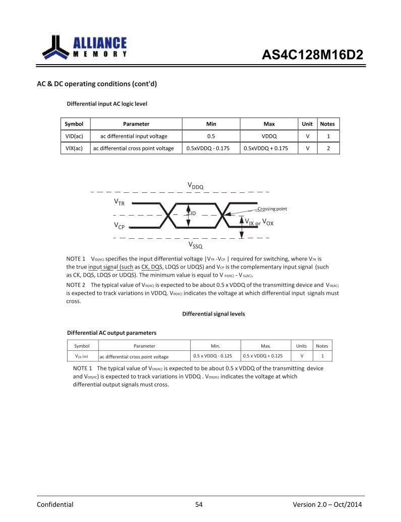
Symbol Parameter Min Max Unit Notes
VID(ac) ac differential input voltage 0.5 VDDQ V 1
VIX(ac) ac differential cross point voltage 0.5xVDDQ - 0.175 0.5xVDDQ + 0.175 V 2
VTR
VCP
VDDQ
VID
VSSQ
Crossing point
VIX or VOX
NOTE 1 VID(AC) specifies the input differential voltage |VTR -VCP | required for switching, where VTR is
the true input signal (such as CK, DQS, LDQS or UDQS) and VCP is the complementary input signal (such
as CK, DQS, LDQS or UDQS). The minimum value is equal to V IH(AC) - V IL(AC).
NOTE 2 The typical value of VIX(AC) is expected to be about 0.5 x VDDQ of the transmitting device and VIX(AC)
is expected to track variations in VDDQ. VIX(AC) indicates the voltage at which differential input signals must
cross.
Differential signal levels
Dif ferential AC output parameters
Symbol Parameter Min. Max. Units Notes
VOX (ac) ac differential cross point voltage 0.5 x VDDQ - 0.125 0.5 x VDDQ + 0.125 V 1
NOTE 1 The typical value of VOX(AC) is expected to be about 0.5 x VDDQ of the transmitting device
and VOX(AC) is expected to track variations in VDDQ . VOX(AC) indicates the voltage at which
differential output signals must cross.
AS4C128M16D2
Confidential 55 Version 2.0 – Oct/2014
Parameter Specification
DDR2-667 DDR2-800
Maximum peak amplitude allowed for overshoot area (See Figure 74): 0.5(0.9)1 V 0.5(0.9)1 V
Maximum peak amplitude allowed for undershoot area (See Figure 74): 0.5(0.9)1 V 0.5(0.9)1 V
Maximum overshoot area above VDD (See Figure 74). 0.8 V-ns 0.66 V-ns
Maximum undershoot area below VSS (See Figure 74). 0.8 V-ns 0.66 V-ns
Overshoot/undershoot specification
AC overshoot/undershoot specification for address and control pins:
A0-A15, BA0-BA2, CS, RAS, CAS, WE, CKE, ODT
Parameter DDR2-800 Unit
Maximum peak amplitude allowed for overshoot area 0.5(0.9)1 V
Maximum peak amplitude allowed for undershoot area 0.5(0.9)1 V
Maximum overshoot area above VDDQ 0.66 V-ns
Maximum undershoot area below VSSQ 0.66 V-ns
NOTE 1 The maximum requirements for peak amplitude were reduced from 0.9V to 0.5V. Register vendor data sheets will specify the
maximum over/undershoot induced in specific RDIMM applications. DRAM vendor data sheets will also specify the maxi- mum
overshoot/undershoot that their DRAM can tolerate. This will allow the RDIMM supplier to understand whether the DRAM can tolerate the
overshoot that the register will induce in the specific RDIMM application.
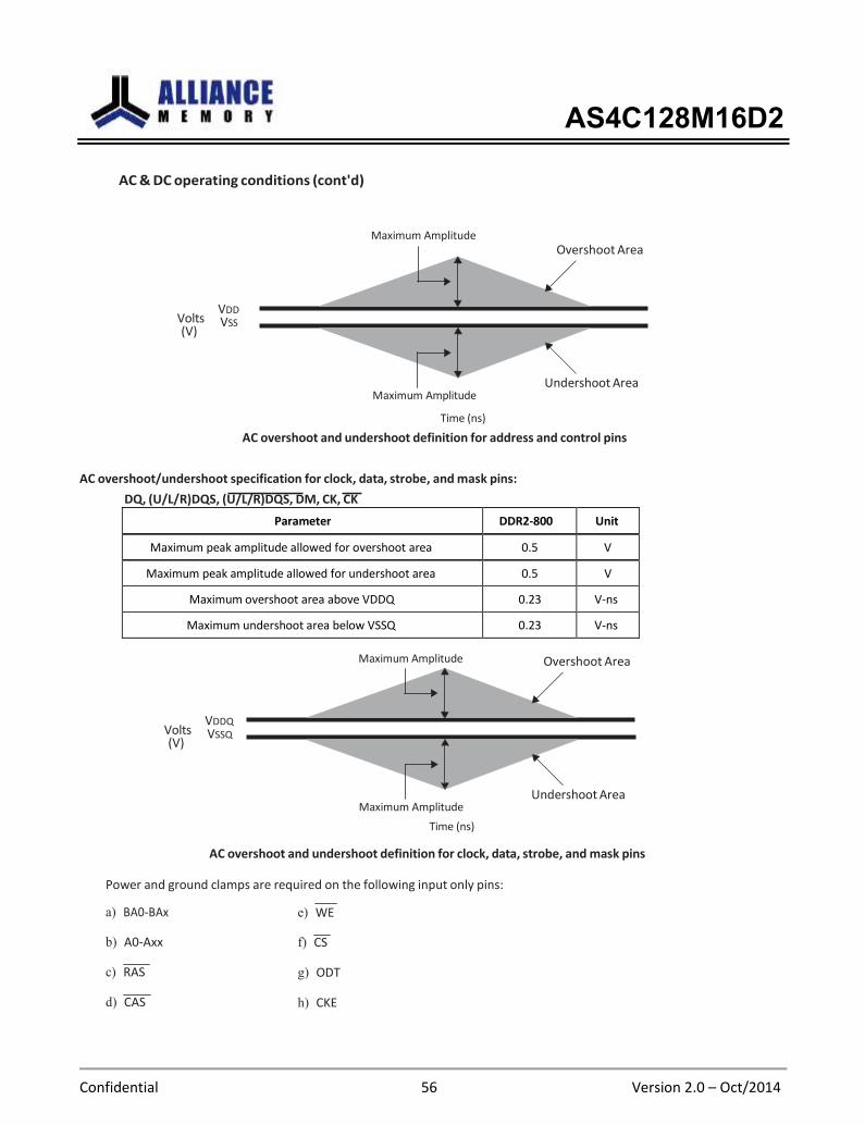
AS4C128M16D2
Confidential 56 Version 2.0 – Oct/2014
Parameter Specification
DDR2-667 DDR2-800
Maximum peak amplitude allowed for overshoot area (See Figure 75): 0.5 V 0.5 V
Maximum peak amplitude allowed for undershoot area (See Figure 75): 0.5 V 0.5 V
Maximum overshoot area above VDDQ (See Figure 75). 0.23 V-ns 0.23 V-ns
Maximum undershoot area below VSSQ (See Figure 75). 0.23 V-ns 0.23 V-ns
AC & DC operating conditions (cont'd)
Maximum Amplitude Overshoot Area
Volts (V)
VDD VSS
Maximum Amplitude
Time (ns)
Undershoot Area
AC overshoot and undershoot definition for address and control pins
AC overshoot/undershoot specification for clock, data, strobe, and mask pins:
DQ, (U/L/R)DQS, (U/L/R)DQS, DM, CK, CK
Parameter DDR2-800 Unit
Maximum peak amplitude allowed for overshoot area 0.5 V
Maximum peak amplitude allowed for undershoot area 0.5 V
Maximum overshoot area above VDDQ 0.23 V-ns
Maximum undershoot area below VSSQ 0.23 V-ns
Maximum Amplitude Overshoot Area
Volts (V)
VDDQ VSSQ
Maximum Amplitude
Time (ns)
Undershoot Area
AC overshoot and undershoot definition for clock, data, strobe, and mask pins
Power and ground clamps are required on the following input only pins:
a) BA0-BAx
b) A0-Axx
c) RAS
d) CAS
e) WE
f) CS
g) ODT
h) CKE
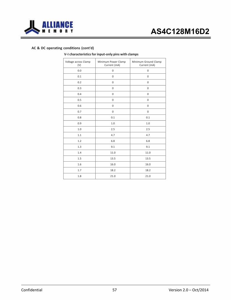
AS4C128M16D2
Confidential 57 Version 2.0 – Oct/2014
AC & DC operating conditions (cont'd)
V-I characteristics for input-only pins with clamps
Voltage across Clamp (V)
Minimum Power Clamp Current (mA)
Minimum Ground Clamp Current (mA)
0.0 0 0
0.1 0 0
0.2 0 0
0.3 0 0
0.4 0 0
0.5 0 0
0.6 0 0
0.7 0 0
0.8 0.1 0.1
0.9 1.0 1.0
1.0 2.5 2.5
1.1 4.7 4.7
1.2 6.8 6.8
1.3 9.1 9.1
1.4 11.0 11.0
1.5 13.5 13.5
1.6 16.0 16.0
1.7 18.2 18.2
1.8 21.0 21.0
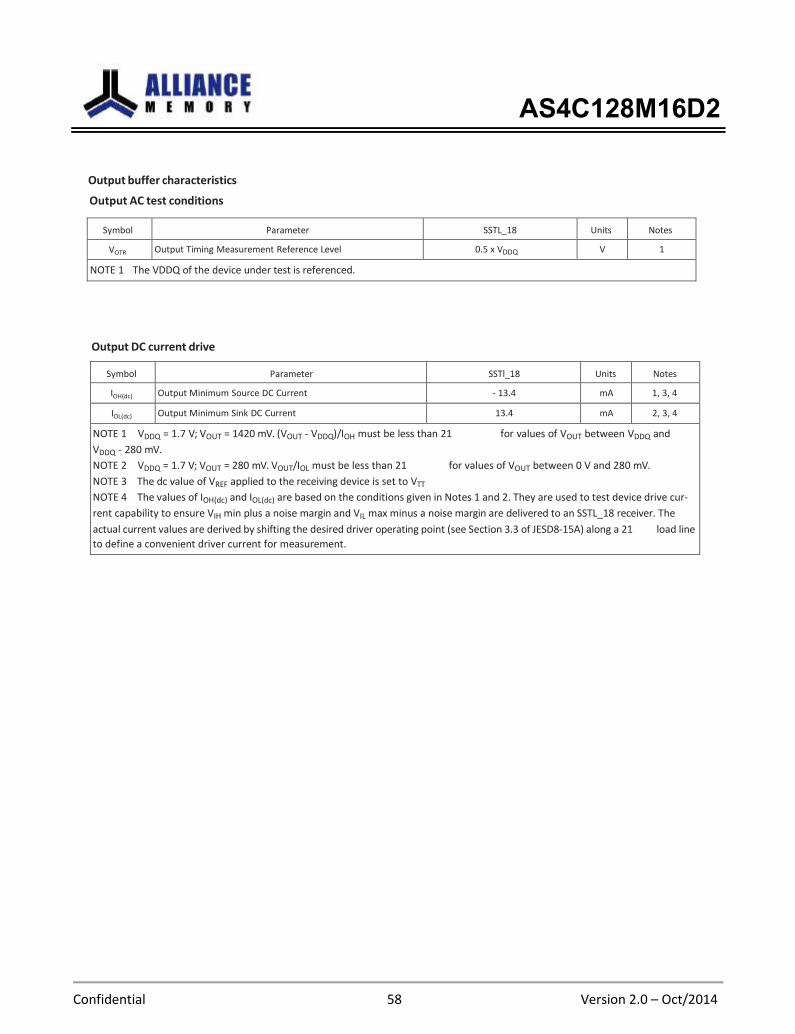
AS4C128M16D2
Confidential 58 Version 2.0 – Oct/2014
Output buffer characteristics
Output AC test conditions
Symbol Parameter SSTL_18 Units Notes
VOTR Output Timing Measurement Reference Level 0.5 x VDDQ V 1
NOTE 1 The VDDQ of the device under test is referenced.
Output DC current drive
Symbol Parameter SSTl_18 Units Notes
IOH(dc) Output Minimum Source DC Current - 13.4 mA 1, 3, 4
IOL(dc) Output Minimum Sink DC Current 13.4 mA 2, 3, 4
NOTE 1 VDDQ = 1.7 V; VOUT = 1420 mV. (VOUT - VDDQ)/IOH must be less than 21 for values of VOUT between VDDQ and
VDDQ - 280 mV.
NOTE 2 VDDQ = 1.7 V; VOUT = 280 mV. VOUT/IOL must be less than 21 for values of VOUT between 0 V and 280 mV.
NOTE 3 The dc value of VREF applied to the receiving device is set to VTT
NOTE 4 The values of IOH(dc) and IOL(dc) are based on the conditions given in Notes 1 and 2. They are used to test device drive cur-
rent capability to ensure VIH min plus a noise margin and VIL max minus a noise margin are delivered to an SSTL_18 receiver. The
actual current values are derived by shifting the desired driver operating point (see Section 3.3 of JESD8-15A) along a 21 load line
to define a convenient driver current for measurement.
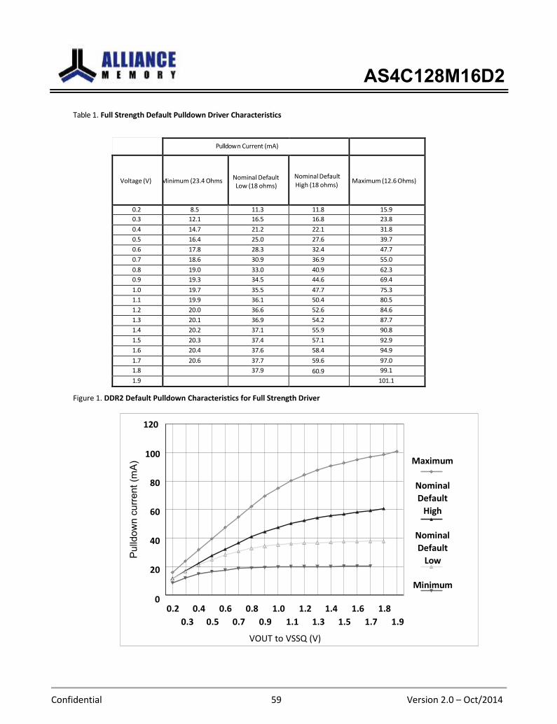
AS4C128M16D2
Confidential 59 Version 2.0 – Oct/2014
Pu
lldo
wn
cu
rre
nt
(mA
)
Table 1. Full Strength Default Pulldown Driver Characteristics
Pulldow n Current (mA)
Voltage (V)
Minimum (23.4 Ohms
) Nominal Default Low (18 ohms)
Nominal Default High (18 ohms)
Maximum (12.6 Ohms)
0.2 8.5 11.3 11.8 15.9
0.3 12.1 16.5 16.8 23.8
0.4 14.7 21.2 22.1 31.8
0.5 16.4 25.0 27.6 39.7
0.6 17.8 28.3 32.4 47.7
0.7 18.6 30.9 36.9 55.0
0.8 19.0 33.0 40.9 62.3
0.9 19.3 34.5 44.6 69.4
1.0 19.7 35.5 47.7 75.3
1.1 19.9 36.1 50.4 80.5
1.2 20.0 36.6 52.6 84.6
1.3 20.1 36.9 54.2 87.7
1.4 20.2 37.1 55.9 90.8
1.5 20.3 37.4 57.1 92.9
1.6 20.4 37.6 58.4 94.9
1.7 20.6 37.7 59.6 97.0
1.8 37.9 60.9 99.1
1.9 101.1
Figure 1. DDR2 Default Pulldown Characteristics for Full Strength Driver
120
100
80
60
40
20
0
0.2
0.4
0.6
0.8
1.0
1.2
1.4
1.6
1.8
Maximum
Nominal
Default
High
Nominal
Default
Low
Minimum
0.3 0.5 0.7 0.9 1.1 1.3 1.5 1.7 1.9
VOUT to VSSQ (V)
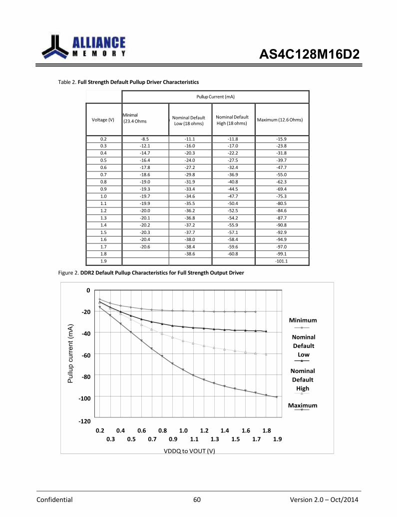
AS4C128M16D2
Confidential 60 Version 2.0 – Oct/2014
Pu
llup
cu
rre
nt
(mA
)
Table 2. Full Strength Default Pullup Driver Characteristics
Pullup Current (mA)
Voltage (V)
Minimal (23.4 Ohms
) Nominal Default
Low (18 ohms)
Nominal Default High (18 ohms)
Maximum (12.6 Ohms)
0.2 -8.5 -11.1 -11.8 -15.9
0.3 -12.1 -16.0 -17.0 -23.8
0.4 -14.7 -20.3 -22.2 -31.8
0.5 -16.4 -24.0 -27.5 -39.7
0.6 -17.8 -27.2 -32.4 -47.7
0.7 -18.6 -29.8 -36.9 -55.0
0.8 -19.0 -31.9 -40.8 -62.3
0.9 -19.3 -33.4 -44.5 -69.4
1.0 -19.7 -34.6 -47.7 -75.3
1.1 -19.9 -35.5 -50.4 -80.5
1.2 -20.0 -36.2 -52.5 -84.6
1.3 -20.1 -36.8 -54.2 -87.7
1.4 -20.2 -37.2 -55.9 -90.8
1.5 -20.3 -37.7 -57.1 -92.9
1.6 -20.4 -38.0 -58.4 -94.9
1.7 -20.6 -38.4 -59.6 -97.0
1.8 -38.6 -60.8 -99.1
1.9 -101.1
Figure 2. DDR2 Default Pullup Characteristics for Full Strength Output Driver
0
-20
-40
-60
Minimum
Nominal
Default
Low
-80
-100
Nominal
Default
High
Maximum
-120
0.2
0.3
0.4
0.5
0.6
0.7
0.8
0.9
1.0
1.1
1.2
1.3
1.4
1.5
1.6
1.7
1.8
1.9
VDDQ to VOUT (V)

AS4C128M16D2
Confidential 61 Version 2.0 – Oct/2014
DDR2 SDRAM Default Output Driver V-I Characteristics
DDR2 SDRAM output driver characteristics are defined for full strength default operation as selected by the EMRS1
bits A7-A9 = '111'. Figures 1 and 2 show the driver characteristics graphically, and tables 1 and 2 show the same data
in tabular format suitable for input into simulation tools. The driver characteristics evaluation conditions are:
Nominal Default 25°C (T case), VDDQ = 1.8V, typical process
Minimum 85°C (T case), VDDQ = 1.7 V, slow - slow process
Maximum 0°C (T case), VDDQ = 1.9V, fast - fast process
Default Output Driver Characteristic Curves Notes:
1) The full variation in driver current from minimum to maximum process, temperature, and voltage will lie within
the outer bounding lines of the V-I curve of figures 1 and 2.
2) It is recommended that the "typical" IBIS V-I curve lie within the inner bounding lines of the V-I curves of
figures 1 and 2.
Table 3. Full Strength Calibrated Pulldown Driver Characteristics
Calibrated Pulldow n Current (mA)
Voltage (V)
Nominal Minimum
(21 ohms)
Nominal Low
(18.75 ohms)
Nominal (18 ohms)
Nominal High
(17.2 ohms)
Nominal Maximum
(15 ohms)
0.2 9.5 10.7 11.5 11.8 13.3
0.3 14.3 16.0 16.6 17.4 20.0
0.4 18.7 21.0 21.6 23.0 27.0
Table 4. Full Strength Calibrated Pullup Driver Characteristics
Calibrated Pullup Current (mA)
Voltage (V)
Nominal Minimum
(21 ohms)
Nominal Low
(18.75 ohms)
Nominal
(18 ohms)
Nominal High
(17.2 ohms)
Nominal Maximum
(15 ohms)
0.2 -9.5 -10.7 -11.4 -11.8 -13.3
0.3 -14.3 -16.0 -16.5 -17.4 -20.0
0.4 -18.7 -21.0 -21.2 -23.0 -27.0
AS4C128M16D2
Confidential 62 Version 2.0 – Oct/2014
DDR2 SDRAM Calibrated Output Driver V-I Characteristics
Tables 3 and 4 show the detain tabular format suitable for input into simulation tools. The nominal points represent a
device at exactly 18 ohms. The nominal low and nominal high values represent the range that can be achieved with
a maximum 1.5 ohm step size with no calibration error at the exact nominal conditions only (i.e. perfect calibration
procedure, 1.5 ohm maximum step size guaranteed by specification). Real system calibration error needs to be
added to these values.
It must be understood that these V-I curves as represented here or in supplier IBIS models need to be adjusted to a
wider range as a result of any system calibration error. Since this is a system specific phenomena, it cannot be
quantified here. The values in the calibrated tables represent just the DRAM portion of uncertainty while looking at
one DQ only. If the calibration procedure is used, it is possible to cause the device to operate outside the bounds of
the default device characteristics tables and figures.
In such a situation, the timing parameters in the specification cannot be guaranteed. It is solely up to the system
application to ensure that the device is calibrated between the minimum and maximum default values at all times. If
this can't be guaranteed by the system calibration procedure, re-calibration policy, and uncertainty with DQ to DQ
variation, then it is recommended that only the default values be used.
The nominal maximum and minimum values represent the change in impedance from nominal low and high as a
result of voltage and temperature change from the nominal condition to the maximum and minimum conditions. If
calibrated at an extreme condition, the amount of variation could be as much as from the nominal minimum to the
nominal maximum or vice versa. The driver characteristics evaluation conditions are:
Nominal 25°C (T case), VDDQ = 1.8 V, typical process
Nominal Low and Nominal High 25°C (T case), VDDQ = 1.8 V, any process Nominal
Minimum 85°C (T case), VDDQ = 1.7 V, any process
Nominal Maximum 0°C (T case), VDDQ = 1.9 V, any process

AS4C128M16D2
Confidential 63 Version 2.0 – Oct/2014
IDD Specifications for DDR2-667/DDR2-800
(VDDQ=1.8V+/-0.1V; VDD=1.8V+/-0.1V)
Symbol
Parameter/Condition
-25
DDR2-800
Unit
Notes
IDD0 Operating Current 120 mA 1,2
IDD1 Operating Current 130 mA 1,2
IDD2P Precharge Power-Down Current 15 mA 1,2
IDD2N Precharge Standby Current 95 mA 1,2
IDD2Q Precharge Quiet Standby Current 65 mA 1,2
IDD3P
Active Power Down
Standby Current MRS(12)=0
26
mA
1,2
Active Power Down
Standby Current MRS(12)=1
16
mA
1,2
IDD3N Active Standby Current 95 mA 1,2
IDD4R Operating Current Burst Read 280 mA 1,2
IDD4W Operating Current Burst Write 360 mA 1,2
IDD5B Burst Auto-Refresh Current
(tRFC=tRFCmin)
230
mA
1,2
IDD5D Distributed Refresh Current
(tCK=tCKmin)
95
mA
1,2
IDD6 Self-Refresh Current for
Standard products
6
mA
1,2
IDD6-L Self-Refresh Current for
Low power products
4.5
mA
1,2
IDD7 Operating Current 300 mA 1,2
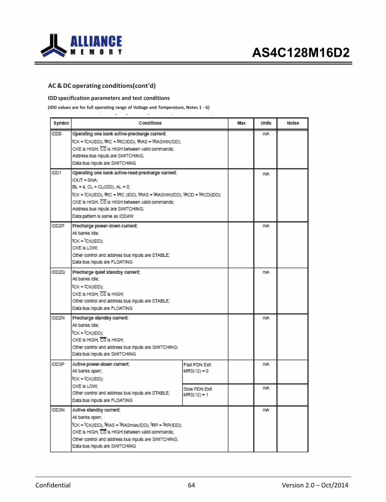
AS4C128M16D2
Confidential 64 Version 2.0 – Oct/2014
AC & DC operating conditions(cont'd)
IDD specification parameters and test conditions
(IDD values are for full operating range of Voltage and Temperature, Notes 1 - 6)
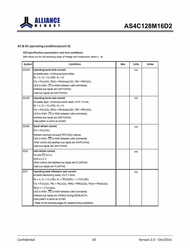
AS4C128M16D2
Confidential 65 Version 2.0 – Oct/2014
AC & DC operating conditions(cont'd)
IDD specification parameters and test conditions
(IDD values are for full operating range of Voltage and Temperature, Notes 1 - 6)
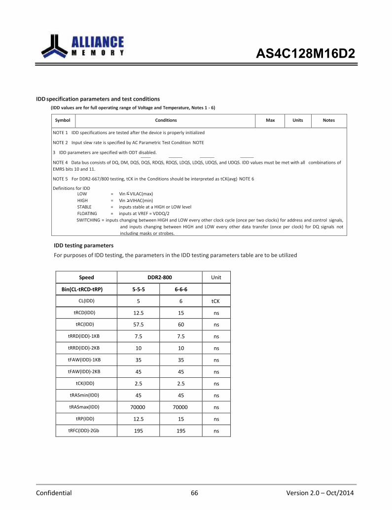
AS4C128M16D2
Confidential 66 Version 2.0 – Oct/2014
IDD specification parameters and test conditions
(IDD values are for full operating range of Voltage and Temperature, Notes 1 - 6)
Symbol Conditions Max Units Notes
NOTE 1 IDD specifications are tested after the device is properly initialized
NOTE 2 Input slew rate is specified by AC Parametric Test Condition NOTE
3 IDD parameters are specified with ODT disabled.
NOTE 4 Data bus consists of DQ, DM, DQS, DQS, RDQS, RDQS, LDQS, LDQS, UDQS, and UDQS. IDD values must be met with all combinations of
EMRS bits 10 and 11.
NOTE 5 For DDR2-667/800 testing, tCK in the Conditions should be interpreted as tCK(avg) NOTE 6
Definitions for IDD LOW = Vin <_ VILAC(max)
HIGH = Vin >_VIHAC(min)
STABLE = inputs stable at a HIGH or LOW level
FLOATING = inputs at VREF = VDDQ/2
SWITCHING = inputs changing between HIGH and LOW every other clock cycle (once per two clocks) for address and control signals,
and inputs changing between HIGH and LOW every other data transfer (once per clock) for DQ signals not
including masks or strobes.
IDD testing parameters
For purposes of IDD testing, the parameters in the IDD testing parameters table are to be utilized
Speed DDR2-800 Unit
Bin(CL-tRCD-tRP) 5-5-5 6-6-6
CL(IDD) 5 6 tCK
tRCD(IDD) 12.5 15 ns
tRC(IDD) 57.5 60 ns
tRRD(IDD)-1KB 7.5 7.5 ns
tRRD(IDD)-2KB 10 10 ns
tFAW(IDD)-1KB 35 35 ns
tFAW(IDD)-2KB 45 45 ns
tCK(IDD) 2.5 2.5 ns
tRASmin(IDD) 45 45 ns
tRASmax(IDD) 70000 70000 ns
tRP(IDD) 12.5 15 ns
tRFC(IDD)-2Gb 195 195 ns
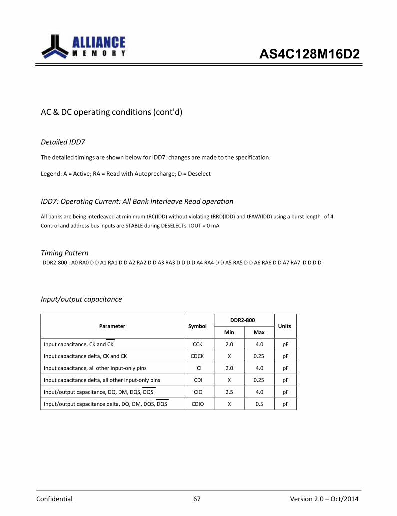
AS4C128M16D2
Confidential 67 Version 2.0 – Oct/2014
AC & DC operating conditions (cont'd)
Detailed IDD7
The detailed timings are shown below for IDD7. changes are made to the specification.
Legend: A = Active; RA = Read with Autoprecharge; D = Deselect
IDD7: Operating Current: All Bank Interleave Read operation
All banks are being interleaved at minimum tRC(IDD) without violating tRRD(IDD) and tFAW(IDD) using a burst length of 4.
Control and address bus inputs are STABLE during DESELECTs. IOUT = 0 mA
Timing Pattern -DDR2-800 : A0 RA0 D D A1 RA1 D D A2 RA2 D D A3 RA3 D D D D A4 RA4 D D A5 RA5 D D A6 RA6 D D A7 RA7 D D D D
Input/output capacitance
Parameter
Symbol
DDR2-800 Units
Min Max
Input capacitance, CK and CK CCK 2.0 4.0 pF
Input capacitance delta, CK and CK CDCK X 0.25 pF
Input capacitance, all other input-only pins CI 2.0 4.0 pF
Input capacitance delta, all other input-only pins CDI X 0.25 pF
Input/output capacitance, DQ, DM, DQS, DQS CIO 2.5 4.0 pF
Input/output capacitance delta, DQ, DM, DQS, DQS CDIO X 0.5 pF
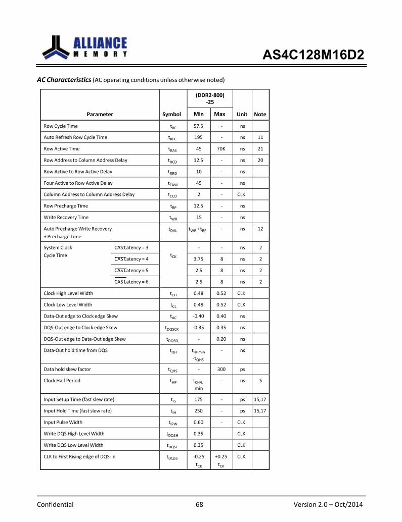
AS4C128M16D2
Confidential 68 Version 2.0 – Oct/2014
AC Characteristics (AC operating conditions unless otherwise noted)
Parameter
Symbol
(DDR2-800) -25
Unit
Note Min Max
Row Cycle Time tRC 57.5 - ns
Auto Refresh Row Cycle Time tRFC 195 - ns 11
Row Active Time tRAS 45 70K ns 21
Row Address to Column Address Delay tRCD 12.5 - ns 20
Row Active to Row Active Delay tRRD 10 - ns
Four Active to Row Active Delay tFAW 45 - ns
Column Address to Column Address Delay tCCD 2 - CLK
Row Precharge Time tRP 12.5 - ns
Write Recovery Time tWR 15 - ns
Auto Precharge Write Recovery
+ Precharge Time
tDAL tWR +tRP - ns 12
System Clock
Cycle Time
CAS Latency = 3
tCK
- - ns 2
CAS Latency = 4 3.75 8 ns 2
CAS Latency = 5 2.5 8 ns 2
CAS Latency = 6 2.5 8 ns 2
Clock High Level Width tCH 0.48 0.52 CLK
Clock Low Level Width tCL 0.48 0.52 CLK
Data-Out edge to Clock edge Skew tAC -0.40 0.40 ns
DQS-Out edge to Clock edge Skew tDQSCK -0.35 0.35 ns
DQS-Out edge to Data-Out edge Skew tDQSQ - 0.20 ns
Data-Out hold time from DQS tQH tHPmin
-tQHS
- ns
Data hold skew factor tQHS - 300 ps
Clock Half Period tHP tCH/L
min
- ns 5
Input Setup Time (fast slew rate) tIS 175 - ps 15,17
Input Hold Time (fast slew rate) tIH 250 - ps 15,17
Input Pulse Width tIPW 0.60 - CLK
Write DQS High Level Width tDQSH 0.35 CLK
Write DQS Low Level Width tDQSL 0.35 CLK
CLK to First Rising edge of DQS-In tDQSS -0.25
tCK
+0.25
tCK
CLK
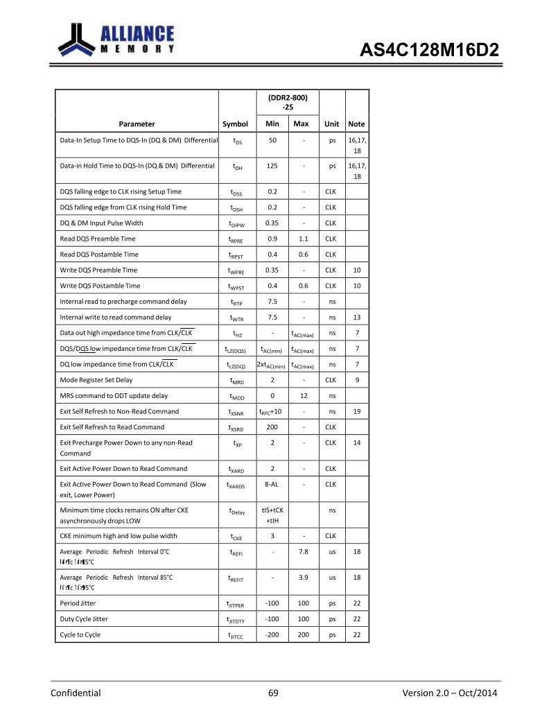
AS4C128M16D2
Confidential 69 Version 2.0 – Oct/2014
Parameter
Symbol
(DDR2-800) -25
Unit
Note Min Max
Data-In Setup Time to DQS-In (DQ & DM) Differential tDS 50 - ps 16,17,
18
Data-in Hold Time to DQS-In (DQ & DM) Differential tDH 125 - ps 16,17,
18
DQS falling edge to CLK rising Setup Time tDSS 0.2 - CLK
DQS falling edge from CLK rising Hold Time tDSH 0.2 - CLK
DQ & DM Input Pulse Width tDIPW 0.35 - CLK
Read DQS Preamble Time tRPRE 0.9 1.1 CLK
Read DQS Postamble Time tRPST 0.4 0.6 CLK
Write DQS Preamble Time tWPRE 0.35 - CLK 10
Write DQS Postamble Time tWPST 0.4 0.6 CLK 10
Internal read to precharge command delay tRTP 7.5 - ns
Internal write to read command delay tWTR 7.5 - ns 13
Data out high impedance time from CLK/CLK tHZ - tAC(max) ns 7
DQS/DQS low impedance time from CLK/CLK tLZ(DQS) tAC(min) tAC(max) ns 7
DQ low impedance time from CLK/CLK tLZ(DQ) 2xtAC(min) tAC(max) ns 7
Mode Register Set Delay tMRD 2 - CLK 9
MRS command to ODT update delay tMOD 0 12 ns
Exit Self Refresh to Non-Read Command tXSNR tRFC+10 - ns 19
Exit Self Refresh to Read Command tXSRD 200 - CLK
Exit Precharge Power Down to any non-Read
Command
tXP 2 - CLK 14
Exit Active Power Down to Read Command tXARD 2 - CLK
Exit Active Power Down to Read Command (Slow
exit, Lower Power)
tXARDS 8-AL - CLK
Minimum time clocks remains ON after CKE
asynchronously drops LOW
tDelay tIS+tCK
+tIH
ns
CKE minimum high and low pulse width tCKE 3 - CLK
Average Periodic Refresh Interval 0°C
Tc 85°C
tREFI - 7.8 us 18
Average Periodic Refresh Interval 85°C
Tc 95°C
tREFIT - 3.9 us 18
Period Jitter tJITPER -100 100 ps 22
Duty Cycle Jitter tJITDTY -100 100 ps 22
Cycle to Cycle tJITCC -200 200 ps 22
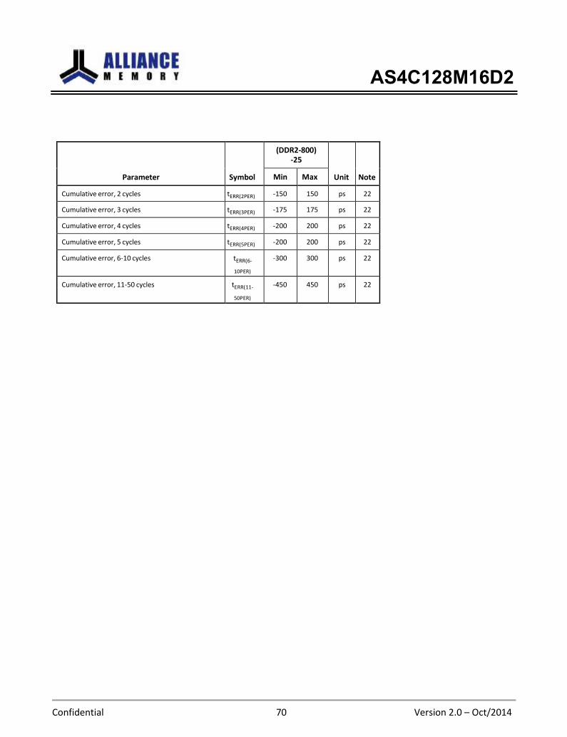
AS4C128M16D2
Confidential 70 Version 2.0 – Oct/2014
Parameter
Symbol
(DDR2-800) -25
Unit
Note Min Max
Cumulative error, 2 cycles tERR(2PER) -150 150 ps 22
Cumulative error, 3 cycles tERR(3PER) -175 175 ps 22
Cumulative error, 4 cycles tERR(4PER) -200 200 ps 22
Cumulative error, 5 cycles tERR(5PER) -200 200 ps 22
Cumulative error, 6-10 cycles tERR(6-
10PER)
-300 300 ps 22
Cumulative error, 11-50 cycles tERR(11-
50PER)
-450 450 ps 22
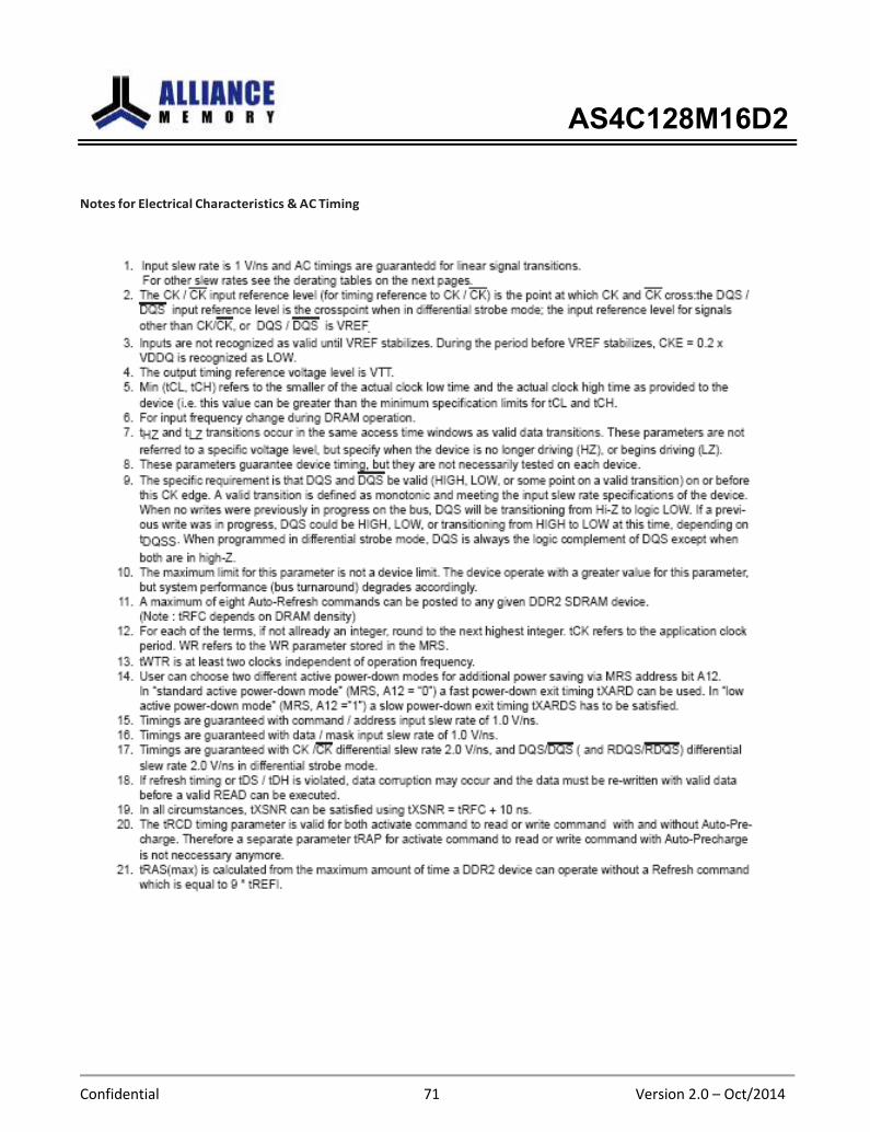
AS4C128M16D2
Confidential 71 Version 2.0 – Oct/2014
Notes for Electrical Characteristics & AC Timing
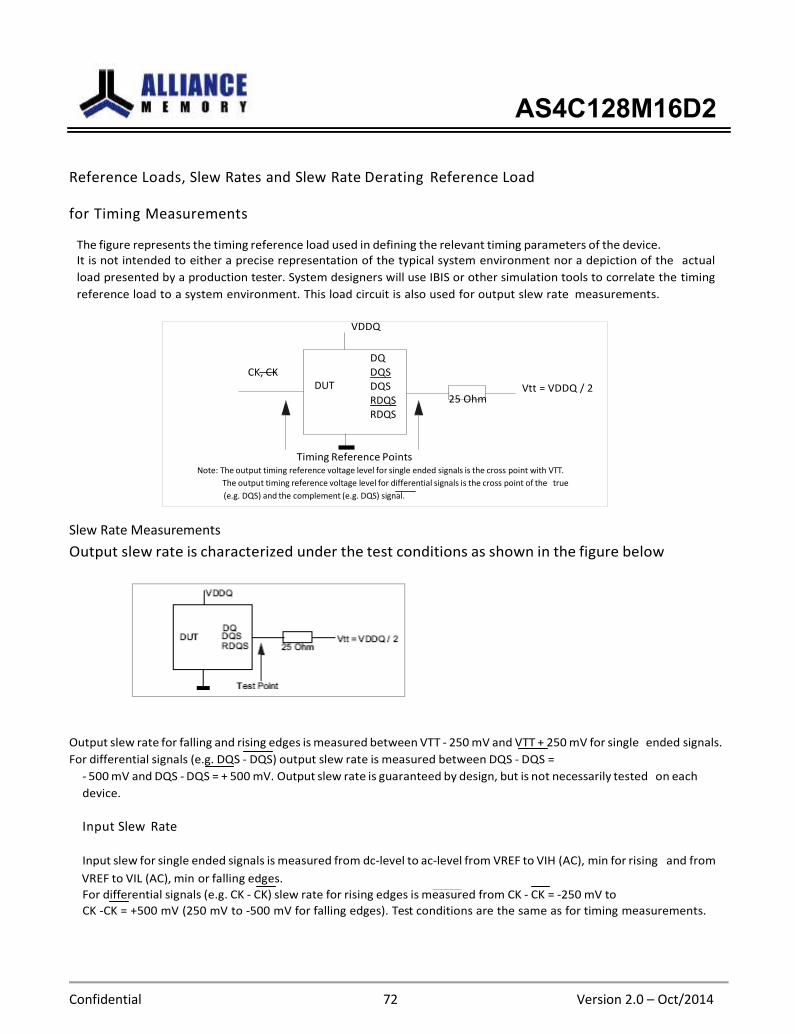
AS4C128M16D2
Confidential 72 Version 2.0 – Oct/2014
Reference Loads, Slew Rates and Slew Rate Derating Reference Load
for Timing Measurements
The figure represents the timing reference load used in defining the relevant timing parameters of the device. It is not intended to either a precise representation of the typical system environment nor a depiction of the actual
load presented by a production tester. System designers will use IBIS or other simulation tools to correlate the timing
reference load to a system environment. This load circuit is also used for output slew rate measurements.
VDDQ
CK, CK
DUT
DQ
DQS DQS RDQS RDQS
25 Ohm
Vtt = VDDQ / 2
Timing Reference Points Note: The output timing reference voltage level for single ended signals is the cross point with VTT.
The output timing reference voltage level for differential signals is the cross point of the true
(e.g. DQS) and the complement (e.g. DQS) signal.
Slew Rate Measurements
Output slew rate is characterized under the test conditions as shown in the figure below
Output slew rate for falling and rising edges is measured between VTT - 250 mV and VTT + 250 mV for single ended signals.
For differential signals (e.g. DQS - DQS) output slew rate is measured between DQS - DQS =
- 500 mV and DQS - DQS = + 500 mV. Output slew rate is guaranteed by design, but is not necessarily tested on each
device.
Input Slew Rate
Input slew for single ended signals is measured from dc-level to ac-level from VREF to VIH (AC), min for rising and from
VREF to VIL (AC), min or falling edges.
For differential signals (e.g. CK - CK) slew rate for rising edges is measured from CK - CK = -250 mV to
CK -CK = +500 mV (250 mV to -500 mV for falling edges). Test conditions are the same as for timing measurements.
AS4C128M16D2
Confidential 73 Version 2.0 – Oct/2014
Package Diagram (x16) 84-Ball Fine Pitch Ball Grid Array Outline
AS4C128M16D2
Confidential 74 Version 2.0 – Oct/2014
Alliance Memory Inc. reserves the rights to change the specifications and products without notice.
Alliance Memory, Inc., 551 Taylor Way, Suite #1, San Carlos, CA 94070, USA Tel: +1 650 610 6800 Fax: +1 650 620 9211