Embed Size (px)
Citation preview
16-Bit LED Driver CS8816
1 Rev. 1.5
Chiplus reserves the right to change product or specification without notice.
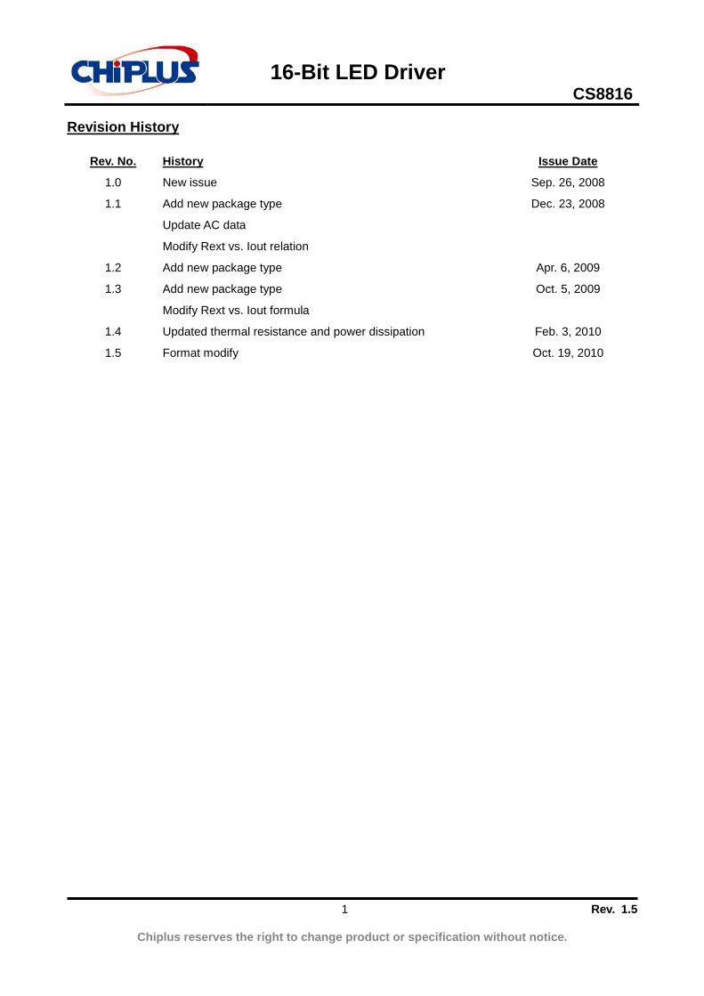
Revision History
Rev. No. History Issue Date
1.0 New issue Sep. 26, 2008
1.1 Add new package type
Update AC data
Modify Rext vs. Iout relation
Dec. 23, 2008
1.2 Add new package type Apr. 6, 2009
1.3 Add new package type
Modify Rext vs. Iout formula
Oct. 5, 2009
1.4 Updated thermal resistance and power dissipation Feb. 3, 2010
1.5 Format modify Oct. 19, 2010

16-Bit LED Driver CS8816
2 Rev. 1.5
Chiplus reserves the right to change product or specification without notice.
CS8816(AF/AN/CP/AM/AN-1) 16-Bit Constant Current LED Driver with 3.0V to 5.5V Supply Voltage
� Description
The CS8816 is a 16-Bit constant current LED driver IC which is designed for LED displays. The output
current can be adjusted by using an external resistor. All outputs will have the same current drive level which
is crucial in LED display application. This driver has built-in 16-bit constant current outputs, a 16-bit shift
register, and a 16-bit latch circuit. These drivers have been designed by using CMOS process.
� Feature � Output current capability: 70mA each output
� Constant current range: 5mA to 70mA
� For common anode LED application
� Power supply voltage range VDD=3.0V to 5.5V
� Maximum output drain voltage 7.0V
� Serial data transfer rate: 25MHz(Cascade Connection)
� Operating temperature range: -40 to 85 degree C
� Output current accuracy:
Between Bits : < +-1.5 %
Between ICs: < +-4 %
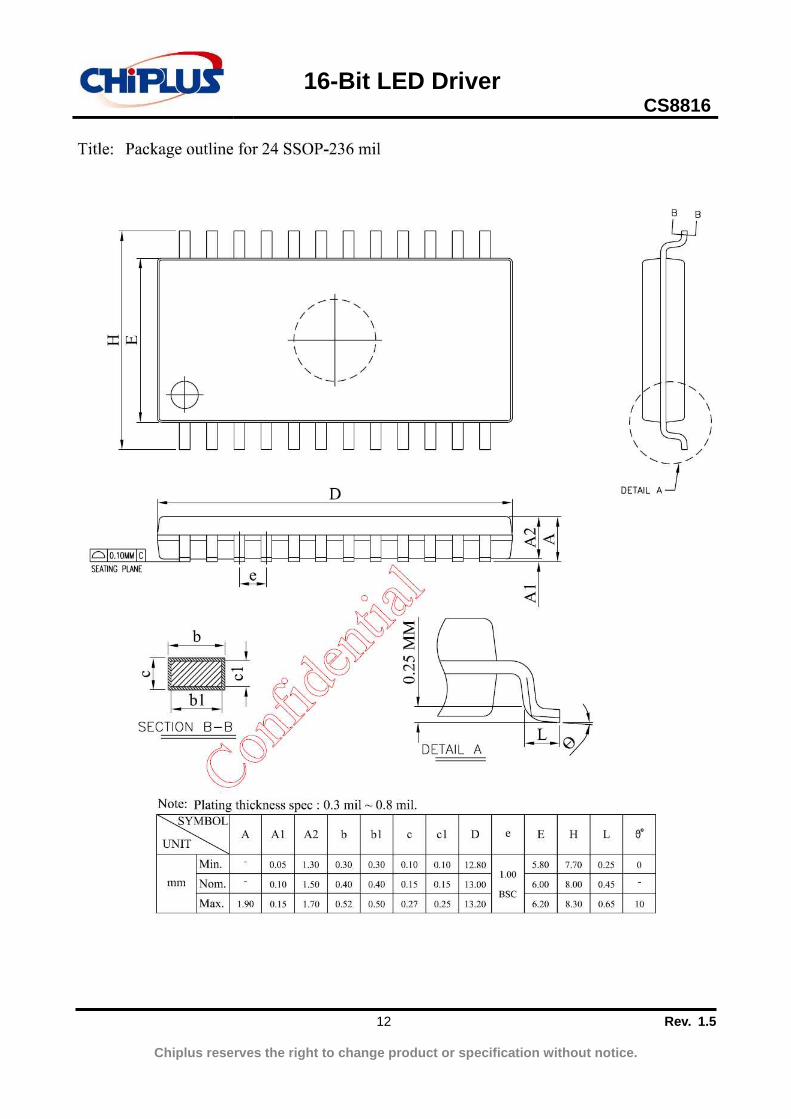
� Product Family CS8816AF ------- 24SSOP(236mil, 1.0mm lead-pitch)
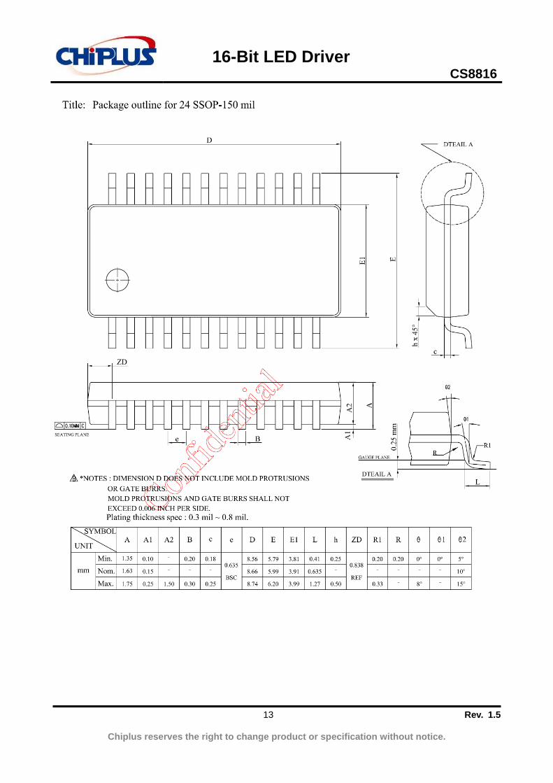
CS8816AN ------- 24SSOP(150mil, 0.64mm lead-pitch)
CS8816CP ------- 24Shrink PDIP(300mil, 1.78mm lead-pitch)
CS8816AM ------- 24SOP(300mil, 1.27mm lead-pitch)
CS8816AN-1 ------- 24SSOP(150mil, 0.64mm lead-pitch)

16-Bit LED Driver CS8816
3 Rev. 1.5
Chiplus reserves the right to change product or specification without notice.
� Pin Assignment
AF/AN/CP/AM AN-1
� Block Diagram
� Truth Table CLOCK LATCH ENABLE SERIAL-IN OUT0---OUT7---OUT15 SERIAL-OUT
Positive edge H L Dn /Dn---/Dn-7---/Dn-15 Dn-15
Positive edge L L Dn+1 No Change Dn-14
Positive edge H L Dn+2 /Dn+2---/Dn-5---/Dn-13 Dn-13
Negative edge X L Dn+3 /Dn+2---/Dn-5---/Dn-13 Dn-13
Negative edge X H Dn+3 Off Dn-13
16-Bit LED Driver CS8816
4 Rev. 1.5
Chiplus reserves the right to change product or specification without notice.
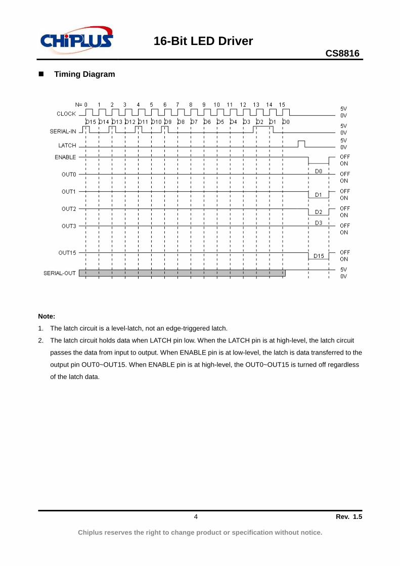
� Timing Diagram
Note:
1. The latch circuit is a level-latch, not an edge-triggered latch.
2. The latch circuit holds data when LATCH pin low. When the LATCH pin is at high-level, the latch circuit
passes the data from input to output. When ENABLE pin is at low-level, the latch is data transferred to the
output pin OUT0~OUT15. When ENABLE pin is at high-level, the OUT0~OUT15 is turned off regardless
of the latch data.

16-Bit LED Driver CS8816
5 Rev. 1.5
Chiplus reserves the right to change product or specification without notice.
� Pin Description Pin No. Pin Name Function
1 GND GND Pin.
2 SERIAL-IN Serial input data pin.
3 CLOCK Clock input terminal for shift register, rising edge trigger.
4 LATCH Data latch input pin. When LATCH=High-level, data is passed to
OUT0~OUT15, when LATCH=Low-level, data is latched.
5~20 OUT0~OUT15 16 constant current output pin to drive common anode LEDs.
21 ENABLE Data output enable pin, when ENABLE=High-level, all OUT0~OUT15 are
turned off, and when ENABLE=Low-level, all OUT0~OUT15 are enabled.
22 SERIAL-OUT Serial data output pin for cascade operation.
23 R-EXT The external resistor connection pin to adjust the output current.
24 VDD 3.0V~5.5V supply voltage pin.
� Equivalent Circuits of I/O Pins

16-Bit LED Driver CS8816
6 Rev. 1.5
Chiplus reserves the right to change product or specification without notice.
� Absolute Maximum Ratings Characteristics Symbol Rating Unit
Supply Voltage VDD +7.0 V
Input Voltage Vin -0.4 to VDD+0.4 V
Output Current Iout +70 mA
Output Voltage Vout -0.5 to 7.0 V
GND Pin Current IGND 1120 mA
Clock Frequency fCLK 25 MHz
Power Dissipation (On PCB, Ta=45C)
Pd AF: 2.36 AN: 1.94 CP: 1.91 AM: 1.76
W
Thermal Resistance (On PCB, Ta=45C)
Rth(j-a) AF: 44.4 AN: 54.25 CP: 55.07 AM: 59.6
/W℃
Operating Temperature Top -40 to 85 ℃
Storage Temperature Tstg -55 to 150 ℃
� Recommended Operating Condition Characteristics Symbol Condition Min Typ Max Unit
Supply Voltage VDD 3.0 5.0 5.5 V
Output Voltage VOUT 7.0 V
Output Current IOUT
IOL
IOH
OUTn
SERIAL-OUT Vol=0.5V
SERIAL-OUT Voh=4.3V
70
2.5
-2.0
mA
Input Voltage VIH
VIL
0.7VDD
-0.3
VDD+0.3
0.3VDD
V
Clock Frequency fCLK VDD=5.0V, Cascade connection
VDD=3.0V, Cascade connection
25
20
MHz
Latch Pulse Width twLatch VDD=4.5V ~ 5.5V 15 ns
Clock Pulse Width twCLOCK VDD=4.5V ~ 5.5V 15 ns
Set-Up Time for Data tSETUP3 VDD=4.5V ~ 5.5V 20 ns
Set-Up Time for Latch tSETUP2 VDD=4.5V ~ 5.5V 15 ns
Set-Up Time for Clock tSETUP1 VDD=4.5V ~ 5.5V 20 ns
Hold Time for Data tHOLD VDD=4.5V ~ 5.5V 20 ns
16-Bit LED Driver CS8816
7 Rev. 1.5
Chiplus reserves the right to change product or specification without notice.
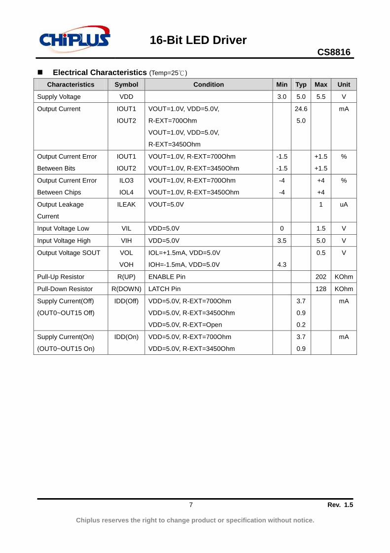
� Electrical Characteristics (Temp=25 )℃ Characteristics Symbol Condition Min Typ Max Unit
Supply Voltage VDD 3.0 5.0 5.5 V
Output Current IOUT1
IOUT2
VOUT=1.0V, VDD=5.0V,
R-EXT=700Ohm
VOUT=1.0V, VDD=5.0V,
R-EXT=3450Ohm
24.6
5.0
mA
Output Current Error
Between Bits
IOUT1
IOUT2
VOUT=1.0V, R-EXT=700Ohm
VOUT=1.0V, R-EXT=3450Ohm
-1.5
-1.5
+1.5
+1.5
%
Output Current Error
Between Chips
ILO3
IOL4
VOUT=1.0V, R-EXT=700Ohm
VOUT=1.0V, R-EXT=3450Ohm
-4
-4
+4
+4
%
Output Leakage
Current
ILEAK VOUT=5.0V 1 uA
Input Voltage Low VIL VDD=5.0V 0 1.5 V
Input Voltage High VIH VDD=5.0V 3.5 5.0 V
Output Voltage SOUT VOL
VOH
IOL=+1.5mA, VDD=5.0V
IOH=-1.5mA, VDD=5.0V
4.3
0.5 V
Pull-Up Resistor R(UP) ENABLE Pin 202 KOhm
Pull-Down Resistor R(DOWN) LATCH Pin 128 KOhm
Supply Current(Off)
(OUT0~OUT15 Off)
IDD(Off) VDD=5.0V, R-EXT=700Ohm
VDD=5.0V, R-EXT=3450Ohm
VDD=5.0V, R-EXT=Open
3.7
0.9
0.2
mA
Supply Current(On)
(OUT0~OUT15 On)
IDD(On) VDD=5.0V, R-EXT=700Ohm
VDD=5.0V, R-EXT=3450Ohm
3.7
0.9
mA

16-Bit LED Driver CS8816
8 Rev. 1.5
Chiplus reserves the right to change product or specification without notice.
� Switching Characteristics (Temp=25 ,℃ VDD=5V, VIH=3.5V, VIL=0V, R-EXT=860Ohm)
Characteristics Symbol Condition Min Typ Max Unit
tpLH1 CLK-OUTn, LATCH=“H”, ENABLE=“L” 40 60 ns
tpLH2 LATCH-OUTn, ENABLE=“L” 35 50 ns
tpLH3 ENABLE-OUTn, LATCH=“H” 20 30 ns
tpLH CLK-SERIAL OUT 30 40 ns
tpHL1 CLK-OUTn, LATCH=“H”, ENABLE=“L” 80 125 ns
tpHL2 LATCH-OUTn, ENABLE=“L” 75 120 ns
tpHL3 ENABLE-OUTn, LATCH=“H” 130 180 ns
Propagation Delay
tpHL CLK-SERIAL OUT 30 40 ns
tW(CLOCK) CLOCK 15 ns
tW(LATCH) LATCH 10 ns Pulse Width
tW(ENABLE) ENABLE 180 ns
Output Rise Time tor Voltage waveform 10%~90% 30 75 150 ns
Output Fall Time tof Voltage waveform 90%~10% 10 20 40 ns
Max CLK Rise Time tr 480 ns
Max CLK Fall Time tf 480 ns
� Test Circuit (RL=162Ohm, CL=10pf, VL=5.0V)

16-Bit LED Driver CS8816
9 Rev. 1.5
Chiplus reserves the right to change product or specification without notice.
� Timing Waveform
16-Bit LED Driver CS8816
10 Rev. 1.5
Chiplus reserves the right to change product or specification without notice.
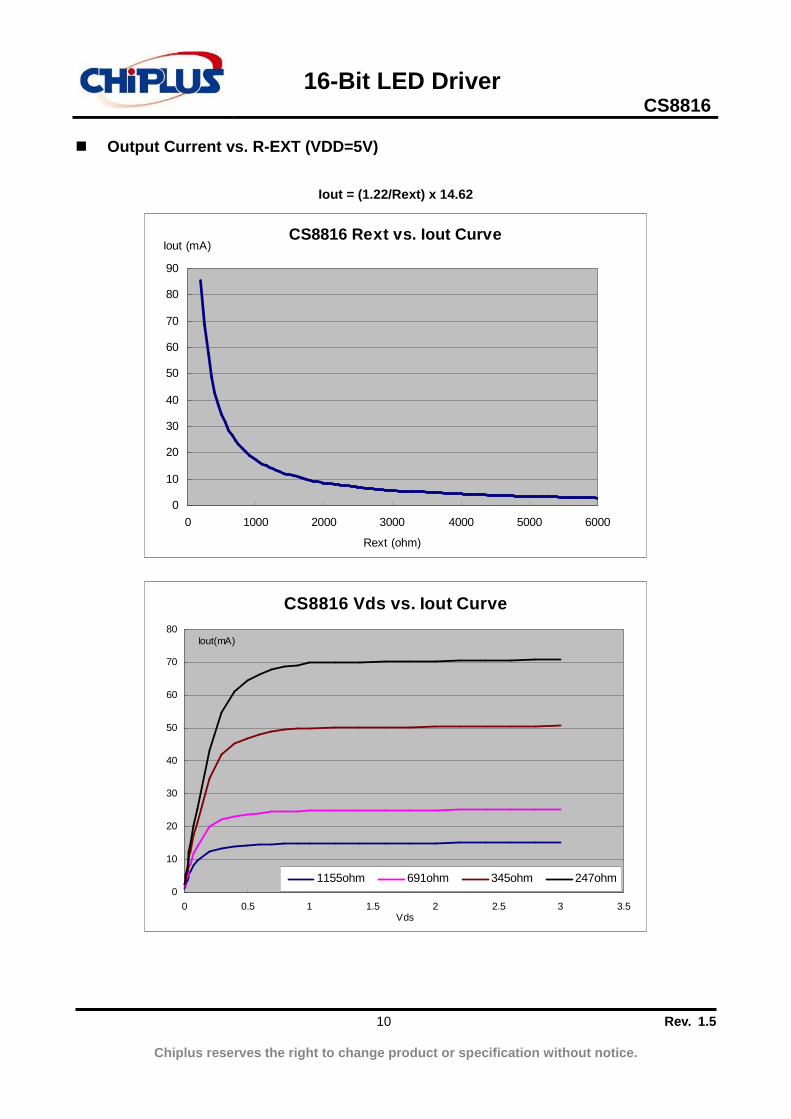
� Output Current vs. R-EXT (VDD=5V)
Iout = (1.22/Rext) x 14.62
CS8816 Rext vs. Iout Curve
0
10
20
30
40
50
60
70
80
90
0 1000 2000 3000 4000 5000 6000
Rext (ohm)
Iout (mA)
CS8816 Vds vs. Iout Curve
0
10
20
30
40
50
60
70
80
0 0.5 1 1.5 2 2.5 3 3.5Vds
Iout(mA)
1155ohm 691ohm 345ohm 247ohm
16-Bit LED Driver CS8816
11 Rev. 1.5
Chiplus reserves the right to change product or specification without notice.
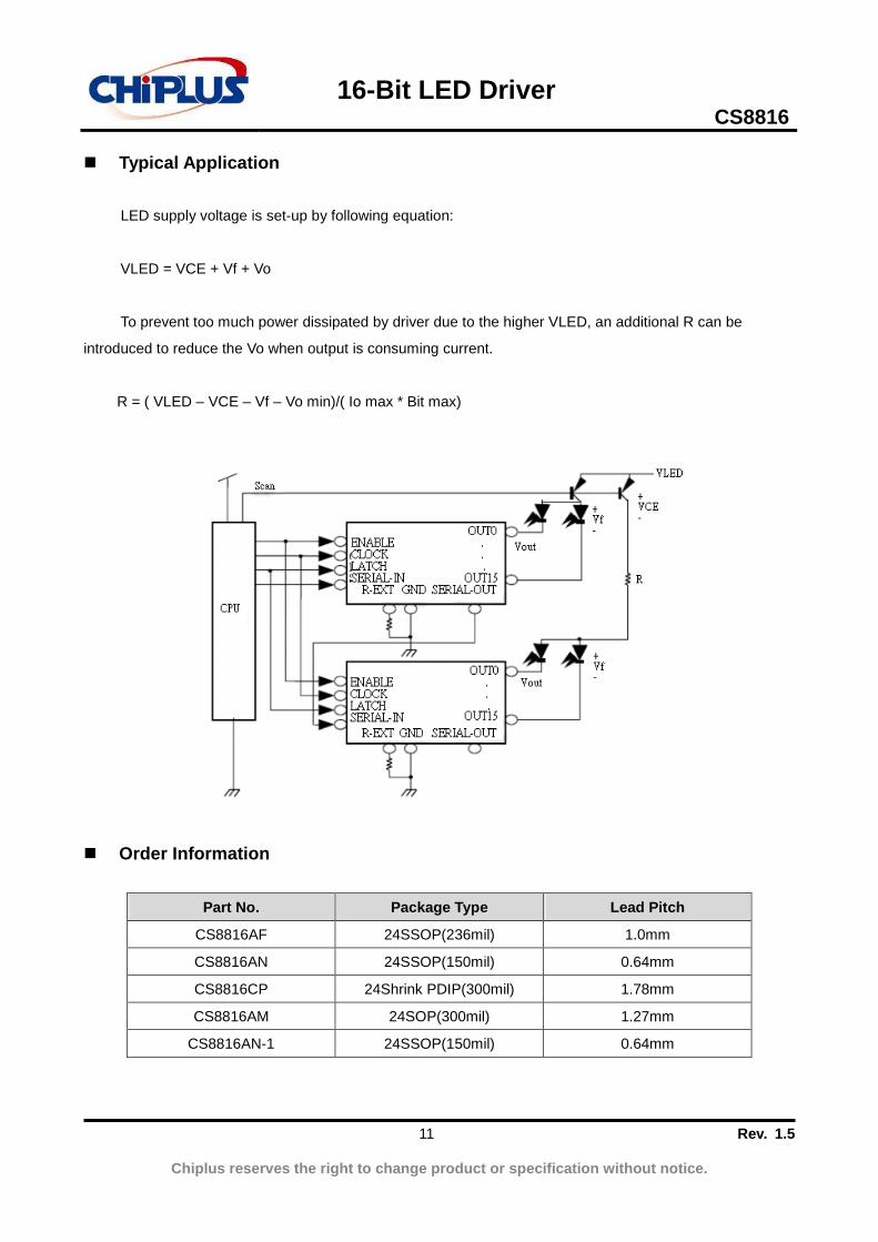
� Typical Application
LED supply voltage is set-up by following equation:
VLED = VCE + Vf + Vo
To prevent too much power dissipated by driver due to the higher VLED, an additional R can be
introduced to reduce the Vo when output is consuming current.
R = ( VLED – VCE – Vf – Vo min)/( Io max * Bit max)
� Order Information
Part No. Package Type Lead Pitch
CS8816AF 24SSOP(236mil) 1.0mm
CS8816AN 24SSOP(150mil) 0.64mm
CS8816CP 24Shrink PDIP(300mil) 1.78mm
CS8816AM 24SOP(300mil) 1.27mm
CS8816AN-1 24SSOP(150mil) 0.64mm
16-Bit LED Driver CS8816
12 Rev. 1.5
Chiplus reserves the right to change product or specification without notice.
16-Bit LED Driver CS8816
13 Rev. 1.5
Chiplus reserves the right to change product or specification without notice.

16-Bit LED Driver CS8816
14 Rev. 1.5
Chiplus reserves the right to change product or specification without notice.

16-Bit LED Driver CS8816
15 Rev. 1.5
Chiplus reserves the right to change product or specification without notice.