Embed Size (px)
DESCRIPTION
Rf Ampl Design
Citation preview

HIGH EFFICIENCY RF AMPLIFIER DESIGN WITH HARMONIC TUNED TECHNIQUE
Supervisor: Professor K.K. ChengAssociate Examiner: Professor H.K. TsangStudent: Ko Lai Kin, KenSID: 06504164
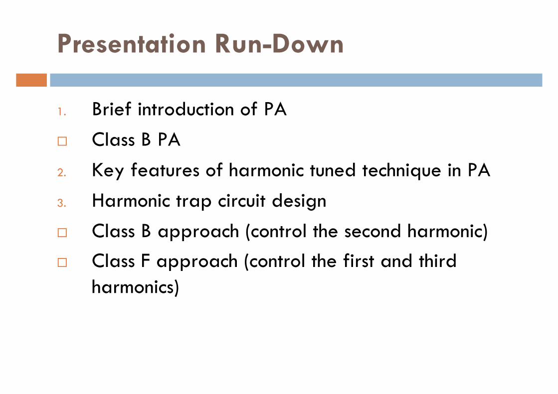
Presentation Run-Down
1. Brief introduction of PAClass B PA
2. Key features of harmonic tuned technique in PA3. Harmonic trap circuit design
Class B approach (control the second harmonic)Class F approach (control the first and third harmonics)
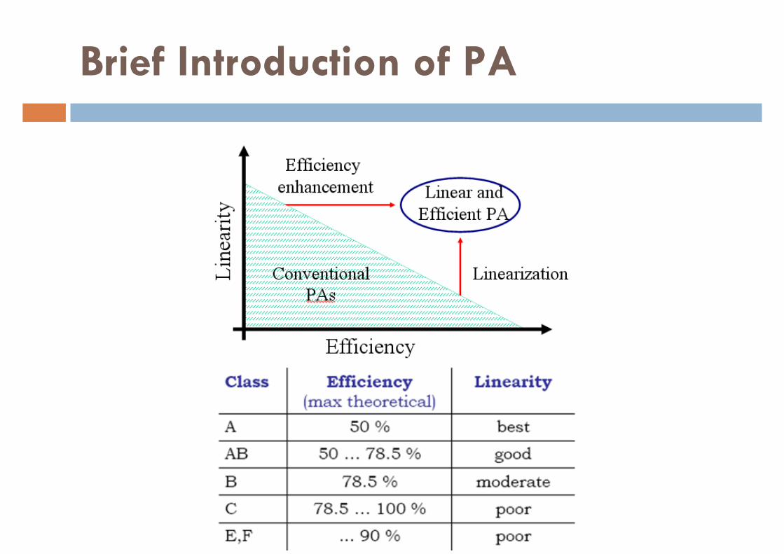
Brief Introduction of PA
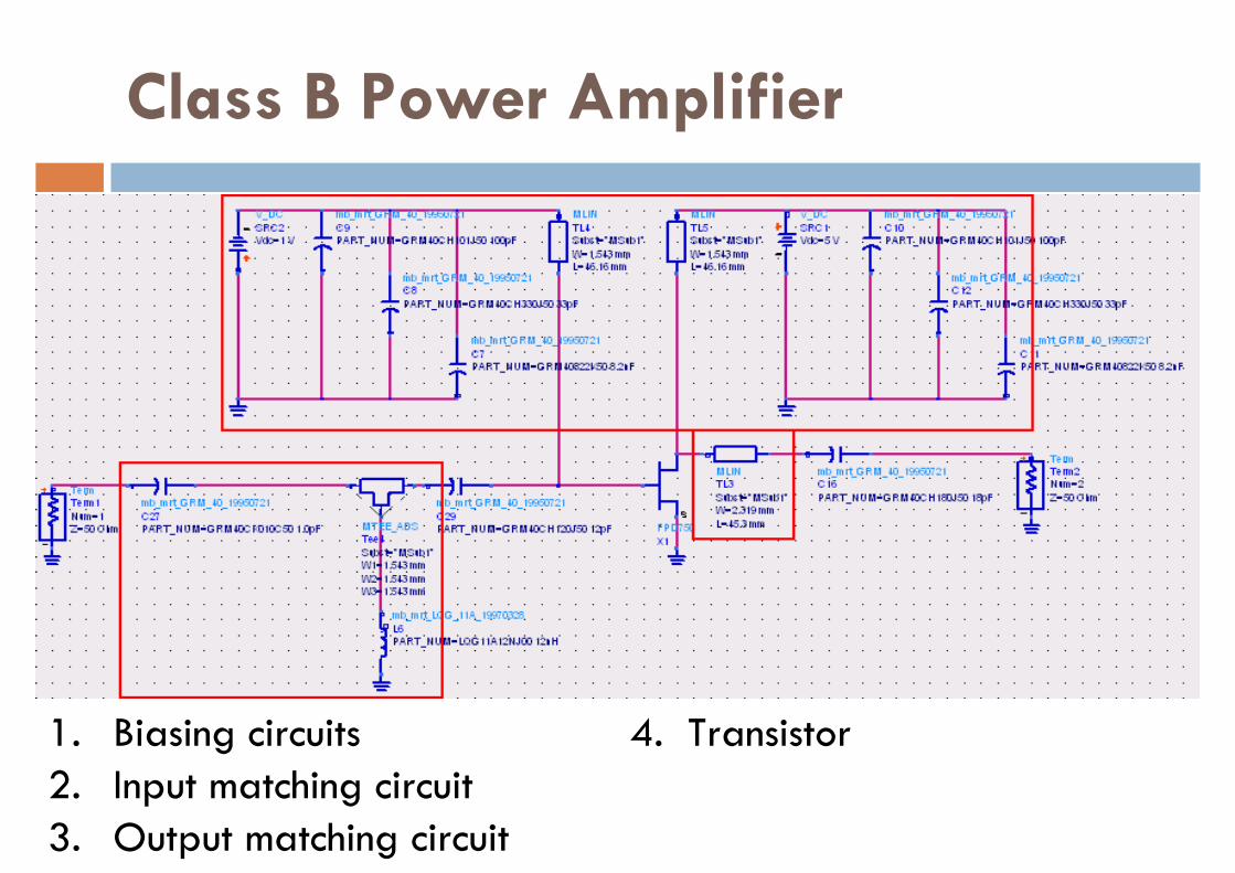
Class B Power Amplifier
1. Biasing circuits 4. Transistor2. Input matching circuit3. Output matching circuit
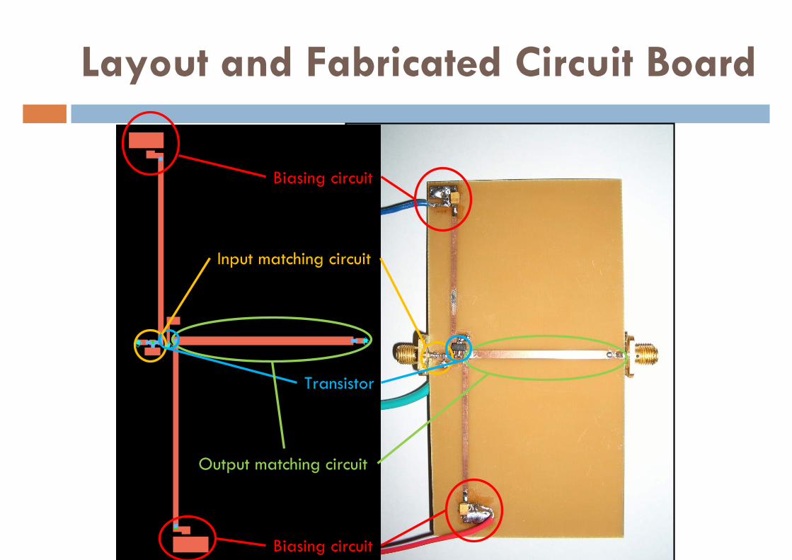
Layout and Fabricated Circuit Board
Biasing circuit
Biasing circuit
Output matching circuit
Input matching circuit
Transistor
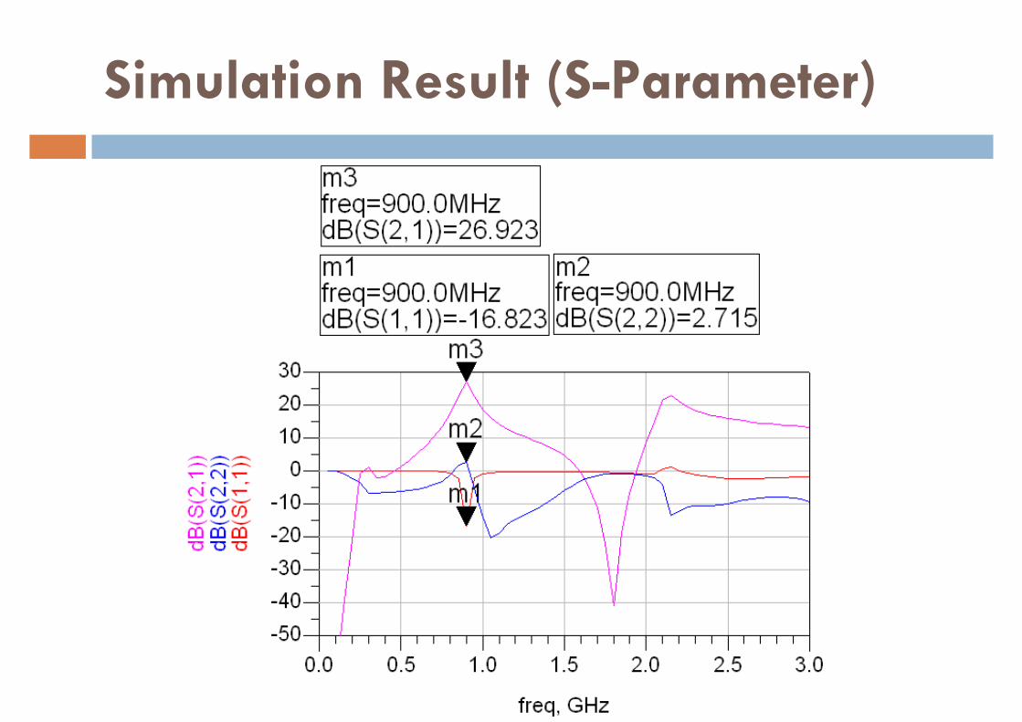
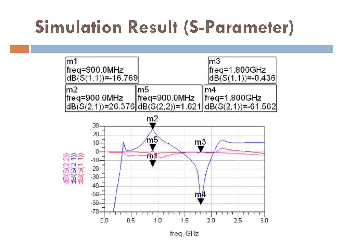
Simulation Result (S-Parameter)
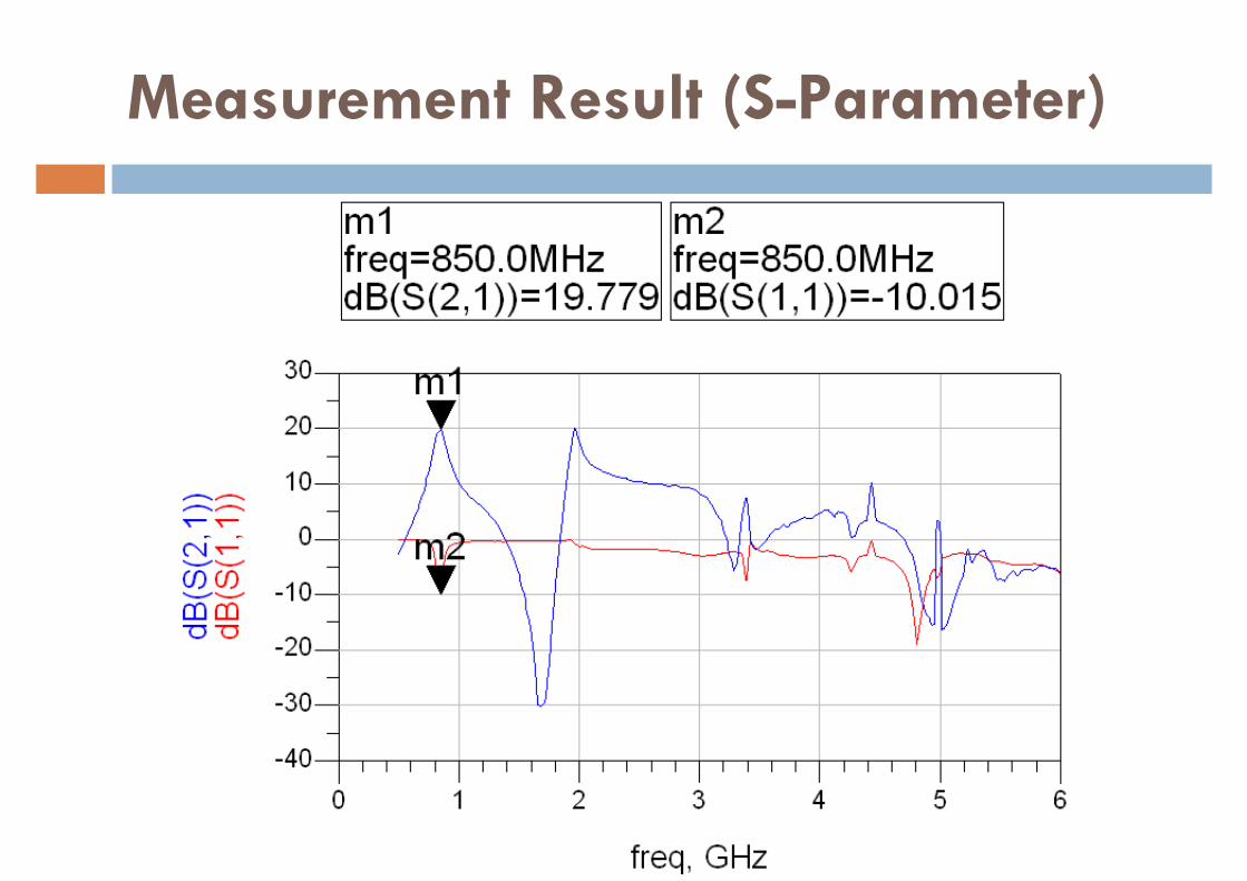
Measurement Result (S-Parameter)
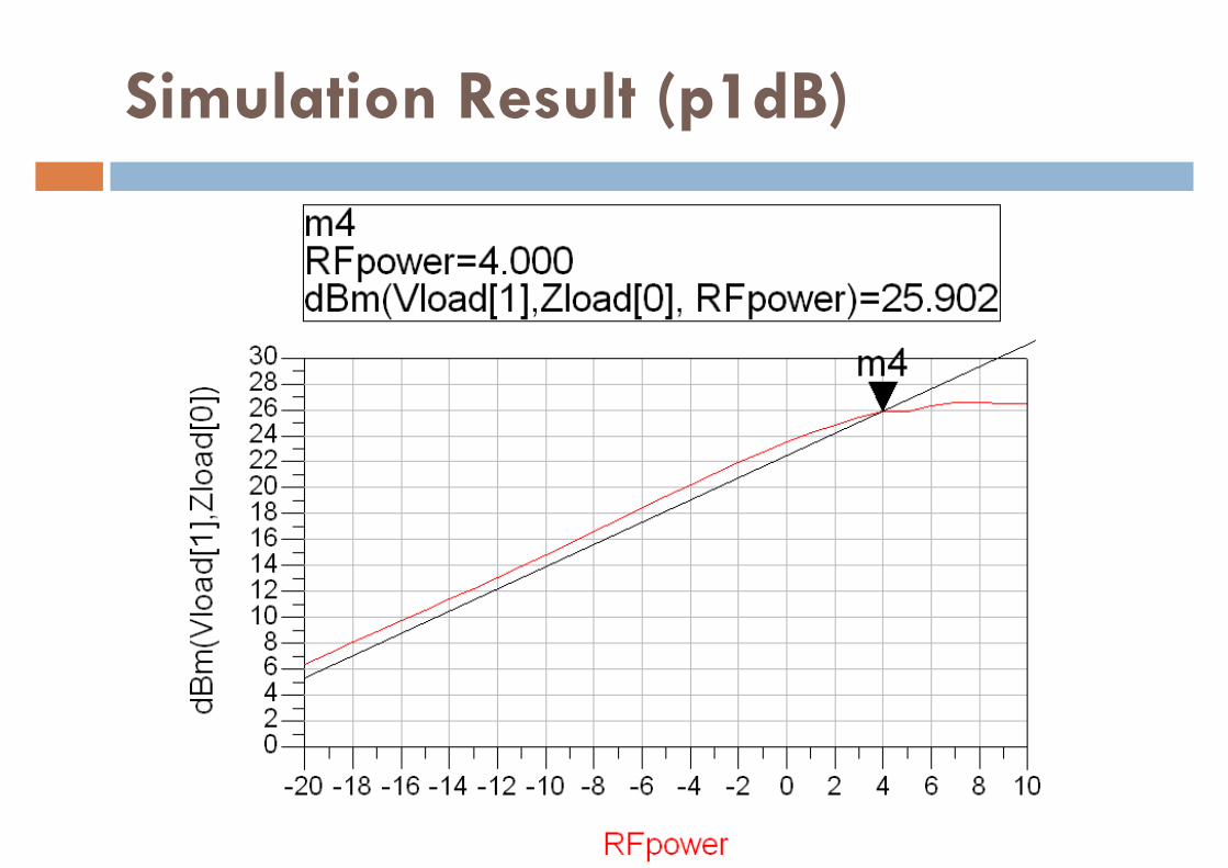
Simulation Result (p1dB)
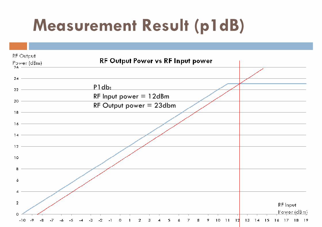
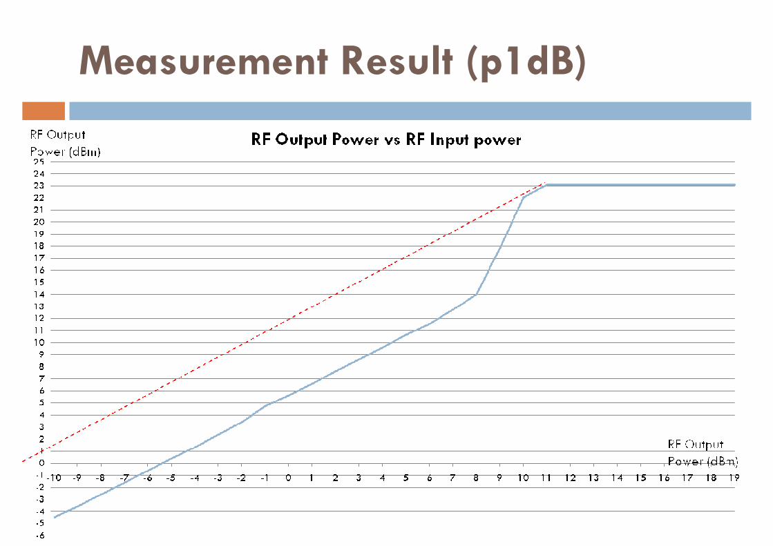
Measurement Result (p1dB)
P1db:RF Input power = 12dBmRF Output power = 23dbm
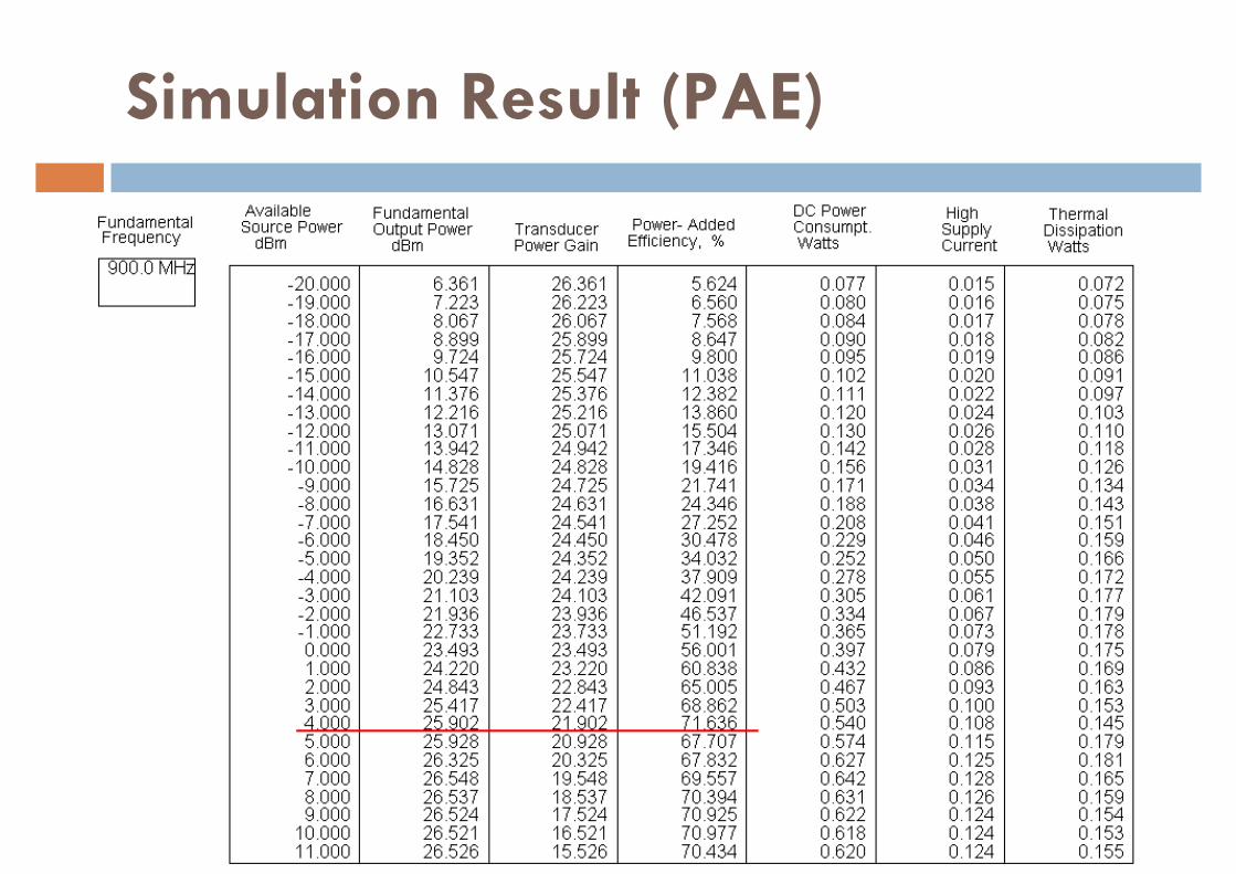
Simulation Result (PAE)
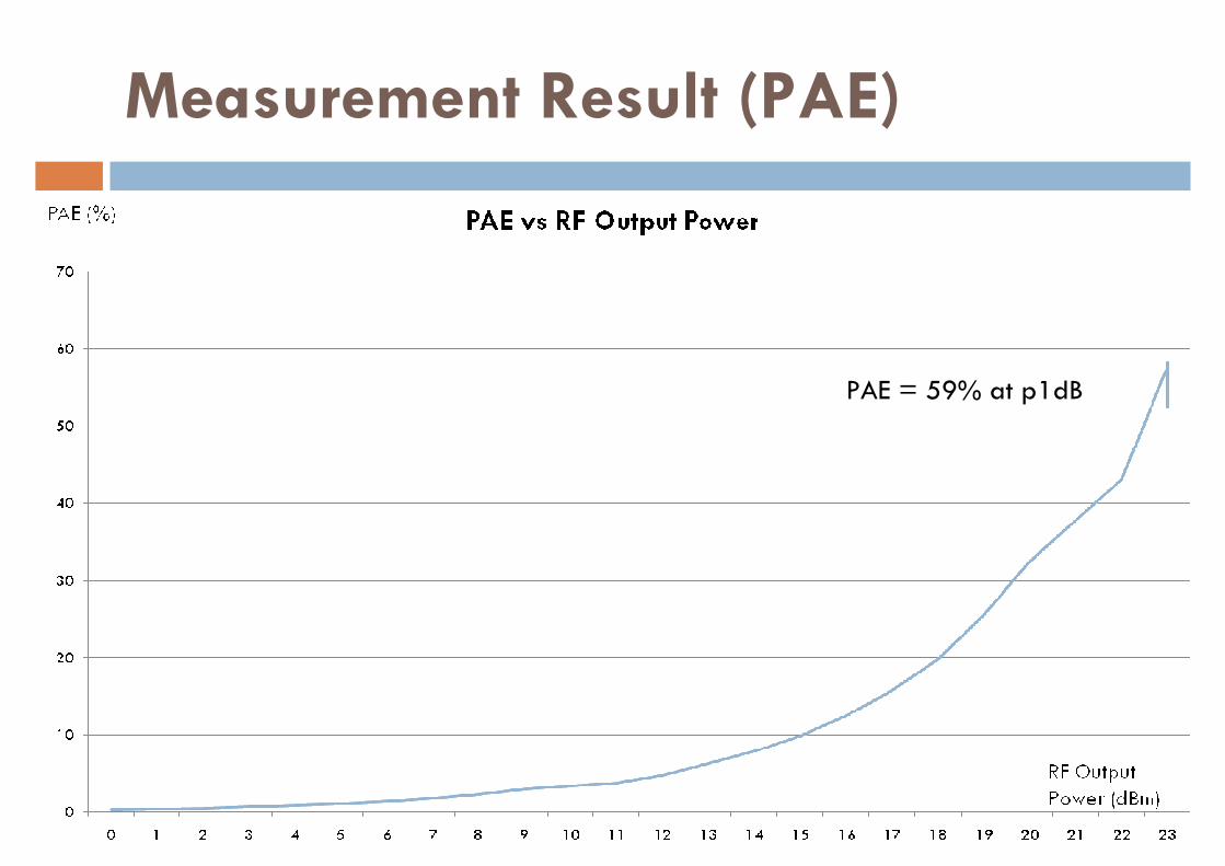
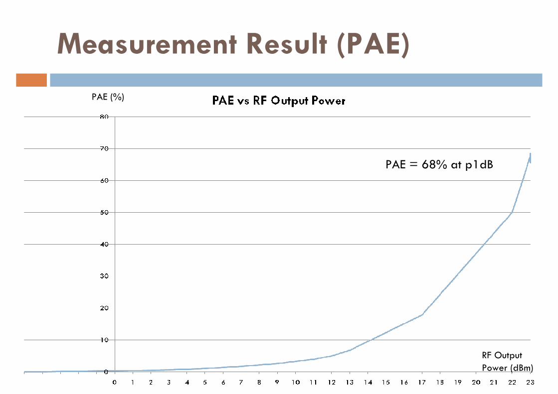
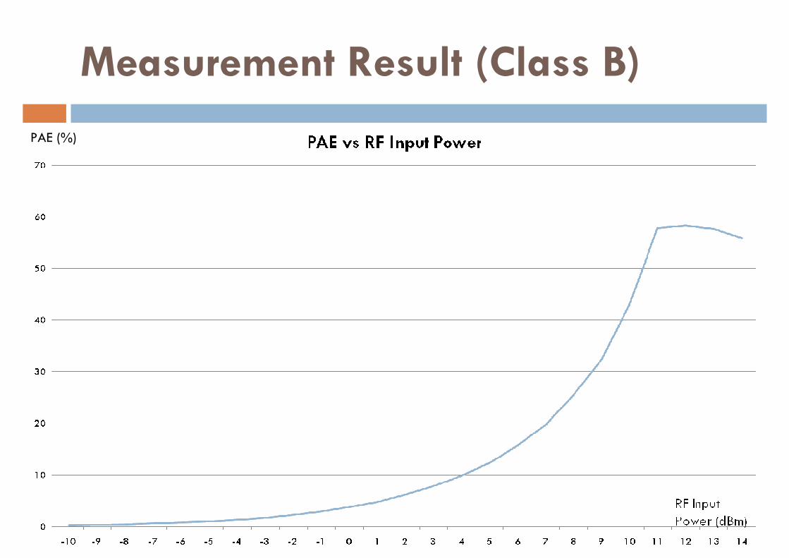
Measurement Result (PAE)
PAE = 59% at p1dB
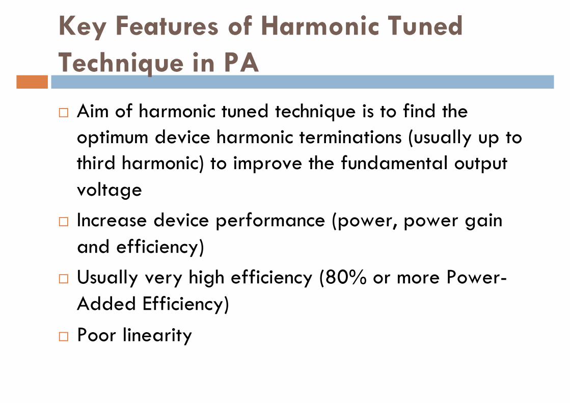
Key Features of Harmonic Tuned Technique in PA
Aim of harmonic tuned technique is to find the optimum device harmonic terminations (usually up to third harmonic) to improve the fundamental output voltageIncrease device performance (power, power gain and efficiency)Usually very high efficiency (80% or more Power-Added Efficiency)Poor linearity
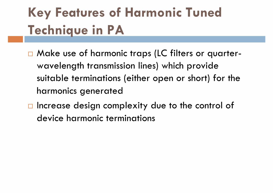
Key Features of Harmonic Tuned Technique in PA
Make use of harmonic traps (LC filters or quarter-wavelength transmission lines) which provide suitable terminations (either open or short) for the harmonics generatedIncrease design complexity due to the control of device harmonic terminations
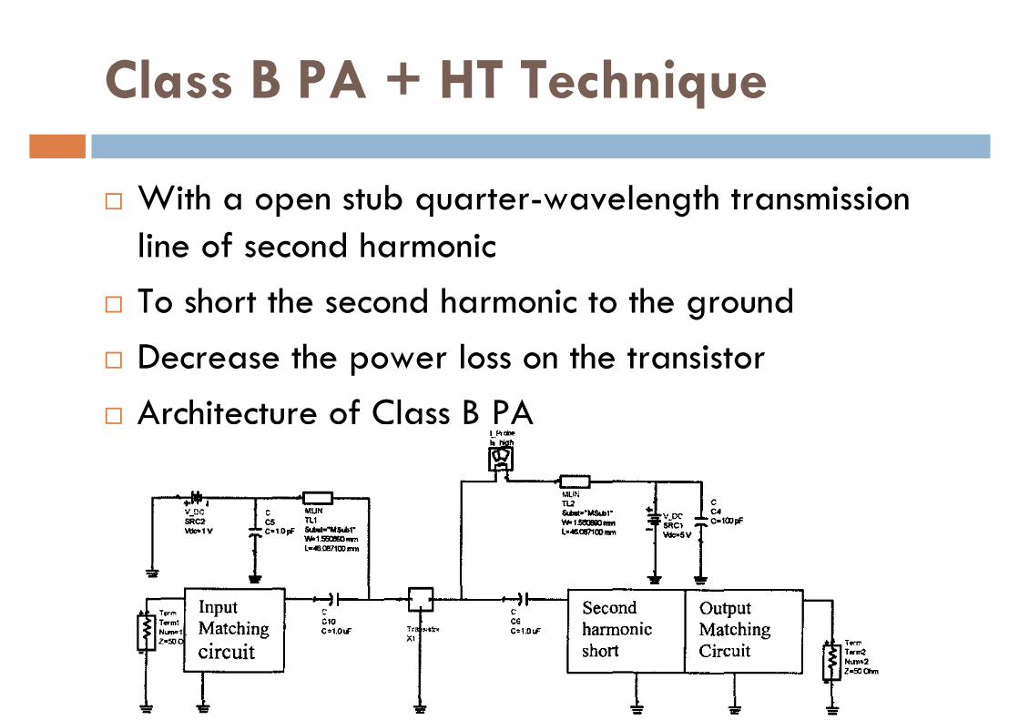
Class B PA + HT Technique
With a open stub quarter-wavelength transmission line of second harmonicTo short the second harmonic to the groundDecrease the power loss on the transistorArchitecture of Class B PA
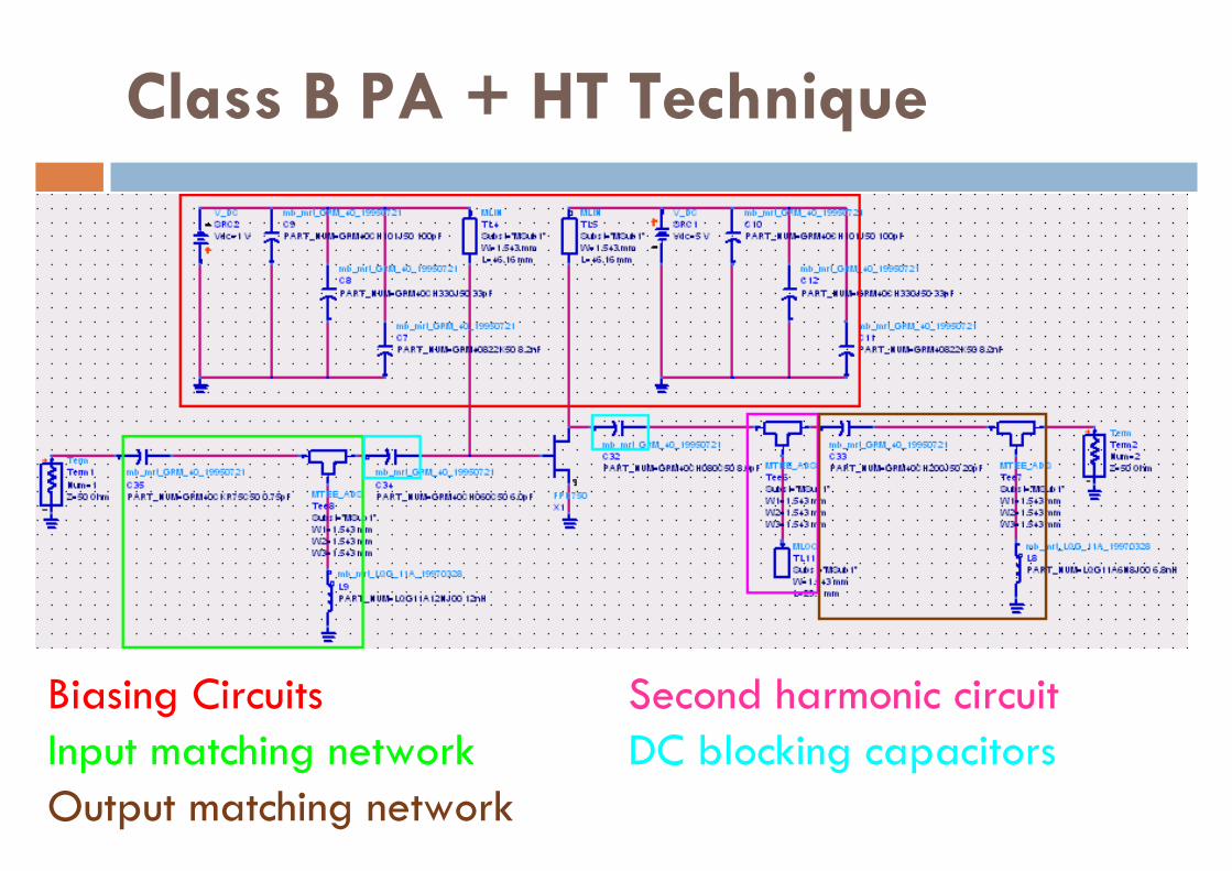
Class B PA + HT Technique
Biasing Circuits Second harmonic circuitInput matching network DC blocking capacitorsOutput matching network
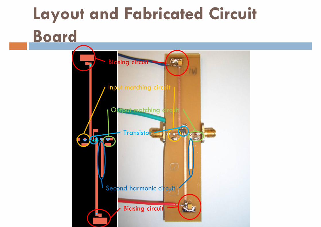
Layout and Fabricated Circuit Board
Biasing circuit
Biasing circuit
Output matching circuit
Input matching circuit
Transistor
Second harmonic circuit
Simulation Result (S-Parameter)
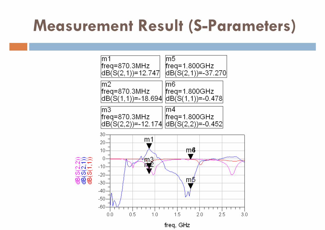
Measurement Result (S-Parameters)
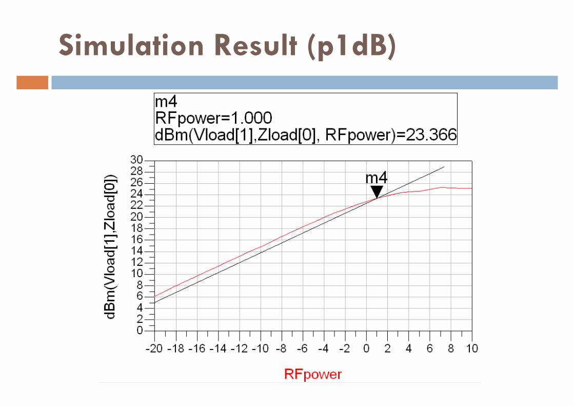
Simulation Result (p1dB)
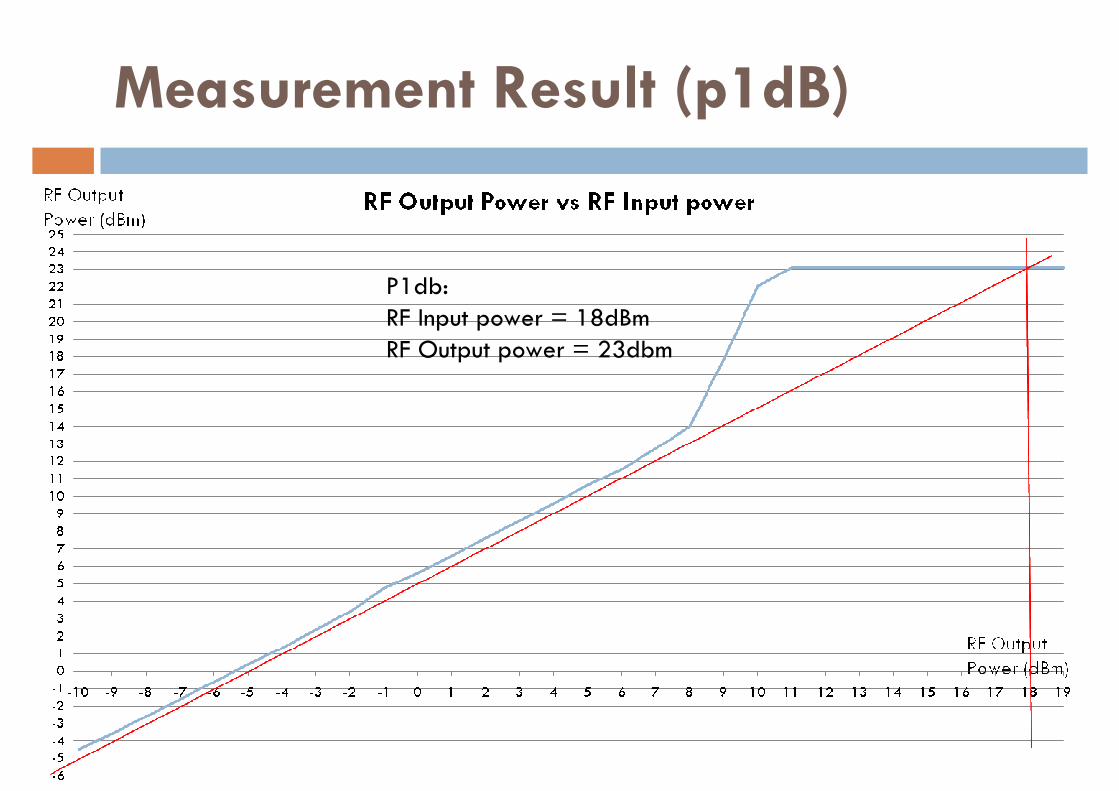
Measurement Result (p1dB)
P1db:RF Input power = 18dBmRF Output power = 23dbm
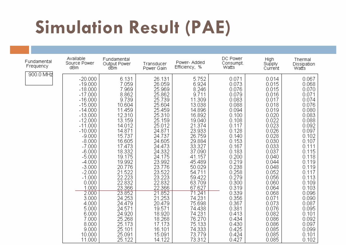
Simulation Result (PAE)
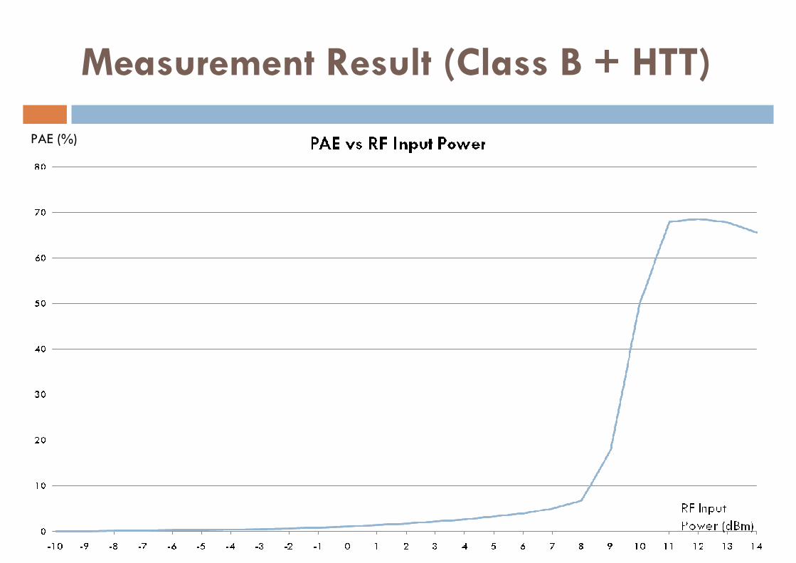
Measurement Result (PAE)
PAE (%)
RF Output Power (dBm)
PAE = 68% at p1dB
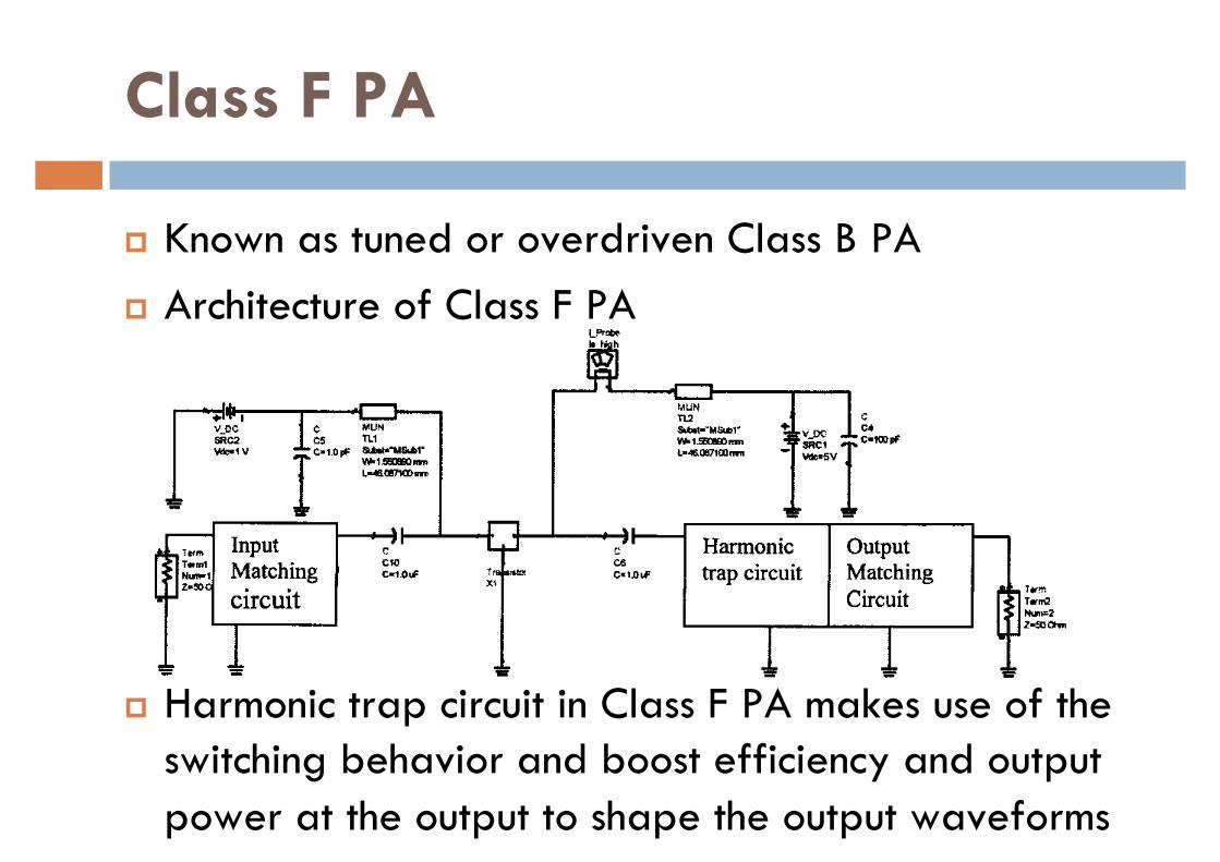
Class F PA
Known as tuned or overdriven Class B PAArchitecture of Class F PA
Harmonic trap circuit in Class F PA makes use of the switching behavior and boost efficiency and output power at the output to shape the output waveforms
Class F PA
Third harmonic circuit: to produce relative large impedance to third harmonic circuitQuarter-wavelength transmission line of the third harmonic in seriesFundamental harmonic circuit: to boost the fundamental signal to the output and short the other harmonic signal to ground
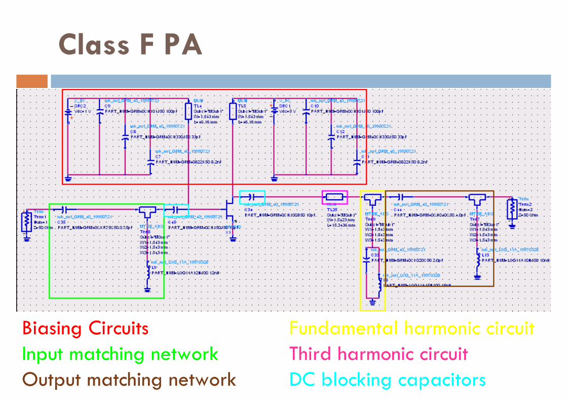
Class F PA
Biasing Circuits Fundamental harmonic circuitInput matching network Third harmonic circuitOutput matching network DC blocking capacitors
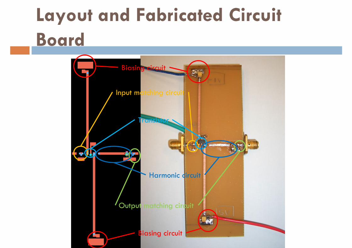
Layout and Fabricated Circuit Board
Biasing circuit
Biasing circuit
Output matching circuit
Input matching circuit
Transistor
Harmonic circuit
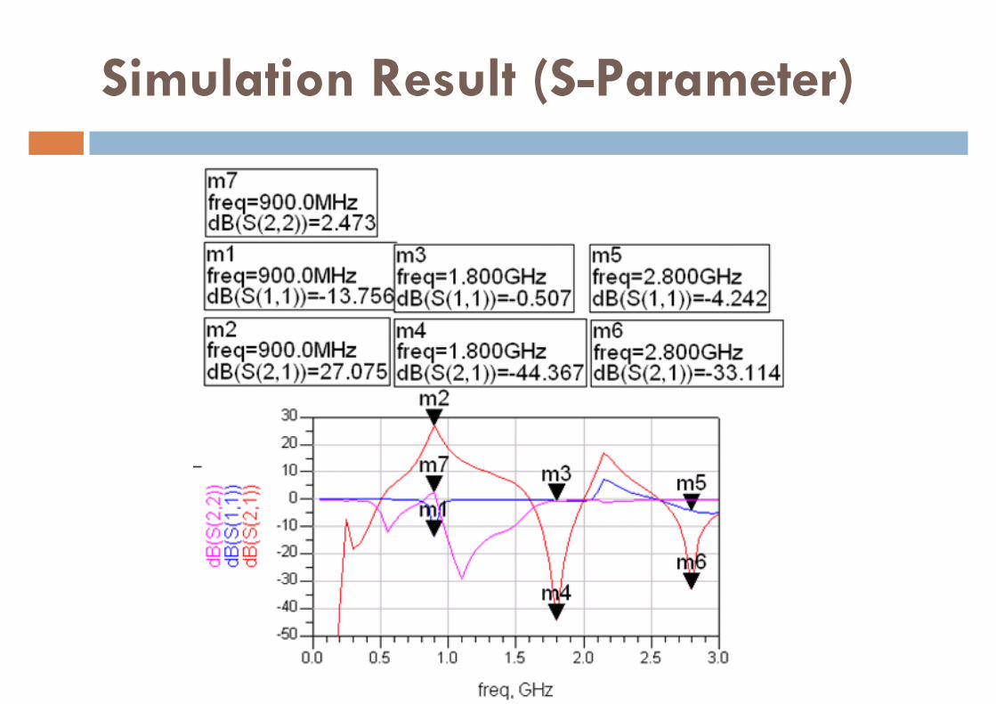
Simulation Result (S-Parameter)
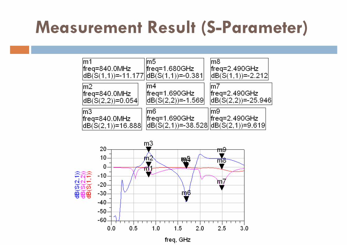
Measurement Result (S-Parameter)
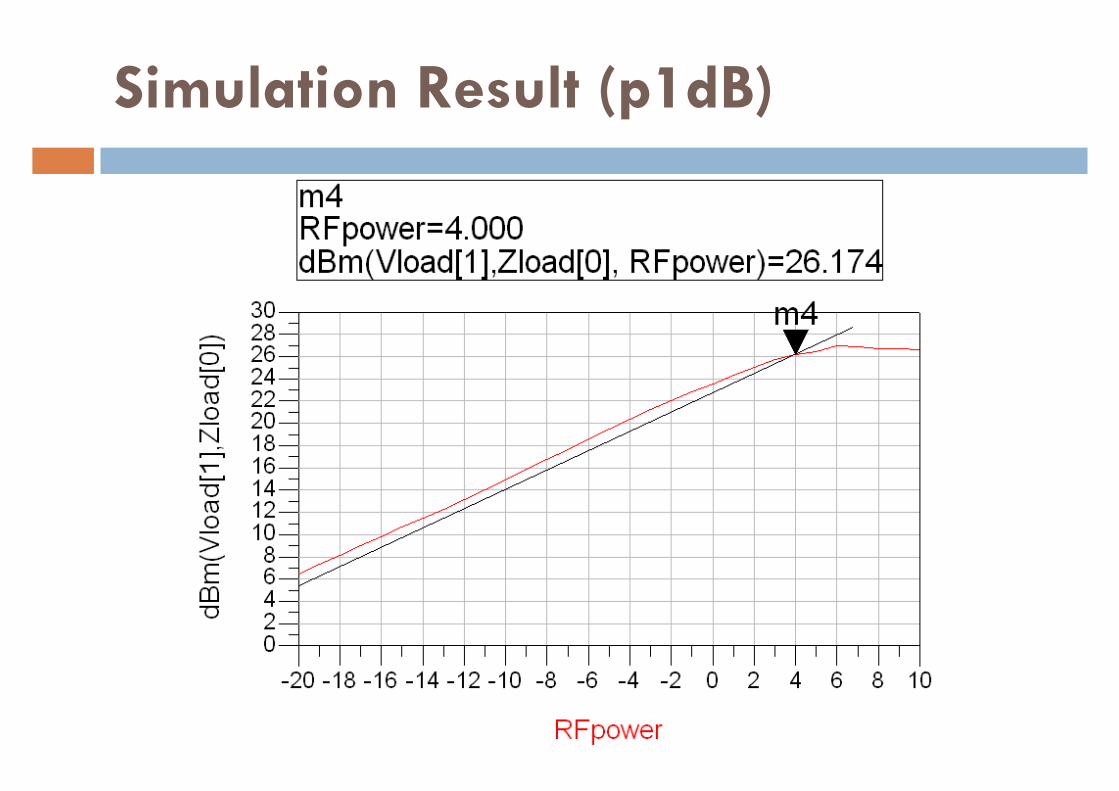
Simulation Result (p1dB)
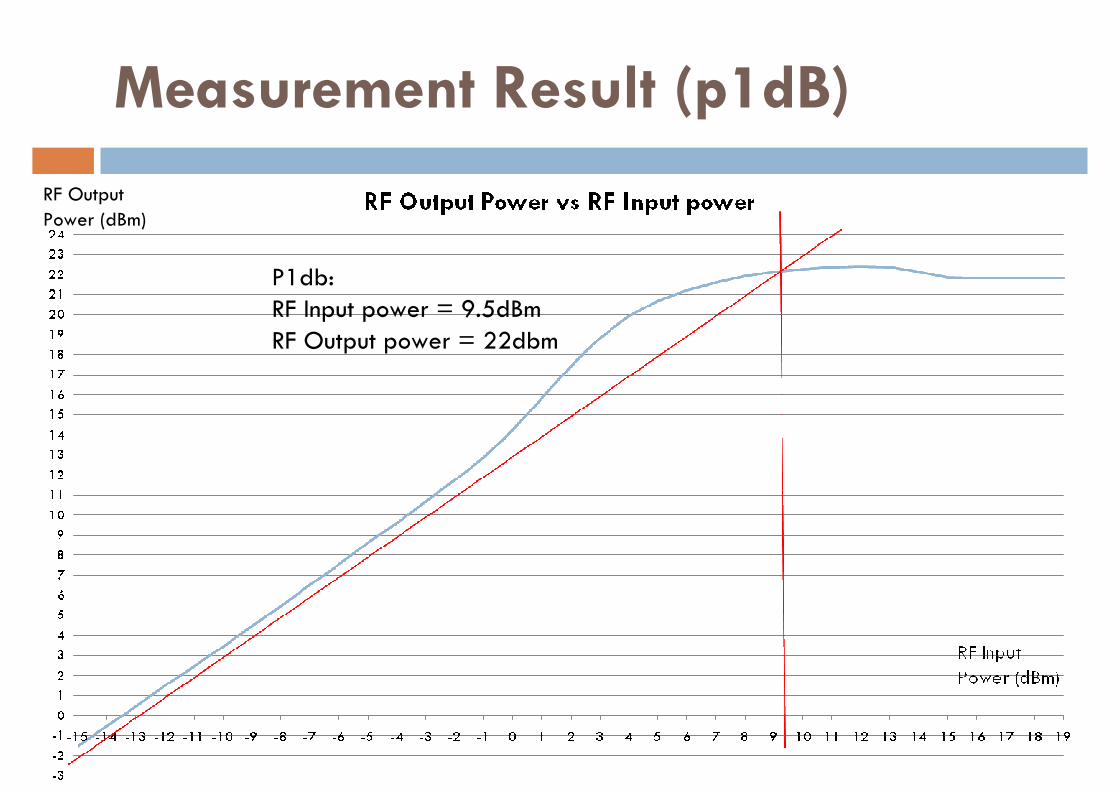
Measurement Result (p1dB)
RF Output Power (dBm)
P1db:RF Input power = 9.5dBmRF Output power = 22dbm

Simulation Result (PAE)
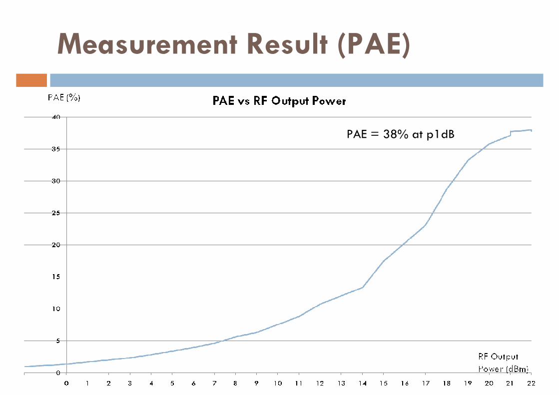
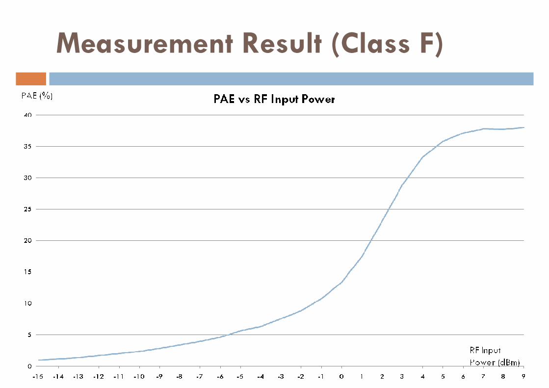
Measurement Result (PAE)
PAE = 38% at p1dB

END
Thank You

Q & A
Measurement Result (p1dB)
Measurement Result (Class B)
PAE (%)
Measurement Result (Class B + HTT)
PAE (%)
Measurement Result (Class F)