Embed Size (px)
DESCRIPTION
Instructor: Dr. Mohammad S. Hashmi
Citation preview

7/21/2019 RF Circuit Design (ECE321/521)-Lect_4_2014
http://slidepdf.com/reader/full/rf-circuit-design-ece321521-lect42014 1/40
Indraprastha Institute of
Information Technology Delhi ECE321/521
Lecture-4 Date: 14.08.2014
• Review – Lecture 3
• Terminated Lossless Transmission Line
• TL Input Impedance• Solved Examples
7/21/2019 RF Circuit Design (ECE321/521)-Lect_4_2014
http://slidepdf.com/reader/full/rf-circuit-design-ece321521-lect42014 2/40
Indraprastha Institute of
Information Technology Delhi ECE321/521
Z L
() L I
Z 0 L
I ( )V z
L I
L I
z
z = - l z =0
• For a terminated lossless transmission line, the current and voltage along
the line is:
0 0( ) j z j z V z V e e 0
0
0
( ) j z j z V I z e e
Z
Review – Lecture 3
7/21/2019 RF Circuit Design (ECE321/521)-Lect_4_2014
http://slidepdf.com/reader/full/rf-circuit-design-ece321521-lect42014 3/40
Indraprastha Institute of
Information Technology Delhi ECE321/521
Special Termination Conditions
• Let us consider a generic TL terminated in arbitrary impedance ZL
Z L
z = 0 z = -l
Z in 0
Z 0V(z)
I(z)
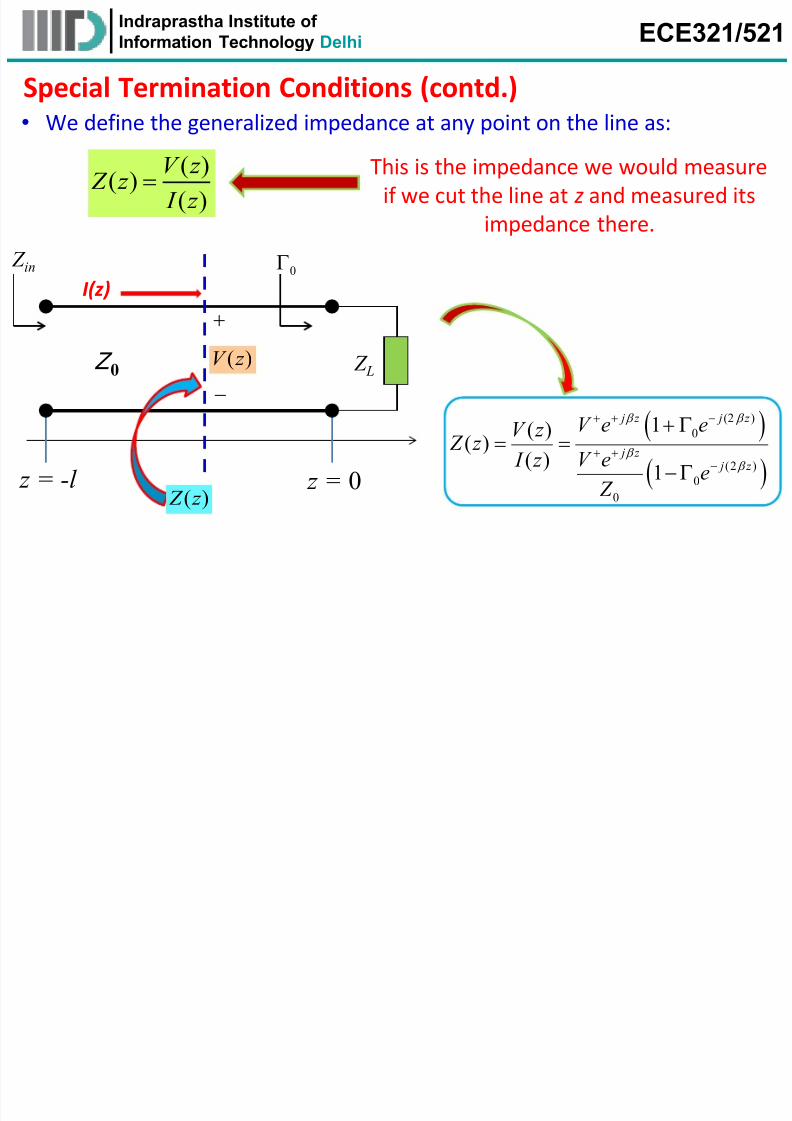
It’s interesting to note that the load ZL enforces a boundary
condition that explicitly determines neither V(z) nor I(z)—but
completely specifies line impedance Z(z)!
7/21/2019 RF Circuit Design (ECE321/521)-Lect_4_2014
http://slidepdf.com/reader/full/rf-circuit-design-ece321521-lect42014 4/40
Indraprastha Institute of
Information Technology Delhi ECE321/521
Special Termination Conditions (contd.)
z = 0
Z L
z = -l
Z in 0
Z 0
I(z)
( )V z
( ) Z z
• We define the generalized impedance at any point on the line as:
( )( )
( )
V z Z z
I z
This is the impedance we would measure
if we cut the line at z and measured its
impedance there.
(2 )
0
(2 )
0
0
1( )( )
( )1
j z j z
j z j z
V e eV z Z z
V e I z e
Z
7/21/2019 RF Circuit Design (ECE321/521)-Lect_4_2014
http://slidepdf.com/reader/full/rf-circuit-design-ece321521-lect42014 5/40
Indraprastha Institute of
Information Technology Delhi ECE321/521
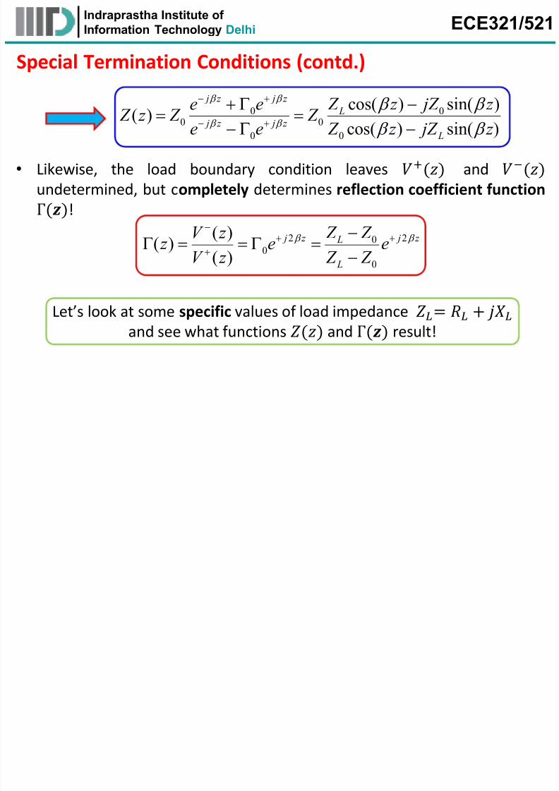
Special Termination Conditions (contd.)
2 200
0
( )( )
( )
j z j z L
L
V z Z Z z e e
V z Z Z
• Likewise, the load boundary condition leaves +() and −()
undetermined, but completely determines reflection coefficient functionΓ()!
0 00 0
0 0
cos( ) sin( )( )
cos( ) sin( )
j z j z L
j z j z
L
e e Z z jZ z Z z Z Z
e e Z z jZ z
Let’s look at some specific values of load impedance =
and see what functions () and Γ() result!
7/21/2019 RF Circuit Design (ECE321/521)-Lect_4_2014
http://slidepdf.com/reader/full/rf-circuit-design-ece321521-lect42014 6/40
Indraprastha Institute of
Information Technology Delhi ECE321/521
Special Termination Conditions (contd.)
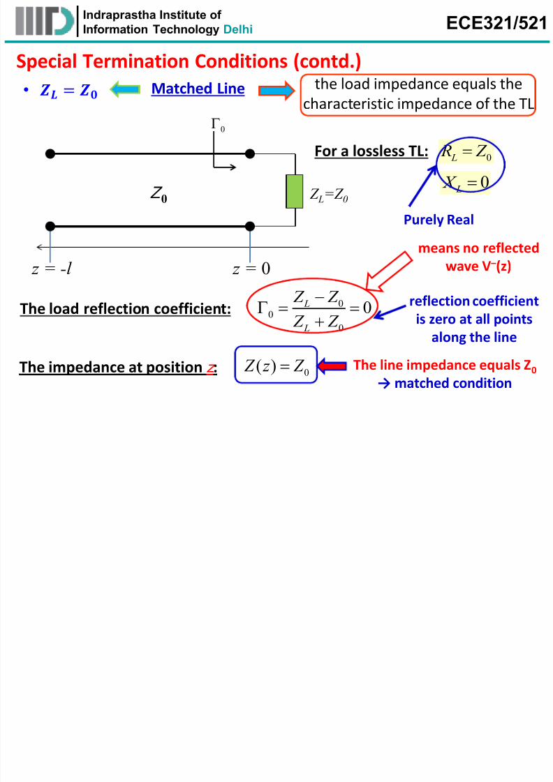
•
=
z = 0
Z L=Z 0
z = -l
0
Z 0
0 L R Z For a lossless TL:
0 L
X
00
0
0 L
L
Z Z
Z Z
The load reflection coefficient:
means no reflected
wave V –(z)
Purely Real
0( ) Z z Z The impedance at position z :
reflection coefficient
is zero at all points
along the line
The line impedance equals Z0
→ matched condition
Matched Line
the load impedance equals the
characteristic impedance of the TL
7/21/2019 RF Circuit Design (ECE321/521)-Lect_4_2014
http://slidepdf.com/reader/full/rf-circuit-design-ece321521-lect42014 7/40
Indraprastha Institute of
Information Technology Delhi ECE321/521
Special Termination Conditions (contd.)
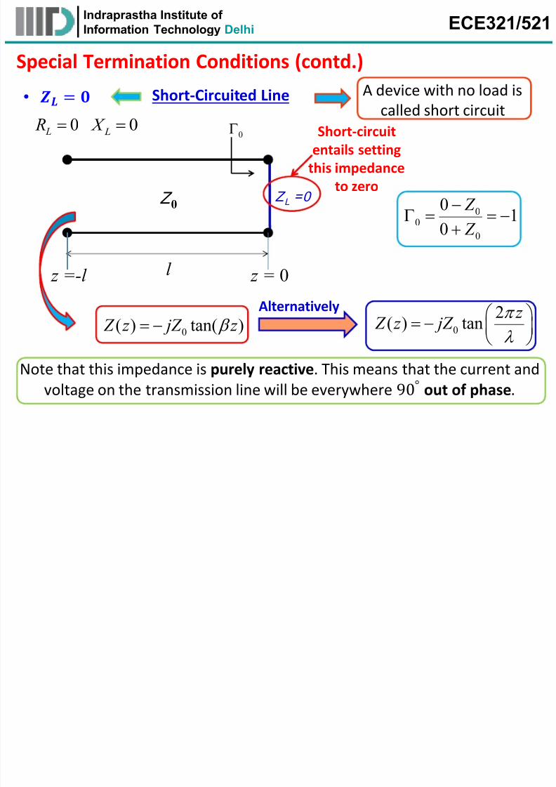
• = Short-Circuited Line A device with no load iscalled short circuit
Z L =0
z = 0 z =-l
0
Z 0
l
0( ) tan( ) Z z jZ z
Short-circuit
entails setting
this impedance
to zero
Alternatively
0
2( ) tan
z Z z jZ
0 L R 0 L X
00
0
01
0
Z
Z
Note that this impedance is purely reactive. This means that the current and
voltage on the transmission line will be everywhere 90° out of phase.
7/21/2019 RF Circuit Design (ECE321/521)-Lect_4_2014
http://slidepdf.com/reader/full/rf-circuit-design-ece321521-lect42014 8/40
Indraprastha Institute of
Information Technology Delhi ECE321/521
Special Termination Conditions (contd.)
0 0( ) 2 sin( ) j z j z V z V e e j V z 0
0
2( ) cos( )
V I z z
Z
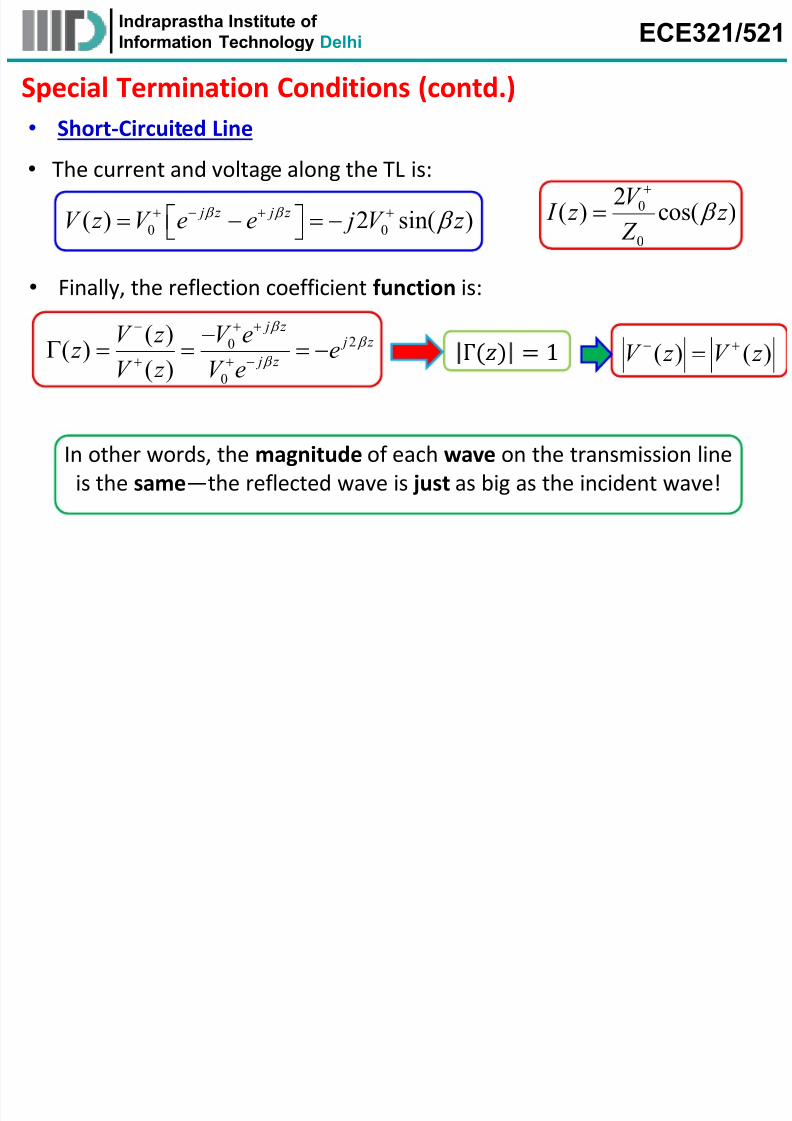
• The current and voltage along the TL is:
• Finally, the reflection coefficient function is:
•
Short-Circuited Line
20
0
( )( )
( )
j z j z
j z
V z V e z e
V z V e
Γ() = 1 ( ) ( )V z V z
In other words, the magnitude of each wave on the transmission line
is the same—the reflected wave is just as big as the incident wave!
7/21/2019 RF Circuit Design (ECE321/521)-Lect_4_2014
http://slidepdf.com/reader/full/rf-circuit-design-ece321521-lect42014 9/40
Indraprastha Institute of
Information Technology Delhi ECE321/521
Special Termination Conditions (contd.)
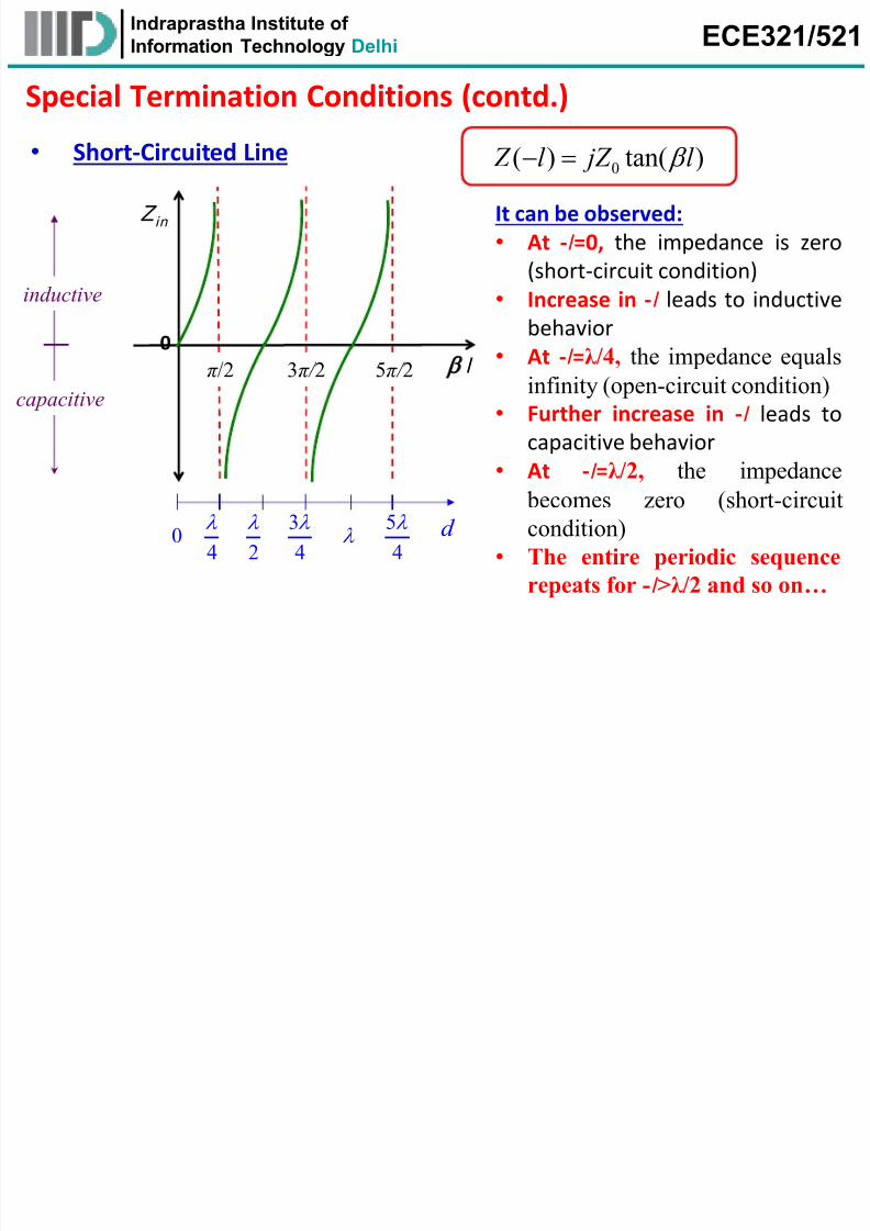
• Short-Circuited Line 0( ) tan( ) Z l jZ l
Z in
lπ /2 3π / 2
inductive
capacitive
5π / 2
3 50
4 2 4 4
d
0
It can be observed:
• At -l =0, the impedance is zero
(short-circuit condition)
•Increase in -l leads to inductivebehavior
• At -l =λ /4, the impedance equals
infinity (open-circuit condition)
• Further increase in -l leads to
capacitive behavior• At -l =λ /2, the impedance
becomes zero (short-circuit
condition)
• The entire periodic sequence
repeats for -l >λ /2 and so on…
7/21/2019 RF Circuit Design (ECE321/521)-Lect_4_2014
http://slidepdf.com/reader/full/rf-circuit-design-ece321521-lect42014 10/40
Indraprastha Institute of
Information Technology Delhi ECE321/521
Special Termination Conditions (contd.)
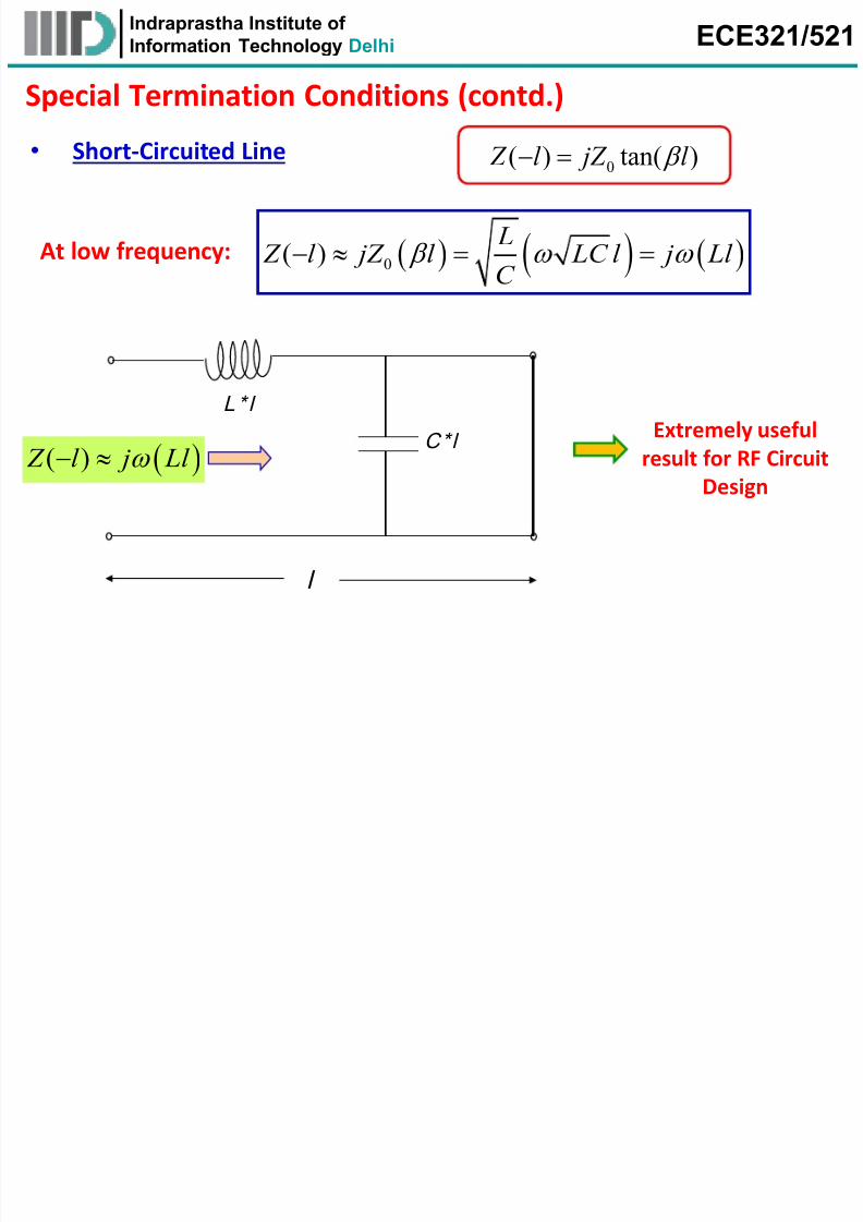
• Short-Circuited Line
At low frequency: 0( ) L
Z l jZ l LC l j Ll C
( ) Z l j Ll
L* l
l
C*l
Extremely useful
result for RF Circuit
Design
0( ) tan( ) Z l jZ l
7/21/2019 RF Circuit Design (ECE321/521)-Lect_4_2014
http://slidepdf.com/reader/full/rf-circuit-design-ece321521-lect42014 11/40
Indraprastha Institute of
Information Technology Delhi ECE321/521
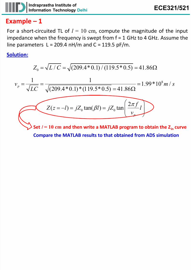
Example – 1
For a short-circuited TL of l = 10 cm, compute the magnitude of the inputimpedance when the frequency is swept from f = 1 GHz to 4 GHz. Assume the
line parameters L = 209.4 nH/m and C = 119.5 pF/m.
Solution:
0 / (209.4* 0.1) / (119.5* 0.5) 41.86 Z L C
81 11.99 *10 /
(209.4 * 0.1) * (119.5* 0.5) 41.86 pv m s
LC
0 0
2( ) tan( ) tan
p
f Z z l jZ l jZ l
v
Set l = 10 cm and then write a MATLAB program to obtain the Zin curve
Compare the MATLAB results to that obtained from ADS simulation
7/21/2019 RF Circuit Design (ECE321/521)-Lect_4_2014
http://slidepdf.com/reader/full/rf-circuit-design-ece321521-lect42014 12/40
Indraprastha Institute of
Information Technology Delhi ECE321/521
Special Termination Conditions (contd.)
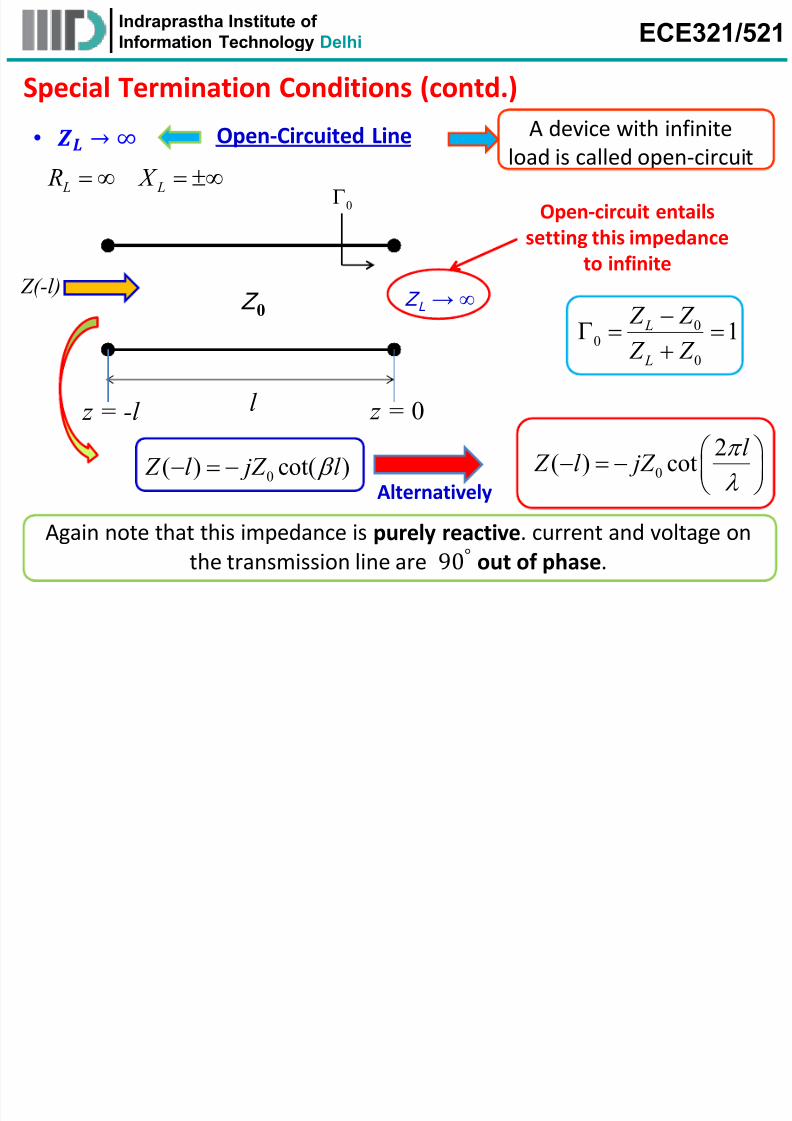
• → ∞ Open-Circuited Line A device with infiniteload is called open-circuit
L R L X
Z L → ∞
z = 0 z = -l
Z(-l)
0
Z 0
l
0( ) cot( ) Z l jZ l
Open-circuit entails
setting this impedance
to infinite
Alternatively0
2( ) cot
l Z l jZ
00
0
1 L
L
Z Z
Z Z
Again note that this impedance is purely reactive. current and voltage on
the transmission line are 90° out of phase.
7/21/2019 RF Circuit Design (ECE321/521)-Lect_4_2014
http://slidepdf.com/reader/full/rf-circuit-design-ece321521-lect42014 13/40
Indraprastha Institute of
Information Technology Delhi ECE321/521
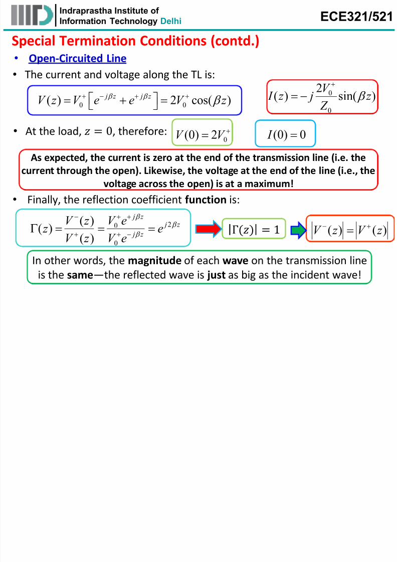
0 0( ) 2 cos( ) j z j z V z V e e V z 0
0
2( ) sin( )
V I z j z
Z
• The current and voltage along the TL is:
• Open-Circuited Line
• Finally, the reflection coefficient function is:
20
0
( )( )
( )
j z j z
j z
V z V e z e
V z V e
Γ() = 1 ( ) ( )V z V z
In other words, the magnitude of each wave on the transmission line
is the same—the reflected wave is just as big as the incident wave!
Special Termination Conditions (contd.)
• At the load, = 0, therefore:0(0) 2V V
(0) 0 I As expected, the current is zero at the end of the transmission line (i.e. the
current through the open). Likewise, the voltage at the end of the line (i.e., the
voltage across the open) is at a maximum!
7/21/2019 RF Circuit Design (ECE321/521)-Lect_4_2014
http://slidepdf.com/reader/full/rf-circuit-design-ece321521-lect42014 14/40
Indraprastha Institute of
Information Technology Delhi ECE321/521
Special Termination Conditions (contd.)
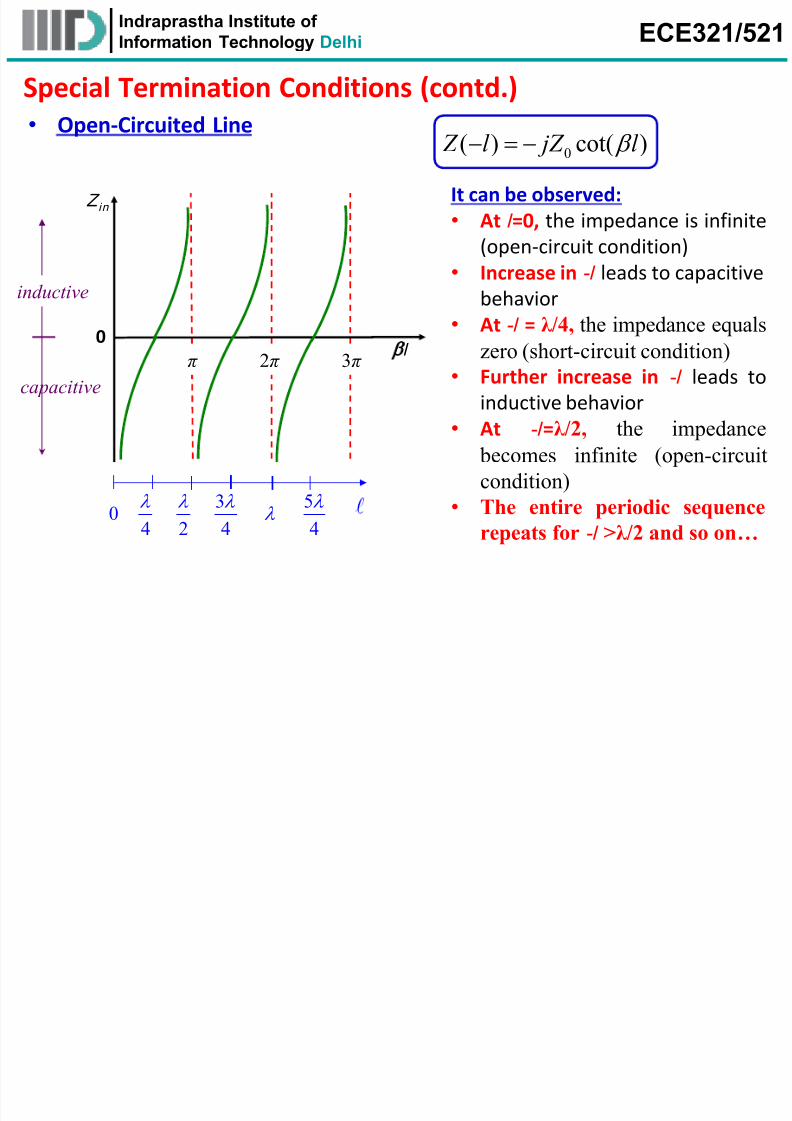
0( ) cot( ) Z l jZ l
It can be observed:
• At l =0, the impedance is infinite
(open-circuit condition)
•Increase in -l leads to capacitivebehavior
• At -l = λ /4, the impedance equals
zero (short-circuit condition)
• Further increase in -l leads to
inductive behavior• At -l =λ /2, the impedance
becomes infinite (open-circuit
condition)
• The entire periodic sequence
repeats for -l >λ /2 and so on…
Z in
π 2π 3π
inductive
capacitive
l
3 50
4 2 4 4
0
• Open-Circuited Line
7/21/2019 RF Circuit Design (ECE321/521)-Lect_4_2014
http://slidepdf.com/reader/full/rf-circuit-design-ece321521-lect42014 15/40
Indraprastha Institute of
Information Technology Delhi ECE321/521
Special Termination Conditions (contd.)
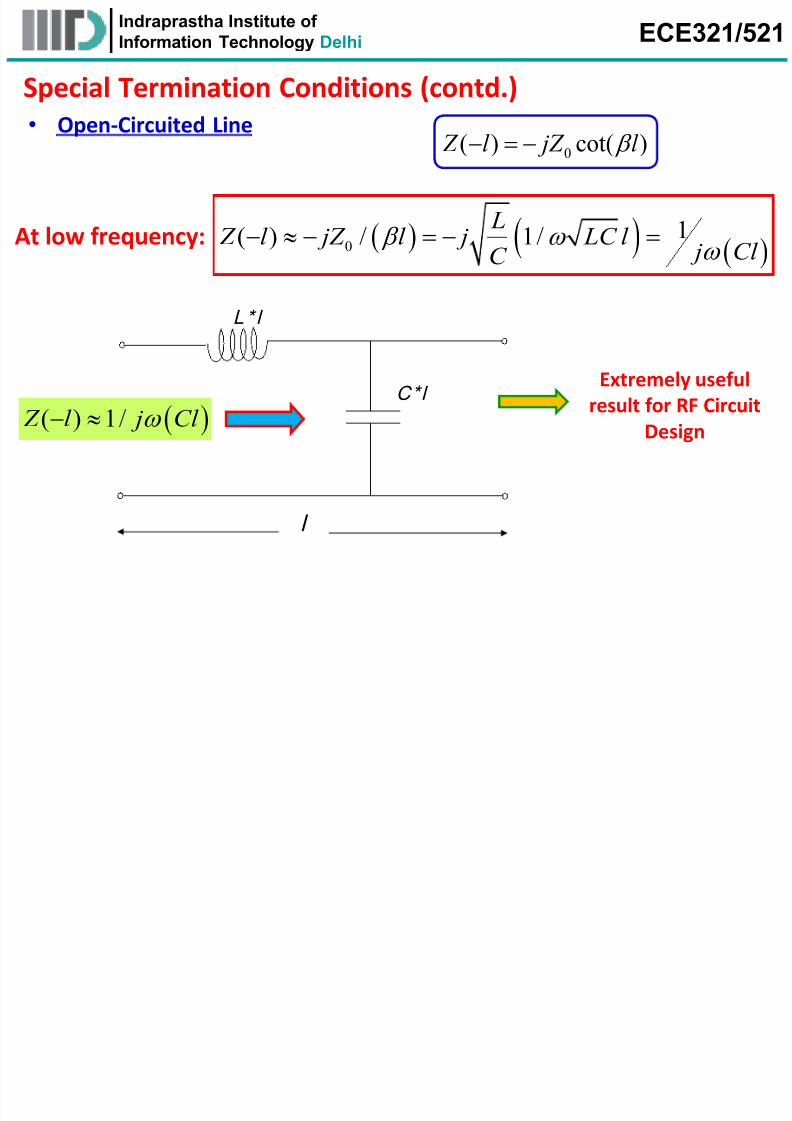
0( ) cot( ) Z l jZ l • Open-Circuited Line
At low frequency: 01( ) / 1/
L Z l jZ l j LC l
j Cl C
Extremely useful
result for RF CircuitDesign
L* l
l
C*l
( ) 1/ Z l j Cl
7/21/2019 RF Circuit Design (ECE321/521)-Lect_4_2014
http://slidepdf.com/reader/full/rf-circuit-design-ece321521-lect42014 16/40
Indraprastha Institute of
Information Technology Delhi ECE321/521
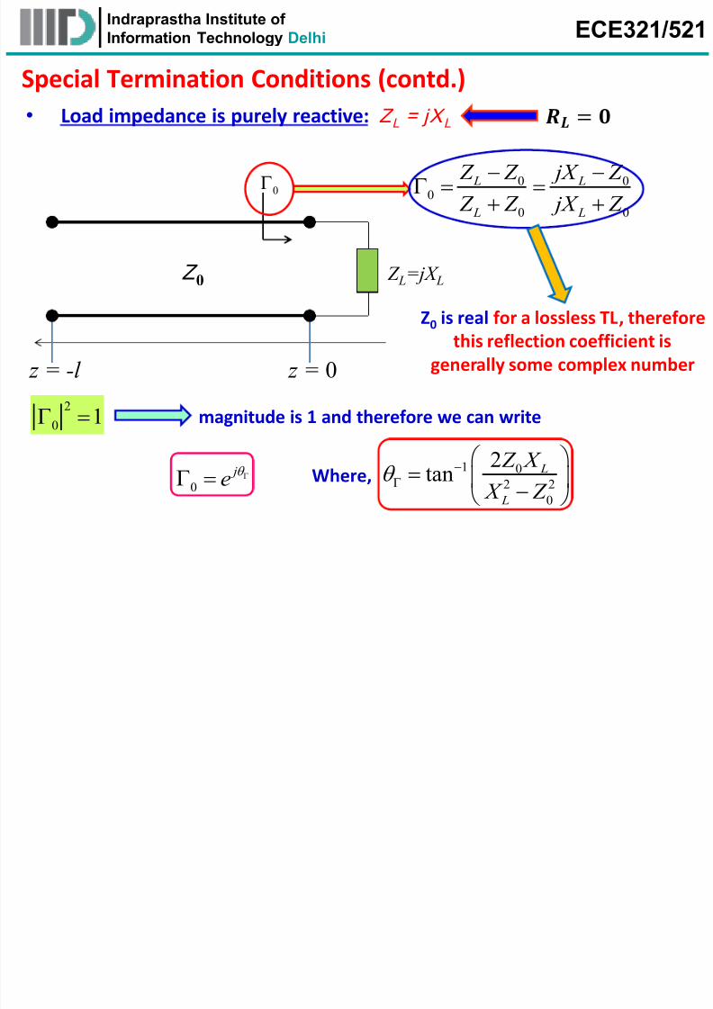
•
Load impedance is purely reactive: Z L = jX L
z = 0
Z L=jX L
z = -l
0
Z 0
0 00
0 0
L L
L L
Z Z jX Z
Z Z jX Z
Z0 is real for a lossless TL, therefore
this reflection coefficient is
generally some complex number
2
0 1 magnitude is 1 and therefore we can write
0
je
Where,1 0
2 2
0
2tan L
L
Z X
X Z
Special Termination Conditions (contd.)
=
7/21/2019 RF Circuit Design (ECE321/521)-Lect_4_2014
http://slidepdf.com/reader/full/rf-circuit-design-ece321521-lect42014 17/40
Indraprastha Institute of
Information Technology Delhi ECE321/521
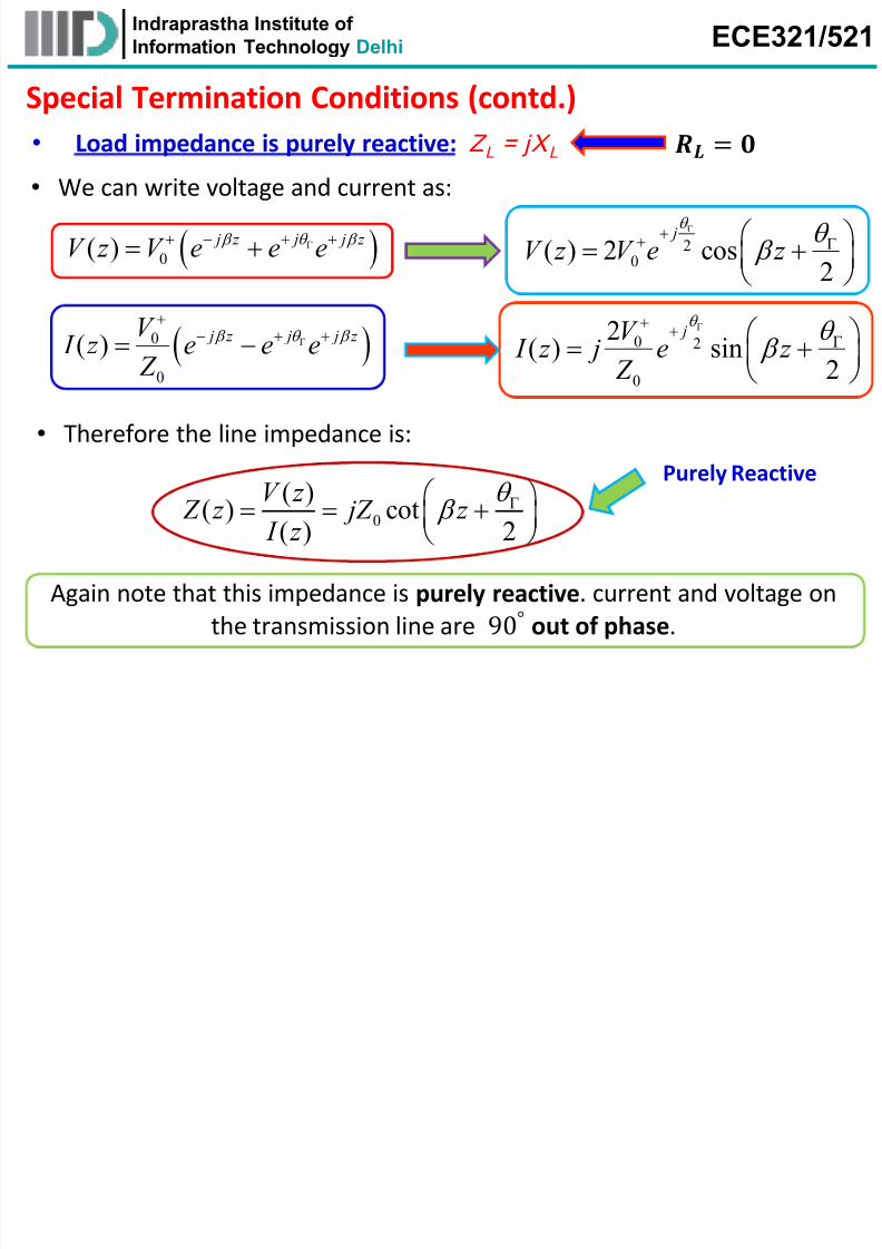
• We can write voltage and current as:
0( ) j j z j z V z V e e e
0
0
( ) j j z j z V I z e e e
Z
• Therefore the line impedance is:
0
( )( ) cot
( ) 2
V z Z z jZ z
I z
Purely Reactive
•
Load impedance is purely reactive: Z L = jX L
Special Termination Conditions (contd.)
=
20( ) 2 cos
2
j
V z V e z
0 2
0
2( ) sin
2
jV I z j e z
Z
Again note that this impedance is purely reactive. current and voltage on
the transmission line are 90° out of phase.
7/21/2019 RF Circuit Design (ECE321/521)-Lect_4_2014
http://slidepdf.com/reader/full/rf-circuit-design-ece321521-lect42014 18/40
Indraprastha Institute of
Information Technology Delhi ECE321/521
•
Load impedance is purely reactive: Z L = jX L
Special Termination Conditions (contd.)
=
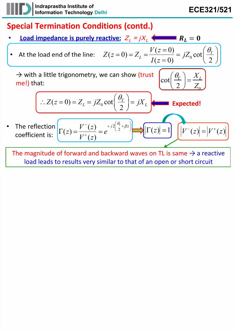
→ with a little trigonometry, we can show (trust
me!) that:0
cot 2
L X
Z
0( 0) cot2
L L Z z Z jZ jX
Expected!
• The reflection
coefficient is:
22( )
( )( )
j z V z z e
V z
( ) 1 z
The magnitude of forward and backward waves on TL is same → a reactive
load leads to results very similar to that of an open or short circuit
0
( 0)( 0) cot
( 0) 2 L
V z Z z Z jZ
I z
• At the load end of the line:
( ) ( )V z V z
7/21/2019 RF Circuit Design (ECE321/521)-Lect_4_2014
http://slidepdf.com/reader/full/rf-circuit-design-ece321521-lect42014 19/40
Indraprastha Institute of
Information Technology Delhi ECE321/521
Special Termination Conditions (contd.)
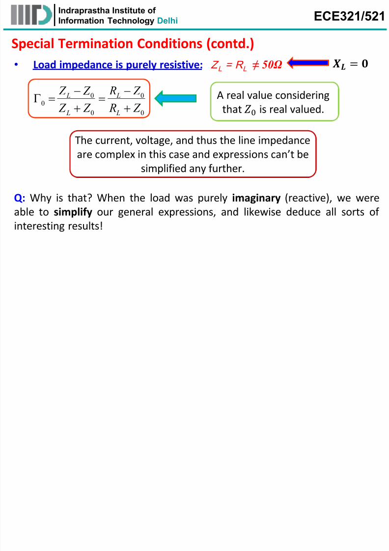
•
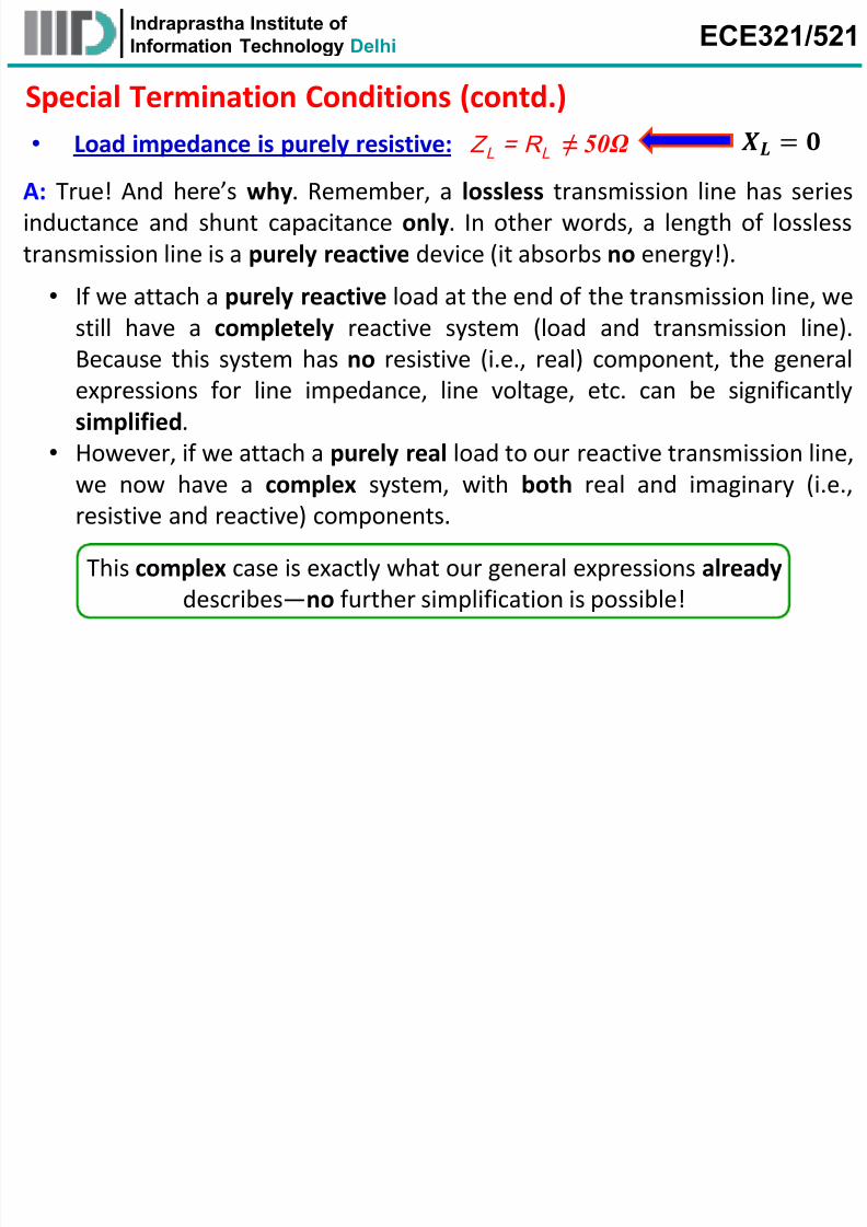
Load impedance is purely resistive: Z L = R L ≠ 50Ω =
0 00
0 0
L L
L L
Z Z R Z
Z Z R Z
A real value considering
that is real valued.
The current, voltage, and thus the line impedance
are complex in this case and expressions can’t be
simplified any further.
Q: Why is that? When the load was purely imaginary (reactive), we wereable to simplify our general expressions, and likewise deduce all sorts of
interesting results!
7/21/2019 RF Circuit Design (ECE321/521)-Lect_4_2014
http://slidepdf.com/reader/full/rf-circuit-design-ece321521-lect42014 20/40
Indraprastha Institute of
Information Technology Delhi ECE321/521
Special Termination Conditions (contd.)
•
Load impedance is purely resistive: Z L = R L ≠ 50Ω = A: True! And here’s why. Remember, a lossless transmission line has series
inductance and shunt capacitance only. In other words, a length of lossless
transmission line is a purely reactive device (it absorbs no energy!).
•
If we attach a purely reactive load at the end of the transmission line, westill have a completely reactive system (load and transmission line).
Because this system has no resistive (i.e., real) component, the general
expressions for line impedance, line voltage, etc. can be significantly
simplified.
• However, if we attach a purely real load to our reactive transmission line,we now have a complex system, with both real and imaginary (i.e.,
resistive and reactive) components.
This complex case is exactly what our general expressions already
describes—no further simplification is possible!
7/21/2019 RF Circuit Design (ECE321/521)-Lect_4_2014
http://slidepdf.com/reader/full/rf-circuit-design-ece321521-lect42014 21/40
Indraprastha Institute of
Information Technology Delhi ECE321/521
Special Termination Conditions (contd.)
•
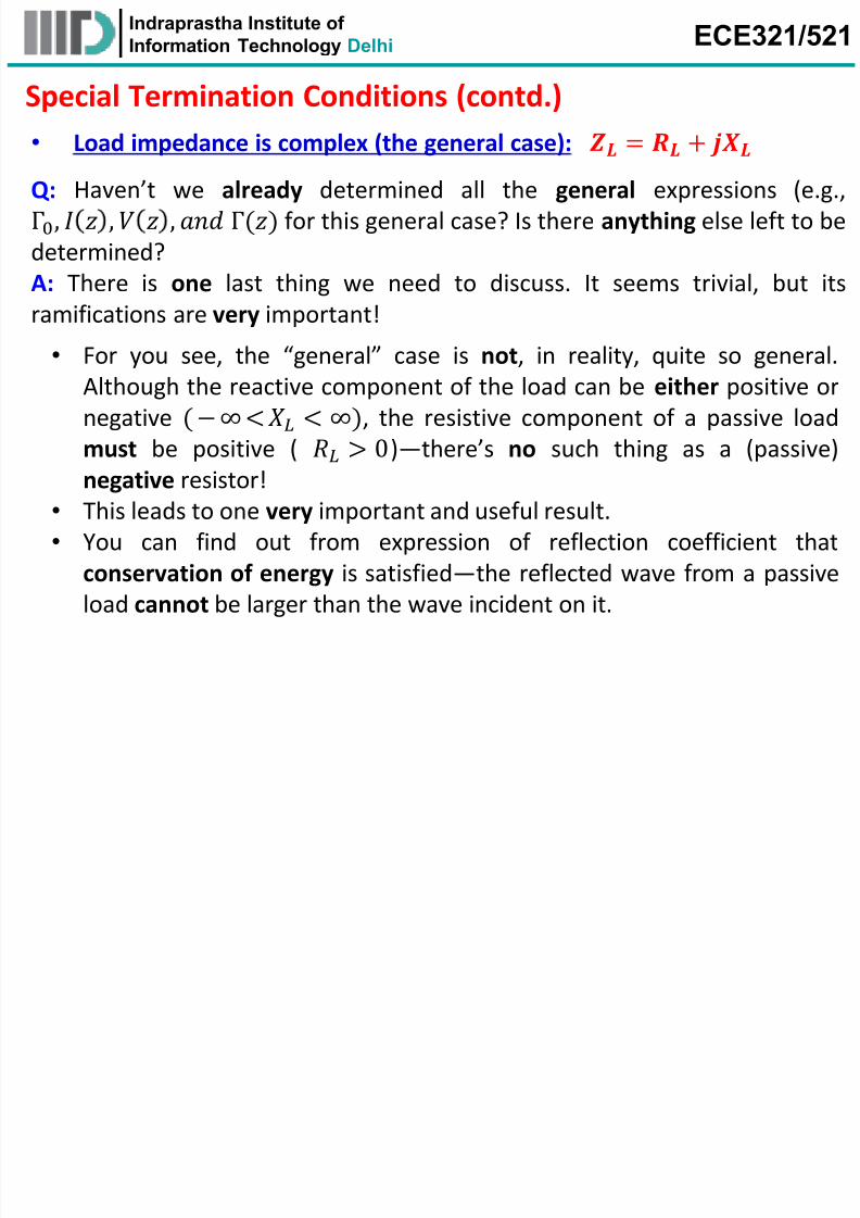
Load impedance is complex (the general case): =
Q: Haven’t we already determined all the general expressions (e.g.,
Γ, , , Γ() for this general case? Is there anything else left to be
determined?
A: There is one last thing we need to discuss. It seems trivial, but its
ramifications are very important!
• For you see, the “general” case is not, in reality, quite so general.
Although the reactive component of the load can be either positive or
negative ( ∞ < < ∞), the resistive component of a passive load
must be positive ( > 0)—there’s no such thing as a (passive)negative resistor!
• This leads to one very important and useful result.
• You can find out from expression of reflection coefficient that
conservation of energy is satisfied—the reflected wave from a passive
load cannot be larger than the wave incident on it.
7/21/2019 RF Circuit Design (ECE321/521)-Lect_4_2014
http://slidepdf.com/reader/full/rf-circuit-design-ece321521-lect42014 22/40
Indraprastha Institute of
Information Technology Delhi ECE321/521
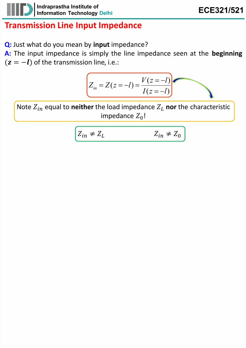
Transmission Line Input Impedance
Q: Just what do you mean by input impedance?A: The input impedance is simply the line impedance seen at the beginning
( = ) of the transmission line, i.e.:
( )
( ) ( )in
V z l
Z Z z l I z l
Note equal to neither the load impedance nor the characteristic
impedance !
≠ ≠
f
7/21/2019 RF Circuit Design (ECE321/521)-Lect_4_2014
http://slidepdf.com/reader/full/rf-circuit-design-ece321521-lect42014 23/40
Indraprastha Institute of
Information Technology Delhi ECE321/521
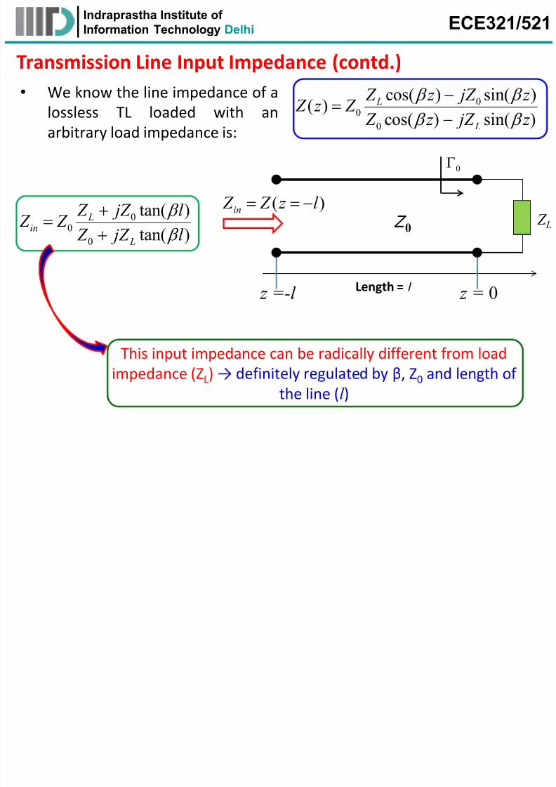
Transmission Line Input Impedance (contd.)
•
We know the line impedance of alossless TL loaded with an
arbitrary load impedance is:
00
0
cos( ) sin( )( )cos( ) sin( )
L
L
Z z jZ z Z z Z Z z jZ z
z = 0
Z L
z =-l
0
Z 0
Length = l
( )in Z Z z l 0
0
0
tan( )
tan( ) L
in
L
Z jZ l Z Z
Z jZ l
This input impedance can be radically different from load
impedance (ZL) → definitely regulated by β, Z0 and length of
the line (l )
I d th I tit t f

7/21/2019 RF Circuit Design (ECE321/521)-Lect_4_2014
http://slidepdf.com/reader/full/rf-circuit-design-ece321521-lect42014 24/40
Indraprastha Institute of
Information Technology Delhi ECE321/521
Transmission Line Input Impedance – Special Cases
•
Now let us look at the input impedances for some important loadimpedances and line lengths
→ You should commit these
results to memory
I d th I tit t f
7/21/2019 RF Circuit Design (ECE321/521)-Lect_4_2014
http://slidepdf.com/reader/full/rf-circuit-design-ece321521-lect42014 25/40
Indraprastha Institute of
Information Technology Delhi ECE321/521
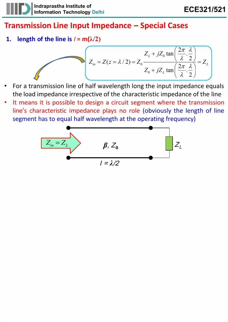
1. length of the line is l = m(λ /2)
• For a transmission line of half wavelength long the input impedance equals
the load impedance irrespective of the characteristic impedance of the line
• It means it is possible to design a circuit segment where the transmission
line’s characteristic impedance plays no role (obviously the length of line
segment has to equal half wavelength at the operating frequency)
Transmission Line Input Impedance – Special Cases
Z L β , Z 0
l = λ /2
in L Z Z
0
0
0
2tan .
2( / 2)
2tan .
2
L
in L
L
Z jZ
Z Z z Z Z
Z jZ
I d th I tit t f
7/21/2019 RF Circuit Design (ECE321/521)-Lect_4_2014
http://slidepdf.com/reader/full/rf-circuit-design-ece321521-lect42014 26/40
Indraprastha Institute of
Information Technology Delhi ECE321/521
Transmission Line Input Impedance – Special Cases (contd.)
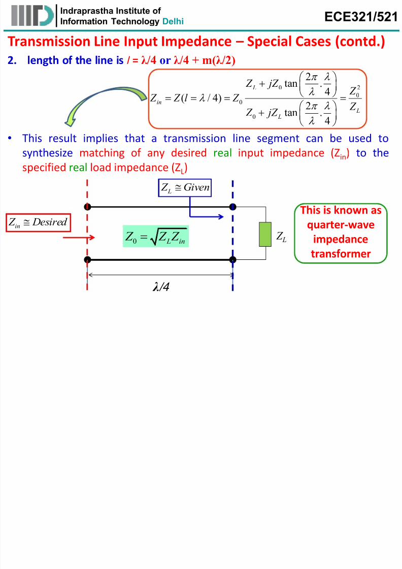
2. length of the line is l = λ /4 or λ /4 + m(λ /2)
•
This result implies that a transmission line segment can be used tosynthesize matching of any desired real input impedance (Zin) to the
specified real load impedance (ZL)
λ /4
Z L
L Z Given
in Z Desired
0 L in Z Z Z
This is known asquarter-wave
impedance
transformer
20
00
0
2tan .
4( / 4)
2tan .
4
L
in
L L
Z jZ Z
Z Z l Z Z
Z jZ
I d th I tit t f
7/21/2019 RF Circuit Design (ECE321/521)-Lect_4_2014
http://slidepdf.com/reader/full/rf-circuit-design-ece321521-lect42014 27/40
Indraprastha Institute of
Information Technology Delhi ECE321/521
Z L=0 β , Z 0
l = λ /4
in Z
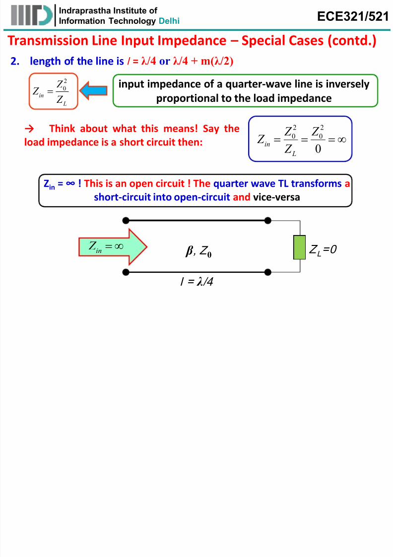
2. length of the line is l = λ /4 or λ /4 + m(λ /2)
Transmission Line Input Impedance – Special Cases (contd.)
Zin = ∞ ! This is an open circuit ! The quarter wave TL transforms a
short-circuit into open-circuit and vice-versa
2
0in
L
Z Z
Z
input impedance of a quarter-wave line is inversely
proportional to the load impedance
→ Think about what this means! Say the
load impedance is a short circuit then:
2 2
0 0
0in
L
Z Z Z
Z
Indraprastha Institute of
7/21/2019 RF Circuit Design (ECE321/521)-Lect_4_2014
http://slidepdf.com/reader/full/rf-circuit-design-ece321521-lect42014 28/40
Indraprastha Institute of
Information Technology Delhi ECE321/521
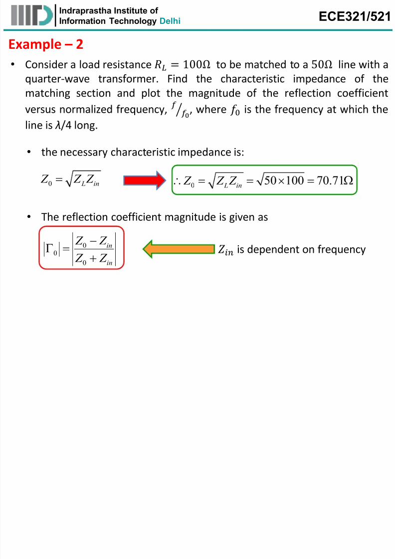
• Consider a load resistance = 100Ω
to be matched to a50Ω
line with a
quarter-wave transformer. Find the characteristic impedance of the
matching section and plot the magnitude of the reflection coefficient
versus normalized frequency,
, where is the frequency at which the
line is λ/4 long.
Example – 2
• the necessary characteristic impedance is:
0 L in Z Z Z
0 50 100 70.71 L in
Z Z Z
is dependent on frequency
• The reflection coefficient magnitude is given as
00
0
in
in
Z Z
Z Z
Indraprastha Institute of
7/21/2019 RF Circuit Design (ECE321/521)-Lect_4_2014
http://slidepdf.com/reader/full/rf-circuit-design-ece321521-lect42014 29/40
Indraprastha Institute of
Information Technology Delhi ECE321/521
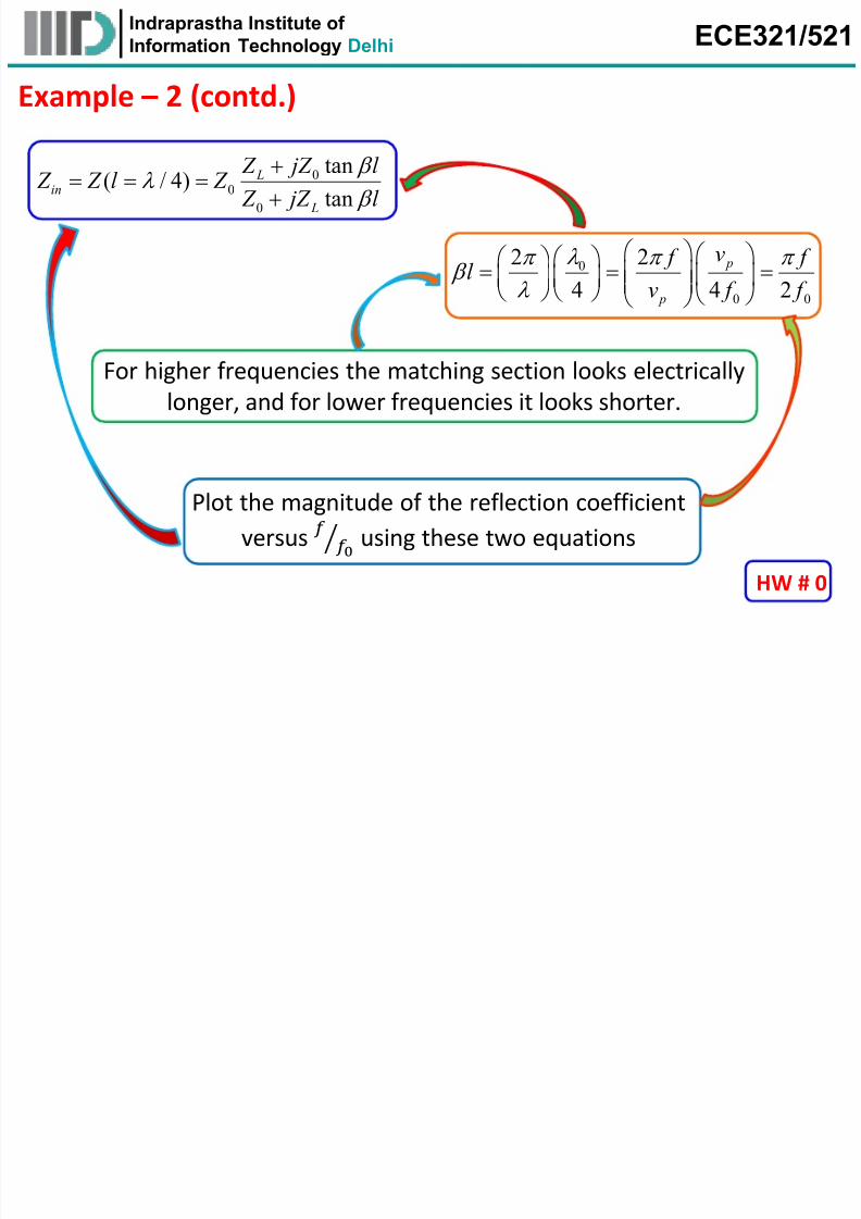
Example – 2 (contd.)
00
0
tan( / 4)
tan
Lin
L
Z jZ l Z Z l Z
Z jZ l
0
0 0
2 2
4 4 2
p
p
v f f l
v f f
For higher frequencies the matching section looks electrically
longer, and for lower frequencies it looks shorter.
Plot the magnitude of the reflection coefficient
versus
using these two equations
HW # 0
Indraprastha Institute of
7/21/2019 RF Circuit Design (ECE321/521)-Lect_4_2014
http://slidepdf.com/reader/full/rf-circuit-design-ece321521-lect42014 30/40
Indraprastha Institute of
Information Technology Delhi ECE321/521
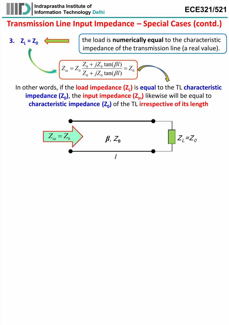
Transmission Line Input Impedance – Special Cases (contd.)
3. ZL = Z0
In other words, if the load impedance (ZL) is equal to the TL characteristic
impedance (Z0), the input impedance (Zin) likewise will be equal to
characteristic impedance (Z0) of the TL irrespective of its length
Z L=Z 0 β , Z 0
l
0in Z Z
the load is numerically equal to the characteristicimpedance of the transmission line (a real value).
0 00 0
0 0
tan( )
tan( )in
Z jZ l Z Z Z
Z jZ l
Indraprastha Institute of
7/21/2019 RF Circuit Design (ECE321/521)-Lect_4_2014
http://slidepdf.com/reader/full/rf-circuit-design-ece321521-lect42014 31/40
Indraprastha Institute of
Information Technology Delhi ECE321/521
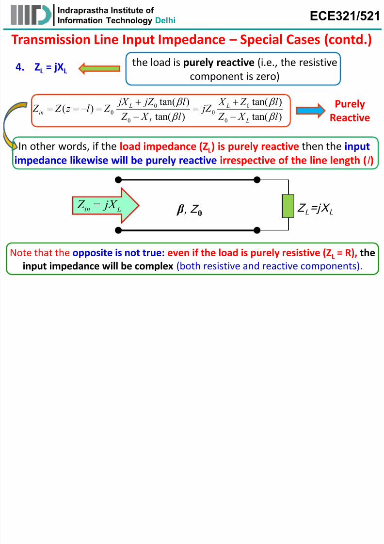
Transmission Line Input Impedance – Special Cases (contd.)
4. ZL = jXL
Z L=jX L β , Z 0in L Z jX
Note that the opposite is not true: even if the load is purely resistive (ZL = R), the
input impedance will be complex (both resistive and reactive components).
the load is purely reactive (i.e., the resistive
component is zero)
0 00 0
0 0
tan( ) tan( )( )
tan( ) tan( )
L Lin
L L
jX jZ l X Z l Z Z z l Z jZ
Z X l Z X l
Purely
Reactive
In other words, if the load impedance (ZL) is purely reactive then the input
impedance likewise will be purely reactive irrespective of the line length (l )
Indraprastha Institute of
7/21/2019 RF Circuit Design (ECE321/521)-Lect_4_2014
http://slidepdf.com/reader/full/rf-circuit-design-ece321521-lect42014 32/40
Indraprastha Institute of
Information Technology Delhi ECE321/521
Transmission Line Input Impedance – Special Cases (contd.)
4. ZL = jXL
Note that the opposite is not true: even if the load is purely
resistive ( = ), the input impedance will be complex (both
resistive and reactive components).
Q: Why is this?
A: ??
Indraprastha Institute of
7/21/2019 RF Circuit Design (ECE321/521)-Lect_4_2014
http://slidepdf.com/reader/full/rf-circuit-design-ece321521-lect42014 33/40
Indraprastha Institute of
Information Technology Delhi ECE321/521
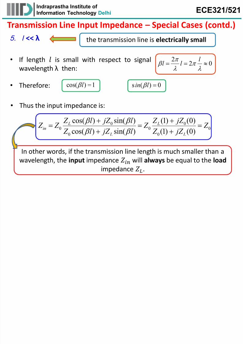
5. l << λ
Transmission Line Input Impedance – Special Cases (contd.)
the transmission line is electrically small
• If length is small with respect to signal
wavelength λ then:
22 0
l l l
• Therefore: cos( ) 1l s ( ) 0in l
• Thus the input impedance is:
0 0
0 0 00 0
cos( ) sin( ) (1) (0)
cos( ) sin( ) (1) (0)
L L
in L L
Z l jZ l Z jZ
Z Z Z Z Z l jZ l Z jZ
In other words, if the transmission line length is much smaller than a
wavelength, the input impedance will always be equal to the load
impedance .
Indraprastha Institute ofC /
7/21/2019 RF Circuit Design (ECE321/521)-Lect_4_2014
http://slidepdf.com/reader/full/rf-circuit-design-ece321521-lect42014 34/40
Indraprastha Institute of
Information Technology Delhi ECE321/521
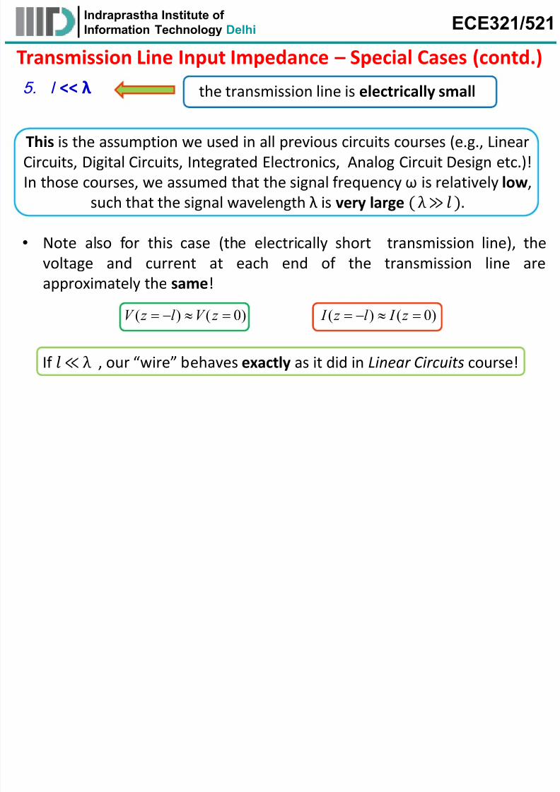
5. l << λ
Transmission Line Input Impedance – Special Cases (contd.)
the transmission line is electrically small
This is the assumption we used in all previous circuits courses (e.g., Linear
Circuits, Digital Circuits, Integrated Electronics, Analog Circuit Design etc.)!
In those courses, we assumed that the signal frequency ω is relatively low,
such that the signal wavelength λ is very large ( λ ≫ ).
• Note also for this case (the electrically short transmission line), the
voltage and current at each end of the transmission line are
approximately the same!
( ) ( 0)V z l V z ( ) ( 0) I z l I z
If ≪ λ , our “wire” behaves exactly as it did in Linear Circuits course!
Indraprastha Institute ofECE321/521
7/21/2019 RF Circuit Design (ECE321/521)-Lect_4_2014
http://slidepdf.com/reader/full/rf-circuit-design-ece321521-lect42014 35/40
Indraprastha Institute of
Information Technology Delhi ECE321/521
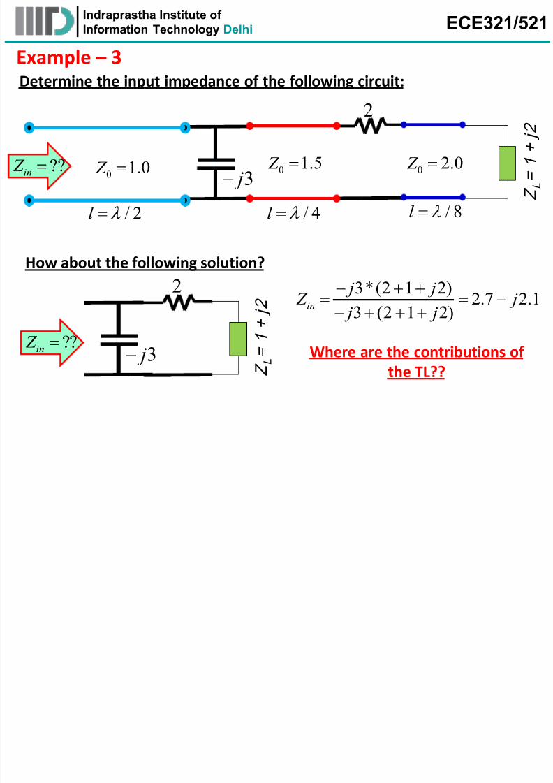
Example – 3Determine the input impedance of the following circuit:
Z
L =
1 + j 2
??in Z
2
3 j 0 2.0 Z 0 1.5 Z
0 1.0 Z
/ 8l / 4l / 2l
Z L =
1 + j 2
??in Z
2
3 j
How about the following solution?
3* (2 1 2) 2.7 2.13 (2 1 2)
in j j Z j j j
Where are the contributions of
the TL??
Indraprastha Institute ofECE321/521
7/21/2019 RF Circuit Design (ECE321/521)-Lect_4_2014
http://slidepdf.com/reader/full/rf-circuit-design-ece321521-lect42014 36/40
Indraprastha Institute of
Information Technology Delhi ECE321/521
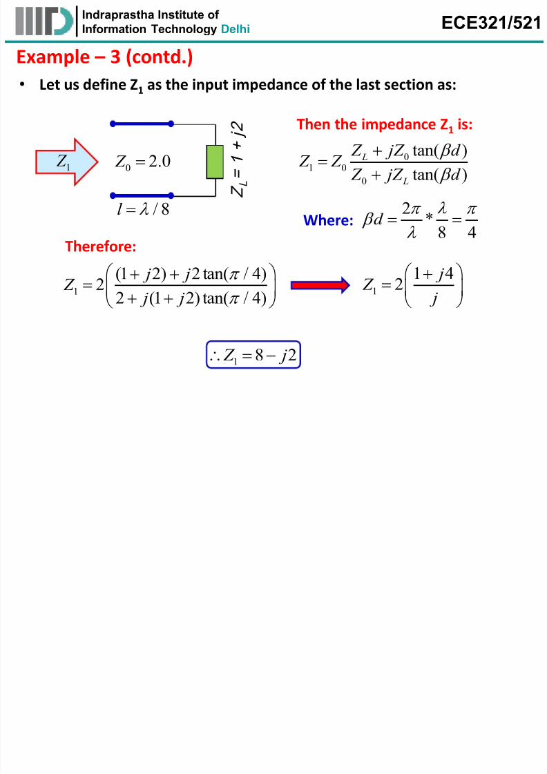
Example – 3 (contd.)
• Let us define Z1 as the input impedance of the last section as:
Z
L =
1 + j 2
1 Z 0 2.0 Z
/ 8l
01 0
0
tan( )
tan( )
L
L
Z jZ d Z Z
Z jZ d
Then the impedance Z1 is:
Where:2
*8 4
d
1
(1 2) 2 tan( / 4)
2 2 (1 2) tan( / 4)
j j
Z j j
Therefore:
1
1 4
2
j
Z j
1 8 2 Z j
Indraprastha Institute ofECE321/521
7/21/2019 RF Circuit Design (ECE321/521)-Lect_4_2014
http://slidepdf.com/reader/full/rf-circuit-design-ece321521-lect42014 37/40
Indraprastha Institute of
Information Technology Delhi ECE321/521
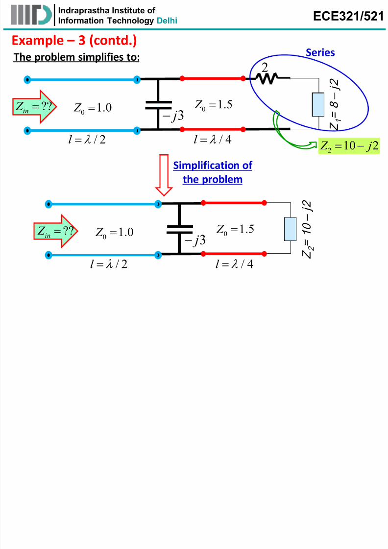
Example – 3 (contd.)
Z 1 =
8 –
j 2
??in
Z 3 j
0 1.5 Z 0 1.0 Z
/ 4l / 2l
2
The problem simplifies to: Series
Simplification of
the problem
Z 2 =
1 0
– j 2
??in Z
3 j 0 1.5 Z
0 1.0 Z
/ 4l / 2l
2 10 2 Z j
Indraprastha Institute ofECE321/521
7/21/2019 RF Circuit Design (ECE321/521)-Lect_4_2014
http://slidepdf.com/reader/full/rf-circuit-design-ece321521-lect42014 38/40
Indraprastha Institute of
Information Technology Delhi ECE321/521
Example – 3 (contd.)
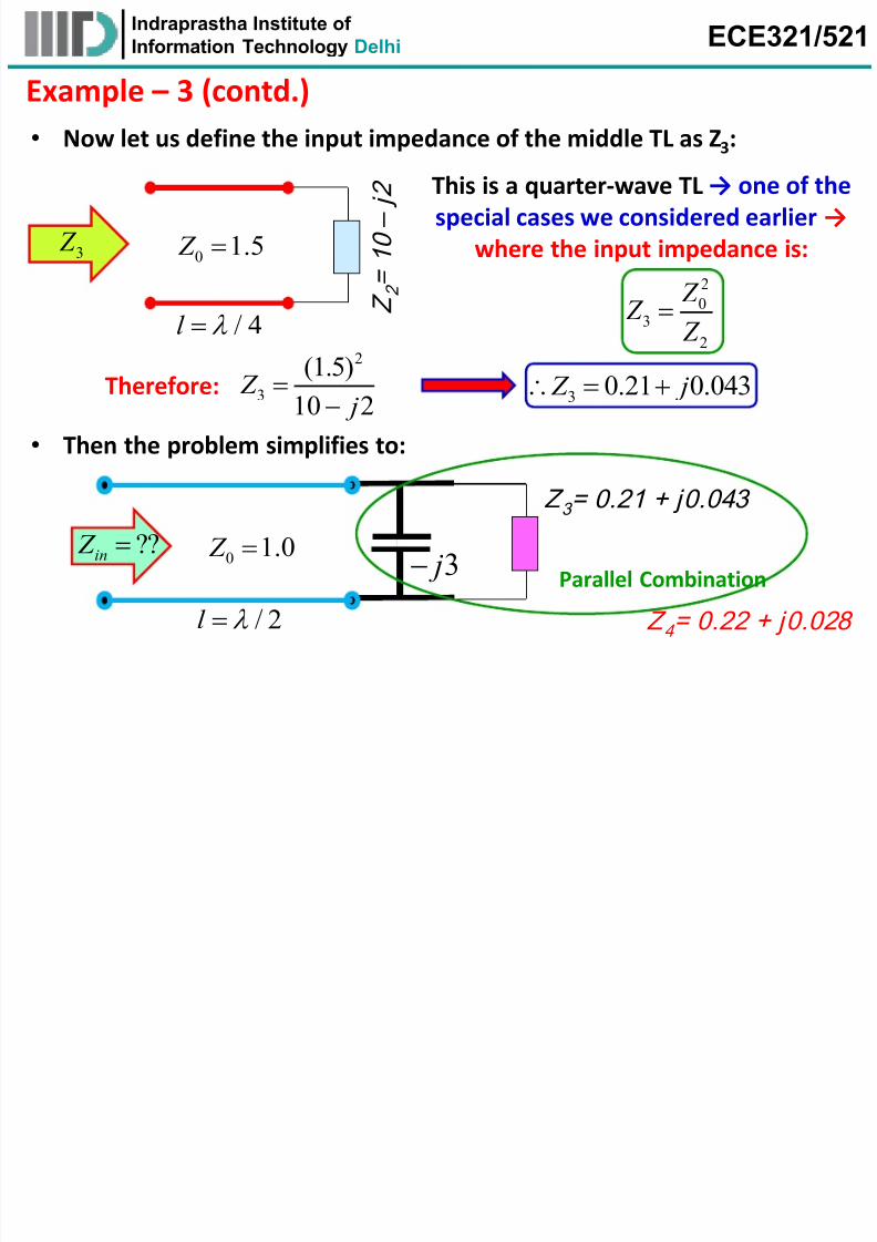
• Now let us define the input impedance of the middle TL as Z3:
2
3
(1.5)
10 2 Z
j
Therefore:
3 0.21 0.043 Z j
Z
2 =
1 0
–
j 2
3 Z 0 1.5 Z
/ 4l
This is a quarter-wave TL → one of the
special cases we considered earlier →
where the input impedance is:
2
03
2
Z Z Z
• Then the problem simplifies to:
Z 3 = 0.21 + j0.043
??in Z 3 j0 1.0 Z
/ 2l
Parallel Combination
Z 4 = 0.22 + j0.028
Indraprastha Institute ofECE321/521
7/21/2019 RF Circuit Design (ECE321/521)-Lect_4_2014
http://slidepdf.com/reader/full/rf-circuit-design-ece321521-lect42014 39/40
Indraprastha Institute of
Information Technology Delhi ECE321/521
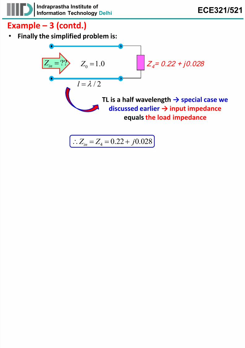
Example – 3 (contd.)• Finally the simplified problem is:
??in
Z 0 1.0 Z
/ 2l
Z 4 = 0.22 + j0.028
TL is a half wavelength → special case we
discussed earlier → input impedance
equals the load impedance
4 0.22 0.028in Z Z j
Indraprastha Institute ofECE321/521
7/21/2019 RF Circuit Design (ECE321/521)-Lect_4_2014
http://slidepdf.com/reader/full/rf-circuit-design-ece321521-lect42014 40/40
d ap ast a st tute o
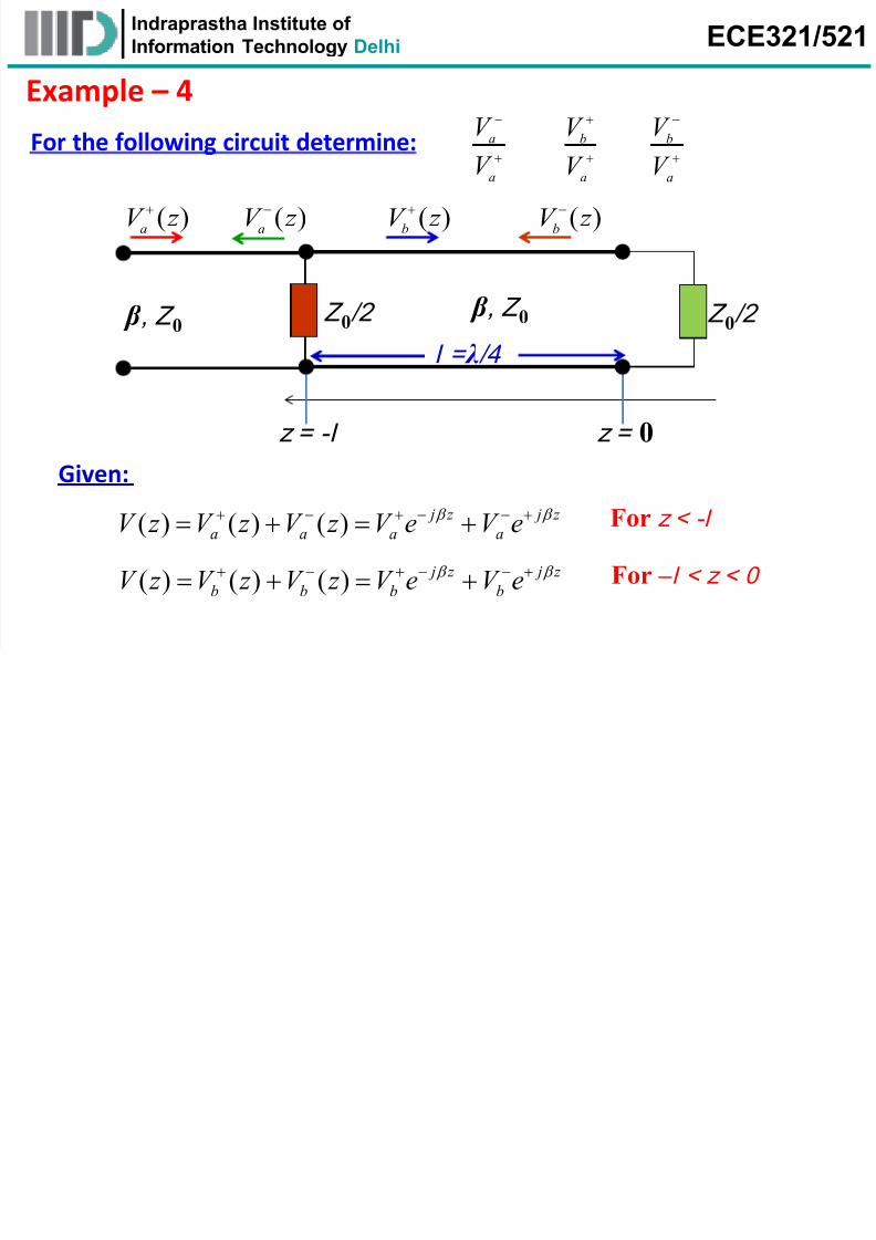
Information Technology Delhi ECE321/521
z = 0z = -l
β , Z 0 β , Z 0 Z 0 /2 Z 0 /2
l = λ /4
( )a
V z ( )
aV z
( )b
V z ( )
bV z
For the following circuit determine: a
a
V
V
b
a
V
V
b
a
V
V
Given:
( ) ( ) ( ) j z j z
a a a aV z V z V z V e V e For z < -l
( ) ( ) ( ) j z j z
b b b bV z V z V z V e V e For – l < z < 0
Example – 4