Embed Size (px)
Citation preview
RF DEVICE TESTING FOR MOBILE DEVICES
Korea Test Conference workshop 2015
Dusik YooSenior RF Applications Engineer
• Wireless Industry Trends
• RF Transceiver block diagram
• RF Transceiver Test Items
Contents
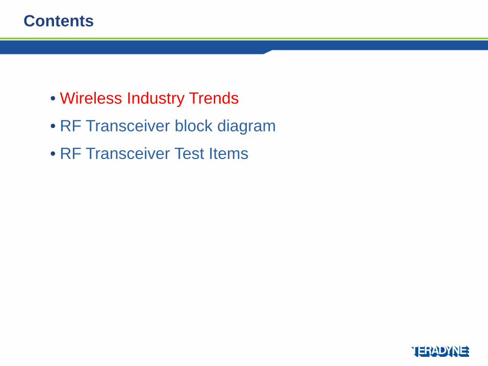
Smartphone & Tablet Continuing to Grow Worldwide• Units increasing by 340M units to 2.45B annually by 2018• Companies releasing 2x - 3x more new designs annually to meet
both premium & basic smart phone demands• Handset ASP shrinking by >5% YoY
Wireless Industry Trends
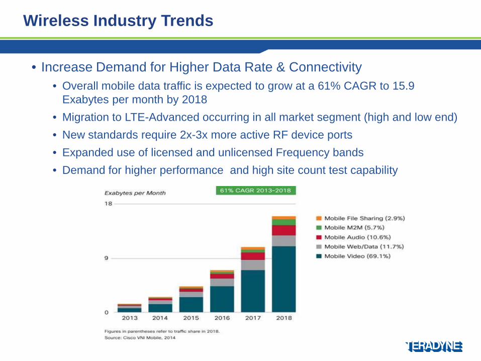
• Increase Demand for Higher Data Rate & Connectivity• Overall mobile data traffic is expected to grow at a 61% CAGR to 15.9
Exabytes per month by 2018• Migration to LTE-Advanced occurring in all market segment (high and low end)• New standards require 2x-3x more active RF device ports• Expanded use of licensed and unlicensed Frequency bands• Demand for higher performance and high site count test capability
Wireless Industry Trends
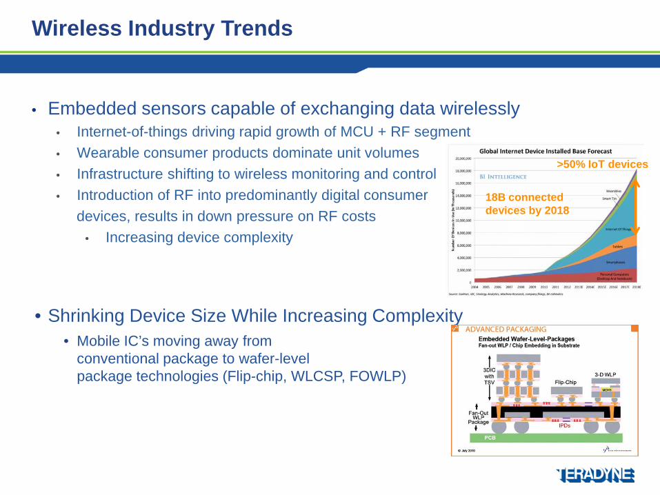
• Embedded sensors capable of exchanging data wirelessly• Internet-of-things driving rapid growth of MCU + RF segment• Wearable consumer products dominate unit volumes• Infrastructure shifting to wireless monitoring and control• Introduction of RF into predominantly digital consumer
devices, results in down pressure on RF costs• Increasing device complexity
• Shrinking Device Size While Increasing Complexity• Mobile IC’s moving away from
conventional package to wafer-level package technologies (Flip-chip, WLCSP, FOWLP)
Wireless Industry Trends
18B connected devices by 2018
>50% IoT devices
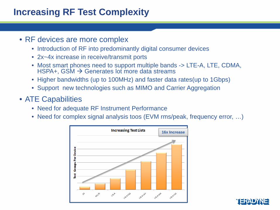
• RF devices are more complex • Introduction of RF into predominantly digital consumer devices• 2x~4x increase in receive/transmit ports• Most smart phones need to support multiple bands -> LTE-A, LTE, CDMA,
HSPA+, GSM Generates lot more data streams • Higher bandwidths (up to 100MHz) and faster data rates(up to 1Gbps)• Support new technologies such as MIMO and Carrier Aggregation
• ATE Capabilities• Need for adequate RF Instrument Performance • Need for complex signal analysis toos (EVM rms/peak, frequency error, …)
Increasing RF Test Complexity
16x Increase
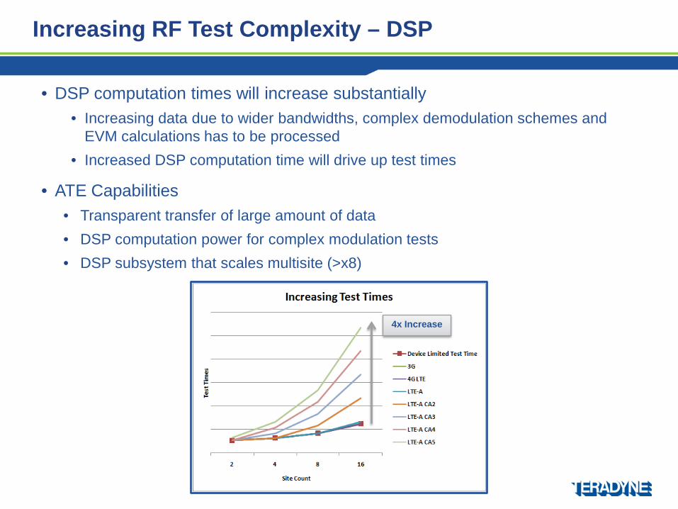
• DSP computation times will increase substantially • Increasing data due to wider bandwidths, complex demodulation schemes and
EVM calculations has to be processed• Increased DSP computation time will drive up test times
• ATE Capabilities• Transparent transfer of large amount of data• DSP computation power for complex modulation tests• DSP subsystem that scales multisite (>x8)
Increasing RF Test Complexity – DSP
4x Increase
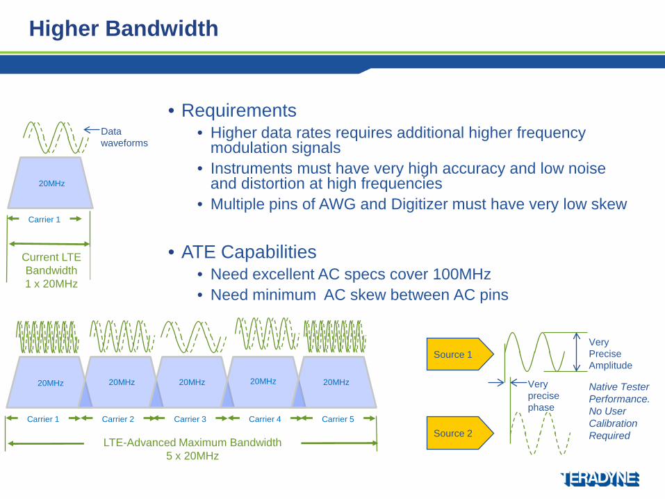
Higher Bandwidth
• Requirements• Higher data rates requires additional higher frequency
modulation signals• Instruments must have very high accuracy and low noise
and distortion at high frequencies• Multiple pins of AWG and Digitizer must have very low skew
• ATE Capabilities• Need excellent AC specs cover 100MHz• Need minimum AC skew between AC pins
LTE-Advanced Maximum Bandwidth5 x 20MHz
Carrier 1 Carrier 2 Carrier 3 Carrier 4 Carrier 5
20MHz 20MHz 20MHz 20MHz 20MHz
Current LTE Bandwidth1 x 20MHz
Carrier 1
20MHz
Source 1
Source 2
Very precise phase
Very Precise Amplitude
Data waveforms
Native Tester Performance. No User Calibration Required
0
1
2
3
4
5
6
7
0 25 50 75 100
125
150
175
200
225
250
275
300
325
350
375
400
425
450
475
500
% E
VM
I and Q Timing Skew effects on EVM
802.11ac 160M 256QAMLTE-Adv 100M 64 QAM802.11ac 80M 256QAM802.11ac 80M QPSK802.11ac 40M 256QAMLTE 20M 64QAM
802.11ac 160MEVM Limit = 2.51%
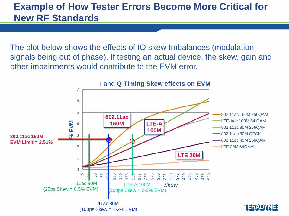
Example of How Tester Errors Become More Critical for New RF Standards
The plot below shows the effects of IQ skew Imbalances (modulation signals being out of phase). If testing an actual device, the skew, gain and other impairments would contribute to the EVM error.
LTE 20M
LTE-A 100M
Skew
11ac 80M (100ps Skew = 1-2% EVM)
802.11ac 160M
11ac 80M (25ps Skew = 0.5% EVM)
LTE-A 100M (200ps Skew = 2-3% EVM)
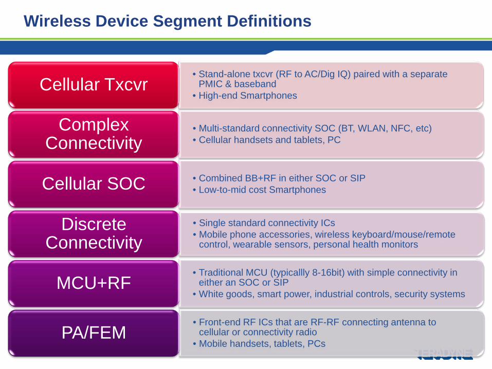
• Stand-alone txcvr (RF to AC/Dig IQ) paired with a separate PMIC & baseband
• High-end SmartphonesCellular Txcvr
• Multi-standard connectivity SOC (BT, WLAN, NFC, etc)• Cellular handsets and tablets, PC
Complex Connectivity
• Combined BB+RF in either SOC or SIP• Low-to-mid cost SmartphonesCellular SOC
• Single standard connectivity ICs• Mobile phone accessories, wireless keyboard/mouse/remote
control, wearable sensors, personal health monitors
Discrete Connectivity
• Traditional MCU (typicallly 8-16bit) with simple connectivity in either an SOC or SIP
• White goods, smart power, industrial controls, security systemsMCU+RF
• Front-end RF ICs that are RF-RF connecting antenna to cellular or connectivity radio
• Mobile handsets, tablets, PCsPA/FEM
Wireless Device Segment Definitions
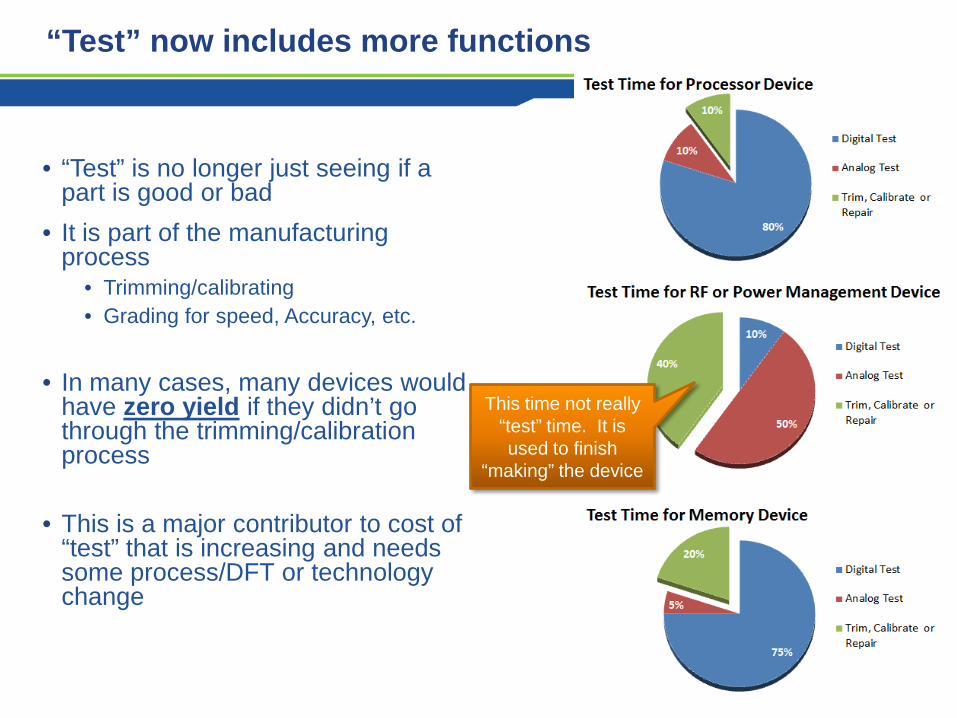
• “Test” is no longer just seeing if a part is good or bad
• It is part of the manufacturing process
• Trimming/calibrating• Grading for speed, Accuracy, etc.
• In many cases, many devices would have zero yield if they didn’t go through the trimming/calibration process
• This is a major contributor to cost of “test” that is increasing and needs some process/DFT or technology change
“Test” now includes more functions
This time not really “test” time. It is used to finish
“making” the device
• Wireless Industry Trends
• Transceiver block diagram
• RF Transceiver Test Items
Contents
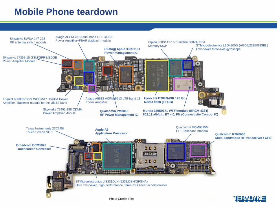
Mobile Phone teardown
Skyworks 77352-15 GSM/GPRS/EDGE Power Amplifier Module
Skyworks SWUA 147 228 RF antenna switch module
Triquint 666083-1229 WCDMA / HSUPA Power Amplifier / duplexer module for the UMTS band
Avago AFEM-7813 dual-band LTE B1/B3 Power Amplifier+FBAR duplexer module
Skyworks 77491-158 CDMAPower Amplifier Module
Avago A5613 ACPM-5613 LTE band 13 Power Amplifier
Qualcomm PM8018 RF Power Management IC
Hynix H2JTDG2MBR 128 GbNAND flash (16 GB)
Murata 339S0171 Wi-Fi module (BRCM 4334) 802.11 a/b/g/n, BT 4.0, FM (Connectivity Combo IC)
(Dialog) Apple 338S1131Power management IC
Elpida 338S1117 or SanDisk SDMALBB4 Memory MCP STMicroelectronics L3G4200D (AGD5/2235/G8SBI )
Low-power three-axis gyroscope
Apple A6Application Processor
STMicroelectronics LIS331DLH (2233/DSH/GFGHA) Ultra low-power, high performance, three-axis linear accelerometer
Texas Instruments 27C245I Touch Screen SOC
Broadcom BCM5976 Touchscreen Controller
Qualcomm MDM9615M LTE Baseband modem
Qualcomm RTR8600 Multi-band/mode RF transceiver / GPS
Photo Credit: iFixit
Mobile Phone Front End Block
Photo Credit: Techinsights
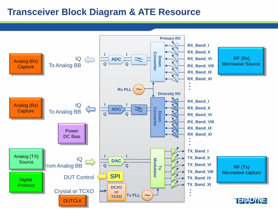
Crystal or TCXO
Rx PLL ~
I
QADC
I
QD
own
Converter
RX_Band_IRX_Band_IIRX_Band_VIRX_Band_VIII
Primary RX
Diversity RX
Dow
nC
onverter
TX_Band_VIII
I
Q
I
Q
I
QDAC
I
Q
TX_Band_ITX_Band_IITX_Band_VI
Tx PLL ~
SPIDCXO
orTCXO
RX_Band_IRX_Band_IIRX_Band_VIRX_Band_VIII
……
…
ADC
IQTo Analog BB
IQTo Analog BB
IQFrom Analog BB
DUT Control
RX_Band_IXRX_Band_XI
RX_Band_IXRX_Band_XI
TX_Band_XITX_Band_IX
TxM
odulator
Page 15
RF (Rx)Microwave Source
RF (Tx)Microwave capture
Analog (Rx)Capture
Analog (TX)Source
Analog (Rx)Capture
PowerDC Bias
Digital Protocol
Transceiver Block Diagram & ATE Resource
DUTCLK
Contents
• Wireless Industry Trends
• Transceiver block diagram
• RF Transceiver Test Items
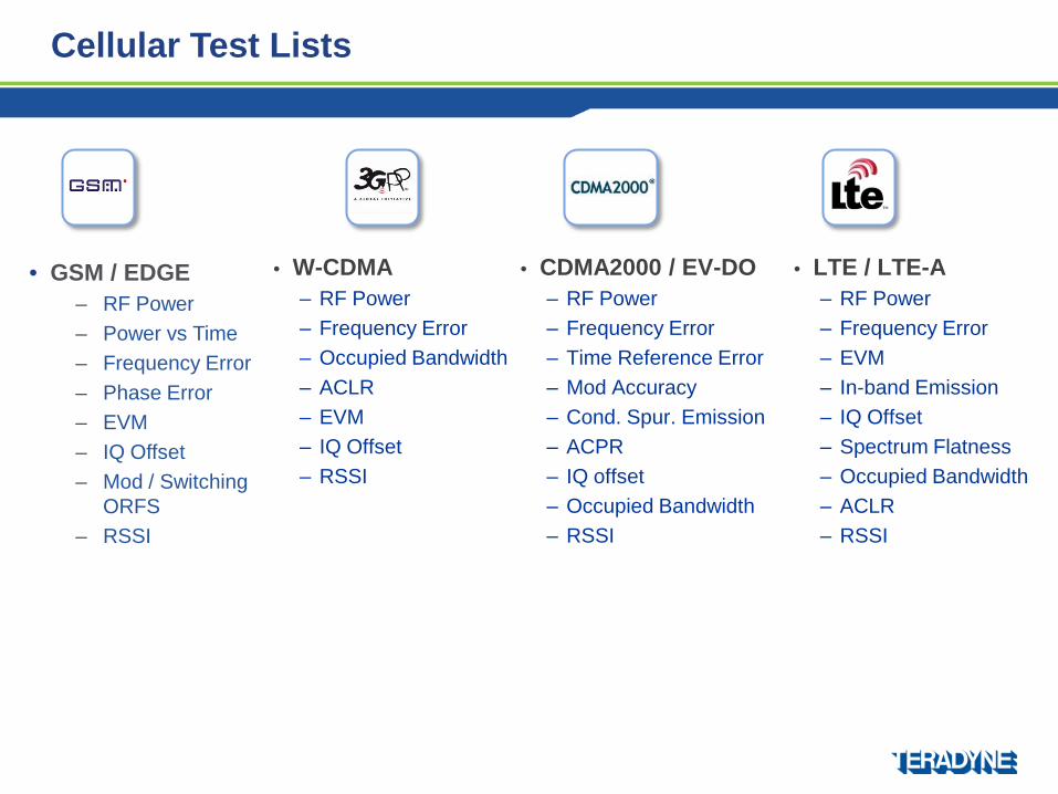
Cellular Test Lists
• GSM / EDGE– RF Power– Power vs Time– Frequency Error– Phase Error– EVM– IQ Offset– Mod / Switching
ORFS– RSSI
• W-CDMA‒ RF Power‒ Frequency Error‒ Occupied Bandwidth‒ ACLR‒ EVM‒ IQ Offset‒ RSSI
• LTE / LTE-A‒ RF Power‒ Frequency Error‒ EVM‒ In-band Emission‒ IQ Offset‒ Spectrum Flatness‒ Occupied Bandwidth‒ ACLR‒ RSSI
• CDMA2000 / EV-DO‒ RF Power‒ Frequency Error‒ Time Reference Error‒ Mod Accuracy‒ Cond. Spur. Emission‒ ACPR‒ IQ offset‒ Occupied Bandwidth‒ RSSI
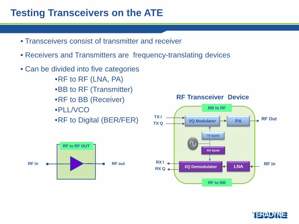
• Transceivers consist of transmitter and receiver
• Receivers and Transmitters are frequency-translating devices
• Can be divided into five categories•RF to RF (LNA, PA)•BB to RF (Transmitter)•RF to BB (Receiver)•PLL/VCO•RF to Digital (BER/FER)
RF in RF out
RF to RF DUT
RF Transceiver Device
TX ITX Q PA
RX IRX Q I/Q Demodulator LNA
RF Out
RF In
TX Synth
RX Synth
I/Q Modulator
BB to RF
RF to BB
Testing Transceivers on the ATE
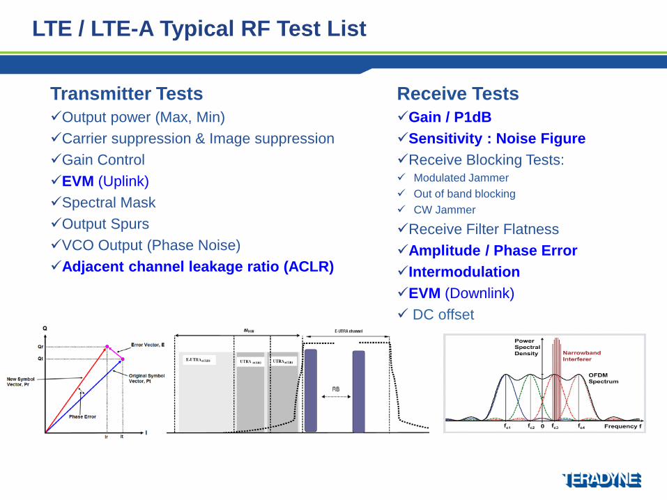
LTE / LTE-A Typical RF Test List
Transmitter TestsOutput power (Max, Min)Carrier suppression & Image suppressionGain ControlEVM (Uplink)Spectral MaskOutput SpursVCO Output (Phase Noise)Adjacent channel leakage ratio (ACLR)
Receive TestsGain / P1dBSensitivity : Noise FigureReceive Blocking Tests: Modulated Jammer Out of band blocking CW Jammer
Receive Filter FlatnessAmplitude / Phase ErrorIntermodulationEVM (Downlink) DC offset
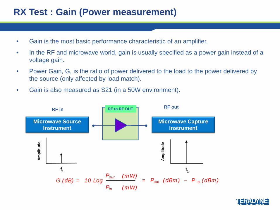
RX Test : Gain (Power measurement)
• Gain is the most basic performance characteristic of an amplifier.
• In the RF and microwave world, gain is usually specified as a power gain instead of a voltage gain.
• Power Gain, G, is the ratio of power delivered to the load to the power delivered by the source (only affected by load match).
• Gain is also measured as S21 (in a 50W environment).
G (dB) = 10 LogPout (mW)
Pin (mW)= Pout (dBm) – P in (dBm)
RF in RF outRF to RF DUT
Microwave Source Instrument
Microwave Capture Instrument
f1
Ampl
itude
f1
Ampl
itude
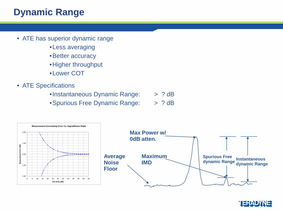
Dynamic Range
• ATE has superior dynamic range•Less averaging•Better accuracy•Higher throughput•Lower COT
• ATE Specifications•Instantaneous Dynamic Range: > ? dB•Spurious Free Dynamic Range: > ? dB
Spurious Free dynamic Range
Maximum IMD
Average Noise Floor
Instantaneous dynamic Range
Max Power w/ 0dB atten.
Measurement Uncertainty Error Vs. Signal/Noise Ratio
-2.00
-1.00
0.00
1.00
2.00
0 5 10 15 20 25 30 35 40 45 50 55 60
S/N delta (dB)
Mea
sure
men
t Err
or (d
B)
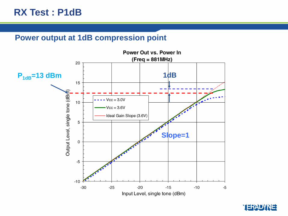
RX Test : P1dB
Power output at 1dB compression point
P1dB=13 dBm 1dB
Slope=1
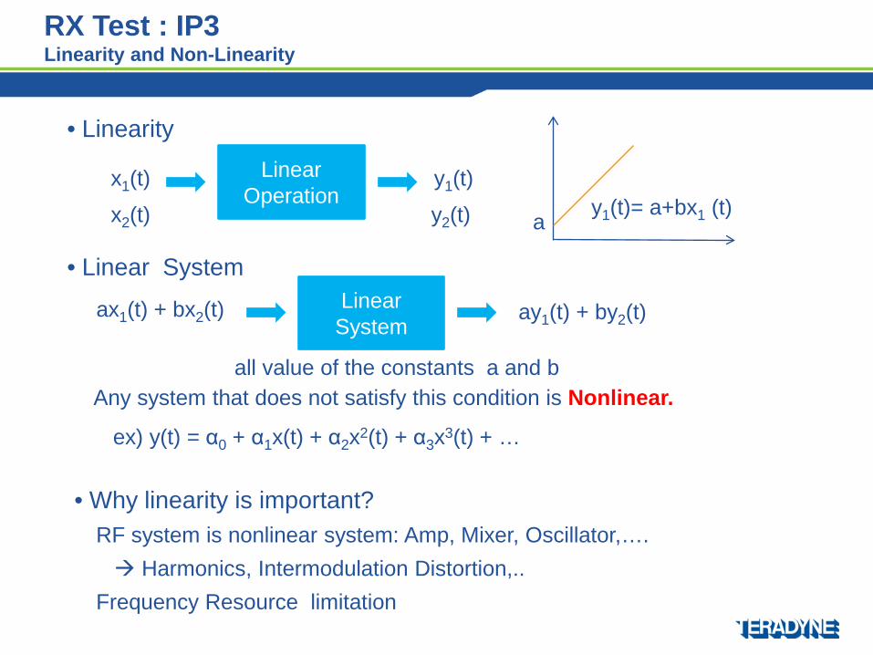
RX Test : IP3Linearity and Non-Linearity
Linear Operation
x1(t) y1(t) y1(t)= a+bx1 (t)x2(t) y2(t) a
Linear System
ax1(t) + bx2(t) ay1(t) + by2(t)
all value of the constants a and bAny system that does not satisfy this condition is Nonlinear.
ex) y(t) = α0 + α1x(t) + α2x2(t) + α3x3(t) + …
• Linearity
• Linear System
• Why linearity is important?RF system is nonlinear system: Amp, Mixer, Oscillator,…. Harmonics, Intermodulation Distortion,..
Frequency Resource limitation
DC Fundamental Harmonics
Frequency
f
2f3f 4f 5f
Fundamental frequency
Am
plitu
de
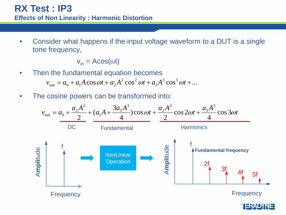
• Consider what happens if the input voltage waveform to a DUT is a single tone frequency,
vin = Acos(ωt)• Then the fundamental equation becomes
• The cosine powers can be transformed into:
...coscoscos 333
22210 ++++= tAatAatAaavout ωωω
tAatAatAaAaAaavout ωωω 3cos4
2cos2
cos)4
3(2
33
22
33
1
22
0 +++++=
NonLinearOperation
Frequency
f
Am
plitu
de
RX Test : IP3Effects of Non Linearity : Harmonic Distortion
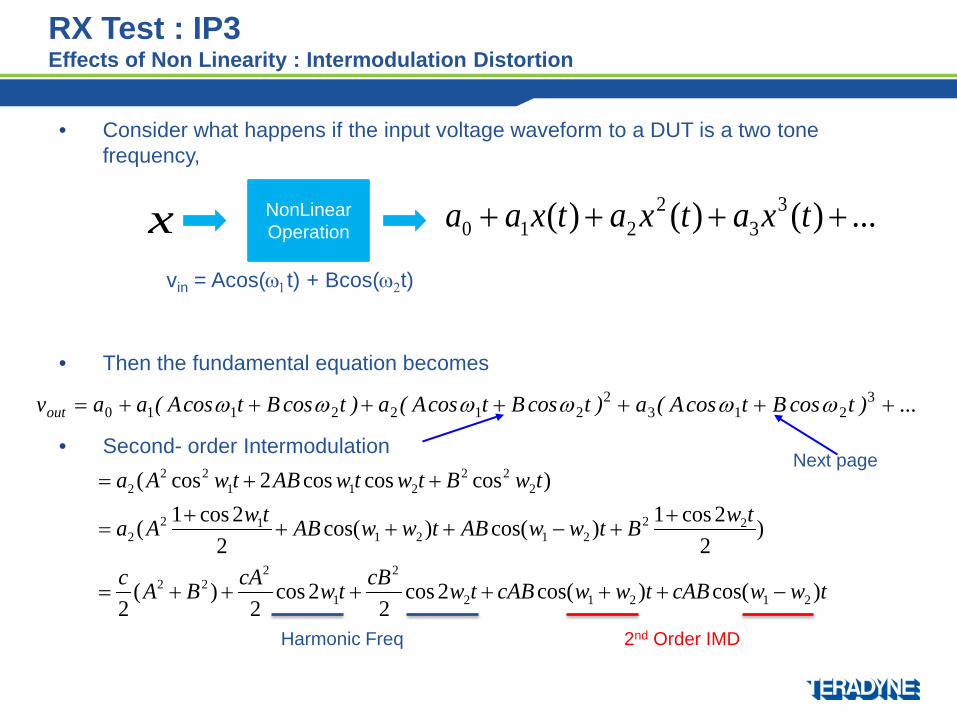
• Consider what happens if the input voltage waveform to a DUT is a two tone frequency,
vin = Acos(ω1t) + Bcos(ω2t)
• Then the fundamental equation becomes
• Second- order Intermodulation
22122110 )tcosBtcosA(a)tcosBtcosA(aavout ωωωω ++++= ...)tcosBtcosA(a +++ 3
213 ωω
x
twwcABtwwcABtwcBtwcABAc
twBtwwABtwwABtwAa
twBtwtwABtwAa
)cos()cos(2cos2
2cos2
)(2
)2
2cos1)cos()cos(2
2cos1(
)coscoscos2cos(
21212
2
1
222
222121
122
222
21122
2
−++++++=
++−+++
+=
++=Next page
Harmonic Freq 2nd Order IMD
NonLinearOperation ...)()()( 3
32
210 ++++ txatxatxaa
RX Test : IP3Effects of Non Linearity : Intermodulation Distortion
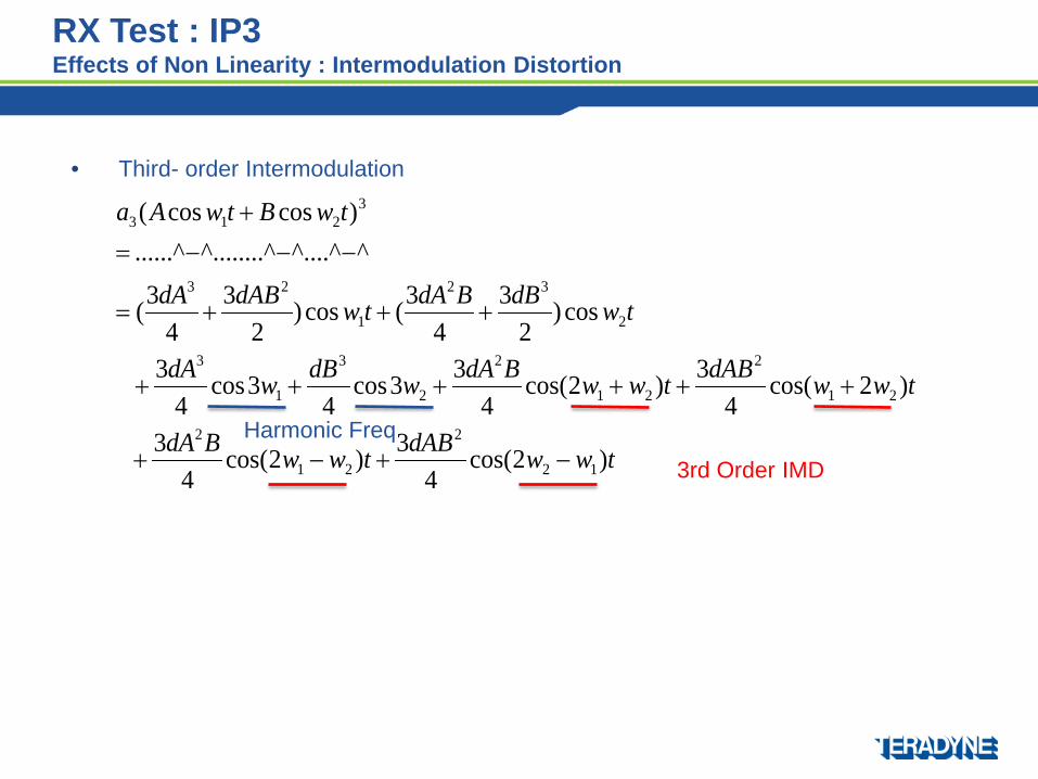
• Third- order Intermodulation
twwdABtwwBdA
twwdABtwwBdAwdBwdA
twdBBdAtwdABdA
twBtwAa
)2cos(4
3)2cos(4
3
)2cos(4
3)2cos(4
33cos4
3cos4
3
cos)2
34
3(cos)2
34
3(
^^....^^........^......^)coscos(
12
2
21
2
21
2
21
2
2
3
1
3
2
32
1
23
3213
−+−+
++++++
+++=
−−−=+
Harmonic Freq
3rd Order IMD
RX Test : IP3Effects of Non Linearity : Intermodulation Distortion
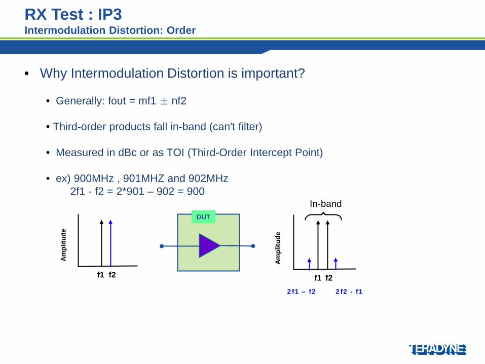
• Why Intermodulation Distortion is important?
• Generally: fout = mf1 ± nf2
• Third-order products fall in-band (can't filter)
• Measured in dBc or as TOI (Third-Order Intercept Point)
• ex) 900MHz , 901MHZ and 902MHz2f1 - f2 = 2*901 – 902 = 900
In-bandDUT
f1
Ampl
itude
f2 f1Am
plitu
def2
2f2 - f12f1 – f2
RX Test : IP3Intermodulation Distortion: Order
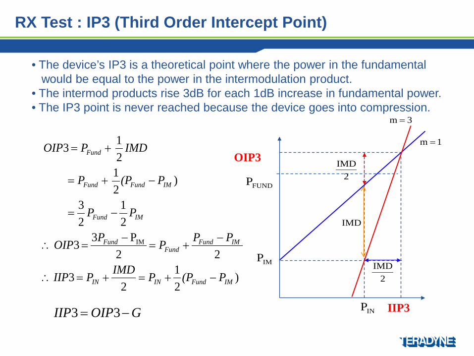
RX Test : IP3 (Third Order Intercept Point)
)21
23
22P33
21
23
)21213
IM
IMFundININ
IMFundFund
Fund
IMFund
IMFundFund
Fund
P(PPIMDPIIP
PPPPOIP
PP
P(PP
IMDPOIP
−+=+=∴
−+=
−=∴
−=
−+=
+=OIP3
IIP3INP
IMP
FUNDP 2IMD
2IMD
IMD
1m =
3m =
• The device’s IP3 is a theoretical point where the power in the fundamental would be equal to the power in the intermodulation product.
• The intermod products rise 3dB for each 1dB increase in fundamental power.• The IP3 point is never reached because the device goes into compression.
GOIPIIP −= 33
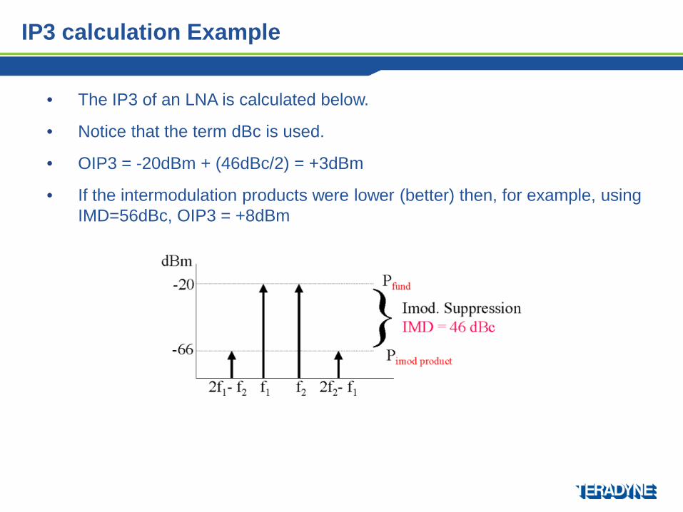
• The IP3 of an LNA is calculated below.
• Notice that the term dBc is used.
• OIP3 = -20dBm + (46dBc/2) = +3dBm
• If the intermodulation products were lower (better) then, for example, using IMD=56dBc, OIP3 = +8dBm
IP3 calculation Example
RX Test : IP3
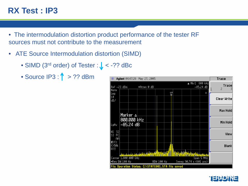
• The intermodulation distortion product performance of the tester RF sources must not contribute to the measurement
• ATE Source Intermodulation distortion (SIMD)
• SIMD (3rd order) of Tester : < -?? dBc
• Source IP3 : > ?? dBm
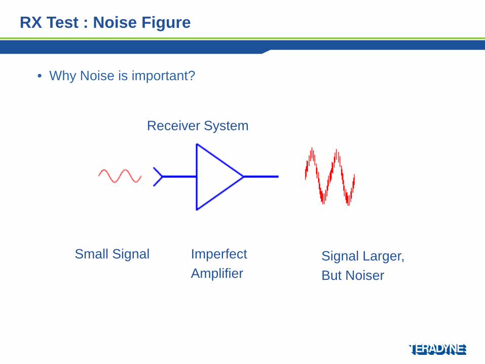
Receiver System
Small Signal Imperfect Amplifier
Signal Larger,But Noiser
RX Test : Noise Figure
• Why Noise is important?
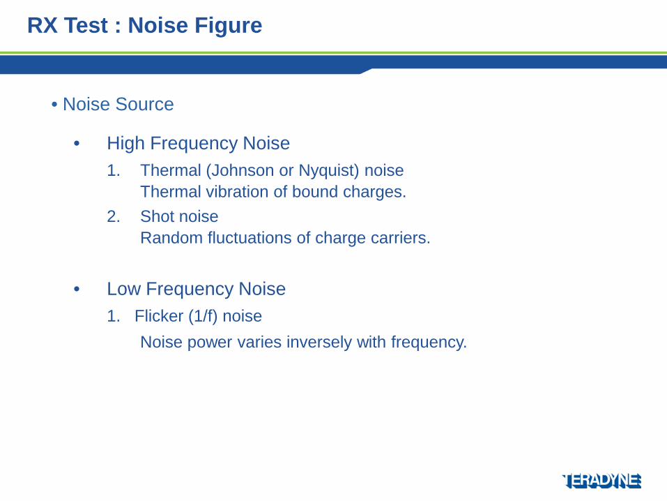
• High Frequency Noise1. Thermal (Johnson or Nyquist) noise
Thermal vibration of bound charges.2. Shot noise
Random fluctuations of charge carriers.
• Low Frequency Noise1. Flicker (1/f) noise
Noise power varies inversely with frequency.
RX Test : Noise Figure
• Noise Source
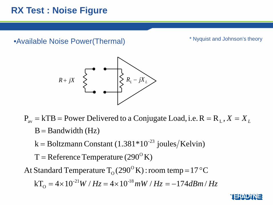
HzdBmHzmWHzW
XX L
/174/104/104kT
C 17 temproom :K)290(T eTemperatur StandardAt K)(290 eTemperatur Reference T
)Kelvinjoules10*(1.381Constant Boltzmann k (Hz)Bandwidth B
,RR i.e. Load, Conjugate a toDeliveredPower kTBP
18-21-O
OO
O
23-
Lav
−=×=×=
°=
=
=
=====
* Nyquist and Johnson’s theory•Available Noise Power(Thermal)
LL jXR −jXR +
RX Test : Noise Figure
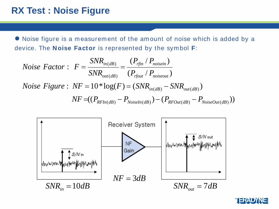
))()((
)()log(*10:
)/()/(
:
)()()()(
)()(
)(
)(
dBNoiseOutdBRFOutdBNoiseIndBRFIn
dBoutdBin
noiseoutrfout
noiseinrfin
dBout
dBin
PPPPNFSNRSNRFNFFigureNoise
PPPP
SNRSNR
FFactorNoise
−−−=
−==
==
Noise figure is a measurement of the amount of noise which is added by a device. The Noise Factor is represented by the symbol F:
dBSNRin 10=dBNF 3=
dBSNRout 7=
RX Test : Noise Figure
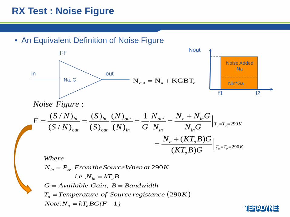
KTTo
oa
KTTin
ina
in
out
in
out
out
in
out
in
oa
oa
GBKTGBKTN
GNGNN
NN
GNN
SS
NSNSF
FigureNoise
290
290
)()(
1)()(
)()(
)/()/(
:
==
==
+=
+====
Na, Goutin
IRE
f1 f2
Nin*Ga
Noise Added Na
Nout
( ))BG(FkTNote:N
KregistanceSourceofeTemperaturTBandwidthBGain,AvailableG
BkTi.e.,NKatWhenSourcetheFromPN
Where
oa
o
oin
avin
1290
290
−==
===
=
• An Equivalent Definition of Noise Figure
oaout KGBTNN +=
RX Test : Noise Figure
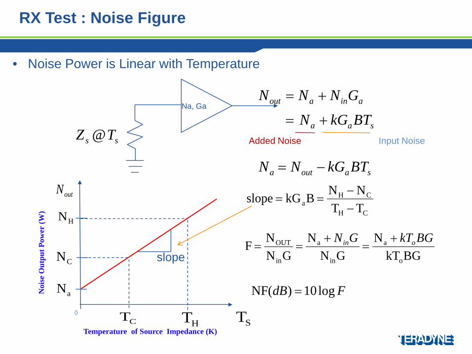
Na, Ga
outN
ss TZ @
saouta
saa
ainaout
BTkGNN
BTkGNGNNN
−=
+=
+=
CT0
HT
aN
CN
HN
Noi
se O
utpu
t Pow
er (W
)
Temperature of Source Impedance (K) ST
CH
CHa TT
NNBkGslope−−
==
BGkTN
GNN
GNNF
o
a
in
a
in
OUT BGkTGN oin +=
+==
FdB log10)(NF =
slope
• Noise Power is Linear with Temperature
Input NoiseAdded Noise
RX Test : Noise Figure

• The Y-Factor method of measuring NF uses a noise source applied to the input of the DUT to supply two different noise power levels to the DUT
• Power measurements over as specified bandwidth are made at the DUT for each of the two applied noise power levels
• The Y-factor is defined as:
• The Y-Factor can also be expressed in dB.Y|dB = Pmeasured,hot|dB – Pmeasured,cold|dB
coldmeasured
hotmeasured
PP
Y,
,=
TesterNoise SourceON
DUT
Noise SourceOFF (50 ohms)
TesterDUT
Step 1 (hot noise power measurement)
Step 2 (cold noise power measurement)
• Y-Factor Method of Measuring NF
RX Test : Noise Figure
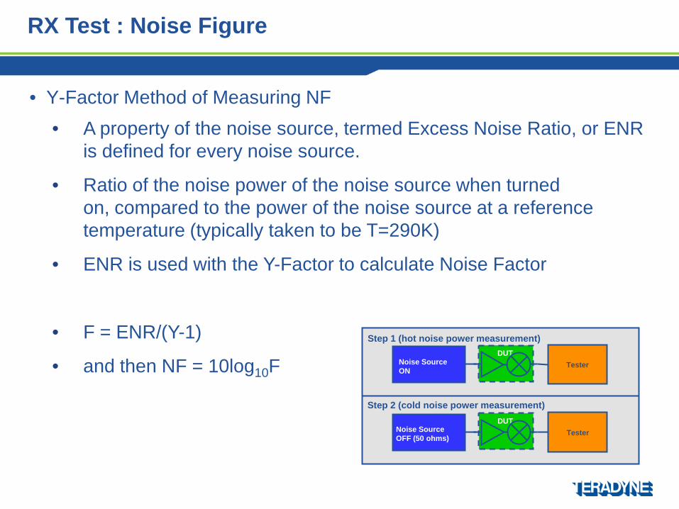
• A property of the noise source, termed Excess Noise Ratio, or ENR is defined for every noise source.
• Ratio of the noise power of the noise source when turned on, compared to the power of the noise source at a reference temperature (typically taken to be T=290K)
• ENR is used with the Y-Factor to calculate Noise Factor
• F = ENR/(Y-1)
• and then NF = 10log10F TesterNoise SourceON
DUT
Noise SourceOFF (50 ohms)
TesterDUT
Step 1 (hot noise power measurement)
Step 2 (cold noise power measurement)
• Y-Factor Method of Measuring NF
RX Test : Noise Figure
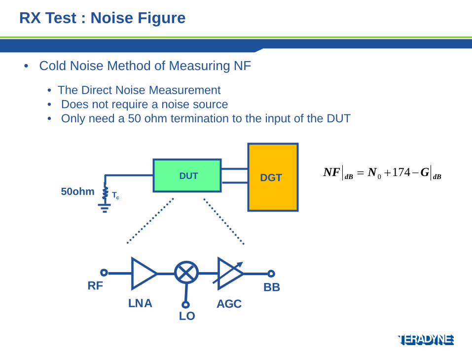
DUT
Tc
RF
LO
BBLNA AGC
DGT dBdB GNNF −+= 1740
• The Direct Noise Measurement• Does not require a noise source• Only need a 50 ohm termination to the input of the DUT
• Cold Noise Method of Measuring NF
50ohm
RX Test : Noise Figure
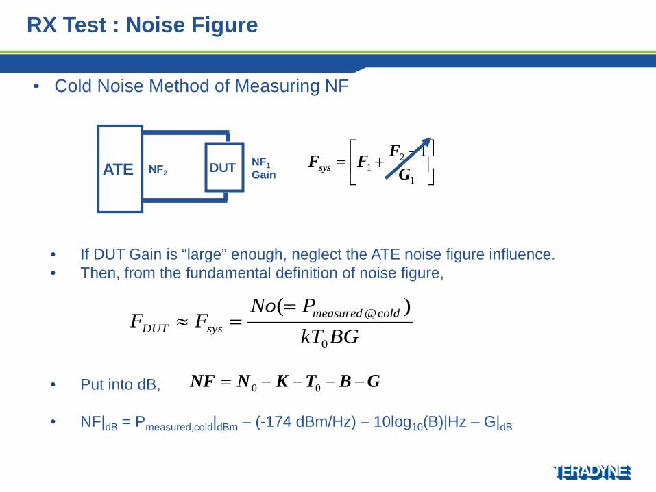
• If DUT Gain is “large” enough, neglect the ATE noise figure influence. • Then, from the fundamental definition of noise figure,
• Put into dB,
• NF|dB = Pmeasured,cold|dBm – (-174 dBm/Hz) – 10log10(B)|Hz – G|dB
−+=
1
21
1G
FFFsysATE DUT NF1GainNF2
BGkTPNo
FF coldmeasuredsysDUT
0
@ )(==≈
GBTKNNF −−−−= 00
• Cold Noise Method of Measuring NF
RX Test : Noise Figure
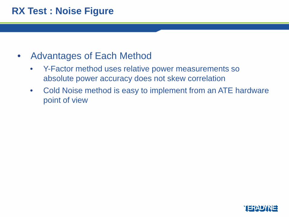
• Advantages of Each Method • Y-Factor method uses relative power measurements so
absolute power accuracy does not skew correlation• Cold Noise method is easy to implement from an ATE hardware
point of view
RX Test : Noise Figure
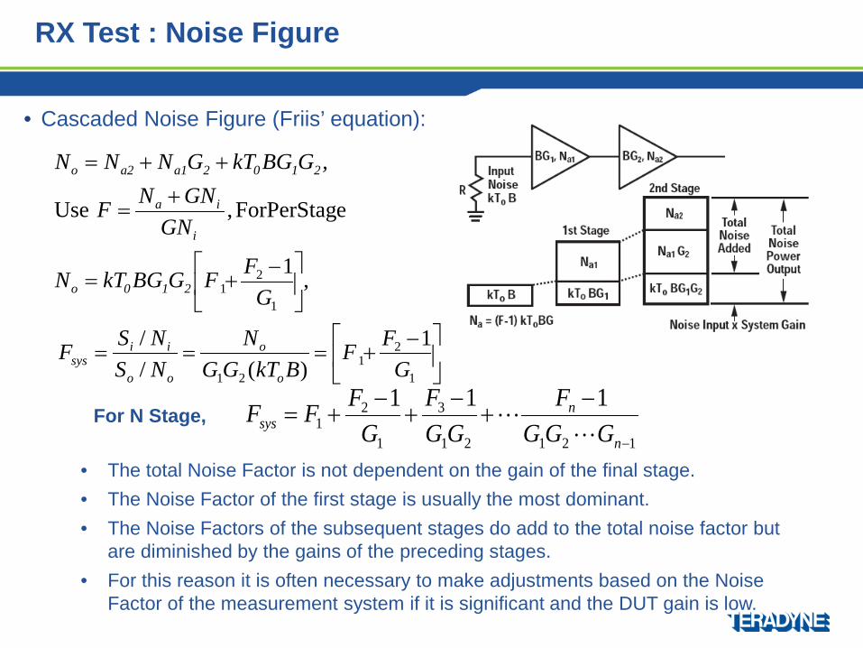
• Cascaded Noise Figure (Friis’ equation):
• The total Noise Factor is not dependent on the gain of the final stage.• The Noise Factor of the first stage is usually the most dominant. • The Noise Factors of the subsequent stages do add to the total noise factor but
are diminished by the gains of the preceding stages.• For this reason it is often necessary to make adjustments based on the Noise
Factor of the measurement system if it is significant and the DUT gain is low.
−+===
−+=
+=
++=
1
21
21
1
21
1)(/
/
,1
eForPerStag,Use
GFF
BkTGGN
NSNSF
GFFGBGkTN
GNGNNF
,GBGkTGNNN
o
o
oo
iisys
210o
i
ia
2102a1a2o
12121
3
1
21
111
−
−+
−+
−+=
n
nsys GGG
FGG
FG
FFF
For N Stage,
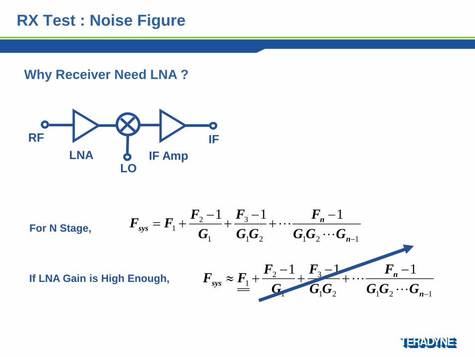
RX Test : Noise Figure
RF
LO
IFLNA
Why Receiver Need LNA ?
12121
3
1
21
111
−
−+
−+
−+=
n
nsys GGG
FGG
FG
FFF
For N Stage,
IF Amp
12121
3
1
21
111
−
−+
−+
−+≈
n
nsys GGG
FGG
FG
FFF
If LNA Gain is High Enough,
RX Test : Noise Figure
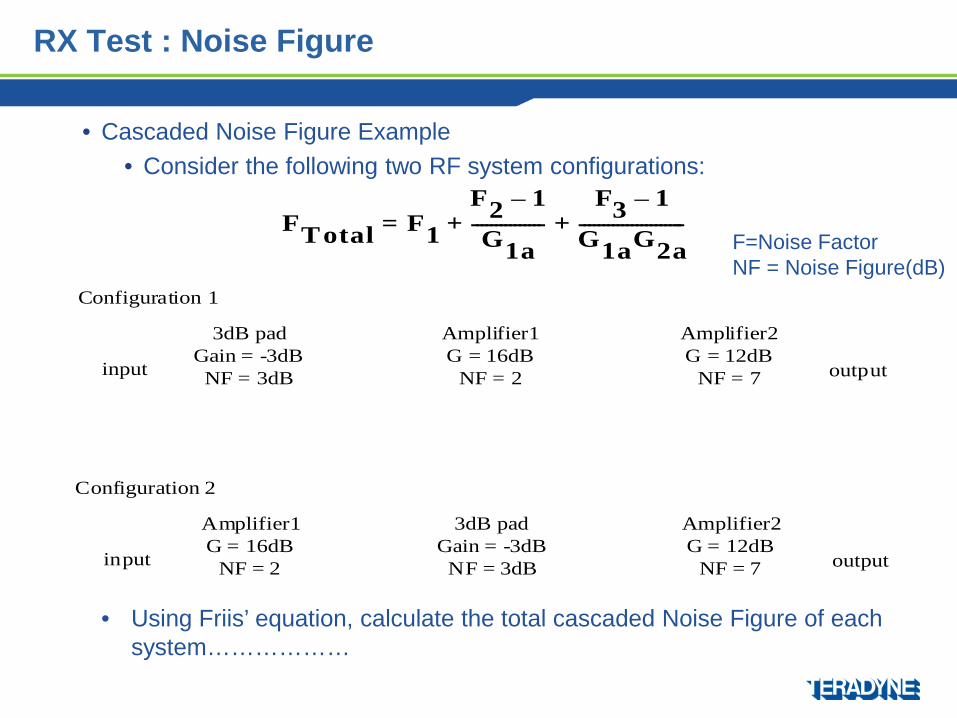
• Cascaded Noise Figure Example• Consider the following two RF system configurations:
• Using Friis’ equation, calculate the total cascaded Noise Figure of each system………………
input
FTotal F1=F2 1–
G1a---------------
F3 1–
G1aG2a----------------------+ +
output
Amplifier2G = 12dB
NF = 7
Amplifier1G = 16dB
NF = 2
3dB padGain = -3dB
NF = 3dB
input output
Amplifier2G = 12dB
NF = 7
3dB padGain = -3dB
NF = 3dB
Amplifier1G = 16dB
NF = 2
Configuration 1
Configuration 2
RX Test : Noise Figure
F=Noise FactorNF = Noise Figure(dB)
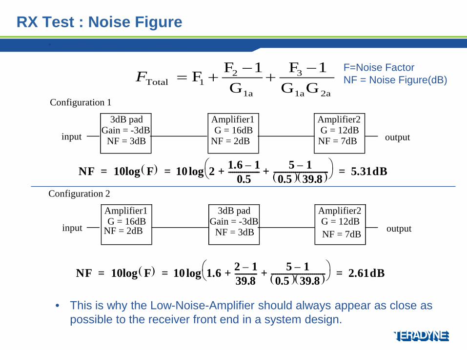
• Cascaded Noise Figure Example:
• This is why the Low-Noise-Amplifier should always appear as close as possible to the receiver front end in a system design.
NF 10 F( )log 10 2 1.6 1–0.5
---------------- 5 1–0.5( ) 39.8( )----------------------------+ +
log 5.31dB= = =
NF 10 F( )log 10 1.6 2 1–39.8------------ 5 1–
0.5( ) 39.8( )----------------------------+ + log 2.61dB= = =
input output
Amplifier2G = 12dB
NF = 7dB
Amplifier1G = 16dB
NF = 2dB
3dB padGain = -3dB
NF = 3dB
input output
Amplifier2G = 12dBNF = 7dB
3dB padGain = -3dB
NF = 3dB
Amplifier1G = 16dB
NF = 2dB
Configuration 1
Configuration 2
2a1a
3
1a
21 Total GG
1FG
1FF −+
−+=F
RX Test : Noise Figure
F=Noise FactorNF = Noise Figure(dB)
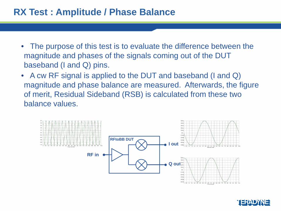
RX Test : Amplitude / Phase Balance
• The purpose of this test is to evaluate the difference between the magnitude and phases of the signals coming out of the DUT baseband (I and Q) pins.
• A cw RF signal is applied to the DUT and baseband (I and Q) magnitude and phase balance are measured. Afterwards, the figure of merit, Residual Sideband (RSB) is calculated from these two balance values.
I out
Q out
RF in
RFtoBB DUT
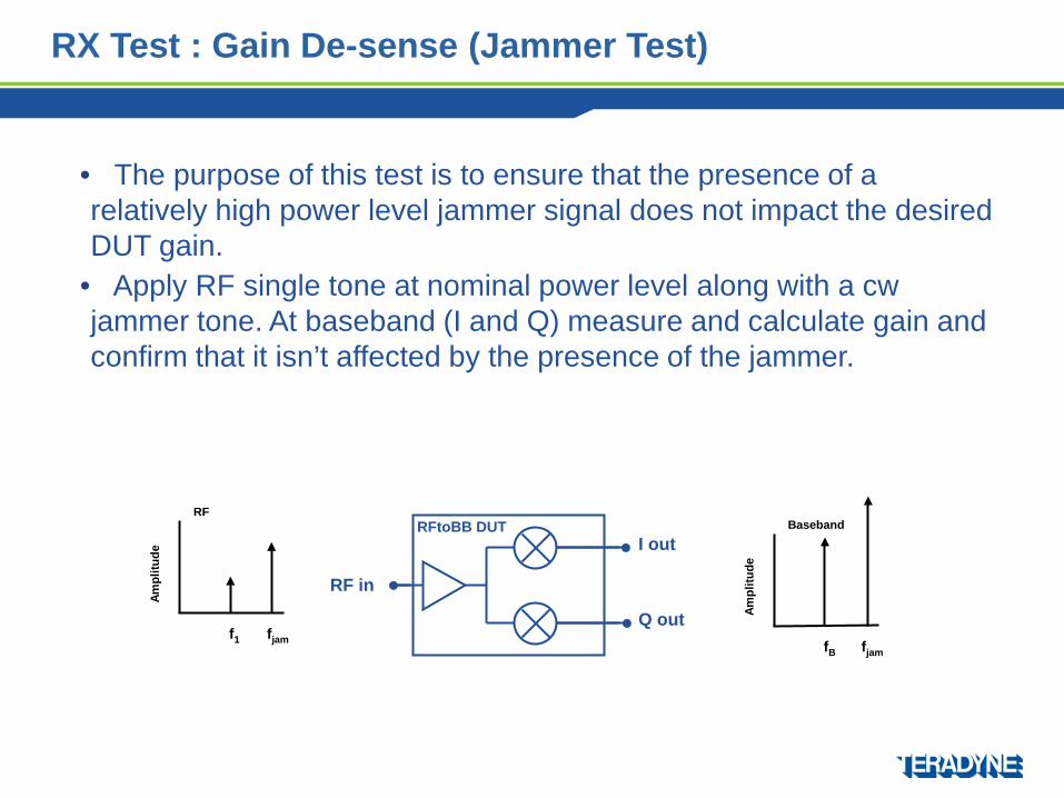
RX Test : Gain De-sense (Jammer Test)
• The purpose of this test is to ensure that the presence of a relatively high power level jammer signal does not impact the desired DUT gain.
• Apply RF single tone at nominal power level along with a cwjammer tone. At baseband (I and Q) measure and calculate gain and confirm that it isn’t affected by the presence of the jammer.
I out
Q out
RF in
RFtoBB DUT
f1
Ampl
itude
RF
fjam fB
Ampl
itude
Baseband
fjam
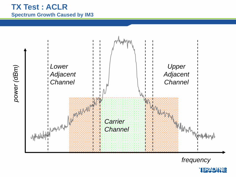
TX Test : ACLRSpectrum Growth Caused by IM3
frequency
Lower Adjacent Channel
Upper AdjacentChannel
Carrier Channel
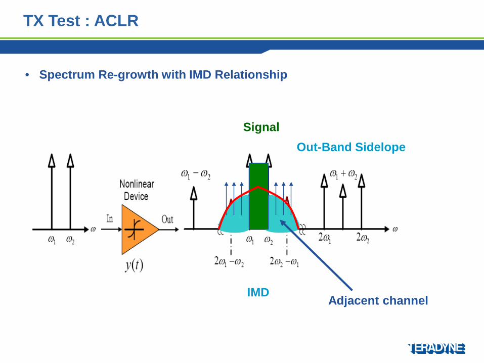
TX Test : ACLR
SignalOut-Band Sidelope
IMD Adjacent channel
• Spectrum Re-growth with IMD Relationship
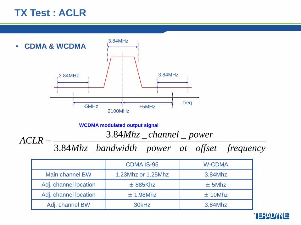
frequencyoffsetatpowerbandwidthMhzpowerchannelMhzACLR
_____84.3__84.3
=
freq+5MHz
3.84MHz
WCDMA modulated output signal
2100MHz-5MHz
3.84MHz3.84MHz
CDMA IS-95 W-CDMA
Main channel BW 1.23Mhz or 1.25Mhz 3.84Mhz
Adj. channel location ± 885Khz ± 5Mhz
Adj. channel location ± 1.98Mhz ± 10Mhz
Adj. channel BW 30kHz 3.84Mhz
• CDMA & WCDMA
TX Test : ACLR
TX Test : ACLR
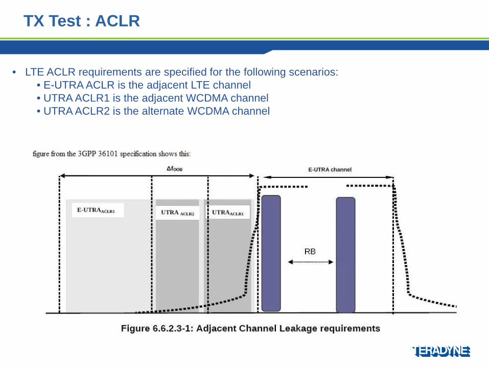
• LTE ACLR requirements are specified for the following scenarios:• E-UTRA ACLR is the adjacent LTE channel• UTRA ACLR1 is the adjacent WCDMA channel• UTRA ACLR2 is the alternate WCDMA channel
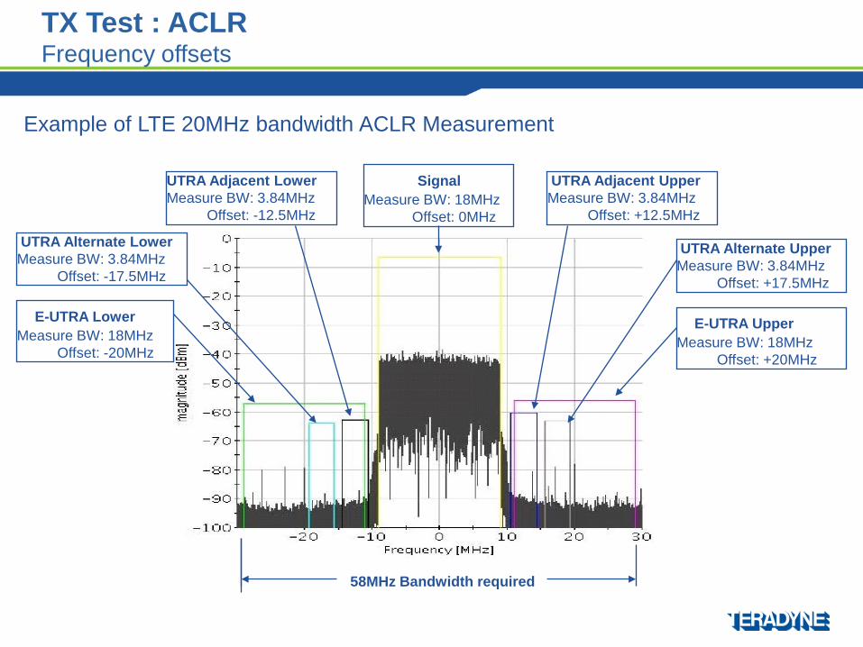
Example of LTE 20MHz bandwidth ACLR Measurement
SignalMeasure BW: 18MHz
Offset: 0MHz
E-UTRA UpperMeasure BW: 18MHz
Offset: +20MHz
UTRA Adjacent UpperMeasure BW: 3.84MHz
Offset: +12.5MHz
UTRA Alternate UpperMeasure BW: 3.84MHz
Offset: +17.5MHz
UTRA Adjacent LowerMeasure BW: 3.84MHz
Offset: -12.5MHz
UTRA Alternate LowerMeasure BW: 3.84MHz
Offset: -17.5MHz
E-UTRA LowerMeasure BW: 18MHz
Offset: -20MHz
58MHz Bandwidth required
TX Test : ACLR Frequency offsets
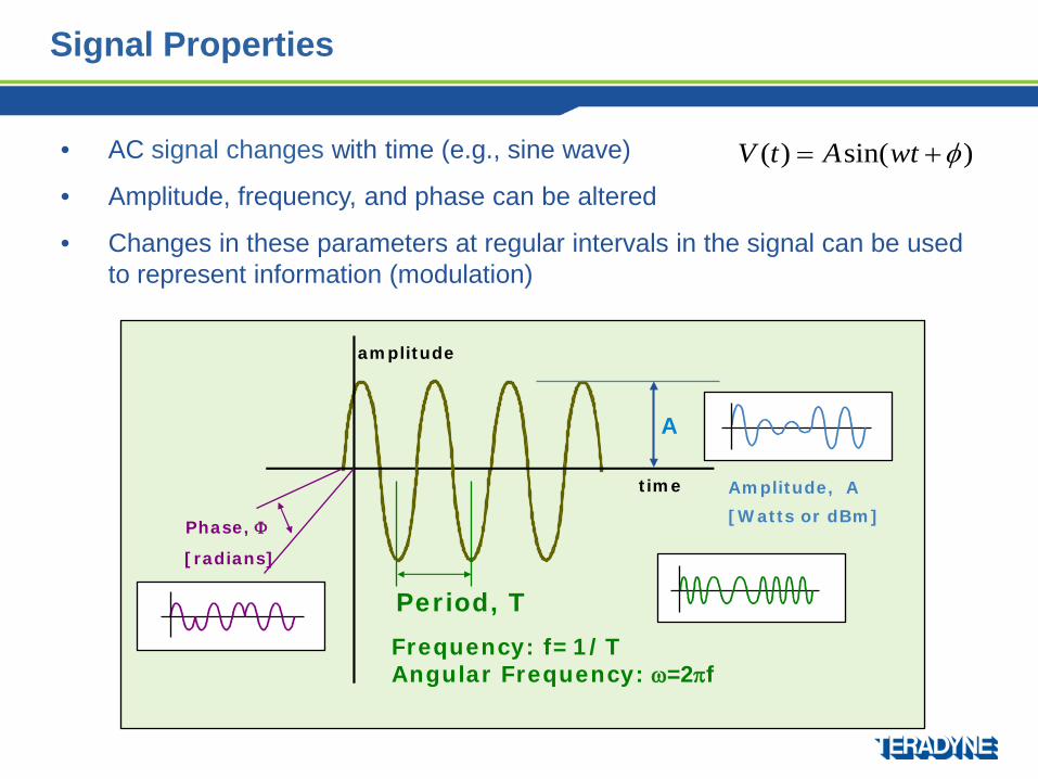
Signal Properties
Phase, Φ
[radians]
Amplitude, A[Watts or dBm]
Frequency: f=1/TAngular Frequency: ω=2πf
amplitude
time
A
Period, T
• AC signal changes with time (e.g., sine wave)
• Amplitude, frequency, and phase can be altered
• Changes in these parameters at regular intervals in the signal can be used to represent information (modulation)
)sin()( φ+= wtAtV
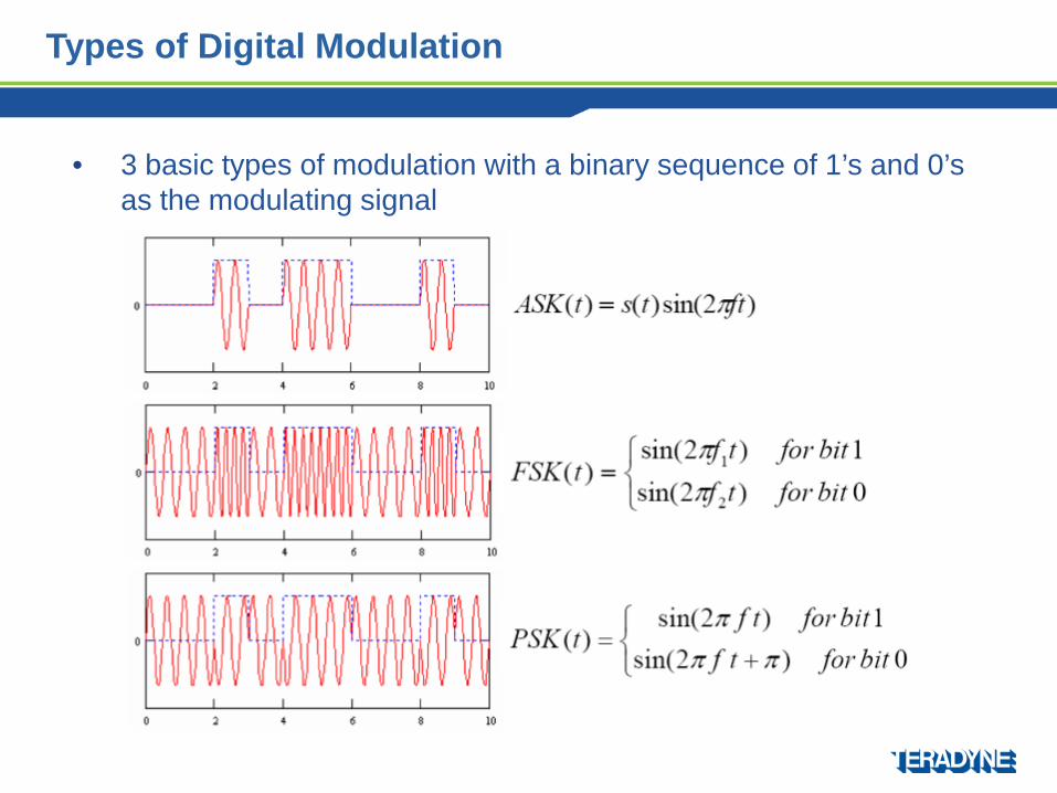
Types of Digital Modulation
• 3 basic types of modulation with a binary sequence of 1’s and 0’s as the modulating signal
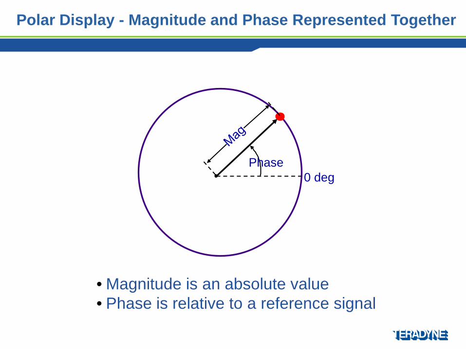
• Magnitude is an absolute value• Phase is relative to a reference signal
Phase0 deg
Polar Display - Magnitude and Phase Represented Together
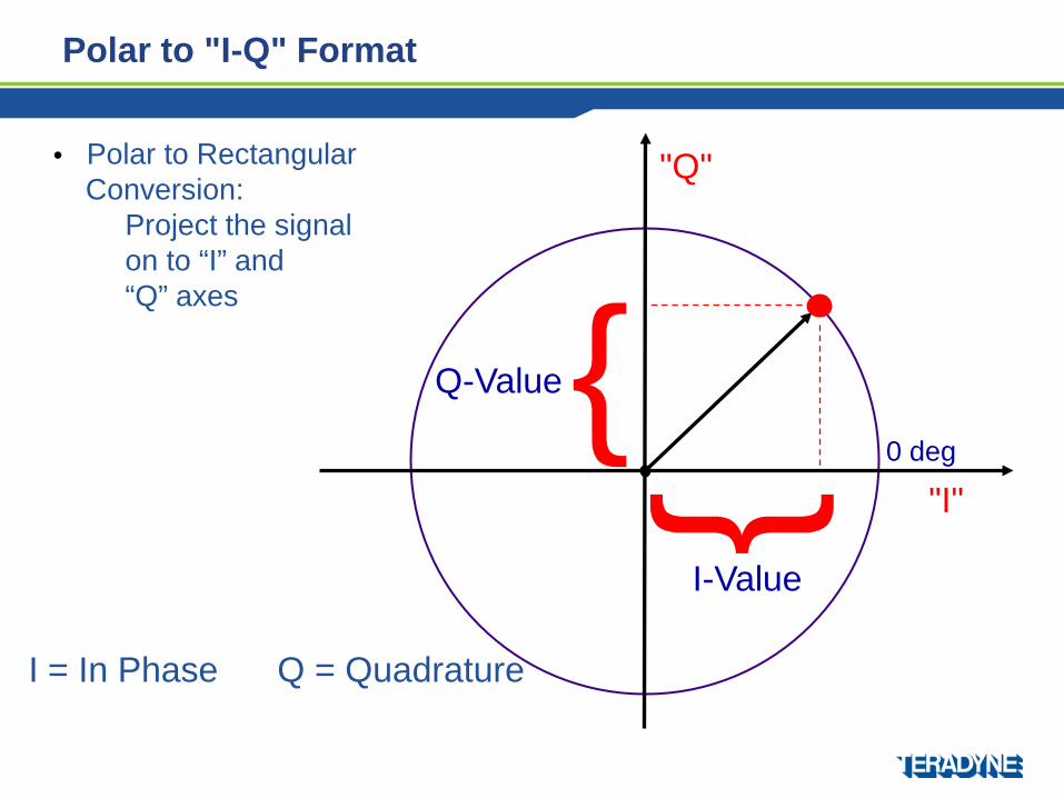
0 deg
"I"
"Q"
{Q-Value
{I-Value
• Polar to Rectangular Conversion:
Project the signalon to “I” and“Q” axes
Polar to "I-Q" Format
I = In Phase Q = Quadrature
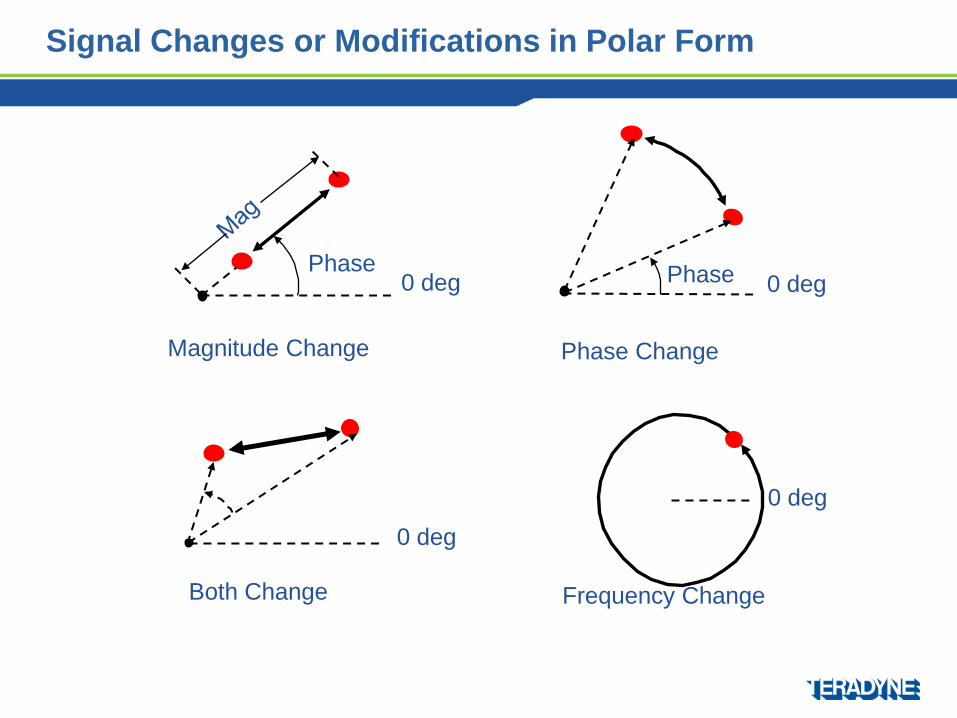
Magnitude Change Phase Change
Frequency ChangeBoth Change
Phase 0 degPhase
0 deg
0 deg0 deg
Signal Changes or Modifications in Polar Form
I and Q in a Radio Transmitter
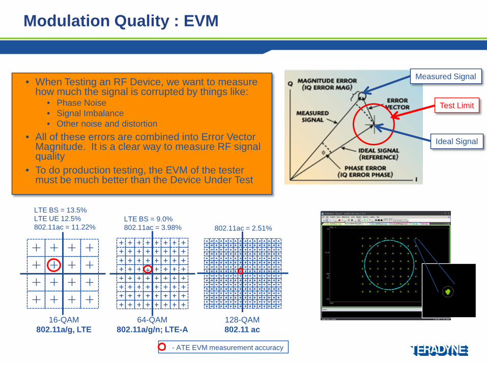
• When Testing an RF Device, we want to measure how much the signal is corrupted by things like:
• Phase Noise• Signal Imbalance• Other noise and distortion
• All of these errors are combined into Error Vector Magnitude. It is a clear way to measure RF signal quality
• To do production testing, the EVM of the tester must be much better than the Device Under Test
Ideal Signal
Measured Signal
Test Limit
LTE BS = 13.5%LTE UE 12.5%802.11ac = 11.22%
LTE BS = 9.0%802.11ac = 3.98% 802.11ac = 2.51%
16-QAM802.11a/g, LTE
64-QAM802.11a/g/n; LTE-A
128-QAM802.11 ac
- ATE EVM measurement accuracy
Modulation Quality : EVM
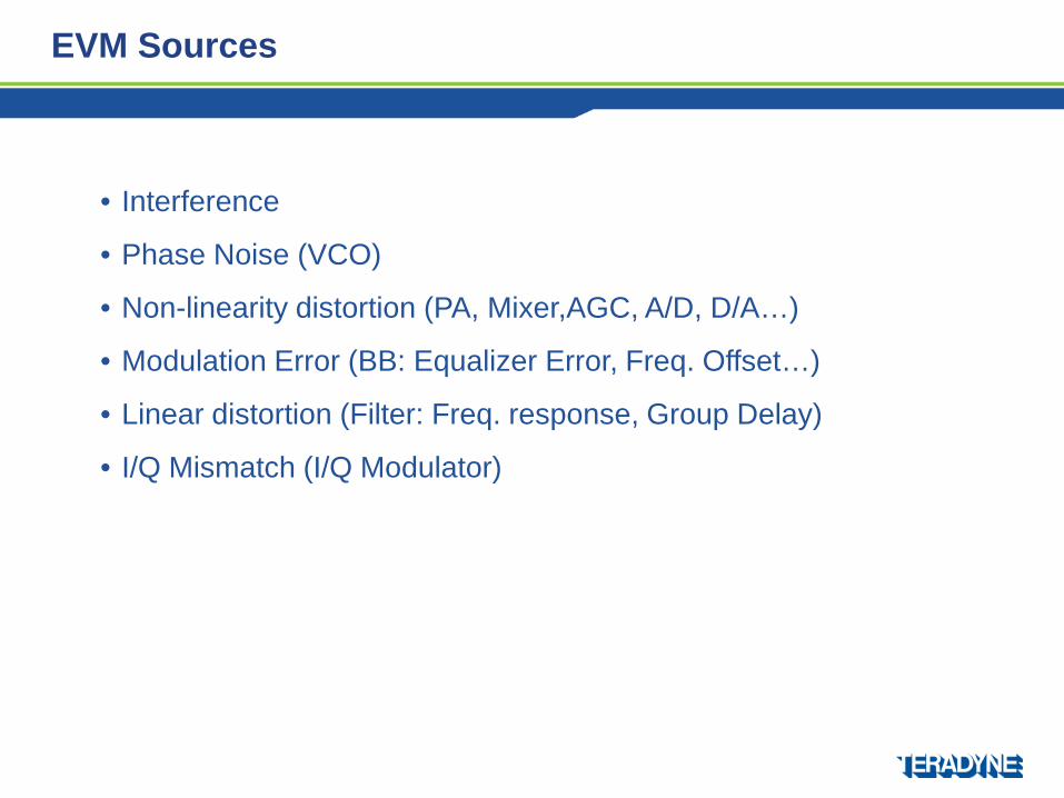
EVM Sources
• Interference
• Phase Noise (VCO)
• Non-linearity distortion (PA, Mixer,AGC, A/D, D/A…)
• Modulation Error (BB: Equalizer Error, Freq. Offset…)
• Linear distortion (Filter: Freq. response, Group Delay)
• I/Q Mismatch (I/Q Modulator)
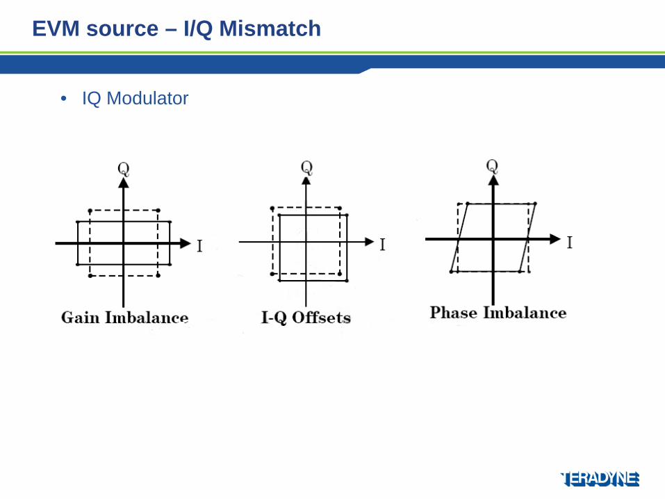
EVM source – I/Q Mismatch
• IQ Modulator
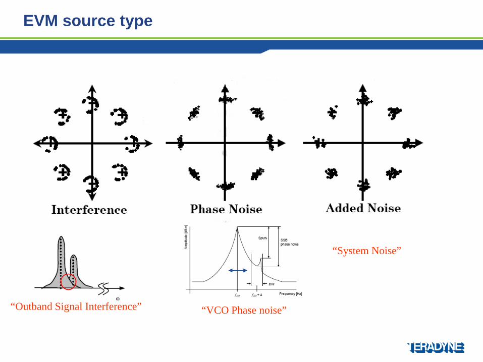
EVM source type
“VCO Phase noise”“Outband Signal Interference”
“System Noise”
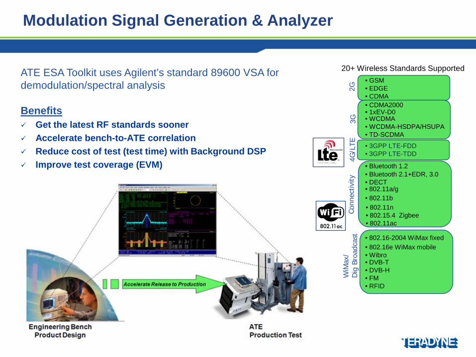
ATE ESA Toolkit uses Agilent’s standard 89600 VSA for demodulation/spectral analysis
Benefits Get the latest RF standards sooner Accelerate bench-to-ATE correlation Reduce cost of test (test time) with Background DSP Improve test coverage (EVM)
20+ Wireless Standards Supported• GSM
• WCDMA• WCDMA-HSDPA/HSUPA• TD-SCDMA
• Bluetooth 1.2• Bluetooth 2.1+EDR, 3.0• DECT• 802.11a/g• 802.11b
• EDGE• CDMA• CDMA2000• 1xEV-D0
• 802.11n• 802.15.4 Zigbee• 802.11ac
• 802.16-2004 WiMax fixed• 802.16e WiMax mobile• Wibro• DVB-T• DVB-H• FM• RFID
Conn
ectiv
ityW
iMax
/D
ig B
road
cast
3G2G
• 3GPP LTE-FDD • 3GPP LTE-TDD
4G/L
TE
Modulation Signal Generation & Analyzer
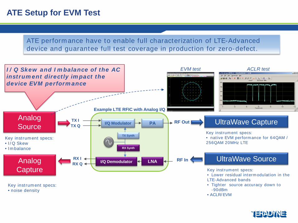
ATE Setup for EVM Test
TX ITX Q PA
RX IRX Q I/Q Demodulator LNA
Key instrument specs:• I/Q Skew• Imbalance
Key instrument specs:• native EVM performance for 64QAM / 256QAM 20MHz LTE
Example LTE RFIC with Analog I/Q
RF Out
RF In
ACLR testEVM test
Analog Source
Analog Capture
UltraWave Capture
UltraWave SourceKey instrument specs:• Lower residual intermodulation in the LTE-Advanced bands• Tighter source accuracy down to
-90dBm• ACLR/EVM
Key instrument specs:• noise density
ATE performance have to enable full characterization of LTE-Advanced device and guarantee full test coverage in production for zero-defect.
TX Synth
RX Synth
I/Q Modulator
Page 64
I/Q Skew and Imbalance of the AC instrument directly impact the device EVM performance
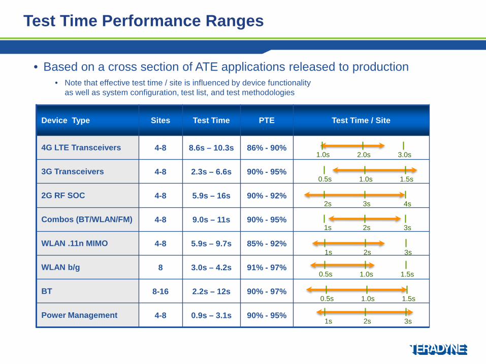
• Based on a cross section of ATE applications released to production• Note that effective test time / site is influenced by device functionality
as well as system configuration, test list, and test methodologies
Test Time Performance Ranges
Device Type Sites Test Time PTE Test Time / Site
4G LTE Transceivers 4-8 8.6s – 10.3s 86% - 90%
3G Transceivers 4-8 2.3s – 6.6s 90% - 95%
2G RF SOC 4-8 5.9s – 16s 90% - 92%
Combos (BT/WLAN/FM) 4-8 9.0s – 11s 90% - 95%
WLAN .11n MIMO 4-8 5.9s – 9.7s 85% - 92%
WLAN b/g 8 3.0s – 4.2s 91% - 97%
BT 8-16 2.2s – 12s 90% - 97%
Power Management 4-8 0.9s – 3.1s 90% - 95%
1.5s1.0s0.5s
1.5s1.0s0.5s
4s3s2s
3s2s1s
3s2s1s
1.5s1.0s0.5s
3s2s1s
3.0s2.0s1.0s

Questions