Embed Size (px)
Citation preview

RF INTEGRATED CIRCUITS: NOTES
UNIT-11. INTRODUCTION RF SYSTEMS – BASIC ARCHITECTURE:
The first and for most thing that it has is something called an antenna. This is the symbol for the
antenna. The cell phone has inside it an antenna. Now, there is a transmitter and there is a
receiver. So, there is a transmitter and there is a receiver; both are going to be using the same
antenna. How is it possible? How can both the transmitter and the receiver use the same antenna?
Now, for this, there is something called it is like a switch; it is called a duplexer. Now, this
switch separates the transmit path from the receive path. Duplexer is a surface acoustic wave
kind of component, that is why this duplexer has to be a very good duplexer – something that
separates the transmit chain from the receive chain; it could be a filter; in which case, it has to
have an extremely good isolation. It could be a switch maybe when the transmitter is working,
the receiver is not working. In that case also, it has to have very low attenuation; typically, it is a
semi-mechanical switch.
Let us look at the receiver side now, The first thing that you need is something called a low noise
amplifier, receiving a tiny signal from the atmosphere, this tiny signal has to be amplified, so that
you can make sense of what was spoken on the other side. So, it has got to be an amplifier,

Second thing is it has to be low noise. Low noise here means that, it does not add too much noise
on its own, A low noise amplifier does not add too much noise, Therefore, a low noise amplifier
cannot throw out the noise and keep the signal; it has to handle both the noise and the signal that
it has already received. Every system unless it is a passive lossless system, every other system
adds noise. If it burns power, it adds noise. So, a low noise amplifier is most probably going to
burn power; Just before throwing out the signal to the antenna to the duplexer, what we need is
something called a power amplifier, We want to blast as much power as possible into the
atmosphere, so that the base station can here me clearly. So, that is a power amplifier. That is the
last block on the transmit chain, let us try to understand that, a cell phone; when you are
receiving signal, it is probably going to use 800 megahertz or a 1600 megahertz or some
extremely high frequency. If it is an extremely high frequency, we do not like these extremely
high frequencies, because it is hard to work with them. So, the first thing that we need to do is to
bring it down to a lower frequency. So, how do we bring it down to a lower frequency? We use
something called a multiplier. Or, in other words, it is called a mixer. it down converts the high
frequency that you received to something that is more manageable, LO stands for local oscillator.
The local oscillator for the transmitter is typically different from the local oscillator of the
receiver, you do not want transmit and receive to be working at the same frequency band. So,
these two frequencies are generated on chip; they are different. And these two frequencies mix
with the RF signal or with the baseband signal and create the low frequency or the high
frequency whatever you want depending on Rx or Tx. the transmit side local oscillator will be
oscillating at a frequency different from the receive side local oscillator, Why cannot I transmit
and receive at the same frequency? Because if I do not have them different, then mostly, what I
am going to be hearing on the receive is an echo of what I transmitted.
2.TRANSMISSION MEDIA AND REFLECTIONS:-

an electromagnetic waveguide could be a wire; it could be a real waveguide; it could be the
atmosphere; could be anything, Gamma is the reflection coefficient. So, if there is a wave – it is
a waveguide; there is a wave hitting a certain object; a portion of the wave gets absorbed into the
object; a portion of the wave reflects back from the object. at the load, this reflection coefficient
is Z L minus Z 0 divided by Z L plus Z 0; where, Z L is basically R L in the case that I have
drawn; and Z 0 is the characteristic impedance of the waveguide in question. So, this is how we
are going to understand the reflections. So, the reflection coefficient happens to be equal to this.
At the source side, it is going to be something very similar – Z S minus Z 0 divided by Z S plus
Z 0; Z S in this case is the source resistance of the voltage that has been applied, the antenna is
passing over the signal to the low noise amplifier. If the low noise amplifier has an input
impedance of Z L; and if the antenna – receive antenna has the characteristic impedance of Z
naught; and if Z naught equal to Z l, then all the signal that hits the low noise amplifier is going
to be absorbed by the low noise amplifier; nothing of that signal is going to be reflected back, the
characteristics impedance of the antenna is chosen to be 50 ohms.

3. PASSIVE RLC NETWORKS:
3.1. INTRODUCTION:- One characteristic of R F circuits is the relatively large ratio of passiveto active components. In stark contrast with digital VLSI circuits (or even with other analogcircuits. such as op-amps), many of those passive components may be inductors or eventransformers, This chapter hopes to convey some underlying intuition that it is useful in thedesign of RLC networks. As we build up that intuition, we'll begin to understand the many goodreasons for the preponderance of RLC networks in RFcircuits. Among the mOSIcompelling ofthese are that they can be used to match or
Otherwise modify impedances (important for efficient power transfer. for example), canceltransistor parasitic to provide high gain at high frequencies and filler out unwanted signals. Tounderstand how RLC networks may confer these and other benefits. let's revisit some simplesecond-order examples from undergraduate introductory network theory. By looking a: howthese networks behave from a couple of different viewpoints .well build up intuition that willprove useful in understanding networks of much higher order.
3.2. PARALLEL RLC TANK: - Let's just jump right into the study of a parallel R LC circuit.As you probably know. This circuit exhibits resonant behavior: we'll see what this impliesmomentarily. This circuit is also often called a tank circuit \ (or simply tank), We begin bystudying its complex impedance. or more directly. its admittance (more convenient for a parallelnetwork: see Figure 1.1. For this network, we know that the admittance is simply
Figure 1.1 Parallel RLC network
Therefore say that. at very low frequencies. the network's admittance is essentially that of theinductor (since its admittance dominates the combination) and is also that of the capacitor at veryhigh frequencies. What divides "low" from "high" is the frequency at which the inductive andcapacitive admittances cancel. Known as the resonant frequency.this is given by
3.3. QUALITY FACTOR:-

specific about what stores or dissipates the energy. So. as we'll see later on, it applies perfectly
well even to distributed systems, such as microwave resonant cavities, where it is not possible to
identify individual inductances, capacitances, and resistances. It should also be clear that the
notion of Q applies both to resonant and nonresonant systems, so one may talk of the Q of an RC
circuit. A high-order system may exhibit multiple resonances, each with its own peak Q value.
From the fundamental definition, we also sec that the value we compute depends on whether or
not
we include external loading, and perhaps also on how that load connects to the network in
question. If we neglect the loading then we refer to the computed value as the unloaded Q, and if
we include it then we call it the loaded Q. whenever the context is ambiguous and the distinction
mailers. it is important to identify explicitly the type of Q under discussion.
Let's now use this definition to derive expressions for the Q of our parallel RLCcircuit at
resonance. At the resonant frequency, which we'll denote by Wo the voltage across the net work
is simply linR. Recall that energy in such a network sloshes back and forth between the inductor
and capacitor, with a constant sum at resonance. As a consequence then network energy and
power is given by
Then the Q of the network is given by
Where The quantity of √L/C is called characteristic impedance
3.4. SERIES RLC NETWORKS:- We may follow an exactly analogous dual approach to
deduce the properties of scries R LC circuits. The details of the derivations arc relatively
uninteresting. so here we simply present the relevant observations and equations.The resonant
condition corresponds again to the frequency where the capacitance and inductance cancel.

Rather than resulting in an admittance minimum, though. resonance here results in an impedance
minimum, with a value of R. The equation for Q involves the same terms as for the parallel case.
but in reciprocal form:
At resonance. the voltage across either the inductor or capacitor is Q times as great as that across
the resistor. Thus. if a series RLC network with a Q of 1000 is driven at resonance with a one-
volt source. then the resistor will have that one volt across it yet a thrilling one thousand volts
will appear across the inductor and capacitor.
3.5.OTHER RESONANT RLC NETWORKS :- Purely parallel or series R LC networks rarely
exist in practice. so it's important to take a look at configurations that might be more realistically
representative. Consider. for example. the case sketched in Figure 1.2. Because inductors tend to
be significantly lossier than capacitors. the model shown in the figure is often a more realistic
approximation to typical parallel RLC circuits. Since we've already analyzed the purely parallel
RLC network in detail. it would be nice if we could re-use as much of this work as possible. So,
let's convert the
Figure 1.2 not a quite parallel RLC circuits
circuit of Figure 3.2 to a purely parallel RLC network by replacing the series LR section with ,1
parallel one. Clearly. such a substitution cannot be valid in general. but over a suitably restricted
frequency range (e.g .. near resonance) the equivalence is pretty reasonable. To show this
formally. let 's equate the impedances of the series and parallel L R sections:

we may also derive a similar set of equations for computing series and parallel RC equivalents:
Let's pause for a moment and look at these transformation formulas, Upon closer examination.
it's clear that we may express them in a universal form that applies to both RC and LR networks:
where X is the imaginary part of the impedance. This way, one need only remember a single pair
of "universal" formulas in order to convert any "impure" RLC network into a purely parallel (or
series) one that is straightforward to analyze. However. One must bear in mind that/he
equivalences hold only over a narrow range of frequencies centered about W0.
3.6. RLC NETWORKS AS IMPEDANCE TRANSFORMERS:- The relative abundance of
power gain at low frequencies allows designers to treat it essentially as an infinite resource.
Design specifications are thus often expressed simply in terms of a voltage gain. for example,
without any explicit reference to or concern for power gain. Hence. circuit design at low
frequencies usually proceeds in blissful ignorance of the maximum power transfer theorem
derived in every undergraduate network theory course. In striking contrast with that insouciance.
RF circuit design is frequently preoccupied with power gain because of its relative scarcity.
Irnpedancc-rransforming networks thus play a prominent role in the radio frequency domain.
figure1.3 maximum power transfer
3.6.1 THE MAXIMUM POWER TRANSFER THEOREM :- To understand more explicitly
the value of impedance transformers. we now review the maximum power transfer theorem as

shown in Figure 1.3. The problem is this: Given a fixed source impedance Zs. what load
impedance ZL maximizes the power delivered to the load? The power delivered to the load
impedance is entirely due to RL. since reactive elements do not dissipate power. Hence. the
power delivered is simply
figure1.3 maximum power transfer
where VR and Vs are the rrnx voltages across the load resistance and source respectively. To
maximize the power delivered to RL. it's clear that XL and Xs should be inverses so that they sum
to zero. In addition. Maximizing above Eqn. under that condition leads to the result that RL
should equal Rs. Hence. the maximum power transfer from a fixed source impedance to a load
occurs when the load and source impedances are complex conjugates. Having established
mathematically the condition for maximum power transfer, we now consider practical methods
for achieving it .
3.6.2 THE L-MATCH :- The multiplication by Q of voltages or currents in resonant RLe
networks hints at their impedance-modifying potential. Indeed. the series-parallel RClLR
network conversion formulas developed in the previous section actually show this property
explicitly. To make this clearer. Consider once again the circuit of Figure 1.2. Redrawn slightly
as Figure 1.4. Here we treat Rs as a load resistance for the network. When this resistance is
viewed across the capacitor. it is transformed to an equivalent

1.4 Upward impedance transformer 1.5 Downward impedance transformer
R>>1 according to the formulas developed in the previous section. From inspection of those
"universal" equations. il is clear that Rp will always be larger them Rs. so the network of Figure
1.4 transforms resistances upward. To get a downward impedance conversion. just interchange
ports as shown in the Figure 3.5.
This circuit is known as an L-match because of its shape (perhaps you have to be lying on your
side and dyslexic to see this). and it docs have the attribute of simplicity. However, there are only
two degrees of freedom (one can choose only L and e).Hence. once the impedance
transformation ratio and resonant frequency have been specified, network Q is automatically
determined. If you want a different value of Q then you must use a network that offers additional
degrees of freedom: we'll study some of these shortly. As a final note on the L-match the
"universal" equations can be simplified if Q' >>l. If this inequality is satisfied. then the following
approximate equations hold is
Which may be written as
where Zo is the characteristic impedance of the network. One may also deduce that Q is
approximately the square root of the transformation ratio is given by
Finally. the reactance’s don't vary much in undergoing the transformation is

As long as Q is greater than about 3 or4. the error incurred will be under about 10%.If Q is
greater than 10. the maximum error will be in the neighborhood of 1% or 50.Hence. for quick.
Back-of-the-envelope calculations. these simplified equations are adequate. Final design values
can be computed using the full "universal" equations.
3.6.3 THE Pi-MATCH :- one limitation of the L-match is that one can specify only two of
center frequency. Impedance transformation ratio. and Q. To acquire a third degree of freedom.
one can employ the network shown in Figure 1.6.This circuit is known as a Pi -match, again
because of its shape. The most expedient way to understand this matching network is to view it
as two L matches connected in cascade. one that transforms down and one that transforms up;
see Figure 1.7. Here. the load resistance Rp is transformed to a lower resistance (known as the
image or intermediate resistance, here denoted R,) at the junction of the two inductances. The
image resistance is then transformed up to a value Rin by a second L-match section.
figure 1.6 The Pi match figure 1.7 The Pi match as cascaded of two L-matches
In order to derive the design equations. first transform the parallel RC subnetwork of the right-
hand L-section into its series equivalent. as shown in Figure 1.8, When we replace the output
parallel LC network with its series equivalent. the series resistance is. of course. R,. Hence. the Q
of the right-hand L-scction may be written as
Figure 1.8Pi-match with transformed right hand L-section.
At the same Time. recognize that the left-hand L section about series a resistance of R, at the
center frequency. Therefore. its Q is given by

The overall network of Q is given by
Above equation is allows us to find the image resistance. given Q and the transformation
resistances. Once R, is computed. the total inductance is quickly found is
The values of capacitances are given by
As a practical matter. note that finding Ri generally requires iteration. A good starting value can
be obtained by assuming that Q is large . In that case. Ri is approximately given by
If Q is very large, or if you're just doing some preliminary "cocktail napkin" calculations. then
iteration may not even be necessary. And that's all there is to it .As a parting note. one final bit of
trivial deserves mention. An additional reason that the Pi -match is popular is that the parasitic
capacitances of whatever connects to it can be absorbed into the network design. This property is
particularly valuable because capacitance is the dominant parasitic clement in many practical
cases.
3.6.4 THE T·MATCH :- The zr-march results from cascading two L-sections in one particular
way. Connecting up the L-sections another way leads to the dual of the Pi-match as shown in
Figure 1.9. Here what would be a single capacitor in a practical implementation has been
decomposed explicitly into two separate ones. The (parallel) image resistance is seen across
these capacitors. Either looking to the right or looking to the left as in the Pi-match.
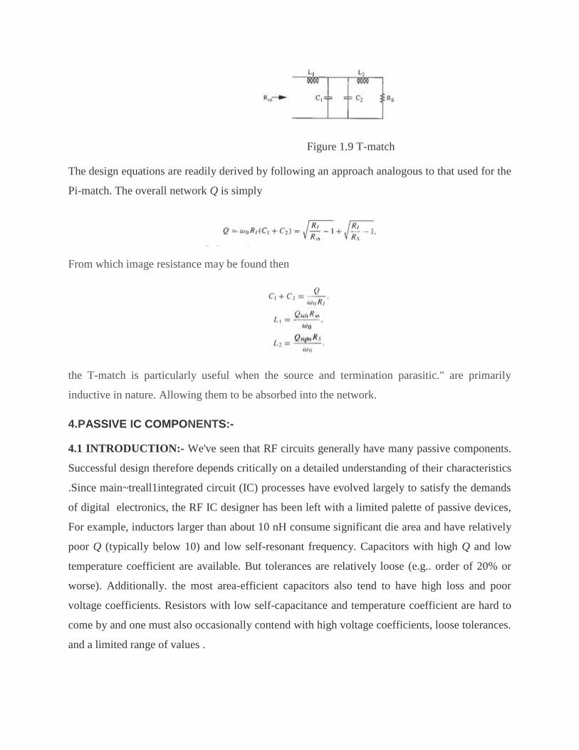
Figure 1.9 T-match
The design equations are readily derived by following an approach analogous to that used for the
Pi-match. The overall network Q is simply
From which image resistance may be found then
the T-match is particularly useful when the source and termination parasitic." are primarily
inductive in nature. Allowing them to be absorbed into the network.
4.PASSIVE IC COMPONENTS:-
4.1 INTRODUCTION:- We've seen that RF circuits generally have many passive components.
Successful design therefore depends critically on a detailed understanding of their characteristics
.Since main~treall1integrated circuit (IC) processes have evolved largely to satisfy the demands
of digital electronics, the RF IC designer has been left with a limited palette of passive devices,
For example, inductors larger than about 10 nH consume significant die area and have relatively
poor Q (typically below 10) and low self-resonant frequency. Capacitors with high Q and low
temperature coefficient are available. But tolerances are relatively loose (e.g.. order of 20% or
worse). Additionally. the most area-efficient capacitors also tend to have high loss and poor
voltage coefficients. Resistors with low self-capacitance and temperature coefficient are hard to
come by and one must also occasionally contend with high voltage coefficients, loose tolerances.
and a limited range of values .

4.2 INTERCONNECT AT RADIO FREQUENCIES: SKIN EFFECT
At low frequencies, the properties of interconnect we care about most are resistivity, current-
handling ability, and perhaps capacitance. As frequency increases. we find that inductance might
become important. Furthermore, we invariably discover that the resistance increases owing to a
phenomenon known as the skill effect.
Skin effect is usually described as the tendency of current to now primarily on the surface (skill)
of a conductor as frequency increases. Because the inner regions of the conductor are thus less
effective at carrying current than at low frequencies, the useful cross-sectional area of a
conductor is reduced. thereby producing a corresponding increase in resistance.
To develop a deeper understanding of the phenomenon. we need to appreciate explicitly the role
of the magnetic field in producing the skin effect. To do so qualitatively. let's consider a solid
cylindrical conductor carrying a time-varying current, as shown in Figure 4.1. Assume for now
that the return current (there must always be one in any real system) is far enough away that its
influence may be neglected. A time varying current I generate a time-varying magnetic field H.
That lime-varying field induces a voltage around the rectangular path shown. in accordance with
Faraday's law. Ohm's law then tells us that the induced voltage in turn produces a current flow
along that same rectangular path. as indicated by the arrows. Now here's the key observation:
The direction of the induced current along path A is opposite that along8. The induced current
thus adds to the current flowing along one side of the rectangle and subtracts from the other.
Taking care to keep track of algebraic signs. We see that the current along the surface is the one
that is augmented whereas the current below the surface is diminished. In other words. current
flow is strongest near the surface; that's the skin effect
figure 4.1. Illustration 01 skin effect with isolated cylindrical conductor

To develop this idea a little more quantitatively. let's apply Kirchhoff's voltage law (with proper
accounting for the induced voltage term. both in magnitude and sign) around the rectangular path
to obtain
where J is the current density. p is the resistivity. and ¢. the flux. is perpendicular to the rectangle
shown.We see that. as deduced earlier. the current density along path A is indeed larger than
along 8 by an amount that increases as either the depth, frequency. or magnetic field strength
increases and also as the resistivity decreases. Any of these mechanisms acts to exacerbate the
skin effect. Furthermore. the presence of the derivative tells us that the current undergoes more
than a simple decrease with increasing depth; there is a phase shift as well.
if we now increase the radius of curvature to infinity. we may convert the cylinder into the
rectangular structure that is more commonly analyzed to introduce skin effect; sec Figure 4:2.
We will provide only {he barest outline of how to set up the problem. and then Simply present
the solution. Computing the voltage induced by H around the rectangular contour proceeds th
Kirchhoff's voltage law is given by
Figure 4.2. Subsection of semi 'infinite conductive block.

here the subscript 0 denotes the value at the surface of the conducting block... Now express land
H (and thus B) explicitly as sinusoidally time-varying quantities. Based on this we can states the
equation of skin effects is given by
Notice that the current density decays exponentially from its surface value, Notice also (from the
second exponential factor) that there is indeed a phase shift. as argued earlier, with a l-rad lag at
a depth equal to δ.
For this case of an infinitely wide. Infinitely long. and infinitely deep conductive block. the skin
depth is the distance below the surface at which the current density has dropped by a factor of e.
For copper at I GHz. the skin depth is approximately211m. For aluminum. that number increases
a little bit. to about 2.5 urn. What this exponential decay implies is that making a conductor
much thicker than a skin depth provides negligible resistance reduction because the added
material carries very little current. Furthermore. we may compute the effective resistance as that
of a conductor of thickness li in which the current density is uniform. This fact is often used to
simplify computation of the AC resistance of conductors. To make sure that the result is valid.
however. the boundary conditions must match those used in deriving our system of equations:
The return currents must be infinitely far away. and the conductor must resemble a semi-infinite
block. The latter criterion is satisfied reasonably well if all radii of curvature, and all thicknesses.
are at least 3-4 skin depths.
4.3 RESISTORS:- are relatively few good resistor options in standard CMOS (complementary
metal-oxide silicon) processes. One possibility is to use polysilicon poly interconnect material.
Since it is more resistive than metal. However, most poly these days is solicited specifically to
reduce resistance. Resistivity’s tend to be in the vicinity of roughly S-IO ohms per square (within
a factor of about 2-4. usually). so poly is appropriate mainly for moderately small-valued
resistors. Its tolerance is often poor (e.g., 35%), and the temperature coefficient, defined as

depends on doping and composition and is typically in the neighborhood of 1000ppm/°C.
Unsolicited poly has a higher resistivity (by approximately an order of magnitude, depending on
doping), and the TC can vary widely (even to zero, in cer tain cases) as a function of processing
details. It is usually not tightly controlled. So unsolicited poly, if available as an option at all.
Frequently Possesses very loose tol erances (e.g., 50%). Advanced bipolar technologies use self-
aligned poly emitters, so poly resistors are an option there, too. In addition to their moderate TC.
poly resistors have a reasonably low parasitic ca pacitance per unit area and the lowest voltage
coefficient of all the resistor materials available in a standard CMOS technology, Resistors
made from source-drain diffusions are also an option. The resistivity’s and temperature
coefficients are generally similar (within a factor of 2, typically) to those of solicited poly
silicon, with lower TC associated with heavier doping. There is also significant parasitic
(junction) capacitance as well as a noticeable voltage co efficient. The former limits the useful
frequency range of the resistor, while the latter limits the dynamic range of voltages that may be
applied without introducing sig nificant distortion. Additionally, care must be taken to avoid
forward-biasing either end of the resistor. These characteristics usually limit the use of diffused
resistors to noncritical circuits.In modern VLSI (very large-scale integration) technologies.
source-drain "diffusions" arc defined by ion implantation. The source-drain regions formed in
this way are quite shallow (usually no deeper than about 200-300 nrn, scaling roughly with
channel length), quite heavily doped, and almost universally silicided, leading to moderately low
temperature coefficients (order of SOO-IOOO ppm/oC).Wells may be used for high-value
resistors. since resistivities are typically in the range of 1-10 kQ per square. Unfortunately, the
parasitic capacitance is substantial because of the large-area junction formed between the well
and the substrate; the resulting resistor has poor initial tolerance (±SO-80%), large temperature
coefficient (typically about 3000-S000 ppm/oC. owing to the light doping). and large voltage
coefficient. Well resistors must therefore be used with care.Sometimes, a MOS transistor is used
as a resistor, even a variable one. With a suitable gate-to-source voltage. a compact resistor can
be formed. From first-ordertheory, recall that the incremental resistance of a long-channel MOS
transistor in the triode region is

Unfortunately, implicit in this equation is that a MOS resistor has loose tolerance (because it
depends on the mobility and threshold), high temperature coefficient (because of mobility and
threshold variation with temperature) and is quite nonlinear (because it depends on VDS). These
characteristics frequently limit its use to noncritical circuits outside of the signal path. An
exception is use of such a resistor in certain gain control applications in which the gate drive is
derived from a feedback loop so that variations in device characteristics are automatically
compensated.One other option that is occasionally useful, particularly to prevent thermal runway
in bipolar power stages with paralleled devices. is to use metal interconnect asa small resistor. In
most interconnect technologies, metal resistivities are usually onthe order 01SOmQ /square, so
resistances up to around 10 Q are practical.Aluminum is most commonly used in interconnect
and has a temperature coefficient of about 3900 ppm/°C. The TC varies little with temperature
and the resistance may be considered PTAT (proportional 10 absolute temperature) over the
military temperature range (-SSOC to 125°C) to a reasonable approximation is
where one data point, the resistance Roat temperature To, is known.Some processes offer one or
more layers of interconnect made of some silicide(mainly for its superior electrornigrution
properties). The resistivity is about an order of magnitude larger than that of pure aluminum or
copper, while the TC is about the same.A few companies that specialize in analog circuits have
modified their processes to provide excellent resistors, such as those made ofNiCr(nichrome) or
SiCr (sichrome). These resistors possess low TC (order of 100 ppm/oC or Jess). and thin-film
versions arc easily trimmed with a laser to absolute accuracies better than a percent.
Unfortunately, these processes are not universally available. and the additional process steps
increase die cost significantly.
4.4 CAPACITORS:- the interconnect layers may be used to make traditional parallel plate
capacitors as shown in figure 4.8 However ordinary interlevel dielectric tends to be rather thick
(order of 0.5-1 lim). precisely 10 reduce the capacitance between layers. so the capacitance per
unit area is small (a typical value is 5 x 10⁻⁵ pF/J..I.m2). Additionally .one must be aware of the
capacitance formed by the bottom plate and any conductors (especially the substrate) beneath it.

This parasitic bottom plate capacitance is frequently as large as 1O-30o/c (or more) of the main
capacitance and often severely limits circuit performance.
Figure 4.8 paralle plate capacitor
The standard capacitance formula is given by
Somewhat underestimates capacitance because it does not take fringing into account. but it is
accurate as long as the plate dimensions are much larger than the plate separation H. In cases
where this inequality is not well satisfied. a rough first-order correction for the fringing may be
provided by adding between H and 2H to each of W and L in computing the area of the plates,
Choosing the maximum yields
One of the few bits of good news in IC passive components is that the TC metal capacitors are
quite low. Usually in the range of approximately 30-50 ppm/f'C.and is dominated by the TC of
the oxide's dielectric constant itself. as dimensional variations with temperature are negligible.
A simple structure that illustrates the general idea is shown in Figure 4.9, where th two terminals
of the capacitor are distinguished by different shadings. As can be seen. the "top" and "bottom"
plates. constructed out of the same metal layer. Alternate to exploit the lateral flux. Ordinary
vertical flux may also be exploited by arranging the segments of a different metal layer in a
complementary pattern, as shown in figure 4.10.

figure 4.9 example of lateral flux capacitor (top-view) figure 4.10 example of lateral fluxcapacitor (side-view)
An important attribute of a lateral flux capacitor is that the parasitic bottom plate capacitance IS
much smaller than for an ordinary parallel plate structure, since it consumes less area for a given
value of total capacitance. In addition, adjacent plates help steal flux away from the substrate,
further reducing bottom plate parasitic capacitance, as seen in Figure 4.11.
4.5 INDUCTORS:- From the point of view of R F circuits. the lack of a good inductor is by far
the most conspicuous shortcoming of standard Ie processes. Although active circuits can
sometimes synthesize the equivalent of an inductor. they always have higher noise. distortion,
and power consumption than "real" inductors made with some number of turns of wire.
4.5.1. SPIRAL INDUCTORS:- The most widely used on-chip inductor is the planar spiral,
which can assume many shapes as shown in Figure 412. The choice of shape is more often made

on the basis of convenience (e.g., whether the layout tool accommodates non-Manhattan
geometries) or habit than anything else. Despite stubborn lore 10 the contrary. the inductance and
Q values attainable are very much second-order functions of shape, so engineers should feel free
to usc their favorite shape with relative impunity. Octagonal or circular spirals are moderately
better than squares (typically on the order of 10'70)and hence arc favored when layout tools
permit their use - or when that modest difference represents the margin between success and
failure, The most common realizations use the topmost metal layer for the main part of the
inductor (occasionally with two or more levels strapped together to reduce resistance) and
provide a connection to the center of the spiral with a cross under implemented with some lower
level of meta\. These conventions arise from quite practical considerations: the topmost metal
layers in an integrated circuit are usually the thickest and thus generally the lowest in resistance.
Furthermore. maximizing the distance to the substrate minimizes the parasitic capacitance
between the inductor and the substrate.
Figure 4.12 planar spiral inductors
the inductance of an arbitrary spiral is a complicated function of geometry, and accurate
computations require the use of field solvers or Greenhouse's method." However, a (very) crude
zeroth-order estimate. suitable for quick hand calculations, is

where L is in henries, II is the number of turns. and r is the radius of the spiral in meters. This
equation typically yields numbers on the high side, but generally within 30% of the correct value
(and often better than that).For shapes other than square spirals, multiply the value given by the
square spiral formula by the square root of the area ratio to obtain a crude estimate of the correct
value Thus. for circular spirals, multiply the square-spiral value by (π/4)0.5 ~ 0.89, and by 0.91
for octagonal spirals. Perhaps more useful for the approximate design of a square spiral inductor
is the following equation is
where P is the winding pitch ill turns/meter: wc have assumed that the permeability is that of free
space. The first of these. which applies to a hollow square spiral inductor is shown in figure 4,22
is
where dout is the outer diameter and davg is the arithmetic mean of the inner and outer
diameters. Checks with a field solver reveal that this modified Wheeler formulae exhibits errors
below 5% for typical IC inductors. The inductance of planar spirals of all regular shapes can be
cast in a simple unified form if we base a derivation on the properties of a uniform current sheet
is
here p is the fill factor, defined as
Figure 4.13 shows a relatively complete model for on-chip spirals. 17 The model is symmetrical.
even though actual spirals are not. Fortunately. the error introduced is negligible in most
instances. An estimate for the series resistance may be obtained from the following equation is

Figure 4.14 model for on-chip inductors


![Call Me Impure [Gumucio]](https://img.pdfslide.net/doc/110x75/5535bacc550346a20b8b46e4/call-me-impure-gumucio.jpg)