Embed Size (px)
Citation preview
Project Number: REL - 7778
RF POWER AMPLIFIER CHARACTERIZATION FOR PREDISTORTION LINEARIZATION
By
Tarra Epstein
Christopher Serrano
Date: May 1, 2007
Major Qualifying Project Report submitted to the Faculty of
WORCESTER POLYTECHNIC INSTITUTE
in partial fulfillment of the requirements for the degree of
Bachelor of Science
Approved:
Professor Reinhold Ludwig
_____________________________ Professor John McNeill

Table of Contents List of Figures.......................................................................................................................... 2 List of Tables ........................................................................................................................... 4 Abstract.................................................................................................................................... 5 1 Introduction..................................................................................................................... 6 2 Background ..................................................................................................................... 8
2.1 Power Amplifier Linearity........................................................................................ 8 2.1.1 Gain Compression and Phase Shift................................................................... 9 2.1.2 Intermodulation Distortion.............................................................................. 11
2.2 Typical PAs and Applications ................................................................................ 14 2.2.1 RF PA Circuitry Design Considerations......................................................... 14 2.2.2 PA Use in Cellular Phones.............................................................................. 15 2.2.3 PA Use in Base Stations ................................................................................. 16 2.2.4 PA Use in Wireless LANs .............................................................................. 18 2.2.5 Current PA Power Reduction Techniques ...................................................... 19
2.3 Digital Modulation Schemes................................................................................... 20 2.3.1 Phase Shift Keying.......................................................................................... 20 2.3.2 Quadrature Amplitude Modulation................................................................. 21
2.4 Literature Review and Prior Art ............................................................................. 23 2.4.1 Analog Schottky Diode Predistortion ............................................................. 23 2.4.2 Feedforward Linearization.............................................................................. 26 2.4.3 Cartesian Feedback Linearization................................................................... 27 2.4.4 Digital Adaptive Predistortion ........................................................................ 28 2.4.5 Non-adaptive Predistortion Algorithm ........................................................... 30
3 Software: Predistorter and Pattern Generator.......................................................... 32 3.1 MATLAB Predistorter ............................................................................................ 32 3.2 FPGA Pattern Generator ......................................................................................... 33
4 Hardware Implementation........................................................................................... 34 4.1 Transmitter.............................................................................................................. 34 4.2 Power Amplifier...................................................................................................... 37 4.3 Receiver .................................................................................................................. 40
5 Results ............................................................................................................................ 42 5.1 Simulation Results Using ADS Model of ZHL-42W PA....................................... 42 5.2 PA Characterization ................................................................................................ 48 5.3 Simulation Results Using S-parameter Measurements........................................... 52 5.4 Hardware Results .................................................................................................... 56
Conclusions and Recommendations.................................................................................... 61 Acknowledgements ............................................................................................................... 63 Appendix A: MATLAB Code .............................................................................................. 64 Appendix B: MATLAB Code from Previous MQP........................................................... 72 Appendix C: VHDL Pattern Generator Code.................................................................... 82 References.............................................................................................................................. 85
1

List of Figures Figure 1 - Gain compression of a PA...................................................................................... 10 Figure 2 - PA phase advance in response to input power. ...................................................... 11 Figure 3 - Odd-order intermodulation distortion products. .................................................... 12 Figure 4 - Third order intercept point (IP3). ........................................................................... 13 Figure 5 - Power amplifier matching network schematic....................................................... 15 Figure 6 - Typical CDMA phone power amplifier. ................................................................ 16 Figure 7 - A DS1847 controls the gate voltage of the LDMOS amplifier.............................. 17 Figure 8 - DS1847 Temperature conversion hysteresis.......................................................... 18 Figure 9 - P35-4712-1 IC single chip transceiver................................................................... 19 Figure 10 - 16-QAM constellation diagram............................................................................ 21 Figure 11 - QAM transmitter. ................................................................................................. 22 Figure 12 - QAM receiver....................................................................................................... 23 Figure 13 - Predistorter conceptual diagram........................................................................... 23 Figure 14 - Schottky diode open-loop predistortion circuit.................................................... 24 Figure 15 - Magnitude of forward voltage gain versus RD in Shottky diode predistortion .... 25 Figure 16 - Phase of forward voltage gain versus RD in Shottky diode predistortion ............ 25 Figure 17 - Feedforward linearization circuits........................................................................ 26 Figure 18 - Typical Cartesian feedback system...................................................................... 28 Figure 19 - Predistortion algorithm block diagram................................................................. 31 Figure 20 - MATLAB predistorter block diagram. ................................................................ 32 Figure 21 - FPGA pattern generator block diagram. .............................................................. 33 Figure 22 - Hardware system overview. ................................................................................. 34 Figure 23 - Test hardware transmitter module........................................................................ 35 Figure 24 - Xilinx Spartan-3 FPGA........................................................................................ 35 Figure 25 - LabView software for DAC configuration .......................................................... 36 Figure 26 - Analog Devices AD9777 DAC and AD8349 modulator..................................... 37 Figure 27 - Hittite Microwave HMC308 with evaluation board ............................................ 38 Figure 28 - Hittite Microwave HMC474 with evaluation board ............................................ 39 Figure 29 - Fundamental and third harmonic output of ADS simulation for the ZHL-42W.. 39 Figure 30 - Test hardware receiver module. ........................................................................... 40 Figure 31 - Analog Devices AD8347 demodulator ................................................................ 41 Figure 32 - ADS Simulation of ZHL-42W output spectrum at 900MHz. .............................. 42 Figure 33 - ADS Simulation of ZHL-42W output spectrum at 1960 MHz. ........................... 43 Figure 34 - AM-AM and AM-PM charts based on the ADS ZHL-42W model..................... 44 Figure 35 - Simulation of ZHL-42W PA response without predistortion, without noise. ..... 45 Figure 36 - Simulation of ZHL-42W PA response with predistortion, without noise............ 46 Figure 37 - Simulation of ZHL-42W PA response without predistortion, with noise............ 47 Figure 38 - Simulation of ZHL-42W PA response with predistortion, with noise................. 47 Figure 39 - Simulated predistorter effectiveness using ZHL-42W PA................................... 48 Figure 40 - Gain compression of HMC308 amplifier with a 3.3V supply. ............................ 49 Figure 41 - Gain compression of HMC308 amplifier with a 5V supply. ............................... 50 Figure 42 - Gain compression of HMC474 amplifier with a 3.3V supply. ............................ 50 Figure 43 - Gain compression of HMC474 amplifier with a 5V supply. ............................... 51 Figure 44 - Gain compression of ZHL-42W amplifier........................................................... 51 Figure 45 - ZHL-42W received signal without predistortion. ................................................ 53
2

Figure 46 - ZHL-42W received signal after predistortion ...................................................... 53 Figure 47 - Signal constellation for ZHL-42W predistortion. ................................................ 54 Figure 48 - Predistortion effectiveness plot for HMC308. ..................................................... 55 Figure 49 - Predistortion effectiveness plot for HMC474. ..................................................... 55 Figure 50 - FPGA output. ....................................................................................................... 56 Figure 51 - DAC output viewed at 500kS/s............................................................................ 57 Figure 52 - Modulator output.................................................................................................. 58 Figure 53 - PA output after attenuation. ................................................................................. 58 Figure 54 – Voltage versus time IMXO output of demodulator............................................. 59 Figure 55 – Voltage versus time QMXO output of demodulator. .......................................... 60
3

List of Tables Table 1 - Power consumption in a GSM cellular phone......................................................... 15 Table 2 - AM-AM and AM-PM Table based on the ADS ZHL-42W PA model .................. 44
4

Abstract The purpose of this Major Qualifying Project was to develop and evaluate a digital baseband
predistortion approach for radio frequency power amplifiers (RFPA). We also aimed to
develop a hardware implementation of the system. The predistorter implements a look-up-
table (LUT) to restore a baseband signal constellation and is simulated using actual RFPA
characteristics. The testing includes the use of MATLAB, a Xilinx Spartan-3 FPGA as a
pattern generator, a digital-to-analog converter (DAC), a modulator, an RFPA, and a
demodulator.
5

1 Introduction
As technology advances in areas such as communication systems, so does power
amplifier (PA) linearity requirements. There is an increasing demand for faster data
transmission, which demands higher bitrates. When the bitrate of a signal increases within
its finite bandwidth, the transmission of the signal is more prone to errors. Problems are
further complicated due to the fact that PAs are intrinsically nonlinear, which leads to
distortion of the transmitted signals. Therefore, PA linearization is an area of importance in
data transmission [1]. Many linearization techniques have been explored, but some have
proven more effective than others.
Analog Diode Predistortion is a simple and inexpensive predistortion technique that
relies on a diode’s gain expansion and phase lag. This method does not take into account
aging and temperature effects, and the PA characteristics must be known beforehand.
Feedforward linearization is a method consisting of two closed loops. Unfortunately, this
method requires the PA to be very linear. Another simple, common linearization method is
Cartesian feedback linearization, which employs two feedback loops separately for the in-
phase (I) and quadrature (Q) signals. A disadvantage of this method is the bandwidth
limitation. The method of linearization implemented in this project is digital predistortion.
This technique has the advantage of adapting to PA characteristics that change over time due
to temperature or aging. It also has the ability to linearize amplifier output up to the full
saturation level of the amplifier [1].
The designed predistorter runs on a PC in MATLAB and creates a look-up-table
(LUT) derived from either an Agilent Advanced Design System (ADS) model or S-parameter
measurements of a PA. We used the LUT to determine what input magnitude and phase to
the PA is required to obtain the desired, ideal output. We ran simulations in MATLAB to
verify the effectiveness of the predistortion algorithm using S-parameter measurements
obtained with the Agilent E8363B network analyzer. With these measurements, we adjusted
the predistortion algorithm to fit the various PA characteristics.
6

We programmed a Xilinx Spartan-3 FPGA to output the predistorted signal to our
hardware test equipment. The equipment included the use of an AD9777 digital-to-analog
converter (DAC) with an AD8349 modulator as a transmitter. We used three PAs for the
testing of the predistorter: Mini-Circuits ZHL-42W, Hittite Microwave HMC308, and Hittite
Microwave HMC474. The system receiver consisted of an attenuator and an AD8347
demodulator. We verified the output of each piece of hardware used in the setup and
measured the demodulator output using an oscilloscope.
7

2 Background In this section, we discuss the characteristics of power amplifiers (PAs) that affect the
linearity of amplified signals. We also discuss typical uses of PAs and the problems faced
with each application. We explain the modulation scheme we used in this project, and we
explore existing predistortion schemes and discuss the shortcomings of each. Finally, we
discuss the concept of our predistortion process.
2.1 Power Amplifier Linearity
Linearity is a critical characteristic of an RF power amplifier (PA). Linearity of a PA
is dependent on its conduction angle, the fraction of the signal cycle during which current
flows through the load. Based on this conduction angle, power amplifiers are categorized in
four essential classes: A, B, AB, and C.
In class A amplifiers, current flows constantly through the load, resulting in a
conduction angle of 360°. Though a class A amplifier’s performance is very linear, its power
efficiency is the poorest of the four classes of power amplifiers at 50 percent. Amplifier
efficiency, η , is defined by (1), dependent on the conduction angle, Θ. Class A amplifiers
are most commonly used in small-signal applications where the benefits of linearity outweigh
the downfalls of inefficiency [2].
sin
2[ cos( ) 2sin( )]2 2
η Θ − Θ=
Θ ΘΘ −
(1)
Class B amplifiers bias the PA near the cutoff, producing a conduction angle of 180°.
This means current flows only half of the RF cycle, and the efficiency of these amplifiers is
greater than class A amplifiers at 78.5 percent. The downside to this efficiency is waveform
distortion that takes place, adversely affecting linearity and weakening performance [2].
Class AB amplifiers allow current to flow as necessary, and their conduction angle is
between 180° and 360°. Any bias point between these two angles can be selected, resulting
in low-distortion, low-efficiency operation; high–distortion, high efficiency operation; or
8

anywhere in-between. Class AB amplifiers are commonly used in Single Side Band (SSB)
linear amplifier applications [2].
Class C amplifiers bias the PA beyond cut-off, and waveforms can be vastly
distorted. Efficiency for these amplifiers is very high, however, at about 90 percent [2].
Class C amplifiers’ non-linearity makes them unacceptable for AM or SSB signal
amplification [2].
The conduction angle of an amplifier has an inverse relationship with the gain
compression and intermodulation distortion (IMD) of the amplifier output. Amplifiers with a
large conduction angle experience the least gain compression and IMD, while amplifiers with
a small conduction angle (180° or below) experience significant gain compression and IMD.
These two amplifier nonlinearities will be discussed in this section. An ideal amplifier has a
perfectly linear transfer characteristic. This means that the gain of the amplifier is not
dependant on input frequency and does not increase or decrease as the input voltage changes,
causing no gain compression [3].
2.1.1 Gain Compression and Phase Shift
Gain compression in an amplifier is defined as a reduced gain due to the nonlinear
transfer function of the amplifier. This nonlinearity can be caused by power dissipation or by
overdriving the amplifier with a large input power, driving it past its linear region. As the
input power to an amplifier is increased beyond the amplifier’s linear region, the gain is
reduced and causes a nonlinear increase in output power. A graphical explanation of this
compression can be seen in Figure 1 [4] where the output power reaches saturation when the
input exceeds a certain power level.
9

Figure 1 - Gain compression of a PA occurs when the device is driven past its linear region [4].
Gain compression proves a problem when driving an amplifier with a high input
power signal. In the compression region, the output of the amplifier is distorted: some of the
amplifier output appears in harmonics, which means it does not only occur at the
fundamental frequency of the input signal [4]. These harmonics cause distortion of the
signal.
The relationship between input and output power of an amplifier is typically shown
with a plot on a log-log scale, such as that seen in Figure 1. The point on the plot where the
gain digresses from the linear output by 1 dB is called the 1 dB compression point. This
point is commonly used to characterize power amplifiers [5]. The higher the 1 dB
compression point, the greater the power handling capability of the PA.
Phase shift is the displacement of a waveform or signal in time. The difference in
phase between the input and output signals change depending on the input power due to
intrinsic nonlinearities of amplifiers. An example of the phase shift versus input power
relationship, referred to as AM-PM, can be seen in Figure 2. The example shows phase
advance as input power increases, but depending on its transfer characteristic, an amplifier
may instead exhibit phase lag.
10

Figure 2 - PA phase advance in response to input power.
Characterization of these PA nonlinearities is important in order to predict the
performance of an amplifier. Linearity of a PA can be guaranteed by operating at an input
power level well below the compression point. However, PAs are most power efficient when
operating close to their 1 dB point; power can be wasted by operating the amplifier far below
this point [6].
2.1.2 Intermodulation Distortion
Harmonics appear at the output of any nonlinear amplifier. IMD occurs when a
signal composed of two frequencies (a dual-tone signal) or more is sent through a nonlinear
amplifier or other device. Closely spaced input frequencies generate harmonics which are
close to the fundamental frequencies and are therefore difficult to filter. The lowest odd-
order intermodulation products pose the biggest problem for filtering since they are the
closest to the fundamental frequencies. The 3rd and 5th order products are of most concern
since higher order products are usually too small to cause any significant distortion [7].
As an example, consider an input to an amplifier consisting of two sinusoidal waves
at frequencies f1 = 1 GHz and f2= 1.01 GHz. The 3rd order products will be at 2f1-f2 = 990
MHz and 2f2-f1 = 1.02GHz. The 5th order products will be at 3f1-f2 = 980 MHz and 3f2-f1
= 1.03GHz. The odd-order intermodulation products for this example are illustrated in
Figure 3.
11

Figure 3 - Odd-order intermodulation distortion products, of which the 3rd order product has the highest amplitude and is the most difficult to filter out.
The intermodulation distortion of an amplifier can be defined by its output third order
intercept point (OIP3). The OIP3 is found using a dual-tone test and measuring a
fundamental signal and a 3rd order product. If the output power versus input power is plotted
on a log-log scale, the fundamental signal will have a slope of 1 in its linear region. The 3rd
order product will exhibit a gain of 3dB for every 1dB increase in input power, so its slope
on the plot will be 3. Therefore, at a high enough input power, the ideal fundamental and 3rd
order product output power will be equal. The input power at which this occurs is the OIP3,
and it is typically much higher than the gain compression of the device [8]. A low OIP3 is a
characteristic of an amplifier with a high amount of distortion. The theoretical point can be
determined mathematically or graphically, as illustrated in Figure 4.
12
Figure 4 - Third order intercept point (IP3) is the point at which the fundamental and third-order
intermodulation product plots intercept.
The OIP3 can also be found with an approximation if the 1 dB compression point of a
PA is known. The output voltage at the third order intercept point, VIP3, is defined by (2),
where k1 and k3 are Taylor series coefficients for the PA nonlinear transfer function:
1IP3
3
kV = 2
3 k (2)
The 1 dB compression point voltage can be defined by (3):
11dB
3
kV = 0.38
k (3)
To determine the relationship between the two points, we determine the ratio of the OIP3
voltage and the 1 dB compression point voltage:
1
3IP3
1dB 1
3
k2
3 kV3.04
V k0.38
k
= = (4)
The voltages are related by a factor of 3.04, or 9.66 dB [9]. Therefore the OIP3 can be
approximated by adding +9.66dB to the 1 dB compression point of a PA.
13

2.2 Typical PAs and Applications
Different types and classes of power amplifiers are used for a variety of applications,
such as in cellular phones, in base stations, and in wireless LANs. The uses of the PAs in
these applications also provide various benefits and drawbacks. This section discusses the
design of RF amplifier circuits, PA applications, and power reduction techniques currently
used for PAs.
2.2.1 RF PA Circuitry Design Considerations
When designing circuitry for RF power amplifiers, considerations must be accounted
for that may not be issues when dealing with lower frequency circuit design. In order to
achieve the maximum transfer of power through the system, the input and output circuitry
must be properly matched. The impedance of the input transmission line must be matched to
the input impedance of the amplifier at the frequency of interest. Likewise, the output
impedance of the amplifier must be matched to the impedance of the output line. The DC
biasing circuitry must be properly matched as well. Finally, the DC signal must be isolated
from the RF signal through the use of RF chokes and blocking capacitors.
An input or output matching circuit may consist of discrete resistors, capacitors, and
inductors, or microstrip transmission lines. At RF, the parasitics of lumped components
become a problem and the design should use microstrip lines instead. Microstrip lines have
the additional benefit of taking up less space than lumped components.
An example of RFPA input and output matching circuits which incorporate
microstrip lines can be found in [10], and we have included the schematic for this example in
Figure 5. In the schematic, the input matching network consists of TL1 through TL5 to
match the 50Ω line to the input impedance ZIN. The RF input to the amplifier enters through
TL5, while the DC bias enters at the connection between TL2 and the blocking capacitor.
The resistor is used for stability purposes. The output matching network consists of TL6
through TL10 as well as another blocking capacitor, which match the output impedance ZOUT
to the 50Ω line at the output of the amplifier circuit.
14

Figure 5 – Typical power amplifier matching network schematic, in which the goal is to match the 50Ω
lines to both the input and output impedances of the amplifier.
2.2.2 PA Use in Cellular Phones
Typical modern cellular phones function on a single cell Li-ion battery, which has a
voltage of 4.2V when fully charged. In GSM (Global System for Mobile Communications)
phones, which use narrowband TDMA, a large portion of the power provided by this battery
is needed by the power amplifier. Table 1 shows the current drawn by subcircuits of a second
generation GSM phone [11], of which the current drawn by the PA is the largest of any
single subsection. When the phone is in Talk mode, the amplifier draws 200mA of current,
and while in Standby mode, it draws 770µA of current.
Table 1 - Power consumption in a GSM cellular phone [11] demonstrates that the PA draws more
current from the battery than any other single subcircuit of the phone.
15

The PA circuit consists of a grounded source amplifier driving a choke and the
antenna through a matching network. The circuit is usually driven in class AB. The network
is isolated from other subsystems of the GSM phone by a voltage regulator to protect
sensitive circuitry from the transient voltage changes of the battery. The PA of a GSM phone
typically draws up to 1.6A, causing a voltage transient of up to 0.5V [11].
The PA of a CDMA cellular phone requires a large portion of the power provided by
the battery of these phones as well. In CDMA phones, two supply voltages are required for
the PA, VREF and VCC. VREF supplies bias for the internal driver and power-amplifier stages,
and VCC biases the collectors for the driver and power amplifiers. In full duplex, the PA is on
whenever the phone is on, unlike in a GSM phone. A typical CDMA cellular phone power
amplifier circuit can be seen in Figure 6 [12]. This figure depicts the biasing networks which
protect sensitive circuitry, the matching networks which ensure the maximum power is
delivered to the amplifiers and output, and the voltage supplies needed to drive the PA.
Figure 6 - Typical CDMA phone power amplifier [ ] requires b12 oth voltages VREF and VCC.
2.2.3 PA Use in Base Stations
Base station power amplifiers are typically class AB, since class A amplifiers
consume an undesirable amount of DC current. These PAs require biasing to ensure proper
performance. Most base stations employ the lateral DMOS (LDMOS) MOSFET as a power
device, which requires managing DC content in the current across temperature and supply
16

variations to make certain the RF gain of the PA varies in the limits of the requirements. The
equation used to determine the gain of a LDMOS is:
(5) ( 2out GS thI K V V= − )
In (5), K is a constant reflecting gain based on electron mobility, VGS is the input voltage,
and Vth is the threshold voltage. Both these variables are temperature dependent. An
advantage in implementing the LDMOS amplifier is that the device has very minor memory
effects [13].
With a dual, temperature-controlled variable resistor, like the DS1847, controlling the
gate of an LDMOS amplifier, the variable resistor’s internal temperature sensor provides a
temperature reading to its lookup tables. The lookup tables consist of 2°C increments, which
appropriately regulate the IC’s two 256-position variable resistors so that the amplifier’s gate
receives the proper bias voltage. These tables must be manually programmed by the user.
This system can be seen in Figure 7 [14].
Figure 7 - A DS1847 controls the gate voltage of the LDMOS amplifier [ ]. 14 The DS1847 is a dual,
temperature-controlled variable resistor.
The system does experience hysteresis, or memory effects. The temperature conversion
hysteresis approximation for the DS1847 can be seen in Figure 8 [15].
17
Figure 8 - DS1847 Temperature conversion hysteresis [15] causes the system to experience memory
effects.
2.2.4 PA Use in Wireless LANs
Due to FCC regulations, Wireless Local Area Networks (WLANs) must operate in
the industrial, scientific, and medical (ISM) frequency bands. These bands were defined as
902-928, 2400-2483.5, and 5725-5850 MHz at power levels up to 1W [16]. Typical wireless
LANs operate in a frequency band from 2.4 to 2.462 GHz [17]. One commercial wireless
LAN transceiver, the P35-4712-1 MMIC, can be seen in Figure 9 [18].
18

Figure 9 - P35-4712-1 IC single chip transceiver [ ] 18 performs amplification, routing, oscillator, and
mixing functions. Amplification, routing, oscillator, and mixing functions are performed on the chip. The
transceiver is designed for use with the P35-4775-1 power amplifier and transmit/receive
switch, both of which have input ports that can be seen in the figure above.
Approximately 2 to 3 dB of insertion loss on the transmit path of the transceiver
means that the PA output power level has to be increased 2 to 3 dB to compensate for this
loss. The higher output power a PA has to produce, the less linear it typically becomes and
the higher its spectral growth becomes. Due to this spectral growth, the transceiver spectrum
may fail the FCC limits if it does not have a high enough level of linearity [19].
2.2.5 Current PA Power Reduction Techniques
Most cellular phones still deploy inefficient class A or AB power amplifiers, and
therefore, reducing the amount of power the PA uses is essential to increase battery life. In
GSM phones, a high bandwidth switching regulator can be used to reduce power
consumption of the PA. The regulator is used to operate in switching mode, carrying the
phase information and adding the amplitude information as a supply modulation [11].
According to [11], operating in switching mode could double the efficiency of the PA in
GSM phones.
19
Power savings can be seen in a CDMA phone PA quiescent current by lowering the
reference voltage VREF, which provides bias for the internal driver and power-amplifier
stages [12]. As can be seen in [12], reducing VREF from 3.0V to 2.9V results in a drop of
about 20mA in the quiescent current. Another way to increase power savings in CDMA cell
phones is to reduce VCC, which biases the collectors for the driver and power amplifiers. In
standard CDMA handsets the PA VCC is supplied straight from the cellular phone’s battery at
3.2 to 4.2V, but the PA operates at much lower power levels most of the time [12].
Therefore, VCC can be reduced without losing linearity in the PA. According to [12], the
CDMA cell phone can properly function with VCC reduced down to 0.6V.
To reduce power consumption in wireless LANs, the power level of both channels of
the LAN can be reduced using control loops in software. This helps monitor the output
power and sets the gain and bias voltages in order to produce a power level where the
spectrum passes the FCC limits. A negative aspect of this method is the decrease of
coverage area of the LAN [19].
2.3 Digital Modulation Schemes
In this section, the topics of Phase Shift Keying (PSK) and Quadrature Amplitude
Modulation (QAM) are presented. Both methods are employed in a variety of
communications systems, including cellular phones and cable television. We used 64-QAM
modulation in our software simulations, which will be discussed in later sections.
2.3.1 Phase Shift Keying
PSK is a modulation scheme used in transmitting digital data on a sinusoidal carrier
signal. The analog output waveform amplitude remains constant, and its phase varies
corresponding to the digital input. The most basic form, Binary Phase Shift Keying (BPSK),
is used to transmit data one bit at a time. In BPSK, a digital 1 translates to an analog signal
phase shift of 0°, and a digital 0 translates to a phase shift of 180°. Quadrature Phase Shift
Keying (QPSK) is a popular method of transmitting two bits at a time. The amplitude of the
resulting waveform remains constant, with the phase taking on four values at intervals of π/2.
In general, as the number of symbols in a PSK constellation increases, so does the error rate
in symbol detection. Therefore, PSK is usually only used for one to four bits per symbol,
20

whereas a Quadrature Amplitude Modulation scheme is usually used to transmit four or more
bits per symbol [20].
2.3.2 Quadrature Amplitude Modulation
QAM is another modulation scheme used in transmitting digital data over an analog
carrier signal, but unlike PSK, the modulated signal varies in amplitude. For an M-QAM
constellation, there are N bits encoded in each symbol such that M = 2N. The incoming
digital data can be represented on a QAM symbol constellation, where each symbol on the
constellation defines a set of N bits of data. The symbols are arranged on a complex plane,
typically in a rectangular shape for high-level QAM, and gray-coded to reduce error rates. In
a constellation diagram, the In-phase (I) axis is the real axis and the Quadrature (Q) axis is
the imaginary axis. The phasor formed by each symbol defines the amplitude and phase of
the resulting modulated analog signal. An example of a 16-QAM constellation is shown in
Figure 10.
Figure 10 - 16-QAM constellation diagram, created in MATLAB, where In-Phase is the real axis and
Quadrature is the imaginary axis. Each symbol is represented by four bits.
21

When transmitting the signal, the digital data is first sent through a flow splitter. The
splitter separates the signal into the in-phase and quadrature signals such that the I signal
contains all even bits and the Q signal contains all odd bits. As a result, the bit rates of the I
and Q signals are half of the original signal. The digital I and Q signals are then sent through
digital-to-analog converters (DACs) before being mixed with the carrier signals. The I signal
is multiplied by a sinusoidal carrier wave, and the Q signal is multiplied by the same wave
but with a phase shift of 90°. It could be said that the I and Q signals are multiplied by a
cosine and a sine, respectively. The two signals are then added, and in the case of this
project, the signal would then be sent to the amplifier. Figure 11 shows a diagram of the
operation of a QAM transmitter.
Figure 11 - QAM transmitter splits the input into I and Q signals, converts to analog, and modulates.
The QAM receiver separates the incoming signal into the cosine and sine
components. Since the cosine and sine waves are orthogonal, the receiver simply multiplies
the incoming signal by a cosine on one line and a sine on the other line to separate the signal.
After the signals are sent through a low pass filter (LPF), the analog signal is then converted
back to the digital I and Q signals. Finally, the signals are sent through a flow merger to be
combined back into a single digital signal [20]. Figure 12 displays a diagram of a QAM
receiver.
22

Figure 12 - QAM receiver demodulates the incoming signal, converts it to digital, and merges I and Q.
2.4 Literature Review and Prior Art
The function of a predistorter is to introduce distortion that is the inverse of the power
amplifier distortion. The resulting transfer function of the system from the predistorter input
to the amplifier output would ideally consist of a linear gain and 0° phase shift. Figure 13
shows a diagram of the predistorter concept as it applies to an AM-AM characteristic of a
PA.
Figure 13 - Predistorter conceptual diagram, showing that the combination of the predistorter and PA
transfer functions results in a linear output.
To linearize power amplifiers, a few conventional techniques are currently employed
in industry. In this section we describe a few of these techniques, including the technique
used in this project.
2.4.1 Analog Schottky Diode Predistortion
The series diode predistorter technique is relatively simple and inexpensive compared
to other conventional techniques used for modest linearity improvements. In the circuit
shown in Figure 14, the diode functions as a nonlinear resistor (RD) with a parasitic
capacitance in parallel (CP). This resistance and capacitance form a nonlinear RC phase shift
23

network, counteracting gain compression and phase advance by exhibiting gain expansion
and phase lag.
Figure 14 - Schottky diode open-loop predistortion circuit introduces gain expansion and phase lag. The
diode functions as a nonlinear resistor with a parasitic capacitance in parallel.
The forward gain, Gf, for the RC network is defined by:
2
, Y 1 2
Of P
O
Z YG j
Z Yω= =
+ DC R+ (6)
where ZO is the characteristic line impedance and Y is the admittance of the RC network. A
network with ZO = 50Ω, f = 1.96GHz, and CP = 3pF can be plotted with the results of
equation (1) versus a varying RD on a logarithmic scale to obtain the plots of Figure 15 and
Figure 16 [21].
24
Figure 15 - Magnitude of forward voltage gain versus resistance, RD, in Shottky diode predistortion
circuit [ ]21
Figure 16 - Phase of forward voltage gain versus resistance, RD, in Shottky diode predistortion circuit
[ ]21
25

These results suggest that the diode circuit results in gain expansion (for RD > 60Ω)
and decrease in phase shift for decreasing RD, which corresponds to an increasing input
power. This gain expansion characteristic is the inverse of that of a PA and therefore should
counterbalance the PA gain compression. The induced phase lag can also be adjusted to
cancel out the PA phase advance [21].
The disadvantages of the series diode predistortion technique are the need for the PA
distortion to be known in advance and the inability to adapt to changing PA characteristics.
Consequently, the technique does not take into account aging and temperature effects.
2.4.2 Feedforward Linearization
Feedforward linearization is a desirable technique because it has the ability to
linearize over the full bandwidth of personal communication systems [22]. The technique
utilizes two circuits; the first is an input signal cancellation circuit, and the second is a
distortion-cancellation circuit. The entire feedforward linearization circuit can be found in
Figure 17 [23].
Figure 17 - Feedforward linearization circuits [ ], where t23 he first circuit cancels the input signal by
subtracting the input signal from the scaled-down output signal. The second circuit cancels the distortion by subtracting the amplified error signal from the amplifier output.
The first circuit suppresses the input signal from the output of the PA, leaving only
the error signal. This is done by reducing the amplifier output to the same level as the input
26

and taking the difference of the two, leaving the distortion. The distortion-cancellation
circuit then suppresses the error component from the output signal. The error signal is
amplified by the gain of the amplifier and is subtracted from the output signal, leaving a
theoretically linearly amplified signal [23].
There are, however, disadvantages to this linearization technique. Losses in the phase
shifter and the couplers at the PA output prevent retrieval of undistorted output close to the
saturation power levels. The auxiliary amplifier must also be very linear to prevent distorting
the IMD products being amplified.
2.4.3 Cartesian Feedback Linearization
The Cartesian feedback linearization technique obtained its name because it is based
on the Cartesian coordinates of the baseband symbol, I and Q, as opposed to polar
coordinates. Two closed feedback loops are separately used for each of the I and Q signals.
The primary concept behind the system is negative feedback.
The baseband I and Q signals are compared with the I and Q signals after PA
demodulation, and the resulting distortion signal is used to drive an IQ demodulator. A
coupler at the output samples the post PA signal and attenuates the signal before it is sent to
the IQ demodulator. To match the input and output I and Q signals, a delay is used. Such a
system can be seen in Figure 18 [24], where each H(s) block represents a loop driver
amplifier.
A major restrictive factor in the Cartesian feedback system is the existence of
nonlinearities in the demodulator. The technique is also limited due to the bandwidth
limitations of digital baseband feedback systems.
27

Figure 18 - Typical Cartesian feedback system [ ] uses t24 wo closed feedback loops for the I and Q signals.
The primary concept behind the system is negative feedback.
2.4.4 Digital Adaptive Predistortion
Digital adaptive predistortion is a popular predistortion scheme due to its ability to
accurately update the predistorter transfer function to varying PA characteristics. Since the
predistortion is performed on the digital baseband signal, the transfer function of the
predistorter can be updated without the need to modify any physical components. If the
predistorter is implemented using a digital signal processor (DSP), the updating could be
done in real time to adjust to changing PA characteristics, such as a change in the
temperature.
One of the most popular methods of implementing digital adaptive predistortion is
through a lookup table (LUT). In general, a LUT is an array of values which are calculated
before they are needed and stored in memory. It is more efficient to retrieve LUT values for
repeatedly used calculations than performing the calculations every time values are needed.
As it relates to predistortion, a LUT stores the values used to scale the amplitude and phase
of the input signal. The creation of the lookup table is done in a calibration mode. A
predistorter using a LUT may be periodically recalibrated to correct effects from temperature
changes or aging. The LUT predistorter is not, however, capable of correcting memory
effects in which the distortion at the output of the power amplifier depends on its past values.
28
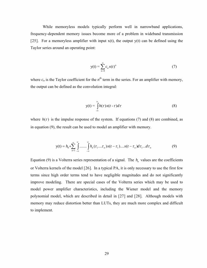
While memoryless models typically perform well in narrowband applications,
frequency-dependent memory issues become more of a problem in wideband transmission
[25]. For a memoryless amplifier with input x(t), the output y(t) can be defined using the
Taylor series around an operating point:
(7) 0
y(t) = ( )nn
n
c x t∞
=∑
where cn is the Taylor coefficient for the nth term in the series. For an amplifier with memory,
the output can be defined as the convolution integral:
-
y(t) = ( ) ( - )h x t dτ τ τ∞
∞∫ (8)
where ( )h τ is the impulse response of the system. If equations (7) and (8) are combined, as
in equation (9), the result can be used to model an amplifier with memory.
0 1 11
y(t) ....... ( .... ) ( ).... ( ) ...n n nn
h h x t x t d d1 nτ τ τ τ τ∞ ∞∞
= −∞ −∞
= + − −∑ ∫ ∫ τ (9)
Equation (9) is a Volterra series representation of a signal. The values are the coefficients
or Volterra kernels of the model [
nh
26]. In a typical PA, it is only necessary to use the first few
terms since high order terms tend to have negligible magnitudes and do not significantly
improve modeling. There are special cases of the Volterra series which may be used to
model power amplifier characteristics, including the Wiener model and the memory
polynomial model, which are described in detail in [27] and [28]. Although models with
memory may reduce distortion better than LUTs, they are much more complex and difficult
to implement.
29

2.4.5 Non-adaptive Predistortion Algorithm
Some functionality of the predistorter algorithm used in this project has already been
developed in MATLAB by a previous MQP [29]. The MATLAB code for the predistorter
written prior to this project is included in Appendix B.
The previously developed predistorter used static values for the PA transfer function,
defined using the Saleh model [30]. Using the model, equation (10) defines the input to the
PA.
0x(t) ( ) cos[ ( )]r t t tω ψ= + (10)
where r(t) and ψ(t) are the normalized amplitude and the phase of the input signal,
respectively. Equation (11) was used to define the magnitude of the PA output A[r(t)] in
response to the normalized input magnitude, or the AM-AM characteristics.
2
( )[ ( )]
1 ( )a
a
r tA r t
r tαβ
=+
(11)
Equation (12) was used to define the PA output phase Φ[r(t)] in response to the
normalized input magnitude, or the AM-PM characteristics.
2
2
( )[ ( )]
1 ( )r t
r tr t
φ
φ
αβ
Φ =+
(12)
In equations (11) and (12), aα , aβ , φα , and φβ are the coefficients which produced
the best fit model of the measured amplifier characteristics. The overall output of the PA,
y(t), was then defined by equation (13).
0y(t) [ ( )]cos ( ) [ ( )]A r t t t r tω ψ= + + Φ (13)
Equations (8) and (9) were used to create arrays of values for the PA characteristics.
The digital input was randomly generated in MATLAB. The predistorter found the ideal
output for any given input by multiplying the input by a constant which defines the linear
gain in the model. Once the ideal output was determined, the AM-AM and AM-PM arrays
30
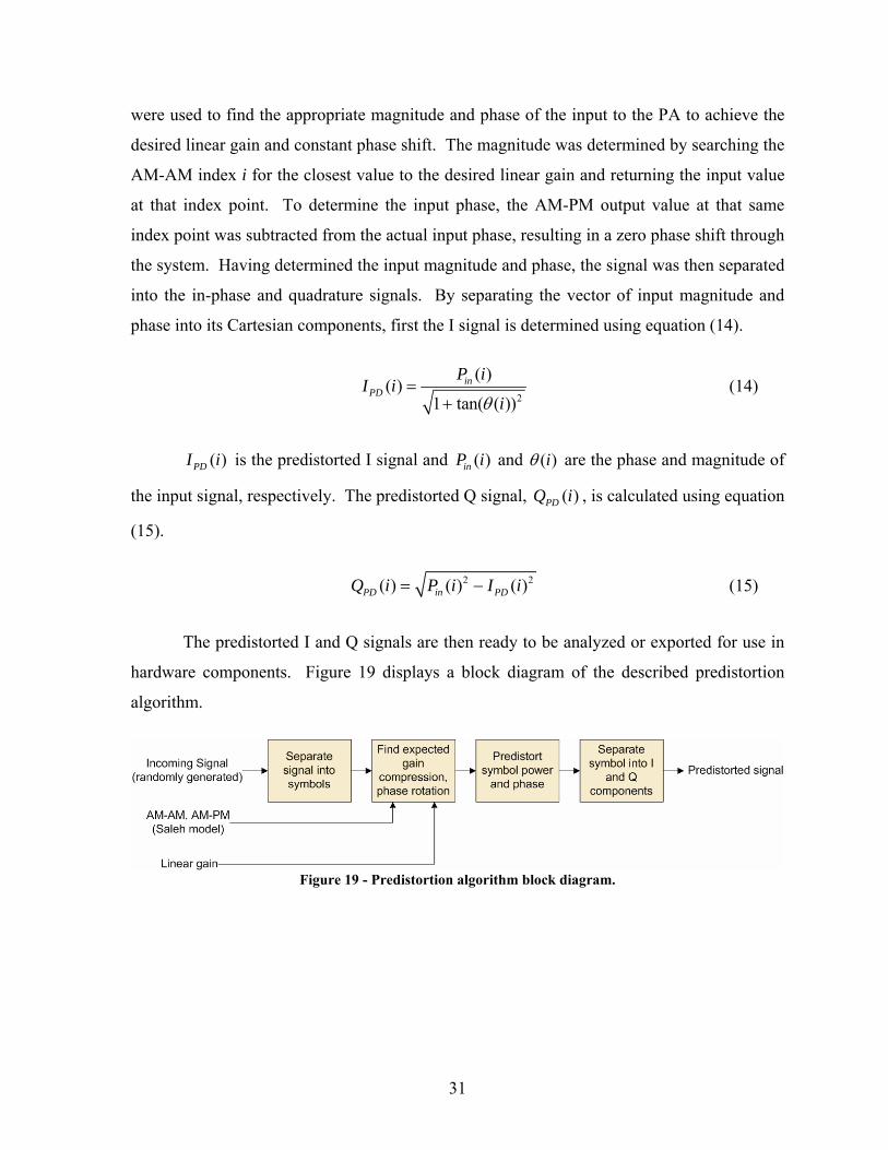
were used to find the appropriate magnitude and phase of the input to the PA to achieve the
desired linear gain and constant phase shift. The magnitude was determined by searching the
AM-AM index i for the closest value to the desired linear gain and returning the input value
at that index point. To determine the input phase, the AM-PM output value at that same
index point was subtracted from the actual input phase, resulting in a zero phase shift through
the system. Having determined the input magnitude and phase, the signal was then separated
into the in-phase and quadrature signals. By separating the vector of input magnitude and
phase into its Cartesian components, first the I signal is determined using equation (14).
2
( )( )
1 tan( ( ))in
PDP i
I iiθ
=+
(14)
( )PDI i is the predistorted I signal and and ( )inP i ( )iθ are the phase and magnitude of
the input signal, respectively. The predistorted Q signal, , is calculated using equation ( )PDQ i
(15).
2( ) ( ) ( )PD in PDQ i P i I i= − 2 (15)
The predistorted I and Q signals are then ready to be analyzed or exported for use in
hardware components. Figure 19 displays a block diagram of the described predistortion
algorithm.
Figure 19 - Predistortion algorithm block diagram.
31

3 Software: Predistorter and Pattern Generator The software-based design of the system consists of MATLAB code to generate a
lookup table (LUT) of predistorted symbols and VHDL code to cycle through the symbols
and output them from a field-programmable gate array (FPGA).
3.1 MATLAB Predistorter
The purpose of the MATLAB code is to generate LUTs for the predistortion of the in-
phase and quadrature (I and Q) signals. Figure 20 shows the block diagram for the
MATLAB predistorter used in this project.
Figure 20 - MATLAB predistorter block diagram.
Our MATLAB predistorter allows the user to enter S-parameter measurements from a
network analyzer or values exported from an Advanced Design System (ADS) model of the
PA, instead of relying on the Saleh model. The algorithm uses the PA measurements to
calculate the expected gain compression and phase rotation for each symbol, with n possible
values for n-QAM. Each symbol is then predistorted by compensating for the expected
nonlinearities as described in Section 2.4.5. Each predistorted symbol is separated into 16-bit
I and 16-bit Q components which are stored in arrays. The arrays of predistorted I and Q
values are written to text files to be used as LUTs in VHDL. Appendix A includes the
MATLAB code written or updated for this project.
32
3.2 FPGA Pattern Generator
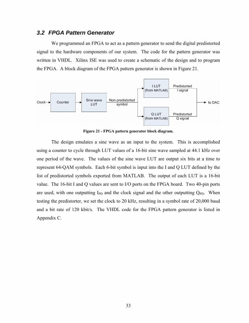
We programmed an FPGA to act as a pattern generator to send the digital predistorted
signal to the hardware components of our system. The code for the pattern generator was
written in VHDL. Xilinx ISE was used to create a schematic of the design and to program
the FPGA. A block diagram of the FPGA pattern generator is shown in Figure 21.
Figure 21 - FPGA pattern generator block diagram.
The design emulates a sine wave as an input to the system. This is accomplished
using a counter to cycle through LUT values of a 16-bit sine wave sampled at 44.1 kHz over
one period of the wave. The values of the sine wave LUT are output six bits at a time to
represent 64-QAM symbols. Each 6-bit symbol is input into the I and Q LUT defined by the
list of predistorted symbols exported from MATLAB. The output of each LUT is a 16-bit
value. The 16-bit I and Q values are sent to I/O ports on the FPGA board. Two 40-pin ports
are used, with one outputting IPD and the clock signal and the other outputting QPD. When
testing the predistorter, we set the clock to 20 kHz, resulting in a symbol rate of 20,000 baud
and a bit rate of 120 kbit/s. The VHDL code for the FPGA pattern generator is listed in
Appendix C.
33
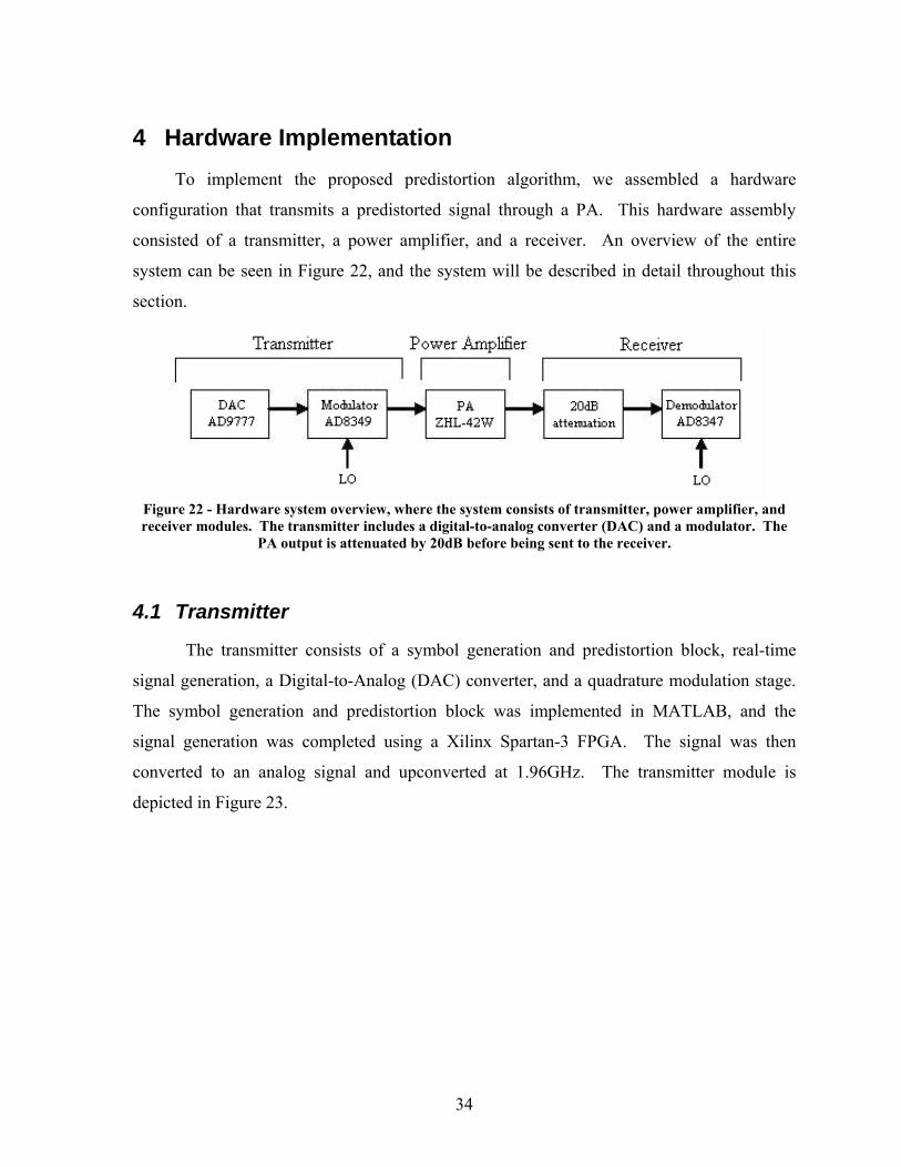
4 Hardware Implementation To implement the proposed predistortion algorithm, we assembled a hardware
configuration that transmits a predistorted signal through a PA. This hardware assembly
consisted of a transmitter, a power amplifier, and a receiver. An overview of the entire
system can be seen in Figure 22, and the system will be described in detail throughout this
section.
Figure 22 - Hardware system overview, where the system consists of transmitter, power amplifier, and receiver modules. The transmitter includes a digital-to-analog converter (DAC) and a modulator. The
PA output is attenuated by 20dB before being sent to the receiver.
4.1 Transmitter
The transmitter consists of a symbol generation and predistortion block, real-time
signal generation, a Digital-to-Analog (DAC) converter, and a quadrature modulation stage.
The symbol generation and predistortion block was implemented in MATLAB, and the
signal generation was completed using a Xilinx Spartan-3 FPGA. The signal was then
converted to an analog signal and upconverted at 1.96GHz. The transmitter module is
depicted in Figure 23.
34
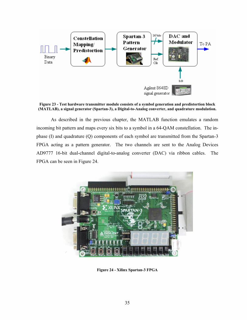
Figure 23 - Test hardware transmitter module consists of a symbol generation and predistortion block
(MATLAB), a signal generator (Spartan-3), a Digital-to-Analog converter, and quadrature modulation.
As described in the previous chapter, the MATLAB function emulates a random
incoming bit pattern and maps every six bits to a symbol in a 64-QAM constellation. The in-
phase (I) and quadrature (Q) components of each symbol are transmitted from the Spartan-3
FPGA acting as a pattern generator. The two channels are sent to the Analog Devices
AD9777 16-bit dual-channel digital-to-analog converter (DAC) via ribbon cables. The
FPGA can be seen in Figure 24.
Figure 24 - Xilinx Spartan-3 FPGA
35
The input to the AD9777 DAC from the FPGA is through two 16 bit ports, and the
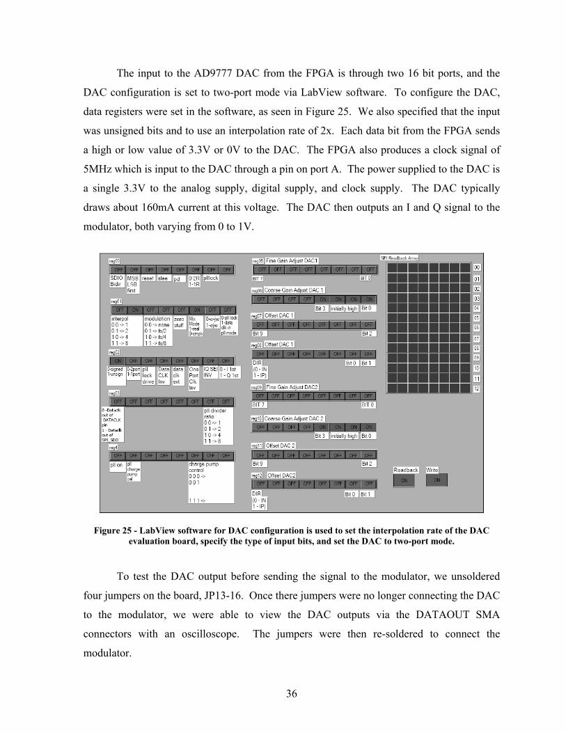
DAC configuration is set to two-port mode via LabView software. To configure the DAC,
data registers were set in the software, as seen in Figure 25. We also specified that the input
was unsigned bits and to use an interpolation rate of 2x. Each data bit from the FPGA sends
a high or low value of 3.3V or 0V to the DAC. The FPGA also produces a clock signal of
5MHz which is input to the DAC through a pin on port A. The power supplied to the DAC is
a single 3.3V to the analog supply, digital supply, and clock supply. The DAC typically
draws about 160mA current at this voltage. The DAC then outputs an I and Q signal to the
modulator, both varying from 0 to 1V.
Figure 25 - LabView software for DAC configuration is used to set the interpolation rate of the DAC evaluation board, specify the type of input bits, and set the DAC to two-port mode.
To test the DAC output before sending the signal to the modulator, we unsoldered
four jumpers on the board, JP13-16. Once there jumpers were no longer connecting the DAC
to the modulator, we were able to view the DAC outputs via the DATAOUT SMA
connectors with an oscilloscope. The jumpers were then re-soldered to connect the
modulator.
36
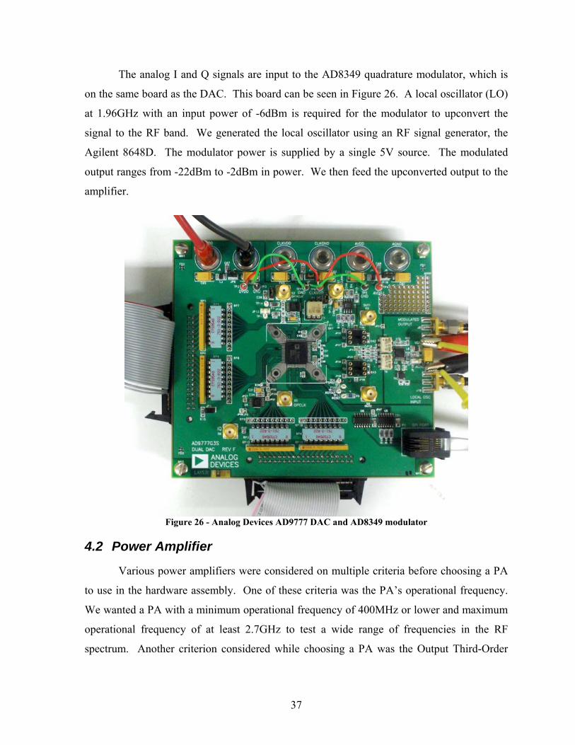
The analog I and Q signals are input to the AD8349 quadrature modulator, which is
on the same board as the DAC. This board can be seen in Figure 26. A local oscillator (LO)
at 1.96GHz with an input power of -6dBm is required for the modulator to upconvert the
signal to the RF band. We generated the local oscillator using an RF signal generator, the
Agilent 8648D. The modulator power is supplied by a single 5V source. The modulated
output ranges from -22dBm to -2dBm in power. We then feed the upconverted output to the
amplifier.
Figure 26 - Analog Devices AD9777 DAC and AD8349 modulator
4.2 Power Amplifier
Various power amplifiers were considered on multiple criteria before choosing a PA
to use in the hardware assembly. One of these criteria was the PA’s operational frequency.
We wanted a PA with a minimum operational frequency of 400MHz or lower and maximum
operational frequency of at least 2.7GHz to test a wide range of frequencies in the RF
spectrum. Another criterion considered while choosing a PA was the Output Third-Order
37
Intercept Point (OIP3). We also considered the output power of the amplifier; if the output
power is very low, we may not be able to see the results of our predistorter.
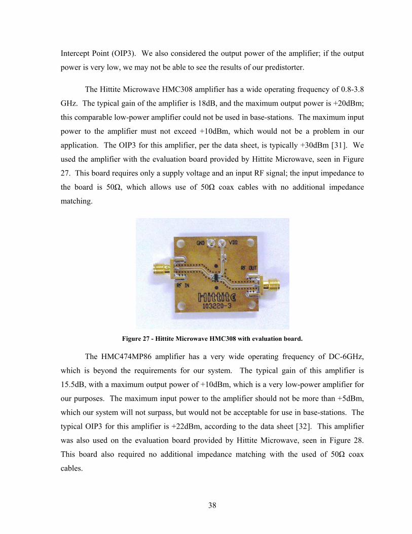
The Hittite Microwave HMC308 amplifier has a wide operating frequency of 0.8-3.8
GHz. The typical gain of the amplifier is 18dB, and the maximum output power is +20dBm;
this comparable low-power amplifier could not be used in base-stations. The maximum input
power to the amplifier must not exceed +10dBm, which would not be a problem in our
application. The OIP3 for this amplifier, per the data sheet, is typically +30dBm [31]. We
used the amplifier with the evaluation board provided by Hittite Microwave, seen in Figure
27. This board requires only a supply voltage and an input RF signal; the input impedance to
the board is 50Ω, which allows use of 50Ω coax cables with no additional impedance
matching.
Figure 27 - Hittite Microwave HMC308 with evaluation board.
The HMC474MP86 amplifier has a very wide operating frequency of DC-6GHz,
which is beyond the requirements for our system. The typical gain of this amplifier is
15.5dB, with a maximum output power of +10dBm, which is a very low-power amplifier for
our purposes. The maximum input power to the amplifier should not be more than +5dBm,
which our system will not surpass, but would not be acceptable for use in base-stations. The
typical OIP3 for this amplifier is +22dBm, according to the data sheet [32]. This amplifier
was also used on the evaluation board provided by Hittite Microwave, seen in Figure 28.
This board also required no additional impedance matching with the used of 50Ω coax
cables.
38
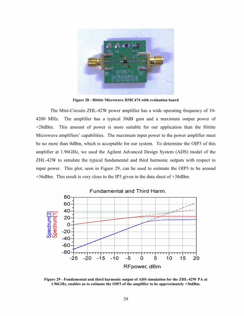
Figure 28 - Hittite Microwave HMC474 with evaluation board
The Mini-Circuits ZHL-42W power amplifier has a wide operating frequency of 10-
4200 MHz. The amplifier has a typical 30dB gain and a maximum output power of
+28dBm. This amount of power is more suitable for our application than the Hittite
Microwave amplifiers’ capabilities. The maximum input power to the power amplifier must
be no more than 0dBm, which is acceptable for our system. To determine the OIP3 of this
amplifier at 1.96GHz, we used the Agilent Advanced Design System (ADS) model of the
ZHL-42W to simulate the typical fundamental and third harmonic outputs with respect to
input power. This plot, seen in Figure 29, can be used to estimate the OIP3 to be around
+36dBm. This result is very close to the IP3 given in the data sheet of +38dBm.
Figure 29 - Fundamental and third harmonic output of ADS simulation for the ZHL-42W PA at 1.96GHz, enables us to estimate the OIP3 of the amplifier to be approximately +36dBm.
39

The ZHL-42W power amplifier requires a supply voltage of +15V. The maximum
input power to avoid damaging the PA is 0dBm. In our system, the maximum input power
was 0dBm, producing a maximum output power of +28dBm. This output needs to be
attenuated before being fed into the demodulator.
4.3 Receiver
The receiver consists of an attenuator and a quadrature demodulation stage, as
depicted in Figure 30.
Figure 30 - Test hardware receiver module consists of a 20dB attenuator and an AD8349 quadrature
demodulator.
The PA output needs to be attenuated before being sent to the demodulator, and we
used a 20dB attenuator for this purpose. The maximum input power recommended for the
AD8347 demodulator is +10dBm. Since the maximum output of our power amplifier during
our tests is +28dBm, we know that demodulator will not be damaged by the input if we
attenuate the input signal power by 20dB. The quadrature demodulator will be used to
retrieve the baseband representation of the analog I and Q signals. The Agilent 8648D signal
generator provides a Local Oscillator frequency of 1.96GHz to the demodulator, the same
signal used as a local oscillator for the modulation stage. A supply voltage of +5V is needed
to power the device, which is also the same source required by the AD8349 modulator. The
AD8347 board can be seen in Figure 31.
40
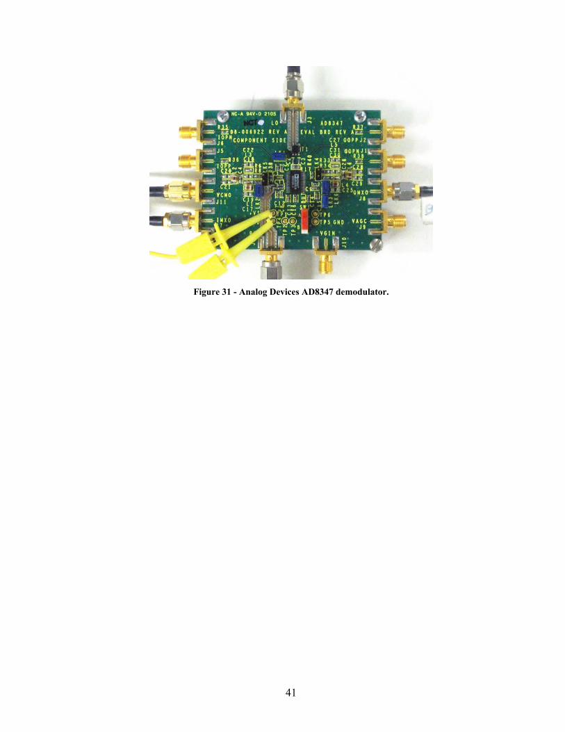
Figure 31 - Analog Devices AD8347 demodulator.
41
5 Results
In this section, we present our results of predistorter simulations and hardware tests.
First we present results of running dual tone test and predistorter simulations with an ADS
model of a power amplifier. We also produced simulation results using S-parameter
measurements to define the PA characteristics. Finally, we show the test results from using
the FPGA and other hardware components.
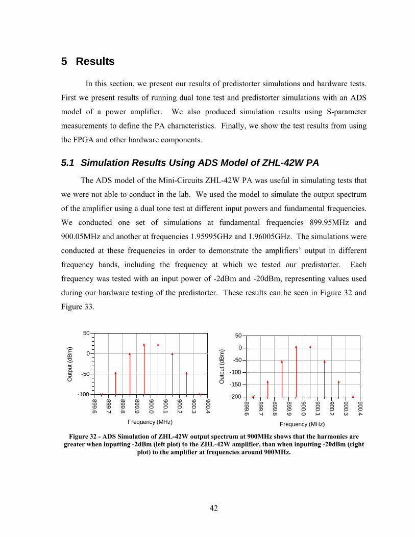
5.1 Simulation Results Using ADS Model of ZHL-42W PA
The ADS model of the Mini-Circuits ZHL-42W PA was useful in simulating tests that
we were not able to conduct in the lab. We used the model to simulate the output spectrum
of the amplifier using a dual tone test at different input powers and fundamental frequencies.
We conducted one set of simulations at fundamental frequencies 899.95MHz and
900.05MHz and another at frequencies 1.95995GHz and 1.96005GHz. The simulations were
conducted at these frequencies in order to demonstrate the amplifiers’ output in different
frequency bands, including the frequency at which we tested our predistorter. Each
frequency was tested with an input power of -2dBm and -20dBm, representing values used
during our hardware testing of the predistorter. These results can be seen in Figure 32 and
Figure 33.
899.7
899.8
899.9
900.0
900.1
900.2
900.3
899.6
900.4
-50
0
-100
50
Frequency (MHz)
Out
put (
dBm
)
899.7
899.8
899.9
900.0
900.1
900.2
900.3
899.6
900.4
-150
-100
-50
0
-200
50
Frequency (MHz)
Out
put (
dBm
)
Figure 32 - ADS Simulation of ZHL-42W output spectrum at 900MHz shows that the harmonics are
greater when inputting -2dBm (left plot) to the ZHL-42W amplifier, than when inputting -20dBm (right plot) to the amplifier at frequencies around 900MHz.
42
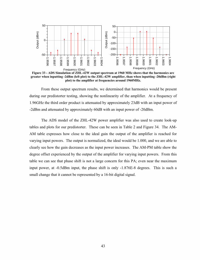
1.9597
1.9598
1.9599
1.9600
1.9601
1.9602
1.9603
1.9596
1.9604
0
-50
50
Frequency (GHz)
Out
put (
dBm
)
1.9597
1.9598
1.9599
1.9600
1.9601
1.9602
1.9603
1.9596
1.9604
-150
-100
-50
0
-200
50
Frequency (GHz)
Out
put (
dBm
)
Figure 33 - ADS Simulation of ZHL-42W output spectrum at 1960 MHz shows that the harmonics are
greater when inputting -2dBm (left plot) to the ZHL-42W amplifier, than when inputting -20dBm (right plot) to the amplifier at frequencies around 1960MHz.
From these output spectrum results, we determined that harmonics would be present
during our predistorter testing, showing the nonlinearity of the amplifier. At a frequency of
1.96GHz the third order product is attenuated by approximately 23dB with an input power of
-2dBm and attenuated by approximately 60dB with an input power of -20dBm.
The ADS model of the ZHL-42W power amplifier was also used to create look-up
tables and plots for our predistorter. These can be seen in Table 2 and Figure 34. The AM-
AM table expresses how close to the ideal gain the output of the amplifier is reached for
varying input powers. The output is normalized, the ideal would be 1.000, and we are able to
clearly see how the gain decreases as the input power increases. The AM-PM table show the
degree offset experienced by the output of the amplifier for varying input powers. From this
table we can see that phase shift is not a large concern for this PA; even near the maximum
input power, at -0.5dBm input, the phase shift is only -1.876E-8 degrees. This is such a
small change that it cannot be represented by a 16-bit digital signal.
43
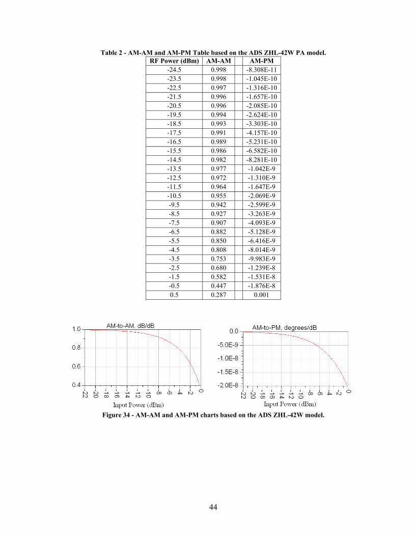
Table 2 - AM-AM and AM-PM Table based on the ADS ZHL-42W PA model. RF Power (dBm) AM-AM AM-PM
-24.5 0.998 -8.308E-11 -23.5 0.998 -1.045E-10 -22.5 0.997 -1.316E-10 -21.5 0.996 -1.657E-10 -20.5 0.996 -2.085E-10 -19.5 0.994 -2.624E-10 -18.5 0.993 -3.303E-10 -17.5 0.991 -4.157E-10 -16.5 0.989 -5.231E-10 -15.5 0.986 -6.582E-10 -14.5 0.982 -8.281E-10 -13.5 0.977 -1.042E-9 -12.5 0.972 -1.310E-9 -11.5 0.964 -1.647E-9 -10.5 0.955 -2.069E-9 -9.5 0.942 -2.599E-9 -8.5 0.927 -3.263E-9 -7.5 0.907 -4.093E-9 -6.5 0.882 -5.128E-9 -5.5 0.850 -6.416E-9 -4.5 0.808 -8.014E-9 -3.5 0.753 -9.983E-9 -2.5 0.680 -1.239E-8 -1.5 0.582 -1.531E-8 -0.5 0.447 -1.876E-8 0.5 0.287 0.001
Figure 34 - AM-AM and AM-PM charts based on the ADS ZHL-42W model.
44
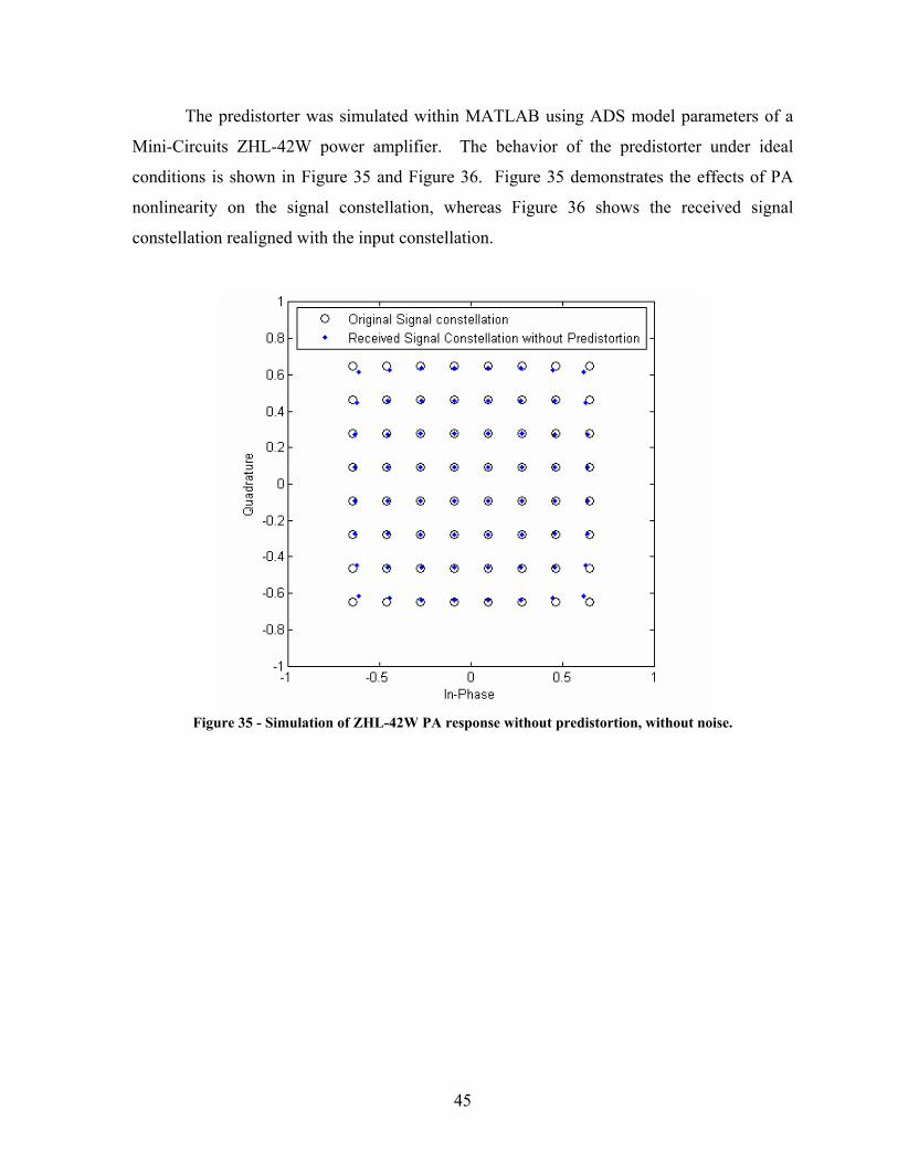
The predistorter was simulated within MATLAB using ADS model parameters of a
Mini-Circuits ZHL-42W power amplifier. The behavior of the predistorter under ideal
conditions is shown in Figure 35 and Figure 36. Figure 35 demonstrates the effects of PA
nonlinearity on the signal constellation, whereas Figure 36 shows the received signal
constellation realigned with the input constellation.
Figure 35 - Simulation of ZHL-42W PA response without predistortion, without noise.
45

Figure 36 - Simulation of ZHL-42W PA response with predistortion, without noise.
The algorithm successfully predistorted the signal up to the saturation point of the PA
characteristic. Since the simulation was run using ideal conditions, the error vector
magnitude (EVM) of the received constellation with predistortion was zero. The EVM was
typically 0.013 when the simulation was run without predistorting the signal.
The simulation was run once again with simulated noise added to the system. The
energy-per-bit (Eb) per noise power spectral (N0) density was 35dB. With noise simulation,
the EVM of the received signal is typically 0.005 with the predistorter and 0.017 without the
predistorter. This demonstrates that the predistorter is able to reduce the EVM by about a
factor of three even when transmitting a noisy signal. The received signals are shown with
and without predistortion, in Figure 37 and Figure 38, respectively.
46
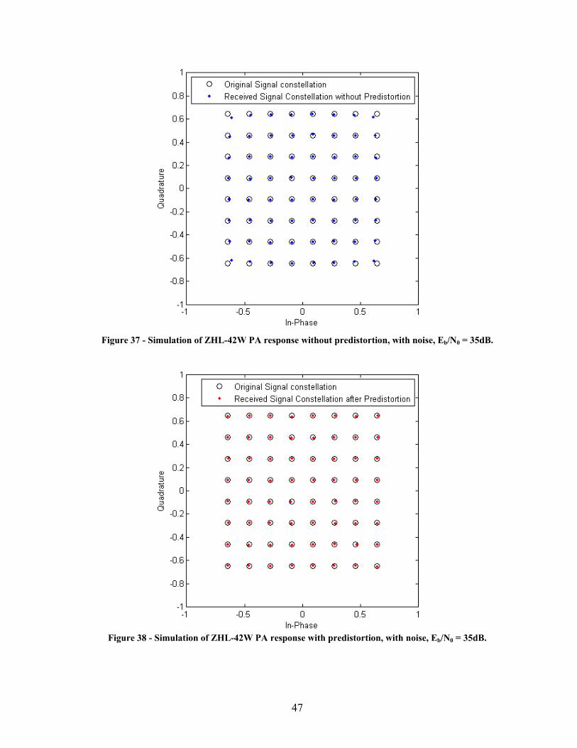
Figure 37 - Simulation of ZHL-42W PA response without predistortion, with noise, Eb/N0 = 35dB.
Figure 38 - Simulation of ZHL-42W PA response with predistortion, with noise, Eb/N0 = 35dB.
47
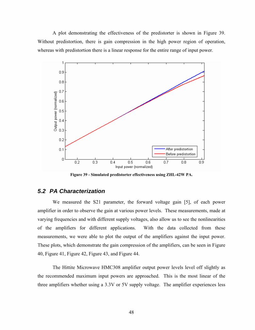
A plot demonstrating the effectiveness of the predistorter is shown in Figure 39.
Without predistortion, there is gain compression in the high power region of operation,
whereas with predistortion there is a linear response for the entire range of input power.
Figure 39 - Simulated predistorter effectiveness using ZHL-42W PA.
5.2 PA Characterization
We measured the S21 parameter, the forward voltage gain [5], of each power
amplifier in order to observe the gain at various power levels. These measurements, made at
varying frequencies and with different supply voltages, also allow us to see the nonlinearities
of the amplifiers for different applications. With the data collected from these
measurements, we were able to plot the output of the amplifiers against the input power.
These plots, which demonstrate the gain compression of the amplifiers, can be seen in Figure
40, Figure 41, Figure 42, Figure 43, and Figure 44.
The Hittite Microwave HMC308 amplifier output power levels level off slightly as
the recommended maximum input powers are approached. This is the most linear of the
three amplifiers whether using a 3.3V or 5V supply voltage. The amplifier experiences less
48

gain compression when using a 3.3V supply. When using a 5V supply voltage, the amplifier
experiences the most gain compression with an input frequency of 2.4GHz.
The other Hittite Microwave amplifier, the HMC474, is less linear than the previous.
This amplifier operates better when using a 5V supply voltage rather than a 3.3V supply.
The amplifier experiences the most gain compression with an input frequency of 2.4GHz.
The Mini-Circuits ZHL-42W amplifier was tested using only a 15V power supply, as
this is the only recommended source per the data sheet. This PA’s gain compression is much
more obvious than the two Hittite Microwave PAs, as can be seen in the output-input power
plots. Based on these figures, we can determine that our predistortion technique will be most
effective using the ZHL-42W.
Figure 40 - Gain compression of HMC308 amplifier with a 3.3V supply is not dramatic when a supply
voltage of 3.3V is used.
49

Figure 41 - Gain compression of HMC308 amplifier with a 5V supply is most obvious with an input
frequency of 2.4GHz.
Figure 42 - Gain compression of HMC474 amplifier with a 3.3V supply is noticeable at all frequencies
tested except at 6.0GHz.
50

Figure 43 - Gain compression of HMC474 amplifier with a 5V supply is most obvious with an input
frequency of 2.4GHz.
Figure 44 - Gain compression of ZHL-42W amplifier is noticeable at all frequencies tested with the
exception of 900MHz.
51

From the S21 parameter measurements used to demonstrate the gain compression of
the amplifiers, we calculated the 1-dB compression point for the ZHL-42W PA. The Hittite
amplifiers’ gain did not decrease by 1 dB or more with our measurements at any input
frequency and an input power up to 0dBm, the maximum for our hardware testing. The
ZHL-42W amplifier’s gain also did not decrease by 1dB when an input frequency of
900MHz was used. The 1-dB compression point of the ZHL-42W PA occurred when the
input power reached -3.5dBm when inputting a signal at 1.96GHz, when the input power
reached -4.8dBm when inputting a signal at 2.4GHz, and when the input power reached
-6.4dBm when inputting a signal at 4.2GHz.
Using the obtained 1-dB compression points, we were also able to approximate the
OIP3 of the ZHL-42W when operating at the tested frequencies by adding 9.66dB, per (4).
The OIP3 at 1.96GHz is +6.16dB, at 2.4GHz is +4.86dB, and at 4.2GHz is +3.26dB.
5.3 Simulation Results Using S-parameter Measurements
Using the S21 forward voltage gain measurements we made for each amplifier, we
were able to create simulations of expected results for our predistortion system. These
simulations neglected the effect of phase shift, which we believed to be acceptable due to the
negligible amount of measured phase shift during our amplifier characterization and ADS
simulations. The simulations demonstrated that the ZHL-42W power amplifier performed
worse without the predistorter than the HMC308 or HMC474 amplifiers, which we expected
based on the gain compression charts for the three PAs. The simulation results for the ZHL-
42W can be found in Figure 45, Figure 46, and Figure 47. These results provide greater
precision, since the simulations were created using actual measurements for this particular
ZHL-42W amplifier, rather than a generalized model.
52

Figure 45 - ZHL-42W received signal without predistortion shows gain compression at the outermost
symbols.
Figure 46 - ZHL-42W received signal after predistortion showing the corrected output.
53
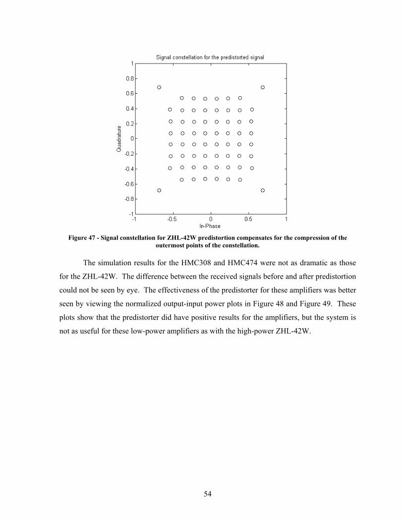
Figure 47 - Signal constellation for ZHL-42W predistortion compensates for the compression of the
outermost points of the constellation.
The simulation results for the HMC308 and HMC474 were not as dramatic as those
for the ZHL-42W. The difference between the received signals before and after predistortion
could not be seen by eye. The effectiveness of the predistorter for these amplifiers was better
seen by viewing the normalized output-input power plots in Figure 48 and Figure 49. These
plots show that the predistorter did have positive results for the amplifiers, but the system is
not as useful for these low-power amplifiers as with the high-power ZHL-42W.
54

Figure 48 - Predistortion effectiveness plot for HMC308 shows that the predistorted received signal does
not experience the gain compression that the non-predistorted received signal does. The input and output power are viewed only from 50-100% of the maximum power.
Figure 49 - Predistortion effectiveness plot for HMC474 shows that the predistorter does reduce gain compression in the received signal. The input and output power are viewed only from 80-100% of the maximum power. The effectiveness is small, with a difference not seen until the input power reaches
about 90% of its maximum.
55
5.4 Hardware Results
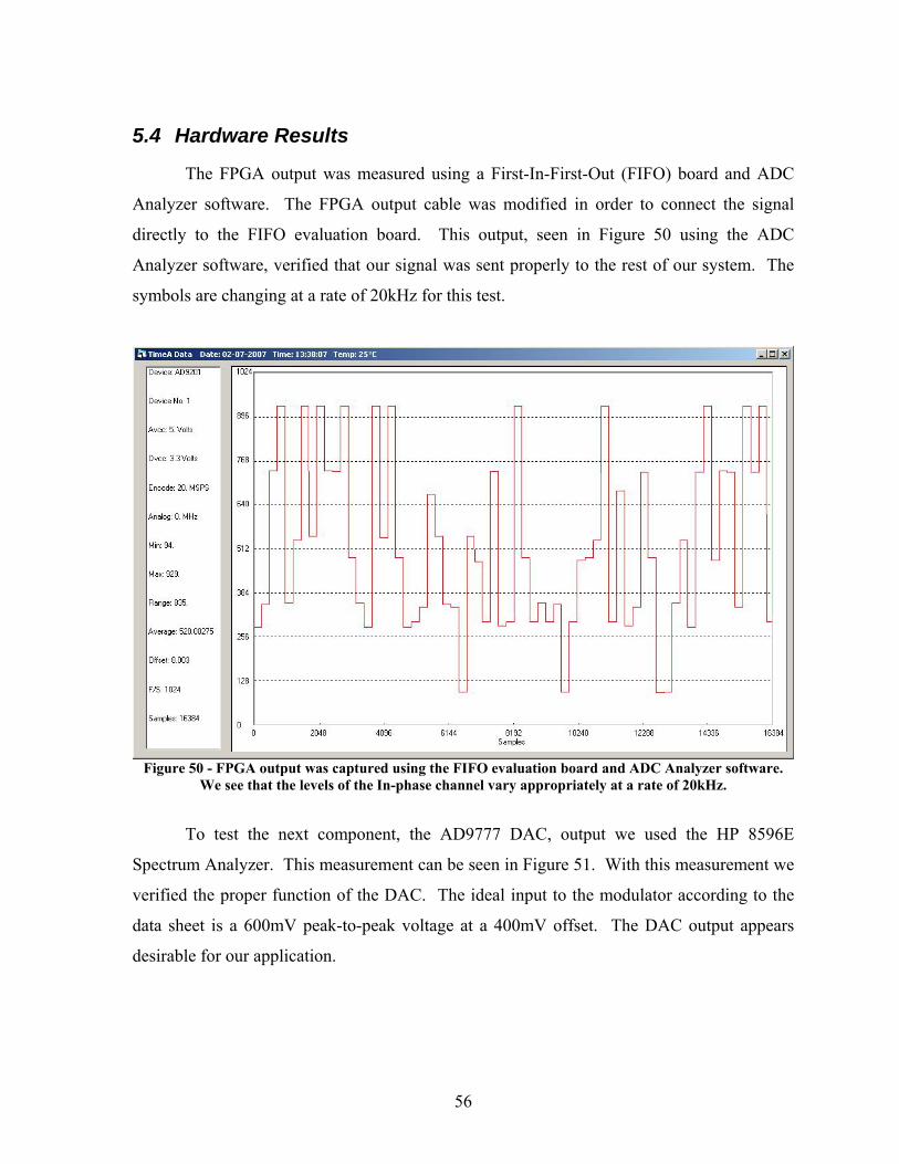
The FPGA output was measured using a First-In-First-Out (FIFO) board and ADC
Analyzer software. The FPGA output cable was modified in order to connect the signal
directly to the FIFO evaluation board. This output, seen in Figure 50 using the ADC
Analyzer software, verified that our signal was sent properly to the rest of our system. The
symbols are changing at a rate of 20kHz for this test.
Figure 50 - FPGA output was captured using the FIFO evaluation board and ADC Analyzer software.
We see that the levels of the In-phase channel vary appropriately at a rate of 20kHz.
To test the next component, the AD9777 DAC, output we used the HP 8596E
Spectrum Analyzer. This measurement can be seen in Figure 51. With this measurement we
verified the proper function of the DAC. The ideal input to the modulator according to the
data sheet is a 600mV peak-to-peak voltage at a 400mV offset. The DAC output appears
desirable for our application.
56

Figure 51 - DAC output viewed at 500kS/s
To test the modulator output, we used the HP 8596E Spectrum Analyzer again. This
measurement made at a high sampling rate of 50 MS/s can be seen in Figure 52 to
demonstrate that the amplitude is actually being modulated. With this measurement, we
were able to verify that the changing symbols were being sent to the PA appropriately. The
symbol rate for this test was 20kHz, and the RF carrier signal was 1.96GHz.
57
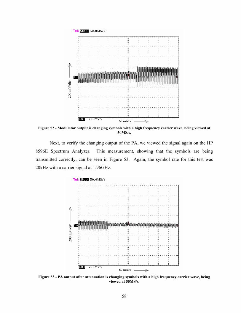
Figure 52 - Modulator output is changing symbols with a high frequency carrier wave, being viewed at
50MS/s.
Next, to verify the changing output of the PA, we viewed the signal again on the HP
8596E Spectrum Analyzer. This measurement, showing that the symbols are being
transmitted correctly, can be seen in Figure 53. Again, the symbol rate for this test was
20kHz with a carrier signal at 1.96GHz.
Figure 53 - PA output after attenuation is changing symbols with a high frequency carrier wave, being
viewed at 50MS/s.
58

Finally, we tested the output of the demodulator, the receiver of our system. The I
and Q signals were viewed separately with the HP 8596E Spectrum Analyzer. The baseband
signals seen in Figure 54 and Figure 55, with peak-to-peak voltages of about 600mV, are the
signals output from the demodulator. These signals are changing at a rate of 20kHz.
Unfortunately, due to the sensitivity of RF transmission, the demodulator output was
inconsistent. Therefore, the system output could not be conclusively verified in the hardware
set-up we were able to complete using coax transmission lines. The system induced too
much noise to achieve the level of precision we would have required to confirm the
effectiveness of our predistortion hardware set-up.
Figure 54 – Voltage versus time IMXO output of demodulator showing the baseband linearized I signal.
The signals is changing at a rate of 20kHz and being sampled at a rate of 1MS/s.
59

Figure 55 – Voltage versus time QMXO output of demodulator showing the baseband linearized Q
signal. The signals is changing at a rate of 20kHz and being sampled at a rate of 1MS/s.
60

Conclusions and Recommendations This report presented our investigation of RFPA characteristics and predistortion
methods for linearization. We focused our efforts on characterizing the nonlinearities of
available PAs in order to implement a method of correcting gain compression and phase
rotation which occur in the high power region of PA operation. Predistortion of the digital
baseband signal was our chosen method because of its adaptability to varying PA
characteristics.
A predistortion algorithm developed in MATLAB by a previous MQP served as the
foundation of our project. That algorithm relies on a general nonlinear PA transfer function
defined by the Saleh model [30]. Our modified algorithm employs data from Advanced
Design System models or S-parameter measurements. After running the predistortion
algorithm, the predistorter writes the value of each predistorted symbol to a text file. This
text file is imported into a lookup table (LUT) written in VHDL. The rest of the VHDL
system is designed to cycle through the values of the LUT and output the predistorted symbol
associated with each value. The VHDL system is programmed to an FPGA for hardware
testing.
Once the VHDL design for the predistorter was implemented on the FPGA, its
operation is verified using a logic analyzer. The output was also captured onto a PC using an
Analog Devices’ First-In First-Out (FIFO) evaluation kit. Furthermore, Analog Devices’
ADC Analyzer software captures the output from the FIFO board onto the PC. The output
coming from the digital-to-analog converter (DAC), modulator, and power amplifier appear
as expected when viewed on the Tektronix TDS-784C oscilloscope.
The output of our demodulator, though changing symbols as desired, does not
produce consistent results. The noise in the system and the sensitivity involved with RF
signal transmission are too large to achieve the level of precision necessary to conclusively
verify the effectiveness of our predistortion hardware set-up.
If the predistorter is to be used to compensate for temperature and other short-term
effects, it must be used in a closed-loop configuration. The preferable method for
61

implementing a digital adaptive predistorter is using a digital signal processor (DSP).
However, the design of a truly adaptive predistorter, which takes into account memory
effects and other non-linear characteristics, may be beyond the time frame of an
undergraduate level project.
We have shown that our predistorter is capable of adapting to specific PA
characteristics each time the MATLAB function is executed with updated PA measurements.
This allows for correction of the nonlinearities of a specific PA rather than a general model,
as well as correction of long-term effects such as aging. The predistorter was simulated
within MATLAB and found to completely eliminate nonlinearities in the output signal up to
the saturation point of the PA. This resulted in an error vector magnitude of zero, even
without any back off of the input signal. We showed the performance of the predistorter
under non-ideal conditions by simulating noise. We also presented simulated results of the
predistorter performance with multiple models of PAs, and we found that our predistorter
was equally effective at linearizing each PA model.
62

Acknowledgements We thank the following people who helped us with this Major Qualifying Project:
• Professor Reinhold Ludwig (WPI)
• Professor John McNeill (WPI)
• David Buchanan (Analog Devices)
• Carlos Calvo (Analog Devices)
• Larry Hawkins (Analog Devices)
• Steve Reine (Analog Devices)
63

Appendix A: MATLAB Code I) Evaluate predistorter performance
<filename: test_predistorter_txt.m> % Author: Rahul Gupta and Saad Ahmad % Modified: Christopher Serrano % % Predistorter test script % % Calls hpa_sweep to characterize PA, % Calls predistorter_v2 to run predistortion algorithm, % Calls hpa_v2 to distort signal according to PA characteristics, % Calculates EVM of the received signals % Generates plots demonstrating predistorter effectiveness, % predistorted input constellation, distorted output, % and linearized output, % Generates lookup table values for the predistorted input constellation clear all; clc; close all; %% Define constellation parameters M = 64; % Size of signal constellation k = log2(M); % Number of bits per symbol nsamp = 1; % Oversampling rate %% Modulation % Modulate using M-QAM. xsym = 0:M-1; y = qammod(xsym,M); %% Perform Power Sweep and Record the AMAM and AMPM characteristics r = 0:1e-4:1; % normalized range of power sweep o_power = hpa_sweep(r); AMAM = abs(o_power); AMPM = angle(o_power); %% Calculate linear gain using first 20% of AMAM values lin_max=round(length(AMAM)*0.20); lin_gain = mean(diff(AMAM(1:lin_max)))*length(AMAM); %% Set backoff percentage from saturation backoff_percent = 0; saturation = 1/lin_gain; % defines saturation point backoff = (100 - backoff_percent)/100*saturation; y = backoff*y ./ (max(abs(y))); % normalization %% Invoke the predistorter y_pd = predistorter_v2(y, y, r, AMAM, AMPM, lin_gain);
64
% Distorted output (without predistortion) ydist = hpa_v2(y, AMAM, AMPM); ydist = ydist/lin_gain; % Scale down to match original signal % Linearized output (after predistortion) ytx = hpa_v2(y_pd, AMAM, AMPM); ytx = ytx/lin_gain; % Scale down to match original signal %% Plot AM-AM after predistortion figure; %subplot(2,1,1); plot(sort(abs(y)), sort(abs(ytx)), 'b', 'LineWidth', 3); hold on; plot(sort(abs(y)), sort(abs(ydist)), 'r', 'LineWidth', 3); xlabel('Input power (normalized)'); ylabel('Output power (normalized)'); legend('After predistortion', 'Before predistortion'); title('Predistortion effectiveness analysis'); axis([min(abs(y)) max(abs(y)) 0 1]); hold off; % Plot AM-PM after predistortion subplot(2,1,2); title('AM-PM performance after predistortion'); plot(sort(abs(y)), sort(angle(ytx) - angle(y)), 'r--', 'LineWidth', 4); xlabel('Input Amplitude r'); ylabel('AMPM(r)'); axis([min(abs(y)) max(abs(y)) -0.2 0.2]); %% Noise simulation EbNo = 35; % In dB snr = EbNo + 10*log10(k) - 10*log10(nsamp); ytx_noise = awgn(ytx,snr,'measured'); ydist_noise = awgn(ydist,snr,'measured'); % Include the following two lines to generate plots without noise: %ytx_noise=ytx; %ydist_noise=ydist; %% Error Vector Magnitude % EVM with and without predistortion, with noise evm_pd = evm(y,ytx_noise); evm_nopd = evm(y,ydist_noise); %% Scatter Plots % Create scatter plot of input signal and distorted PA output % (with predistortion) on the same axes. h = scatterplot(y,nsamp,0,'ko'); hold on; scatterplot(ytx_noise,1,0,'r.',h); title('Simulation with predistortion'); legend('Original Signal constellation','Received Signal Constellation after Predistortion'); axis([-1 1 -1 1]); % Set axis ranges hold off; % Create scatter plot of input signal and distorted PA output
65
% (without predistortion) on the same axes. i = scatterplot(y,nsamp,0,'ko'); hold on; scatterplot(ydist_noise,1,0,'b.',i); legend('Original Signal constellation','Received Signal Constellation without Predistortion'); title('Simulation without predistortion'); axis([-1 1 -1 1]); % Set axis ranges hold off; % Observe the signal constellation for the predistorted input j = scatterplot(y_pd,1,0,'ko'); axis([-1 1 -1 1]); % Set axis ranges title('Signal constellation for the predistorted signal'); %% Export I and Q signals to text files export_iq(y_pd,'pd_out.txt ; ')export_iq(y,'iq_out.txt');
66

II) The predistorter function
<filename: predistorter_v2.m>
% Author: Saad Ahmad and Rahul Gupta % Modified: Christopher Serrano % Predistorter function % predistorter.m modified to run faster, % using LUT with N values for N-QAM function y_pd = predistorter_v2(y, y_lut, r, AMAM, AMPM, lin_gain) %% Using unique set of input symbols (y_lut), define predistorted LUT values (ypd_lut) for i=1:length(y_lut) expected_gain_of_y_lut(i) = lin_gain * abs(y_lut(i)); % Compute expected gain based upon the linear gain if(expected_gain_of_y_lut(i) > max(AMAM) ) expected_gain_of_y_lut(i) = max(AMAM); end % Backtrack to find the index that gives the AMAM closes to the % expected gain pd_index = find( abs(AMAM - expected_gain_of_y_lut(i)) < 1e-4); tmp = r(pd_index(1)); % Find the corresponding input. This will be the amplitude of the % predistorted input. pin(i) = tmp; % Theta is the arctan(Q_pd/I_pd) that is the angle of the vector represented by I_pd * j*Q_pd theta(i) = angle(y_lut(i)) - AMPM(pd_index(1)); I_pd(i) = (pin(i) ./ sqrt (1 + tan( theta(i) ).^2 ) ); % Solve for I_pd(i) and Q_pd(i) Q_pd(i) = sqrt(pin(i).^2 - I_pd(i).^2); % Make sign corrections if necessary theta_d(i) = theta(i) * 180 / pi; if ((theta_d(i) >= 0) && (theta_d(i) < 90) ) do nothing % end if ((theta_d(i) >= 90) && (theta_d(i) < 180) ) I_pd(i) = -abs(I_pd(i)); % Second quadrant I must be negative, while Q must be positive Q_pd(i) = abs(Q_pd(i)); end if ((theta_d(i) >= -180) && (theta_d(i) < -90) ) I_pd(i) = -abs(I_pd(i)); % Third quadrant: Both I and Q must be the same Q_pd(i) = -abs(Q_pd(i));
67

end if ((theta_d(i) >= -90) && (theta_d(i) < 0) ) I_pd(i) = abs(I_pd(i)); % Fourth quadrant I must be positive and Q must be negative Q_pd(i) = -abs(Q_pd(i)); end if ((theta_d(i) < -180) ) I_pd(i) = -abs(I_pd(i)); % Fourth quadrant I must be positive and Q must be negative Q_pd(i) = abs(Q_pd(i)); end if ((theta_d(i) < -180) && (theta_d(i) > 180) ) display('Error!! Error!! Error!! Error!!') end ypd_lut(i) = I_pd(i) - j*Q_pd(i); % Compute predistorted symbol ypd_lut(i) corresponding to y(i) end %% Perform predistortion using input signal (y) and LUT values (ypd_lut) y_pd = 0:0:length(y); % Preallocate space for y_pd to improve speed % LUT assignment loop for i=1:length(y) y_pd(i) = ypd_lut(y(i)==y_lut); end y_pd = y_pd'; % Transpose
68

III) Define power amplifier transfer function from measurements
<filename: hpa_sweep.m> % Author: Christopher Serrrano % % Read a text file with PA power and phase measurements, % generate AM-AM and AM-PM best fit values function output = hpa_v2(input_symbol); %% input_symbol(complex number) represents the mapped symbols on a constellation r = abs(input_symbol); % Magnitude theta = angle(input_symbol); % Phase %% Read in PA characteristics exported from ADS N=length(dlmread('Pin_Pout.txt'))-1; % number of samples -1 p_in = ((0:1:N)./N).'; % normalized Pin % Read in second column of Pin vs. Pout p_out=dlmread('Pin_Pout.txt','',[0,1,N,1]); % Read in second column of Pin vs. Phase phase_out=dlmread('Pin_Phase.txt','',[0,1,N,1]); % for ADS %% Normalization % Shift p_out values such that minimum value is zero p_out = p_out-min(p_out); % Scale such that maximum p_out value is one p_out = p_out/max(p_out); % Shift phase values such that first value is zero phase_out=phase_out-phase_out(1); %% Polynomial fitting degree=10; p_poly = polyfit(p_in,p_out,degree); phase_poly = polyfit(p_in,phase_out,degree); range = 0:1e-4:1; AMAM = polyval(p_poly,range); AMPM = polyval(phase_poly,range); %% Re-computing phase of the output theta = theta + AMPM; % Applying PA characteristic distortion to calculate the output output = AMAM.*cos(theta)+ j*AMAM.*sin(theta);
69
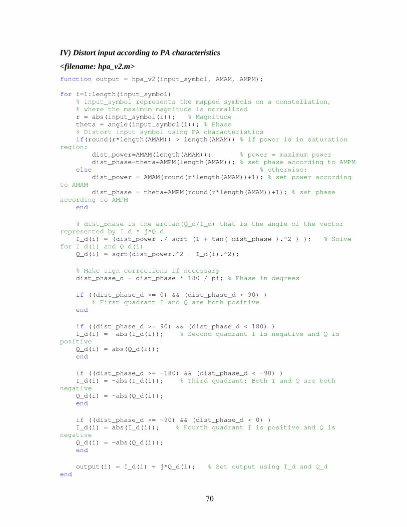
IV) Distort input according to PA characteristics
<filename: hpa_v2.m> function output = hpa_v2(input_symbol, AMAM, AMPM); for i=1:length(input_symbol) % input_symbol represents the mapped symbols on a constellation, % where the maximum magnitude is normalized r = abs(input_symbol(i)); % Magnitude theta = angle(input_symbol(i)); % Phase % Distort input symbol using PA characteristics if(round(r*length(AMAM)) > length(AMAM)) % if power is in saturation region: dist_power=AMAM(length(AMAM)); % power = maximum power dist_phase=theta+AMPM(length(AMAM)); % set phase according to AMPM else % otherwise: dist_power = AMAM(round(r*length(AMAM))+1); % set power according to AMAM dist_phase = theta+AMPM(round(r*length(AMAM))+1); % set phase according to AMPM end % dist_phase is the arctan(Q_d/I_d) that is the angle of the vector represented by I_d * j*Q_d I_d(i) = (dist_power ./ sqrt (1 + tan( dist_phase ).^2 ) ); % Solve for I_d(i) and Q_d(i) Q_d(i) = sqrt(dist_power.^2 - I_d(i).^2); % Make sign corrections if necessary dist_phase_d = dist_phase * 180 / pi; % Phase in degrees if ((dist_phase_d >= 0) && (dist_phase_d < 90) ) % First quadrant I and Q are both positive end if ((dist_phase_d >= 90) && (dist_phase_d < 180) ) I_d(i) = -abs(I_d(i)); % Second quadrant I is negative and Q is positive Q_d(i) = abs(Q_d(i)); end if ((dist_phase_d >= -180) && (dist_phase_d < -90) ) I_d(i) = -abs(I_d(i)); % Third quadrant: Both I and Q are both negative Q_d(i) = -abs(Q_d(i)); end if ((dist_phase_d >= -90) && (dist_phase_d < 0) ) I_d(i) = abs(I_d(i)); % Fourth quadrant I is positive and Q is negative Q_d(i) = -abs(Q_d(i)); end output(i) = I_d(i) + j*Q_d(i); % Set output using I_d and Q_d end
70

V) Calculate Error Vector Magnitude of the received signal
<filename: evm.m> % Author: Christopher Serrano % % Function to calculate error vector magnitude % Input tx and rx constellations with proper scaling: % tx = transmitted constellation % rx = received constellation % Output evm as floating point value function evm=evm(tx,rx) %% Separate into I and Q i_tx=real(tx); q_tx=imag(tx); i_rx=real(rx); q_rx=imag(rx); %% Perform EVM calculation % EVM formula evm = sqrt(mean((i_tx-i_rx).^2+(q_tx-q_rx).^2))/abs(max(tx)); % return EVM
71

Appendix B: MATLAB Code from Previous MQP I) Evaluate predistorter performance via constellation prewarping and dual-tone analysis
<filename: test_predistorter.m>
% Author: Rahul Gupta and Saad Ahmad % Program to assess % predistorter performance clear all; clc; close all; % Defining constellation parameters M = 64; % Size of signal constellation k = log2(M); % Number of bits per symbol n = 3e4; % Number of bits to process nsamp = 1; % Oversampling rate %%Signal Source % Emulates a real-world binary input x = randint(n,1); % Random binary data stream %% Bit-to-Symbol Mapping % Convert the bits in x into k-bit symbols. xsym = bi2de(reshape(x,k,length(x)/k).','left-msb'); %% Modulation % Modulate using M-QAM. y = qammod(xsym,M); backoff = 0.8; % Specify backoff percentage from saturation y = backoff*y ./ (max(abs(y))); % normalization %% Characterize the PA ytx = hpa(y); % see hpa.m %% Perform Power Sweep and Record the AMAM and AMPM characteristics r = 0:1e-4:1; o_power = hpa(r); AMAM = abs(o_power); AMPM = angle(o_power); % Linear gain setpoint (computed using the initial slope of the characteristic) lin_gain = 1.69461 ; % Invoke the predistorter y_pd = predistorter(y, r, AMAM, AMPM, lin_gain);
72

% Distorted output (without predistortion) ydist = hpa(y); % Linearized output (after predistortion) ytx = hpa(y_pd); %% Plot AM-AM after predistortion figure; subplot(2,1,1); plot(sort(abs(y)), sort(abs(hpa(y_pd))), 'r', 'LineWidth', 3); hold on; plot(sort(abs(y)), sort(abs(hpa(y))), 'b', 'LineWidth', 3); xlabel('Input Amplitude r'); ylabel('Output Amplitude AMAM(r)'); legend('After predistortion', 'Before predistortion'); title('Predistortion effectiveness analysis'); axis([min(abs(y)) max(abs(y)) 0 1]); hold off; %% Plot AM-PM after predistortion subplot(2,1,2); title('AM-PM performance after predistortion'); plot(sort(abs(y)), sort(angle(hpa(y_pd)) - angle(y)), 'r--', 'LineWidth', 4); xlabel('Input Amplitude r'); ylabel('AMPM(r)'); axis([min(abs(y)) max(abs(y)) -0.2 0.2]); %% Channel % Add noise EbNo = 35; % In dB snr = EbNo + 10*log10(k) - 10*log10(nsamp); ynoisy = awgn(ytx,snr,'measured'); ynoisy2 = awgn(ydist,snr,'measured'); %% Scatter Plot1 % Create scatter plot of input signal and distorted PA output % (without predistortion) on the same axes. h = scatterplot(y(1:nsamp*5e3),nsamp,0,'k*'); hold on; scatterplot(ynoisy(1:5e3),1,0,'m.',h); legend('Original Signal constellation','Received Signal Constellation after Predistortion'); axis([-1 1 -1 1]); % Set axis ranges hold off; %% Scatter Plot2 % Create scatter plot of input signal and distorted PA output % (WITh predistortion) on the same axes. i = scatterplot(y(1:nsamp*5e3),nsamp,0,'k*'); hold on; scatterplot(ynoisy2(1:5e3),1,0,'r.',i); legend('Original Signal constellation','Received Signal Constellation without Predistortion'); axis([-1 1 -1 1]); % Set axis ranges hold off; %% Scatter Plot3
73

% Observe the signal constellation for the predistorted input j = scatterplot(y_pd(1:5e3),1,0,'b*'); axis([-1 1 -1 1]); % Set axis ranges title('Signal constellation for the predistorted signal'); %% Pulse shape the data after converting it to 16-bit binary words % Take only single occurences for each unique symbol in y reps = 1; yuniq = zeros(M, reps); y = unique(y); for i=1:reps yuniq(:,i) = y; end yuniq = reshape(yuniq,1,reps*length(y)); IDATA = real(yuniq); QDATA = imag(yuniq); Interpoltype = 'gauss'; % Gaussian pulse shaping timestep = 1e-9; % 1ns - for computing the FFT symboltime = 1e-7; % 10MSym/sec Nbits = 16; % 16-bit quantization [totaltime, t,icomponent,qcomponent,interleaved] = pulseshape(interpoltype, timestep, IDATA, QDATA, symboltime, Nbits); %%% Prepare for multi-tone test %%% n = [0:1e4]; % Defining a four-tone signal closely centered around 0.25 f / Fs omega0 = 2*pi*(0.235); omega1 = 2*pi*(0.245); omega2 = 2*pi*(0.265); omega3 = 2*pi*(0.255); A0 = 0.175; A1 = 0.175; A2 = 0.175; A3 = 0.175; x1 = A0*cos(omega0*n) + A1*cos(omega1*n) + A2*cos(omega2*n)+ A3*cos(omega3*n); % Number of a FFT points. Must be of the form 2X where X is an integer N = 8192; % Computing FFT X_fft = (fft(x1,N)); X = fftshift(abs(X_fft)); % Shift zero-frequency component of discrete Fourier transform to center of spectrum Power = X.^2; % Power spectrum freq = [-N/2:N/2-1]/N; % Computing FFT of the PA output without PD yampout = hpa(x1); Y_fft = (fft(yampout,N)); Y = fftshift(abs(Y_fft)); Powery = Y.^2;
74

phasey = angle(Y_fft); dimen1 = length(freq)/2 + 1; dimen2 = length(freq); % Computing FFT of the PA output WITH PD x1_pd = predistorter(x1, r, AMAM, AMPM, lin_gain); y_ampout_withpd = hpa(x1_pd); Ypd_fft = (fft(y_ampout_withpd,N)); Ypd = fftshift(abs(Ypd_fft)); Powerypd = Ypd.^2; phaseypd = angle(Ypd_fft); %% Plot power spectral density to visualize improvement in IMD suppression (if any) % Input power spectral density figure; semilogy(freq(dimen1:dimen2),Power(dimen1:dimen2)./max(Power), 'r', 'LineWidth', 1.5); xlabel('Normalized Frequency (f / F_S)') ylabel('(dB)'); title ('Power Spectral Density of a four-tone input spectrum'); axis([0 0.5 10.^(-3.5) 10]); % Output power spectral density (without predistortion) figure; semilogy(freq(dimen1:dimen2),Powery(dimen1:dimen2)./max(Power), 'b', 'LineWidth',1.5); xlabel('Normalized Frequency (f / F_S)') ylabel('(dB)'); title ('Power Spectral Density of PA output illustrating Intermodulation Distortion '); axis([0 0.5 10.^(-3.5) 10.^2]); % Output power spectral density (with predistortion) figure; semilogy(freq(dimen1:dimen2),Powerypd(dimen1:dimen2)./max(Power), 'k', 'LineWidth',1.5); xlabel('Normalized Frequency (f / F_S)') ylabel('(dB)'); title ('Power Spectral Density of PA output illustrating Predistorter in action '); axis([0 0.5 10.^(-3.5) 10.^2]); %%% End of multi-tone routine%%%
II) The predistorter function
75

<filename: predistorter.m>
%% Author: Rahul Gupta %% Predistort the input signal one symbol at a time % Predistorter function requires the AMAM and AMPM curves function y_pd = predistor(y, r, AMAM, AMPM, lin_gain) for i=1:length(y) expected_gain_of_y(i) = lin_gain * abs(y(i)); % Compute expected gain based upon the linear gain if(expected_gain_of_y(i) > max(AMAM) ) expected_gain_of_y(i) = max(AMAM); end % Backtrack to find the index that gives the AMAM closes to the % expected gain pd_index = find( abs(AMAM - expected_gain_of_y(i)) < 1e-4); tmp = r(pd_index(1)); % Find the corresponding input. This will be the amplitude of
% the predistorted input. pin(i) = tmp; % Theta is the arctan(Q_pd/I_pd) that is the angle of the
% vector represented by I_pd * j*Q_pd
theta(i) = angle(y(i)) - AMPM(pd_index(1));
% Solve for I_pd(i) and Q_pd(i) I_pd(i) = (pin(i) ./ sqrt (1 + tan( theta(i) ).^2 ) ); Q_pd(i) = sqrt(pin(i).^2 - I_pd(i).^2); % Make sign corrections if necessary theta_d(i) = theta(i) * 180 / pi; if ((theta_d(i) >= 0) && (theta_d(i) < 90) ) % do nothing end if ((theta_d(i) >= 90) && (theta_d(i) < 180) ) I_pd(i) = -abs(I_pd(i));
% Second quadrant I must be negative, while Q must be positive Q_pd(i) = abs(Q_pd(i)); end if ((theta_d(i) >= -180) && (theta_d(i) < -90) ) I_pd(i) = -abs(I_pd(i));
% Third quadrant: Both I and Q must be the same Q_pd(i) = -abs(Q_pd(i)); end if ((theta_d(i) >= -90) && (theta_d(i) < 0) ) I_pd(i) = abs(I_pd(i));
% Fourth quadrant I must be positive and Q must be negative Q_pd(i) = -abs(Q_pd(i)); end if ((theta_d(i) < -180) ) I_pd(i) = -abs(I_pd(i));
% Fourth quadrant I must be positive and Q must be negative
76

Q_pd(i) = abs(Q_pd(i)); end y_pd(i) = I_pd(i) - j*Q_pd(i);
% Compute predistorted symbol y_pd(i) corresponding to y(i) end y_pd = y_pd'; % Transpose
III) Pulse shaping of the I and Q data
<filename: pulseshape.m>
function [totaltime, t,inphase,quadrature,inter] = pulseshape(interp, tstep, idata, qdata, symduration, Nbits); %% Author: Rahul Gupta %% Program to shape the digital I and Q datastream to reduce %% intersymbolic interference as well as scale data to the number of %% bits as specified in 'Nbits'. 'idata' and 'qdata' are the vectors %% representing the I and Q data. 'tstep' represents the chosen %% timestep while symduration corresponds to the duration of each bit %% of 'Nbits' constituting the symbols. if(length(idata)==length(qdata)) t = 0:tstep:((symduration.*length(idata)./2) - tstep); else disp('Error!!I and Q datastreams should be of the same length!'); return end fs = 1./tstep; f = linspace(0,fs,length(t)); totaltime = 0:tstep:((symduration*length(idata)) - tstep); %% Initializations for the I and Q components inphase = 0; quadrature = 0; %% Choose whether or not to interpolate switch lower(interp) case('no') % NO INTERPOLATION % In-phase (I) component for pos=1:length(idata) inphase_tmp = idata(pos)*(trapmf(t,[(pos-1).*symduration (pos-1).*symduration+tstep pos.*symduration pos.*symduration+tstep])); inphase = inphase + inphase_tmp; end % Quadrature-phase (Q) component for pos=1:length(qdata) quadrature_tmp = qdata(pos)*(trapmf(t,[(pos-1).*symduration (pos-1).*symduration+tstep pos.*symduration pos.*symduration+tstep])); quadrature = quadrature + quadrature_tmp;
77

end case('gauss') % GAUSSIAN PULSE-SHAPING % In-phase (I) component for pos=1:length(idata) inphase_tmp = idata(pos)* (gbellmf(t,[0.5*symduration 4.5 (pos-0.5).*symduration])); inphase = inphase + inphase_tmp; end % Quadrature-phase (Q) component for pos=1:length(qdata) quadrature_tmp = qdata(pos)*(gbellmf(t,[0.5*symduration 4.5 (pos-0.5).*symduration])); quadrature = quadrature + quadrature_tmp; end end %% Bipolar to unipolar conversion and re-scale to Nbits out inphase = ( (inphase+1)/2)*(2^Nbits-1); quadrature = ( (quadrature+1)/2)*(2^Nbits-1); %% Account for overflows / underflows inphase(find(inphase>(2^Nbits-1))) = (2^Nbits-1); quadrature(find(quadrature>(2^Nbits-1))) = (2^Nbits-1); inphase(find(inphase<0)) = 0; quadrature(find(quadrature<0)) = 0; %% Generate inter data iandq = [inphase;quadrature]; inter = round(iandq(:)); inphase = round(inphase); quadrature = round(quadrature); %% Plots % Plot parameters axis_size = 12; title_size = 9; title_weight = 'normal'; axis_weight = 'normal'; plot_width = 1.5; % I component figure; subplot(2,1,1); plot(t,(inphase)./max(inphase), 'c', 'LineWidth', plot_width); grid on; ylabel('I-channel Bit Pattern'); hold on; ylim([-0.1 1.1]); xlim([0 2e-7]); switch lower(interp) case ('no') title('No Pulse Shaping', 'FontSize', title_size-3, 'FontWeight', title_weight); case ('gauss') title('Gaussian windowing', 'FontSize', title_size-3, 'FontWeight', title_weight); end text(0.5e-7, 0.5, '1st Symbol'); text(1.5e-7, 0.5, '2nd Symbol'); % Q component
78

subplot(2,1,2); plot(t,(quadrature)./max(quadrature), 'm', 'LineWidth', plot_width); grid on; ylabel('Q-channel Bit Pattern'); hold on; ylim([-0.1 1.1]); xlim([0 2e-7]); switch lower(interp) case ('no') title('No Pulse Shaping', 'FontSize', title_size, 'FontWeight', title_weight); case ('gauss') title('Gaussian windowing', 'FontSize', title_size, 'FontWeight', title_weight); end IV) Exporting the data to the HP16500C Logic Analyzer
<filename: export_bit_pattern_16500C.m>
function dummy_var= export_bit_pattern_16500C(filename, data, data_label, ClckPeriod, Nbits) % Author: Rahul Gupta % Program to export a stream of data, <data> to the logic analyzer % Open the file as indicated by its data_label <filename> % in text mode and enable write mode. Create the file if it does not % already exist. fid = fopen(filename, 'wt'); % The syntax for the logic analyzer is device-specific and % was extensivey adopted from [20] % Specify ASCII mode fprintf(fid,'ASCII 000000\n'); fprintf(fid,'ASCDOWN\n'); % Enable 'fullport' operation mode % Maximum speed available is 100Mbits/sec fprintf(fid,'FORM:MODE FULL\n'); % Specify clock period fprintf(fid,'FORM:CLOC INT, %iE-9\n', ClckPeriod); % Specify the clock and the data ports fprintf(fid,'LABEL ''CLK'',%i\n', 1); % Simulate seven dummy port bits to obtain access to a different data POD fprintf(fid,'LABEL ''Dummy'',%i\n', 7); fprintf(fid,'LABEL ''%s'',%i\n', data_label, Nbits); % Device specific syntax derived from [20] fprintf(fid, 'VECT\n'); fprintf(fid, '*M\n'); i = 1; while(i<=size(data,1)) % Format of data being written % <clock state> <dummy7-0> <hex representation of IQ data>
79

fprintf(fid,'0 0 %X\n', data(i)); fprintf(fid,'1 0 %X\n', data(i)); i = i+1; end; fprintf(fid, '0 0 0 %X\n'); fclose(fid); dummy_var = 0;
V) Decode sampled data stream to reconstruct input constellation
<filename: QAMReceiver.m>
% Author: Rahul Gupta % Function to recover the symbols from the sampled I and Q datastream % symboltime and timestep are the same, as defined in the QAM_Transmitter.m function symbols = QAMReceiver(symboltime, timestep, icomponent, qcomponent, Nbits); t = 0:timestep:symboltime; % Define the time vector % Plot the received data plot(icomponent,'r'); hold on; plot(qcomponent, 'b'); hold off; % Unipolar to bipolar conversion icomponent = round(icomponent - 2^(Nbits-1)); qcomponent = round(qcomponent - 2^(Nbits-1)); % Design a Gaussian-pulse shaped matched filter to decode gaussfilter = gbellmf(t,[0.5*symboltime 4.5 0.5*symboltime]); % Convolve to get original data back idata = conv(gaussfilter, icomponent); qdata = conv(gaussfilter, qcomponent); % Plot retrieved data plot(idata,'r'); hold on; plot(qdata, 'b'); hold off; if (length(idata) ~= length(qdata)) display ('Error! Lengths of vectors I and Q data must be equal!'); end % Perform decimation of datastream in the ratio symboltime/timestep so as % to only retain datapoints of interest idatatmp = reshape(idata, round((symboltime/timestep)), round( length(idata)./(symboltime/timestep) )); qdatatmp = reshape(qdata, round((symboltime/timestep)), round( length(qdata)./(symboltime/timestep) )); idatatmp = idatatmp(round((symboltime/timestep)),:); qdatatmp = qdatatmp(round((symboltime/timestep)),:); idata_rx = round((idatatmp) ./(2.^Nbits -1)); qdata_rx = round((qdatatmp) ./(2.^Nbits -1));
80

% Convert to symbols j = sqrt(-1); symbols = idata_rx + j*qdata_rx; symbols = symbols(1:64); % Plot constellation scatterplot(symbols);
81

Appendix C: VHDL Pattern Generator Code Sine Wave Lookup Table <filename: Sine_LUT.vhd> library IEEE; use IEEE.STD_LOGIC_1164.ALL; use IEEE.STD_LOGIC_ARITH.ALL; use IEEE.STD_LOGIC_UNSIGNED.ALL; use IEEE.NUMERIC_STD.ALL; -- for conversion: SLV to int, etc. ---- Uncomment the following library declaration if instantiating ---- any Xilinx primitives in this code. --library UNISIM; --use UNISIM.VComponents.all; entity Sine_LUT_v3 is Port ( Sine : out STD_LOGIC_VECTOR (5 downto 0); Index : in STD_LOGIC_VECTOR (7 downto 0)); end Sine_LUT_v3; architecture Behavioral of Sine_LUT_v3 is -- Define LUT as an array type LUT is array(0 to 255) of std_logic_vector (5 downto 0); constant Table: LUT := ( "100000", "000000", "0000...
10",
"111111"); begin -- Symbol is SLV, must convert to integer, -- then set Sine to the 6-bit value within Table that Index points to Sine <= Table(conv_integer(unsigned(Index))); end Behavioral;
82

In-phase Lookup Table <filename: I_LUT.vhd> library IEEE; use IEEE.STD_LOGIC_1164.ALL; use IEEE.STD_LOGIC_ARITH.ALL; use IEEE.STD_LOGIC_UNSIGNED.ALL; use IEEE.NUMERIC_STD.ALL; -- for conversion: SLV to int, etc. ---- Uncomment the following library declaration if instantiating ---- any Xilinx primitives in this code. --library UNISIM; --use UNISIM.VComponents.all; entity I_LUT_ADS is Port ( Ipd : out STD_LOGIC_VECTOR (15 downto 0); Symbol : in STD_LOGIC_VECTOR (5 downto 0)); end I_LUT_ADS; architecture Behavioral of I_LUT_ADS is -- Define LUT as an array type LUT is array(0 to 63) of std_logic_vector (15 downto 0); constant Table: LUT := ("0010010110000001", "0010101011001110", "0010...
101111101001",
"1101101001111100"); begin process(Symbol) begin -- Symbol is SLV, must convert to integer, -- then set Ipd to the 16-bit value within Table that Symbol points to Ipd <= Table(conv_integer(unsigned(Symbol))); end process; end Behavioral;
83

Quadrature Lookup Table <filename: Q_LUT.vhd> library IEEE; use IEEE.STD_LOGIC_1164.ALL; use IEEE.STD_LOGIC_ARITH.ALL; use IEEE.STD_LOGIC_UNSIGNED.ALL; use IEEE.NUMERIC_STD.ALL; -- for conversion: SLV to int, etc. ---- Uncomment the following library declaration if instantiating ---- any Xilinx primitives in this code. --library UNISIM; --use UNISIM.VComponents.all; entity Q_LUT_ADS is Port ( Qpd : out STD_LOGIC_VECTOR (15 downto 0); Symbol : in STD_LOGIC_VECTOR (5 downto 0)); end Q_LUT_ADS; architecture Behavioral of Q_LUT_ADS is -- Define LUT as an array type LUT is array(0 to 63) of std_logic_vector (15 downto 0); constant Table: LUT := ("1101101001111100", "1011110011011000", "1010...
010000001000",
"0010010110000001"); begin process(Symbol) begin -- Symbol is SLV, must convert to integer, -- then set Ipd to the 16-bit value within Table that Symbol points to Qpd <= Table(conv_integer(unsigned(Symbol))); end process; end Behavioral;
84

References [1] Kathleen J. Muhonen and Mohsen Kavehrad, “Amplifier Linearization For Broadband
Wireless Applications” Ganesh, Rajamani. Wireless Multimedia Network Technologies. Hingham, MA, USA: Kluwer Academic Publishers, 1999. p 251. http://site.ebrary.com/lib/wpi/Doc?id=10048308&ppg=264
[2] S-Meter. Amplifier Classes of Operation. http://www.smeter.net/amplifiers/classes.php [3] Adel Sedra and Kenneth Smith, Microelectronic Circuits, 2004, Oxford University Press,
New York, USA. p.14 [4] Agilent, “Gain Compression” Agilent Tutorials.
http://na.tm.agilent.com/pna/help/PNAWebHelp/Tutorials/Gain_Comp.htm#How [5] Reinhold Ludwig & Pavel Bretchko. RF Circuit Design. 2000, Prentice-Hall, Inc. New
Jersey, USA, p. 172 & 523 [6] Amel Zine, Ghislaine Maury, Fabien Ndagijimana, & Caroline Arnaud, “A Simple RF
Power Amplifier Behavior Model for System Level Parameters Estimation”, http://www.bmas-conf.org/2005/web-only-pubs/BMAS2005_30.pdf
[7] Chunming Liu, Heng Xiao, Qiang Wu, and Fu Li. “Spectrum Design of RF Power
Amplifier for Wireless Communication Systems”, in IEEE Transactions on Consumer Electronics, Vol. 48, No. 1, pp. 72-80, Feb. 2002.
[8] Lloyd Butler, “Intermodulation Performance and Measurement of Intermodulation
Components”, Aug. 1997, http://users.tpg.com.au/ldbutler/Intermodulation.htm [9] John Rogers and Calvin Plett. “Radio Frequency Integrated Circuit Design.” 2003.
www.artechhouse.com/GetBLOB.asp?Name=Rogers_Plett_CH2.pdf [10] Jon Shumaker. “A Balanced 24-Volt GaAs FET Amplifier for 2.11 to 2.17 Ghz.” High
Frequency Design. Feb. 2004. [11] Thomas Szepesi and Kin Shum. “Cell Phone power management requires small
regulators with fast response.” Analog Devices, Inc., San Jose, CA. 20 Feb. 2002. [12] MAXIM. RF Power Reduction for CDMA/W-CDMA Cellular Phones. Dallas
Semiconductor. 15 Dec. 2004. [13] Bill Vassilakis, Armando Cava, and William Veitschegger. “Wireless Base Station
Technology Evolution,” in IEEE CSIC Digest, 2004.
85

[14] MAXIM. Base-Station RF Power-Amplifier Biasing. Dallas Semiconductor. 6 Apr.
2004. [15] MAXIM Dallas Semiconductor, DS1847 Data Sheet, http://datasheets.maxim-ic.com/en/ds/DS1847.pdf [16] JPL’s Wireless Communication Reference Website, “Industrial, Scientific, and Medical
(ISM) Bands”, http://wireless.per.nl/reference/chaptr01/dtmmsyst/ism.htm [17] Masoud Zargari, David K. Su, C. Patrick Yue, Shahriar Rabii, David Weber, Brian J.
Kaczynski, Srenik S., Mehta, Singh, Sunetra Mendis, and Bruce A. Wooley, “A 5-GHz CMOS Transceiver for IEEE 802.11a Wireless LAN Systems”, in IEEE Journal of Solid State Circuits, Vol. 37, No. 12, Dec. 2002
[18] Bookham Technology, “Wireless LAN Transceiver MMIC – AN20” Application Notes.
2003 http://www.eetkorea.com/ARTICLES/2004MAY/2004MAY13_AMD_RFD_AN01.PDF#search=%22wireless%20LAN%20transceiver%22
[19] Ahmad H. Abdelmajid, “Wireless LAN Power Amplifier Linearity & IEE802.11a/b/g
Spectral Mask Vs FCC Requirements”, Microwave Product Digest, September, 2005 http://www.rfmd.com/pdfs/MPD_Sept_05.pdf#search=%22wireless%20LAN%20power%20amplifiers%22
[20] W. T. Webb and L. Hanzo, Modern Quadrature Amplitude Modulation: Principles and
Applications for Fixed and Wireless Channels, London: Pentech Press, 1994. [21] Christopher Haskins, “Diode Predistortion Linearization for Power Amplifier RFICs in
Digital Radios”, M.S. Thesis, Virginia Polytechnic Institute and State University, Virginia, USA, 17 Apr. 2000.
[22] Alison M. Smith and James K. Cravers, “A Wideband Architecture For Adaptive
Feedforward Linearization”, IEEE Vehicular Technology Conference, 18-21 May 1998. [23] Dr. Shawn P. Stapleton, “Adaptive FeedForward Linearization for RF Power
Amplifiers”, Agilent Technologies, Santa Rosa, CA, November 2000. [24] Joel L. Dawson and Thomas H. Lee, “Cartesian Feedback for RF Power Amplifier
Linearization”, Center for Integrated Systems, Stanford University, [25] D. Dragomirescu, C. Paris, P. Lacroix, and J-M. Dilhac, “Implementation of a
Predistortion Algorithm to Linearise Base Station Power Amplifiers for 3rd Generation Mobile Telephony,” in IEEE Melecon 2004, pp. 135-138, 12-15 May 2004.
86

[26] J. A. Cherry, “Distortion Analysis of Weakly Nonlinear Filters Using Volterra Series.”
Master’s thesis, Carleton University, 1994. http://lanoswww.epfl.ch/studinfo/courses/cours_nonlinear_de/extras/Cherry(1994)_Distortion%20Analysis%20of%20Weakly%20Nonlinear%20Filters%20Using%20Volterra%20Series_Chap3.pdf
[27] J. Kim and K. Konstantinou, “Digital Predistortion of Wideband Signals Based on
Power Amplifier Model With Memory,” Electronics Letters Online No: 20010944, pp. 1417-1418, 23 June 2001.
[28] Lei Ding, G. Tong Zhou, Dennis R. Morgan, Zhengxiang Ma, J. Stevenson Kenney,
Jachyeong Kim, and Charles R. Giardina, “A Robust Digital Baseband Predistorter Constructed Using Memory Polynomials,” IEEE Transactions on Communications, vol. 52, no. 1, pp. 159-164, Jan. 2004
[29] Saad Ahmad and Rahul Gupta, “Digital Baseband Predistortion for RF Power Amplifier
Linearization”, Worcester Polytechnic Institute, May 2006. [30] Adel A.M. Saleh, “Frequency-Independent and Frequency-Dependent Nonlinear Models
of TWT Amplifiers”, IEEE Transactions on Communications, November 1981, vol. Com29, no. 11.
[31] Hittite Microwave Corporation, HMC308 Data Sheet,
http://www.hittite.com/product_info/product_specs/amplifiers/hmc308.pdf [32] Hittite Microwave Corportation, HMC474MP86 Data Sheet,
http://www.hittite.com/product_info/product_specs/amplifiers/hmc474mp86.pdf
87