Embed Size (px)
Citation preview

MMRF1314H MMRF1314HS MMRF1314GS
1RF Device DataNXP Semiconductors
RF Power LDMOS TransistorsHigh Ruggedness N--ChannelEnhancement--Mode Lateral MOSFETsThese RF power devices are designed for pulse applications operating at
frequencies from 1200 to 1400 MHz. The devices are suitable for use in pulseapplications and are ideal for use in high power military and commercial L--Bandradar applications.
Typical Performance: In 1200–1400 MHz reference circuit, VDD = 52 Vdc,IDQ(A+B) = 100 mA
Frequency(MHz) Signal Type
Pout(W)
Gps(dB)
ηD(%)
1200 Pulse(128 μsec, 10% Duty Cycle)
1130 Peak 15.5 47.5
1300 1170 Peak 17.2 47.0
1400 1000 Peak 17.0 46.5
Load Mismatch/Ruggedness
Frequency(MHz) Signal Type VSWR
Pin(W)
TestVoltage Result
1400 (1) Pulse(128 μsec,
10% Duty Cycle)
> 20:1 atAll PhaseAngles
31.6 Peak(3 dB
Overdrive)
52 No DeviceDegradation
1. Measured in 1400 MHz production test fixture.
Features
• Internally input and output matched for broadband operation and ease of use
• Device can be used in a single--ended, push--pull or quadrature configuration
• Qualified up to a maximum of 52 VDD operation
• High ruggedness, handles > 20:1 VSWR
• Integrated ESD protection with greater negative gate--source voltage rangefor improved Class C operation and gate voltage pulsing
• Characterized with series equivalent large--signal impedance parameters
Typical Applications
• Military and commercial L--Band radar systems
Document Number: MMRF1314HRev. 1, 1/2017
NXP SemiconductorsTechnical Data
1200–1400 MHz, 1000 W PEAK, 52 VAIRFAST RF POWER LDMOS
TRANSISTORS
MMRF1314HMMRF1314HSMMRF1314GS
(Top View)
Drain A3 1
Figure 1. Pin Connections
4 2 Drain B
Gate A
Gate B
NI--1230GS--4LMMRF1314GS
NI--1230S--4SMMRF1314HS
NI--1230H--4SMMRF1314H
Note: The backside of the package is thesource terminal for the transistor.
© 2017 NXP B.V.

2RF Device Data
NXP Semiconductors
MMRF1314H MMRF1314HS MMRF1314GS
Table 1. Maximum Ratings
Rating Symbol Value Unit
Drain--Source Voltage VDSS –0.5, +105 Vdc
Gate--Source Voltage VGS –6.0, +10 Vdc
Storage Temperature Range Tstg –65 to +150 °C
Case Operating Temperature Range TC –40 to +150 °C
Operating Junction Temperature Range (1) TJ –40 to +225 °C
Total Device Dissipation @ TC = 25°CDerate above 25°C
PD 9094.55
WW/°C
Table 2. Thermal Characteristics
Characteristic Symbol Value (2,3) Unit
Thermal Impedance, Junction to CaseCase Temperature 60°C, 1000 W Peak, 128 μsec Pulse Width,10% Duty Cycle, 50 Vdc, IDQ(A+B) = 100 mA, 1400 MHz
ZθJC 0.018 °C/W
Table 3. ESD Protection Characteristics
Test Methodology Class
Human Body Model (per JESD22--A114) 2, passes 2500 V
Machine Model (per EIA/JESD22--A115) B, passes 200 V
Charge Device Model (per JESD22--C101) IV, passes 2000 V
Table 4. Electrical Characteristics (TA = 25°C unless otherwise noted)
Characteristic Symbol Min Typ Max Unit
Off Characteristics (4)
Gate--Source Leakage Current(VGS = 5 Vdc, VDS = 0 Vdc)
IGSS — — 1 μAdc
Drain--Source Breakdown Voltage(VGS = 0 Vdc, ID = 10 μAdc)
V(BR)DSS 105 — — Vdc
Zero Gate Voltage Drain Leakage Current(VDS = 50 Vdc, VGS = 0 Vdc)
IDSS — — 1 μAdc
Zero Gate Voltage Drain Leakage Current(VDS = 105 Vdc, VGS = 0 Vdc)
IDSS — — 10 μAdc
On Characteristics
Gate Threshold Voltage (4)
(VDS = 10 Vdc, ID = 520 μAdc)VGS(th) 1.3 1.8 2.3 Vdc
Gate Quiescent Voltage (5)
(VDD = 50 Vdc, IDQ(A+B) = 100 mAdc, Measured in Functional Test)VGS(Q) 1.6 2.1 2.6 Vdc
Drain--Source On--Voltage (4)
(VGS = 10 Vdc, ID = 2.6 Adc)VDS(on) 0.05 0.16 0.35 Vdc
Dynamic Characteristics (4)
Reverse Transfer Capacitance(VDS = 50 Vdc ± 30 mV(rms)ac @ 1 MHz, VGS = 0 Vdc)
Crss — 2.98 — pF
1. Continuous use at maximum temperature will affect MTTF.2. MTTF calculator available at http://www.nxp.com/RF/calculators.3. Refer to AN1955, Thermal Measurement Methodology of RF Power Amplifiers. Go to http://www.nxp.com/RF and search for AN1955.4. Each side of device measured separately.5. Measurement made with device in push--pull configuration.
(continued)

MMRF1314H MMRF1314HS MMRF1314GS
3RF Device DataNXP Semiconductors
Table 4. Electrical Characteristics (TA = 25°C unless otherwise noted) (continued)
Characteristic Symbol Min Typ Max Unit
Functional Tests (1,2) (In NXP Narrowband Production Test Fixture, 50 ohm system) VDD = 50 Vdc, IDQ(A+B) = 100 mA, Pout = 1000 W Peak(100 W Avg.), f = 1400 MHz, 128 μsec Pulse Width, 10% Duty Cycle
Power Gain Gps 16.0 17.7 19.5 dB
Drain Efficiency ηD 46.0 52.1 — %
Input Return Loss IRL — –18 –9 dB
Load Mismatch/Ruggedness (In NXP Narrowband Test Fixture, 50 ohm system) IDQ(A+B) = 100 mA
Frequency(MHz)
SignalType VSWR
Pin(W) Test Voltage, VDD Result
1400 Pulse(128 μsec,
10% Duty Cycle)
> 20:1 at all Phase Angles 31.6 Peak(3 dB Overdrive)
52 No Device Degradation
Table 5. Ordering Information
Device Tape and Reel Information Package
MMRF1314HR5
R5 Suffix = 50 Units, 56 mm Tape Width, 13--inch Reel
NI--1230H--4S, Eared
MMRF1314HSR5 NI--1230S--4S, Earless
MMRF1314GSR5 NI--1230GS--4L, Gull Wing
1. Measurement made with device in push--pull configuration.2. Measurements made with device in straight lead configuration before any lead forming operation is applied. Lead forming is used for gull
wing (GS) parts.
4RF Device Data
NXP Semiconductors
MMRF1314H MMRF1314HS MMRF1314GS
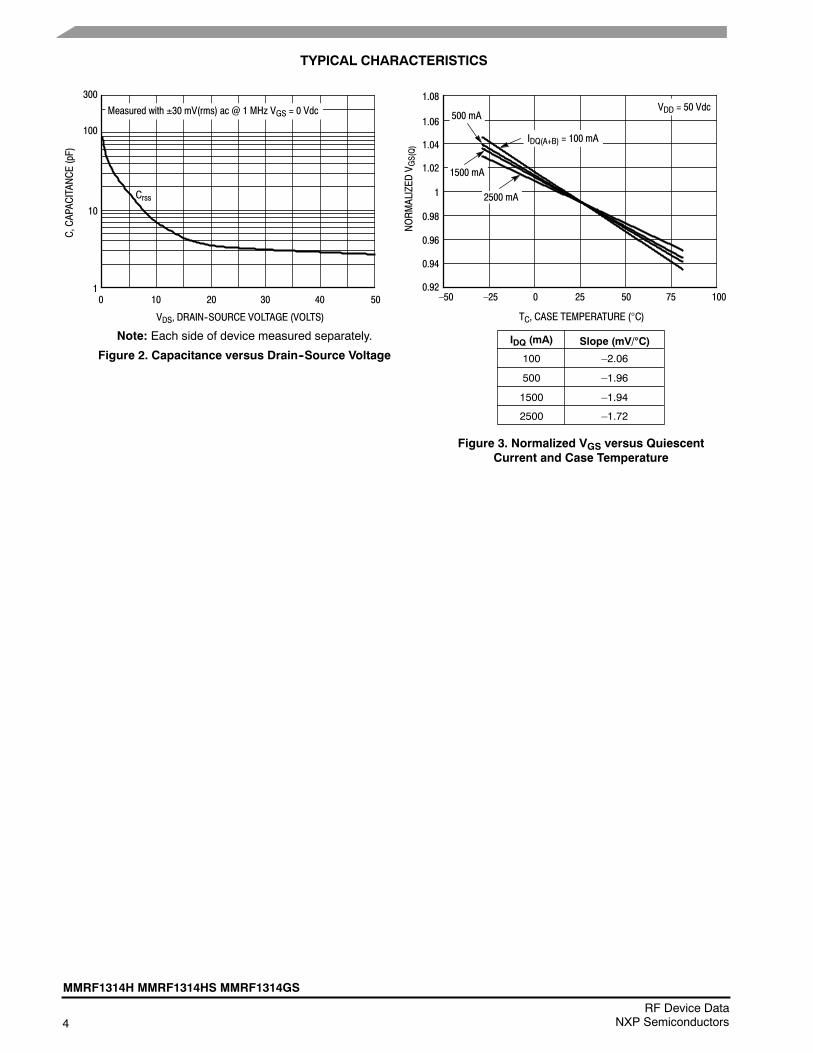
TYPICAL CHARACTERISTICS
500 2010
VDS, DRAIN--SOURCE VOLTAGE (VOLTS)
Figure 2. Capacitance versus Drain--Source Voltage
C,CAPACITANCE(pF)
30
10
140
Crss
100
Measured with ±30 mV(rms) ac @ 1 MHz VGS = 0 Vdc
IDQ(A+B) = 100 mA
Figure 3. Normalized VGS versus QuiescentCurrent and Case Temperature
NORMALIZED
V GS(Q)
TC, CASE TEMPERATURE (°C)
1.06
1.04
1.02
1
0.98
0.96
0.94
100–50 0–25 25 50 75
500 mA
1500 mA
2500 mA
VDD = 50 Vdc
100 –2.06
IDQ (mA) Slope (mV/°C)
500 –1.96
1500 –1.94
2500 –1.72
0.92
1.08300
Note: Each side of device measured separately.

MMRF1314H MMRF1314HS MMRF1314GS
5RF Device DataNXP Semiconductors
1200–1400 MHz REFERENCE CIRCUIT — 3.0″ × 4.0″ (7.6 cm × 10.2 cm)
C21
+
C23
C2
C8 L2
C6*
C32*
C33*C9*
C19
C7
C14
Figure 4. MMRF1314H(HS) Reference Circuit Component Layout — 1200–1400 MHz
* C3, C6, C9, C10, C11, C32 and C33 are mounted vertically.
Coax1
C12C13
R1
R2
C15
C16
C1
C17
C24
C20 C22
C10*
C11*
C4 C5
C31
C27C28
C29
C30
C25 C26
Q1C3*
C18
L1
Coax3
D80014Rev. 0
+
+
+
Coax2 Coax4
+
+
Table 6. MMRF1314H(HS) 1200–1400 MHz Reference Circuit Component Designations and ValuesPart Description Part Number Manufacturer
C1, C2 13 pF Chip Capacitors ATC800B130JT500XT ATC
C3, C6 3.9 pF Chip Capacitors ATC800B3R9CT500XT ATC
C4, C7 6.2 pF Chip Capacitors ATC800B6R2BT500XT ATC
C5, C8 2.0 pF Chip Capacitors ATC800B2R0BT500XT ATC
C9 2.7 pF Chip Capacitor ATC800B2R7BT500XT ATC
C10, C11, C32, C33 7.5 pF Chip Capacitors ATC800B7R5JT500XT ATC
C12, C15 22 μF, 25 V Tantalum Capacitors TPSD226M025R0200 AVX
C13, C16 2.2 μF Chip Capacitors C1825C225J5RACTU Kemet
C14, C17, C20, C27 24 pF Chip Capacitors ATC100B240CT500XT ATC
C18, C19, C25, C26 470 μF, 63 V Electrolytic Capacitors MCGPR63V477M13X26-RH Multicomp
C21, C28 2.2 μF Chip Capacitors C3225X7R2A225KT TDK
C22, C29 1000 pF Chip Capacitors ATC100B102JT50XT ATC
C23, C30 0.022 μF Chip Capacitors C1825C223K1GACTU Kemet
C24, C31 0.10 μF Chip Capacitors C1812F104K1RACTU Kemet
Coax1, 2, 3, 4 35 Ω Semi-flexible Coax Cable, 1.5″ Shield Length HSF-141C-35 Hongsen Cable
L1, L2 3.7 nH Inductors, 1 Turn GA3092-ALC Coilcraft
Q1 RF Power LDMOS Transistor MMRF1314H NXP
R1, R2 1000 Ω, 1/2 W Chip Resistors CRCW20101K00FKEF Vishay
PCB Arlon 450 0.030″, εr = 4.5 D80014 MTL

6RF Device Data
NXP Semiconductors
MMRF1314H MMRF1314HS MMRF1314GS
TYPICAL CHARACTERISTICS — 1200–1400 MHzREFERENCE CIRCUIT
Gps,POWER
GAIN(dB)
14001200
IRL
f, FREQUENCY (MHz)
Figure 5. Power Gain, Drain Efficiency and IRLversus Frequency at a Constant Input Power
13251300127512501225
19
18
–16
60
50
–6
ηD,DRAIN
EFFICIENCY(%)
ηD
16.5
16
13.5
12.5
18.5
17.517
40
15.515
1350 1375
VDD = 52 Vdc, Pin = 25 W, IDQ(A+B) = 100 mAPulse Width = 128 μsec, Duty Cycle = 10%
55
45
35–4
–8
IRL,INPUTRETURN
LOSS
(dB)
1414.5
13–12–10
–14
10
24
20
70
Pout, OUTPUT POWER (WATTS) PEAK
Figure 6. Power Gain and Drain Efficiency versusOutput Power
8000
22
18
16
14
60
50
40
30
ηD,DRAINEFFICIENCY(%)
Gps
ηD
Gps,POWER
GAIN(dB)
200 400 600 1000
20
12 10
01200 1400 1600
800
1300
120040
1225
1200
1100
56
52
f, FREQUENCY (MHz)
P out,OUTPUTPOWER
(WATTS)PEAK
ηD,DRAINEFFICIENCY(%)
1250
900
1000
60
48
44
1275 1300 1325 1350 1375 1400
ηD
Figure 7. Output Power and Drain Efficiency versusFrequency at a Constant Input Power
65
1200 MHz
1400 MHz
1300 MHz
1300 MHz
1200 MHz
1400 MHz
VDD = 52 Vdc, IDQ(A+B) = 100 mAPulse Width = 128 μsec, Duty Cycle = 10%
VDD = 52 Vdc, IDQ(A+B) = 100 mA, Pin = 25 WPulse Width = 128 μsec, Duty Cycle = 10%
Gps
Pout
MMRF1314H MMRF1314HS MMRF1314GS
7RF Device DataNXP Semiconductors
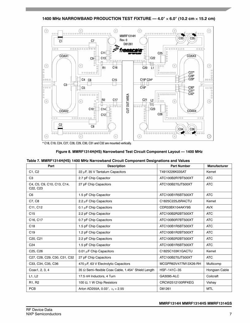
1400 MHz NARROWBAND PRODUCTION TEST FIXTURE — 4.0″ × 6.0″ (10.2 cm × 15.2 cm)
Figure 8. MMRF1314H(HS) Narrowband Test Circuit Component Layout — 1400 MHz
C4
C5
C1
C3
C9
C2
C7
C8
R1
R2
L1
L2
C6
C10
C11
C13
C14
C12
C15
C16
C17
C20
C22
C21
C23
C26
C25
C34 C36
C33 C35
C27*C28*C29*
C30*C31*C32*
MMRF1314HRev. 0D81261
* C18, C19, C24, C27, C28, C29, C30, C31 and C32 are mounted vertically.
CUTOUTAREA
COAX1
COAX2
COAX3
COAX4
C19*
C18*
C24*
Table 7. MMRF1314H(HS) 1400 MHz Narrowband Circuit Component Designations and ValuesPart Description Part Number Manufacturer
C1, C2 22 μF, 35 V Tantalum Capacitors T491X226K035AT Kemet
C3 2.7 pF Chip Capacitor ATC100B2R7BT500XT ATC
C4, C5, C9, C10, C13, C14,C22, C23
27 pF Chip Capacitors ATC100B270JT500XT ATC
C6 1.5 pF Chip Capacitor ATC100B1R5BT500XT ATC
C7, C8 2.2 μF Chip Capacitors C1825C225J5RACTU Kemet
C11, C12 0.1 μF Chip Capacitors CDR33BX104AKY9S AVX
C15 2.2 pF Chip Capacitor ATC100B2R2BT500XT ATC
C16, C17 0.7 pF Chip Capacitors ATC100B0R7BT500XT ATC
C18 1.5 pF Chip Capacitor ATC100B1R5BT500XT ATC
C19 1.2 pF Chip Capacitor ATC100B1R2BT500XT ATC
C20, C21 2.2 pF Chip Capacitors ATC100B2R2BT500XT ATC
C24 1.5 pF Chip Capacitor ATC100B1R5BT500XT ATC
C25, C26 0.01 μF Chip Capacitors C1825C103K1GACTU Kemet
C27, C28, C29, C30, C31, C32 27 pF Chip Capacitors ATC100B270JT500XT ATC
C33, C34, C35, C36 470 μF, 63 V Electrolytic Capacitors MCGPR63V477M13X26-RH Multicomp
Coax1, 2, 3, 4 35 Ω Semi--flexible Coax Cable, 1.454″ Shield Length HSF--141C--35 Hongsen Cable
L1, L2 17.5 nH Inductors, 4 Turn GA3095-ALC Coilcraft
R1, R2 100 Ω, 1 W Chip Resistors CRCW2512100RFKEG Vishay
PCB Arlon AD255A, 0.03″, εr = 2.55 D81261 MTL

8RF Device Data
NXP Semiconductors
MMRF1314H MMRF1314HS MMRF1314GS
TYPICAL CHARACTERISTICS — 1400 MHzPRODUCTION TEST FIXTURE
Pout, OUTPUT POWER (WATTS) PEAK
Figure 9. Power Gain and Drain Efficiencyversus Output Power
21
10 100
20 80
60
50
40
Gps,POWER
GAIN(dB)
ηD,DRAINEFFICIENCY(%)
ηD
14
1000
18
19
16
17
15
70
30
20
10
0
P3dB(W)
60
29
56
54
Pin, INPUT POWER (dBm) PEAK
Figure 10. Output Power versus Input PowerP out,OUTPUTPOWER
(dBm
)PEAK
58
50
48
52
31 33 35 37 39 41 43 45
46
62
1400 948 1079
f(MHz)
P1dB(W)
VDD = 50 Vdc, IDQ(A+B) = 100 mA, f = 1400 MHzPulse Width = 128 μsec, Duty Cycle = 10%
Gps
VDD = 50 Vdc, IDQ(A+B) = 100 mA, f = 1400 MHzPulse Width = 128 μsec, Duty Cycle = 10%
13
12
90
44
14
22
10 100
Pout, OUTPUT POWER (WATTS) PEAK
Figure 11. Power Gain versus Output Power
Gps,POWER
GAIN(dB)
1000
20
18
16
12
300 mA
100 mA
500 mA
IDQ(A+B) = 700 mA
14
10 100
Pout, OUTPUT POWER (WATTS) PEAK
Figure 12. Power Gain versus Output Power
Gps,POWER
GAIN(dB)
20
1000
18
IDQ(A + B) = 100 mA, f = 1400 MHz,Pulse Width = 128 μsec, Duty Cycle = 10%
16
10
12
50 V
Pin, INPUT POWER (dBm) PEAK
Figure 13. Output Power versus Input Power
P out,OUTPUTPOWER
(WATTS)PEAK
290
200
400
600
800
1000
1200
1400
33 35 37 39 41 43 45 30
25
65
100
55
Pout, OUTPUT POWER (WATTS) PEAK
Figure 14. Power Gain and Drain Efficiency versusOutput Power
Gps,POWER
GAIN(dB)
ηD,DRAINEFFICIENCY(%)
ηD
23
1000
45
21
19
17 35
Gps
13
11
15
35 V35 V
40 V
45 V
VDD = 30 V
TC = –40_C
VDD = 50 Vdc, IDQ(A+B) = 100 mA, f = 1400 MHzPulse Width = 128 μsec, Duty Cycle = 10%
25_C25_C
85_C
3127
VDD = 50 Vdc, IDQ(A+B) = 100 mA, f = 1400 MHzPulse Width = 128 μsec, Duty Cycle = 10%
TC = –40_C
85_C
25_C 85_C
25_C –40_C
0
15
VDD = 50 Vdc, f = 1400 MHzPulse Width = 128 μsec, Duty Cycle = 10%
2000
2000 2000
2000

MMRF1314H MMRF1314HS MMRF1314GS
9RF Device DataNXP Semiconductors
1400 MHz NARROWBAND PRODUCTION TEST FIXTURE
fMHz
ZsourceΩ
ZloadΩ
1400 7.35 – j4.62 1.3 – j.072
Zsource = Test circuit impedance as measured fromgate to gate, balanced configuration.
Zload = Test circuit impedance as measuredfrom drain to drain, balanced configuration.
Figure 15. Narrowband Series Equivalent Source and Load Impedance — 1400 MHz
InputMatchingNetwork
DeviceUnderTest
OutputMatchingNetwork
Zsource Zload
--
+
+
--
50Ω50Ω

10RF Device Data
NXP Semiconductors
MMRF1314H MMRF1314HS MMRF1314GS
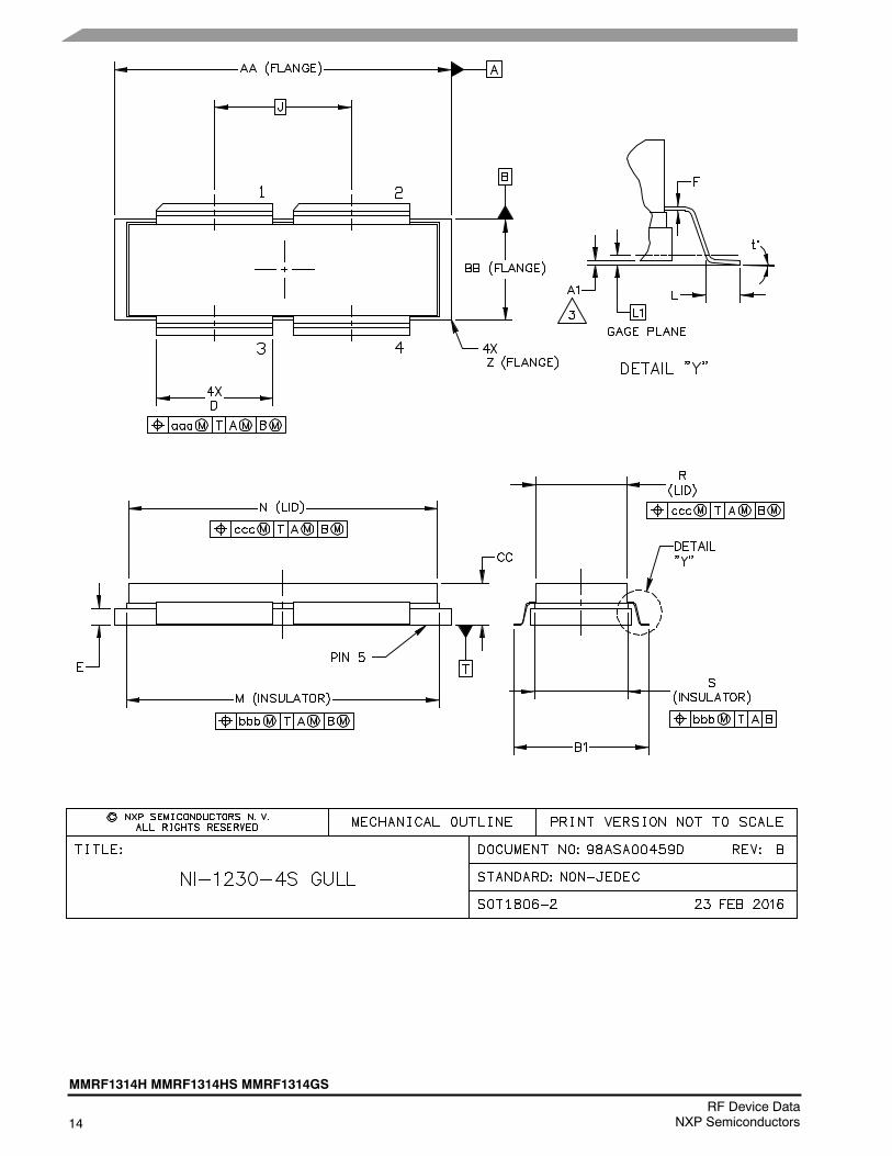
PACKAGE DIMENSIONS

MMRF1314H MMRF1314HS MMRF1314GS
11RF Device DataNXP Semiconductors

12RF Device Data
NXP Semiconductors
MMRF1314H MMRF1314HS MMRF1314GS

MMRF1314H MMRF1314HS MMRF1314GS
13RF Device DataNXP Semiconductors
14RF Device Data
NXP Semiconductors
MMRF1314H MMRF1314HS MMRF1314GS

MMRF1314H MMRF1314HS MMRF1314GS
15RF Device DataNXP Semiconductors

16RF Device Data
NXP Semiconductors
MMRF1314H MMRF1314HS MMRF1314GS
PRODUCT DOCUMENTATION AND SOFTWARE
Refer to the following resources to aid your design process.
Application Notes• AN1908: Solder Reflow Attach Method for High Power RF Devices in Air Cavity Packages
• AN1955: Thermal Measurement Methodology of RF Power Amplifiers
Engineering Bulletins• EB212: Using Data Sheet Impedances for RF LDMOS Devices
Software
• Electromigration MTTF Calculator
To Download Resources Specific to a Given Part Number:1. Go to http://www.nxp.com/RF
2. Search by part number
3. Click part number link
4. Choose the desired resource from the drop down menu
REVISION HISTORY
The following table summarizes revisions to this document.
Revision Date Description
0 Mar. 2016 • Initial Release of Data Sheet
1 Jan. 2017 • 1200–1400 MHz reference circuit: added performance data and graphs, reference circuit component layoutand component designations, pp. 5–6

MMRF1314H MMRF1314HS MMRF1314GS
17RF Device DataNXP Semiconductors
How to Reach Us:
Home Page:nxp.com
Web Support:nxp.com/support
Information in this document is provided solely to enable system and softwareimplementers to use NXP products. There are no express or implied copyright licensesgranted hereunder to design or fabricate any integrated circuits based on the informationin this document. NXP reserves the right to make changes without further notice to anyproducts herein.
NXP makes no warranty, representation, or guarantee regarding the suitability of itsproducts for any particular purpose, nor does NXP assume any liability arising out of theapplication or use of any product or circuit, and specifically disclaims any and all liability,including without limitation consequential or incidental damages. “Typical” parametersthat may be provided in NXP data sheets and/or specifications can and do vary indifferent applications, and actual performance may vary over time. All operatingparameters, including “typicals,” must be validated for each customer application bycustomer’s technical experts. NXP does not convey any license under its patent rightsnor the rights of others. NXP sells products pursuant to standard terms and conditions ofsale, which can be found at the following address: nxp.com/SalesTermsandConditions.
NXP, the NXP logo, Freescale, and the Freescale logo are trademarks of NXP B.V.All other product or service names are the property of their respective owners.E 2017 NXP B.V.
Document Number: MMRF1314HRev. 1, 1/2017