Embed Size (px)
Citation preview

1
CASE STUDY 2
RF WIRELESS TRANCEIVER –
SIMULATION AND ANALYSIS
AKOMA, CHIEMELE OGECHUKWU (11065981)
MODULE CODE: CTP 149N MODULE NAME: MICROWAVES AND OPTICAL COMMUNICATIONS
FACULTY OF COMPUTING
LONDON METROPOLITAN UNIVERSITY
166-220 HOLLOWAY ROAD N7 8DB
LONDON, UK

2
ABSTRACT
An RF wireless transceiver system is designed in this case study. The transmitter system is a one
stage Intermediate frequency (IF) superheterodyne transmitter, with a baseband frequency of
300MHz. The receiver uses a two stage IF downconverter, downconverting the RF first to
1000MHz and finally to 300MHz. The received power at PORT2 is 10.402dBm. Analyses
showed that as the link distance increased from 0.5-2.5Km, the received power decreased from
16.054-2.538 dBm; the decrease is almost linear. Also, a linear increase in Transmitter antenna
gain (TxGain) with received power (IFout). From budget power gain analysis, link1 showed the
highest loss in power while amp2 showed the highest gain. Link1 and Amp2 showed a high
contribution in noise figure (6.380 and 19.015) to the system.

3
OBJECTIVES OF THE EXPERIMENT
Create a system project for an RF transmitter using behavioral models (filter, amplifier,
mixer)
Use an RF source, LO with phase noise, and a noise controller
Perform a Harmonic Balance simulation
Analyze the system spectra
Perform System Budget analysis
Analyze the effect of the line-of-sight parameters on the system performance

4
BACKGROUND THEORY
RF WIRELESS TRANSCEIVER
A transceiver is any device comprising both a transmitter and a receiver which are combined and
share common circuitry or a single housing. The figure below shows the block diagram of an RF
wireless Transceiver, showing the transmitter, wireless link and the receiver. Transceivers enable
duplex communication modes (half or full). Various applications of transceivers include
WLANs, GPS, RF-Identification systems (RF-IDs), Home Satellite Networks, GSM, Satellite
Phones, Bluetooth devices, pagers, etc. Transceiver circuits are been implemented with IC chips,
in a drive towards miniaturization, cost and linearity [1-2].
Figure 1: A wireless transceiver system
Figure 2: A communication system

5
TRANSMITTER
The transmitter must produce a signal that has enough power, have generally a very accurate
frequency, and has a clean enough spectrum so that the transmitter does not disturb users of other
radio systems. Information to be transmitted, the baseband signal, is attached to a sinusoidal
carrier signal by modulating the carrier amplitude, frequency, or phase either analogically or
digitally [3]. There two basic types of transmitters, these are direct conversion (homodyne)
transmitter and superheterodyne (two or more steps) transmitter.
a. Direct conversion (homodyne) transmitter
Figure 3: Block diagram of a Direct conversion transmitter with phase-locked loop
Figure 2 presents a direct-conversion transmitter. A digital baseband signal (fref)
modulates the carrier in an IQ-modulator. The modulated signal is then filtered and
amplified [3].
b. Superheterodyne transmitter
Figure 4: block diagram of a superheterodyne transmitter
Superheterodyne transmitters are more complex than direct conversion transmitters. The
information signal modulates an intermediate frequency (IF) signal then converted to the
transmit relative frequency by a mixer. An IF filter is needed to eliminate the local
oscillator harmonics after the modulation. An RF filter is required at the mixer output to
move out the undesirable sideband. After stages for correction, equalization and
sometimes amplification, the IF signal is converted to an RF signal by a stage
named frequency mixer or frequency converter [4-5]. The superheterodyne transmitter is
based on the heterodyne principle.
CHANNEL
The channel in the communication system refers to the medium through which the information
transmitted from the transmitter sub-system to the receiver sub-system. This could either be air
medium, optical fibre, twisted pair, copper wire, coaxial cable, wave guide, etc [3].

6
Factors affecting radio range include antenna (gain, sensitivity to body effects, etc), sensitivity,
output power, radio pollution (selectivity, blocking, IP3) and environment (line-of-sight,
obstruction, reflections, multipath fading. The following can increase the range of the transceiver
systems, increasing the output power (eg adding an external power amplifier), increasing the
sensitivity, increasing both output power and sensitivity, and using high gain antennas [11].
Signal strength: A strong source signal allows for better reception over long distances than a
weak source signal. But the FCC limits unlicensed signal transmission strength to one watt
maximum and six dB watts of EIRP. Effectively, this allows for a maximum signal gain
equivalent to four watts. A signal conditioner at the receiving end can be used to enhance the
signal-to-noise performance by an order of magnitude [12].
Distance: RF signal strength decreases with distance. Also, the potential interference and signal
fading increases with distance [12].
Interference: sources of atmospheric interference can be rain, snow, hail or lightening in the
signal path. RF interference normally results from other nearby RF activity in the same band (in-
band interference). Only very strong out-of-band activity can interfere with a 2.4 GHz signal
[12].
Line of sight: RF line of sight requires a wider band of free-space signal path than visual line of
sight. Signal clarity is best when the line of sight between antennas is precisely focused and free
of all obstructions. Obstructions within the RF line of sight can absorb the signal and sap it of
strength or deflect the signal and cause multiple copies of the same signal to arrive at the receiver
out of phase. The success of an RF link depends on a clear line of sight. An unobstructed line of
sight is called a free space path. An acceptable line-of-sight for an RF signal is defined as at least
.6 clearance in the first Fresnel zone. This means that for successful RF transmission, at least 60
percent of the area between the center lobe and the bottom of the first Fresnel zone must be a
free-space path. A large obstruction can reduce or totally block the signal. The bending of signals
as they pass around obstructions or are deflected by them is known as diffraction. A reduction of
the strength of a signal is known as attenuation . Factors affecting line-of-sight include free space
loss, attenuation and scattering, atmospheric absorption, ducting, multipath and fading, refraction
and reflection [11-12].
Equation for free space path loss is given by
Free space path loss (dB) = 27.6(dB) – 20log[frequency(MHz)] – 20log[distance(m)]

7
Figure 5: Graph of Attenuation against Frequency showing attenuation by various components
for different frequencies.
RECEIVER
The receiver subsystem receives the signal and converts it back to usable form, either visual (as
in television), audio (as in FM or AM), or data (for computers, etc). A receiver should be able to
select the desired signal, and distinguish very weak signals from noise and other unwanted
signals lying in the band [8].
Frii’s transmission equation for free space propagation is given by
Where Pt is the transmitted power, Pr is the received power, Gt and Gr is the transmitter and
receiver antenna gain respectively, λ is the wavelength and d is the distance between transmitter
and receiver or the range. [11].

8
Figure 6: Simulated Operation of a receiver
Most popular architectures for receivers are Heterodyne, Homodyne, Wideband-IF and Low-IF
[8].
Heterodyne Architecture
Super-heterodyne is the most widely used architecture in wireless transceivers so far. It is a dual
conversion architecture, in which, at the first state RF is down-converted to IF and then, in
second stage it is from IF to baseband signal. The block diagram of super-heterodyne receiver
architecture is shown in Figure 3. From the incoming RF signal preselection filter removes out of
band signal energy as well as partially reject image band signals. It is then amplified by LNA to
supress the contribution of noise from the succeeding stages. Image Reject filter attenuates the
signals at image band frequencies coming from LNA. Mixer-I downconverts the signal coming
out of the IR filter from RF frequency to IF frequency with the output of a Local Oscillator. The
channel selection is normally achieved through IF filter: It is a BP filter to allow the IF band of
interest and other band is rejected. This filter is critical in determining the sensitivity and
selectivity of a receiver [9-10].

9
Figure 7: Block diagram of a typical Heterodyne Receiver
Since channel selection is done at IF1, the LO requires an external tank for good phase noise
performance. In case of phase or frequency modulation, downconversion to the baseband
requires both in-phase(I) and quadrature(Q) components of the signal. Mixer-II does the second
down conversion of IF signal into I and Q components for digital signal processing. The LP filter
acts as a channel reject filter along with job of anti-aliasing functionality [9-10].
Trade-offs
IR filter and channel selection.
Good sensitivity and selectivity [9-10].
Drawbacks
High Q filter
High performance oscillator or LO
LNA output impedance matched to 50 ohm is difficult.
Integration of HF image reject filter is a major problem [9-10].
Homodyne Architecture
Homodyne receivers translates the channel of interest directly from RF to baseband (ωIF=0) in a
single stage. Hence these architectures are called Direct IF architectures or Zero-IF architectures.
For frequency and phase modulated signals, down conversion must provide quadrature outputs
so as to avoid loss of information [9-10]. The block diagram of heterodyne architecture is
illustrated in Figure 4.
Figure 8: Block diagram of Homodyne Receiver Architecture
Merits of Zero-IF architecture are
Less hardware
No image problem. So image filter not required.
Because of no IF stage, LPF is sufficient for filtering.
Amplification at BB stage. Hence power saving.
In integrated circuits LNA need not to match to 50 ohm. Because no image reject filter
between LNA and mixer [9-10].

10
De-merits of Zero-IF architecture are
LO Leakage: Generally there will be an imperfect isolation between LO port and input
port of mixer and LNA, due to capacitve and substrate coupling. Because of this there
will be LO feed though from LO port to the input port of the mixer and LNA. This LO
leakage mixes with original LO, called self-mixing, produces DC offsets in the mixer
output and causes saturation of following stages in the receiver chain.
DC offset errors: It is the most serious problem in the baseband section of the homodyne
receivers. The cause of it is self mixing of LO leakage which is due to LO feed through to
mixer input port and LNA and insufficient isolation between LO port to mixer input port
and LNA input.
Since LO frequency is same as carrier frequency, it leaks from receiver to antenna which
interferes with same frequency-band receivers.
Flicker noise from an active device contaminate the BB signal.
I/Q mis-match
Even order distortion [9-10]
Wideband-IF Architecture
Wideband-IF receiver is a dual conversion architecture in which data is downconverted from RF
to IF in the 1st stage, and in the 2nd stage it is from IF to Baseband [9-10]. The block diagram of
Wideband-IF receiver architecture is shown in Figure 5.
Figure 9: Block diagram of Wideband-IF Receiver Architecture
In this architecture all the RF channels are complex mixed and downconverted to fixed IF after
preselection filtering and amplification. In second stage an Image Reject (IR) mixer does
complex mixing and translate IF to BB using a tunable channel select frequency synthesizer. All
the image frequencies are cancelled by IR mixer. If the IF is chosen high enough, additional
image rejection may be obtained from the RF front-end preselection filter. Channel selection is
performed at baseband by using programmable integrated channel select filter. Since LO-1 is
fixed frequency synthesizer generated by crystal controlled oscillator good phase noise
performance is obtained. Channel tuning is achieved by using programmable frequency
synthesizer at IF [9-10].
Low-IF Architecture
In Low-IF receiver architecture all the RF signals are translated to low-IF frequency which is
then down-converted to BB signal in digital domain. Low-IF architecture comprises the

11
advantages of both heterodyne and homodyne receivers [9-10]. The block diagram of Low-IF
receiver architecture is shown in Figure 6.
Figure 10: Block diagram of Low-IF Receiver Architecture
After preselection filtering and amplification, all the RF channels are quadrature mixed and
downconverted to low IF containing both wanted and unwanted signals. The IF frequency is just
one or two channels bandwidth away from DC, which is just enough to overcome DC offset
problems. It is then amplified and filtered before sampled by ADC. Since the ADC samples both
wanted and unwanted signals, there will be higher demand on ADC dynamic range requirements.
The ac-coupled signal path to ADC eliminates the need of DC offset compensation circuitry. The
sampled digital data is fed to image reject mixer which is implemented in digital domain [9-10].
HETERODYNING
Heterodyning technique was invented in 1901 by Reginald Fessenden. In heterodyning, two
frequencies are mixed or combined to create a new frequency range. It is used in shifting a
frequency into a new frequency range. The two frequencies, f1 and f2, are combined using a non-
linear device called a mixer (which could be a diode or transistor). The new frequencies
generated from the non-linear mixing consist of two frequencies, that is, the sum (f1 + f2) and the
difference (f1 – f2). These frequencies are call heterodynes or beat frequencies. The analysis of
the frequency spectrum from the mixer output shows the f1+f2, f1-f2, harmonics of f1, harmonics
of f2, beat frequencies of the interactions of the various harmonics. In most situations, one of the
two frequencies is desired; the other is filtered out at the output of the mixer [4, 13].
Mathematically, heterodyning can be expressed thus,
When two sine wave signals, sin (2πf1t) and sin (2πf2t), are multiplied, using trigonometric
identity,
This is result shows the two intermediate frequencies (the sum and difference of the two original
frequencies).
Three reasons for the use of Intermediate frequency (IF) in RF circuits include:
1. At very high (gigahertz) frequencies, signal processing circuitry performs poorly. Active
devices such as transistors cannot deliver much amplification (gain) without becoming
unstable. Ordinary circuits using capacitors and inductors must be replaced with
cumbersome high frequency techniques such as striplines and waveguides. So a high
frequency signal is converted to a lower IF for processing.
2. A second reason to use an IF, in receivers that can be tuned to different stations, is to
convert the various different frequencies of the stations to a common frequency for

12
processing. It is difficult to build amplifiers, filters, and detectors that can be tuned to
different frequencies, but easy to build tunable oscillators. Superheterodyne receivers tune
in different stations simply by adjusting the frequency of the local oscillator on the input
stage, and all processing after that is done at the same frequency, the IF. Without using an
IF, all the complicated filters and detectors in a radio or television would have to be tuned in
unison each time the station was changed, as was necessary in the early tuned radio
frequency receivers.
3. An important use of intermediate frequency is to improve frequency selectivity. In
communication circuits, a very common task is to separate out or extract signals or
components of a signal that are close together in frequency. This is called filtering. Some
examples are, picking up a radio station among several that are close in frequency, or
extracting the chrominance subcarrier from a TV signal. With all known filtering techniques
the filter's bandwidth increases proportionately with the frequency. So a narrower bandwidth
and more selectivity can be achieved by converting the signal to a lower IF and performing
the filtering at that frequency [11].
Applications of IF (heterodyning)
Heterodyning is used very widely in communications engineering to generate new frequencies
and move information from one frequency channel to another. it is used in radio transmitters,
modems, satellite communications and set-top boxes, radar, radio telescopes, telemetry systems,
cell phones, cable television converter boxes and headends, microwave relays, metal detectors,
atomic clocks, and military electronic countermeasures (jamming) systems, analog tape recorder
and music synthesis [4].
Advantages of superheterodyne includes
In transmitters several correction and equalization stages are used after modulation. In direct
modulation these stages must be developed separately for each output RF (so called
channel). On the other hand, in superheterodyne transmitters since a single intermediate
frequency signal is used, only one type of stage for IF is developed. Thus the said stages are
more reliable in superheterodyne. Also R&D is much easier for the designer.
Operators may change the RF output of the transmitter. In direct modulation, it is very
difficult to change the RF output. Because in this case, practically all stages need to be
retuned for the new RF. On the other hand in superheterodyne only the output stages need to
be retuned [4].
COMPONENTS OF TRANSMITTER/RECEIVER SUBSYTEM
RF MIXERS
An RF mixer is a 3-port non-linear device. It is any passive or active device that converts a
frequency to another. A mixer can be used to modulate, demodulate a signal or even as a phase
detector [11-12]. Figure 5 shows an ideal mixer.

13
Figure 11: An ideal mixer
The mixer takes an RF signal at RF input, combines it with the signal from the local oscillator
(LO) at LO input, to produce an intermediate frequency (IF) at the IF output port. It is at the
mixer that heterodyning (as explained above) is done [11-12].
When the sum of the LO and RF is required, the mixer is called an upconverter (this is used in
transmitter circuits); but when the difference of LO and R Fir required, the mixer is called a
downconverter (this is used in receiver circuits). Low-side injection occurs when the LO
frequency is less than the RF frequency; the reverse is called high-side injection. Another
important to note in an RF is that each output is half (½) of the individual inputs. Therefore,
there would a loss of 6dB in an ideal mixer [12]
Figure 12: Output spectrum of an up-conversion mixer system
Important Mixer properties are: Conversion Gain or Loss, Intercept point, Isolation, Noise
Figure, High-order spurious response rejection and Image noise suppression [14].
1. Conversion Gain or Loss of the RF Mixer is dependent by the type of the mixer (active or
passive), load of the input RF circuit, output impedance at the RF port, the level of the
LO. The typical conversion gain of an active Mixer is approximately +10dB when the
conversion loss of a typical diode mixer is approximately -6dB. The Conversion Gain or
Loss of the RF Mixer measured in dB is given by:
Conversion (dB) = Output IF power delivered to the load (dBm) – Available RF input signal power (dBm)
2. Input Intercept Point (IIP3) is the RF input power at which the output power levels of the
unwanted intermodulation products and the desired IF output would be equal. The Third-
Order intercept point (IP3) in a Mixer is defined by the extrapolated intersection of the

14
primary IF response with the two-tone third-order intermodulation IF product that results
when two RF signals are applied to the RF port of the Mixer.
3. Spurious products in a Mixer are problematic, and Mixer vendors frequently provide
tables showing the relative amplitudes of each response under given LO drive conditions.
4. Isolation is the amount of local oscillator power that leaks into either the IF or the RF
ports. There are multiple types of isolation: LO-to-RF, LO-to-IF and RF-to-IF isolation.
5. Noise Figure is a measure of the noise added by the Mixer itself, noise as it gets
converted to the IF output or is a measure of how much the signal-to-noise ratio (SNR)
degrades as the signal passes through the block. It is defined as
where PO is the total output noise power, PL is the output noise power that results from
noise generated by the load at the output frequency, and PS is the output noise power that
results from noise generated by the source at the input frequency.
For a passive Mixer which has no gain and only loss, the Noise Figure is almost
equal with the loss.
In a mixer noise is replicated and translated by each harmonic of the LO that is
referred to as Noise Folding [14].
Present also in the mixer frequency spectrum is the image frequency. This is given by the
formula,
fimage = frf + 2(I.F)
A good choice of LO and IF frequencies would help to reduce the effect of image frequency as it
can negatively affect the RF frequency [14].
FILTER Filter circuits can be used to separate or combine different frequencies, reject unwanted frequencies while permitting the transmission of a wanted frequency. Filters are used to select or confine specific
frequencies within the allotted Spectruml limits. Example of such circuits where a filter can be found
includes multiplexers, demultiplexers, transmitter and receiver circuits, etc. Filters can be classified into low pass filter (LPF), high pass filter (HPF), band pass filter (BPF) and band stop filter (BSF) [14-15].
Figure 7(a) shows the idealized filter responses of filters, with the shaded region indicating the
allowed (or pass band) frequencies. Since it is almost impossible to realize such an ideal filter
response with an infinite stopband attenuation and instantaneous transition from pass band to

15
stopband, figure 7(b) shows a typical response of a lowpass filter. Five practical filter parameters
are shown in figure 7(b)
(a) (b)
Figure 13: (a) Idealized filter responses; (b) Realistic low pass filter response showing key filter parameters
There various standard filter responses. This varies with filter transfer functions and could affect
filter complexity and cost [14]. They are as follows:
Butterworth
It is also known as the maximally flat filter as it has no ripple in the pass band or stopband. It has
the best compromise between attenuation and phase response. It has a relatively wide transition
region with average transient characteristics [14]. The equation for the pole positions is
(Where k is the pole pair number and n is the number of poles)
Chebyshev
The chebyshev filter for the same order butterworth filter, has a smaller transition region, but at
the expense of ripples in its pass band. The number of ripples equals the order of the filter [14].
Bessel The Bessel filter is optimized for better transient response of linear phase in the pass band. This
implies a relatively poor frequency response. The poles are determined by locating the poles on a
circle and then separate the imaginary parts by ; where n is the number of poles [14].
Elliptical
The presence of ripples in both pass band and stopband of the elliptical filter gives it a shorter
transition region than the chebyshev filter (since zeros are in the stopband) [14].
Other response types include Gaussian and inverse chebyshev filter responses [14].

16
Figure 14: Comparison of amplitude response of Bessel, butterworth and chebyshev filters.
POWER AMPLIFIER (OP AMP)
An RF power amplifier is an example of an electronic amplifier. It is used in converting a low-
power radio-frequency signal into a larger signal of significant power, typically for driving the
antenna of a transmitter. It is optimized to have high efficiency, high output Power (P1dB)
compression, good return loss on the input and output, good gain, and optimum heat dissipation.
Applications of RF power amplifier include Wireless Communication, TV transmissions, Radar,
and RF heating, and exciting resonant cavity structures [15-16].
RF power can be classified in classes A, B, AB, C, D, E and F. Important parameters that defines
an RF Power Amplifier include: Output Power, Gain, Linearity, Stability, supply voltage,
Efficiency, and Ruggedness. The level of performance of an rf power amplifier can be
determined by choosing the bias points. By comparing PA bias approaches, one can evaluate the
trade-offs for: Output Power, Efficiency, Linearity, or other parameters for different applications
[16].
The Power Class of the amplification determines the type of bias applied to an RF power
transistor. The Power Amplifier’s Efficiency is a measure of its ability to convert the DC power
of the supply into the signal power delivered to the load.
The definition of the efficiency can be represented in an equation form as:
Power that is not converted to useful signal is dissipated as heat. Power Amplifiers that has low
efficiency have high levels of heat dissipation, which could be a limiting factor in particular
design. Other factors affecting Power Amplifier output include dielectric and conductor losses
[16].
When two or more signals are input to an amplifier simultaneously, the second, third, and higher-
order intermodulation components (IM) are caused by the sum and difference products of each of
the fundamental input signals and their associated harmonics [16]. These are
Fundamental: f1, f2
Second order: 2f1, 2f2, f1 + f2, f1 - f2
Third order: 3f1, 3f2, 2f1 ± f2, 2f2 ± f1,
Fourth order: 4f1, 4f2, 2f2 ± 2f1,
Fifth order: 5f1, 5f2, 3f1 ± 2f2, 3f2 ± 2f1, + Higher order terms
17
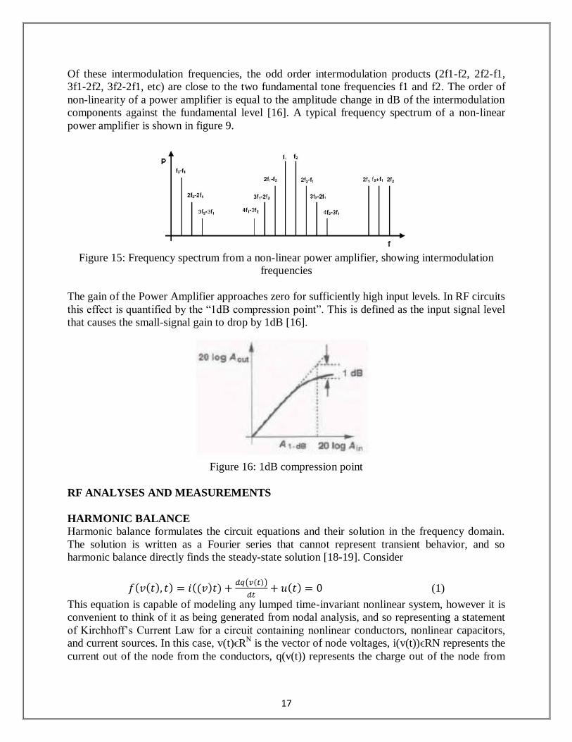
Of these intermodulation frequencies, the odd order intermodulation products (2f1-f2, 2f2-f1,
3f1-2f2, 3f2-2f1, etc) are close to the two fundamental tone frequencies f1 and f2. The order of
non-linearity of a power amplifier is equal to the amplitude change in dB of the intermodulation
components against the fundamental level [16]. A typical frequency spectrum of a non-linear
power amplifier is shown in figure 9.
Figure 15: Frequency spectrum from a non-linear power amplifier, showing intermodulation
frequencies
The gain of the Power Amplifier approaches zero for sufficiently high input levels. In RF circuits
this effect is quantified by the “1dB compression point”. This is defined as the input signal level
that causes the small-signal gain to drop by 1dB [16].
Figure 16: 1dB compression point
RF ANALYSES AND MEASUREMENTS
HARMONIC BALANCE
Harmonic balance formulates the circuit equations and their solution in the frequency domain.
The solution is written as a Fourier series that cannot represent transient behavior, and so
harmonic balance directly finds the steady-state solution [18-19]. Consider
(1)
This equation is capable of modeling any lumped time-invariant nonlinear system, however it is
convenient to think of it as being generated from nodal analysis, and so representing a statement
of Kirchhoff’s Current Law for a circuit containing nonlinear conductors, nonlinear capacitors,
and current sources. In this case, v(t)ϵRN is the vector of node voltages, i(v(t))ϵRN represents the
current out of the node from the conductors, q(v(t)) represents the charge out of the node from

18
the capacitors, and u(t) represents the current out of the node from the sources. To formulate the
harmonic balance equations, assume that v(t) and u(t) are T-periodic and reformulate the terms
of (1) as a Fourier series [18].
It is in general impossible to directly formulate models for nonlinear components in the
frequency domain. To overcome this problem, nonlinear components are usually evaluated in the
time domain. Thus, the frequency domain voltage is converted into the time domain using the
inverse Fourier transform, the nonlinear component (i and q) is evaluated in the time domain,
and the current or charge is converted back into the frequency domain using the Fourier
transform [18].

19
METHODOLOGY
Figure 17: RF wireless Transceiver schematic in ADSTM

20
The schematic diagram shown above is for an RF wireless transceiver system, consisting of a
direct conversion transmitter system, link (channel) and a 2-stage heterodyne receiver. The
transmitter subsystem consists of the BaseBand (PORT1), a baseband up-converter mixer
(b1_MIX1), an RF bandpass butterworth filter (b2_BPF1), and an RF power amplifier
(b3_AMP1). The receiver subsystem consists of an RF bandpass butterworth filter (b5_BPF2),
two IF bandpass butterworth filters (b8_BPF3 and b9_2_BPF4), Low noise amplifier
(b6_AMP2), 2 IF – downconverter mixers (b7_MIX2 and b9_1_MIX3), and an IF Power
amplifier (b9_0_AMP3).
PART 1
The schematic components are connected as shown in figure 11 from the various libraries in the
ADSTM
component library palette.
PART 2
The baseband frequency of the system is given as 300MHz while the RF output frequency of the
system is given to be 19.5GHz. The chosen frequency for the three oscillators (LOfreq1,
LOfreq2 and LOfreq3) and centre frequency of the four bandpass filters (RFfreq, IFfreq1 and
IFfreq2) are shown in table 1 of Results and Analyses section.
PART 3
The following simulation tools where added to the schematic, HarmonicBalance, Options,
BudGain, BudFdeg, BudNF, BudPwrInc and Var, to test and analyze the performance of the
system. The Var component sets the variables in the system.
For Part 4 and Part 5 please see Results and Analyses
21
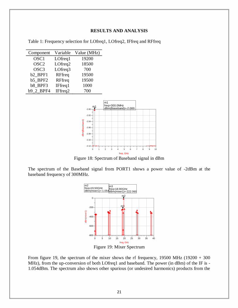
RESULTS AND ANALYSIS
Table 1: Frequency selection for LOfreq1, LOfreq2, IFfreq and RFfreq
Component Variable Value (MHz)
OSC1 LOfreq1 19200
OSC2 LOfreq2 18500
OSC3 LOfreq3 700
b2_BPF1 RFfreq 19500
b5_BPF2 RFfreq 19500
b8_BPF3 IFfreq1 1000
b9_2_BPF4 IFfreq2 700
Figure 18: Spectrum of Baseband signal in dBm
The spectrum of the Baseband signal from PORT1 shows a power value of -2dBm at the
baseband frequency of 300MHz.
Figure 19: Mixer Spectrum
From figure 19, the spectrum of the mixer shows the rf frequency, 19500 MHz (19200 + 300
MHz), from the up-conversion of both LOfreq1 and baseband. The power (in dBm) of the IF is -
1.054dBm. The spectrum also shows other spurious (or undesired harmonics) products from the
1 2 3 4 5 6 7 8 90 10
-2.10
-2.08
-2.06
-2.04
-2.02
-2.12
-2.00
freq, GHz
dB
m(B
ase
ba
nd
)
Readout
m1
m1freq=dBm(Baseband)=-2.000
300.0MHz
5 10 15 20 25 30 350 40
-600
-400
-200
-800
0
freq, GHz
dB
m(m
ixe
r1)
Readout
m2
Readout
m3
m2freq=dBm(mixer1)=-1.054
19.50GHzm3freq=dBm(mixer1)=-222.060
18.90GHz

22
mixing. Among the undesired harmonics is downconversion of LOfreq1 and baseband, (19200-
300MHz), 18900MHz; its power in dBm is -222.060
Figure 20: Filter1 spectrum
After the upconversion, a filter with a narrow bandwidth is needed to suppress all wanted
(spurious) frequencies and prevent them from being transmitted through the antenna, allowing
only the upconverted frequency to pass through. The spectrum of filter1 is shown in figure 20
above.
Figure 21: Amp1 spectrum
After filtering, the signal is then amplified to ensure that sufficient power is transmitted to the
antenna and subsequently through the antenna to the receiver. The signal received at the receiver
has to have sufficient power levels above the sensitivity of the receiver to ensure proper
reception of the transmitted signal.
5 10 15 20 25 30 35 40 45 50 550 60
-180
-160
-140
-120
-100
-80
-60
-40
-20
0
-200
20
freq, GHz
dB
m(f
ilte
r1)
Readout
m8
m8freq=dBm(filter1)=-1.054
19.50GHz
5 10 15 20 25 30 35 40 45 50 550 60
-180
-160
-140
-120
-100
-80
-60
-40
-20
0
20
-200
40
freq, GHz
dB
m(a
mp
1)
Readout
m11
m11freq=dBm(amp1)=27.763Max
19.50GHz
23
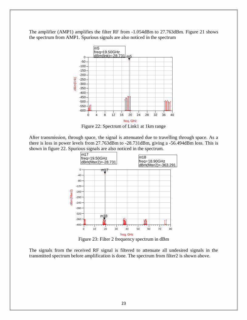
The amplifier (AMP1) amplifies the filter RF from -1.054dBm to 27.763dBm. Figure 21 shows
the spectrum from AMP1. Spurious signals are also noticed in the spectrum
Figure 22: Spectrum of Link1 at 1km range
After transmission, through space, the signal is attenuated due to travelling through space. As a
there is loss in power levels from 27.763dBm to -28.731dBm, giving a -56.494dBm loss. This is
shown in figure 22. Spurious signals are also noticed in the spectrum.
Figure 23: Filter 2 frequency spectrum in dBm
The signals from the received RF signal is filtered to attenuate all undesired signals in the
transmitted spectrum before amplification is done. The spectrum from filter2 is shown above.
4 8 12 16 20 24 28 32 360 40
-550
-500
-450
-400
-350
-300
-250
-200
-150
-100
-50
-600
0
freq, GHz
dB
m(l
ink)
Readout
m5
m5freq=dBm(link)=-28.731
19.50GHz
10 20 30 40 50 60 700 80
-360
-320
-280
-240
-200
-160
-120
-80
-40
-400
0
freq, GHz
dB
m(f
ilter2
)
Readout
m17
Readout
m18
m17freq=dBm(filter2)=-28.731
19.50GHz m18freq=dBm(filter2)=-363.291
18.90GHz

24
Figure 24: Amp2 frequency Spectrum
After the received signal is filtered, the signal is ready for amplification, due to the heavy
attenuation in transmission. Amp2 is a Low Noise Amplifier (LNA), whose function is to
amplify possible very weak signals received by the receiver’s antenna.
The received RF is amplified by Amp2 from -27.731dBm to -2.487dBm. The spectrum of Amp2
is shown in figure 24 above.
Figure 25: Mixer2 frequency spectrum in dBm
An IF is generated to the downconversion of mix2 of the RF, from 19500MHz to 1000MHz.
This is to enable the processing of the signal in the receiver. The desired IF generated has a
power level of -1.784dBm. The presence of spurious signals and intermodulation frequencies
noise is also seen in the spectrum shown in figure 25.
The Image frequency generated is
fimage = frf + 2(IF)
= 19500 + 2(1000) MHz
= 19500 + 2000 MHZ
= 21500 MHz (21.5 GHz)
5 10 15 20 25 30 350 40
-450
-400
-350
-300
-250
-200
-150
-100
-50
-500
0
freq, GHz
dB
m(a
mp
2)
Readout
m19
m19freq=dBm(amp2)=-2.487
19.50GHz
5 10 15 20 25 30 350 40
-700
-600
-500
-400
-300
-200
-100
-800
0
freq, GHz
dB
m(m
ixe
r2)
Readout
m20
Readout
m21
m20freq=dBm(mixer2)=-1.784
1.000GHzm21freq=dBm(mixer2)=-206.534
38.00GHz

25
Figure 26: Frequency spectrum of filter3 in dBm
Filter3 further attenuates all unwanted signals from the mixed frequency spectrum. The output of
filter3 spectrum is shown in figure 26 above.
Figure 27: frequency spectrum of Amp3 in dBm
Amp3 amplifies the filtered signal, attenuating all undesired frequencies present in the spectrum.
This is shown in figure 27 above.
5 10 15 20 25 30 350 40
-1400
-1300
-1200
-1100
-1000
-900
-800
-700
-600
-500
-400
-300
-200
-100
-1500
0
freq, GHz
dB
m(f
ilte
r3)
Readout
m22
20.20G-343.4
m23
m22freq=dBm(filter3)=-1.732
1.000GHzm23freq=dBm(filter3)=-1046.669
38.00GHz
5 10 15 20 25 30 350 40
-1400
-1300
-1200
-1100
-1000
-900
-800
-700
-600
-500
-400
-300
-200
-100
0
-1500
100
freq, GHz
dB
m(a
mp
3)
Readout
m24
m24freq=dBm(amp3)=17.402
1.000GHz

26
Figure 28: Frequency spectrum of mixer3 in dBm
In this final stage of downconversion, the IF is downconverted from 1000MHz to 300MHz, the
baseband frequency. The presence of intermodulation noise generated by this downconversion is
attenuated by filter4 before the signal is reconverted back the original form at port2. This is
shown in figure 29 below.
Figure 29: Frequency spectrum of IFout in dBm
FURTHER ANALYSIS
The effect of the link distance (range) on IFout was investigated and the result is shown in figure
30 below.
2 4 6 8 10
12
14
16
18
20
22
24
0 25
-1400
-1300
-1200
-1100
-1000
-900
-800
-700
-600
-500
-400
-300
-200
-100
0
-1500
50
freq, GHz
dB
m(m
ixe
r3)
Readout
m6
m6freq=dBm(mixer3)=10.402
300.0MHz
5 10 15 20 25 30 350 40
-1900-1800-1700-1600-1500-1400-1300-1200-1100-1000-900-800-700-600-500-400-300-200-100
-2000
0
freq, GHz
dB
m(I
Fo
ut)
Readout
m7
m7freq=dBm(IFout)=10.402
300.0MHz

27
Figure 30: A plot of Power received at receiver antenna (dBm) and IFout (dBm) against Link
distance (Km).
From the above graph, it is observed that as the link distance increases, the power received at the
antenna and at the PORT2 decreases. This indicates that attenuation increases with distance and
consequently reduces the power received at the receiver antenna.
Secondly, the effect of varying the received power, IFout as a function of transmitter antenna
gain TxGain was investigated, and this is shown in figure 31 below.
Figure 31: A plot of IFout (dBm) against TxGain (dB)
-22.711
-28.731
-32.253 -34.752 -34.752
16.054
10.402
6.943
4.466
2.538
0
2
4
6
8
10
12
14
16
18
-40
-36
-32
-28
-24
-20
-16
-12
-8
-4
0
0 0.5 1 1.5 2 2.5 3 P
ow
er (d
Bm
)
Link distance (Km)
Power received at receiver antenna (dBm)
IFout (dBm)
-9.487
0.503
10.402
19.138
-15
-10
-5
0
5
10
15
20
25
0 10 20 30 40 50
Ifo
ut
(dB
m)
TxGain (dB)
IFout (dBm)
I…

28
The plot above shows an increase in received power (IFout) as the gain in transmitter antenna
(TxGain) increases.
Factors affecting the transmitter antenna gain include the antenna’s directivity, antenna
efficiency, antenna effective area, and its electrical efficiency. Antenna efficiency is a measure of
the electrical losses that occur in the antenna (this losses include ground loss, ohmic and
capacitive loss). The directivity of an antenna is a measure of the power density the antenna
radiates in the direction of its strongest emission compared to the power radiated by an isotropic
radiator, radiating the same power. The antenna effective area is a measure of how effective an
antenna is at receiving or radiating the power of radio waves. Directional antennas are best suited
for such transmission as they radiate greater power in one or more directions, allowing for
increased performance and reduced interference from unwanted sources. Such antennas include
yagi-uda, log-periodic antenna, parabolic antenna, helical antenna, etc [20].
Thirdly, the values of the three oscillators and centre frequencies for the bandpass filters was
changed to observe the effect of different IF frequencies on the system. The new values are
shown in table 2.
Table 2: New Frequency selection for LOfreq1, LOfreq2, IFfreq and RFfreq
Component Variable Value (MHz)
OSC1 LOfreq1 19200
OSC2 LOfreq2 9500
OSC3 LOfreq3 9700
b2_BPF1 RFfreq 19500
b5_BPF2 RFfreq 19500
b8_BPF3 IFfreq1 10000
b9_2_BPF4 IFfreq2 300
It was observed that the new set of frequencies did not affect the system. The received power
(IFout), budget gain, budget noise figure and budget noise figure degradation were not affected.

29
AC SIMULATION
figure 32: Budget Gain Analysis
Figure 32 above shows the budget power gain in the RF wireless transceiver system above. From
the plot above, a heavy attenuation or loss in signal power was noticed at link (-27.472dBm).
This is due to the attenuation of the signal by ions in free space. The plot also shows the
amplification by the LNA, amp2 on the received power.
Figure 33: Budget Incident Power
Eqn x=sweep_size(our_bgain[0])-6
Component
b1_MIX1b2_BPF1b3_AMP1b4_LINK1b5_BPF2b6_AMP2b7_MIX2b8_BPF3
b9_1_MIX3b9_2_BPF4
b9_AMP3OSC1OSC2
our_bgain
freq=300000000.000
9.643E-16-1.283-1.283
-21.472-21.472-21.472
6.7525.528
26.75219.752
5.528-3040.000-3040.000
b2_B
PF
1
b3_A
MP
1
b4_LIN
K1
b5_B
PF
2
b6_A
MP
2
b7_M
IX2
b8_B
PF
3
b9_1_M
IX3
b9_2_B
PF
4
b1_M
IX1
b9_A
MP
3
-20
-10
0
10
20
-30
30
Component
ou
r_b
ga
in[0
::x,0
]
Eqn x2=sweep_size(our_bpwri[0])-6
Component
b1_MIX1.t1b1_MIX1.t2b1_MIX1.t3b2_BPF1.t1b2_BPF1.t2b3_AMP1.t1b3_AMP1.t2b4_LINK1.t1b4_LINK1.t2b5_BPF2.t1b5_BPF2.t2b6_AMP2.t1b6_AMP2.t2
our_bpwri
freq=300000000.000
-7.105E-15-13.000
-3010.000-13.000
-1.000-1.000
-92.497-34.24837.000
-34.248-21.248-21.248
-3010.000
b1_M
IX1.t2
b1_M
IX1.t3
b2_B
PF
1.t1
b2_B
PF
1.t2
b3_A
MP
1.t1
b3_A
MP
1.t2
b4_LIN
K1.t1
b4_LIN
K1.t2
b5_B
PF
2.t1
b1_M
IX1.t1
b5_B
PF
2.t2
-3000
-2500
-2000
-1500
-1000
-500
0
-3500
500
Component
ou
r_b
pw
ri[0
::x,0
]

30
Figure 34: Budget Noise figure
The figure above shows the budget noise figure by each component in the RF wireless
transmitter system. It shows an increase in the noise figure at the link (from 0.130 to 6.380).
Noticeable also is the intermodulation frequency noise in Amp2 which reflects in the plot (from
6.380 to 19.015).
Various sources of noise in the system include thermal noise from vibrations of conduction
electrons and holes due to temperature; shot noise from quantized nature of current flow, etc
[20].
Eqn x3=sweep_size(our_bnf[0])-6
Component
b1_MIX1b2_BPF1b3_AMP1b4_LINK1b5_BPF2b6_AMP2b7_MIX2b8_BPF3
b9_1_MIX3b9_2_BPF4
b9_AMP3OSC1OSC2
our_bnf
freq=300000000.000
0.0000.1300.1306.3806.3806.380
19.01519.01519.02319.02419.015
0.0000.000
b2_B
PF
1
b3_A
MP
1
b4_LIN
K1
b5_B
PF
2
b6_A
MP
2
b7_M
IX2
b8_B
PF
3
b9_1_M
IX3
b9_2_B
PF
4
b1_M
IX1
b9_A
MP
3
5
10
15
0
20
Component
ou
r_b
nf[0
::x,0
]

31
REFERENCES
1. M. Niknejad, “Integrated circuits for communication – EECS[12]42M lecture notes,”
retrieved from http://rfic.eecs.berkeley.edu/142/ on 18/04/2012.
2. Wikipedia, “Transceiver,” retrieved on 18/04/2012, from
http://en.wikipedia.org/wiki/transceiver
3. B. Razavi, “Next-generation RF circuits and systems,”17th
Conference on Advanced
Research in VLSI, pp 270-282, 15-16th
Sep 1997.
4. Wikipedia, “Superheterodyne transmitter,” retrieved on 18/04/2012, from
http://en.wikipedia.org/wiki/superheterodyne
5. Wikipedia, “Heterodyne transmitter,” retrieved on 18/04/2012, from
http://en.wikipedia.org/wiki/heterodyne
6. Solectek Corporation, “White Paper-Tech Talk: Signal Clarity,” Solecteck Corporation,
2008.
7. B. Banerjee, “EERF 6330 - RF Integrated Circuit Design,” University of Texas Dallas
Lecture notes, retrieved from www.utdallas.edu/~bhaskar.barerjee/site/EERF6330.html on
01-06-2010.
8. D. Grini, “RF Basics, RF for Non-RF Engineers,” MSP430 Advanced Technical Conference,
Texas Instruments 2006
9. RF-Circuits, “Info on RF Circuits and Systems,” retrieved on 01-05-2012, from
http://www.rf-circuits.info/index.php/radio/rlc-circuits
10. Y. M. A Qasaymeh, “A 2.4 Ghz Mimo Wireless Transceiver Design,” retrieved from
http://eprints.usm.my/10129/1/A_2.4_GHZ_MIMO_WIRELESS_TRANSCEIVER_DESIG
N.pdf on the 18/04/2012.
11. Wikipedia, “Intermediate Frequency,” retrieved on 18/04/2012, from
http://en.wikipedia.org/wiki/intermediate_frequency
12. H. Zumbahlenas and Analog Devices, “Linear circuit design handbook”. Amsterdam;
Boston: Elsevier/Newnes Press, 2008, pp 4.1-4.60
13. P. A. Stark, “Communications 101 Textbook,” retrieved on 18/04/2012, from
http://www.users.cloud9.net/~stark/commbook.htm
14. S. Hong and M. J. Lancaster, “Microstrip filters for RF/Microwave applications,” John
Wiley and sons pub. Cp., ISBN 0-471-22161-9, pp 1-3, 273-274, 2001
15. H. Zumbahlenas and Analog Devices, “Linear circuit design handbook”. Amsterdam;
Boston: Elsevier/Newnes Press, 2008.
16. Wikipedia, “RF Power Amplifier,” retrieved on 18/04/2012, from
http://en.wikipedia.org/wiki/rf_power_amplifier I. Rosu, “RF Mixers,” retrieved from
http://www.qsl.net/va3iul on 18/04/2012
17. I. Rosu, “RF Power Amplifiers,” retrieved from http://www.qsl.net/va3iul on 18/04/2012
18. Kundert, “Introduction to RF Simulation and its Application,” “IEEE Journal of Solid-State
Circuits,” vol. 34, no. 9, 1999
19. Agillent Technologies, “Guide to Harmonic Balance Simulation in ADS,” retrieved from
http://cp.literature.agilent.com/litweb/pdf/ads2006/pdf/adshbapp.pdf, on 18/04/2012
20. Wikipedia, “Noise Figure,” retrieved on 18/04/2012, from
http://en.wikipedia.org/wiki/noise_figure