Embed Size (px)
Citation preview

1 of 22
Optimum Technology Matching® Applied
GaAs HBT
InGaP HBTGaAs MESFET
SiGe BiCMOSSi BiCMOSSiGe HBT
GaAs pHEMTSi CMOSSi BJT
GaN HEMT
Functional Block Diagram
RF MICRO DEVICES®, RFMD®, Optimum Technology Matching®, Enabling Wireless Connectivity™, PowerStar®, POLARIS™ TOTAL RADIO™ and UltimateBlue™ are trademarks of RFMD, LLC. BLUETOOTH is a trade-mark owned by Bluetooth SIG, Inc., U.S.A. and licensed for use by RFMD. All other trade names, trademarks and registered trademarks are the property of their respective owners. ©2006, RF Micro Devices, Inc.
Product Description
7628 Thorndike Road, Greensboro, NC 27409-9421 · For sales or technical support, contact RFMD at (+1) 336-678-5570 or [email protected].
Ordering Information
Prescaler32/64
PhaseDetector &
Charge Pump
LockDetect
LOO
P F
LT
14
16
DIV
CT
RL
DCBias
5TX OUT
2
OS
C E
1
OS
C B
15
LD F
LT
MO
D IN
8
RE
SN
TR
+
13
RE
SN
TR
-
12
3 PD
RF2516VHF/UHF TRANSMITTER
The RF2516 is a monolithic integrated circuit intended for use as a low-cost AM/ASK transmitter. The device is provided in a 16-pin QSOP-16package and is designed to provide a phased locked frequency source foruse in local oscillator or transmitter applications. The chip can be used inapplications in the North American and European VHF/UHF bands. Theintegrated VCO, phase detector, prescaler, and reference oscillator transis-tor require only the addition of an external crystal to provide a completephase-locked loop. In addition to the standard power-down mode, the chipalso includes an automatic lock-detect feature that disables the transmit-ter output when the PLL is out-of-lock.
FeaturesFully Integrated PLL CircuitIntegrated VCO and Refer-ence Oscillator2.25V to 3.6V Supply VoltageLow Current and Power Down Capability100MHz to 500MHz Fre-quency RangeOut-of-Lock Inhibit Circuit
Applications315/433MHz Band SystemsLocal Oscillator SourcePart 15.231 ApplicationsRemote Keyless EntryWireless Security SystemsAM/ASK/OOK Transmitter
RF2516 VHF/UHF TransmitterRF2516PCBA-410 Fully Assembled Evaluation Board
Rev A17 DS060712
RF2516VHF/UHF Transmitter
RoHS Compliant & Pb-Free ProductPackage Style: SSOP-16

2 of 22
RF2516
Rev A17 DS0607127628 Thorndike Road, Greensboro, NC 27409-9421 · For sales or technical support, contact RFMD at (+1) 336-678-5570 or [email protected].
Absolute Maximum Ratings
Parameter Rating UnitSupply Voltage -0.5 to +3.6 VDC
Power Down Voltage (VPD) -0.5 to VCC V
MOD IN -0.5 to 1.1 V
Operating Ambient Temperature -40 to +85 °C
Storage Temperature -40 to +150 °C
ParameterSpecification
Unit ConditionMin. Typ. Max.
OverallT=25°C, VCC=2.8V, Freq=433MHz, RMODIN=3kΩ
Frequency Range 100 to 500 MHz
Modulation AM/ASK
Modulation Frequency 1 MHz
Incidental FM 15 kHz p-p
Output Power +8.5 +10 dBm 50Ω load
ON/OFF Ratio 75 dB
PLL and PrescalerPrescaler Divide Ratio 32/64
VCO Gain, KVCO 20 MHz/V Frequency and board layout dependent.
PLL Phase Noise -97 dBc/Hz 10kHz Offset, 50kHz loop bandwidth
-102 dBc/Hz 100kHz Offset, 50kHz loop bandwidth
Harmonics -60 dBc With output tuning.
Reference Frequency 17 MHz
Crystal Frequency Spurs -50 dBc 50kHz PLL loop bandwidth
Max Crystal RS TBD 35 50 Ω For a typ. 1ms turn-on time.
Max Crystal Motional Inductance 60 mH For a typ. 1ms turn-on time.
Charge Pump Current 100 μA KPD=100μA/2π=0.0159mA/rad
Power Down ControlPower Down “ON” VCC-0.3V V Voltage supplied to the input; device is “ON”
Power Down “OFF” +0.3 V Voltage supplied to the input; device is “OFF”
Control Input Impedance 100k ΩTurn On Time 1 2 ms Crystal start-up, 13.57734MHz crystal.
Turn Off Time 1 2 ms
Power SupplyVoltage 2.8 V Specifications
2.25 3.6 V Operating limits
Current Consumption (Avg.) 6 10.5 mA 50% Duty Cycle 10kHz Data applied to the MOD IN input. RMODIN (R10)=3kΩ. Output power/DC current consumption externally adjustable by modulation input resistor (see applicable Application Schematic).
Power Down Current 0 1 uA PD=0V, MOD IN=0V, DIV CTRL=0V
Caution! ESD sensitive device.
Exceeding any one or a combination of the Absolute Maximum Rating conditions may cause permanent damage to the device. Extended application of Absolute Maximum Rating conditions to the device may reduce device reliability. Specified typical perfor-mance or functional operation of the device under Absolute Maximum Rating condi-tions is not implied.
RoHS status based on EUDirective2002/95/EC (at time of this document revision).
The information in this publication is believed to be accurate and reliable. However, no responsibility is assumed by RF Micro Devices, Inc. ("RFMD") for its use, nor for any infringement of patents, or other rights of third parties, resulting from its use. No license is granted by implication or otherwise under any patent or patent rights of RFMD. RFMD reserves the right to change component circuitry, recommended appli-cation circuitry and specifications at any time without prior notice.

3 of 22
RF2516
Rev A17 DS0607127628 Thorndike Road, Greensboro, NC 27409-9421 · For sales or technical support, contact RFMD at (+1) 336-678-5570 or [email protected].
Pin Function Description Interface Schematic1 OSC B This pin is connected directly to the reference oscillator transistor base.
The intended reference oscillator configuration is a modified Colpitts. A 68pF capacitor should be connected between pin 1 and pin 2.
2 OSC E This pin is connected directly to the emitter of the reference oscillator tran-sistor. A 33pF capacitor should be connected from this pin to ground.
See pin 1.
3 PD Power Down control for all circuitry. When this pin is a logic “low” all circuits are turned off. When this pin is a logic “high”, all circuits are operating nor-mally. A “high” is VCC. Diodes shown in the interface schematic provide 3kV electrostatic discharge (ESD) protection using the human body model.
4 GND Ground connection for the TX OUT amp. Keep traces physically short and connect immediately to ground plane for best performance. Diodes shown in the interface schematic provide 3kV electrostatic discharge (ESD) pro-tection using the human body model.
5 TXOUT Transmitter output. This output is an open collector and requires a pull-up inductor for bias/matching and a tapped capacitor for matching.
6 GND1 Ground connection for the TX output buffer amplifier. Diodes shown in the interface schematic provide 3kV electrostatic discharge (ESD) protection using the human body model.
7 VCC1 This pin is used to supply bias to the TX buffer amplifier. Diodes shown in the interface schematic provide 3kV electrostatic discharge (ESD) protec-tion using the human body model.
8 MOD IN AM analog or digital modulation can be imparted to the carrier by an input to this pin. An external resistor is used to bias the output amplifiers through this pin. The voltage at this pin must not exceed 1.1V. Higher voltages may damage the device. Diodes shown in the interface schematic provide 3kV electrostatic discharge (ESD) protection using the human body model.
9 VCC2 This pin is used to supply DC bias to the VCO, crystal oscillator, pre-scaler, phase detector, and charge pump. An IF bypass capacitor should be con-nected directly to this pin and returned to ground. Diodes shown in the interface schematic provide 3kV electrostatic discharge (ESD) protection using the human body model.
See pin 7.
10 GND2 Digital PLL ground connection. Diodes shown in the interface schematic provide 3kV electrostatic discharge (ESD) protection using the human body model.
OSC E
VCC
OSC B
VCC
PD
TX OUT
MOD IN
RF IN
VCC1
VCC
1 kΩMOD IN
TX OUTVCC
GND
VCC

4 of 22
RF2516
Rev A17 DS0607127628 Thorndike Road, Greensboro, NC 27409-9421 · For sales or technical support, contact RFMD at (+1) 336-678-5570 or [email protected].
Pin Function Description Interface Schematic11 VREF P Bias voltage reference pin for bypassing. The bypass capacitor should be of
appropriate size to provide filtering of the reference crystal frequency and be connected directly to this pin. Diodes shown in the interface schematic provide 3kV electrostatic discharge (ESD) protection using the human body model.
12 RESNTR- The RESNTR pins are used to supply DC voltage to the VCO, as well as to tune the center frequency of the VCO. Equal value inductors should be con-nected to this pin and pin 13.
13 RESNTR+ See pin 12.
14 LOOP FLT Output of the charge pump. An RC network from this pin to ground is used to establish the PLL bandwidth. Diodes shown in the interface schematic provide 3kV electrostatic discharge (ESD) protection using the human body model.
15 LD FLT This pin is used to set the threshold of the lock-detect circuit. A shunt capacitor should be used to set an RC time constant with the on-chip series 1k resistor. This signal is used to clamp (enable or disable) the MOD IN circuitry. The time constant should be approximately 10 times the refer-ence period. Diodes shown in the interface schematic provide 3kV electro-static discharge (ESD) protection using the human body model.
16 DIV CTRL Logic “High” input selects divide-by-64 prescaler. Logic “Low” input selects divide-by-32 prescaler. Diodes shown in the interface schematic provide 3kV electrostatic discharge (ESD) protection using the human body model.
VREF P
VCC
RESNTR-RESNTR+
LOOP FLT4 kΩ
LOOP FLT
VCC
VCC
LD FLT
1 kΩ
VCC
DIV CTRL
5 of 22
RF2516
Rev A17 DS0607127628 Thorndike Road, Greensboro, NC 27409-9421 · For sales or technical support, contact RFMD at (+1) 336-678-5570 or [email protected].
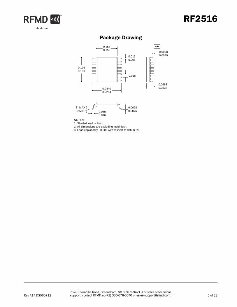
Package Drawing
0.1570.150
0.1960.189
0.24400.2284
0.06880.0532
0.0500.016
0.00980.0075
8° MAX0°MIN
NOTES:1. Shaded lead is Pin 1.2. All dimensions are excluding mold flash.3. Lead coplanarity - 0.005 with respect to datum "A".
0.0120.008
0.025
-A-
0.00980.0040

6 of 22
RF2516
Rev A17 DS0607127628 Thorndike Road, Greensboro, NC 27409-9421 · For sales or technical support, contact RFMD at (+1) 336-678-5570 or [email protected].
RF2516 Theory of Operation
IntroductionShort range radio devices are becoming commonplace in today’s environment. The most common examples are the remotekeyless entry systems popular on many new cars and trucks, and the ubiquitous garage door opener. Other applications areemerging with the growth in home security, automation and the advent of various remote control applications. Typically thesedevices have been simplex, or one-way, links. They are also typically built using surface acoustic wave (SAW) devices as the fre-quency control elements. This approach has been attractive because the SAW devices have been readily available and a trans-mitter, for example, could be built with only a few additional components. Recently however, RF Micro Devices, Inc. (RFMD), hasintroduced several new components that enable a new class of short-range radio devices based on the use of crystals andphase-locked loops for frequency control. These devices are superior in performance and comparable in cost to the traditionalSAW-based designs. The RF2516 is an example of such a device. The RF2516 is targeted for applications such as 315MHzand 433MHz band remote keyless entry systems and wireless security systems, as well as other remote control applications.
The RF2516 TransmitterThe RF2516 is a low-cost AM/ASK VHF/UHF transmitter designed for applications operating within the frequency range of100MHz to 500MHz. In particular, it is intended for 315MHz to 433MHz band systems, remote keyless entry systems, andFCC Part 15.231 periodic transmitters. It can also be used as a local oscillator signal source. The integrated VCO, phase detec-tor, prescaler, and reference oscillator require only the addition of an external crystal to provide a complete phase-locked loop.In addition to the standard power-down mode, the chip also includes an automatic lock-detect feature that disables the trans-mitter output when the PLL is out-of-lock.
The device is manufactured on a 25GHz Silicon Bipolar-CMOS process and packaged in an industry standard SSOP-16 plasticpackage. This, combined with the low external parts count, enables the designer to achieve small-footprint, high-performance,low-cost designs.
The RF2516 is designed to operate from a supply voltage ranging from 2.25V to 3.6V, accommodating designs using threeNiCd battery cells, two AAA flashlight cells, or a lithium button battery. The device is capable of providing up to +10dBm outputpower into a 50Ω load, and is intended to comply with FCC requirements for unlicensed remote control transmitters. ESD pro-tection is provided on all pins except VCO and TX OUT.
While this device is intended for OOK operation, it is possible to use narrowband FM. This is accomplished by modulating thereference oscillator rather than applying the data to the MOD IN input pin. The MOD IN pin should be tied high to cause thedevice to transmit. The deviation will be set by pulling limits of the crystal. Deviation sufficient for the transmission of voice andother low data rate signals can therefore be accomplished. Refer to the Application Schematic in the data sheet for details.
The RF2516 Functional BlocksA PLL consists of a reference oscillator, a phase detector, a loop filter, a voltage controlled oscillator (VCO), and a programma-ble divider in the feedback path. The RF2516 includes all of these internally, except for the loop filter and the reference oscilla-tor’s crystal and two feedback capacitors.
The reference oscillator is a Colpitts type oscillator. Pins 1 (OSC B) and 2 (OSC E) provide connections to a transistor that isused as the reference oscillator. The Colpitts configuration is a low parts count topology with reliable performance and reason-able phase noise. Alternatively, an external signal could be injected into the base of the transistor. The drive level should, ineither case, be around 500mVPP. This level prevents overdriving the device and keeps the phase noise and reference spurs toa minimum.
The prescaler divides the VCO frequency by either 64 or 32, using a series of flip-flops, depending upon the logic level presentat the DIV CTRL pin. A high logic level will select the 64 divisor. A low logic level will select the 32 divisor. This divided signal isthen fed into the phase detector where it is compared with the reference frequency.

7 of 22
RF2516
Rev A17 DS0607127628 Thorndike Road, Greensboro, NC 27409-9421 · For sales or technical support, contact RFMD at (+1) 336-678-5570 or [email protected].
The RF2516 contains an onboard phase detector and charge pump. The phase detector compares the phase of the referenceoscillator to the phase of the VCO. The phase detector is implemented using flip-flops in a topology referred to as either “digitalphase/frequency detector” or “digital tri-state comparator”. The circuit consists of two D flip-flops whose outputs are combinedwith a NAND gate which is then tied to the reset on each flip-flop. The outputs of the flip-flops are also connected to the chargepump. Each flip-flop output signal is a series of pulses whose frequency is related to the flip-flop input frequency.
When both inputs of the flip-flops are identical, the signals are both frequency- and phase-locked. If they are different, they willprovide signals to the charge pump which will either charge or discharge the loop filter, or enter into a high impedance state.The name “tri-state comparator” comes from this.
The main benefit of this type of detector is the ability to correct for errors in both phase and frequency. When locked, the detec-tor uses phase error for correction. When unlocked, it uses frequency error for correction. This type of detector will lock underall conditions.
The charge pump consists of two transistors, one for charging the loop filter and the other for discharging the loop filter. Itsinputs are the outputs of the phase detector flip-flops. Since there are two flip-flops, there are four possible states. If bothamplifier inputs are low, then the amplifier pair goes into a high impedance state, maintaining the charge on the loop filter. Thestate where both inputs are high will not occur. The other states are either charging or discharging the loop filter. The loop filterintegrates the pulses coming from the charge pump to create a control voltage for the voltage controlled oscillator.
The VCO is a tuned differential amplifier with the bases and collectors cross-coupled to provide positive feedback and a 360°phase shift. The tuned circuit is located in the collectors, and is comprised of internal varactors and external inductors. Thedesigner selects the inductors for the desired frequency of operation. These inductors also provide DC bias for the VCO.
The output of the VCO is buffered and applied to the prescaler circuit, where it is divided by either 32 or 64, as selected by thedesigner, and compared to the reference oscillator frequency.
The transmit amplifier is a two-stage amplifier consisting of a driver and an open collector final stage. It is capable of providing10dBm of output power into a 50Ω load while operating from a 3.6V power supply.
The lock-detect circuitry connects to the output of the phase detector circuitry and is used to disable the transmitter when theVCO is not phase-locked to the reference oscillator. This is necessary to avoid unwanted out-of-band transmission and to pro-vide compliance with regulatory limits during an unlocked condition.
There are many possible reasons for the PLL not to be locked. For instance, there is a short period during the start of any VCOin which the VCO begins oscillating and the reference oscillator builds up to full amplitude. During this period, the frequencywill likely be outside the authorized band. Typically, the VCO starts much faster than the reference oscillator. Once both VCOand reference oscillators are running, the phase detector can start slewing the VCO to the correct frequency, slowly slidingacross 200MHz of occupied spectrum. In competitive devices, the VCO radiates at full power under all of these conditions.
The lock protection circuit in the RF2516 is intended to stabilize quickly after power is applied to the chip, and to disable thebase drive to the transmit amplifier. This attenuates the output to levels that will be generally acceptable to regulatory boardsas spurious emissions. Once the phase detector has locked the oscillators, then the lock circuit enables the MOD IN pin fortransmission of the desired data. There is no need for an external microprocessor to monitor the lock status, although that canbe done with a low current A/D converter in a system micro, if needed. The lock-detect circuitry contains an internal resistorwhich, combined with a designer-chosen capacitor for a particular RC time constant, filters the lock-detect signal. This signal isthen passed through an internal Schmitt trigger and used to enable or disable the transmit amplifier.
If the oscillator unlocks, even momentarily, the protection circuit quickly disables the output until the lock is stable. Theseunlocks can be caused by low battery voltage, poor power supply regulation, severe shock of the crystal or VCO, antenna load-ing, component failure, or a myriad of unexpected single-point failures.
The RF2516 contains onboard band gap reference voltage circuitry which provides a stable DC bias over varying temperatureand supply voltages. Additionally, the device features a power-down mode, eliminating battery disconnect switches.

8 of 22
RF2516
Rev A17 DS0607127628 Thorndike Road, Greensboro, NC 27409-9421 · For sales or technical support, contact RFMD at (+1) 336-678-5570 or [email protected].
Designing With the RF2516The reference oscillator is built around the onboard transistor at pins 1 and 2. The intended topology is that of a Colpitts oscil-lator. The Colpitts oscillator is quite common and requires few external components, making it ideal for low-cost solutions. Thetopology of this type of oscillator is as seen in the following figure.
This type of oscillator is a parallel resonant circuit for a fundamental mode crystal. The transistor amplifier is an emitter fol-lower and the voltage gain is developed by the tapped capacitor impedance transformer. The series combination of C1 and C2
act in parallel with the input capacitance of the transistor to capacitively load the crystal.
The nominal capacitor values can be calculated with the following equations6:
and
The load capacitance is usually 32pF. The variable freq is the oscillator frequency in MHz. The frequency can be adjusted byeither changing C2 or by placing a variable capacitor in series with the crystal. As an example, assume a desired frequency of14MHz and a load capacitance of 32pF. C1=137.1pF and C2=41.7pF.
These capacitor values provide a starting point. The drive level of the oscillator should be checked by looking at the signal atpin 2 (OSC E). It has been found that the level at this pin should generally be around 500mVPP or less. This will reduce the ref-erence spur levels and reduce noise from distortion. If this level is higher than 500mVPP then increase the value of C1. The val-ues of these capacitors are usually tweaked during design to meet performance goals, such as minimizing the start-up time.
Additionally, by placing a variable capacitor in series with the crystal, one is able to adjust the frequency. This will also alter thedrive level, so it should be checked again.
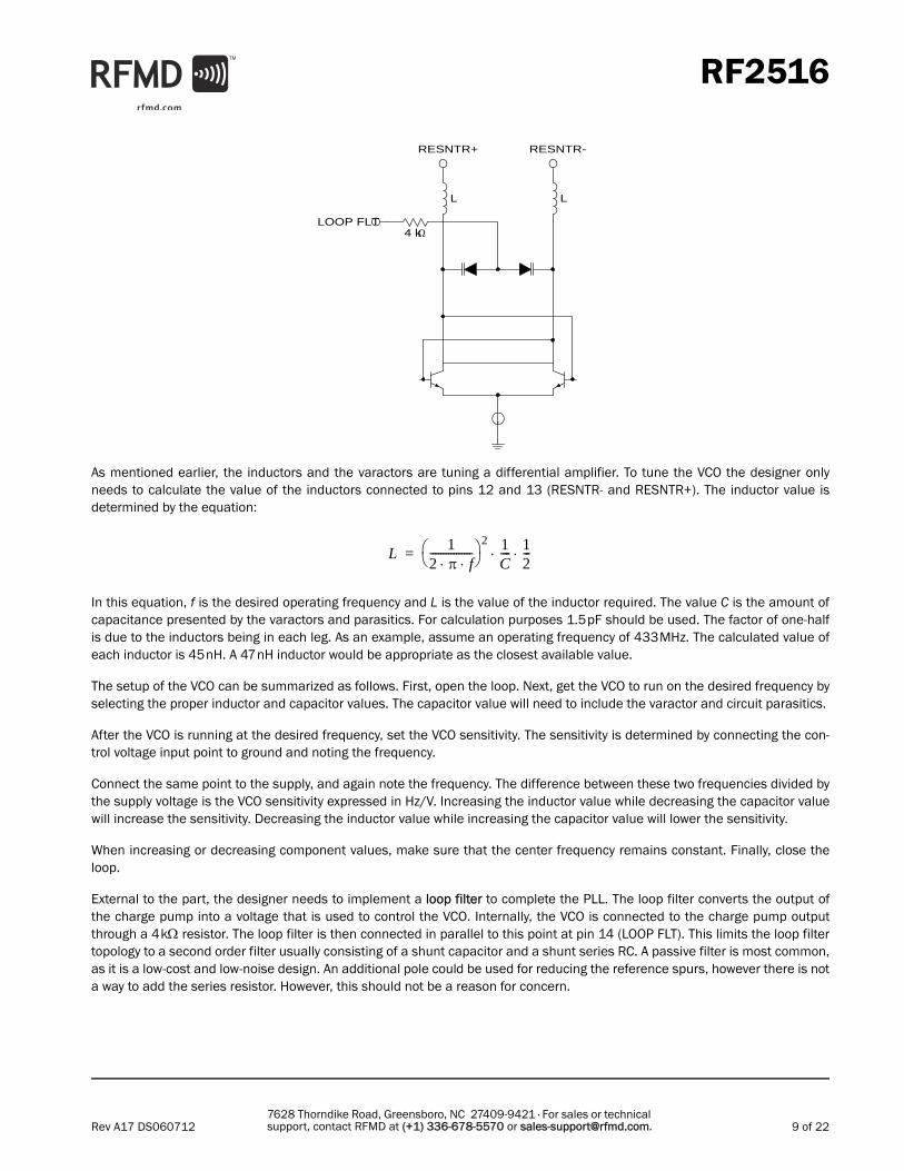
An important part of the overall design is the voltage controlled oscillator. The VCO is configured as a differential amplifier. TheVCO is tuned via internal varactors. The varactors are tuned by the loop filter output voltage through a 4kΩ resistor.
X1 C2
C1
VCC
C160 Cload⋅freqMHz
------------------------= C21
1Cload------------- 1
C1------–
--------------------------=
9 of 22
RF2516
Rev A17 DS0607127628 Thorndike Road, Greensboro, NC 27409-9421 · For sales or technical support, contact RFMD at (+1) 336-678-5570 or [email protected].
As mentioned earlier, the inductors and the varactors are tuning a differential amplifier. To tune the VCO the designer onlyneeds to calculate the value of the inductors connected to pins 12 and 13 (RESNTR- and RESNTR+). The inductor value isdetermined by the equation:
In this equation, f is the desired operating frequency and L is the value of the inductor required. The value C is the amount ofcapacitance presented by the varactors and parasitics. For calculation purposes 1.5pF should be used. The factor of one-halfis due to the inductors being in each leg. As an example, assume an operating frequency of 433MHz. The calculated value ofeach inductor is 45nH. A 47nH inductor would be appropriate as the closest available value.
The setup of the VCO can be summarized as follows. First, open the loop. Next, get the VCO to run on the desired frequency byselecting the proper inductor and capacitor values. The capacitor value will need to include the varactor and circuit parasitics.
After the VCO is running at the desired frequency, set the VCO sensitivity. The sensitivity is determined by connecting the con-trol voltage input point to ground and noting the frequency.
Connect the same point to the supply, and again note the frequency. The difference between these two frequencies divided bythe supply voltage is the VCO sensitivity expressed in Hz/V. Increasing the inductor value while decreasing the capacitor valuewill increase the sensitivity. Decreasing the inductor value while increasing the capacitor value will lower the sensitivity.
When increasing or decreasing component values, make sure that the center frequency remains constant. Finally, close theloop.
External to the part, the designer needs to implement a loop filter to complete the PLL. The loop filter converts the output ofthe charge pump into a voltage that is used to control the VCO. Internally, the VCO is connected to the charge pump outputthrough a 4kΩ resistor. The loop filter is then connected in parallel to this point at pin 14 (LOOP FLT). This limits the loop filtertopology to a second order filter usually consisting of a shunt capacitor and a shunt series RC. A passive filter is most common,as it is a low-cost and low-noise design. An additional pole could be used for reducing the reference spurs, however there is nota way to add the series resistor. However, this should not be a reason for concern.
4 kΩLOOP FLT
L L
RESNTR+ RESNTR-
L 12 π f⋅ ⋅----------------⎝ ⎠
⎛ ⎞ 2 1C---- 1
2---⋅ ⋅=

10 of 22
RF2516
Rev A17 DS0607127628 Thorndike Road, Greensboro, NC 27409-9421 · For sales or technical support, contact RFMD at (+1) 336-678-5570 or [email protected].
The schematic of the loop filter is:
The transfer function is:
where the time constants are defined as:
and
The frequency at which unity gain occurs is given by:
This is also the loop bandwidth.
If the phase margin (PM) and the loop bandwidth (ωLBW) are known, it is possible to calculate the time constants. These are
found using the equations4:
and
4 kΩLOOP FLT
L L
RESNTR+ RESNTR-
F s( ) R2s τ2 1+⋅
s τ2 s τ1 1 )+⋅(⋅ ⋅-------------------------------------------⋅=
τ2 R2 C2⋅= τ1 R2C1 C2⋅C1 C2+-------------------⎠
⎞⎝⎛⋅=
ωLBW1
τ1 τ2⋅-------------------=
τ1PM( )sec PM( )tan–
ωLBW--------------------------------------------------= τ2
1ωLBW
2 τ1⋅------------------------=

11 of 22
RF2516
Rev A17 DS0607127628 Thorndike Road, Greensboro, NC 27409-9421 · For sales or technical support, contact RFMD at (+1) 336-678-5570 or [email protected].
With these known, it is then possible to determine the values of the filter components.4
As an example, consider a loop bandwidth of 50kHz, a phase margin of 45°, a divide ratio of 64, a KVCO of 20MHz/V, and aKPD of 100μA/2πrad. Time constant τ1 is 1.31848μs, time constant τ2 is 7.68468μs, C1 is 20.9pF, C2 is 100.8pF, and R2 is76.2kΩ.
In order to perform these calculations, one will need to know the value of two constants, KVCO and KPD. KPD is calculated bydividing the charge pump current by 2π. For the RF2516, the charge pump current is 100μA. KVCO is best found empirically asit will change with frequency and board parasitics. By briefly connecting pin 14 (LOOP FLT) to VCC and then to ground, the fre-quency tuning range of the VCO can be seen. Dividing the difference between these two frequencies by the difference in thevoltage gives KVCO in MHz/V.
The control lines provide an interface for connecting the device to a microcontroller or other signal generating mechanism. Thedesigner can treat pin 8 (MOD IN), pin 16 (DIV CTRL), and pin 3 (PD) as control pins whose voltage level can be set. The lock-detect voltage at pin 15 (LD FLT) is an output that can be monitored by the microcontroller.
Pin 15 (LD FLT) is used to set the threshold of the lock-detect circuit. A shunt capacitor is used to set an RC time constant withan on-chip series 1kΩ resistor. The time constant should be approximately 10 times the reference period.
General RF bypassing techniques must be observed to get the best performance. Choose capacitors such that they are seriesresonant near the frequency of operation.
Board layout is always an area in which great care must be taken. The board material and thickness are used in calculating theRF line widths. The use of vias for connection to the ground plane allows one to connect to ground as close as possible toground pins. When laying out the traces around the VCO, it is desirable to keep the parasitics equal between the two legs. Thiswill allow equal valued inductors to be used.
Pre-compliance testing should be performed during the design process. This can be done with a GTEM cell or at a compliancetesting laboratory. It is recommended that pre-compliance testing be performed so that there are no surprises during finalcompliance testing. This will help keep the product development and release on schedule.
Working with a laboratory offers the benefit of years of compliance testing experience and familiarity with the regulatoryissues. Also, the laboratory can often provide feedback that will help the designer make the product compliant.
On the other hand, having a GTEM cell or an open air test site locally offers the designer the ability to rapidly determinewhether or not design changes impact the product's compliance. Set-up of an open air test site and the associated calibrationis not trivial. An alternative is to use a GTEM test cell.
After the design has been completed and passes compliance testing, application will need to be made with the respective reg-ulatory bodies for the geographic region in which the product will be operated to obtain final certifications.
C1τ1τ2-----
KPD KVCO⋅
ωLBW2 N⋅
-----------------------------1 ωLBW τ2⋅( )2+
1 ωLBW τ1⋅( )2+----------------------------------------⋅ ⋅=
C2 C1τ2τ1----- 1–⎝ ⎠
⎛ ⎞⋅= R2τ2C2------=

12 of 22
RF2516
Rev A17 DS0607127628 Thorndike Road, Greensboro, NC 27409-9421 · For sales or technical support, contact RFMD at (+1) 336-678-5570 or [email protected].
RF2516 Typical ApplicationsFCC Part 15.231 Periodic Transmitter - 315MHz Automotive Keyless Entry Transmitter
The following information is taken or paraphrased from the Code of Federal Regulations Title 47, Part 15, Section 231 (47 CFR15.231). Part 15 discusses radio frequency devices and section 231 discusses periodic transmissions. Please refer to the reg-ulation itself as the final authority. Additional information may be found on the Internet at www.fcc.gov.
To highlight the main guidelines outlined by this section, there are five main limitations: operating frequency, transmission con-tent, transmission duration, emission bandwidth, and spurious emissions.
Part 15.231 allows operation in two bands: 40.66MHz to 40.70MHz and above 70MHz. Transmission is limited to control sig-nals such as alarm systems, door openers, remote switches, etc. Radio control of toys is not permitted, nor is continuous trans-mission such as voice or video. Data transmission other than a recognition code is not permitted. Transmission time is limitedto 5 seconds (paragraph a) or for 1 second with greater than ten seconds off (paragraph e).
Emission bandwidth between 70MHz and 900MHz can not be more than 0.25% of the center frequency. Above 900MHz, theemission bandwidth cannot be greater than 0.50% of the center frequency. The emission bandwidth is determined from thepoints that are 20dB down from the modulated carrier. This corresponds to an occupied bandwidth of 4.5MHz at a center fre-quency of 902MHz, 1.1MHz at 433MHz, and 788kHz at 315MHz.
Spurious emissions limits are listed in tabular form for various frequency ranges in the Section 231. Above 470MHz with amanually activated transmitter, the fundamental field strength at a distance of 3 meters shall not exceed12,500microvolts/meter. The spurious emissions shall not exceed 1,250microvolt/meter at a distance of 3meters above470MHz. Refer to Appendix A for a method of converting field strength to power.
In the frequency range of 260MHz to 470MHz, one needs to linearly interpolate the maximum emissions level for both the fun-damental and spurious emissions. The equation for this line is given by:
This equation is derived from the endpoints of the frequency range and their respective field strengths. Note that the fieldstrength is in microvolts per meter and the frequency is in megahertz. To determine the spurious level, divide the level calcu-lated above for the spurious frequency by ten.
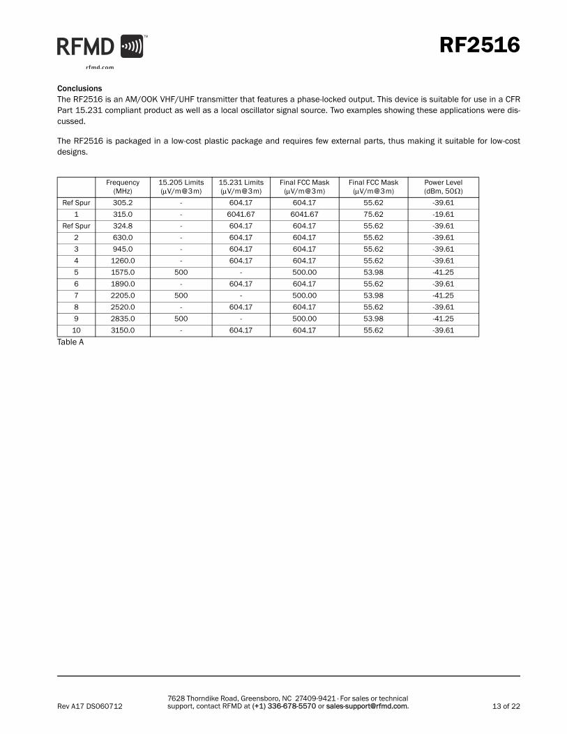
As an example, assume the fundamental is 315MHz and the reference frequency is 9.8MHz. The field strengths of the funda-mental, the reference spurs, and the harmonics of the fundamental up through the tenth harmonic are calculated in the follow-ing table The occupied bandwidth limit is 787.5kHz. As shown in Table A, the fifth, seventh, and ninth harmonics fall intorestricted bands as called out in section 15.205. The limits for these restricted bands are called out in section 15.209. Thepower level in the last column is the level if the output is connected directly to a spectrum analyzer. Refer to Appendix A as tohow this column was calculated.
Local Oscillator SourceSince the RF2516 has a phase-locked VCO, it can be used as a signal source. The device is an ASK/OOK transmitter, with thedata provided at the MOD IN pin. When the MOD IN is a high logic level, the carrier is transmitted. When MOD IN is a low logiclevel, then the carrier is not transmitted. Therefore, to use the RF2516 as signal source, simply tie the MOD IN pin to the supplyvoltage, through a suitable series resistor (minimum 3kΩ).
EμVm-------
4123--- FreqMHz 70831
3---–⋅=
13 of 22
RF2516
Rev A17 DS0607127628 Thorndike Road, Greensboro, NC 27409-9421 · For sales or technical support, contact RFMD at (+1) 336-678-5570 or [email protected].
ConclusionsThe RF2516 is an AM/OOK VHF/UHF transmitter that features a phase-locked output. This device is suitable for use in a CFRPart 15.231 compliant product as well as a local oscillator signal source. Two examples showing these applications were dis-cussed.
The RF2516 is packaged in a low-cost plastic package and requires few external parts, thus making it suitable for low-costdesigns.
Table A
Frequency(MHz)
15.205 Limits(μV/m@3m)
15.231 Limits(μV/m@3m)
Final FCC Mask(μV/m@3m)
Final FCC Mask(μV/m@3m)
Power Level(dBm, 50Ω)
Ref Spur 305.2 - 604.17 604.17 55.62 -39.61
1 315.0 - 6041.67 6041.67 75.62 -19.61
Ref Spur 324.8 - 604.17 604.17 55.62 -39.61
2 630.0 - 604.17 604.17 55.62 -39.61
3 945.0 - 604.17 604.17 55.62 -39.61
4 1260.0 - 604.17 604.17 55.62 -39.61
5 1575.0 500 - 500.00 53.98 -41.25
6 1890.0 - 604.17 604.17 55.62 -39.61
7 2205.0 500 - 500.00 53.98 -41.25
8 2520.0 - 604.17 604.17 55.62 -39.61
9 2835.0 500 - 500.00 53.98 -41.25
10 3150.0 - 604.17 604.17 55.62 -39.61

14 of 22
RF2516
Rev A17 DS0607127628 Thorndike Road, Greensboro, NC 27409-9421 · For sales or technical support, contact RFMD at (+1) 336-678-5570 or [email protected].
Pin Out
1
2
3
4
5
6
7
8
16
15
14
13
12
11
10
9
DIV CTRL
LD FLT
LOOP FLT
RESNTR+
RESNTR-
VREFP
GND2
VCC2
OSC B
OSC E
PD
GND
TX OUT
GND1
VCC1
MOD IN

15 of 22
RF2516
Rev A17 DS0607127628 Thorndike Road, Greensboro, NC 27409-9421 · For sales or technical support, contact RFMD at (+1) 336-678-5570 or [email protected].
Application Schematic315MHz
1
2
3
4
5
6
7
8
16
15
14
13
12
11
10
9
68 pF
9.83 MHz
33pF
*Not populated on standard Evaluation Board.
OSC B
OSC E
GND
TX OUT
GND1
VCC1
MOD IN
DIV CTRL
LD FLT
LOOP FLT
RESNTR+
RESNTR-
VREFP
GND2
VCC2
50 Ω μstrip4 pF50 Ω μstrip
56 nH
16 kΩ
J1TX OUT
220 pF
10 ΩTX VCC
100 pF
MOD IN
S1
CAS-120B
10 Ω
82 nH
82 nH2 kΩ
10 nF
4.3 kΩ 2.2 nF
1 nF
VC
C
VC
C
VC
C
PD

16 of 22
RF2516
Rev A17 DS0607127628 Thorndike Road, Greensboro, NC 27409-9421 · For sales or technical support, contact RFMD at (+1) 336-678-5570 or [email protected].
Application Schematic315MHz
1
2
3
4
5
6
7
8
16
15
14
13
12
11
10
9
68 pF
9.83 MHz
33pF
OSC B
OSC E
GND
TX OUT
GND1
VCC1
MOD IN
DIV CTRL
LD FLT
LOOP FLT
RESNTR+
RESNTR-
VREFP
GND2
VCC2
50 Ω μstrip4 pF50 Ω μstrip
56 nH
16 kΩ
J1TX OUT
220 pF
10 ΩTX VCC
100 pF
S1
CAS-120B
10 Ω
82 nH
82 nH2 kΩ
10 nF
4.3 kΩ 2.2 nF
1 nF
PD
D1SMV1249-011
150 kΩAUDIO
VCC
VCC
RF2516 Audio Transmitter
VCC
VCC

17 of 22
RF2516
Rev A17 DS0607127628 Thorndike Road, Greensboro, NC 27409-9421 · For sales or technical support, contact RFMD at (+1) 336-678-5570 or [email protected].
Application Schematic433MHz
1
2
3
4
5
6
7
8
16
15
14
13
12
11
10
9
68 pF
13.57734 MHz
PWR DWN4.3 kΩ
220 pF
220 pF 10 nF
220 pF
DIV CTR
10 nF
TX OUT
33pF
1 nF
2.2 nF
39 nH
2 kΩ10 Ω
10 nF
*Not populated on standard Evaluation Board.
*
2.8
VCC (V) Mod. in Res. Value(R5)
ICC(mA)
POUT(dBm)
1k3k5k7k9k11k13k15k17k19k21k
17.3810.518.687.827.186.756.456.185.995.805.66
7.458.787.236.004.733.812.982.301.631.000.35
2.0
VCC (V) Mod. in Res. Value(R5)1k3k5k7k9k11k13k15k17k19k21k
ICC(mA)11.0810.834.614.003.633.423.263.153.073.012.95
POUT(dBm)-6.23-4.40-5.61-6.66-8.08-8.93-10.04-10.71-11.58-12.32-13.10
2.4
VCC (V) Mod. in Res. Value(R5)1k3k5k7k9k11k13k15k17k19k21k
ICC(mA)14.059.007.486.736.165.795.535.295.134.984.86
POUT(dBm)7.947.635.954.643.352.401.470.750.05-0.60-1.26
3.2
VCC (V) Mod. in Res. Value(R5)1k3k5k7k9k11k13k15k17k19k21k
POUT(dBm)6.779.708.307.115.915.024.163.512.892.261.66
ICC(mA)20.9012.129.668.958.237.757.427.106.896.686.52
3.6
VCC (V) Mod. in Res. Value(R5)1k3k5k7k9k11k13k15k17k19k21k
POUT(dBm)5.7810.429.188.086.886.025.194.523.933.352.72
ICC(mA)24.6813.8810.9410.149.348.818.448.097.867.637.44
OSC B
OSC E
GND
TX OUT
GND1
VCC1
MOD IN
DIV CTRL
LD FLT
LOOP FLT
RESNTR+
RESNTR-
VREFP
GND2
VCC2
50 Ω μstrip4 pF50 Ω μstrip68 nH2 pF50 Ω μstrip
15 pF 10 nH 15 pF10 nH
22 nH
220 pF10 nF
220 pF10 nF10 Ω
3 kΩ 10 nF
MOD IN
39 nH
VCC
VCC
VCC
PD

18 of 22
RF2516
Rev A17 DS0607127628 Thorndike Road, Greensboro, NC 27409-9421 · For sales or technical support, contact RFMD at (+1) 336-678-5570 or [email protected].
Evaluation Board Schematic315MHz
1
2
3
4
5
6
7
8
16
15
14
13
12
11
10
9
C868 pF
Y19.83 MHz
C733pF
*Not populated on standard Evaluation Board.
OSC B
OSC E
GND
TX OUT
GND1
VCC1
MOD IN
DIV CTRL
LD FLT
LOOP FLT
RESNTR+
RESNTR-
VREFP
GND2
VCC2
50 Ω μstrip
C64 pF50 Ω μstrip
L356 nH
R416 kΩ
J1TX OUT
C5220 pF
TX VCC
C4100 pF
MOD IN
S1
CAS-120B
R210 Ω
L282 nH
L182 nH
R12 kΩ
C11 μF
R34.3 kΩ
C22.2 nF
C31 nF
VCC
VCC
VCC
GND
P1-1 VCC1
P1-3 MOD IN
P1
1
2
3
CON3B1
LITH BATT
VCC
+
-
2516400, rev A
PD
R510 Ω

19 of 22
RF2516
Rev A17 DS0607127628 Thorndike Road, Greensboro, NC 27409-9421 · For sales or technical support, contact RFMD at (+1) 336-678-5570 or [email protected].
Evaluation Board Schematic433MHz
1
2
3
4
5
6
7
8
16
15
14
13
12
11
10
9
C268 pF
X113.57734 MHz
PWR DWN
R24.3k Ω
C7220 pF
C9220 pF
C1010 nF
VCC
C12220 pF
DIV CTRL
C1110 nF
C133pF
C61 nF
C82.2 nF
L239 nH
R42k Ω
R310 Ω
C1310 nF
*Not populated on standard Evaluation Board.
C17*OSC B
OSC E
GND
TX OUT
GND1
VCC1
MOD IN
DIV CTRL
LD FLT
LOOP FLT
RESNTR+
RESNTR-
VREFP
GND2
VCC2
50 Ω μstrip
C34 pF50 Ω μstrip
L468 nH
C152 pF50 Ω μstrip
C1415 pF
L310 nH
C1615 pF
L510 nH
L622 nH
C18220 pF
C1910 nF
VCC
C5220 pF
C410 nF
R110 Ω
VCC
R53k Ω
C2010 nF
L139 nHJ1
TX OUT
J2MOD IN
P1
1
2
3
CON3
VCC
NC
GND
P2
1
2
3
CON3
DIV CTRL
GND
PWR DWN
PD

20 of 22
RF2516
Rev A17 DS0607127628 Thorndike Road, Greensboro, NC 27409-9421 · For sales or technical support, contact RFMD at (+1) 336-678-5570 or [email protected].
Evaluation Board Layout (315MHz)Board Size 1.285” x 1.018”
Board Thickness 0.062”, Board Material FR-4

21 of 22
RF2516
Rev A17 DS0607127628 Thorndike Road, Greensboro, NC 27409-9421 · For sales or technical support, contact RFMD at (+1) 336-678-5570 or [email protected].
Evaluation Board Layout (433MHz)Board Size 1.392” x 0.813”
Board Thickness 0.062”, Board Material FR-4

22 of 22
RF2516
Rev A17 DS0607127628 Thorndike Road, Greensboro, NC 27409-9421 · For sales or technical support, contact RFMD at (+1) 336-678-5570 or [email protected].
433MHz Phase Noise
0 1.0
1.0
-1.0
10.0
10.0
-10.0
5.0
5.0
-5.02.
0
2.0
-2.0
3.0
3.0
-3.0
4.0
4.0
-4.0
0.2
0.2
-0.2
0.4
0.4
-0.4
0.6
0.6
-0.6
0.8
0.8
-0.8
RF2516 Output ZSwp Max
1GHz
Swp Min0.1GHz
VCC = 3 V
VCC = 2 V
VCC = 3.3 V
1.0 GHz 0.1 GHz