Embed Size (px)
Citation preview
1SLAU603B–December 2014–Revised June 2017Submit Documentation Feedback
Copyright © 2014–2017, Texas Instruments Incorporated
RF430FRL15xH Firmware User's Guide
User's GuideSLAU603B–December 2014–Revised June 2017
RF430FRL15xH Firmware User's Guide
The Texas Instruments RF430FRL15xH is a 13.56-MHz transponder chip with a programmable 16-bitMSP430™ low-power microcontroller. This document describes the operation of ROM firmware for theRF430FRL15xH ISO/IEC 15693 sensor transponder. This device contains firmware that exists in ROMand allows the sampling from several analog sources and storage. All sources are controlled throughmemory-mapped registers existing in FRAM. The sensors can include a thermistor and several otheranalog sources including an internal on-die temperature sensor and a digital sensor that is connectedthrough an I2C or SPI bus. The ROM firmware control and status blocks are located in FRAM. Issuingcommands, controlling, and reading of stored data from the device can be done through theISO/IEC 15693 RF interface or through an optional host controller, if an external I2C- or SPI-based sensoris not used.
Contents1 RF430FRL15xH Overview.................................................................................................. 3
1.1 Operation Modes of RF430FRL15xH ............................................................................ 31.2 Default Operation ................................................................................................... 31.3 ROM Sensor Support Disabled ................................................................................... 31.4 I2C and SPI Disabled ............................................................................................... 4
2 Application Level Description............................................................................................... 42.1 Function Overview .................................................................................................. 42.2 ROM Firmware Flow Overview ................................................................................... 52.3 Powering the Device ............................................................................................... 52.4 Possible Sensors ................................................................................................... 62.5 Sampling Process Configuration Options........................................................................ 62.6 Sensor Configuration ............................................................................................... 72.7 Thermistor ........................................................................................................... 92.8 Determining the Voltage From the Raw ADC Value ........................................................... 92.9 Storage of Sampling Data........................................................................................ 102.10 Data Transfer ...................................................................................................... 102.11 FRAM Memory Map............................................................................................... 112.12 Errors ............................................................................................................... 11
3 Sensor Sampling Scheduler .............................................................................................. 123.1 Examples ........................................................................................................... 12
4 RF Stack..................................................................................................................... 144.1 Summary ........................................................................................................... 144.2 Supported Commands............................................................................................ 144.3 Supported Configurations ........................................................................................ 154.4 Memory Use ....................................................................................................... 154.5 ISO/IEC 15693 Memory Map .................................................................................... 164.6 ISO/IEC 15693 Lock Block Commands Behavior............................................................. 164.7 Custom Commands ............................................................................................... 174.8 Custom Read Single With 16-Bit Block Number .............................................................. 174.9 Custom Write Single With 16-Bit Block Number .............................................................. 174.10 Custom Lock Block With 16-Bit Block Number................................................................ 184.11 Custom Read Multiple With 16-Bit Block Number ............................................................ 184.12 Custom Write Multiple With 16-Bit Block Number ............................................................ 184.13 Limitations .......................................................................................................... 194.14 RF Stack Memory Access Protection........................................................................... 19
www.ti.com
2 SLAU603B–December 2014–Revised June 2017Submit Documentation Feedback
Copyright © 2014–2017, Texas Instruments Incorporated
RF430FRL15xH Firmware User's Guide
5 Interfacing a Host Controller .............................................................................................. 195.1 Host Controller..................................................................................................... 195.2 I2C and SPI Host Controller Communication Protocol........................................................ 195.3 I2C Host Controller Communication Protocol .................................................................. 205.4 SPI Protocol........................................................................................................ 235.5 Host Controller Memory Access Range ........................................................................ 265.6 Interrupts ........................................................................................................... 27
6 Example Projects........................................................................................................... 286.1 Blank Project ....................................................................................................... 286.2 ISO/IEC 15693 RF Stack (NFC) Only .......................................................................... 286.3 External Digital Sensor Driver Firmware (Sensor Hub BoosterPack) ...................................... 28
7 Registers .................................................................................................................... 317.1 Reading the Register Address Bar.............................................................................. 317.2 Firmware General Control Register............................................................................. 327.3 Firmware Status Register ........................................................................................ 337.4 Sensor Control Register .......................................................................................... 347.5 Frequency Register ............................................................................................... 347.6 Number of Passes Register...................................................................................... 357.7 Averaging Register................................................................................................ 357.8 Interrupt Control Register ........................................................................................ 367.9 Error Control Register ............................................................................................ 377.10 Reference-ADC1 Sensor Skip Count Register ................................................................ 387.11 Thermistor-ADC2 Sensor Skip Count Register................................................................ 387.12 ADC0 Sensor Skip Count Register ............................................................................. 387.13 Internal Sensor Skip Count Register............................................................................ 397.14 Digital Sensor 1 Skip Count Register........................................................................... 397.15 Digital Sensor 2 Skip Count Register........................................................................... 397.16 Digital Sensor 3 Skip Count Register........................................................................... 407.17 Number of Blocks Received Register .......................................................................... 407.18 Reference-ADC1 Configuration Register....................................................................... 417.19 Thermistor-ADC2 Sensor Configuration Register............................................................. 427.20 ADC0 Sensor Configuration Register........................................................................... 437.21 Internal Sensor Configuration Register......................................................................... 447.22 Initial Delay Period Setup Register ............................................................................. 447.23 JTAG Enable Password Register ............................................................................... 457.24 Initial Delay Period Register ..................................................................................... 457.25 Custom Timer Value Register ................................................................................... 457.26 Low Threshold Reference-ADC1 Register ..................................................................... 467.27 High Threshold Reference-ADC1 Register .................................................................... 467.28 Low Threshold Thermistor-ADC2 Sensor Register ........................................................... 467.29 High Threshold Thermistor-ADC2 Sensor Register .......................................................... 477.30 Low Threshold ADC0 Sensor Register ......................................................................... 477.31 High Threshold ADC0 Sensor Register ........................................................................ 477.32 Low Threshold Internal Temperature Sensor Register....................................................... 487.33 High Threshold Internal Temperature Sensor Register ...................................................... 487.34 Low Threshold Digital1 Sensor Register ....................................................................... 497.35 High Threshold Digital1 Sensor Register ...................................................................... 497.36 Low Threshold Digital2 Sensor Register ....................................................................... 497.37 High Threshold Digital2 Sensor Register ...................................................................... 507.38 Low Threshold Digital3 Sensor Register ....................................................................... 507.39 High Threshold Digital3 Sensor Register ...................................................................... 507.40 Reference or ADC1 Alarm Configuration Register............................................................ 517.41 Thermistor and ADC2 Alarm Configuration Register ......................................................... 517.42 ADC0 Alarm Configuration Register ............................................................................ 527.43 Internal Alarm Configuration Register .......................................................................... 527.44 Digital 1 Alarm Configuration Register ......................................................................... 53

www.ti.com RF430FRL15xH Overview
3SLAU603B–December 2014–Revised June 2017Submit Documentation Feedback
Copyright © 2014–2017, Texas Instruments Incorporated
RF430FRL15xH Firmware User's Guide
7.45 Digital 2 Alarm Configuration Register ......................................................................... 537.46 Digital 3 Alarm Configuration Register ......................................................................... 547.47 Logging Memory Size Register.................................................................................. 547.48 Total Number of Stores Register ................................................................................ 557.49 Last Logged Index Register...................................................................................... 557.50 FRAM Data Valid Register ....................................................................................... 557.51 Logging Memory Space .......................................................................................... 567.52 Firmware Version Register....................................................................................... 567.53 FRAM Access Limit Register .................................................................................... 577.54 Firmware System Control Register ............................................................................. 57
8 Production Programming .................................................................................................. 589 Adding Custom Commands............................................................................................... 58
9.1 Custom Command Format ....................................................................................... 58
TrademarksMSP430 is a trademark of Texas Instruments.All other trademarks are the property of their respective owners.
1 RF430FRL15xH Overview
1.1 Operation Modes of RF430FRL15xHThis user's guide describes the interface and operation of firmware for the RF430FRL15xH. The firmwareexists in ROM and allows analog and digital sampling from several sources. They are a digital sensor thatis connected through an I2C or SPI bus, a possible thermistor, and several other analog sources includingan internal on-die temperature sensor. The data from the sensors is collected and, if selected, averagingis performed before the data is stored to FRAM. The firmware control and status blocks and samplesstorage are located on FRAM. Issuing commands, controlling and reading of stored data from the deviceis done through the ISO/IEC 15693 RF interface or through an optional host controller, if an external I2C orSPI sensor is not used.
NOTE: The RF430FRL154H does not have an SD14 module, thus this section describing the defaultoperation of the firmware does not apply to that device. The RF430FRL154H does supportISO/IEC 15693 and an eUSCI module that can be used.
1.2 Default OperationThis mode is the default mode and, if the device has not been programmed, is the mode that is activated.ROM RF stack is operational on this mode. The FRAM memory map is set to default values. Any writes tothe Firmware General Control register are acted upon. The device waits for further configuration to runsensor sampling and data storage.
In this mode, there is support for the analog sensors, host controller, RF stack, and all other ROMfunctionality.
1.3 ROM Sensor Support DisabledThis mode disables the SD14 ADC functionality. Most of the virtual registers in FRAM are nonfunctional(see Section 7 for which registers are not functional). Writes through RF or host controller to the controlstatus registers do not activate a sampling process. This mode is set using the Firmware System Controlregister (Section 7.54).
The ROM sensor support is disabled in the RF430FRL154H automatically. This same state can beentered in any device variant by the clearing the ROM sensor support enable bit in the Firmware SystemControl register (Section 7.54).
RF430FRL15xH Overview www.ti.com
4 SLAU603B–December 2014–Revised June 2017Submit Documentation Feedback
Copyright © 2014–2017, Texas Instruments Incorporated
RF430FRL15xH Firmware User's Guide
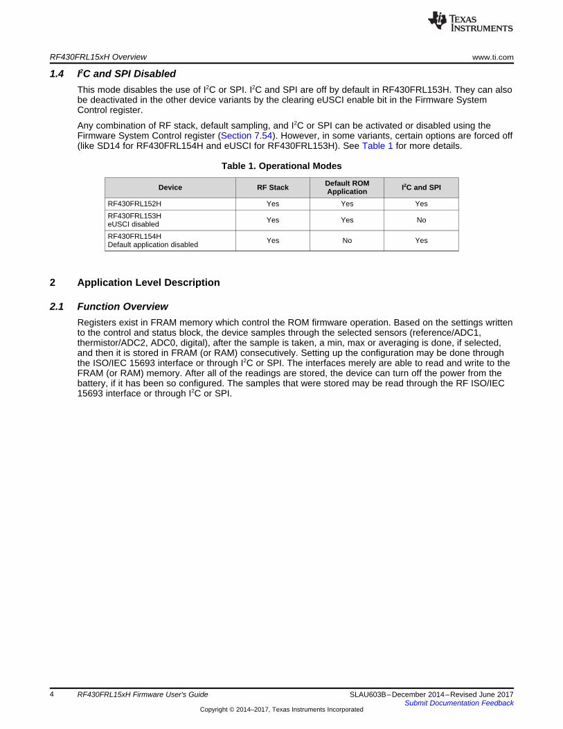
1.4 I2C and SPI DisabledThis mode disables the use of I2C or SPI. I2C and SPI are off by default in RF430FRL153H. They can alsobe deactivated in the other device variants by the clearing eUSCI enable bit in the Firmware SystemControl register.
Any combination of RF stack, default sampling, and I2C or SPI can be activated or disabled using theFirmware System Control register (Section 7.54). However, in some variants, certain options are forced off(like SD14 for RF430FRL154H and eUSCI for RF430FRL153H). See Table 1 for more details.
Table 1. Operational Modes
Device RF Stack Default ROMApplication I2C and SPI
RF430FRL152H Yes Yes YesRF430FRL153HeUSCI disabled Yes Yes No
RF430FRL154HDefault application disabled Yes No Yes
2 Application Level Description
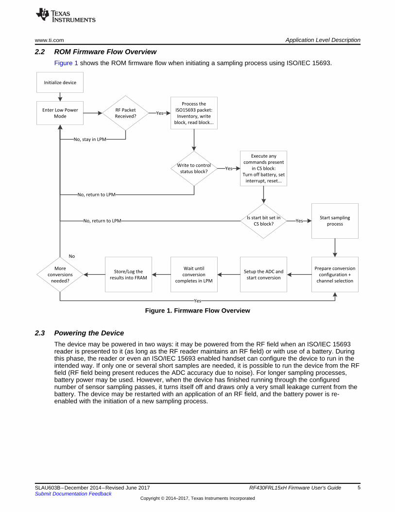
2.1 Function OverviewRegisters exist in FRAM memory which control the ROM firmware operation. Based on the settings writtento the control and status block, the device samples through the selected sensors (reference/ADC1,thermistor/ADC2, ADC0, digital), after the sample is taken, a min, max or averaging is done, if selected,and then it is stored in FRAM (or RAM) consecutively. Setting up the configuration may be done throughthe ISO/IEC 15693 interface or through I2C or SPI. The interfaces merely are able to read and write to theFRAM (or RAM) memory. After all of the readings are stored, the device can turn off the power from thebattery, if it has been so configured. The samples that were stored may be read through the RF ISO/IEC15693 interface or through I2C or SPI.
Initialize device
Enter Low Power
Mode
RF Packet
Received?
Process the
ISO15693 packet:
Inventory, write
block, read block...
Yes
Write to control
status block?
No, stay in LPM
Is start bit set in
CS block?
No, return to LPM
Yes
Start sampling
processYes
Execute any
commands present
in CS block:
Turn off battery, set
interrupt, reset...
No, return to LPM
Prepare conversion
configuration +
channel selection
Setup the ADC and
start conversion
Wait until
conversion
completes in LPM
Store/Log the
results into FRAM
More
conversions
needed?
Yes
No
www.ti.com Application Level Description
5SLAU603B–December 2014–Revised June 2017Submit Documentation Feedback
Copyright © 2014–2017, Texas Instruments Incorporated
RF430FRL15xH Firmware User's Guide
2.2 ROM Firmware Flow OverviewFigure 1 shows the ROM firmware flow when initiating a sampling process using ISO/IEC 15693.
Figure 1. Firmware Flow Overview
2.3 Powering the DeviceThe device may be powered in two ways: it may be powered from the RF field when an ISO/IEC 15693reader is presented to it (as long as the RF reader maintains an RF field) or with use of a battery. Duringthis phase, the reader or even an ISO/IEC 15693 enabled handset can configure the device to run in theintended way. If only one or several short samples are needed, it is possible to run the device from the RFfield (RF field being present reduces the ADC accuracy due to noise). For longer sampling processes,battery power may be used. However, when the device has finished running through the configurednumber of sensor sampling passes, it turns itself off and draws only a very small leakage current from thebattery. The device may be restarted with an application of an RF field, and the battery power is re-enabled with the initiation of a new sampling process.
Application Level Description www.ti.com
6 SLAU603B–December 2014–Revised June 2017Submit Documentation Feedback
Copyright © 2014–2017, Texas Instruments Incorporated
RF430FRL15xH Firmware User's Guide
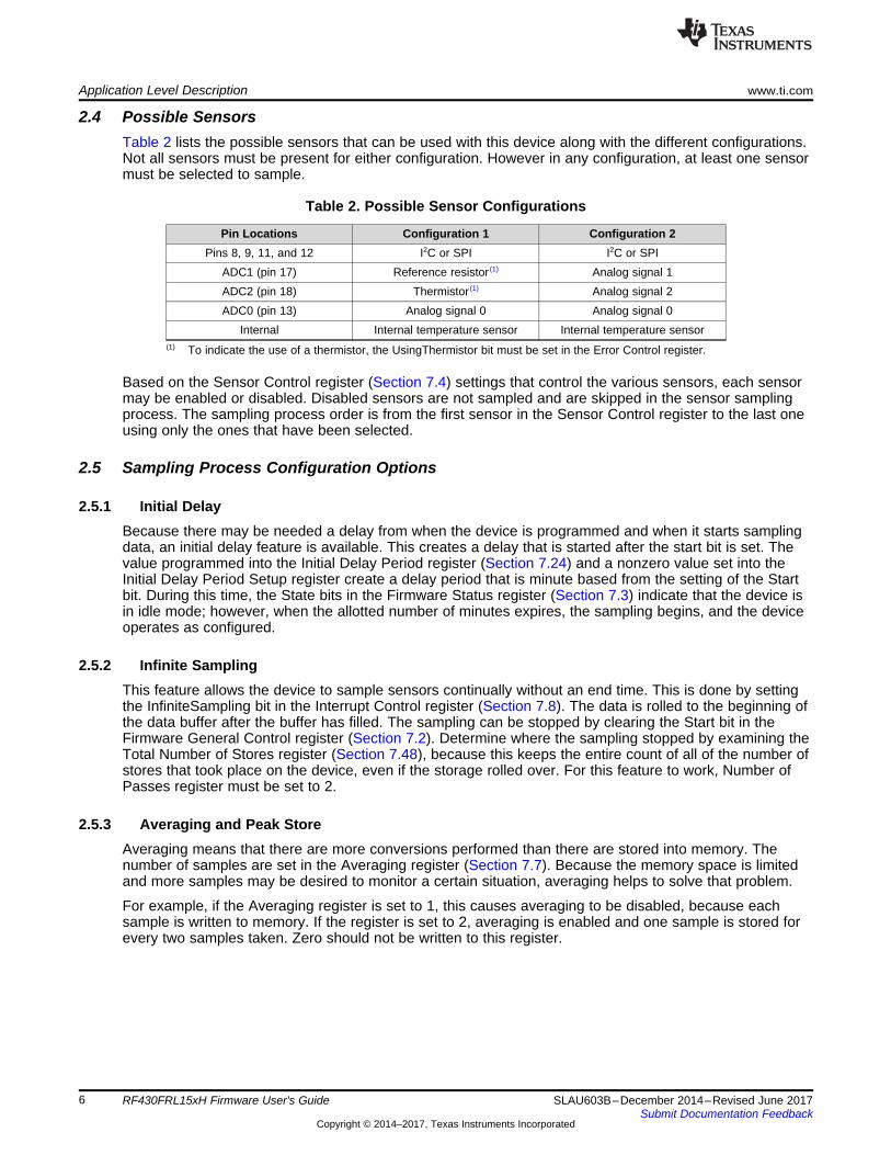
2.4 Possible SensorsTable 2 lists the possible sensors that can be used with this device along with the different configurations.Not all sensors must be present for either configuration. However in any configuration, at least one sensormust be selected to sample.
(1) To indicate the use of a thermistor, the UsingThermistor bit must be set in the Error Control register.
Table 2. Possible Sensor Configurations
Pin Locations Configuration 1 Configuration 2Pins 8, 9, 11, and 12 I2C or SPI I2C or SPI
ADC1 (pin 17) Reference resistor (1) Analog signal 1ADC2 (pin 18) Thermistor (1) Analog signal 2ADC0 (pin 13) Analog signal 0 Analog signal 0
Internal Internal temperature sensor Internal temperature sensor
Based on the Sensor Control register (Section 7.4) settings that control the various sensors, each sensormay be enabled or disabled. Disabled sensors are not sampled and are skipped in the sensor samplingprocess. The sampling process order is from the first sensor in the Sensor Control register to the last oneusing only the ones that have been selected.
2.5 Sampling Process Configuration Options
2.5.1 Initial DelayBecause there may be needed a delay from when the device is programmed and when it starts samplingdata, an initial delay feature is available. This creates a delay that is started after the start bit is set. Thevalue programmed into the Initial Delay Period register (Section 7.24) and a nonzero value set into theInitial Delay Period Setup register create a delay period that is minute based from the setting of the Startbit. During this time, the State bits in the Firmware Status register (Section 7.3) indicate that the device isin idle mode; however, when the allotted number of minutes expires, the sampling begins, and the deviceoperates as configured.
2.5.2 Infinite SamplingThis feature allows the device to sample sensors continually without an end time. This is done by settingthe InfiniteSampling bit in the Interrupt Control register (Section 7.8). The data is rolled to the beginning ofthe data buffer after the buffer has filled. The sampling can be stopped by clearing the Start bit in theFirmware General Control register (Section 7.2). Determine where the sampling stopped by examining theTotal Number of Stores register (Section 7.48), because this keeps the entire count of all of the number ofstores that took place on the device, even if the storage rolled over. For this feature to work, Number ofPasses register must be set to 2.
2.5.3 Averaging and Peak StoreAveraging means that there are more conversions performed than there are stored into memory. Thenumber of samples are set in the Averaging register (Section 7.7). Because the memory space is limitedand more samples may be desired to monitor a certain situation, averaging helps to solve that problem.
For example, if the Averaging register is set to 1, this causes averaging to be disabled, because eachsample is written to memory. If the register is set to 2, averaging is enabled and one sample is stored forevery two samples taken. Zero should not be written to this register.
www.ti.com Application Level Description
7SLAU603B–December 2014–Revised June 2017Submit Documentation Feedback
Copyright © 2014–2017, Texas Instruments Incorporated
RF430FRL15xH Firmware User's Guide
When more samples are taken than are stored, there are several processes that may be done on theresults. The selecting of either choosing the minimum, maximum, first or averaging the results may beconfigured in the sensor-specific Alarm Configuration register (see Section 7.40 through Section 7.46)(except for Internal Alarm Configuration register). Depending on the specific alarm configuration register,the value chosen for peak store (a field of alarm configuration register) determines which sample is stored.There are several options. The lowest or highest that was sampled during those groups of samples (set inthe Averaging register) is stored into memory. The process repeats until the Number of Passes register(Section 7.6) samples have been completed.
Therefore, the actual numbers of samples that are taken can be determined using this equation:Total number of samples = (Number of Passes register) × (Averaging register) × (Number of selectedsensors)
This formula is valid only if the sensors have a skip counter set to 1 (that is, no sensors are beingskipped).
There is another feature that may be done on the averaged samples. If alarm or interrupt capability isneeded, that may be enabled in the specific Alarm Configuration register. If enabled, each sample that istaken (does not matter if it is stored into memory or not) is compared to the high and low thresholds set forthat sensor. If the thresholds are crossed, an alarm bit is set in the same register. In addition, if the Alarmbit is set in the Firmware General Control register and the interrupt is enabled in the specific alarmconfiguration register, the interrupt is asserted on the interrupt pin of the device.
2.5.4 Sensor Sampling Duty CycleThe sensor duty cycle can be configured using the Sensor Skip Count register for each sensor. When thisregister is set to 0, the sensor is sampled every time that its turn comes up. If the register is set to a valueother than 0, the sensor is skipped that number of times. For example, if the register is set to 1, the sensorhas a duty cycle of 50%.
If averaging or peak storing modes are used with a skip count, the skip count creates a duty cycle on thenumber of stored values for that sensor. For example, if ten stored values are expected (Number ofSamples = 10), and the averaging is set to 5, this configuration results in 50 samples (5 × 10), and with aduty cycle of 50% (skip count = 1), the number of logged values is 5 (instead of 10). However, for samplesthat were logged, the number of samples that were taken remain at 5 as set in the averaging register.
2.5.5 Custom TimeIf the preprogrammed time values in the Frequency register are not acceptable, a different time may beused by programming the Custom Timer Value register with the number of milliseconds that is neededbetween passes. To use this option the Frequency register must be set to custom time option.
The custom time register value is controllable to milliseconds for up to 65 seconds. Any value higher than65 seconds (65535), is only minute controllable. For example, entering 110000 ms (110 seconds) into thecustom time register gives an effective frequency of 2 minutes even though the entry was in milliseconds.
2.5.6 Software ResetWhen the Reset register is set, it causes the device to perform a power-up clear (PUC). The register iscleared after the reset is complete.
2.6 Sensor ConfigurationFor each sensor (excluding the external digital sensors), various parameters may be set, such as digitalfilter type, oversampling rate, gain, and virtual ground. Each of these parameters is explained in thefollowing sections. The ground reference can be changed for external analog sensors. Selecting theVirtual Ground setting causes SVSS to be raised to approximately 125 mV. This is important, because thevoltages close to ground can have some minor error due to the ADC nonlinear behavior at those levels.

Application Level Description www.ti.com
8 SLAU603B–December 2014–Revised June 2017Submit Documentation Feedback
Copyright © 2014–2017, Texas Instruments Incorporated
RF430FRL15xH Firmware User's Guide
2.6.1 Sensor GainThe ADC has an analog front end that includes a PGA (see the data sheet, RF430FRL15xH NFC ISO15693 Sensor Transponder). The PGA allows amplification of 1x, 2x, 4x, or 8x. Make sure that the inputsignal does not reach the power rails. Full voltage swing is 0 V to 0.9 V.
2.6.2 Filter TypeTwo different filters are available. Each has its advantages. They are the moving average filter and thecascaded integrator-comb (CIC) filter. See the data sheet for more information.
2.6.3 SD RateThis parameter controls the filter decimation ratio (for CIC filter) or the number of samples to average (forthe moving average filter). Generally, the higher this number is, the longer the conversion takes tocomplete, but the accuracy of the result increases.
2.6.4 Virtual GroundThe device can ground the ADC to actual ground, or it can internally isolate the ground and drive itinternally with a DC signal, raising it a little. (The actual voltage driven is given in the data sheet). This isneeded, because the ADC does not have the best linearity near the ground. Raising ground above thisvoltage range allows for correct conversions in all cases.
The application should use the same ground (actual or virtual) for all analog sensors. It is notrecommended to change the ground from sensor to sensor, because changing the ground level needstime to stabilize, and there is usually not enough time for stabilization between measurements.
2.6.5 Digital Filter TypesAll of the analog sensors are sampled using the internal sigma-delta 14-bit analog-to-digital converter. Theconverter is based on a first-order sigma-delta modulator whose output is oversampled followed by adigital decimation filter. Two types of filter are available: a cascaded integrator-comb (CIC) filter withprogrammable rate change from 32 to 2048, and a moving average filter with programmable number ofsamples. Additional filtering can be done in software (by using the averaging functionality of the device, forexample). Each sensor may be configured to use either of the two digital filters with a different number ofsamples. For the CIC filter after switching to from another channel, or if the gain is changed, to allow thefilter to settle; only every second conversion is used.
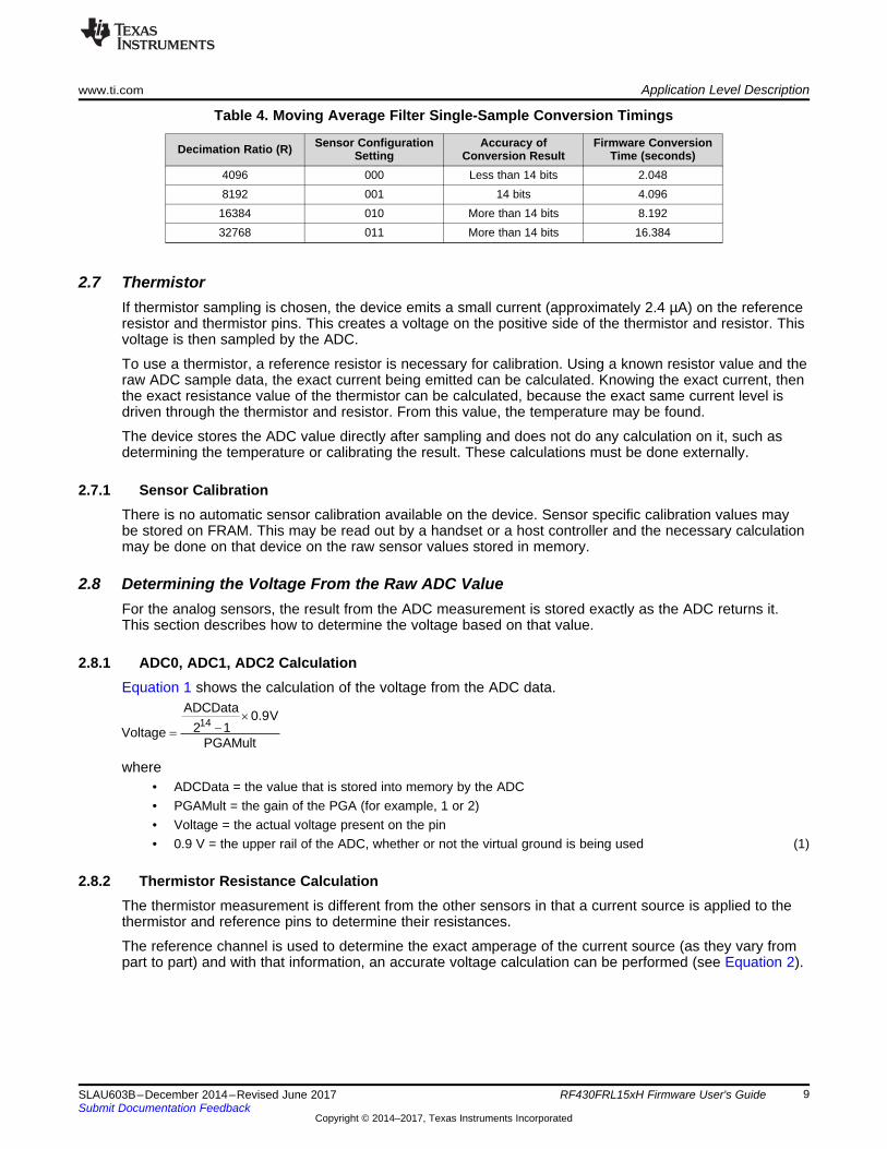
2.6.6 Analog-to-Digital Conversion TimingsTable 3 and Table 4 list the single-sample conversion times for the CIC filter and moving average filter,respectively.
Table 3. CIC Filter Single-Sample Conversion Timings
Decimation Ratio(R)
SensorConfiguration
Setting
Accuracy ofConversionResult (bits)
Conversion Time(ms)
FirmwareConversion Time
(ms)(2 cycles if
change to gain,channel or R)
32 000 7 16 3264 001 9 32 64128 010 10 64 128256 011 12 128 256512 100 13 256 5121024 101 15 512 10242048 110 16 1024 2048
14ADCData
0.9V2 1Voltage
PGAMult
u
�
www.ti.com Application Level Description
9SLAU603B–December 2014–Revised June 2017Submit Documentation Feedback
Copyright © 2014–2017, Texas Instruments Incorporated
RF430FRL15xH Firmware User's Guide
Table 4. Moving Average Filter Single-Sample Conversion Timings
Decimation Ratio (R) Sensor ConfigurationSetting
Accuracy ofConversion Result
Firmware ConversionTime (seconds)
4096 000 Less than 14 bits 2.0488192 001 14 bits 4.096
16384 010 More than 14 bits 8.19232768 011 More than 14 bits 16.384
2.7 ThermistorIf thermistor sampling is chosen, the device emits a small current (approximately 2.4 µA) on the referenceresistor and thermistor pins. This creates a voltage on the positive side of the thermistor and resistor. Thisvoltage is then sampled by the ADC.
To use a thermistor, a reference resistor is necessary for calibration. Using a known resistor value and theraw ADC sample data, the exact current being emitted can be calculated. Knowing the exact current, thenthe exact resistance value of the thermistor can be calculated, because the exact same current level isdriven through the thermistor and resistor. From this value, the temperature may be found.
The device stores the ADC value directly after sampling and does not do any calculation on it, such asdetermining the temperature or calibrating the result. These calculations must be done externally.
2.7.1 Sensor CalibrationThere is no automatic sensor calibration available on the device. Sensor specific calibration values maybe stored on FRAM. This may be read out by a handset or a host controller and the necessary calculationmay be done on that device on the raw sensor values stored in memory.
2.8 Determining the Voltage From the Raw ADC ValueFor the analog sensors, the result from the ADC measurement is stored exactly as the ADC returns it.This section describes how to determine the voltage based on that value.
2.8.1 ADC0, ADC1, ADC2 CalculationEquation 1 shows the calculation of the voltage from the ADC data.
where• ADCData = the value that is stored into memory by the ADC• PGAMult = the gain of the PGA (for example, 1 or 2)• Voltage = the actual voltage present on the pin• 0.9 V = the upper rail of the ADC, whether or not the virtual ground is being used (1)
2.8.2 Thermistor Resistance CalculationThe thermistor measurement is different from the other sensors in that a current source is applied to thethermistor and reference pins to determine their resistances.
The reference channel is used to determine the exact amperage of the current source (as they vary frompart to part) and with that information, an accurate voltage calculation can be performed (see Equation 2).
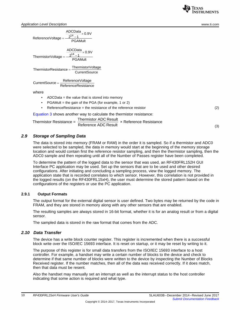
Thermistor ADC ResultThermistor Resistance = × Reference Resistance
Reference ADC Result
14ADCData
0.9V2 1ReferenceVoltage
PGAMult
u
�
14ADCData
0.9V2 1ThermistorVoltage
PGAMult
u
�
ReferenceVoltageCurrentSource
ReferenceResistance
ThermistorVoltageThermistorResistance
CurrentSource
Application Level Description www.ti.com
10 SLAU603B–December 2014–Revised June 2017Submit Documentation Feedback
Copyright © 2014–2017, Texas Instruments Incorporated
RF430FRL15xH Firmware User's Guide
where• ADCData = the value that is stored into memory• PGAMult = the gain of the PGA (for example, 1 or 2)• ReferenceResistance = the resistance of the reference resistor (2)
Equation 3 shows another way to calculate the thermistor resistance:
(3)
2.9 Storage of Sampling DataThe data is stored into memory (FRAM or RAM) in the order it is sampled. So if a thermistor and ADC0were selected to be sampled, the data in memory would start at the beginning of the memory storagelocation and would contain first the reference resistor sampling, and then the thermistor sampling, then theADC0 sample and then repeating until all of the Number of Passes register have been completed.
To determine the pattern of the logged data to the sensor that was used, an RF430FRL152H GUIInterface PC application may be used. Set up the sensors that are to be used and other desiredconfigurations. After initiating and concluding a sampling process, view the logged memory. Theapplication state that is recorded correlates to which sensor. However, this correlation is not provided inthe logged results (on the RF430FRL15xH), the user must determine the stored pattern based on theconfigurations of the registers or use the PC application.
2.9.1 Output FormatsThe output format for the external digital sensor is user defined. Two bytes may be returned by the code inFRAM, and they are stored in memory along with any other sensors that are enabled.
The resulting samples are always stored in 16-bit format, whether it is for an analog result or from a digitalsensor.
The sampled data is stored in the raw format that comes from the ADC.
2.10 Data TransferThe device has a write block counter register. This register is incremented when there is a successfulblock write over the ISO/IEC 15693 interface. It is reset on startup, or it may be reset by writing to it.
The purpose of this register is for small data transfers from the ISO/IEC 15693 interface to a hostcontroller. For example, a handset may write a certain number of blocks to the device and check todetermine if that same number of blocks were written to the device by inspecting the Number of BlocksReceived register. If the number matches, then all of the data was received correctly. If it does match,then that data must be resent.
Also the handset may manually set an interrupt as well as the interrupt status to the host controllerindicating that some action is required and what type.
www.ti.com Application Level Description
11SLAU603B–December 2014–Revised June 2017Submit Documentation Feedback
Copyright © 2014–2017, Texas Instruments Incorporated
RF430FRL15xH Firmware User's Guide
2.11 FRAM Memory MapTable 5 summarizes the FRAM memory map.
Table 5. FRAM Memory Map
Memory Range Length DescriptionFFFFh-FFD0h 48 Interrupt vectors, boot data
FFCEh-XXXXh 0 to X
Patch (driver) functions definition table.Starts with CECEh, then patch number and followed by address of thepatch function in the FRAM memory space; pairs repeat until ended byCECEh. See Section 9 for more information.
Patch function definitions if exist 0 to X
FCA0h-F8B0h (default 504 samples)FFD0h-F8B0h (912 samples) 504 or greater
Sensor data storageDefault 504 locations, but may be increased if needed. Counts up.Maximum 912 samples is possible (FRAM storage)
F8AFh-F868h 72 Virtual registers that control device functionality
F867h-F840h 40 Lock blocks memory table.Not accessible through ISO/IEC 15693.
2.12 Errors
2.12.1 Timing ErrorAfter passing through the selected sensors, the device stores the results in FRAM. If more than one passis configured (through the Number of Passes register), depending on the value in Frequency register, thedevice waits a certain time until it starts the next pass through the sensors. The available wait times rangefrom half a second to 24 hours. For the very short wait times, the amount of time needed to sample all ofthe selected sensors must be considered. If the previous pass is in the process of being sampled and thetime for the next pass is reached, a collision occurs (the timing information is included in the followingsection). If a collision occurs, the Timing Error bit is set in the State field (indicating an error) in theFirmware Status register. In addition, the acquisition process is stopped and the device may turn off (ifusing battery power and it has been configured to do so). The timing error register is reset by either asoftware reset or by starting a new sample process.
2.12.2 OverflowIf the number of samples stored exceeds Logging Memory Size register during runtime, the previous dataremains in memory, the Overflow bit in the Status register is set, the State field in the Status register is setto 3 (indicating an error), the sample process stops, and the battery switch turns off, if configured to do so.The overflow register can be reset either by a software reset or by starting a new sample process.
2.12.3 On Boot UpIf the device resets unexpectedly, the reset cause can be logged on boot up if this is needed. When thedevice powers up, it checks the reset reason (if CheckResetError is set in the Error Control register) and,if the reset was due to an error, it is logged at the end of the data storage. The reset conditions are storedone after another (as they come from the SYSRSTIV hardware register) and end with the word 0xEAFE.
2.12.4 Power Management ErrorsIf there is a PMM event like VDD_2X or VDDB low, the error is logged in the Error Control register bysetting the corresponding bits.
2.12.5 Application CRCApplication CRC is a feature on the device, where the CRC for the application firmware can be generatedand placed in the CRC signature location in the signature table. The CRC Length and Value are locatedwithin the IV at 0xFF8A-0xFF8D.
Sensor Sampling Scheduler www.ti.com
12 SLAU603B–December 2014–Revised June 2017Submit Documentation Feedback
Copyright © 2014–2017, Texas Instruments Incorporated
RF430FRL15xH Firmware User's Guide
The CRC signature check happens when user application is present (that is, Reset Vector is not 0xFFFF)and the RF Loader signature is not set to disabled.
During the CRC check: the bootcode (BC) first checks the CRC length value; if CRC length is 0x0000 or0xFFFF, then the CRC was not loaded by the user, so a CRC of the user application memory is notperformed, and the bootcode assumes that it is acceptable to start the user application (if present).Therefore, for critical applications, the user needs to update the CRC Length field (with the number ofbytes from 0x10000 backwards, to be checked) and make sure that the length does not equal 0xFFFF.
If the proper CRC length and value signatures are loaded by the user, then the BC performs the CRCoperation with CCITT CRC16 from the end of the memory in the direction of memory start until the Lengthis reached. The CRC result is checked against the CRC value signature. This way the customer canprotect his own code by setting the CRC Length up to the used memory size of his application. Thisprevents bricking the device with corrupted User Code and prevents unexpected device behavior in criticalapplications.
The only drawback is the increased startup time of approximately 8 µs per memory word. For example,the check requires approximately 200 µs to check the Interrupt vector and signature table, and 8 ms forthe complete FRAM memory.
NOTE: The CRC function that computes the CRC of a specified memory block is present in theROM memory at 0x4400 to 0x47FF, as part of the Fixed Functions that are used by the BCand user application. This makes sure that the CRC function is not corrupted.
3 Sensor Sampling Scheduler
3.1 Examples
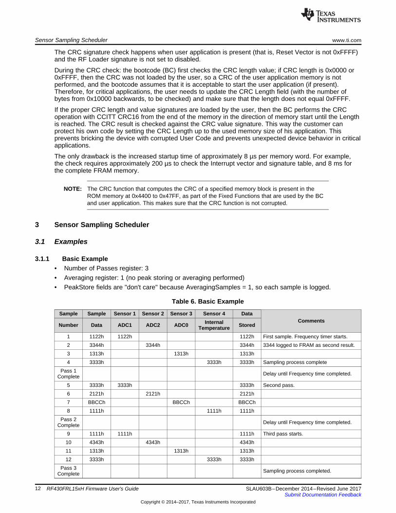
3.1.1 Basic Example• Number of Passes register: 3• Averaging register: 1 (no peak storing or averaging performed)• PeakStore fields are "don't care" because AveragingSamples = 1, so each sample is logged.
Table 6. Basic Example
Sample Sample Sensor 1 Sensor 2 Sensor 3 Sensor 4 DataComments
Number Data ADC1 ADC2 ADC0 InternalTemperature Stored
1 1122h 1122h 1122h First sample. Frequency timer starts.2 3344h 3344h 3344h 3344 logged to FRAM as second result.3 1313h 1313h 1313h4 3333h 3333h 3333h Sampling process complete
Pass 1Complete Delay until Frequency time completed.
5 3333h 3333h 3333h Second pass.6 2121h 2121h 2121h7 BBCCh BBCCh BBCCh8 1111h 1111h 1111h
Pass 2Complete Delay until Frequency time completed.
9 1111h 1111h 1111h Third pass starts.10 4343h 4343h 4343h11 1313h 1313h 1313h12 3333h 3333h 3333h
Pass 3Complete Sampling process completed.

www.ti.com Sensor Sampling Scheduler
13SLAU603B–December 2014–Revised June 2017Submit Documentation Feedback
Copyright © 2014–2017, Texas Instruments Incorporated
RF430FRL15xH Firmware User's Guide
Table 7. Layout of Data Logged Into Memory (From Table 6)
Address Byte 0 1 2 3 4 5 6 70xF8B0 22 11 44 33 13 13 33 330xF8B8 33 33 21 21 CC BB 11 110xF8C0 11 11 43 43 13 13 33 33
3.1.2 Advanced Example• Number of Passes register: 3• Averaging register: 2 (peak store or averaging is performed)
Table 8. Example ScheduleSample Sample Reference Therm. ADC0 Internal Digital Data Averaging = 2
Number Data Highest HighestSkip 1 Avg Lowest
Skip 2 First Logged Comments
1 3333 3333 3333 temporarily stored
2 1212 1212 1212 is temporarily stored, highest value rightnow, out of 1
3 2121 2121 ADC0 set to averaging, 2121 is temporarilystored
4 BBCC BBCC BBCC is currently the lowest
5 1122 1122 1122 Digital sensor is set to use the first value out oftwo passes, 1122 logged right away
First sampling pass complete. Delayed by theamount of time set in frequency register. Timer isstarted at the beginning of the sampling pass(that is before sample pass 1)
6 1111 1111 Value stored, need thermistor result to determineif keep
7 2222 2222 1111 2222 > 1212 therefore log 1111 (associatedreference resistor value)
2222 2222 > 1212 therefore store 2222 next (highestresult out of two passes)
8 4343 4343 3232 4343 and 2121 averaged = 3232, logged
9 1313 1313 1313 1313 < BBCC therefore 1313 logged now
Skip Skip digital sensor measurement, because onlyfirst kept out of 2 passes (avg =2)
Round 2Delayed by the amount set in Frequencyregister. New averaging round (2 passesbecause average = 2).
Skip Skip Skip reference and thermistor measurementstogether because skip = 1
10 3333 3333 Sample ADC0 and temporarily store 3333
Skip Skip Internal temperature sensor due to skip = 2for internal temperature sensor
11 3344 3344 3344 Store 3344 for digital sensor because alwayskeep the first value only on beginning of round
Skip Skip Reference and thermistor have skip = 1, so thewhole averaging round (2 passes is skipped)
Pass complete. Delayed by the amount inFrequency register.
12 5555 5555 4444 5555 and 3333 averaged is 4444, log now
Skip Internal temperature sensor is skipped becauseskip = 2, currently in the first skip round
Skip Digital sensor is set to use the first value, thathas already been stored. Skip this sample.
Round 3 Frequency delay. New averaging round ( 2passes because average = 2)
13 2121 2121 Stored when the associated thermistormeasurement is used, stored temporarily

RF Stack www.ti.com
14 SLAU603B–December 2014–Revised June 2017Submit Documentation Feedback
Copyright © 2014–2017, Texas Instruments Incorporated
RF430FRL15xH Firmware User's Guide
Table 8. Example Schedule (continued)Sample Sample Reference Therm. ADC0 Internal Digital Data Averaging = 2
Number Data Highest HighestSkip 1 Avg Lowest
Skip 2 First Logged Comments
14 BBCC BBCC Stored temporarily
15 1111 1111 Stored temporarily
Skip Internal temperature sensor is skipped becauseskip = 2, currently in the second skip round
16 1122 1122 1122 Digital temperature sensor always logs the firstvalue of the round
Pass complete. Timer delay.
17 1111 1111 stored temporarily
18 4343 4343 2121 BBCC > 4343 therefore associated 2121 loggedfirst
BBCC BBCC stored next
19 1313 1313 1212 1111 and 1313 averaged = 1212, stored now
Skip Internal temperature sensor is skipped becauseskip = 2, currently in the second skip round
SkipDigital sensor is set to use the first value, thathas already been stored. Skip this sample.Sampling process complete.
4 RF Stack
4.1 SummaryThe ISO/IEC 15693 stack is a separate part of the ROM on the RF430. It handles both the incoming RFcommands as well as allows the firmware on the device to issue these commands themselves. The stacksupports multiple block sizes communication. To support this flexibility, an unconventional configurationmethod had to be used.
The ISO/IEC 15693 stack allows read and write access to the FRAM memory and using customcommands access to the RAM memory as well. All memory has potential to be locked so that further writeaccess is not possible. Change from block size of 4 or 8 can be done through a write to a special block.
4.2 Supported CommandsAll the minimum ISO commands are supported as well as the additional standard ones. They are:• Inventory• Read Single Block• Read Multiple Blocks• Select• Write Single Block• Write Multiple Blocks• Lock Block• Stay Quite• Reset to Ready• Get System Info

www.ti.com RF Stack
15SLAU603B–December 2014–Revised June 2017Submit Documentation Feedback
Copyright © 2014–2017, Texas Instruments Incorporated
RF430FRL15xH Firmware User's Guide
In addition there are custom commands that allow access to RAM memory. These commands areidentical to the standard commands, except they have a 16-bit block number field. This allows them agreater memory access range.• Custom Read Single Block• Custom Read Multiple Block• Custom Write Single Block• Custom Write Multiple Block• Custom Lock Block
These custom commands may be used to access FRAM; however, they must follow the paging protocol.
4.3 Supported ConfigurationsUsing 8-byte block mode, the maximum ISO/IEC 15693 block size can cover 2KB of memory, which forFRAM memory size allows full coverage. However in 4-byte block sizes, this is not possible. To allow fullcoverage of the FRAM in 4-byte block mode, paging must be used. This allows full access to FRAM by aconfiguration block (0xFF) that is accessible in all cases. The configuration block is defined in theISOBlockSize field in the Firmware Control register (see Section 7.54).
This block also allows reading and answers with the selected block type, either 4 or 8 bytes. This block isvirtual in that its location is different from where block 0xFF should be. This is handled internally. Thereason block 0xFF was chosen is because it was not used in either block size mode.
Because data can be stored in RAM or FRAM, access to RAM using ISO/IEC 15693 is also included.Access to RAM memory can be done using custom commands. These custom commands differ very littlefrom their standard commands (such as read and write block) in that they use only a 16-bit block numberinstead of an 8-bit one (see Section 4.7).
4.4 Memory UseTable 9 and Table 10 describe the ISO/IEC 15693 lock block memory area.
Table 9. ISO/IEC 15693 Lock Block Memory Area
Start Address Stop Address Size Purpose0xF840 0xF867 40 bytes Bit array that describes locked blocks (0 = locked)
Table 10. ISO/IEC 15693 Memory Description
Field Name ValueFRAM Memory Start 0xF840
ISO/IEC 15693 Blocks Start 0xF868ISO/IEC 15693 Blocks End 0xFFFF
ISO/IEC 15693 Memory Size 1944 bytesISO/IEC 15693 Number of Blocks 243 (F3h)
ISO/IEC 15693 Block Size 4 or 8 bytes, depending on configuration of setting in virtual block number 0xFF
RF Stack www.ti.com
16 SLAU603B–December 2014–Revised June 2017Submit Documentation Feedback
Copyright © 2014–2017, Texas Instruments Incorporated
RF430FRL15xH Firmware User's Guide
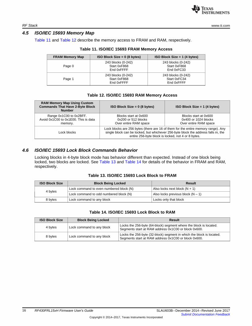
4.5 ISO/IEC 15693 Memory MapTable 11 and Table 12 describe the memory access to FRAM and RAM, respectively.
Table 11. ISO/IEC 15693 FRAM Memory Access
FRAM Memory Map ISO Block Size = 0 (8 bytes) ISO Block Size = 1 (4 bytes)
Page 0243 blocks (0-242)
Start 0xF868End 0xFFFF
243 blocks (0-242)Start 0xF868End 0xFC33
Page 1243 blocks (0-242)
Start 0xF868End 0xFFFF
243 blocks (0-242)Start 0xFC34End 0xFFFF
Table 12. ISO/IEC 15693 RAM Memory Access
RAM Memory Map Using CustomCommands That Have 2-Byte Block
NumberISO Block Size = 0 (8 bytes) ISO Block Size = 1 (4 bytes)
Range 0x1C00 to 0x2BFF.Avoid 0x1C00 to 0x1E00. This is data
memory.
Blocks start at 0x6000x200 or 512 blocks
Over entire RAM space
Blocks start at 0x6000x400 or 1024 blocks
Over entire RAM space
Lock blocksLock blocks are 256 bytes (there are 16 of them for the entire memory range). Anysingle block can be locked, but whichever 256-byte block the address falls in, the
entire 256-byte block is locked, not 4 or 8 bytes.
4.6 ISO/IEC 15693 Lock Block Commands BehaviorLocking blocks in 4-byte block mode has behavior different than expected. Instead of one block beinglocked, two blocks are locked. See Table 13 and Table 14 for details of the behavior in FRAM and RAM,respectively.
Table 13. ISO/IEC 15693 Lock Block to FRAM
ISO Block Size Block Being Locked Result
4 bytesLock command to even numbered block (N) Also locks next block (N + 1)Lock command to odd numbered block (N) Also locks previous block (N – 1)
8 bytes Lock command to any block Locks only that block
Table 14. ISO/IEC 15693 Lock Block to RAM
ISO Block Size Block Being Locked Result
4 bytes Lock command to any block Locks the 256-byte (64-block) segment where the block is located.Segments start at RAM address 0x1C00 or block 0x600.
8 bytes Lock command to any block Locks the 256-byte (32-block) segment in which the block is located.Segments start at RAM address 0x1C00 or block 0x600.
www.ti.com RF Stack
17SLAU603B–December 2014–Revised June 2017Submit Documentation Feedback
Copyright © 2014–2017, Texas Instruments Incorporated
RF430FRL15xH Firmware User's Guide
4.7 Custom CommandsThese commands are necessary because this version of device has more than 2KB of memory. Currentlythe ISO/IEC 15693 standard does not have a standard way of supporting memory ranges over 2KB.
These are the custom commands that this stack supports. The differences are that these commands arein the custom command format (command code + manufacturer code) and that the block number is in16‑bit length and not 8-bit length as the standard commands use.
Table 15 is a list of the custom commands with their corresponding command code:
Table 15. Custom Commands Type
Command Type Command CodeCustom Read Single with 16-bit block number 0xC0Custom Write Single with 16-bit block number 0xC1Custom Lock Block with 16-bit block number 0xC2
Custom Read Multiple with 16-bit block number 0xC3Custom Write Multiple with 16-bit block number 0xC4
4.8 Custom Read Single With 16-Bit Block Number
Table 16. Custom Read Single Block Command Packet Setup
Field Name Number of Bytes ValueSOFFlags 1 Any
Command Code 1 0xC0Mfg Code 1 0x07
UID (optional) 8 AnyBlock Number
(LSB first) 2 0x600-0xA00 (RAM, 4-byte block)0x600-0x800 (RAM, 8-byte block)
CRC16 2EOF
4.9 Custom Write Single With 16-Bit Block Number
Table 17. Custom Write Single Command Packet Setup
Field Name Number of Bytes ValueSOFFlags 1 Any
Command Code 1 0xC1Mfg Code 1 0x07
UID (optional) 8 AnyBlock Number
(LSB first) 2 0x600-0xA00 (RAM, 4-byte block)0x600-0x800 (RAM, 8-byte block)
Data 8 anyCRC16 2
EOF
RF Stack www.ti.com
18 SLAU603B–December 2014–Revised June 2017Submit Documentation Feedback
Copyright © 2014–2017, Texas Instruments Incorporated
RF430FRL15xH Firmware User's Guide
4.10 Custom Lock Block With 16-Bit Block Number
Table 18. Custom Lock Block Command Packet Setup
Field Name Number of Bytes ValueSOFFlags 1 Any
Command Code 1 0xC2Mfg Code 1 0x07
UID (optional) 8 AnyBlock Number
(LSB first) 2 0x600-0xA00 (RAM, 4-byte block)0x600-0x800 (RAM, 8-byte block)
Data 8 anyCRC16 2
EOF
4.11 Custom Read Multiple With 16-Bit Block Number
Table 19. Custom Read Multiple Command Packet Setup
Field Name Number of Bytes ValueSOFFlags 1 Any
Command Code 1 0xC3Mfg Code 1 0x07
UID (optional) 8 AnyBlock Number
(LSB first) 2 0x600-0xA00 (RAM, 4-byte block)0x600-0x800 (RAM, 8-byte block)
Number of Blocks 1 0-2 (8-block)0-5 (4-block)CRC16 2
EOF
4.12 Custom Write Multiple With 16-Bit Block Number
Table 20. Custom Write Multiple Packet Setup
Field Name Number of Bytes ValueSOFFlags 1 Any
Command Code 1 0xC4Mfg Code 1 0x07
UID (optional) 8 AnyFirst Block Number
(LSB first) 2 0x600-0xA00 (RAM, 4-byte block)0x600-0x800 (RAM, 8-byte block)
Number of Blocks 1 0-2 (8-block)0-5 (4-block)Data 8-24 any
CRC16 2EOF
www.ti.com RF Stack
19SLAU603B–December 2014–Revised June 2017Submit Documentation Feedback
Copyright © 2014–2017, Texas Instruments Incorporated
RF430FRL15xH Firmware User's Guide
4.13 LimitationsCurrently addressed write multiple command with three blocks is not supported, because this commandexceeds the input buffer on the device of 32 bytes. If this is attempted, an error code of 0x0F is returned.The stack does not execute the command.
4.14 RF Stack Memory Access ProtectionIn some cases, it may be needed to prevent access to some portions of the FRAM memory from RFaccess. An option was created that prevents reading or writing of FRAM memory based on an address setin a FRAM register. This register is called FRAMAccessLimit, and it prevents reading or writing of FRAMmemory from the address FFFFh to the address set in it.
For example, if the FRAMAccessLimit is set to FF00h, the RF stack would respond with an error code(that the block does not exist) to any FRAM memory access between FF01h and FFFFh. By default, thisregister is set to 0xFFFF and allows the full FRAM access.
An example use case is if the user has developed some code that is stored in the high FRAM memorylocations. The FRAMAccessLimit could be set to prevent reading and writing to that code. The mainbenefit of this feature is that it prevents reading of the memory. Write protection is accomplished with lockblocks on the ISO/IEC 15693 interface.
5 Interfacing a Host Controller
5.1 Host ControllerIf an external digital sensor is not used, a host controller can be interfaced to the SPI or I2C bus. Themaster/slave select pin (19) must be set to slave option or pulled high. The host controller has read andwrite access to the memory space of the device. This allows it to initiate sensor sampling if necessary.Cooperation between the ISO/IEC 15693 interface and a host controller is possible.
5.2 I2C and SPI Host Controller Communication Protocol
NOTE: RF430FRL153H does not have an eUSCI module, thus this section does not apply to thatdevice.
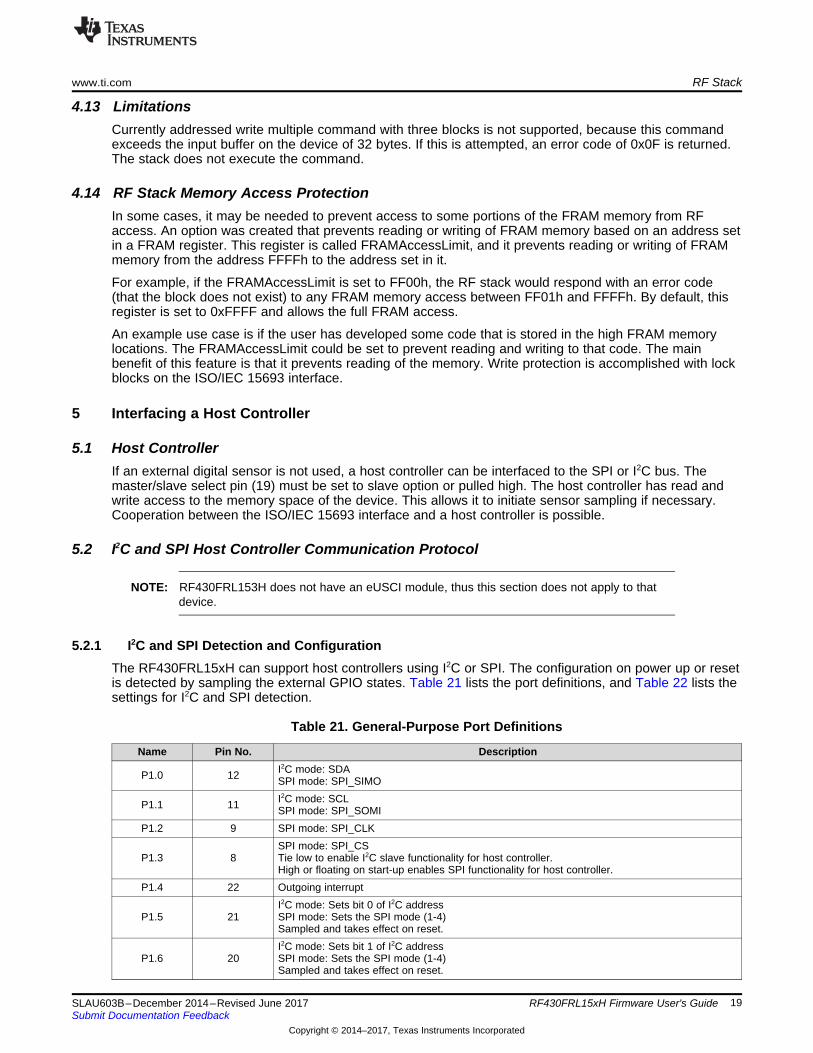
5.2.1 I2C and SPI Detection and ConfigurationThe RF430FRL15xH can support host controllers using I2C or SPI. The configuration on power up or resetis detected by sampling the external GPIO states. Table 21 lists the port definitions, and Table 22 lists thesettings for I2C and SPI detection.
Table 21. General-Purpose Port Definitions
Name Pin No. Description
P1.0 12 I2C mode: SDASPI mode: SPI_SIMO
P1.1 11 I2C mode: SCLSPI mode: SPI_SOMI
P1.2 9 SPI mode: SPI_CLK
P1.3 8SPI mode: SPI_CSTie low to enable I2C slave functionality for host controller.High or floating on start-up enables SPI functionality for host controller.
P1.4 22 Outgoing interrupt
P1.5 21I2C mode: Sets bit 0 of I2C addressSPI mode: Sets the SPI mode (1-4)Sampled and takes effect on reset.
P1.6 20I2C mode: Sets bit 1 of I2C addressSPI mode: Sets the SPI mode (1-4)Sampled and takes effect on reset.
Interfacing a Host Controller www.ti.com
20 SLAU603B–December 2014–Revised June 2017Submit Documentation Feedback
Copyright © 2014–2017, Texas Instruments Incorporated
RF430FRL15xH Firmware User's Guide
Table 21. General-Purpose Port Definitions (continued)Name Pin No. Description
P1.7 19Master or slave select for I2C or SPIConfigure low for master mode or high for slave mode (must have host controller).Sampled and takes effect on reset.
Table 22. I2C and SPI Detection
Pin No. Description High Low
19 Master or slave selectExternal host controller expected.
If host controller or digital sensor is not used,configure for this option.
Device in master I2C or SPI mode (expectsexternal digital sensor using serial bus)
8 I2C or SPI select(CS in SPI) If floating SPI bus is expected If grounded I2C bus is expected
20In I2C mode Bit 1 of I2C address is high Bit 1 of I2C address is lowIn SPI mode CPHA = 1 CPHA = 0
21In I2C mode Bit 0 of I2C address is high Bit 0 of I2C address is lowIn SPI mode CPOL = 1 CPOL = 0
5.3 I2C Host Controller Communication ProtocolA command is always initiated by the master by addressing the device using the specified I2C deviceaddress. The device address is a 7-bit I2C address with the upper 5 bits being hard-coded and the lower 2bit programmable by the input pins 20 and 21.
Table 23. I2C Device Address
Bit 6 Bit 5 Bit 4 Bit 3 Bit 2 Bit 1 Bit 00 1 1 0 0 Pin 20 Pin 21
5.3.1 I2C Write ProcedureTo write data, the device is addressed using the specified I2C device address with the R/W = 0 followed bythe upper 8 bits of the first address to be written and the lower 8 bits of that address. Immediately afterthat (without a repeated start) the data to be written starting at the specified address is received. Witheach data byte received the address is automatically incremented by one. The write access is terminatedby the STOP condition on the I2C bus.
www.ti.com Interfacing a Host Controller
21SLAU603B–December 2014–Revised June 2017Submit Documentation Feedback
Copyright © 2014–2017, Texas Instruments Incorporated
RF430FRL15xH Firmware User's Guide
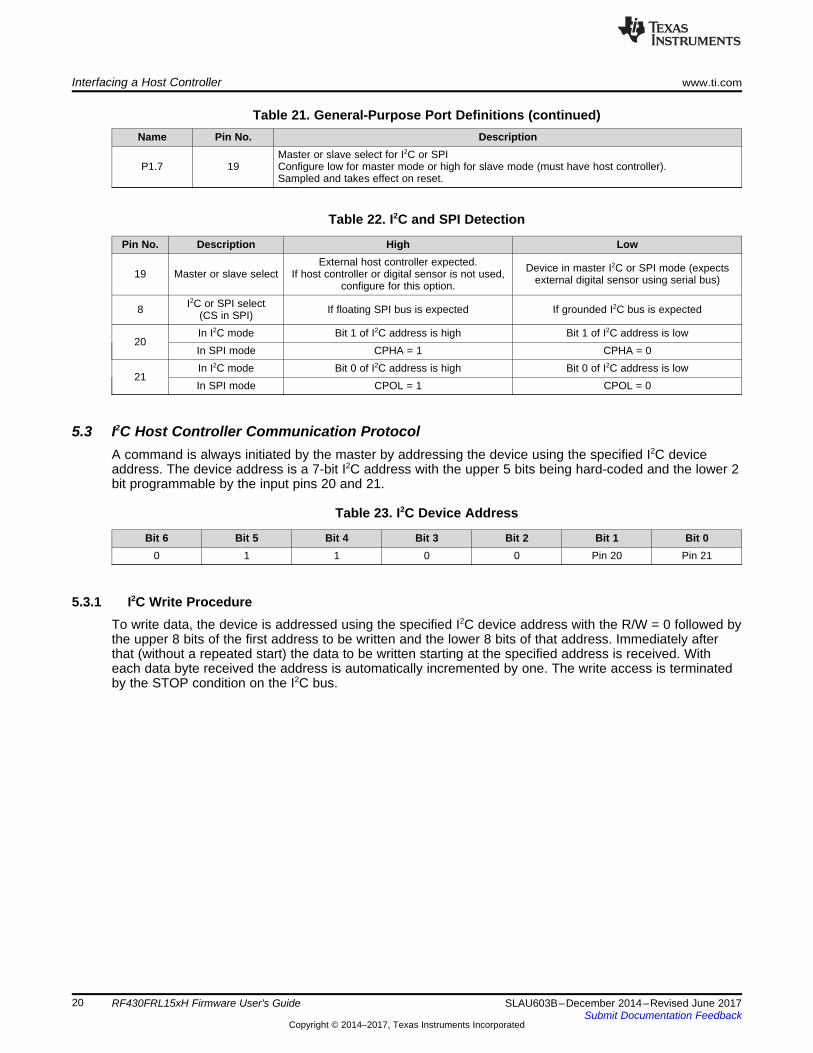
Figure 2. I2C Write Access
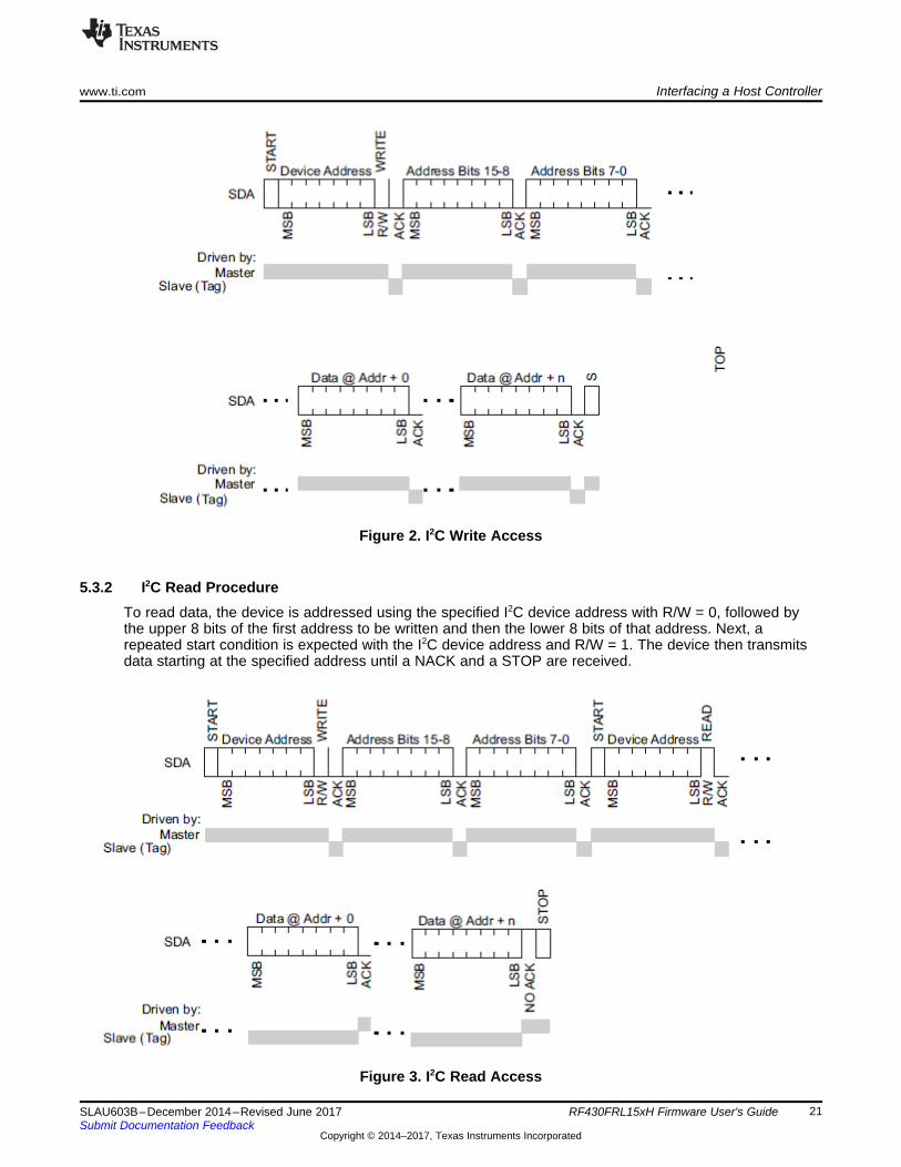
5.3.2 I2C Read ProcedureTo read data, the device is addressed using the specified I2C device address with R/W = 0, followed bythe upper 8 bits of the first address to be written and then the lower 8 bits of that address. Next, arepeated start condition is expected with the I2C device address and R/W = 1. The device then transmitsdata starting at the specified address until a NACK and a STOP are received.
Figure 3. I2C Read Access
Interfacing a Host Controller www.ti.com
22 SLAU603B–December 2014–Revised June 2017Submit Documentation Feedback
Copyright © 2014–2017, Texas Instruments Incorporated
RF430FRL15xH Firmware User's Guide
5.3.3 BIP-8 Communication Mode With I2CThe BIP-8 communication mode is enabled by setting the BIP-8 bit (BIP8Enable) in the control-statusregister. All communication after setting this bit uses the following conventions with exactly 2 addressbytes (16-bit address) and 2 data bytes (16-bit data).
5.3.3.1 I2C BIP8 Write
Table 24. Write Access
Master Address Bits15 to 8
Address Bits7 to 0
Data atAddress + 0
Data AtAddress + 1 BIP-8
Slave n/a n/a n/a n/a n/a
The Bit-Interleaved Parity (BIP-8) is calculated using 16-bit address and 16-bit data. If the received BIP-8does not match with received data no write is performed. (The BIP-8 calculation does not include the I2Cdevice address).
If a BIP-8 error is detected by the device, BIP8ErrorInt is set in the Status register, along with an interruptif enabled.
5.3.3.2 I2C BIP8 Read
Table 25. Read Access
Master Address 15 to 8 Address 7 to 0 n/a n/a n/aSlave n/a n/a Data at Addr + 0 Data at Addr + 1 BIP-8
For read access, the Bit-Interleaved Parity (BIP-8) is calculated using the received 16-bit address and the2 transmitted data bytes, and it is transmitted back to the master. The BIP-8 does not include the deviceaddress.
5.3.3.3 BIP-8 Calculation Pseudocode
uint8 BIP8 = 0;BIP8 ^= Address_15_to_8;BIP8 ^= Address_7_to_0;BIP8 ^= Data_0;BIP8 ^= Data_1;if (Write){
Send_packet_with_BIP8_Attached(BIP8);}else if (Read){
if (BIP8 == BIP8_Received){
//Correct BIP8, store the packetStore_Packet();
}else
{//Incorrect BIP8, indicates that there is an error in the packetDiscard_Packet();
}}
www.ti.com Interfacing a Host Controller
23SLAU603B–December 2014–Revised June 2017Submit Documentation Feedback
Copyright © 2014–2017, Texas Instruments Incorporated
RF430FRL15xH Firmware User's Guide
5.4 SPI Protocol
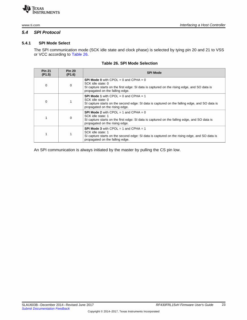
5.4.1 SPI Mode SelectThe SPI communication mode (SCK idle state and clock phase) is selected by tying pin 20 and 21 to VSSor VCC according to Table 26.
Table 26. SPI Mode Selection
Pin 21(P1.5)
Pin 20(P1.6) SPI Mode
0 0
SPI Mode 0 with CPOL = 0 and CPHA = 0SCK idle state: 0SI capture starts on the first edge: SI data is captured on the rising edge, and SO data ispropagated on the falling edge.
0 1
SPI Mode 1 with CPOL = 0 and CPHA = 1SCK idle state: 0SI capture starts on the second edge: SI data is captured on the falling edge, and SO data ispropagated on the rising edge.
1 0
SPI Mode 2 with CPOL = 1 and CPHA = 0SCK idle state: 1SI capture starts on the first edge: SI data is captured on the falling edge, and SO data ispropagated on the rising edge.
1 1
SPI Mode 3 with CPOL = 1 and CPHA = 1SCK idle state: 1SI capture starts on the second edge: SI data is captured on the rising edge, and SO data ispropagated on the falling edge.
An SPI communication is always initiated by the master by pulling the CS pin low.
Interfacing a Host Controller www.ti.com
24 SLAU603B–December 2014–Revised June 2017Submit Documentation Feedback
Copyright © 2014–2017, Texas Instruments Incorporated
RF430FRL15xH Firmware User's Guide
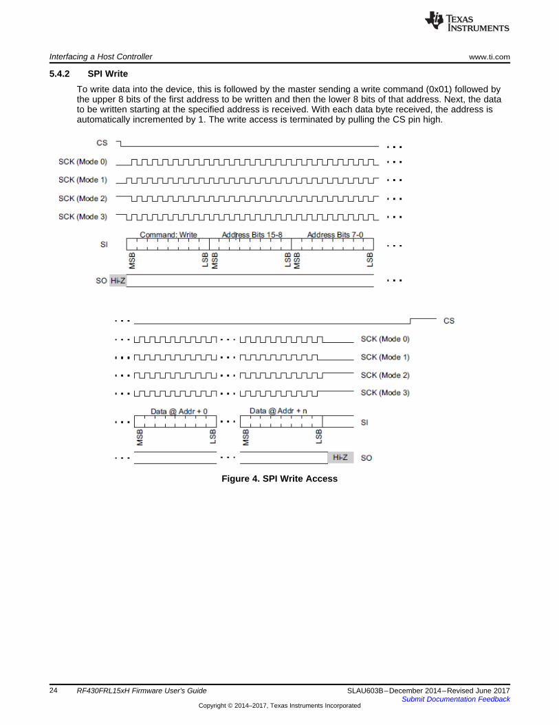
5.4.2 SPI WriteTo write data into the device, this is followed by the master sending a write command (0x01) followed bythe upper 8 bits of the first address to be written and then the lower 8 bits of that address. Next, the datato be written starting at the specified address is received. With each data byte received, the address isautomatically incremented by 1. The write access is terminated by pulling the CS pin high.
Figure 4. SPI Write Access
www.ti.com Interfacing a Host Controller
25SLAU603B–December 2014–Revised June 2017Submit Documentation Feedback
Copyright © 2014–2017, Texas Instruments Incorporated
RF430FRL15xH Firmware User's Guide
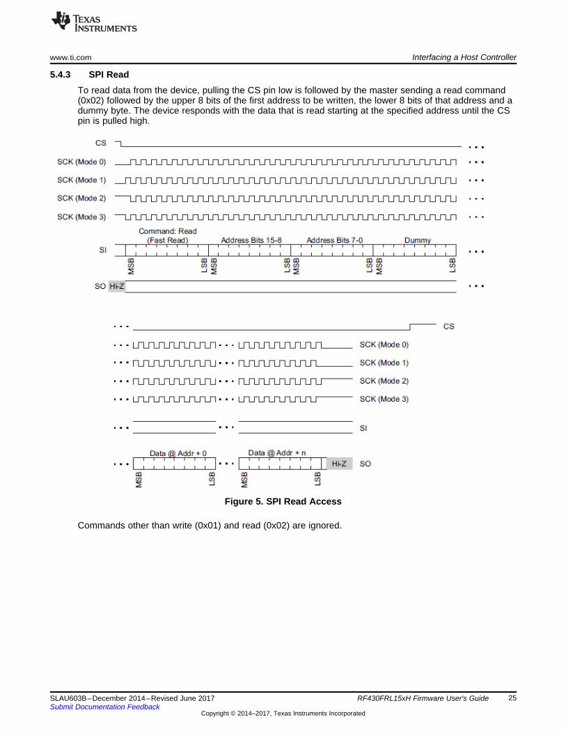
5.4.3 SPI ReadTo read data from the device, pulling the CS pin low is followed by the master sending a read command(0x02) followed by the upper 8 bits of the first address to be written, the lower 8 bits of that address and adummy byte. The device responds with the data that is read starting at the specified address until the CSpin is pulled high.
Figure 5. SPI Read Access
Commands other than write (0x01) and read (0x02) are ignored.
Interfacing a Host Controller www.ti.com
26 SLAU603B–December 2014–Revised June 2017Submit Documentation Feedback
Copyright © 2014–2017, Texas Instruments Incorporated
RF430FRL15xH Firmware User's Guide
5.4.4 BIP-8 Communication Mode With SPIThe BIP-8 communication mode is enabled by setting the BIP-8 bit (BIP8Enable) in the control-statusregister. All communication after setting this bit uses the following conventions with exactly 2 addressbytes (16-bit address) and 2 data bytes (16-bit data).
5.4.4.1 SPI BIP-8 WriteThe Bit-Interleaved Parity (BIP-8) is calculated using 16-bit address and 16-bit data. If the received BIP-8does not match with received data no write is performed. (The BIP-8 calculation does not include the writecommand byte.)
If a BIP-8 error is detected by the device, BIP8ErrorInt is set in the Status register, along with an interrupt,if enabled.
Table 27. Write Access
SI Command:Read Addr Bits 15 to 8 Addr Bits 7 to 0 Data at Addr + 0 Data at Addr + 1 BIP-8
SO n/a n/a n/a n/a n/a n/a
5.4.4.2 SPI BIP-8 ReadFor read access the Bit-Interleaved Parity (BIP-8) is calculated using the received 16-bit address, thereceived dummy byte and the 2 transmitted data bytes and transmitted back to the master. It does notinclude the read command byte or the "dummy" byte.
Table 28. Read Access
SI Command:Read
Address Bits15 to 8
Address Bits 7to 0 Dummy Byte n/a n/a n/a
SO n/a n/a n/a n/a Data at Addr + 0 Data at Addr + 1 BIP-8
5.5 Host Controller Memory Access RangeThe host controller can read the entire memory range of the device. However it is limited to what it canwrite to by default. To allow protected memory address write, the host controller has to set BusTestModefield in the control and status block to a high. This opens the capability to write to any memory of thedevice.
By default the writes are limited to the information in Table 29.
Table 29. Unprotected Memory Access Range
Low Range Access High Range AccessFRAM 0xF840 0xFFD0RAM 0x1E00 0x2C00
www.ti.com Interfacing a Host Controller
27SLAU603B–December 2014–Revised June 2017Submit Documentation Feedback
Copyright © 2014–2017, Texas Instruments Incorporated
RF430FRL15xH Firmware User's Guide
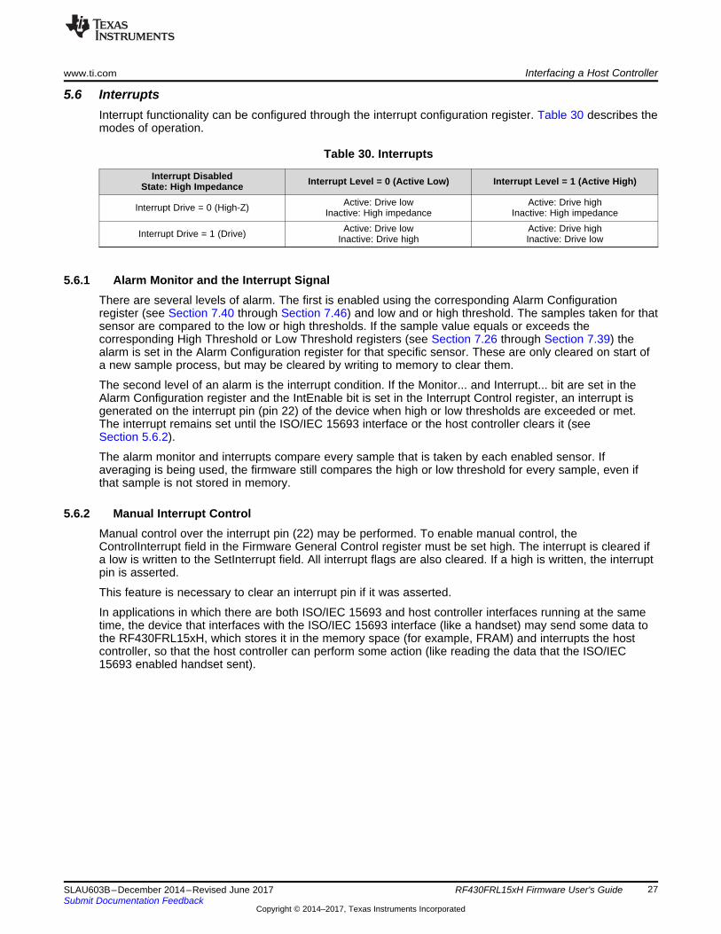
5.6 InterruptsInterrupt functionality can be configured through the interrupt configuration register. Table 30 describes themodes of operation.
Table 30. Interrupts
Interrupt DisabledState: High Impedance Interrupt Level = 0 (Active Low) Interrupt Level = 1 (Active High)
Interrupt Drive = 0 (High-Z) Active: Drive lowInactive: High impedance
Active: Drive highInactive: High impedance
Interrupt Drive = 1 (Drive) Active: Drive lowInactive: Drive high
Active: Drive highInactive: Drive low
5.6.1 Alarm Monitor and the Interrupt SignalThere are several levels of alarm. The first is enabled using the corresponding Alarm Configurationregister (see Section 7.40 through Section 7.46) and low and or high threshold. The samples taken for thatsensor are compared to the low or high thresholds. If the sample value equals or exceeds thecorresponding High Threshold or Low Threshold registers (see Section 7.26 through Section 7.39) thealarm is set in the Alarm Configuration register for that specific sensor. These are only cleared on start ofa new sample process, but may be cleared by writing to memory to clear them.
The second level of an alarm is the interrupt condition. If the Monitor... and Interrupt... bit are set in theAlarm Configuration register and the IntEnable bit is set in the Interrupt Control register, an interrupt isgenerated on the interrupt pin (pin 22) of the device when high or low thresholds are exceeded or met.The interrupt remains set until the ISO/IEC 15693 interface or the host controller clears it (seeSection 5.6.2).
The alarm monitor and interrupts compare every sample that is taken by each enabled sensor. Ifaveraging is being used, the firmware still compares the high or low threshold for every sample, even ifthat sample is not stored in memory.
5.6.2 Manual Interrupt ControlManual control over the interrupt pin (22) may be performed. To enable manual control, theControlInterrupt field in the Firmware General Control register must be set high. The interrupt is cleared ifa low is written to the SetInterrupt field. All interrupt flags are also cleared. If a high is written, the interruptpin is asserted.
This feature is necessary to clear an interrupt pin if it was asserted.
In applications in which there are both ISO/IEC 15693 and host controller interfaces running at the sametime, the device that interfaces with the ISO/IEC 15693 interface (like a handset) may send some data tothe RF430FRL15xH, which stores it in the memory space (for example, FRAM) and interrupts the hostcontroller, so that the host controller can perform some action (like reading the data that the ISO/IEC15693 enabled handset sent).
Example Projects www.ti.com
28 SLAU603B–December 2014–Revised June 2017Submit Documentation Feedback
Copyright © 2014–2017, Texas Instruments Incorporated
RF430FRL15xH Firmware User's Guide
6 Example Projects
6.1 Blank ProjectIn this case, no ROM firmware is used. What determines that no ROM firmware is used is that all of theinterrupt vectors, reset, RF13M, eUSCI, and other features are all programmed to point to functions thatthe user creates in FRAM. The interrupt vectors are located at the last memory locations in FRAM.
With this configuration, the user is free to create a custom functioning device. The only limitation is thatthe whole program must fit into the FRAM memory (2KB). Also the energy use is a little more than runningfrom ROM.
There are no example projects provided for this case as it is expected that the user creates theapplication.
6.2 ISO/IEC 15693 RF Stack (NFC) OnlyIn this mode, the only part of the ROM that is used is the RF stack. The user is free to create a customprogram that does not follow the application presented in this user guide.
Some parts of the RAM are reserved for ROM code access and cannot be used by the user. The RFstack allows RF access to most of the FRAM memory.
In this mode, it is possible to use the device in NDEF format, because with the main application disabled,all of the virtual registers that exist in the first blocks of FRAM are not used. Therefore, it is possible toplace the NFC capability container and the message there instead.
Host controller ROM support is not available in this project. If that is needed, perhaps the user shouldconsider the default project.
Example RF stack only projects are provided online for each device variant.
Table 31. Memory Reserved in RF Stack Only Project
Label Address CommentISO/IEC 15693 F848h-F866h This memory is reserved for ISO/IEC 15693 lock block tracking
System FirmwareControl Register F867h
ROM_SENSOR_SUPPORT_DISABLED – no ROM support for ADCROM_EUSCI_SUPPORT_DISABLE - no host controller ROM support possible in thisprojectEIGHT_BYTE_BLOCK – this can be changed to 4 byte block optionFIRST_ISO_PAGE – because 8 byte block option is used, this is "do not care".
NDEF Space("FRAM") F868h-FCD0h
The range on this memory allocation is arbitrary, depending on where the nextsegment of FRAM begins. This segment may be used for NDEF message storing orother purposes.
FRAM Code FCD0-FFFF
This segment of memory is allocated to storing any custom code in FRAM. Again thefirst memory segment must start at F868h and the next one end at 0xFFFF. Thedivision in the middle is arbitrary. If these two memory segments lengths must bechanged, change them in the lnk_rf430frl15xh_NFC_Only.cmd file.
RAM variable Various RAMlocations
There are some RAM locations that are reserved in the NFC only projects. There isnothing the user needs to do except keep the "ROM Variables" section unchanged.
6.3 External Digital Sensor Driver Firmware (Sensor Hub BoosterPack)An external digital sensor may be interfaced to the device. It may have an SPI or I2C interface. There is noROM code on the part to handle any specific device as it is expected that the code is programmed to theFRAM. The device forwards execution to the FRAM to sample the digital sensor (assuming it is enabled).The code in FRAM is executed, and it is expected to store a value in a mailbox that is used by the ROMfirmware for processing and storing the data. A sample application has been created to support the sensorhub booster pack. It can be found in the RF430FRL152HEVM product folder(www.ti.com/tool/RF430FRL152HEVM) in the "Software" section.
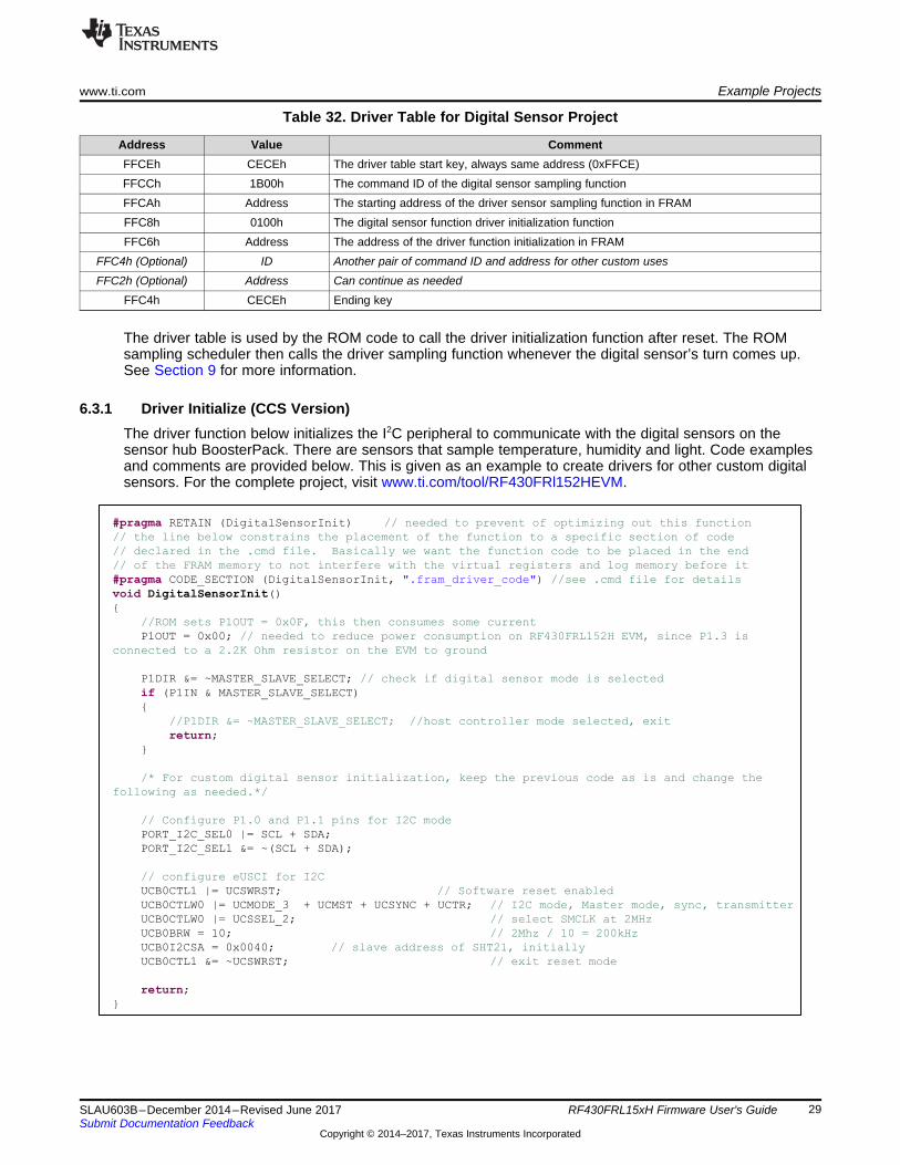
#pragma RETAIN (DigitalSensorInit) // needed to prevent of optimizing out this function
// the line below constrains the placement of the function to a specific section of code
// declared in the .cmd file. Basically we want the function code to be placed in the end
// of the FRAM memory to not interfere with the virtual registers and log memory before it
#pragma CODE_SECTION (DigitalSensorInit, ".fram_driver_code") //see .cmd file for details
void DigitalSensorInit()
{
//ROM sets P1OUT = 0x0F, this then consumes some current
P1OUT = 0x00; // needed to reduce power consumption on RF430FRL152H EVM, since P1.3 is
connected to a 2.2K Ohm resistor on the EVM to ground
P1DIR &= ~MASTER_SLAVE_SELECT; // check if digital sensor mode is selected
if (P1IN & MASTER_SLAVE_SELECT)
{
//P1DIR &= ~MASTER_SLAVE_SELECT; //host controller mode selected, exit
return;
}
/* For custom digital sensor initialization, keep the previous code as is and change the
following as needed.*/
// Configure P1.0 and P1.1 pins for I2C mode
PORT_I2C_SEL0 |= SCL + SDA;
PORT_I2C_SEL1 &= ~(SCL + SDA);
// configure eUSCI for I2C
UCB0CTL1 |= UCSWRST; // Software reset enabled
UCB0CTLW0 |= UCMODE_3 + UCMST + UCSYNC + UCTR; // I2C mode, Master mode, sync, transmitter
UCB0CTLW0 |= UCSSEL_2; // select SMCLK at 2MHz
UCB0BRW = 10; // 2Mhz / 10 = 200kHz
UCB0I2CSA = 0x0040; // slave address of SHT21, initially
UCB0CTL1 &= ~UCSWRST; // exit reset mode
return;
}
www.ti.com Example Projects
29SLAU603B–December 2014–Revised June 2017Submit Documentation Feedback
Copyright © 2014–2017, Texas Instruments Incorporated
RF430FRL15xH Firmware User's Guide
Table 32. Driver Table for Digital Sensor Project
Address Value CommentFFCEh CECEh The driver table start key, always same address (0xFFCE)FFCCh 1B00h The command ID of the digital sensor sampling functionFFCAh Address The starting address of the driver sensor sampling function in FRAMFFC8h 0100h The digital sensor function driver initialization functionFFC6h Address The address of the driver function initialization in FRAM
FFC4h (Optional) ID Another pair of command ID and address for other custom usesFFC2h (Optional) Address Can continue as needed
FFC4h CECEh Ending key
The driver table is used by the ROM code to call the driver initialization function after reset. The ROMsampling scheduler then calls the driver sampling function whenever the digital sensor’s turn comes up.See Section 9 for more information.
6.3.1 Driver Initialize (CCS Version)The driver function below initializes the I2C peripheral to communicate with the digital sensors on thesensor hub BoosterPack. There are sensors that sample temperature, humidity and light. Code examplesand comments are provided below. This is given as an example to create drivers for other custom digitalsensors. For the complete project, visit www.ti.com/tool/RF430FRl152HEVM.

// location digital sensor measurement is to be placed in for the ROM code to use it
#define RESULT_MAILBOX *((u16_t *)0x1D02)
// ROM code sets this address to the current digital sensor to be sampled
#define SENSOR_TYPE_MAILBOX *((u16_t *)0x1D04)
#pragma RETAIN (DigitalSensorMeasurement) // needed to prevent of optimizing out this function
// the line below constrains the placement of the function to a specific section of code
// declared in the .cmd file. Basically we want the function code to be placed in the end
// of the FRAM memory to not interfere with the virtual registers and log memory before it
#pragma CODE_SECTION (DigitalSensorMeasurement, ".fram_driver_code")//see .cmd file for
details
u08_t DigitalSensorMeasurement ()
{
u08_t temp_data[2]; // used for temporary data and the 16-bit data that is sampled
u08_t sensor_sampled = 0;// flag to keep track if any sensor was actually sampled
// does the ROM code request digital sensor 1 (SHT21 temperature) to be sampled?
if (SENSOR_TYPE_MAILBOX == DIGITAL_SENSOR1)
{
/* To add processing for custom digital sensor 1:
* Collect data over I2C
* Add lines below to send data to ROM application
* RESULT_MAILBOX = (u16_t)temp_data[1] + (((u16_t)(temp_data[0])) << 8);
* store the result in the mailbox so that the ROM code will use it
* sensor_read = 1;
// sensor read was performed
*
* If this digital sensor is not needed use only line below in this block
* sensor_read = 0
*/
/*********** Sensor Hub Boosterpack SHT21 temperature measurement ************************/
// take the temperature measurement over I2C
SHT_21_I2C_Master_Measurement(TEMP_MEASURE_HOLD_MASTER, temp_data);
// store the result in the mailbox so that the ROM code will use it
RESULT_MAILBOX = (u16_t)temp_data[1] + (((u16_t)(temp_data[0])) << 8);
sensor_sampled= 1;
// sensor sampling was performed
}
// does the ROM code request digital sensor 2 (SHT21 humidity) to be sampled?
else if(SENSOR_TYPE_MAILBOX == DIGITAL_SENSOR2) {
sensor_sampled= 0; // this sensor is not needed and therefore was not sampled
}
// does the ROM code request digital sensor 3 (ISL29023 light) to be sampled?
else if(SENSOR_TYPE_MAILBOX == DIGITAL_SENSOR3) {
// more code
}
return sensor_sampled
// indicates that a sensor read was performed, the ROM code will only store the value on a
non-zero result here
}
Example Projects www.ti.com
30 SLAU603B–December 2014–Revised June 2017Submit Documentation Feedback
Copyright © 2014–2017, Texas Instruments Incorporated
RF430FRL15xH Firmware User's Guide
6.3.2 Sensor Sample Driver (CCS Version)The scheduler in the ROM determines when the selected digital sensor sampling turn comes up. When itdoes, it calls the following function. It provides a number for which digital sensor is to be sampled. This isnecessary because this one function has to handle the sampling of the three digital sensors possible bythe device.
After the sample has occurred, this function returns the result to the "mailbox" that the ROM code uses tocollect the result and do some processing on it (for example, threshold checking) before storing it.
www.ti.com Registers
31SLAU603B–December 2014–Revised June 2017Submit Documentation Feedback
Copyright © 2014–2017, Texas Instruments Incorporated
RF430FRL15xH Firmware User's Guide
6.3.3 Mailbox Variables For Implementing Digital Sensor DriverSeveral mailboxes are available to pass information between the ROM code and code that has beenadded in the FRAM.
Table 33. Mailbox Table for Digital Sensor Project
Name Address Length Comment
Result Mailbox 1D02h unsigned 16-bit The digital sensor sample result is written to this memory location inRAM.
Sensor Type Mailbox 1D04h unsigned 16-bit ROM code sets this address to the current digital sensor to be sampled
Function return unsigned 8-bit Non-zero value results in the value written to result mailbox to be loggedby the ROM code.
7 RegistersFor the host controller, execution (like software reset, sensor sampling process, or manually changing theinterrupt pin) is initiated only when the control register is written. It is suggested to set this register last inthe configuration procedure, so that further memory access does not occur when the device is samplingsensors.
7.1 Reading the Register Address BarAll the following registers are present on this device.
The following sections describe virtual registers that are present on the device in FRAM. The address baris given for every register.
To make sure there are not any confusion, the address bar definition is provided below. The examplebelow is for a register called "ADC0 Sensor Configuration", however this definition can be applied to allother registers.
Memory Type Address ISO 8-Byte Blk No. 4-Byte Blk No. -Page Byte No. 8/4-Byte
FRAM F87Ah 2 4-0 2-2
ADC0 Sensor Configuration
Address Register Name
F877h ***
F878h ***
F879h ***
F87Ah ADCO Sen. Cfg.
F87Bh ***
F87Ch ***
F87Dh ***
F87Eh ***
F87Fh ***
8-Byte
Block No.
8-Byte
Byte No.
1 7
2 0
2 1
2 2
2 3
2 4
2 5
2 6
2 7
4-Byte
Block No.
4-Byte
Byte No.
3 3
4 0
4 1
4 2
4 3
5 0
5 1
5 2
5 3
F880h *** 3 0 6 0
Registers www.ti.com
32 SLAU603B–December 2014–Revised June 2017Submit Documentation Feedback
Copyright © 2014–2017, Texas Instruments Incorporated
RF430FRL15xH Firmware User's Guide
Figure 6. Address Bar Definition
7.2 Firmware General Control RegisterIf a reset value is provided to any of the registers, it is set only if the FRAM Data Valid register is notinitialized to a particular value (see Section 7.50). If the FRAM Data Valid has been initialized correctly,then the variables are not reset. The FRAM Data Valid register is initialized on reset only when it does notmatch the expected reset value.
NOTE: The FRAM memory space is initialized to ones after manufacturing. The FRAM interruptvectors are set to the correct value when the reset vector is detected to be 0xFFFF.

www.ti.com Registers
33SLAU603B–December 2014–Revised June 2017Submit Documentation Feedback
Copyright © 2014–2017, Texas Instruments Incorporated
RF430FRL15xH Firmware User's Guide
Table 34. General Control Register
Memory Type Address ISO 8-Byte Blk No. 4-Byte Blk No. - Page Byte No. 8/4-ByteFRAM F868h 0 0-0 0-0
Table 35. General Control Register Description
Bit Field Name Type Reset Field Description
0 Start R/W 0
Writing to this register and setting this bit high always starts anew sampling process. If sampling is already in progress,unspecified operation occurs.To terminate this process, set the Reset bit.Fifth in action priority for this register.
1 PowerMode R/W 0
Changing these settings will cause entering of the selectedpower in idle mode0 = Default power mode (LPM3)1 = LPM4
2 ControlPower R/W 0 High enables battery switch control (next field).Third in action priority.
3 SetPower R/W 0 Sets the battery switch state if the Control Power bit is set.4 Reserved R 0 Only write 0 to this register
5 ControlInterrupt R/W 0 Enable the control of the SetInterrupt field.Second in action priority for this register.
6 SetInterrupt R/W 0Set the interrupt pin through this field.High asserts the interrupt, low clears the interrupt and interruptflags.
7 Reset R/W 0 High initiates a software reset.First in action priority for this register.
7.3 Firmware Status RegisterThis register is not protected from writes using I2C or SPI. It is protected using the RF interface.
Table 36. Status Register
Memory Type Address ISO 8-Byte Blk No. 4-Byte Blk No. - Page Byte No. 8/4-ByteFRAM F869h 0 0-0 1-1
Table 37. Status Register Description
Bit Field Name Type Reset Field Description
1:0 State R 0
0 = Idle state1 = Sampling in progress2 = Data available in FRAM3 = An error has occurred with the last sampling processReset when there is a new sample request
2 Overflow R 00 = No overflow1 = FRAM memory overflow has occurred (reset after newsample request)
3 Timing Error R 0 0 = No timing error1 = Timing error has occurred (reset after new sample request)
4 EndOfSampleInt R 0 High indicates that a sampling process has completed
5 BIP8ErrorInt R 0 Host Controller Control FieldHigh indicates that there was a BIP-8 error using BIP-8 mode
6 NFCBridgeRXInt R 0 High indicates that ISO/IEC 15693 data has been received andin direct mode.
7 ThresholdInterrupt R 0 High indicates that a threshold (high or low) has been exceeded.Read all.
Registers www.ti.com
34 SLAU603B–December 2014–Revised June 2017Submit Documentation Feedback
Copyright © 2014–2017, Texas Instruments Incorporated
RF430FRL15xH Firmware User's Guide
7.4 Sensor Control Register
Table 38. Sensor Control Register
Memory Type Address ISO 8-Byte Blk No. 4-Byte Blk No. - Page Byte No. 8/4-ByteFRAM F86Ah 0 0-0 2-2
Table 39. Sensor Control Register Description
Bit Field Name Type Reset Field Description0 ReferenceADC1Sensor R/W 0 High enables this sensor to sample
1 ThermistorADC2Sensor R/W 0High enables this sensor to sampleSetting this bit causes ADC1 and ADC2 samples to beskipped.
2 ADC0Sensor R/W 0 High enables this sensor to sample3 InternalSensor R/W 0 High enables this sensor to sample4 DigitalSensor1 R/W 0 High enables this sensor to sample5 DigitalSensor2 R/W 0 High enables this sensor to sample6 DigitalSensor2 R/W 0 High enables this sensor to sample7 Reserved R/W 0 Do not use
7.5 Frequency Register
Table 40. Frequency Register
Memory Type Address ISO 8-Byte Blk No. 4-Byte Blk No. - Page Byte No. 8/4-ByteFRAM F86Bh 0 0-0 3-3
Table 41. Frequency Register Description
Bit Field Name Type Reset Field Description
4:0 Frequency R/W 3
0 = Four times per second1 = Two times per second2 = Every second3 = Every five seconds4 = Every fifteen seconds5 = Every thirty seconds6 = Every minute7 = Every two minutes8 = Every five minutes9 = Every ten minutes10 = Every thirty minutes11 = Every hour12 = Every two hours13 = Every five hours14 = Every ten hours15 = Every twenty four hours16 = Custom time (set in Custom Timer Value register)Anyother setting will default to every 5 seconds period
7:5 NumberOfPasses10_8 R/W 0These are the most significant bits of the Number of Passesfield (11 bits long). The least significant bits are set in theNumber of Passes register (Section 7.6).
www.ti.com Registers
35SLAU603B–December 2014–Revised June 2017Submit Documentation Feedback
Copyright © 2014–2017, Texas Instruments Incorporated
RF430FRL15xH Firmware User's Guide
7.6 Number of Passes Register
Table 42. Number of Passes Register
Memory Type Address ISO 8-Byte Blk No. 4-Byte Blk No. - Page Byte No. 8/4-ByteFRAM F86Ch 0 1-0 4-0
Table 43. Number of Passes Register Description
Bit Field Name Type Reset Field Description
7:0 NumberOfPasses7_0 R/W 0
Number of passes to make through the selected sensors(configured in the Sensor Control register [Section 7.4)] [themost significant bits of this value is in the FrequencyRegister (Section 7.5)]
7.7 Averaging Register
Table 44. Averaging Register
Memory Type Address ISO 8-Byte Blk No. 4-Byte Blk No. - Page Byte No. 8/4-ByteFRAM F86Dh 0 1-0 5-1
Table 45. Averaging Register Description
Bit Field Name Type Reset Field Description
7:0 AveragingSamples R/W 1
Number of samples to average Range is from 1-255Writing 1 results in no averaging. Anything greater than 1causes that many samples to be temporarily stored and thenaveraged. At that time, the averaged value is stored. Thisregister also controls peak store and sampling.
Registers www.ti.com
36 SLAU603B–December 2014–Revised June 2017Submit Documentation Feedback
Copyright © 2014–2017, Texas Instruments Incorporated
RF430FRL15xH Firmware User's Guide
7.8 Interrupt Control Register
Table 46. Interrupt Control Register
Memory Type Address ISO 8-Byte Blk No. 4-Byte Blk No. - Page Byte No. 8/4-ByteFRAM F86Eh 0 1-0 6-2
Table 47. Interrupt Control Register Description
Bit Field Name Type Reset Field Description
0 Infinite Sampling R/W 0Setting this bit causes sampling to occur without an endtime. To stop clear the Start bit. Number of Passes registermust be set to 2.
1 InterruptLevel R/W 0Interrupt output pin configuration0 = Interrupts are signaled with an active low.1 = Interrupts are signaled with an active high.
2 InterruptDrive R/W 0
Interrupt Output pin Interrupt Configuration0b – Pin is Hi-Z if there is no pending interrupt. Applicationprovides an external pull-up resistor if bit 3 (Interrupt ActiveHigh) = 0. Application provides an external pull-downresistor if bit 3 (INTO Active High) = 1.1b – Pin is actively driven high or low if there is no pendinginterrupt: it is driven high if bit 3 (INTO Active High) = 0; it isdriven low if bit 3 (INTO Active High) = 1.
3 InterruptEnable R/W 0 Enables the interrupt functionality
4 EndOfSampleIntEn R/W 00 = No interrupt is set at the end of the sample process1 = Interrupt is asserted at the end of the sensor sampleprocess, if this is set high.
5 ShutDownOnSampleEnd R/W 0
0 = After end of sample collection, device goes into lowpower mode1 = Open the battery switch at the end of the sensor sampleprocess
6 CheckResetError R/W 0 Checks reset errors on power up and logs them at end ofdata FRAM
7 BIP8IntEn R/W 0 Host Controller Control FieldHigh enables BIP-8 interrupt
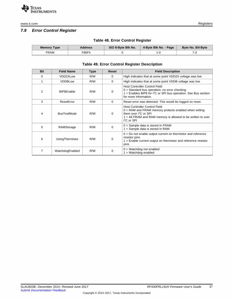
www.ti.com Registers
37SLAU603B–December 2014–Revised June 2017Submit Documentation Feedback
Copyright © 2014–2017, Texas Instruments Incorporated
RF430FRL15xH Firmware User's Guide
7.9 Error Control Register
Table 48. Error Control Register
Memory Type Address ISO 8-Byte Blk No. 4-Byte Blk No. - Page Byte No. 8/4-ByteFRAM F86Fh 0 1-0 7-3
Table 49. Error Control Register Description
Bit Field Name Type Reset Field Description0 VDD2XLow R/W 0 High indicates that at some point VDD2X voltage was low1 VDDBLow R/W 0 High indicates that at some point VDDB voltage was low
2 BIP8Enable R/W 0
Host Controller Control Field0 = Standard bus operation, no error checking1 = Enables BIP8 for I2C or SPI bus operation. See Bus sectionfor more information.
3 ResetError R/W 0 Reset error was detected. This would be logged on reset.
4 BusTestMode R/W 0
Host Controller Control Field0 = RAM and FRAM memory protects enabled when writingthem over I2C or SPI1 = All FRAM and RAM memory is allowed to be written to overI2C or SPI
5 RAMStorage R/W 0 0 = Sample data is stored in FRAM1 = Sample data is stored in RAM
6 UsingThermistor R/W 0
0 = Do not enable output current on thermistor and referenceresistor pins1 = Enable current output on thermistor and reference resistorpins
7 WatchdogEnabled R/W 0 0 = Watchdog not enabled1 = Watchdog enabled
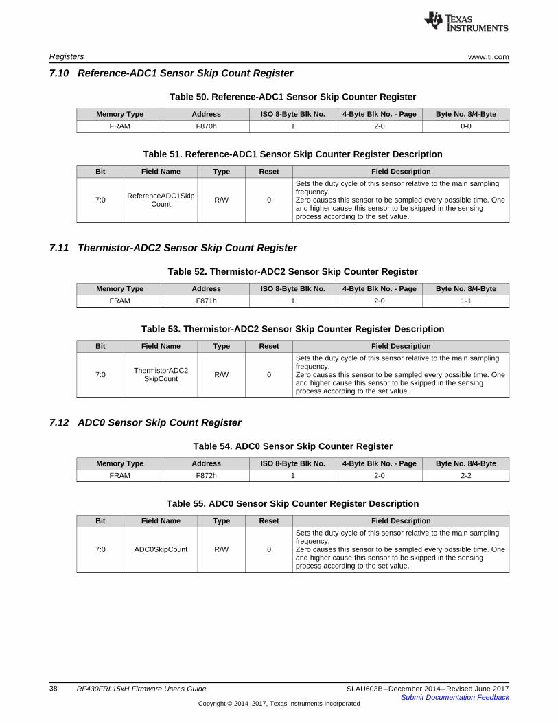
Registers www.ti.com
38 SLAU603B–December 2014–Revised June 2017Submit Documentation Feedback
Copyright © 2014–2017, Texas Instruments Incorporated
RF430FRL15xH Firmware User's Guide
7.10 Reference-ADC1 Sensor Skip Count Register
Table 50. Reference-ADC1 Sensor Skip Counter Register
Memory Type Address ISO 8-Byte Blk No. 4-Byte Blk No. - Page Byte No. 8/4-ByteFRAM F870h 1 2-0 0-0
Table 51. Reference-ADC1 Sensor Skip Counter Register Description
Bit Field Name Type Reset Field Description
7:0 ReferenceADC1SkipCount R/W 0
Sets the duty cycle of this sensor relative to the main samplingfrequency.Zero causes this sensor to be sampled every possible time. Oneand higher cause this sensor to be skipped in the sensingprocess according to the set value.
7.11 Thermistor-ADC2 Sensor Skip Count Register
Table 52. Thermistor-ADC2 Sensor Skip Counter Register
Memory Type Address ISO 8-Byte Blk No. 4-Byte Blk No. - Page Byte No. 8/4-ByteFRAM F871h 1 2-0 1-1
Table 53. Thermistor-ADC2 Sensor Skip Counter Register Description
Bit Field Name Type Reset Field Description
7:0 ThermistorADC2SkipCount R/W 0
Sets the duty cycle of this sensor relative to the main samplingfrequency.Zero causes this sensor to be sampled every possible time. Oneand higher cause this sensor to be skipped in the sensingprocess according to the set value.
7.12 ADC0 Sensor Skip Count Register
Table 54. ADC0 Sensor Skip Counter Register
Memory Type Address ISO 8-Byte Blk No. 4-Byte Blk No. - Page Byte No. 8/4-ByteFRAM F872h 1 2-0 2-2
Table 55. ADC0 Sensor Skip Counter Register Description
Bit Field Name Type Reset Field Description
7:0 ADC0SkipCount R/W 0
Sets the duty cycle of this sensor relative to the main samplingfrequency.Zero causes this sensor to be sampled every possible time. Oneand higher cause this sensor to be skipped in the sensingprocess according to the set value.
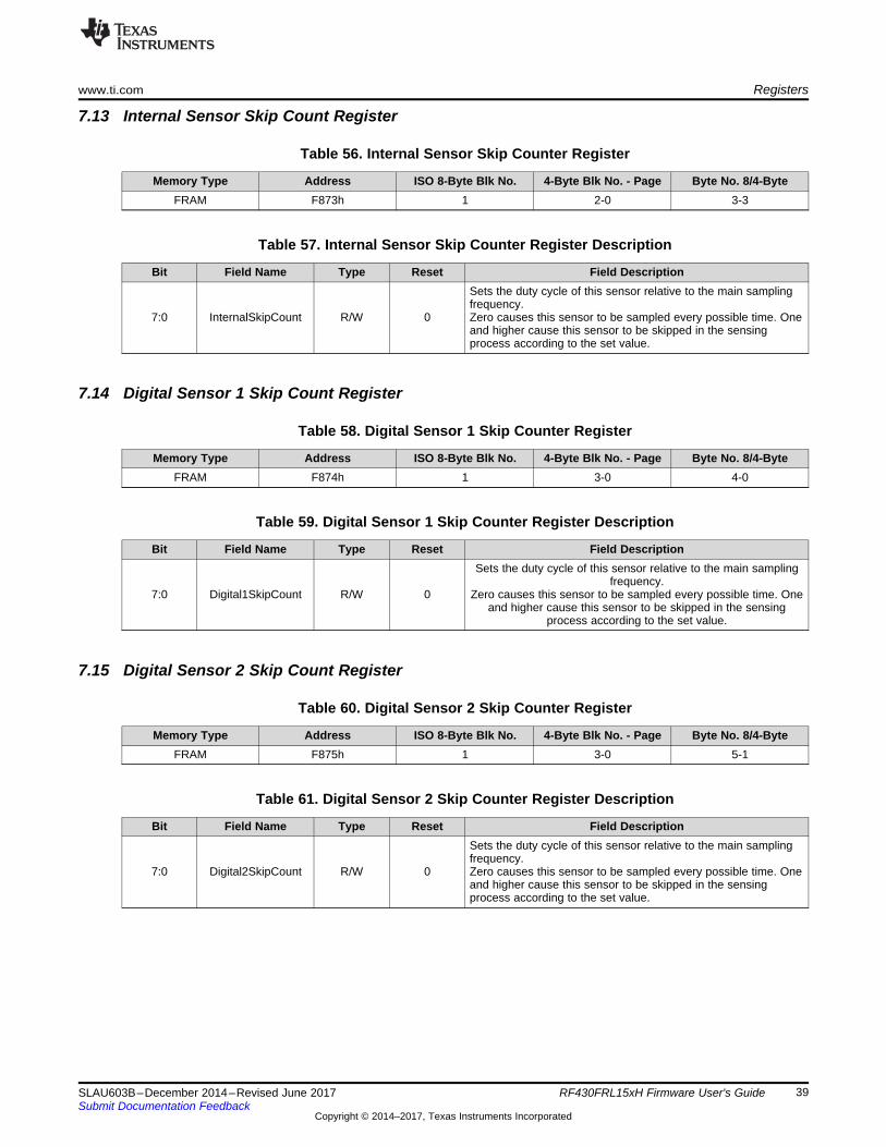
www.ti.com Registers
39SLAU603B–December 2014–Revised June 2017Submit Documentation Feedback
Copyright © 2014–2017, Texas Instruments Incorporated
RF430FRL15xH Firmware User's Guide
7.13 Internal Sensor Skip Count Register
Table 56. Internal Sensor Skip Counter Register
Memory Type Address ISO 8-Byte Blk No. 4-Byte Blk No. - Page Byte No. 8/4-ByteFRAM F873h 1 2-0 3-3
Table 57. Internal Sensor Skip Counter Register Description
Bit Field Name Type Reset Field Description
7:0 InternalSkipCount R/W 0
Sets the duty cycle of this sensor relative to the main samplingfrequency.Zero causes this sensor to be sampled every possible time. Oneand higher cause this sensor to be skipped in the sensingprocess according to the set value.
7.14 Digital Sensor 1 Skip Count Register
Table 58. Digital Sensor 1 Skip Counter Register
Memory Type Address ISO 8-Byte Blk No. 4-Byte Blk No. - Page Byte No. 8/4-ByteFRAM F874h 1 3-0 4-0
Table 59. Digital Sensor 1 Skip Counter Register Description
Bit Field Name Type Reset Field Description
7:0 Digital1SkipCount R/W 0
Sets the duty cycle of this sensor relative to the main samplingfrequency.
Zero causes this sensor to be sampled every possible time. Oneand higher cause this sensor to be skipped in the sensing
process according to the set value.
7.15 Digital Sensor 2 Skip Count Register
Table 60. Digital Sensor 2 Skip Counter Register
Memory Type Address ISO 8-Byte Blk No. 4-Byte Blk No. - Page Byte No. 8/4-ByteFRAM F875h 1 3-0 5-1
Table 61. Digital Sensor 2 Skip Counter Register Description
Bit Field Name Type Reset Field Description
7:0 Digital2SkipCount R/W 0
Sets the duty cycle of this sensor relative to the main samplingfrequency.Zero causes this sensor to be sampled every possible time. Oneand higher cause this sensor to be skipped in the sensingprocess according to the set value.
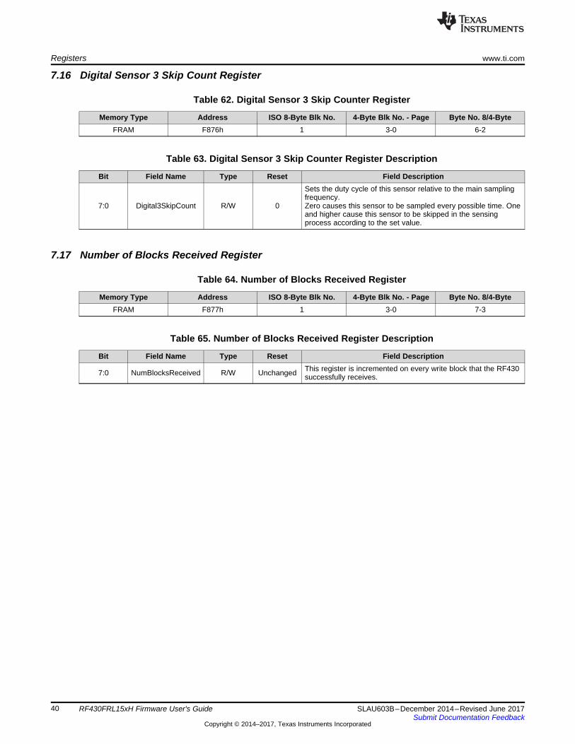
Registers www.ti.com
40 SLAU603B–December 2014–Revised June 2017Submit Documentation Feedback
Copyright © 2014–2017, Texas Instruments Incorporated
RF430FRL15xH Firmware User's Guide
7.16 Digital Sensor 3 Skip Count Register
Table 62. Digital Sensor 3 Skip Counter Register
Memory Type Address ISO 8-Byte Blk No. 4-Byte Blk No. - Page Byte No. 8/4-ByteFRAM F876h 1 3-0 6-2
Table 63. Digital Sensor 3 Skip Counter Register Description
Bit Field Name Type Reset Field Description
7:0 Digital3SkipCount R/W 0
Sets the duty cycle of this sensor relative to the main samplingfrequency.Zero causes this sensor to be sampled every possible time. Oneand higher cause this sensor to be skipped in the sensingprocess according to the set value.
7.17 Number of Blocks Received Register
Table 64. Number of Blocks Received Register
Memory Type Address ISO 8-Byte Blk No. 4-Byte Blk No. - Page Byte No. 8/4-ByteFRAM F877h 1 3-0 7-3
Table 65. Number of Blocks Received Register Description
Bit Field Name Type Reset Field Description
7:0 NumBlocksReceived R/W Unchanged This register is incremented on every write block that the RF430successfully receives.

www.ti.com Registers
41SLAU603B–December 2014–Revised June 2017Submit Documentation Feedback
Copyright © 2014–2017, Texas Instruments Incorporated
RF430FRL15xH Firmware User's Guide
7.18 Reference-ADC1 Configuration Register
Table 66. Reference-ADC1 Configuration Register
Memory Type Address ISO 8-Byte Blk No. 4-Byte Blk No. - Page Byte No. 8/4-ByteFRAM F878h 2 4-0 0-0
Table 67. Reference-ADC1 Configuration Register Description
Bit Field Name Type Reset Field Description
1:0 SensorGainThermADC1 R/W 1
0 = Gain of 11 = Gain of 22 = Gain of 43 = Gain of 8
2 FilterTypeTherm ADC1 R/W 0 0 = CIC Filter1 = Moving Average Filter
5:3 OversamplingRateThermADC1 R/W 1
SD14 rate change factor. Select decimation ratio R whenCIC filter is selected or number of samples whenAverage filter is selected.000b = CIC filter decimation ratio: 32; Moving averagenumber of samples: 4096001b = CIC filter decimation ratio: 64; Moving averagenumber of samples: 8192010b = CIC filter decimation ratio: 128; Moving averagenumber of samples: 16384011b = CIC filter decimation ratio: 256; Moving averagenumber of samples: 32768100b = CIC filter decimation ratio: 512; Moving averagenumber of samples: -101b = CIC filter decimation ratio: 1024; Moving averagenumber of samples: -110b = CIC filter decimation ratio:2048; Moving average number of samples: -111b = CIC filter decimation ratio: -; Moving averagenumber of samples: -
6 VirtualGround R/W 0 0 = SVSS as reference for ADC (shifts ground to 0.4 V)1 = AVSS as reference for ADC (ground at 0V )
7 Reserved R/W 0 No functionality

Registers www.ti.com
42 SLAU603B–December 2014–Revised June 2017Submit Documentation Feedback
Copyright © 2014–2017, Texas Instruments Incorporated
RF430FRL15xH Firmware User's Guide
7.19 Thermistor-ADC2 Sensor Configuration Register
Table 68. Thermistor-ADC2 Sensor Configuration Register
Memory Type Address ISO 8-Byte Blk No. 4-Byte Blk No. - Page Byte No. 8/4-ByteFRAM F879h 2 4-0 1-1
Table 69. Thermistor-ADC2 Sensor Configuration Register Description
Bit Field Name Type Reset Field Description
1:0 SensorGainADC2 R/W 1
0 = Gain of 11 = Gain of 22 = Gain of 43 = Gain of 8
2 FilterTypeADC2 R/W 0 0 = CIC Filter1 = Moving Average Filter
5:3 OversamplingRateADC2 R/W 1
SD14 rate change factor. Select decimation ratio R whenCIC filter is selected or number of samples whenAverage filter is selected.000b = CIC filter decimation ratio: 32; Moving averagenumber of samples: 4096001b = CIC filter decimation ratio: 64; Moving averagenumber of samples: 8192010b = CIC filter decimation ratio: 128; Moving averagenumber of samples: 16384011b = CIC filter decimation ratio: 256; Moving averagenumber of samples: 32768100b = CIC filter decimation ratio: 512; Moving averagenumber of samples: -101b = CIC filter decimation ratio: 1024; Moving averagenumber of samples: -110b = CIC filter decimation ratio: 2048; Moving averagenumber of samples: -111b = CIC filter decimation ratio: -; Moving averagenumber of samples: -
6 VirtualGround R/W 0 0 = SVSS as reference for ADC (shifts ground to 0.4 V)1 = AVSS as reference for ADC (ground at 0 V)
7 Reserved R/W 0 No functionality
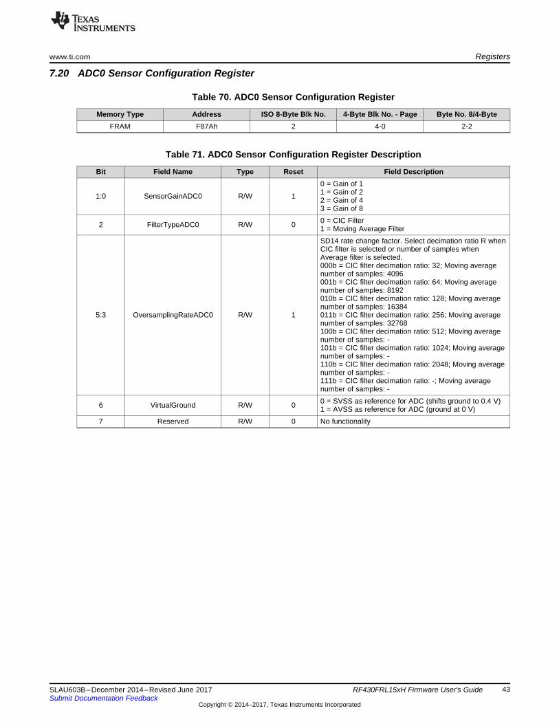
www.ti.com Registers
43SLAU603B–December 2014–Revised June 2017Submit Documentation Feedback
Copyright © 2014–2017, Texas Instruments Incorporated
RF430FRL15xH Firmware User's Guide
7.20 ADC0 Sensor Configuration Register
Table 70. ADC0 Sensor Configuration Register
Memory Type Address ISO 8-Byte Blk No. 4-Byte Blk No. - Page Byte No. 8/4-ByteFRAM F87Ah 2 4-0 2-2
Table 71. ADC0 Sensor Configuration Register Description
Bit Field Name Type Reset Field Description
1:0 SensorGainADC0 R/W 1
0 = Gain of 11 = Gain of 22 = Gain of 43 = Gain of 8
2 FilterTypeADC0 R/W 0 0 = CIC Filter1 = Moving Average Filter
5:3 OversamplingRateADC0 R/W 1
SD14 rate change factor. Select decimation ratio R whenCIC filter is selected or number of samples whenAverage filter is selected.000b = CIC filter decimation ratio: 32; Moving averagenumber of samples: 4096001b = CIC filter decimation ratio: 64; Moving averagenumber of samples: 8192010b = CIC filter decimation ratio: 128; Moving averagenumber of samples: 16384011b = CIC filter decimation ratio: 256; Moving averagenumber of samples: 32768100b = CIC filter decimation ratio: 512; Moving averagenumber of samples: -101b = CIC filter decimation ratio: 1024; Moving averagenumber of samples: -110b = CIC filter decimation ratio: 2048; Moving averagenumber of samples: -111b = CIC filter decimation ratio: -; Moving averagenumber of samples: -
6 VirtualGround R/W 0 0 = SVSS as reference for ADC (shifts ground to 0.4 V)1 = AVSS as reference for ADC (ground at 0 V)
7 Reserved R/W 0 No functionality

Registers www.ti.com
44 SLAU603B–December 2014–Revised June 2017Submit Documentation Feedback
Copyright © 2014–2017, Texas Instruments Incorporated
RF430FRL15xH Firmware User's Guide
7.21 Internal Sensor Configuration Register
Table 72. Internal Sensor Configuration Register
Memory Type Address ISO 8-Byte Blk No. 4-Byte Blk No. - Page Byte No. 8/4-ByteFRAM F87Bh 2 4-0 3-3
Table 73. ADC2 Sensor Configuration Register Description
Bit Field Name Type Reset Field Description
1:0 SensorGainInternal R/W 1
0 = Gain of 11 = Gain of 22 = Gain of 43 = Gain of 8
2 FilterTypeInternal R/W 0 0 = CIC Filter1 = Moving Average Filter
5:3 OversamplingRateInternal R/W 1
SD14 rate change factor. Select decimation ratio R whenCIC filter is selected or number of samples whenAverage filter is selected.000b = CIC filter decimation ratio: 32; Moving averagenumber of samples: 4096001b = CIC filter decimation ratio: 64; Moving averagenumber of samples: 8192010b = CIC filter decimation ratio: 128; Moving averagenumber of samples: 16384011b = CIC filter decimation ratio: 256; Moving averagenumber of samples: 32768100b = CIC filter decimation ratio: 512; Moving averagenumber of samples: -101b = CIC filter decimation ratio: 1024; Moving averagenumber of samples: -110b = CIC filter decimation ratio: 2048; Moving averagenumber of samples: -111b = CIC filter decimation ratio: -; Moving averagenumber of samples: -
6 VirtualGround R/W 0 0 = SVSS as reference for ADC (shifts ground to .4V)1 = AVSS as reference for ADC (ground at 0V)
7 Reserved R/W 0 No functionality
7.22 Initial Delay Period Setup Register
Table 74. Initial Delay Period Setup Register
Memory Type Address ISO 8-Byte Blk No. 4-Byte Blk No. - Page Byte No. 8/4-ByteFRAM F87Ch 2 5-0 4-0
Table 75. Initial Delay Period Setup Register Description
Bit Field Name Type Reset Field Description
7:0 InitialDelayPeriodSetup R/W 0Setting a nonzero value to this register enables the initialdelay of the value in minutes stored in the Initial DelayPeriod register.

www.ti.com Registers
45SLAU603B–December 2014–Revised June 2017Submit Documentation Feedback
Copyright © 2014–2017, Texas Instruments Incorporated
RF430FRL15xH Firmware User's Guide
7.23 JTAG Enable Password Register
Table 76. JTAG Enable Password Register
Memory Type Address ISO 8-Byte Blk No. 4-Byte Blk No. - Page Byte No. 8/4-ByteFRAM F87Dh 2 5-0 5-1
Table 77. JTAG Enable Password Register Description
Bit Field Name Type Reset Field Description
7:0 JTAGEnablePassword R/W UnchangedSetting this register to 0x39 will enable JTAG access. Beaware that the pins that JTAG replaces are set in anunknown state.
7.24 Initial Delay Period Register
Table 78. Initial Delay Period Register
Memory Type Address ISO 8-Byte Blk No. 4-Byte Blk No. - Page Byte No. 8/4-ByteFRAM F87Eh 2 5-0 6-2
Table 79. Initial Delay Period Register Description
Bit Field Name Type Reset Field Description
15:0 InitialDelayPeriod R/W Unchanged
This is the delay in minutes before sampling starts as configurednormally with the rest of the memory map. This feature onlybecomes activated when the Initial Delay Period Setup registeris set with a nonzero value.
7.25 Custom Timer Value Register
Table 80. Custom Timer Value Register
Memory Type Address ISO 8-Byte Blk No. 4-Byte Blk No. - Page Byte No. 8/4-ByteFRAM F880h 3 6-0 0-0
Table 81. Custom Timer Value Register Description
Bit Field Name Type Reset Field Description
31:0 CustomTime R/W Unchanged
The period time in milliseconds between consecutive scans.Same functionality as the Frequency register. The custom timeoption must be selected in the Frequency register for this time tobe used.
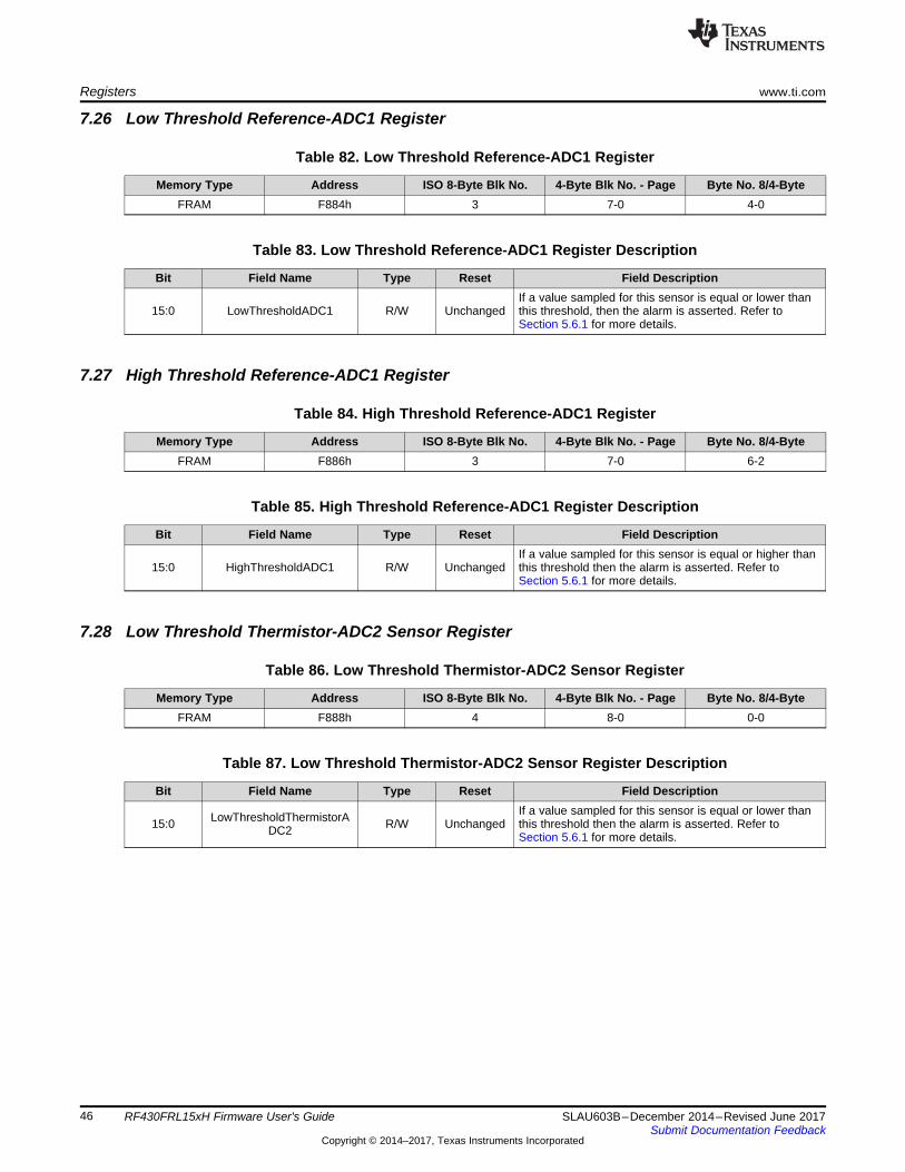
Registers www.ti.com
46 SLAU603B–December 2014–Revised June 2017Submit Documentation Feedback
Copyright © 2014–2017, Texas Instruments Incorporated
RF430FRL15xH Firmware User's Guide
7.26 Low Threshold Reference-ADC1 Register
Table 82. Low Threshold Reference-ADC1 Register
Memory Type Address ISO 8-Byte Blk No. 4-Byte Blk No. - Page Byte No. 8/4-ByteFRAM F884h 3 7-0 4-0
Table 83. Low Threshold Reference-ADC1 Register Description
Bit Field Name Type Reset Field Description
15:0 LowThresholdADC1 R/W UnchangedIf a value sampled for this sensor is equal or lower thanthis threshold, then the alarm is asserted. Refer toSection 5.6.1 for more details.
7.27 High Threshold Reference-ADC1 Register
Table 84. High Threshold Reference-ADC1 Register
Memory Type Address ISO 8-Byte Blk No. 4-Byte Blk No. - Page Byte No. 8/4-ByteFRAM F886h 3 7-0 6-2
Table 85. High Threshold Reference-ADC1 Register Description
Bit Field Name Type Reset Field Description
15:0 HighThresholdADC1 R/W UnchangedIf a value sampled for this sensor is equal or higher thanthis threshold then the alarm is asserted. Refer toSection 5.6.1 for more details.
7.28 Low Threshold Thermistor-ADC2 Sensor Register
Table 86. Low Threshold Thermistor-ADC2 Sensor Register
Memory Type Address ISO 8-Byte Blk No. 4-Byte Blk No. - Page Byte No. 8/4-ByteFRAM F888h 4 8-0 0-0
Table 87. Low Threshold Thermistor-ADC2 Sensor Register Description
Bit Field Name Type Reset Field Description
15:0 LowThresholdThermistorADC2 R/W Unchanged
If a value sampled for this sensor is equal or lower thanthis threshold then the alarm is asserted. Refer toSection 5.6.1 for more details.
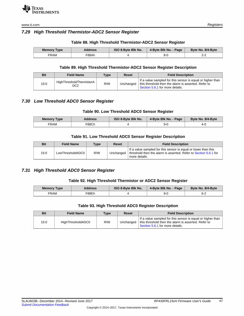
www.ti.com Registers
47SLAU603B–December 2014–Revised June 2017Submit Documentation Feedback
Copyright © 2014–2017, Texas Instruments Incorporated
RF430FRL15xH Firmware User's Guide
7.29 High Threshold Thermistor-ADC2 Sensor Register
Table 88. High Threshold Thermistor-ADC2 Sensor Register
Memory Type Address ISO 8-Byte Blk No. 4-Byte Blk No. - Page Byte No. 8/4-ByteFRAM F88Ah 4 8-0 2-2
Table 89. High Threshold Thermistor-ADC2 Sensor Register Description
Bit Field Name Type Reset Field Description
15:0 HighThresholdThermistorADC2 R/W Unchanged
If a value sampled for this sensor is equal or higher thanthis threshold then the alarm is asserted. Refer toSection 5.6.1 for more details.
7.30 Low Threshold ADC0 Sensor Register
Table 90. Low Threshold ADC0 Sensor Register
Memory Type Address ISO 8-Byte Blk No. 4-Byte Blk No. - Page Byte No. 8/4-ByteFRAM F88Ch 4 9-0 4-0
Table 91. Low Threshold ADC0 Sensor Register Description
Bit Field Name Type Reset Field Description
15:0 LowThresholdADC0 R/W UnchangedIf a value sampled for this sensor is equal or lower than thisthreshold then the alarm is asserted. Refer to Section 5.6.1 formore details.
7.31 High Threshold ADC0 Sensor Register
Table 92. High Threshold Thermistor or ADC2 Sensor Register
Memory Type Address ISO 8-Byte Blk No. 4-Byte Blk No. - Page Byte No. 8/4-ByteFRAM F88Eh 4 9-0 6-2
Table 93. High Threshold ADC0 Register Description
Bit Field Name Type Reset Field Description
15:0 HighThresholdADC0 R/W UnchangedIf a value sampled for this sensor is equal or higher thanthis threshold then the alarm is asserted. Refer toSection 5.6.1 for more details.
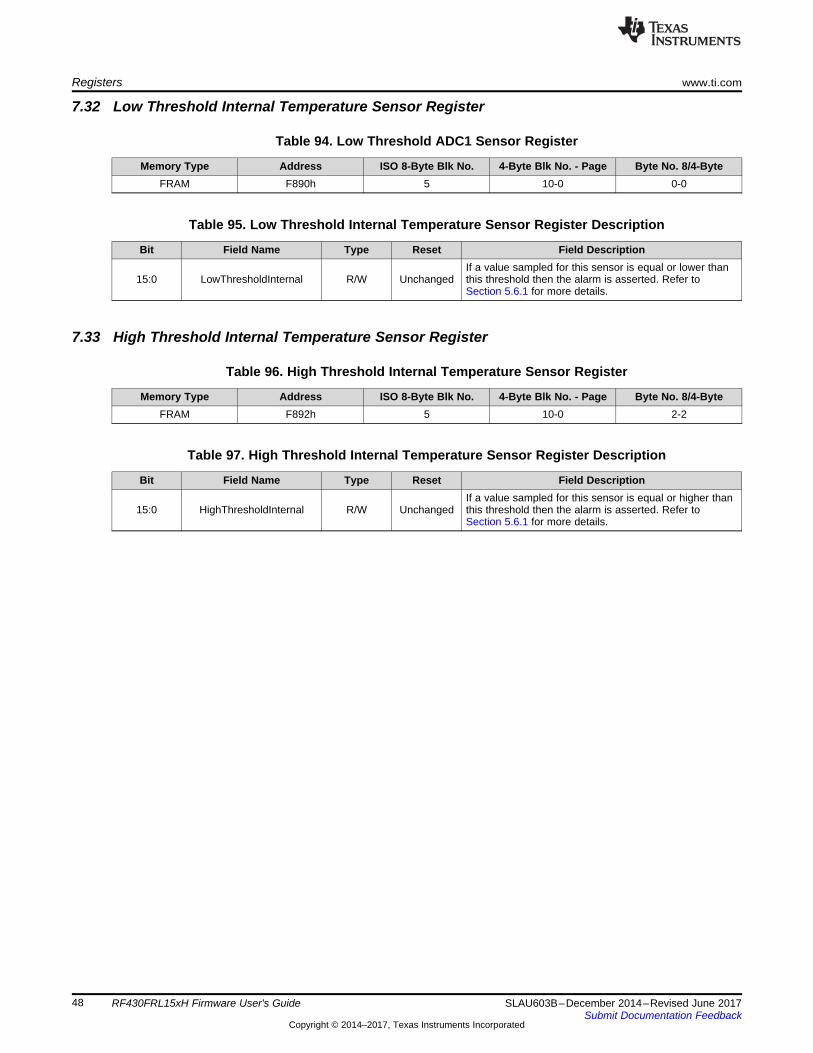
Registers www.ti.com
48 SLAU603B–December 2014–Revised June 2017Submit Documentation Feedback
Copyright © 2014–2017, Texas Instruments Incorporated
RF430FRL15xH Firmware User's Guide
7.32 Low Threshold Internal Temperature Sensor Register
Table 94. Low Threshold ADC1 Sensor Register
Memory Type Address ISO 8-Byte Blk No. 4-Byte Blk No. - Page Byte No. 8/4-ByteFRAM F890h 5 10-0 0-0
Table 95. Low Threshold Internal Temperature Sensor Register Description
Bit Field Name Type Reset Field Description
15:0 LowThresholdInternal R/W UnchangedIf a value sampled for this sensor is equal or lower thanthis threshold then the alarm is asserted. Refer toSection 5.6.1 for more details.
7.33 High Threshold Internal Temperature Sensor Register
Table 96. High Threshold Internal Temperature Sensor Register
Memory Type Address ISO 8-Byte Blk No. 4-Byte Blk No. - Page Byte No. 8/4-ByteFRAM F892h 5 10-0 2-2
Table 97. High Threshold Internal Temperature Sensor Register Description
Bit Field Name Type Reset Field Description
15:0 HighThresholdInternal R/W UnchangedIf a value sampled for this sensor is equal or higher thanthis threshold then the alarm is asserted. Refer toSection 5.6.1 for more details.

www.ti.com Registers
49SLAU603B–December 2014–Revised June 2017Submit Documentation Feedback
Copyright © 2014–2017, Texas Instruments Incorporated
RF430FRL15xH Firmware User's Guide
7.34 Low Threshold Digital1 Sensor Register
Table 98. Low Threshold Digital1 Sensor Register
Memory Type Address ISO 8-Byte Blk No. 4-Byte Blk No. - Page Byte No. 8/4-ByteFRAM F894h 5 11-0 4-0
Table 99. Low Threshold Digital1 Sensor Register Description
Bit Field Name Type Reset Field Description
15:0 LowThresholdDigital1 R/W UnchangedIf a value sampled for this sensor is equal or lower thanthis threshold then the alarm is asserted. Refer toSection 5.6.1 for more details.
7.35 High Threshold Digital1 Sensor Register
Table 100. High Threshold Digital1 Sensor Register
Memory Type Address ISO 8-Byte Blk No. 4-Byte Blk No. - Page Byte No. 8/4-ByteFRAM F896h 5 11-0 6-2
Table 101. High Threshold Digital1 Sensor Register Description
Bit Field Name Type Reset Field Description
15:0 HighThresholdDigital1 R/W UnchangedIf a value sampled for this sensor is equal or higher thanthis threshold then the alarm is asserted. Refer toSection 5.6.1 for more details.
7.36 Low Threshold Digital2 Sensor Register
Table 102. Low Threshold Digital2 Sensor Register
Memory Type Address ISO 8-Byte Blk No. 4-Byte Blk No. - Page Byte No. 8/4-ByteFRAM F898h 6 12-0 0-0
Table 103. Low Threshold Digital2 Sensor Register Description
Bit Field Name Type Reset Field Description
15:0 LowThresholdDigital2 R/W UnchangedIf a value sampled for this sensor is equal or lower thanthis threshold then the alarm is asserted. Refer toSection 5.6.1 for more details.
Registers www.ti.com
50 SLAU603B–December 2014–Revised June 2017Submit Documentation Feedback
Copyright © 2014–2017, Texas Instruments Incorporated
RF430FRL15xH Firmware User's Guide
7.37 High Threshold Digital2 Sensor Register
Table 104. High Threshold Digital2 Sensor Register
Memory Type Address ISO 8-Byte Blk No. 4-Byte Blk No. - Page Byte No. 8/4-ByteFRAM F89Ah 6 12-0 2-2
Table 105. High Threshold Digital2 Sensor Register Description
Bit Field Name Type Reset Field Description
15:0 HighThresholdDigital2 R/W UnchangedIf a value sampled for this sensor is equal or higher thanthis threshold then the alarm is asserted. Refer toSection 5.6.1 for more details.
7.38 Low Threshold Digital3 Sensor Register
Table 106. Low Threshold Digital3 Sensor Register
Memory Type Address ISO 8-Byte Blk No. 4-Byte Blk No. - Page Byte No. 8/4-ByteFRAM F89Ch 6 13-0 4-0
Table 107. Low Threshold Digital3 Sensor Register Description
Bit Field Name Type Reset Field Description
15:0 LowThresholdDigital1 R/W UnchangedIf a value sampled for this sensor is equal or lower thanthis threshold then the alarm is asserted. Refer toSection 5.6.1 for more details.
7.39 High Threshold Digital3 Sensor Register
Table 108. High Threshold Digital3 Sensor Register
Memory Type Address ISO 8-Byte Blk No. 4-Byte Blk No. - Page Byte No. 8/4-ByteFRAM F89Eh 6 13-0 6-2
Table 109. High Threshold Digital3 Sensor Register Description
Bit Field Name Type Reset Field Description
15:0 HighThresholdDigital3 R/W UnchangedIf a value sampled for this sensor is equal or higher thanthis threshold then the alarm is asserted. Refer toSection 5.6.1 for more details.

www.ti.com Registers
51SLAU603B–December 2014–Revised June 2017Submit Documentation Feedback
Copyright © 2014–2017, Texas Instruments Incorporated
RF430FRL15xH Firmware User's Guide
7.40 Reference or ADC1 Alarm Configuration Register
Table 110. Reference or ADC1 Alarm Configuration Register
Memory Type Address ISO 8-Byte Blk No. 4-Byte Blk No. - Page Byte No. 8/4-ByteFRAM F8A0h 7 14-0 0-0
Table 111. Reference or ADC1 Alarm Configuration Register Description
Bit Field Name Type Reset Field Description
1:0 PeakStoreADC1 R/W 0
0 = Store first value1 = Store highest value2 = lowest value3 = Average the group of valuesSetting used only if AveragingSamples is used
2 HighThresholdEnADC1 R/W 0 High threshold enable3 LowThresholdEnADC1 R/W 0 Low threshold enable4 LowThresholdAlrmADC1 R/W 0 Low threshold exceeded (monitor)5 HighThresholdAlrmADC1 R/W 0 High threshold exceeded (monitor)
6 InterruptADC1 R/W 0 Enables interrupt for this sensor if thresholds areexceeded (monitor must be set)
7 MonitorADC1 R/W 0 Enables alarm monitoring for this sensor (not theinterrupt)
7.41 Thermistor and ADC2 Alarm Configuration Register
Table 112. Thermistor and ADC2 Alarm Configuration Register
Memory Type Address ISO 8-Byte Blk No. 4-Byte Blk No. - Page Byte No. 8/4-ByteFRAM F8A1h 7 14-0 1-1
Table 113. Thermistor and ADC2 Alarm Configuration Description
Bit Field Name Type Reset Field Description
1:0 PeakStoreTherm R/W 0
0 = Store first value1 = Store highest value2 = Store lowest value3 = Average the group of valuesSetting used only if extra sampling is selected
2 HighThresholdEnTherm R/W 0 High threshold enable3 LowThresholdEnTherm R/W 0 Low threshold enable4 LowThresholdAlrmTherm R/W 0 Low threshold exceeded (monitor)5 HighThresholdAlrmTherm R/W 0 High threshold exceeded (monitor)
6 InterruptTherm R/W 0 Enables interrupt for this sensor if thresholds areexceeded (monitor must be set)
7 MonitorTherm R/W 0 Enables alarm monitoring for this sensor (not theinterrupt)
Registers www.ti.com
52 SLAU603B–December 2014–Revised June 2017Submit Documentation Feedback
Copyright © 2014–2017, Texas Instruments Incorporated
RF430FRL15xH Firmware User's Guide
7.42 ADC0 Alarm Configuration Register
Table 114. ADC0 Alarm Configuration Register
Memory Type Address ISO 8-Byte Blk No. 4-Byte Blk No. - Page Byte No. 8/4-ByteFRAM F8A2h 7 14-0 2-2
Table 115. ACD0 Alarm Configuration Register Description
Bit Field Name Type Reset Field Description
1:0 PeakStoreADC0 R/W 0
0 = Store first value1 = Store highest value2 = Store lowest value3 = Average the group of valuesSetting used only if extra sampling is selected
2 HighThresholdEnADC0 R/W 0 High threshold enable3 LowThresholdEnADC0 R/W 0 Low threshold enable4 LowThresholdAlrmADC0 R/W 0 Low threshold exceeded (monitor)5 HighThresholdAlrmADC0 R/W 0 High threshold exceeded (monitor)
6 InterruptADC0 R/W 0 Enables interrupt for this sensor if thresholds areexceeded (monitor must be set)
7 MonitorADC0 R/W 0 Enables alarm monitoring for this sensor (not theinterrupt)
7.43 Internal Alarm Configuration Register
Table 116. Internal Alarm Configuration Register
Memory Type Address ISO 8-Byte Blk No. 4-Byte Blk No. - Page Byte No. 8/4-ByteFRAM F8A3h 7 14-0 3-3
Table 117. Internal Alarm Configuration Register Description
Bit Field Name Type Reset Field Description
1:0 PeakStoreInter R/W 0
0 = Store first value1 = Store highest value2 = Store lowest value3 = Average the group of valuesSetting used only if extra sampling is selected
2 HighThresholdEnInter R/W 0 High threshold enable3 LowThresholdEnInter R/W 0 Low threshold enable4 LowThresholdAlrmInter R/W 0 Low threshold exceeded (monitor)5 HighThresholdAlrmInter R/W 0 High threshold exceeded (monitor)
6 InterruptInternal R/W 0 Enables interrupt for this sensor if thresholds areexceeded (monitor must be set)
7 MonitorInter R/W 0 Enables alarm monitoring for this sensor (not theinterrupt)
www.ti.com Registers
53SLAU603B–December 2014–Revised June 2017Submit Documentation Feedback
Copyright © 2014–2017, Texas Instruments Incorporated
RF430FRL15xH Firmware User's Guide
7.44 Digital 1 Alarm Configuration Register
Table 118. Digital 1 Alarm Configuration Register
Memory Type Address ISO 8-Byte Blk No. 4-Byte Blk No. - Page Byte No. 8/4-ByteFRAM F8A4h 7 15-0 4-0
Table 119. Digital 1 Alarm Configuration Register Description
Bit Field Name Type Reset Field Description
1:0 PeakStoreDigital2 R/W 0
0 = Store first value1 = Store highest value2 = Store lowest value3 = Average the group of valuesSetting used only if extra sampling is selected
2 HighThresholdDigital2 R/W 0 High threshold enable3 LowThresholdDigital2 R/W 0 Low threshold enable4 LowThresholdAlrmDigital2 R/W 0 Low threshold exceeded (monitor)5 HighThresholdAlrmDigital2 R/W 0 High threshold exceeded (monitor)
6 InterruptDigital2 R/W 0 Enables interrupt for this sensor if thresholds areexceeded (monitor must be set)
7 MonitorDigital2 R/W 0 Enables alarm monitoring for this sensor (not theinterrupt)
7.45 Digital 2 Alarm Configuration Register
Table 120. Digital 2 Alarm Configuration Register
Memory Type Address ISO 8-Byte Blk No. 4-Byte Blk No. - Page Byte No. 8/4-ByteFRAM F8A5h 7 15-0 5-1
Table 121. Digital 2 Alarm Configuration Register Description
Bit Field Name Type Reset Field Description
1:0 PeakStoreDigital2 R/W 0
0 = Store first value1 = Store highest value2 = Store lowest value3 = Average the group of valuesSetting used only if extra sampling is selected
2 HighThresholdDigital2 R/W 0 High threshold enable3 LowThresholdDigital2 R/W 0 Low threshold enable4 LowThresholdAlrmDigital2 R/W 0 Low threshold exceeded (monitor)5 HighThresholdAlrmDigital2 R/W 0 High threshold exceeded (monitor)
6 InterruptDigital2 R/W 0 Enables interrupt for this sensor if thresholds areexceeded (monitor must be set)
7 MonitorDigital2 R/W 0 Enables alarm monitoring for this sensor (not theinterrupt)
Registers www.ti.com
54 SLAU603B–December 2014–Revised June 2017Submit Documentation Feedback
Copyright © 2014–2017, Texas Instruments Incorporated
RF430FRL15xH Firmware User's Guide
7.46 Digital 3 Alarm Configuration Register
Table 122. Digital 3 Alarm Configuration Register
Memory Type Address ISO 8-Byte Blk No. 4-Byte Blk No. - Page Byte No. 8/4-ByteFRAM F8A6h 7 15-0 6-2
Table 123. Digital 3 Alarm Configuration Register Description
Bit Field Name Type Reset Field Description
1:0 PeakStoreDigita3 R/W 0
0 = Store first value1 = Store highest value2 = Store lowest value3 = Average the group of valuesSetting used only if extra sampling is selected
2 HighThresholdDigital3 R/W 0 High threshold enable3 LowThresholdDigital3 R/W 0 Low threshold enable4 LowThresholdAlrmDigital3 R/W 0 Low threshold exceeded (monitor)5 HighThresholdAlrmDigital3 R/W 0 High threshold exceeded (monitor)
6 InterruptDigital3 R/W 0 Enables interrupt for this sensor if thresholds areexceeded (monitor must be set)
7 MonitorDigital3 R/W 0 Enables alarm monitoring for this sensor (not theinterrupt)
7.47 Logging Memory Size Register
Table 124. Logging Memory Size Register
Memory Type Address ISO 8-Byte Blk No. 4-Byte Blk No. - Page Byte No. 8/4-ByteFRAM F8A8h 8 16-0 0-0
Table 125. Logging Memory Size Register Description
Bit Field Name Type Reset Field Description
15:0 MemorySize R/W 504
Automatically populated to 504 on power up with uninitializedFRAM memory or on software reset. Changeable to any value.Although if this setting is too high, during execution and storageof data corruption of patch functions may occur(which mayfollow the samples stored) or the interrupt vectors likely disablingthe chip and requiring reprogramming.Refer to the memory map layout for determining the maximumvalue.

www.ti.com Registers
55SLAU603B–December 2014–Revised June 2017Submit Documentation Feedback
Copyright © 2014–2017, Texas Instruments Incorporated
RF430FRL15xH Firmware User's Guide
7.48 Total Number of Stores Register
Table 126. Total Number of Stores Register
Memory Type Address ISO 8-Byte Blk No. 4-Byte Blk No. - Page Byte No. 8/4-ByteFRAM F8AA 8 16-0 2-2
Table 127. Total Number of Stores Register Description
Bit Field Name Type Reset Field Description
15:0 NumberOfStores R/W 0
The number of stores that have occurred during the samplingprocess.This register is only really necessary to determine where in thesampling process the device was when the infinite sampling wasstopped.The reset of 0 is only done on the start of the sampling process.
7.49 Last Logged Index Register
Table 128. Sampling Buffer Index Register
Memory Type Address ISO 8-Byte Blk No. 4-Byte Blk No. - Page Byte No. 8/4-ByteFRAM F8AC 8 17-0 4-0
Table 129. Sampling Buffer Index Register Description
Bit Field Name Type Reset Field Description
15:0 BufferIndex R/W 0
The index location of the last data stored from the samplingprocess. For example, 200 means that 200 values were writtento the data buffer (RAM or FRAM).The reset of 0 is only done on the start of the sampling process.
7.50 FRAM Data Valid Register
Table 130. FRAM Data Valid Register
Memory Type Address ISO 8-Byte Blk No. 4-Byte Blk No. - Page Byte No. 8/4-ByteFRAM F8AE 8 17-0 6-2
Table 131. FRAM Data Valid Register Description
Bit Field Name Type Reset Field Description
15:0 FRAMDataValid R/W 0xA3A6
This is used by internally by the firmware to detect if FRAM mustbe initialized.If this register is not set to 0xA3A6, then after reset the firmwarewill initialize the FRAM memory map to default values.

Registers www.ti.com
56 SLAU603B–December 2014–Revised June 2017Submit Documentation Feedback
Copyright © 2014–2017, Texas Instruments Incorporated
RF430FRL15xH Firmware User's Guide
7.51 Logging Memory Space
Table 132. Logging FRAM Memory Space
Memory Type Address ISO 8-Byte Blk No. 4-Byte Block Range Length (Max)
FRAM Starts at F8B0h 9-236 18-242(pg0),0-230(pg1) 1824 bytes
Table 133. Logging FRAM Memory Space Description
Bit Field Name Type Reset Field Description
– SamplesLocation R/W 504
This is the location where the data is stored after sampling thesensors. It is in integer format (16 bits long).This is the default size; it may be increased by changing theLogging Memory Size Register field, which would extend thebuffer.This is not an actual register, just a memory space.There is a choice between using FRAM or RAM as data storage.This is done in RAMStorage of the control-status block.This variable is only initialized on reset when the FRAM DataValid register is not set to the correct value.
Table 134. Logging Location Register
Memory Type Address ISO 8-Byte BlockRange
4-Byte Block Range Length (Max)
RAM 1E00h to 2BFFh 600h to 800h 600h to 1000h 3583 bytes
Table 135. Logging Location Register Description
Bit Field Name Type Reset Field Description
– SamplesLocation – –
This is the location where the data is stored after sampling thesensors. It is in integer format (16 bits long).This is the defaultsize; it may be increased by changing the Logging Memory SizeRegister field, which would extend the buffer.This is not an actual register, just a memory space
7.52 Firmware Version RegisterThe device firmware version may be read by issue a read single block command to block 0xFB. Theapplication version response is in the first byte. The rest of the bytes will fill with zeros for the block sizeused.
Table 136. Firmware Version Register
Memory Type Address ISO 8-Byte Blk No. 4-Byte Blk No. - Page Byte No. 8/4-ByteROM 5FFEh FBh FBh FBh
Table 137. Firmware Version Register Description
Bit Field Name Type Reset Field Description3:0 MinorFirmwareVersion R 0 The minor version of the firmware version.7:4 MajorFirmwareVersion R 1 The major version of the firmware version.
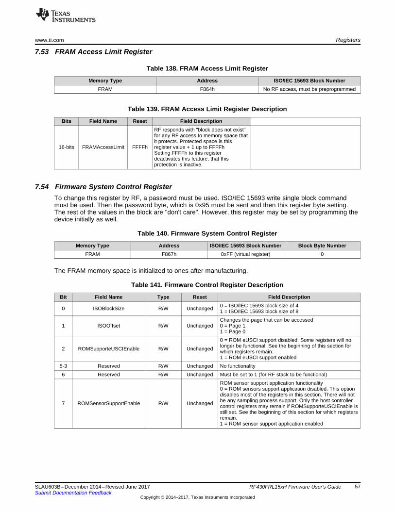
www.ti.com Registers
57SLAU603B–December 2014–Revised June 2017Submit Documentation Feedback
Copyright © 2014–2017, Texas Instruments Incorporated
RF430FRL15xH Firmware User's Guide
7.53 FRAM Access Limit Register
Table 138. FRAM Access Limit Register
Memory Type Address ISO/IEC 15693 Block NumberFRAM F864h No RF access, must be preprogrammed
Table 139. FRAM Access Limit Register Description
Bits Field Name Reset Field Description
16-bits FRAMAccessLimit FFFFh
RF responds with "block does not exist"for any RF access to memory space thatit protects. Protected space is thisregister value + 1 up to FFFFhSetting FFFFh to this registerdeactivates this feature, that thisprotection is inactive.
7.54 Firmware System Control RegisterTo change this register by RF, a password must be used. ISO/IEC 15693 write single block commandmust be used. Then the password byte, which is 0x95 must be sent and then this register byte setting.The rest of the values in the block are "don't care". However, this register may be set by programming thedevice initially as well.
Table 140. Firmware System Control Register
Memory Type Address ISO/IEC 15693 Block Number Block Byte NumberFRAM F867h 0xFF (virtual register) 0
The FRAM memory space is initialized to ones after manufacturing.
Table 141. Firmware Control Register Description
Bit Field Name Type Reset Field Description
0 ISOBlockSize R/W Unchanged 0 = ISO/IEC 15693 block size of 41 = ISO/IEC 15693 block size of 8
1 ISOOffset R/W UnchangedChanges the page that can be accessed0 = Page 11 = Page 0
2 ROMSupporteUSCIEnable R/W Unchanged
0 = ROM eUSCI support disabled. Some registers will nolonger be functional. See the beginning of this section forwhich registers remain.1 = ROM eUSCI support enabled
5-3 Reserved R/W Unchanged No functionality6 Reserved R/W Unchanged Must be set to 1 (for RF stack to be functional)
7 ROMSensorSupportEnable R/W Unchanged
ROM sensor support application functionality0 = ROM sensors support application disabled. This optiondisables most of the registers in this section. There will notbe any sampling process support. Only the host controllercontrol registers may remain if ROMSupporteUSCIEnable isstill set. See the beginning of this section for which registersremain.1 = ROM sensor support application enabled

Production Programming www.ti.com
58 SLAU603B–December 2014–Revised June 2017Submit Documentation Feedback
Copyright © 2014–2017, Texas Instruments Incorporated
RF430FRL15xH Firmware User's Guide
8 Production ProgrammingThis device has some unique behavior when used with programmers.
Due to the behavior described below, these devices fail a blank check after FRAM memory erase. This isbecause the ROM firmware initializes various parts of the FRAM memory after reset based on theconditions in Table 142.
Table 142. ROM Firmware Initialization
Initialization Part NumbersAffected After Reset Condition Result
1RF430FRL152HRF430FRL153HRF430FRL154H
Address: 0xFFFE(Reset vector)
= 0xFFFF
0xF864 to 0xF8AF0xFFD8 to 0xFFFFAre updated by the ROM(not necessarily each byte)
Any other value No changes to 0xFFD8 to 0xFFFF section
2 RF430FRL152HRF430FRL153H
Address: 0xF8AE(FRAM Data Valid register)
= 0xA3A6 No changes
Any other valueInitialization of FRAM area by ROM code:0xF868 to 0xF8AE(not necessarily each byte)
If the ROM firmware functionality is not used, then initialization 2 is not present. Initialization 1 is possiblein all cases if the condition is met. The initialization order is as numbered.
9 Adding Custom CommandsThe RF430FRL15xH devices can add ISO/IEC custom commands to the RF stack. The commands areadded through a table that is parsed on reset (see Table 143).
The ISO/IEC 15693 custom commands must be defined in the table before the ROM commands. Whenthe parser reaches a ROM patch ID, any ISO/IEC 15693 commands that are listed later in the table arenot recognized.
Table 143. Patching Table Format
Address Value Description0xFFCE 0xCECE The table (also called "driver") start key. If not present, then no updating is performed.
0xFFCC Command ID
If Command ID has only the low byte defined (for example, 0x00xx), then this representsan ISO/IEC 15693 command. For example, a Patch ID of 0x00AA adds a 0xAA customcommand.If Command ID has only the high byte defined (for example, 0xNN00), then this representsa ROM function to be patched. This functionality is described for informational purposesonly; the user is not expected to make changes to the ROM functionality.
0xFFCA Function Address These two bytes describe the address of the function that it is defined in. This can be inRAM or FRAM.
0xFFC8 Command ID The command ID and function address can continue in pairs as needed.0xFFC6 Function Address The command ID and function address can continue in pairs as needed.0xFFC4 0xCECE Table ending key.
9.1 Custom Command FormatTable 144 describes the custom ISO/IEC 15693 command format.
Table 144. Custom Command Format Table
Flags Command Manufacturer ID Optional Data
0x02(for high speed) 0xA0 to 0xDF 0x07 (TI)
Read register RF13MTXF_L for 8 bits from RF FIFO or readRF13MTXF for 16 bits of data (read repeatedly for more data).The custom command must follow the response timing requirements ofthe ISO/IEC 15693 specification.
www.ti.com Revision History
59SLAU603B–December 2014–Revised June 2017Submit Documentation Feedback
Copyright © 2014–2017, Texas Instruments Incorporated
Revision History
Revision HistoryNOTE: Page numbers for previous revisions may differ from page numbers in the current version.
Changes from July 23, 2016 to June 28, 2017 ................................................................................................................. Page
• Removed NFC Bridge row in Table 1, Operational Modes .......................................................................... 4• Removed former Section 1.5, NFC Bridge............................................................................................. 4• Added Equation 3 in Section 2.8.2, Thermistor Resistance Calculation ......................................................... 10• Removed former Section 4.15, NFC Bridge.......................................................................................... 19• Corrected the SPI signal names on P1.0 and P1.1 in Table 21, General-Purpose Port Definitions.......................... 19• Removed reference to NFC Bridge in Table 31, Memory Reserved in RF Stack Only Project ............................... 28• Removed reference to NFC Bridge in Table 35, General Control Register Description ....................................... 33• Corrected the value in the Length column in Table 134, Logging Location Register........................................... 56• Removed reference to NFC Bridge in Table 141, Firmware Control Register Description .................................... 57
IMPORTANT NOTICE FOR TI DESIGN INFORMATION AND RESOURCES
Texas Instruments Incorporated (‘TI”) technical, application or other design advice, services or information, including, but not limited to,reference designs and materials relating to evaluation modules, (collectively, “TI Resources”) are intended to assist designers who aredeveloping applications that incorporate TI products; by downloading, accessing or using any particular TI Resource in any way, you(individually or, if you are acting on behalf of a company, your company) agree to use it solely for this purpose and subject to the terms ofthis Notice.TI’s provision of TI Resources does not expand or otherwise alter TI’s applicable published warranties or warranty disclaimers for TIproducts, and no additional obligations or liabilities arise from TI providing such TI Resources. TI reserves the right to make corrections,enhancements, improvements and other changes to its TI Resources.You understand and agree that you remain responsible for using your independent analysis, evaluation and judgment in designing yourapplications and that you have full and exclusive responsibility to assure the safety of your applications and compliance of your applications(and of all TI products used in or for your applications) with all applicable regulations, laws and other applicable requirements. Yourepresent that, with respect to your applications, you have all the necessary expertise to create and implement safeguards that (1)anticipate dangerous consequences of failures, (2) monitor failures and their consequences, and (3) lessen the likelihood of failures thatmight cause harm and take appropriate actions. You agree that prior to using or distributing any applications that include TI products, youwill thoroughly test such applications and the functionality of such TI products as used in such applications. TI has not conducted anytesting other than that specifically described in the published documentation for a particular TI Resource.You are authorized to use, copy and modify any individual TI Resource only in connection with the development of applications that includethe TI product(s) identified in such TI Resource. NO OTHER LICENSE, EXPRESS OR IMPLIED, BY ESTOPPEL OR OTHERWISE TOANY OTHER TI INTELLECTUAL PROPERTY RIGHT, AND NO LICENSE TO ANY TECHNOLOGY OR INTELLECTUAL PROPERTYRIGHT OF TI OR ANY THIRD PARTY IS GRANTED HEREIN, including but not limited to any patent right, copyright, mask work right, orother intellectual property right relating to any combination, machine, or process in which TI products or services are used. Informationregarding or referencing third-party products or services does not constitute a license to use such products or services, or a warranty orendorsement thereof. Use of TI Resources may require a license from a third party under the patents or other intellectual property of thethird party, or a license from TI under the patents or other intellectual property of TI.TI RESOURCES ARE PROVIDED “AS IS” AND WITH ALL FAULTS. TI DISCLAIMS ALL OTHER WARRANTIES ORREPRESENTATIONS, EXPRESS OR IMPLIED, REGARDING TI RESOURCES OR USE THEREOF, INCLUDING BUT NOT LIMITED TOACCURACY OR COMPLETENESS, TITLE, ANY EPIDEMIC FAILURE WARRANTY AND ANY IMPLIED WARRANTIES OFMERCHANTABILITY, FITNESS FOR A PARTICULAR PURPOSE, AND NON-INFRINGEMENT OF ANY THIRD PARTY INTELLECTUALPROPERTY RIGHTS.TI SHALL NOT BE LIABLE FOR AND SHALL NOT DEFEND OR INDEMNIFY YOU AGAINST ANY CLAIM, INCLUDING BUT NOTLIMITED TO ANY INFRINGEMENT CLAIM THAT RELATES TO OR IS BASED ON ANY COMBINATION OF PRODUCTS EVEN IFDESCRIBED IN TI RESOURCES OR OTHERWISE. IN NO EVENT SHALL TI BE LIABLE FOR ANY ACTUAL, DIRECT, SPECIAL,COLLATERAL, INDIRECT, PUNITIVE, INCIDENTAL, CONSEQUENTIAL OR EXEMPLARY DAMAGES IN CONNECTION WITH ORARISING OUT OF TI RESOURCES OR USE THEREOF, AND REGARDLESS OF WHETHER TI HAS BEEN ADVISED OF THEPOSSIBILITY OF SUCH DAMAGES.You agree to fully indemnify TI and its representatives against any damages, costs, losses, and/or liabilities arising out of your non-compliance with the terms and provisions of this Notice.This Notice applies to TI Resources. Additional terms apply to the use and purchase of certain types of materials, TI products and services.These include; without limitation, TI’s standard terms for semiconductor products http://www.ti.com/sc/docs/stdterms.htm), evaluationmodules, and samples (http://www.ti.com/sc/docs/sampterms.htm).
Mailing Address: Texas Instruments, Post Office Box 655303, Dallas, Texas 75265Copyright © 2017, Texas Instruments Incorporated


![NXP JCOP Java Card Product Range - cardlogix.com · NXP NFC IC’s Product Features PN512 PN532 PN533 PN544 Operating distance up to [mm] (1) 70 70 70 70 ... 13.56 13.56 13.56 13.56](https://img.pdfslide.net/doc/110x75/5b9cc5d209d3f2df1f8b81a9/nxp-jcop-java-card-product-range-nxp-nfc-ics-product-features-pn512-pn532.jpg)