Embed Size (px)
Citation preview

WHITE PAPER
RF/Microwave Technology Driving the Connected Car
In-car networks and advanced driver-assistance systems (ADAS), made possible through
wireless sensors, driver-assist radar, vehicle communications, and related electronics, present
many design challenges to engineers. Simulation software enables design teams to effectively
manage the complex design and integration challenges associated with developing these
high-speed and RF-enabled networks. Through proper analysis and design automation
software from Cadence, engineering teams can accelerate the design of robust devices to
meet performance, size, weight, and cost requirements while reducing time to market.
This white paper looks at Cadence® AWR Design Environment® software solutions for RF to
millimeter-wave (mmWave) front-end component development through the Cadence
Intelligent System Design™ portfolio to specifically address electronic product development
for automotive applications.
Contents
Design Overview ...............................................................................2
Challenges for ADAS Design and Analysis ...............................2
Radar Design ......................................................................................5
60GHz FMCW MIMO Radar Example ............................................8
77GHz Antenna Array Design ......................................................10
EM Analysis for Design Verification ........................................... 13
AiP Solutions ....................................................................................14
Conclusion ........................................................................................ 16
References ....................................................................................... 16
RF/Microwave Technology Driving the Connected Car
2www.cadence.com/go/awr
Design OverviewThe Society of Automotive Engineers (SAE) has defined five levels of driver assist/autonomous driving capabilities that will gradually transition the driving experience from largely human controlled to fully automated (Figure 1).
Figure 1: SAE autonomous driving levels
These levels are driven by factors that include consumer adoption (influenced by demographics such as age, income, location, etc.), economics/costs, and technology, especially performance. While select companies have demonstrated some initial vehicles operating at Level 4 in the robotaxi and luxury car markets, most automakers’ fleets operate between Levels 2 and 3 of autonomy.
Challenges for ADAS Design and AnalysisDriver assist systems are composed of many different functions requiring a wide range of environmental monitoring, analysis, feedback, and controls or driver alerts. Current environmental monitoring is performed by different sensor types such as cameras and lidar and radar technologies, each used for different applications depending on strength and economical advantage. Advances in RF front-end, antenna, and packaging technologies combine with artificial intelligence (AI) and vehicle-to-everything (V2X) communications to play a critical role in enabling higher levels of autonomous driving.
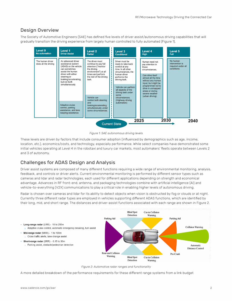
Radar is chosen over cameras and lidar for its ability to detect objects when vision is obstructed by fog or clouds or at night. Currently three different radar types are employed in vehicles supporting different ADAS functions, which are identified by their long, mid, and short range. The distances and driver-assist functions associated with each range are shown in Figure 2.
Figure 2: Automotive radar ranges and functionality
A more detailed breakdown of the performance requirements for these different range systems from a link budget
RF/Microwave Technology Driving the Connected Car
3www.cadence.com/go/awr
perspective is shown in Table 1. Today’s ADAS systems call for larger available bandwidth to provide better resolution. 77GHz automotive radar applications use the frequency range from 76-81GHz with a bandwidth of over 4GHz as compared to a bandwidth of 200MHz available for automotive radar applications at 24GHz. This wider bandwidth increases the range and velocity resolution of the radar, allowing it to identify objects that are closely spaced.
Table 1: Automotive radar performance requirements for SAE Level 2 (Source: J. Hasch et. Al., IEEE Trans. Micr. Theory Tech, 2012)
Radars need to be able to determine differences in phase between transmitted and received signals to measure the relative velocity of an object. As the wavelength decreases, the resolution and accuracy of this velocity measurement improves proportionally. Therefore, as sensors move from 24GHz to 77GHz, velocity measurements can improve by 3X.
Another advantage at 77GHz is the decrease in antenna size, which is proportional to wavelength. 77GHz radars have higher permitted transmit power levels, where the effective isotropic radiated power (EIRP) is 55dBm (-3dBm/MHz). For 24GHz radars, the peak limit is only 20dBm EIRP. While 77GHz has many benefits, the designer faces challenges such as more propa-gation and circuit loss. Cadence AWR® Visual System Simulator™ (VSS) system design software provides link budget analysis for determining the optimum system configuration from a high-level system perspective and helps system architects to determine their transmitter/receiver (TX/RX) line-up requirements, partitioning, and individual component specifications.
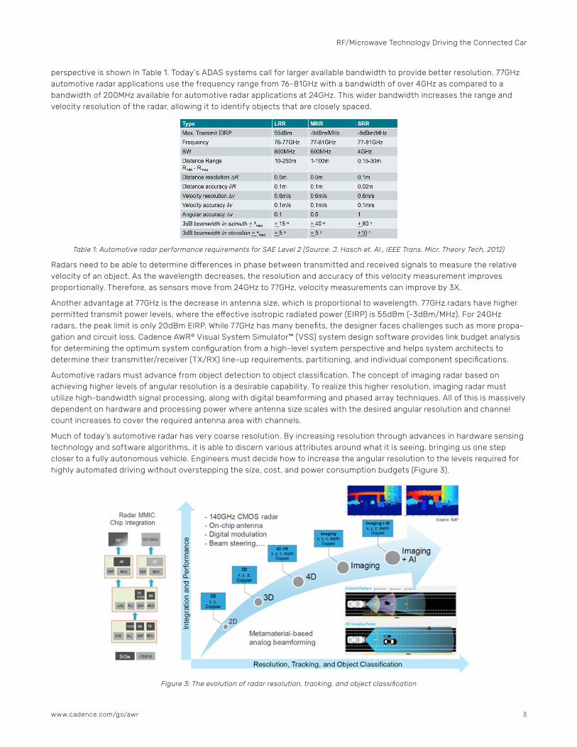
Automotive radars must advance from object detection to object classification. The concept of imaging radar based on achieving higher levels of angular resolution is a desirable capability. To realize this higher resolution, imaging radar must utilize high-bandwidth signal processing, along with digital beamforming and phased array techniques. All of this is massively dependent on hardware and processing power where antenna size scales with the desired angular resolution and channel count increases to cover the required antenna area with channels.
Much of today’s automotive radar has very coarse resolution. By increasing resolution through advances in hardware sensing technology and software algorithms, it is able to discern various attributes around what it is seeing, bringing us one step closer to a fully autonomous vehicle. Engineers must decide how to increase the angular resolution to the levels required for highly automated driving without overstepping the size, cost, and power consumption budgets (Figure 3).
Figure 3: The evolution of radar resolution, tracking, and object classification
RF/Microwave Technology Driving the Connected Car
4www.cadence.com/go/awr
In addition, designers need to increase the number of reflection points from low reflectivity targets while dramatically reducing the latency of detection to improve response time and allowing vehicles to take evasive action in an emergency. Furthermore, they must optimize the form factor (size, weight, and power) while maintaining a high level of performance that also considers cost or economic factors. Chip, package, and board co-design are critical to achieving these goals, and, recog-nizing these challenges, Cadence has embarked on its Intelligent System Design strategy to help customers achieve cross-fabric design and system integration success.
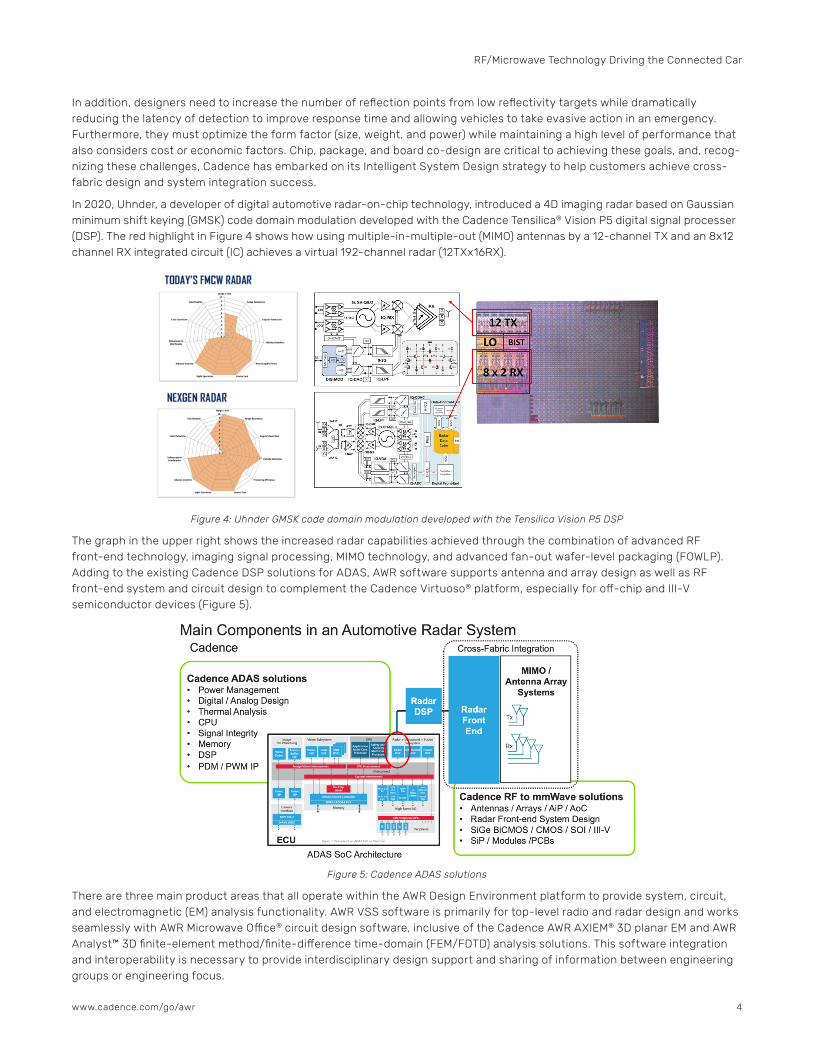
In 2020, Uhnder, a developer of digital automotive radar-on-chip technology, introduced a 4D imaging radar based on Gaussian minimum shift keying (GMSK) code domain modulation developed with the Cadence Tensilica® Vision P5 digital signal processer (DSP). The red highlight in Figure 4 shows how using multiple-in-multiple-out (MIMO) antennas by a 12-channel TX and an 8x12 channel RX integrated circuit (IC) achieves a virtual 192-channel radar (12TXx16RX).
Figure 4: Uhnder GMSK code domain modulation developed with the Tensilica Vision P5 DSP
The graph in the upper right shows the increased radar capabilities achieved through the combination of advanced RF front-end technology, imaging signal processing, MIMO technology, and advanced fan-out wafer-level packaging (FOWLP). Adding to the existing Cadence DSP solutions for ADAS, AWR software supports antenna and array design as well as RF front-end system and circuit design to complement the Cadence Virtuoso® platform, especially for off-chip and III-V semiconductor devices (Figure 5).
Figure 5: Cadence ADAS solutions
There are three main product areas that all operate within the AWR Design Environment platform to provide system, circuit, and electromagnetic (EM) analysis functionality. AWR VSS software is primarily for top-level radio and radar design and works seamlessly with AWR Microwave Office® circuit design software, inclusive of the Cadence AWR AXIEM® 3D planar EM and AWR Analyst™ 3D finite-element method/finite-difference time-domain (FEM/FDTD) analysis solutions. This software integration and interoperability is necessary to provide interdisciplinary design support and sharing of information between engineering groups or engineering focus.
RF/Microwave Technology Driving the Connected Car
5www.cadence.com/go/awr
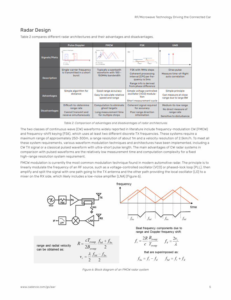
Radar DesignTable 2 compares different radar architectures and their advantages and disadvantages.
Table 2: Comparison of advantages and disadvantages of radar architectures
The two classes of continuous wave (CW) waveforms widely reported in literature include frequency-modulation CW (FMCW) and frequency-shift keying (FSK), which uses at least two different discrete TX frequencies. These systems require a maximum range of approximately 250-300m, a range resolution of about 1m and a velocity resolution of 2.5km/h. To meet all these system requirements, various waveform modulation techniques and architectures have been implemented, including a CW TX signal or a classical pulsed waveform with ultra-short pulse length. The main advantages of CW radar systems in comparison with pulsed waveforms are the relatively low measurement time and computation complexity for a fixed high-range resolution system requirement.
FMCW modulation is currently the most common modulation technique found in modern automotive radar. The principle is to linearly modulate the frequency of an RF source, such as a voltage-controlled oscillator (VCO) or phased-lock loop (PLL), then amplify and split the signal with one path going to the TX antenna and the other path providing the local oscillator (LO) to a mixer on the RX side, which likely includes a low-noise amplifier (LNA) (Figure 6).
Figure 6: Block diagram of an FMCW radar system
RF/Microwave Technology Driving the Connected Car
6www.cadence.com/go/awr
Since the signal’s frequency is continually shifting as a function of time, the frequency of the received signal that has been reflected off a target will be different than the LO signal. The mixer product or intermediate frequency (IF) signal will be the difference in these frequencies, and because the rate of the frequency modulation is known, the time delay can be deter-mined, which enables the designer to determine the range or distance of the target. Through Doppler shifting, the relative speed of the object in relationship to the radar can also be determined.
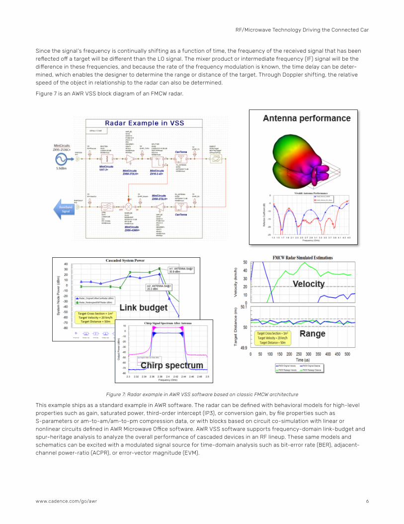
Figure 7 is an AWR VSS block diagram of an FMCW radar.
Figure 7: Radar example in AWR VSS software based on classic FMCW architecture
This example ships as a standard example in AWR software. The radar can be defined with behavioral models for high-level properties such as gain, saturated power, third-order intercept (IP3), or conversion gain, by file properties such as S-parameters or am-to-am/am-to-pm compression data, or with blocks based on circuit co-simulation with linear or nonlinear circuits defined in AWR Microwave Office software. AWR VSS software supports frequency-domain link-budget and spur-heritage analysis to analyze the overall performance of cascaded devices in an RF lineup. These same models and schematics can be excited with a modulated signal source for time-domain analysis such as bit-error rate (BER), adjacent-channel power-ratio (ACPR), or error-vector magnitude (EVM).
RF/Microwave Technology Driving the Connected Car
7www.cadence.com/go/awr
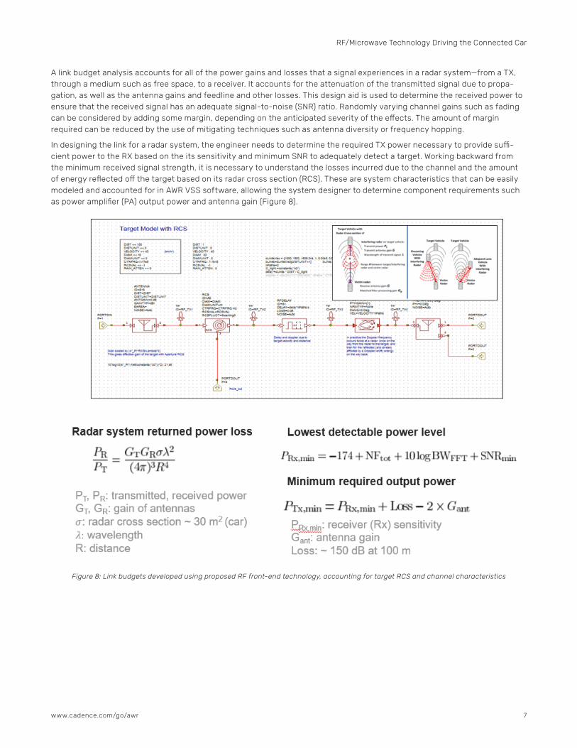
A link budget analysis accounts for all of the power gains and losses that a signal experiences in a radar system—from a TX, through a medium such as free space, to a receiver. It accounts for the attenuation of the transmitted signal due to propa-gation, as well as the antenna gains and feedline and other losses. This design aid is used to determine the received power to ensure that the received signal has an adequate signal-to-noise (SNR) ratio. Randomly varying channel gains such as fading can be considered by adding some margin, depending on the anticipated severity of the effects. The amount of margin required can be reduced by the use of mitigating techniques such as antenna diversity or frequency hopping.
In designing the link for a radar system, the engineer needs to determine the required TX power necessary to provide suffi-cient power to the RX based on the its sensitivity and minimum SNR to adequately detect a target. Working backward from the minimum received signal strength, it is necessary to understand the losses incurred due to the channel and the amount of energy reflected off the target based on its radar cross section (RCS). These are system characteristics that can be easily modeled and accounted for in AWR VSS software, allowing the system designer to determine component requirements such as power amplifier (PA) output power and antenna gain (Figure 8).
Figure 8: Link budgets developed using proposed RF front-end technology, accounting for target RCS and channel characteristics
RF/Microwave Technology Driving the Connected Car
8www.cadence.com/go/awr
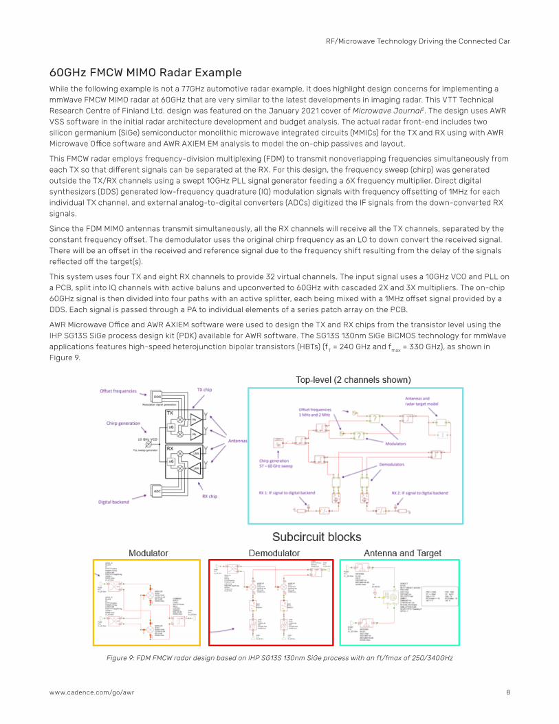
60GHz FMCW MIMO Radar ExampleWhile the following example is not a 77GHz automotive radar example, it does highlight design concerns for implementing a mmWave FMCW MIMO radar at 60GHz that are very similar to the latest developments in imaging radar. This VTT Technical Research Centre of Finland Ltd. design was featured on the January 2021 cover of Microwave Journal2. The design uses AWR VSS software in the initial radar architecture development and budget analysis. The actual radar front-end includes two silicon germanium (SiGe) semiconductor monolithic microwave integrated circuits (MMICs) for the TX and RX using with AWR Microwave Office software and AWR AXIEM EM analysis to model the on-chip passives and layout.
This FMCW radar employs frequency-division multiplexing (FDM) to transmit nonoverlapping frequencies simultaneously from each TX so that different signals can be separated at the RX. For this design, the frequency sweep (chirp) was generated outside the TX/RX channels using a swept 10GHz PLL signal generator feeding a 6X frequency multiplier. Direct digital synthesizers (DDS) generated low-frequency quadrature (IQ) modulation signals with frequency offsetting of 1MHz for each individual TX channel, and external analog-to-digital converters (ADCs) digitized the IF signals from the down-converted RX signals.
Since the FDM MIMO antennas transmit simultaneously, all the RX channels will receive all the TX channels, separated by the constant frequency offset. The demodulator uses the original chirp frequency as an LO to down convert the received signal. There will be an offset in the received and reference signal due to the frequency shift resulting from the delay of the signals reflected off the target(s).
This system uses four TX and eight RX channels to provide 32 virtual channels. The input signal uses a 10GHz VCO and PLL on a PCB, split into IQ channels with active baluns and upconverted to 60GHz with cascaded 2X and 3X multipliers. The on-chip 60GHz signal is then divided into four paths with an active splitter, each being mixed with a 1MHz offset signal provided by a DDS. Each signal is passed through a PA to individual elements of a series patch array on the PCB.
AWR Microwave Office and AWR AXIEM software were used to design the TX and RX chips from the transistor level using the IHP SG13S SiGe process design kit (PDK) available for AWR software. The SG13S 130nm SiGe BiCMOS technology for mmWave applications features high-speed heterojunction bipolar transistors (HBTs) (fT = 240 GHz and fmax = 330 GHz), as shown in Figure 9.
Figure 9: FDM FMCW radar design based on IHP SG13S 130nm SiGe process with an ft/fmax of 250/340GHz
RF/Microwave Technology Driving the Connected Car
9www.cadence.com/go/awr
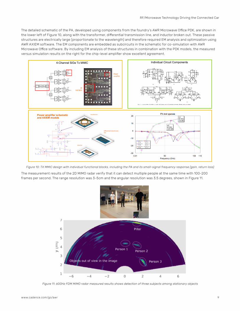
The detailed schematic of the PA, developed using components from the foundry’s AWR Microwave Office PDK, are shown in the lower left of Figure 10, along with the transformer, differential transmission line, and inductor broken out. These passive structures are electrically large (proportionate to the wavelength) and therefore required EM analysis and optimization using AWR AXIEM software. The EM components are embedded as subcircuits in the schematic for co-simulation with AWR Microwave Office software. By including EM analysis of these structures in combination with the PDK models, the measured versus simulation results on the right for the chip-level amplifier show excellent agreement.
Figure 10: TX MMIC design with individual functional blocks, including the PA and its small-signal frequency response (gain, return loss)
The measurement results of the 2D MIMO radar verify that it can detect multiple people at the same time with 100-200 frames per second. The range resolution was 3-5cm and the angular resolution was 3.5 degrees, shown in Figure 11.
Figure 11: 60GHz FDM MIMO radar measured results shows detection of three subjects among stationary objects
RF/Microwave Technology Driving the Connected Car
10www.cadence.com/go/awr
77GHz Antenna Array DesignThe future of automotive radar will require a significant improvement to image definitions derived from radar signals. This can be made possible through adoption of MIMO and beam steering phased array antennas. AWR VSS and AWR AXIEM software can be combined to provide a powerful phased array design solution, supporting antenna modeling via EM analysis and rapid phased array configuration for physical realization, as well as link budgeting and initial system architecture and design with AWR VSS software.
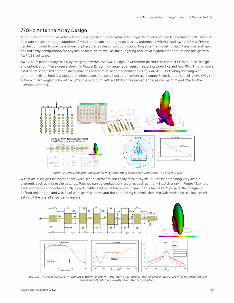
AWR AXIEM planar analysis is fully integrated within the AWR Design Environment platform to support EM/circuit co-design and optimization. The example shown in Figure 12 is a mid-range radar sensor featuring three TXs and four RXs. This mmWave fixed beam series-fed antenna array provides optimum in-band performance using AWR AXIEM EM analysis along with parametrically defined (variable patch dimensions and spacings) patch antennas. It supports horizontal field-of-views (FOV) of 160m with ±6° angle, 100m with a ±9° angle, and 60m with a ±10° for the main antenna, as well as 36m and 12m for the elevation antenna.
Figure 12: Series-fed antenna array for mid-range radar sensor featuring three TXs and four RXs
Within AWR Design Environment software, planar elements can easily form array structures by combining very simple elements such as microstrip patches. Patches can be configured in a series such as the 1x8 patch array in Figure 13, where each element is connected serially by a “tunable” section of transmission line. In this AWR AXIEM project, the designers defined the lengths and widths of each array element and the connecting transmission lines with variables to allow optimi-zation of the overall array performance.
Figure 13: The AWR Design Environment platform, along with the AWR AXIEM and/or AWR Analyst analysis, allow for optimization of a series-fed x8 patch array with parameterized modifiers
RF/Microwave Technology Driving the Connected Car
11www.cadence.com/go/awr
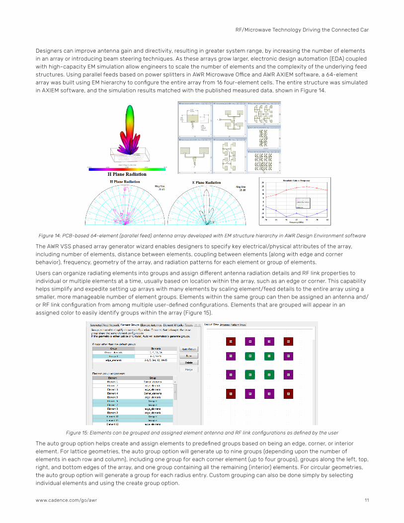
Designers can improve antenna gain and directivity, resulting in greater system range, by increasing the number of elements in an array or introducing beam steering techniques. As these arrays grow larger, electronic design automation (EDA) coupled with high-capacity EM simulation allow engineers to scale the number of elements and the complexity of the underlying feed structures. Using parallel feeds based on power splitters in AWR Microwave Office and AWR AXIEM software, a 64-element array was built using EM hierarchy to configure the entire array from 16 four-element cells. The entire structure was simulated in AXIEM software, and the simulation results matched with the published measured data, shown in Figure 14.
Figure 14: PCB-based 64-element (parallel feed) antenna array developed with EM structure hierarchy in AWR Design Environment software
The AWR VSS phased array generator wizard enables designers to specify key electrical/physical attributes of the array, including number of elements, distance between elements, coupling between elements (along with edge and corner behavior), frequency, geometry of the array, and radiation patterns for each element or group of elements.
Users can organize radiating elements into groups and assign different antenna radiation details and RF link properties to individual or multiple elements at a time, usually based on location within the array, such as an edge or corner. This capability helps simplify and expedite setting up arrays with many elements by scaling element/feed details to the entire array using a smaller, more manageable number of element groups. Elements within the same group can then be assigned an antenna and/or RF link configuration from among multiple user-defined configurations. Elements that are grouped will appear in an assigned color to easily identify groups within the array (Figure 15).
Figure 15: Elements can be grouped and assigned element antenna and RF link configurations as defined by the user
The auto group option helps create and assign elements to predefined groups based on being an edge, corner, or interior element. For lattice geometries, the auto group option will generate up to nine groups (depending upon the number of elements in each row and column), including one group for each corner element (up to four groups), groups along the left, top, right, and bottom edges of the array, and one group containing all the remaining (interior) elements. For circular geometries, the auto group option will generate a group for each radius entry. Custom grouping can also be done simply by selecting individual elements and using the create group option.
RF/Microwave Technology Driving the Connected Car
12www.cadence.com/go/awr
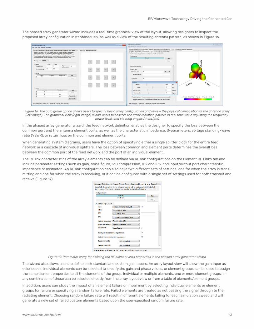
The phased array generator wizard includes a real-time graphical view of the layout, allowing designers to inspect the proposed array configuration instantaneously, as well as a view of the resulting antenna pattern, as shown in Figure 16.
Figure 16: The auto group option allows users to specify basic array configuration and review the physical composition of the antenna array (left image). The graphical view (right image) allows users to observe the array radiation pattern in real time while adjusting the frequency,
power level, and steering angles (theta/phi)
In the phased array generator wizard, the feed network definition enables the designer to specify the loss between the common port and the antenna element ports, as well as the characteristic impedance, S-parameters, voltage standing-wave ratio (VSWR), or return loss on the common and element ports.
When generating system diagrams, users have the option of specifying either a single splitter block for the entire feed network or a cascade of individual splitters. The loss between common and element ports determines the overall loss between the common port of the feed network and the port of an individual element.
The RF link characteristics of the array elements can be defined via RF link configurations on the Element RF Links tab and include parameter settings such as gain, noise figure, 1dB compression, IP2 and IP3, and input/output port characteristic impedance or mismatch. An RF link configuration can also have two different sets of settings, one for when the array is trans-mitting and one for when the array is receiving, or it can be configured with a single set of settings used for both transmit and receive (Figure 17).
Figure 17: Parameter entry for defining the RF element links properties in the phased array generator wizard
The wizard also allows users to define both standard and custom gain tapers. An array layout view will show the gain taper as color coded. Individual elements can be selected to specify the gain and phase values, or element groups can be used to assign the same element properties to all the elements of the group. Individual or multiple elements, one or more element groups, or any combination of these can be selected directly from the array layout view or from a table of elements/element groups.
In addition, users can study the impact of an element failure or impairment by selecting individual elements or element groups for failure or specifying a random failure rate. Failed elements are treated as not passing the signal through to the radiating element. Choosing random failure rate will result in different elements failing for each simulation sweep and will generate a new set of failed custom elements based upon the user-specified random failure rate.
RF/Microwave Technology Driving the Connected Car
13www.cadence.com/go/awr
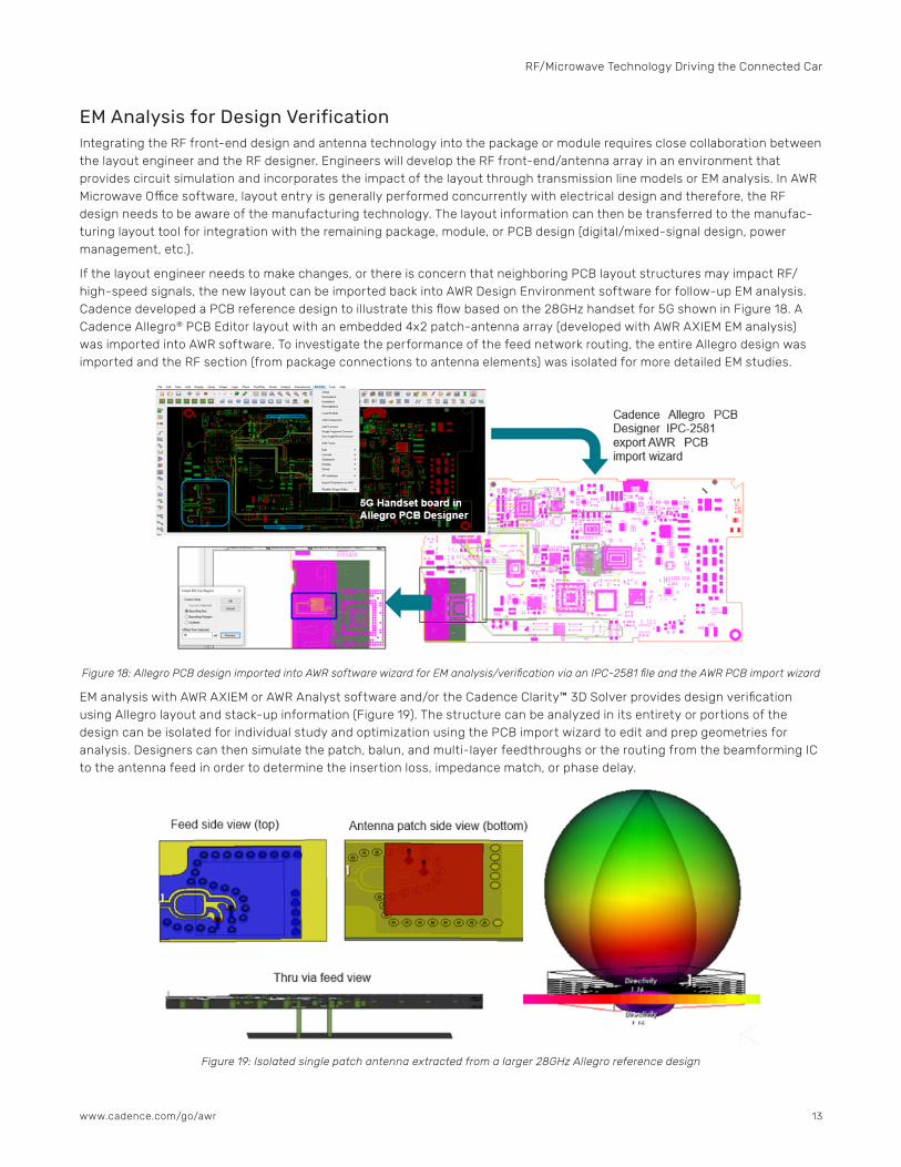
EM Analysis for Design VerificationIntegrating the RF front-end design and antenna technology into the package or module requires close collaboration between the layout engineer and the RF designer. Engineers will develop the RF front-end/antenna array in an environment that provides circuit simulation and incorporates the impact of the layout through transmission line models or EM analysis. In AWR Microwave Office software, layout entry is generally performed concurrently with electrical design and therefore, the RF design needs to be aware of the manufacturing technology. The layout information can then be transferred to the manufac-turing layout tool for integration with the remaining package, module, or PCB design (digital/mixed-signal design, power management, etc.).
If the layout engineer needs to make changes, or there is concern that neighboring PCB layout structures may impact RF/high-speed signals, the new layout can be imported back into AWR Design Environment software for follow-up EM analysis. Cadence developed a PCB reference design to illustrate this flow based on the 28GHz handset for 5G shown in Figure 18. A Cadence Allegro® PCB Editor layout with an embedded 4x2 patch-antenna array (developed with AWR AXIEM EM analysis) was imported into AWR software. To investigate the performance of the feed network routing, the entire Allegro design was imported and the RF section (from package connections to antenna elements) was isolated for more detailed EM studies.
Figure 18: Allegro PCB design imported into AWR software wizard for EM analysis/verification via an IPC-2581 file and the AWR PCB import wizard
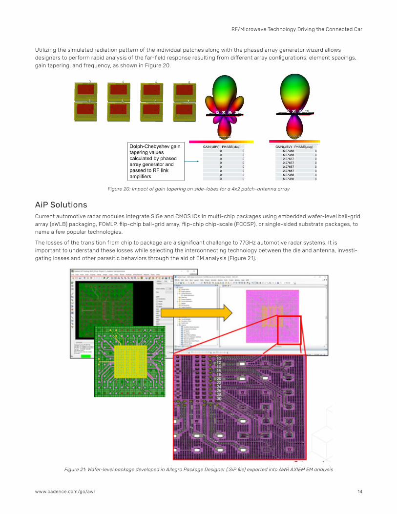
EM analysis with AWR AXIEM or AWR Analyst software and/or the Cadence Clarity™ 3D Solver provides design verification using Allegro layout and stack-up information (Figure 19). The structure can be analyzed in its entirety or portions of the design can be isolated for individual study and optimization using the PCB import wizard to edit and prep geometries for analysis. Designers can then simulate the patch, balun, and multi-layer feedthroughs or the routing from the beamforming IC to the antenna feed in order to determine the insertion loss, impedance match, or phase delay.
Figure 19: Isolated single patch antenna extracted from a larger 28GHz Allegro reference design
RF/Microwave Technology Driving the Connected Car
14www.cadence.com/go/awr
Utilizing the simulated radiation pattern of the individual patches along with the phased array generator wizard allows designers to perform rapid analysis of the far-field response resulting from different array configurations, element spacings, gain tapering, and frequency, as shown in Figure 20.
Figure 20: Impact of gain tapering on side-lobes for a 4x2 patch-antenna array
AiP SolutionsCurrent automotive radar modules integrate SiGe and CMOS ICs in multi-chip packages using embedded wafer-level ball-grid array (eWLB) packaging, FOWLP, flip-chip ball-grid array, flip-chip chip-scale (FCCSP), or single-sided substrate packages, to name a few popular technologies.
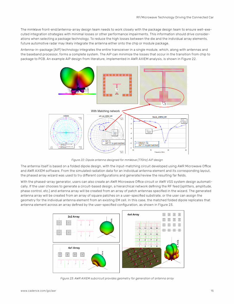
The losses of the transition from chip to package are a significant challenge to 77GHz automotive radar systems. It is important to understand these losses while selecting the interconnecting technology between the die and antenna, investi-gating losses and other parasitic behaviors through the aid of EM analysis (Figure 21).
Figure 21: Wafer-level package developed in Allegro Package Designer (.SiP file) exported into AWR AXIEM EM analysis
RF/Microwave Technology Driving the Connected Car
15www.cadence.com/go/awr
The mmWave front-end/antenna-array design team needs to work closely with the package design team to ensure well-exe-cuted integration strategies with minimal losses or other performance impairments. This information should drive consider-ations when selecting a package technology. To reduce the high losses between the die and the individual array elements, future automotive radar may likely integrate the antenna either onto the chip or module package.
Antenna-in-package (AiP) technology integrates the entire transceiver in a single module, which, along with antennas and the baseband processor, forms a complete system. The AiP can minimize the losses that occur in the transition from chip to package to PCB. An example AiP design from literature, implemented in AWR AXIEM analysis, is shown in Figure 22.
Figure 22: Dipole antenna designed for mmWave (77GHz) AiP design
The antenna itself is based on a folded dipole design, with the input-matching circuit developed using AWR Microwave Office and AWR AXIEM software. From the simulated radiation data for an individual antenna element and its corresponding layout, the phased array wizard was used to try different configurations and generate/review the resulting far fields.
With the phased-array generator, users can also create an AWR Microwave Office circuit or AWR VSS system design automati-cally. If the user chooses to generate a circuit-based design, a hierarchical network defining the RF feed (splitters, amplitude, phase control, etc.) and antenna array will be created from an array of patch antennas specified in the wizard. The generated antenna array will be created from an array of square patches on a user-specified substrate, or the user can assign the geometry for the individual antenna element from an existing EM cell. In this case, the matched folded dipole replicates that antenna element across an array defined by the user-specified configuration, as shown in Figure 23.
Figure 23: AWR AXIEM subcircuit provides geometry for generation of antenna array

RF/Microwave Technology Driving the Connected Car
Cadence is a pivotal leader in electronic design and computational expertise, using its Intelligent System Design strategy to turn design concepts into reality. Cadence customers are the world’s most creative and innovative companies, delivering extraordinary electronic products from chips to boards to systems for the most dynamic market applications. www.cadence.com
© 2021 Cadence Design Systems, Inc. All rights reserved worldwide. Cadence, the Cadence logo, and the other Cadence marks found at www.cadence.com/go/trademarks are trademarks or registered trademarks of Cadence Design Systems, Inc. All other trademarks are the property of their respective owners. 15911 03/21 DB/SA/WP-CNCT-CAR/PDF
ConclusionFor tomorrow’s ADAS-enabled vehicles, 4D imaging radar is needed for object recognition, which is the gateway to the next levels of autonomous driving. System analysis plays a key role in linking radar sensing (RF front-end) requirements to current and future signal processing capabilities to make imaging radar possible. In addition, MIMO and phased-array antennas will provide improved RF signal propagation, leading to true 4D imaging radars for SAE Levels 4 and higher ADAS. Modules based on advanced packaging technology are needed to integrate image signal processing, power management, SiGe BiCMOS/CMOS RF front-ends, and in-package or on-chip antenna arrays into a high-performance system for automotive guidance and driver assist radars.