Embed Size (px)
Citation preview

RHD2000 USB/FPGA Interface: Rhythm
www.intantech.com ● [email protected] 1
intan TECHNOLOGIES, LLC
RHD2000
USB/FPGA Interface: Rhythm
Version 1.5, 3 May 2016
Features ♦ Open-source Verilog hardware description language
(HDL) code configures a Xilinx field-programmable gate array (FPGA) to communicate with multiple RHD2000 digital electrophysiology interface chips
♦ Verilog code is written for a commercially-available Opal Kelly XEM6010 module with integrated high-speed USB 2.0 interface
♦ Up to 256 simultaneous amplifier channels supported at sample rates up to 30 kS/s/channel
♦ Programmable FPGA clock for RHD2000 interface: sample rates from 1 kS/s/channel to 30 kS/s/channel supported
♦ Open-source host computer application programming interface (API) in C++ for multi-platform support
♦ Module can interface with eight 16-bit digital-to-analog converters (DACs) and route selected amplifier channels to selected DACs for analog signal reconstruction or audio monitoring with minimal latency
♦ Optional control of eight 16-bit analog-to-digital converters (ADCs) for auxiliary analog inputs synchronized to all RHD2000 amplifier channels
♦ Auxiliary digital I/O: 16 digital input lines and 16 digital output lines supported
Applications ♦ Windows, Mac, or Linux-based electrophysiology signal
acquisition systems ♦ Rapid prototyping of Intan Technologies RHD2000-
based products ♦ Starting point for the development of custom interfaces
to RHD2000 chips
Description To facilitate the development of electrophysiology recording systems using the new RHD2000 series of microchips, Intan Technologies provides the following open-source USB/FPGA interface for developers. Designated Rhythm, the interface consists of Verilog HDL code written for the commercially-available Opal Kelly XEM6010 USB/FPGA interface module and a C++ API. Rhythm configures the Xilinx FPGA on the Opal Kelly module to communicate with up to eight RHD2000 chips over LVDS SPI buses and to stream data from these chips to a host computer over a high-speed USB 2.0 interface.
The Opal Kelly drivers and Rhythm software interfaces are designed for multi-platform development under Windows, Mac, or Linux. All API software is written in C++ to facilitate rapid development. This datasheet provides documentation on the Rhythm hardware and software protocols so that developers may quickly link the RHD2000 chips to a host computer of their choice.
Rhythm supports real-time streaming of up to 256 amplifier channels from multiple RHD2000 chips, auxiliary data from the chips (e.g., special chip functions such as temperature sensing), data from up to eight other ADCs, and signals from 16 digital inputs. All data is synchronized and time-stamped before transmission over a standard USB 2.0 bus to the host computer.
The host computer may configure the Rhythm-based module to set the RHD2000 per-channel sampling rate between 1 kS/s and 30 kS/s for a wide variety of electrophysiology recording applications (e.g., neural spikes, EMG, EKG). Custom RHD2000 command sequences may be uploaded to the FPGA for transmission over the SPI buses. Selected amplifier channels may be directly routed to eight optional DACs for analog signal reconstruction or audio monitoring with minimal latency.
intan TECHNOLOGIES, LLC

RHD2000 USB/FPGA Interface: Rhythm
www.intantech.com ● [email protected] 2
intan TECHNOLOGIES, LLC
Rhythm FPGA I/O Signals General Description The Rhythm interface code is designed for the Opal Kelly XEM6010-LX45 USB/FPGA module which is a small commercially-available circuit board containing a Xilinx Spartan-6 FPGA (XC6SLX45-2), a 128-MByte SDRAM chip, a 100-MHz clock source, I/O connectors, and a USB 2.0 interface chip capable of streaming data to a host computer at rates exceeding 20 MByte/s. (A photo of the board is shown on page 1 of this datasheet. See http://www.opalkelly.com for detailed information on this module.) A similar Opal Kelly module, the XEM6110v2-LX45, offers the same hardware with a PCI Express interface for significantly higher data rates and lower latencies (at the expense of a more complicated bus architecture). The Opal Kelly XEM6310 board offers similar hardware with a USB 3.0 interface capable of significantly higher data rates with latencies similar to USB 2.0.
The Spartan-6 FPGA is a digital chip containing hundreds of thousands of configurable logic gates, flip-flops, and memory cells with programmable connections between them. The FPGA is configured by means of a bitfile, which is compiled from Verilog HDL (Hardware Description Language) code using the free Xilinx ISE WebPack software (available from http://www.xilinx.com). The bitfile must be uploaded to the FPGA through the host computer interface (USB or PCI Express) every time the board is powered up; it is not stored in non-volatile RAM on the FPGA or the Opal Kelly module. Since this “booting” process takes only a fraction of a second, the flexibility it imparts becomes a useful feature: any changes made to the bitfile can be incorporated into a software release. The FPGA never needs to be programmed using a special EEPROM programmer or JTAG interface.
The Rhythm Verilog code from Intan Technologies uses less than half of the logic resources on the XC6SLC45-2 FPGA, leaving significant amounts of logic gates and on-FPGA memory for developers to add functionality (e.g., real-time signal processing and feedback for closed-loop control). Opal Kelly also offers the XEM6010-LX150 USB/FPGA module which is identical to the XEM6010-LX45 except for the use of an XC6SLX150-2 FPGA which contains approximately three times as many logic gates as the XC6SLX45-2. Developers who wish to add significant amounts of processing at the FPGA level may wish to use this module. However, to compile Verilog HDL into bitfiles for this larger FPGA, developers must use Xilinx’s ISE Logic Edition software instead of the free WebPack. Also, the XEM6110 PCI Express interface board is only available with the smaller LX45 FPGA.
The diagram below shows the main elements on the Opal Kelly XEM6010 board and the I/O signals defined by Rhythm.

RHD2000 USB/FPGA Interface: Rhythm
www.intantech.com ● [email protected] 3
intan TECHNOLOGIES, LLC
RHD2000 SPI Interfaces Rhythm sets up four SPI ports (labeled A, B, C, and D) that can send independent command streams to different sets of RHD2000 chips over LVDS wire pairs. (Each arrow on the right side of the previous diagram represents an LVDS signal pair.) If non-LVDS communication is required, it is easy to change the Verilog code to configure the FPGA to communicate using standard 3.3V CMOS signals on a subset of these I/O pins. However, LVDS communication is recommended for low-noise operation and data reliability on long cables. (See the RHD2000 datasheet for more details.)
Each SPI port on the FPGA has three output signals that coordinate communication with RHD2000 chips and send commands: CS, SCLK, and MOSI (Master Out, Slave In). The FPGA always acts as the SPI master device, and each RHD2000 acts as an SPI slave device. Each SPI port in Rhythm has two MISO (Master In, Slave Out) inputs for receiving data from an RHD2000 chip. This means that each port can be connected to two RHD2000 chips, but both of these chips will receive the same commands. So, for example, the auxiliary digital output pin on the two RHD2000 chips cannot be set to different values. For most applications this is not a serious restriction, and it permits the construction of compact 128-channel recording modules using two RHD2164 chips, for example. Each module requires a 12-conductor cable to support five LVDS SPI signals plus power and ground.
The use of LVDS signals permits robust data transfer over cables several meters in length. However, long cables will introduce significant delays to the SPI signals. Typical cable propagation velocities are two-thirds the speed of light – about 20 cm/ns – so a three-meter cable will have a round-trip signal delay of 30 ns. (At high sampling rates, the SCLK period may be less than 50 ns.) Rhythm allows users to adjust the MISO sampling delay independently on all four SPI ports to account for cable delays.
Using dual MISO signals on each of four ports, the FPGA can stream data from up to eight RHD2000 chips. If RHD2132 chips or four RHD2164 chip are used, a total of 256 amplifier channels may be acquired in real time. The USB 2.0 interface on the Opal Kelly XEM6010 module is capable of reliably streaming data from 256 channels to a host computer at per-channel sampling rates up to 30 kS/s, even with typical USB protocol overhead and software overhead. (The XEM6310 USB 3.0 module and the XEM6110 PCI Express module are capable of much higher data transfer rates, but these have not been tested at Intan Technologies.)
Rhythm sends commands to all RHD2000 chips in a repeating 35-command sequence: every sampling period, the FPGA sends the commands CONVERT(0), CONVERT(1), CONVERT(2), and so on up to CONVERT(31) to sample from all 32 amplifiers on the chip. (If the 16-channel RHD2216 chip is used, the last 16 CONVERT commands produce junk results that can be ignored.) These 32 CONVERT commands are followed by three “auxiliary” commands that may be used to perform a variety of other tasks on an RHD2000 chip, like synthesizing a waveform for electrode impedance testing, reading from the auxiliary inputs or temperature sensor, performing ADC calibration, or reading and writing other registers. Under Rhythm, the first 32 CONVERT commands are fixed, but the remaining auxiliary commands may be programmed from the host computer.
A clock generator on the Opal Kelly circuit board provides a 100-MHz clock to the FPGA; this clock is used to run the USB interface logic. Rhythm controls an on-FPGA frequency synthesizer that is used to generate a programmable-frequency clock that can be reconfigured by the host computer to produce many different SPI data rates so that the RHD2000 amplifiers can be sampled at per-channel rates varying from 1 kS/s to 30 kS/s.
Other I/O Signals Rhythm also defines I/O pins that can be connected to several commercially-available 16-bit DACs and ADCs. The Verilog code supports up to eight 16-bit DACs and eight 16-bit ADCs that communicate using a three-wire SPI interface. Rhythm is designed to support the Analog Devices AD5662 DAC and the Analog Devices AD7680 ADC; other DACs and ADCs could be supported by modifying the Verilog code. Rhythm permits the user to select particular RHD2000 amplifier channels to be routed directly to selected DACs through the FPGA, eliminating any USB or host computer latency. Alternatively, any of the DACs may be controlled by a dedicated data stream from the host computer if more latency can be tolerated.
The optional ADCs are sampled in synchrony with the RHD2000 amplifiers, and their results are streamed back to the host computer over the USB interface.
Rhythm also supports 16 digital inputs and 16 digital outputs. The digital outputs produce 3.3V signals. The digital inputs have a logic threshold around 1.5V and can safely accept signals up to 5V.
Eight of the digital outputs may serve as low-latency threshold comparators for the signals routed to the DACs. Threshold levels and polarities may be specified, and the FPGA will trigger the appropriate digital outputs if each threshold is exceeded.

RHD2000 USB/FPGA Interface: Rhythm
www.intantech.com ● [email protected] 4
intan TECHNOLOGIES, LLC
The Opal Kelly board has an array of eight red LEDs (in addition to a green power LED) that may be controlled by the host computer.
A digital output signal sample_clk is provided on FPGA pin L51P as a convenience. This signal is a clock running at the per-channel amplifier sampling rate. The duty cycle of the signal is 1/35. For example, if the board is configured to sample each RHD2000 amplifier channel at 20 kS/s than the period of this clock will be 50 µs. It will be high for approximately 1.43 µs, and low the rest of the cycle. (The signal goes high at the falling edge of CS that begins the CONVERT(0) command, and it goes low at the falling edge of CS that begins the CONVERT(1) command.)
Power Supply The total current consumption of the XEM6010 board running Rhythm is approximately 470 mA from 5V, not including current consumed by RHD2000 chips and other ADCs and DACs. Current supplied from a USB port is limited to 500 mA. Since a Rhythm-based module will likely exceed this limit once RHD2000 chips and other ADCs and DACs are added, it is recommended to power the Opal Kelly XEM6010 board from a 5V DC power supply capable of sourcing sufficient current and having a 2.1mm inner-diameter / 5.5mm outer-diameter connector. Opal Kelly offers a PSS050-25 power supply that provides up to 2.5 A of current. Digi-Key (http://www.digikey.com) offers a medical-rated power supply that mates with the XEM6010 board, supplies up to 2.0 A of current, and includes connectors for AC plugs in a variety of countries (part number T1233-P5P-ND).
The Opal Kelly board provides regulated 1.2V, 1.8V, and 3.3V supplies. See the Opal Kelly documentation for current limits on these supplies.
If RHD2000 chips will be powered over long cables, it is a good idea use a linear regulator to generate a 3.5V power supply from the 5V power delivered to the board. RHD2000 chips may be safely powered at 3.5V, and the excess 0.2 V above the nominal power supply voltage of 3.3V will make up for some of the IR losses incurred over long cables with thin power wires.
I/O Pin Locations The I/O pin tables on the following two pages are based on pages 22 and 23 of the Opal Kelly XEM6010 User’s Manual.
Note: If the XEM6110 PCI Express board is used, the I/O signals are the same, but “JP2” from the XEM6010 board has been renamed to JP1, and “JP3” from the XEM6010 board has been renamed to JP2. (See pages 20 and 21 of the Opal Kelly XEM6110 User’s Manual.)
Users may wish to purchase the BRK6110 breakout board which can be connected to either the XEM6010 or XEM6110 modules, and which brings the I/O pins out to convenient 2mm-pitch headers. The I/O headers on the BRK6110 board follow the XEM6110 naming convention, so it will be necessary to change JP2 to JP1 and JP3 to JP2 if you use this board.
FPGA pin names come in pairs of positive and negative signals that can be used as LVDS pairs (e.g., L34P_1 and L34N_1 are I/O pin pairs in FPGA Bank 1). An inspection of the xem6010.ucf file provided with Rhythm shows that the IOSTANDARD=“LVDS_33” flag is used for LVDS signals, while IOSTANDARD=“LVCMOS33” is used for standard CMOS signals. If the Rhythm code is modified to include additional LVDS signals, it is important to note that LVDS outputs can only be instantiated on Bank 0 of this FPGA (i.e., pin names ending in “_0”).
LVDS inputs, like all the MISO signals, have on-FPGA 100-Ω termination resistors activated by the DIFF_TERM=TRUE flag in the xem6010.ucf file. Of course, all CS, SCLK, and MOSI signals require 100-Ω termination resistors to be added near the RHD2000 chips as described in the RHD2000 datasheet.
Note that pins 15, 17, 19, 21, 23, and 25 on JP2 are used for standard 3.3V CMOS versions of the SPI output control signals. These are used only for diagnostic purposes.

RHD2000 USB/FPGA Interface: Rhythm
www.intantech.com ● [email protected] 5
intan TECHNOLOGIES, LLC
JP2 I/O Connections JP2 Pin
Connection
FPGA Pin
Rhythm Interface Pin Name
1 DGND GND 3 - 5 JTAG_TCK 7 JTAG_TMS 9 JTAG_TDI 11 SYS_CLK4 13 DGND GND 15 G16 L9P_1 CS (diagnostic) 17 G17 L9N_1 SCLK (diagnostic) 19 H19 L34P_1 MOSI_A (diagnostic) 21 H18 L34N_1 MOSI_B (diagnostic) 23 F16 L10P_1 MOSI_C (diagnostic) 25 F17 L10N_1 MOSI_D (diagnostic) 27 J17 L36P_1 future expansion 29 K17 L36N_1 ADC_DOUT_1 31 K16 L21P_1 ADC_DOUT_2 33 J16 L21N_1 ADC_DOUT_3 35 +VCCO1 37 V21 L52P_1 ADC_DOUT_4 39 V22 L52N_1 ADC_DOUT_5 41 T21 L50P_1 ADC_DOUT_6 43 T22 L50N_1 ADC_DOUT_7 45 P21 L48P_1 ADC_DOUT_8 47 P22 L48N_1 TTL_IN[0] 49 M21 L46P_1 TTL_IN[1] 51 M22 L46N_1 TTL_IN[2] 53 L20 L45P_1 TTL_IN[3] 55 +VCCO1 57 L22 L45N_1 TTL_IN[4] 59 H21 L41P_1 TTL_IN[5] 61 H22 L41N_1 TTL_IN[6] 63 F21 L37P_1 TTL_IN[7] 65 F22 L37N_1 TTL_IN[8] 67 D21 L31P_1 TTL_IN[9] 69 D22 L31N_1 TTL_IN[10] 71 B21 L19P_1 TTL_IN[11] 73 B22 L19N_1 TTL_IN[12] 75 A21 L20N_1 TTL_IN[13] 77 J20 L43P_1 TTL_IN[14] 79 J22 L43N_1 TTL_IN[15]
JP2 Pin
Connection
FPGA Pin
Rhythm Interface Pin Name
2 +3.3VDD VDD 4 +3.3VDD VDD 6 +3.3VDD VDD 8 JTAG_TDO 10 VREF_1 12 - 14 DGND GND 16 G19 L33P_1 DAC_SYNC 18 F20 L33N_1 DAC_SCLK 20 H20 L38P_1 DAC_DIN_1 22 J19 L38N_1 DAC_DIN_2 24 D19 L29P_1 DAC_DIN_3 26 D20 L29N_1 DAC_DIN_4 28 F18 L30P_1 DAC_DIN_5 30 F19 L30N_1 DAC_DIN_6 32 M16 L58P_1 DAC_DIN_7 34 L15 L58N_1 DAC_DIN_8 36 DGND GND 38 K20 L40P_1 ADC_CS 40 K19 L40N_1 ADC_SCLK 42 U20 L51P_1 sample_clk 44 U22 L51N_1 TTL_OUT[0] 46 R20 L49P_1 TTL_OUT[1] 48 R22 L49N_1 TTL_OUT[2] 50 N20 L47P_1 TTL_OUT[3] 52 N22 L47N_1 TTL_OUT[4] 54 M20 L42P_1 TTL_OUT[5] 56 DGND GND 58 L19 L42N_1 TTL_OUT[6] 60 K21 L44P_1 TTL_OUT[7] 62 K22 L44N_1 TTL_OUT[8] 64 G20 L39P_1 TTL_OUT[9] 66 G22 L39N_1 TTL_OUT[10] 68 E20 L35P_1 TTL_OUT[11] 70 E22 L35N_1 TTL_OUT[12] 72 C20 L32P_1 TTL_OUT[13] 74 C22 L32N_1 TTL_OUT[14] 76 A20 L20P_1 TTL_OUT[15] 78 DGND GND 80 DGND GND

RHD2000 USB/FPGA Interface: Rhythm
www.intantech.com ● [email protected] 6
intan TECHNOLOGIES, LLC
JP3 I/O Connections JP3 Pin
Connection
FPGA Pin
Rhythm Interface Pin Name
1 +VDC +5V 3 +VDC +5V 5 +VDC +5V 7 +1.8VDD 9 +3.3VDD VDD 11 +3.3VDD VDD 13 +3.3VDD VDD 15 W20 L60P_1 MISO_A1+ 17 W22 L60N_1 MISO_A1- 19 U19 L70P_1 MISO_A2+ 21 V20 L70N_1 MISO_A2- 23 C5 L2P_0 CS_A+ 25 A5 L2N_0 CS_A- 27 D14 L49P_0 SCLK_A+ 29 C14 L49N_0 SCLK_A- 31 E16 L66P_0 MOSI_A+ 33 D17 L66N_0 MOSI_A- 35 DGND GND 37 D7 L32P_0 MISO_B1+ 39 D8 L32N_0 MISO_B1- 41 L17 L61P_1 MISO_B2+ 43 K18 L61N_1 MISO_B2- 45 D6 L3P_0 CS_B+ 47 C6 L3N_0 CS_B- 49 A3 L1P_0 SCLK_B+ 51 A4 L1N_0 SCLK_B- 53 B8 L6P_0 MOSI_B+ 55 DGND GND 57 A8 L6N_0 MOSI_B- 59 B10 L34P_0 CS_C+ 61 A10 L34N_0 CS_C- 63 C13 L38P_0 SCLK_C+ 65 A13 L38N_0 SCLK_C- 67 C15 L51P_0 MOSI_C+ 69 A15 L51N_0 MOSI_C- 71 C17 L64P_0 CS_D+ 73 A17 L64N_0 CS_D- 75 A18 L65N_0 SCLK_D- 77 C11 L35P_0 MOSI_D+ 79 A11 L35N_0 MOSI_D-
JP3 Pin
Connection
FPGA Pin
Rhythm Interface Pin Name
2 DGND GND 4 +1.2VDD 6 +1.2VDD 8 SYS_CLK5 10 USB_SCL 12 USB_SDA 14 DGND GND 16 T19 L74P_1 MISO_C1+ 18 T20 L74N_1 MISO_C1- 20 P17 L72P_1 MISO_C2+ 22 N16 L72N_1 MISO_C2- 24 M17 L71P_1 MISO_D1+ 26 M18 L71N_1 MISO_D1- 28 P18 L73P_1 MISO_D2+ 30 R19 L73N_1 MISO_D2- 32 D9 L7P_0 board_mode[0] 34 C8 L7N_0 board_mode[1] 36 +VCCO0 38 D10 L33P_0 board_mode[2] 40 C10 L33N_0 board_mode[3] 42 D11 L36P_0 future expansion 44 C12 L36N_0 future expansion 46 D15 L62P_0 future expansion 48 C16 L62N_0 future expansion 50 B6 L4P_0 future expansion 52 A6 L4N_0 future expansion 54 C7 L5P_0 future expansion 56 +VCCO0 58 A7 L5N_0 future expansion 60 C9 L8P_0 future expansion 62 A9 L8N_0 future expansion 64 B12 L37P_0 future expansion 66 A12 L37N_0 future expansion 68 B14 L50P_0 future expansion 70 A14 L50N_0 future expansion 72 B16 L63P_0 future expansion 74 A16 L63N_0 future expansion 76 B18 L65P_0 SCLK_D+ 78 DGND GND 80 DGND GND

RHD2000 USB/FPGA Interface: Rhythm
www.intantech.com ● [email protected] 7
intan TECHNOLOGIES, LLC
General Description of Interface Operation Host Computer Interface Most electrophysiology recording applications require that data is sampled at a steady rate for long periods of time. To interface this steady stream of data with a host computer that uses a modern, multitasking operating system requires a hardware FIFO (First In, First Out) buffer to store data during brief intervals while the computer is busy performing other tasks. Luckily, the Opal Kelly board includes a 128 MByte SDRAM chip that can be used for just such a purpose. The Rhythm code implements an SDRAM-based FIFO as a circular queue of 16-bit words. Two on-FPGA 4 kByte “mini-FIFOs” regulate the flow of data into and out of the main SDRAM FIFO. The output of the FIFO is connected to a “PipeOut” endpoint for transfer across the USB port to the host computer (see details below).
The FIFO is capable of reporting the number of 16-bit words it is currently holding. There is no mechanism in the FIFO to protect against underflow. That is, if the computer tries to read more data than the FIFO is currently holding, the FIFO will just repeat the last word after it runs out of data. To prevent underflow, it is essential for the host to monitor the amount of data in the FIFO and never attempt to read more words than the FIFO contains.
Neither is there a mechanism in the FIFO to protect against overflow. If the FIFO fills up, it will "lap" the unread data and begin writing over old data in the SDRAM. So the host computer must monitor the number of words in the FIFO and make sure it doesn't get too full. The capacity of the FIFO is dominated by the 128-Mbyte SDRAM. This can hold 227 = 134,217,728 bytes, or 226 = 67,108,864 16-bit words. The on-FPGA "mini-FIFOs" add a couple of thousand more words to this total, but it is good practice never to allow the FIFO to get more than 75% full in case the computer OS hangs for a moment.
In order to completely "clean out" the FIFO after pausing or stopping the flow of data into it, it is necessary to always write an integer multiple of four 16-bit words to the FIFO. The SDRAM chip reads data only in 64-bit chunks, so if there are one, two, or three 16-bit words of data remaining in the input mini-FIFO, they will not be read into the SDRAM (and passed to the output mini-FIFO and thence the USB bus) after the flow of data from the source has stopped. The Rhythm Verilog code is structured to ensure that data frames are always integer multiples of four 16-bit words.
The Rhythm interface is capable of transmitting up to eight simultaneous data streams. In Rhythm, a data stream is defined as the SPI output of one MISO line from an RHD2000 chip. In most cases, the eight data streams will correspond to the eight MISO inputs to the FPGA in Ports A, B, C, and D. Unless 16-channel RHD2216 chips are used, each data stream conveys 32 amplifier channels. Data streams may be disabled if they are not used; this will reduce the amount of data flowing through the FIFO and across the USB interface to the computer.
Data Frame Format A data frame of identical format is transmitted to the FIFO once per amplifier sampling period. The size of the data frame depends on the number of data streams that are enabled. The data frame has the following structure:
64-bit header: a “magic number” always equal to 0xC691199927021942 that can be used to check for data synchrony.
32-bit timestamp: a 32-bit counter that starts at zero and increments by one every data frame.
16-bit MISO result 1 from data stream 1 (if data stream 1 is enabled) 16-bit MISO result 1 from data stream 2 (if data stream 2 is enabled) 16-bit MISO result 1 from data stream 3 (if data stream 3 is enabled) 16-bit MISO result 1 from data stream 4 (if data stream 4 is enabled) 16-bit MISO result 1 from data stream 5 (if data stream 5 is enabled) 16-bit MISO result 1 from data stream 6 (if data stream 6 is enabled) 16-bit MISO result 1 from data stream 7 (if data stream 7 is enabled) 16-bit MISO result 1 from data stream 8 (if data stream 8 is enabled)
16-bit MISO result 2 from data stream 1 (if data stream 1 is enabled) 16-bit MISO result 2 from data stream 2 (if data stream 2 is enabled) 16-bit MISO result 2 from data stream 3 (if data stream 3 is enabled) 16-bit MISO result 2 from data stream 4 (if data stream 4 is enabled) 16-bit MISO result 2 from data stream 5 (if data stream 5 is enabled) 16-bit MISO result 2 from data stream 6 (if data stream 6 is enabled)

RHD2000 USB/FPGA Interface: Rhythm
www.intantech.com ● [email protected] 8
intan TECHNOLOGIES, LLC
16-bit MISO result 2 from data stream 7 (if data stream 7 is enabled) 16-bit MISO result 2 from data stream 8 (if data stream 8 is enabled)
…
16-bit MISO result 35 from data stream 1 (if data stream 1 is enabled) 16-bit MISO result 35 from data stream 2 (if data stream 2 is enabled) 16-bit MISO result 35 from data stream 3 (if data stream 3 is enabled) 16-bit MISO result 35 from data stream 4 (if data stream 4 is enabled) 16-bit MISO result 35 from data stream 5 (if data stream 5 is enabled) 16-bit MISO result 35 from data stream 6 (if data stream 6 is enabled) 16-bit MISO result 35 from data stream 7 (if data stream 7 is enabled) 16-bit MISO result 35 from data stream 8 (if data stream 8 is enabled)
16-bit filler word (all zeros) (if data stream 1 is enabled) 16-bit filler word (all zeros) (if data stream 2 is enabled) 16-bit filler word (all zeros) (if data stream 3 is enabled) 16-bit filler word (all zeros) (if data stream 4 is enabled) 16-bit filler word (all zeros) (if data stream 5 is enabled) 16-bit filler word (all zeros) (if data stream 6 is enabled) 16-bit filler word (all zeros) (if data stream 7 is enabled) 16-bit filler word (all zeros) (if data stream 8 is enabled)
16-bit AD7680 ADC 1 result 16-bit AD7680 ADC 2 result 16-bit AD7680 ADC 3 result 16-bit AD7680 ADC 4 result 16-bit AD7680 ADC 5 result 16-bit AD7680 ADC 6 result 16-bit AD7680 ADC 7 result 16-bit AD7680 ADC 8 result
16-bit TTL input result
16-bit TTL output current value
The all-zero filler words are inserted to ensure that each data frame contains an integer multiple of four 16-bit words, as required by the FIFO (see previous section). Each data frame contains (36·N + 16) words or 2·(36·N + 16) bytes, where N is the number of data streams that are enabled. The Opal Kelly USB interface sends data in bytes. In Rhythm, the least-significant byte of each multi-byte word is always sent first.
If we know the size of the data frame and the sampling rate, we can calculate the capacity of the FIFO. For example, a 32-channel system (N = 1) will have a data frame 104 bytes in length. Running at the maximum rate of 30 kS/s, the data rate will be 3.12 MByte/s. At this rate, the FIFO can hold up to 43.0 seconds of data. A 256-channel system (N = 8) will have a data frame 608 bytes in length. Running at the maximum rate of 30 kS/s, the data rate will be 18.24 MByte/s. At this rate, the FIFO can hold up to 7.36 seconds of data. These calculations demonstrate that the FIFO has plenty of capacity to handle typical brief operating system pauses during USB data transfers.
The Opal Kelly USB interface can easily handle 18.24 MByte/s data rates, provided a reasonably fast host computer is used. A Dell Precision T1650 Windows 7 PC purchased in 2012 with a 3.4 GHz Xeon processor routinely achieved maximum USB data rates exceeding 29 MByte/s with the Opal Kelly XEM6010 board and C++ software. Data rates of 35-38 MByte/s for USB 2.0 are not reached unless very large packet transfers (1 MByte or greater) are executed, which would lead to significant latency in most applications. If more speed is required for custom applications, the XEM6110 PCI Express module may be used. Opal Kelly claims that data rates of 150-200 MByte/s are possible using this device. The Opal Kelly XEM6310 USB 3.0 module supports data rates exceeding 350 MByte/s. Either of these boards would permit well over 2,048 amplifier channels to be recorded at 30 kS/s if the Rhythm Verilog code were modified to accommodate additional data streams and SPI lines.
RHD2000 USB/FPGA Interface: Rhythm
www.intantech.com ● [email protected] 9
intan TECHNOLOGIES, LLC
The bulk of each data frame consists of MISO results received from the SPI interface from each RHD2000 chip. These MISO results are numbered 1 through 35, and correspond to the 35 repeated commands sent over the MOSI lines to each device during each sampling period. The repeating MOSI command structure is as follows:
CONVERT(0) CONVERT(1) CONVERT(2)
…
CONVERT(31) auxiliary command 1 auxiliary command 2 auxiliary command 3
It is important to remember that the RHD2000 uses a pipelined communication protocol; each command sent over the MOSI line generates a 16-bit result that is transmitted over the MISO line two commands later (see the “SPI Command Words” section of the RHD2000 datasheet for details). The FPGA introduces another one-command pipeline delay in the received MISO results, so every MISO result received through the Rhythm FPGA corresponds to the MOSI command sent three steps earlier. Thus “MISO result 1” is the result of the “auxiliary command 1” from the previous sampling period; “MISO result 4” corresponds to the “CONVERT(0)” command from the current sampling period; and “MISO result 35” corresponds to the “CONVERT(31)” command from the current sampling period. To see the result of the three auxiliary commands at the end of a sampling period, the next data frame must be read.
Programming Auxiliary Command Sequences Each RHD2000 SPI port (A, B, C, and D) can send a different set of commands in the three auxiliary command slots described above, which we will abbreviate as auxcmd1, auxcmd2, and auxcmd3. Sequences of auxiliary commands can be uploaded into on-FPGA RAM banks that each hold up to 1024 commands. These command sequences will be transmitted over the MOSI line from each port. The FPGA contains multiple RAM banks that may be pre-loaded with different command sequences which can then be switched rapidly to select different operations.
A concrete example will make things clearer: Let’s assume that we always use the auxcmd1 slot for updating the RHD2000 on-chip DAC used to generate waveforms for electrode impedance testing (i.e., Zcheck DAC in Register 6). We can construct a list of commands of the form WRITE(6, x) that generate a sine wave at a particular frequency and amplitude. We can upload this sequence of commands to a RAM bank on the FPGA that is associated with the auxcmd1 slot, as long as the sequence has 1024 or fewer commands. Each command slot has 16 RAM banks associated with it that can be rapidly selected as the command source. We could generate command sequences corresponding to sine waves at 16 different frequencies (one of these would probably be a “flat-line” DC waveform to be used when impedance testing is disabled) and upload these to the 16 different auxcmd1 RAM banks shortly after the FPGA booted up. This would allow us to rapidly switch between impedance testing frequencies without having to upload new command sequences.
Similarly, we could always use the auxcmd2 slot for sampling the temperature sensor, the supply voltage sensor, and maybe the auxiliary inputs to the RHD2000 ADC. We could put together a list of commands to perform these functions and load it into one of the 16 RAM banks associated with the auxcmd2 slot. Since only one of these commands is executed every sampling period, these sensors would be sampled at a slower rate than the RHD2000 amplifiers, but this is acceptable for most applications.
We could use the auxcmd3 slot to initialize all the other registers on the chip (e.g., to set amplifier bandwidth), to perform ADC calibration once, and to perform other miscellaneous tasks. Again, there are 16 on-FPGA RAM banks associated with the auxcmd3 slot in case it is necessary to send different commands to SPI ports A, B, C, and D.
For each auxiliary command slot (auxcmd1, auxcmd2, and auxcmd3), the user must specify the length of the command sequence. This command sequence length is the same for Ports A, B, C, and D. When data acquisition is started, all auxiliary command sequences start at the beginning of their selected RAM banks and increment to the next command every sampling period. When the command index reaches the specified command sequence length, the command index resets to a command loop index. In many cases, the command loop index will be set to zero so that the entire command sequence repeats in its entirety (e.g., the DAC waveform generator commands). However, the command loop index may be set to a number greater than zero so that the first part of the command sequence is executed only once, and a later sequence is executed in a loop. This

RHD2000 USB/FPGA Interface: Rhythm
www.intantech.com ● [email protected] 10
intan TECHNOLOGIES, LLC
may be used, for example, to initialize the registers on the chip and to run ADC calibration only once at the beginning of data acquisition.
Any changes made in the selection of RAM bank to be used for a particular command slot, or changes in the command sequence length or the command loop index only take effect when the current command sequence reaches its end, or when the SPI interface is stopped and restarted.

RHD2000 USB/FPGA Interface: Rhythm
www.intantech.com ● [email protected] 11
intan TECHNOLOGIES, LLC
Detailed Description of Interface Operation Opal Kelly provides platform-specific driver files (e.g., a DLL file for Windows) and a C++ API (application programming interface) that defines software endpoints used to communicate with XEM boards. WireIn and TriggerIn endpoints transfer information from the host computer to the FPGA, while WireOut and PipeOut endpoints transfer information from the FPGA to the host computer. Opal Kelly provides all drivers and API software on a CD with the purchase of an XEM board. In the sections below, we list all the Opal Kelly endpoints used by Rhythm, and we provide sample C++ code for communicating over these endpoints to a Rhythm-powered XEM6010 board.
Opening and Initializing the Opal Kelly Board The following C++ code shows how an Opal Kelly XEM6010 board is opened and initialized. Additional code should be added to check for errors and other exceptions (e.g., board not connected, multiple boards connected). The main.bit bitfile contains the compiled Rhythm Verilog code provided by Intan Technologies. After this bitfile is uploaded to the XEM6010 board, it behaves as the Rhythm interface described in this document. okCFrontPanel *dev; dev = new okCFrontPanel; // If only one Opal Kelly board is plugged in to the host computer, we can use this. dev->OpenBySerial(); // Set XEM6010 PLL to default configuration to produce 100 MHz FPGA clock. dev->LoadDefaultPLLConfiguration(); // Upload Rhythm bitfile which is compiled from Rhythm Verilog code. dev->ConfigureFPGA(“main.bit”);
USB Software Endpoints: WireIn and TriggerIn Ports WireIn ports are virtual 16-bit wires that transfer data asynchronously from the host computer to the FPGA. Up to 32 WireIn ports (with addresses from 0x00 to 0x1F) are available for use with each Opal Kelly module. The following C++ code shows how data is sent over WireIn ports. okCFrontPanel *dev; // Code to open Opal Kelly board not shown here. // Set WireIn port 0x00 to 0x1234. dev->SetWireInValue(0x00, 0x1234); // Optional third term is a bit mask; this command sets bits 0 and 1 of // WireIn port 0x01 to one, sets bits 2 and 3 to zero, and leaves bits 4-15 // unchanged. dev->SetWireInValue(0x01, 0x0003, 0x000F); // WireIn ports are only updated on the FPGA when UpdateWireIns() is called. // Here, WireIn ports 0x00 and 0x01 are updated simultaneously. dev->UpdateWireIns();
TriggerIn ports are virtual 16-bit wires that transfer digital one-shot pulses from the host computer to the FPGA. Up to 32 TriggerIn ports (with addresses from 0x40 to 0x5F) are available for use with each module. The following C++ code shows how pulses are sent over TriggerIn ports.

RHD2000 USB/FPGA Interface: Rhythm
www.intantech.com ● [email protected] 12
intan TECHNOLOGIES, LLC
okCFrontPanel *dev; // Code to open Opal Kelly board not shown here. // Send one-shot pulse on bit 0 of TriggerIn port 0x40. dev->ActivateTriggerIn(0x40, 0); // Now send one-shot pulse on bit 7 of TriggerIn port 0x40. dev->ActivateTriggerIn(0x40, 7);
WireIn 0x00: WireInResetRun TriggerIn 0x41: TrigInSpiStart WireInResetRun[0]: reset When the Opal Kelly board is first powered up and Rhythm is uploaded, this reset signal should be brought high momentarily to initialize many internal registers and finite state machines. This reset signal should then remain low for the remainder of Rhythm operation. Pulling this signal high resets the sampling rate to its default value of 30 kS/s/channel and clears all command RAM banks.
WireInResetRun[1]: SPI_run_continuous
When this bit is set high, data acquisition will run continuously once it is started by pulsing TrigInSpiStart[0]. To halt data acquisition immediately, set this bit to zero and set WireInMaxTimeStep (WireIns 0x01 and 0x02) to zero. If this bit is set low, data acquisition will only run for a finite number of samples set by MaxTimeStep.
WireInResetRun[2]: DSP_settle
When this bit is set high, the LSB of all CONVERT commands sent to on all MOSI lines is set to one, settling the RHD2000 digital offset removal filters. (See the RHD2000 datasheet for more information on this function.)
WireInResetRun[3]: TTL_out_mode When this bit is set high, the lower eight bits of the digital output lines (TTL_OUT[0] – TTL_OUT[7]) are put under control of FPGA-implemented threshold comparators that provide logic high signals if waveforms routed to the ADCs exceed user-programmed thresholds. (See TrigInDacThresh below for more information.) The upper eight bits of the digital output lines (TTL_OUT[8] – TTL_OUT[15]) are controlled by the most significant byte of WireInTtlOut. When this bit is set low, all 16 digital output lines are controlled by WireInTtlOut. WireInResetRun[5:4]: unused
WireInResetRun[12:6]: DAC_noise_slice
The first two DACs are designed to be connected to audio left and right channels. This variable slices out the central +/-16 x DAC_noise_slice LSBs of the signals in these two DACs and shifts the remaining signal up or down to zero, improving audibility of neural spikes.
WireInResetRun[15:13]: DAC_gain
The signals in all eight DACs are scaled by a factor of two raised to the power of DAC_gain. A gain of 1, 2, 4, 8, 16, 32, 64, or 128 may be specified in this way.
WireIn 0x01: WireInMaxTimeStepLsb WireIn 0x02: WireInMaxTimeStepMsb These two 16-bit ports are used to convey a 32-bit unsigned integer MaxTimeStep that indicates the maximum number of time steps (samples) that will run once data acquisition is started by pulsing TrigInSpiStart. If SPI_run_continuous (in WireIn address 0x00) is set high, the value in this register is ignored. Setting this register to zero will halt data acquisition, provided SPI_run_continuous is set to zero.

RHD2000 USB/FPGA Interface: Rhythm
www.intantech.com ● [email protected] 13
intan TECHNOLOGIES, LLC
WireIn 0x03: WireInDataFreqPll TriggerIn 0x40: TrigInDcmProg WireInDataFreqPll[7:0]: “M” multiply parameter for clock frequency synthesizer
WireInDataFreqPll[15:8]: “D” divide parameter for clock frequency synthesizer
These parameters are used to set the RHD2000 amplifier sampling frequency. A 100 MHz reference clock is provided to the FPGA from an off-chip clock generator. The output frequency of a programmable FPGA clock generator (a digital clock manager, or DCM) is given by:
FPGA internal clock frequency = 100 MHz × (M / D) / 2
M and D are “multiply” and “divide” integers used in the FPGA’s digital clock manager (DCM) phase-locked loop (PLL) frequency synthesizer, and are subject to the following restrictions:
• M must have a value in the range of 2 to 256. • D must have a value in the range of 1 to 256. • The ratio M / D must fall in the range of 0.05 to 3.33
(See pages 85-86 of Xilinx document UG382 “Spartan-6 FPGA Clocking Resources” for more details.)
This variable-frequency clock drives the state machine that controls all SPI communication with the RHD2000 chips. A complete SPI cycle (consisting of one CS pulse and 16 SCLK pulses) takes 80 clock cycles. The SCLK period is 4 clock cycles; the CS pulse is high for 14 clock cycles between commands.
Rhythm samples all 32 channels and then executes 3 auxiliary commands that can be used to read and write from other registers on the chip. Therefore, a complete cycle that samples from each amplifier channel takes 80 × (32 + 3) = 80 × 35 = 2800 clock cycles. So the per-channel sampling rate of each amplifier is 2800 times slower than the internal FPGA clock frequency.
Based on these design choices, we can use the following values of M and D to generate the following useful amplifier sampling rates for electrophysiological applications.
M D FPGA internal clock frequency per-channel sample rate per-channel sample period 7 125 2.80 MHz 1.00 kS/s 1000.0 µs 7 100 3.50 MHz 1.25 kS/s 800.0 µs
21 250 4.20 MHz 1.50 kS/s 666.7 µs 14 125 5.60 MHz 2.00 kS/s 500.0 µs 35 250 7.00 MHz 2.50 kS/s 400.0 µs 21 125 8.40 MHz 3.00 kS/s 333.3 µs 14 75 9.33 MHz 3.33 kS/s 300.0 µs 28 125 11.20 MHz 4.00 kS/s 250.0 µs 7 25 14.00 MHz 5.00 kS/s 200.0 µs 7 20 17.50 MHz 6.25 kS/s 160.0 µs
112 250 22.40 MHz 8.00 kS/s 125.0 µs 14 25 28.00 MHz 10.00 kS/s 100.0 µs 7 10 35.00 MHz 12.50 kS/s 80.0 µs
21 25 42.00 MHz 15.00 kS/s 66.7 µs 28 25 56.00 MHz 20.00 kS/s 50.0 µs 35 25 70.00 MHz 25.00 kS/s 40.0 µs 42 25 84.00 MHz 30.00 kS/s 33.3 µs

RHD2000 USB/FPGA Interface: Rhythm
www.intantech.com ● [email protected] 14
intan TECHNOLOGIES, LLC
To set a new clock frequency, assert new values for M and D and pulse TrigInDcmProg[0]: okCFrontPanel *dev; // Code to open Opal Kelly board not shown here. dev->SetWireInValue(0x03, (M << 8) + D); // 0x03 = WireInDataFreqPll dev->UpdateWireIns(); dev->ActivateTriggerIn(0x40, 0); // 0x40 = TrigInDcmProg
If the board is reset, the sample rate will revert to 30 kS/s/channel.
WireIn 0x04: WireInMisoDelay WireInMisoDelay[3:0]: MISO delay for Port A WireInMisoDelay[7:4]: MISO delay for Port B WireInMisoDelay[11:8]: MISO delay for Port C WireInMisoDelay[15:12]: MISO delay for Port D
These four 4-bit registers set the sampling delay applied to MISO1 and MISO2 inputs on each of the four RHD2000 SPI ports to account for cable propagation delays. Each register takes a value between 0-15. If the register is set to zero, MISO1 and MISO2 on that port are sampled on the rising edge of each SCLK pulse. Increasing the register value by one delays MISO sampling by one-quarter of an SCLK period. Each SCLK period is equal to 1/700 of the per-channel sampling period.
For example, if the per-channel amplifier sampling rate is set to 20 kS/s then the per-channel sampling period is 50 µs. The SCLK period will then be 71.4 ns, so every unit increase in the MISO delay register will delay MISO sampling by 17.9 ns.
In addition to the expected round-trip cable delays, there will also be delays due to the FPGA I/O and the RHD2000 I/O. The Xilinx Spartan-6 FPGA has an LVDS output pin delay of 1.9 ns and an LVDS input pin delay of 1.4 ns. The RHD2000 has a typical I/O delay of 9.0 ns. This total I/O delay (12.3 ns) should be added to any expected cable delays when calculating the optimum values for these registers.
WireIn 0x05: WireInCmdRamAddr WireIn 0x06: WireInCmdRamBank WireIn 0x07: WireInCmdRamData TrigIn 0x42: TrigInRamWrite These registers are used to upload auxiliary command sequences to RAM banks on the FPGA. To load a command into a particular RAM bank, the following sequence must be executed:
Use WireCmdRamAddr to a select an address in the range of 0-1023.
Use WireInCmdRamBank to select a RAM bank in the range of 0-15.
Use WireInCmdRamData to set the 16-bit MOSI command to be programmed.
Pulse TrigInRamWrite[0] to program the MOSI command to the selected RAM bank and address for auxcmd1. Pulse TrigInRamWrite[1] for auxcmd2. Pulse TrigInRamWrite[2] for auxcmd3.
Repeat this process to program command sequences into the 16 x 3 RAM banks on the FPGA. Each RAM bank can hold up to 1024 commands.
The following example shows how to program the command WRITE(6, 128) to address 7 of RAM bank 3 in the auxcmd2 slot: okCFrontPanel *dev; // Code to open Opal Kelly board not shown here. unsigned int command = 0x8780; // WRITE(6, 128) command. dev->SetWireInValue(0x05, 7); // Set address to 7. dev->SetWireInValue(0x06, 3); // Set RAM bank to 3. dev->SetWireInValue(0x07, command); // Set command to be programmed. dev->UpdateWireIns(); dev->ActivateTriggerIn(0x42, 1); // Load in RAM for auxcmd2.
RHD2000 USB/FPGA Interface: Rhythm
www.intantech.com ● [email protected] 15
intan TECHNOLOGIES, LLC
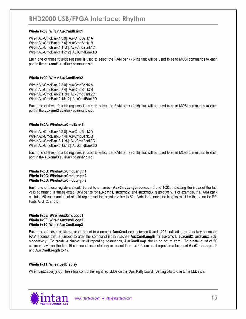
WireIn 0x08: WireInAuxCmdBank1 WireInAuxCmdBank1[3:0]: AuxCmdBank1A WireInAuxCmdBank1[7:4]: AuxCmdBank1B WireInAuxCmdBank1[11:8]: AuxCmdBank1C WireInAuxCmdBank1[15:12]: AuxCmdBank1D
Each one of these four-bit registers is used to select the RAM bank (0-15) that will be used to send MOSI commands to each port in the auxcmd1 auxiliary command slot.
WireIn 0x09: WireInAuxCmdBank2 WireInAuxCmdBank2[3:0]: AuxCmdBank2A WireInAuxCmdBank2[7:4]: AuxCmdBank2B WireInAuxCmdBank2[11:8]: AuxCmdBank2C WireInAuxCmdBank2[15:12]: AuxCmdBank2D
Each one of these four-bit registers is used to select the RAM bank (0-15) that will be used to send MOSI commands to each port in the auxcmd2 auxiliary command slot.
WireIn 0x0A: WireInAuxCmdBank3 WireInAuxCmdBank3[3:0]: AuxCmdBank3A WireInAuxCmdBank3[7:4]: AuxCmdBank3B WireInAuxCmdBank3[11:8]: AuxCmdBank3C WireInAuxCmdBank3[15:12]: AuxCmdBank3D
Each one of these four-bit registers is used to select the RAM bank (0-15) that will be used to send MOSI commands to each port in the auxcmd3 auxiliary command slot.
WireIn 0x0B: WireInAuxCmdLength1 WireIn 0x0C: WireInAuxCmdLength2 WireIn 0x0D: WireInAuxCmdLength3 Each one of these registers should be set to a number AuxCmdLength between 0 and 1023, indicating the index of the last valid command in the selected RAM banks for auxcmd1, auxcmd2, and auxcmd3, respectively. For example, if a RAM bank contains 60 commands that should repeat, set the register value to 59. Note that command lengths must be the same for SPI Ports A, B, C, and D.
WireIn 0x0E: WireInAuxCmdLoop1 WireIn 0x0F: WireInAuxCmdLoop2 WireIn 0x10: WireInAuxCmdLoop3 Each one of these registers should be set to a number AuxCmdLoop between 0 and 1023, indicating the auxiliary command RAM address that is jumped to after the command index reaches AuxCmdLength for auxcmd1, auxcmd2, and auxcmd3, respectively. To create a simple list of repeating commands, AuxCmdLoop should be set to zero. To create a list of 50 commands where the first 10 commands execute only once and the next 40 command repeat in a loop, set AuxCmdLoop to 9 and AuxCmdLength to 49.
WireIn 0x11: WireInLedDisplay WireInLedDisplay[7:0]: These bits control the eight red LEDs on the Opal Kelly board. Setting bits to one turns LEDs on.
RHD2000 USB/FPGA Interface: Rhythm
www.intantech.com ● [email protected] 16
intan TECHNOLOGIES, LLC
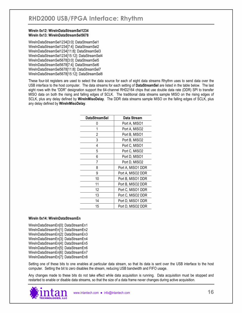
WireIn 0x12: WireInDataStreamSel1234 WireIn 0x13: WireInDataStreamSel5678 WireInDataStreamSel1234[3:0]: DataStreamSel1 WireInDataStreamSel1234[7:4]: DataStreamSel2 WireInDataStreamSel1234[11:8]: DataStreamSel3 WireInDataStreamSel1234[15:12]: DataStreamSel4 WireInDataStreamSel5678[3:0]: DataStreamSel5 WireInDataStreamSel5678[7:4]: DataStreamSel6 WireInDataStreamSel5678[11:8]: DataStreamSel7 WireInDataStreamSel5678[15:12]: DataStreamSel8
These four-bit registers are used to select the data source for each of eight data streams Rhythm uses to send data over the USB interface to the host computer. The data streams for each setting of DataStreamSel are listed in the table below. The last eight rows with the “DDR” designation support the 64-channel RHD2164 chips that use double data rate (DDR) SPI to transfer MISO data on both the rising and falling edges of SCLK. The traditional data streams sample MISO on the rising edges of SCLK, plus any delay defined by WireInMisoDelay. The DDR data streams sample MISO on the falling edges of SCLK, plus any delay defined by WireInMisoDelay.
DataStreamSel Data Stream 0 Port A, MISO1 1 Port A, MISO2 2 Port B, MISO1 3 Port B, MISO2 4 Port C, MISO1 5 Port C, MISO2 6 Port D, MISO1 7 Port D, MISO2 8 Port A, MISO1 DDR 9 Port A, MISO2 DDR
10 Port B, MISO1 DDR 11 Port B, MISO2 DDR 12 Port C, MISO1 DDR 13 Port C, MISO2 DDR 14 Port D, MISO1 DDR 15 Port D, MISO2 DDR
WireIn 0x14: WireInDataStreamEn WireInDataStreamEn[0]: DataStreamEn1 WireInDataStreamEn[1]: DataStreamEn2 WireInDataStreamEn[2]: DataStreamEn3 WireInDataStreamEn[3]: DataStreamEn4 WireInDataStreamEn[4]: DataStreamEn5 WireInDataStreamEn[5]: DataStreamEn6 WireInDataStreamEn[6]: DataStreamEn7 WireInDataStreamEn[7]: DataStreamEn8
Setting one of these bits to one enables at particular data stream, so that its data is sent over the USB interface to the host computer. Setting the bit to zero disables the stream, reducing USB bandwidth and FIFO usage.
Any changes made to these bits do not take effect while data acquisition is running. Data acquisition must be stopped and restarted to enable or disable data streams, so that the size of a data frame never changes during active acquisition.

RHD2000 USB/FPGA Interface: Rhythm
www.intantech.com ● [email protected] 17
intan TECHNOLOGIES, LLC
WireIn 0x15: WireInTtlOut This register sets the 16 TTL output pins defined by Rhythm. (If TTL_out_mode is set to one, the lower eight TTL output pins are controlled by the FPGA threshold comparators.)
WireIn 0x16: WireInDacSource1 WireIn 0x17: WireInDacSource2 WireIn 0x18: WireInDacSource3 WireIn 0x19: WireInDacSource4 WireIn 0x1A: WireInDacSource5 WireIn 0x1B: WireInDacSource6 WireIn 0x1C: WireInDacSource7 WireIn 0x1D: WireInDacSource8 WireInDacSourceX[4:0]: DacSourceChannelX WireInDacSourceX[8:5]: DacSourceStreamX WireInDacSourceX[9]: DacSourceEnableX
These registers route selected amplifier signals to the eight DACs that Rhythm supports. For each DAC, the user may select an amplifier channel (0-31) and a data stream (see table below). To enable the DAC, the DacSourceEnable bit must be set high. If DacSourceStream is set to 8, the DAC will be controlled directly by the host computer via WireInDacManual; the DacSourceChannel parameter is ignored in this case.
DacSourceStream Data Stream Routed to DAC 0 Data Stream 1 1 Data Stream 2 2 Data Stream 3 3 Data Stream 4 4 Data Stream 5 5 Data Stream 6 6 Data Stream 7 7 Data Stream 8 8 DAC Manual Input
10-15 all zeros
WireIn 0x1E: WireInDacManual This WireIn is used to control DACs directly when their DacSourceStream parameter is set to 8 (see table above). Typically, this WireIn can only be updated around 1,000 times per second in compiled C++ software, so it cannot be used to synthesize high-frequency waveforms.
WireIn 0x1F: WireInMultiUse WireInMultiUse is used in concert with TriggerIn signals to program other registers in the FPGA. (See below.)

RHD2000 USB/FPGA Interface: Rhythm
www.intantech.com ● [email protected] 18
intan TECHNOLOGIES, LLC
TrigIn 0x43: TrigInDacThresh TrigInDacThresh[0]: SetDac1ThresholdLevel TrigInDacThresh[1]: SetDac2ThresholdLevel TrigInDacThresh[2]: SetDac3ThresholdLevel TrigInDacThresh[3]: SetDac4ThresholdLevel TrigInDacThresh[4]: SetDac5ThresholdLevel TrigInDacThresh[5]: SetDac6ThresholdLevel TrigInDacThresh[6]: SetDac7ThresholdLevel TrigInDacThresh[7]: SetDac8ThresholdLevel
TrigInDacThresh[8]: SetDac1ThresholdPolarity TrigInDacThresh[9]: SetDac2ThresholdPolarity TrigInDacThresh[10]: SetDac3ThresholdPolarity TrigInDacThresh[11]: SetDac4ThresholdPolarity TrigInDacThresh[12]: SetDac5ThresholdPolarity TrigInDacThresh[13]: SetDac6ThresholdPolarity TrigInDacThresh[14]: SetDac7ThresholdPolarity TrigInDacThresh[15]: SetDac8ThresholdPolarity
Beginning in Version 1.3, Rhythm includes on-FPGA threshold comparators that produce low-latency digital signals indicating if each waveform routed to one of the eight DACs exceeded user-programmed levels. The bits in this TrigIn are used to program DAC threshold levels and polarities. To program a DAC threshold level, apply the desired value to WireInMultiUse and pulse one of the bottom eight bits in TrigInDacThresh.
To program a DAC threshold polarity, apply either a zero or one to WireInMultiUse and pulse one of the top eight bits in TrigInDacThresh. A polarity value of zero will cause the corresponding digital output to go high when the signal routed to that DAC equals or falls below the DAC threshold level. A polarity value of one will cause the digital output to go high when the signal routed to that DAC equals or rises above the DAC threshold level.
TrigIn 0x44: TrigInDacHpf TrigInDacHpf[0]: EnableDacHighpassFilter TrigInDacHpf[1]: SetDacHighpassFilterCutoff
Beginning in Version 1.3, Rhythm includes on-FPGA first-order high-pass filters that can be applied to the eight amplifier signals routed to the DACs and threshold comparators (see above). These high-pass filters can be used to remove low-frequency local field potentials (LFPs) from wideband neural signals before detecting spikes using the programmable comparators. The bits in this TrigIn are used to enable the high-pass filters and to program their cutoff frequency.
To enable or disable the high-pass filters, apply a one or zero, respectively, to WireInMultiUse and pulse TrigInDacHpf[0]. To set the filter cutoff frequency, apply the filter coefficient to WireInMultiUse and pulse TrigInDacHpf[1]. The filter coefficient is a 16-bit unsigned integer that is calculated as follows:
Filter coefficient = 65536 · [1 – exp(–2π·fcutoff/fsample)]
Note that the filter coefficient depends on the amplifier sampling frequency, so if this is changed, the filter coefficient should be updated appropriately.
TrigIn 0x45: TrigInExtFastSettle TrigInExtFastSettle[0]: EnableExternalFastSettle TrigInExtFastSettle[1]: SetExternalFastSettleChannel
Beginning in Version 1.4, Rhythm includes real-time control of the “fast settle” function on all connected RHD2000 chips. Enabling fast settle effectively blanks the amplifiers and prevents them from saturating during exposure to large transient input signals (e.g., due to nearby stimulation). To enable or disable real-time control of the fast settle function, apply a one or zero, respectively, to WireInMultiUse and pulse TrigInExtFastSettle[0]. To select the TTL digital input used for fast settle control,
RHD2000 USB/FPGA Interface: Rhythm
www.intantech.com ● [email protected] 19
intan TECHNOLOGIES, LLC
apply a number between 0 and 15 to WireInMultiUse and pulse TrigInExtFastSettle[1]. There is a latency of 4-5 amplifier sampling periods from the digital input changing to the fast settle function turning on or off.
TrigIn 0x46: TrigInExtDigOut TrigInExtDigOut[0]: EnableExternalDigOutPortA TrigInExtDigOut[1]: EnableExternalDigOutPortB TrigInExtDigOut[2]: EnableExternalDigOutPortC TrigInExtDigOut[3]: EnableExternalDigOutPortD TrigInExtDigOut[4]: SetExternalDigOutChannelPortA TrigInExtDigOut[5]: SetExternalDigOutChannelPortB TrigInExtDigOut[6]: SetExternalDigOutChannelPortC TrigInExtDigOut[7]: SetExternalDigOutChannelPortD
Beginning in Version 1.4, Rhythm includes real-time control of the auxiliary digital output pin (auxout) on each RHD2000 chip connected to the FPGA. To enable or disable real-time control of auxiliary digital output pins on Ports A, B, C, or D, apply a one or zero to WireInMultiUse and pulse one of TrigInExtDigOut[0-3]. To select the TTL digital input used for auxiliary digital output control, apply a number between 0 and 15 to WireInMultiUse and pulse one of TrigInExtDigOut [4-7]. There is a latency of 4-5 amplifier sampling periods from the digital input changing to the auxout pin on the RHD2000 chip turning on or off.
USB Software Endpoints: WireOut Ports WireOut ports are virtual 16-bit wires that transfer data asynchronously from the FPGA to the host computer. Up to 32 WireOut ports (with addresses from 0x20 to 0x3F) are available for use with each Opal Kelly module. The following C++ code shows how data is received from WireOut ports. okCFrontPanel *dev; // Code to open Opal Kelly board not shown here. // We must first execute UpdateWireOuts to refresh WireOut values on host computer. dev->UpdateWireOuts(); // Read from WireOut 0x20 endpoint. unsigned int fromFpga; fromFpga = dev->GetWireOutValue(0x20);
WireOut 0x20: WireOutNumWordsLsb WireOut 0x21: WireOutNumWordsMsb These two 16-bit ports are used to transfer a 32-bit unsigned integer NumWords that indicates the total number of 16-bit words contained in the USB FIFO on the Opal Kelly board. Before executing a ReadFromPipeOut command, the host computer should first read this number to ensure that sufficient data is present in the FIFO buffer. Otherwise, underflow will occur and corrupted data will be transferred to the computer. (Note that NumWords reports the number of 16-bit words in the FIFO, while ReadFromPipeOut operates at the byte level.) These ports should also be monitored to prevent buffer overflow. The FIFO can hold a bit over 226 = 67,108,864 words, but in practice it should never be allowed to get close to its maximum capacity.
WireOut 0x22: WireOutSpiRunning WireOutSpiRunning[0]: SpiRunning
This bit is high while data acquisition is running and low when it has stopped.
WireOutSpiRunning[15:1]: unused

RHD2000 USB/FPGA Interface: Rhythm
www.intantech.com ● [email protected] 20
intan TECHNOLOGIES, LLC
WireOut 0x23: WireOutTtlIn This register returns the values of the 16 TTL input pins defined by Rhythm. (These pins are also sampled synchronously with the RHD2000 amplifiers and reported in the main data stream, but this WireOut register provides a means for checking these pins asynchronously, or when SPI data acquisition is not running.)
WireOut 0x24: WireOutDataClkLocked WireOutDataClkLocked[0]: DataClkLocked
This bit goes high when the digital clock manager has successfully stabilized to a new frequency. When WireInDataFreqPll is changed and DcmProgTrigger is pulsed, it can take several milliseconds for the new clock frequency to stabilize. This pin should be monitored after frequency changes, and no data acquisition should be performed until this bit goes high.
WireOutDataClkLocked[1]: DcmProgDone
When WireInDataFreqPll is changed and DcmProgTrigger is pulsed, it can take several milliseconds before the digital clock manager is ready to be changed to yet another frequency. After any frequency changes this pin should be monitored, and no more frequency changes should be attempted until this bit goes high.
WireOutDataClkLocked[15:2]: unused
WireOut 0x3E: WireOutBoardId This WireOut returns a constant value of 500 (decimal), identifying the board as a Rhythm-compatible device.
WireOut 0x3F: WireOutBoardVersion This WireOut returns a constant value, identifying the version of Rhythm running on the board.
USB Software Endpoints: PipeOut Ports PipeOut ports are virtual 8-bit buses that stream data bytes synchronously from the FPGA to the host computer. Up to 32 PipeOut ports (with addresses from 0xA0 to 0xBF) are available for use with each Opal Kelly module. The following C++ code shows how data is streamed over PipeOut ports. okCFrontPanel *dev; // Code to open Opal Kelly board not shown here. // Allocate buffer to store 64 kBytes. unsigned char usbBuffer[65536]; // Read 64 kBytes from PipeOut 0xA0 into buffer. long numBytesRead, numBytesToRead; numBytesToRead = 65536; numBytesRead = dev->ReadFromPipeOut(0xA0, numBytesToRead, usbBuffer); // Note: numBytesRead will be negative if read failed. // 16-bit words are sent least-significant-byte first. unsigned int firstWord; firstWord = (usbBuffer[1] << 8) | usbBuffer[0];

RHD2000 USB/FPGA Interface: Rhythm
www.intantech.com ● [email protected] 21
intan TECHNOLOGIES, LLC
In order to minimize communication overhead and achieve maximum USB transfer speeds, Opal Kelly recommends reading from PipeOuts in relatively large data blocks. Reading at least 5 milliseconds of accumulated amplifier data from the board at a time will provide adequate USB data rates in most cases. See the Opal Kelly FrontPanel User’s Manual for more information.
PipeOut 0xA0: PipeOutData This PipeOut is used to stream data from all RHD2000 chips (and several additional data sources) through the FPGA to the host computer. The PipeOut is backed by a large FIFO implemented using the 128 MByte SDRAM on the Opal Kelly board. This FIFO module allows continuously-streaming data (e.g., from multiple RHD2000 chips to be transferred smoothly over a USB interface to a computer that will grab the data in bursts, and may be unresponsive for a brief time due to multitasking or other operating system overhead.
There is no mechanism in this FIFO to protect against underflow. That is, if the computer tries to read more data than the FIFO is currently holding, the FIFO will just repeat the last word after it runs out of data. To prevent underflow, it is essential for the host to monitor the value of NumWords (WireOut 0x20 and 0x21) and never attempt to read more words than the FIFO contains.
Example: okCFrontPanel *dev; // Code to open Opal Kelly board and start SPI operation not shown here. // Allocate buffer to store data. unsigned char usbBuffer[BUFFERSIZE]; // Wait until enough data is available in the FIFO... unsigned int numWordsAvailable = 0; while (numWordsAvailable < BUFFERSIZE / 2) { dev->UpdateWireOuts(); numWordsAvailable = 65536 * dev->GetWireOutValue(0x21) + dev->GetWireOutValue(0x20); } // Remember, NumWords (WireOut 0x20 and 0x21) returns the number of 16-bit words in // the FIFO, but ReadFromPipeOut() operates on bytes. Factor of two difference! // Read bytes from PipeOut 0xA0 into buffer. long numBytesRead; numBytesRead = dev->ReadFromPipeOut(0xA0, BUFFERSIZE, usbBuffer);

RHD2000 USB/FPGA Interface: Rhythm
www.intantech.com ● [email protected] 22
intan TECHNOLOGIES, LLC
Rhythm Verilog Code Description Verilog Source Code The Rhythm interface is described by a set of Verilog files that may be compiled into a bitfile using the free Xilinx ISE WebPack software. While Intan Technologies provides a pre-compiled bitfile, developers may wish to modify the Rhythm code for custom applications. The primary Verilog files are described below.
main.v: This is the top-level Rhythm Verilog code that defines all FPGA I/O, executes the main state machine running all SPI I/O with the RHD2000 chips, and defines connections to all other modules in the Verilog files listed below.
SDRAM_FIFO.v: This code makes use of the off-FPGA 128-MByte SDRAM to implement a large FIFO buffer. This Verilog file uses a number of other miscellaneous Verilog files to implement the SDRAM controller. Many of these files were derived from the Opal Kelly RamTest Verilog example.
variable_freq_clk_generator.v: This module sets up the programmable-frequency clock used to run the RHD2000 chips at user-selectable sampling rates.
MISO_phase_selector.v: This small module implements the user-programmable delay in sampling MISO SPI lines to compensate for signal propagation delay on long cables.
RAM_bank.v and RAM_block.v: These files use on-FPGA memory to implement multiple 1024-word RAM banks for storing auxiliary command sequences.
DAC_output_scalable.v: This module implements a serial interface to an optional off-board Analog Devices AD5662 16-bit DAC, as well as variable gain, noise slicing, high-pass filtering, and threshold comparator functions.
ADC_input.v: This module implements a serial interface to an optional off-board Analog Devices AD7680 16-bit ADC.
okLibrary.v: This Verilog file provided by Opal Kelly implements the communication endpoints (e.g., WireIns, PipeOuts) in the FPGA. It should not be modified.
xem6010.ucf: This file defines the location (i.e., pin number) and characteristics (i.e., LVDS) of all FPGA I/O signals.
main.bit: This is the bitfile that is generated by compiling all the above Verilog files with Xilinx ISE WebPack. This file should be copied into the directory containing the C++ executable file that opens and configures the Opal Kelly board.
Note: During compilation, users will see there is one failing timing constraint related to the following lines in xem6010.ucf: NET "SDRAM_FIFO_inst/memc3_infrastructure_inst/sys_clk_ibufg" TNM_NET = "SYS_CLK3"; TIMESPEC "TS_SYS_CLK3" = PERIOD "SYS_CLK3" 10 ns HIGH 50 %;
These constraints were inherited from the Opal Kelly RamTest Verilog demo, and they have not been changed. The failing timing constraint does not seem to affect FPGA operation.
RHD2000 USB/FPGA Interface: Rhythm
www.intantech.com ● [email protected] 23
intan TECHNOLOGIES, LLC
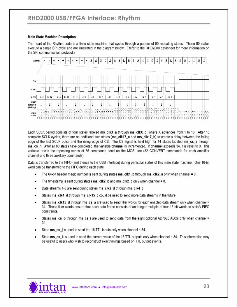
Main State Machine Description The heart of the Rhythm code is a finite state machine that cycles through a pattern of 80 repeating states. These 80 states execute a single SPI cycle and are illustrated in the diagram below. (Refer to the RHD2000 datasheet for more information on the SPI communication protocol.)
Each SCLK period consists of four states labeled ms_clkX_a through ms_clkX_d, where X advances from 1 to 16. After 16 complete SCLK cycles, there are an additional two states (ms_clk17_a and ms_clk17_b) to create a delay between the falling edge of the last SCLK pulse and the rising edge of CS. The CS signal is held high for 14 states labeled ms_cs_a through ms_cs_n. After all 80 states have completed, the variable channel is incremented. If channel exceeds 34, it is reset to 0. This variable tracks the repeating series of 35 commands send on the MOSI line (32 CONVERT commands for each amplifier channel and three auxiliary commands).
Data is transferred to the FIFO (and thence to the USB interface) during particular states of this main state machine. One 16-bit word can be transferred to the FIFO during each state.
• The 64-bit header magic number is sent during states ms_clk1_b through ms_clk2_a only when channel = 0.
• The timestamp is sent during states ms_clk2_b and ms_clk2_c only when channel = 0.
• Data streams 1-8 are sent during states ms_clk2_d through ms_clk4_c.
• States ms_clk4_d through ms_clk15_c could be used to send more data streams in the future.
• States ms_clk15_d through ms_cs_a are used to send filler words for each enabled data stream only when channel = 34. These filler words ensure that each data frame consists of an integer multiple of four 16-bit words to satisfy FIFO constraints.
• States ms_cs_b through ms_cs_i are used to send data from the eight optional AD7680 ADCs only when channel = 34.
• State ms_cs_j is used to send the 16 TTL inputs only when channel = 34.
• State ms_cs_k is used to send the current value of the 16 TTL outputs only when channel = 34. This information may be useful to users who wish to reconstruct exact timings based on TTL output events.
RHD2000 USB/FPGA Interface: Rhythm
www.intantech.com ● [email protected] 24
intan TECHNOLOGIES, LLC
Rhythm C++ API Intan Technologies provides a basic, open-source C++ application programming interface (API) for controlling the Rhythm FPGA interface described above. The API consists of three C++ classes: Rhd2000EvalBoard, Rhd2000Registers, and Rhd2000DataBlock. These classes are defined in *.cpp and *.h files named rhd2000evalboard, rhd2000registers, and rhd2000datablock. Additionally, any application must include the Opal Kelly API files okFrontPanelDLL.cpp and okFrontPanelDLL.h.
The Rhythm API is written using standard C++ and uses the string, vector, and queue classes from the C++ Standard Template Library (STL).
The public member functions of each class in the Rhythm API are described below.
Rhd2000EvalBoard Class Reference This class provides access to and control of the Opal Kelly XEM6010 USB/FPGA interface board running the Rhythm interface Verilog code. Only one instance of the Rhd2000EvalBoard object is needed to control a Rhythm-based FPGA interface.
The public member functions of the Rhd2000EvalBoard class are listed below.
Rhd2000EvalBoard() Constructor.
int open() Finds an Opal Kelly XEM6010-LX45 board attached to a USB port and opens it. Returns 1 if successful. Returns -1 if Opal Kelly FrontPanel DLL cannot be loaded. Returns -2 if an XEM6010 board is not found.
bool uploadFpgaBitFile(string filename) Uploads the Rhythm configuration file (i.e., bitfile) to the Xilinx FPGA on the open Opal Kelly board. Returns true if successful.
void initialize() Initializes Rhythm FPGA registers to default values.
void resetBoard() Resets the FPGA. This clears all auxiliary command RAM banks, clears the USB FIFO, and resets the per-channel sampling rate to its default value of 30.0 kS/s/channel.
bool setSampleRate(AmplifierSampleRate newSampleRate) Sets the per-channel sampling rate of the RHD2000 chips connected to the Rhythm FPGA. Returns false if an unsupported sampling rate is requested. Sample rates are given using the AmplifierSampleRate enumeration; defined values are:
SampleRate1000Hz SampleRate1250Hz SampleRate1500Hz SampleRate2000Hz SampleRate2500Hz SampleRate3000Hz

RHD2000 USB/FPGA Interface: Rhythm
www.intantech.com ● [email protected] 25
intan TECHNOLOGIES, LLC
SampleRate3333Hz SampleRate4000Hz SampleRate5000Hz SampleRate6250Hz SampleRate8000Hz SampleRate10000Hz SampleRate12500Hz SampleRate15000Hz SampleRate20000Hz SampleRate25000Hz SampleRate30000Hz
double getSampleRate() Returns the current per-channel sampling rate (in Hz) as a floating-point number.
AmplifierSampleRate getSampleRateEnum() Returns the current per-channel sampling rate as an AmplifierSampleRate enumeration.
void uploadCommandList(const vector<int> &commandList, AuxCmdSlot auxCommandSlot, int bank) Uploads a command list (generated by an instance of the Rhd2000Registers class) to a particular auxiliary command slot and RAM bank (0-15) on the FPGA. Command slots are given using the AuxCmdSlot enumeration; defined values are:
AuxCmd1 AuxCmd2 AuxCmd3
void printCommandList(const vector<int> &commandList) Prints a command list (generated by an instance of the Rhd2000Registers class) to the console in readable form, for diagnostic purposes.
void selectAuxCommandBank(BoardPort port, AuxCmdSlot auxCommandSlot, int bank) Selects an auxiliary command slot (AuxCmd1, AuxCmd2, or AuxCmd3) and bank (0-15) for a particular SPI port. The SPI port is specified using the BoardPort enumeration; defined values are:
PortA PortB PortC PortD
void selectAuxCommandLength(int auxCommandSlot, AuxCmdSlot loopIndex, int endIndex) Specifies a command sequence end point (endIndex = 0-1023) and command loop index (loopIndex = 0-1023) for a particular auxiliary command slot (AuxCmd1, AuxCmd2, or AuxCmd3).
void setContinuousRunMode(bool continuousMode); Sets the FPGA to run continuously once started (if continuousMode is set to true) or to run until maxTimeStep is reached (if continuousMode is set to false).

RHD2000 USB/FPGA Interface: Rhythm
www.intantech.com ● [email protected] 26
intan TECHNOLOGIES, LLC
void setMaxTimeStep(unsigned int maxTimeStep) Sets maxTimeStep for cases where continuousMode = false.
void run() Starts SPI data acquisition.
bool isRunning() Returns true if the FPGA is currently running SPI data acquisition.
unsigned int numWordsInFifo() Returns the number of 16-bit words in the USB FIFO. The user should never attempt to read more data than the FIFO currently contains, as it is not protected against underflow.
unsigned int fifoCapacityInWords() Returns the number of 16-bit words in the USB SDRAM FIFO can hold (67,108,864). The FIFO can actually hold a few thousand words more than this due to the on-FPGA mini-FIFOs used to interface with the SDRAM, but this function provides a conservative estimate of maximum FIFO capacity.
void setCableDelay(BoardPort port, int delay) Sets the delay for sampling the MISO line on a particular SPI port (PortA, PortB, PortC, or PortD), in integer clock steps, where each clock step is 1/2800 of a per-channel sampling period. Cable delay should be updated after any changes are made to the sampling rate, since cable delay calculations are based on the clock period.
Most users will probably find it more convenient to use setCableLengthMeters or setCableLengthFeet instead of using setCableDelay directly.
int getCableDelay(BoardPort port) void getCableDelay(vector<int> &delays) Returns the last delay set on a particular SPI port (PortA, PortB, PortC, or PortD), or all ports, in integer clock steps.
void setCableLengthMeters(BoardPort port, double lengthInMeters) void setCableLengthFeet(BoardPort port, double lengthInFeet)
Sets the delay for sampling the MISO line on a particular SPI port (PortA, PortB, PortC, or PortD) based on the length of the cable between the FPGA and the RHD2000 chip (in meters or feet). Cable delay should be updated after any changes are made to the sampling rate, since cable delay calculations are based on the clock period.
double estimateCableLengthMeters(int delay) double estimateCableLengthFeet(int delay)
Based on a delay setting used in setCableDelay, these functions return the estimated cable length corresponding to this setting.

RHD2000 USB/FPGA Interface: Rhythm
www.intantech.com ● [email protected] 27
intan TECHNOLOGIES, LLC
void setDspSettle(bool enabled); Turns on or off the DSP settle function in the FPGA. (This only executes when CONVERT commands are executed by the RHD2000.)
void setDataSource(int stream, BoardDataSource dataSource) Assigns a particular data source to one of the eight available USB data streams (0-7). The data source is specified using the BoardDataSource enumeration; defined values are:
PortA1 PortA2 PortB1 PortB2 PortC1 PortC2 PortD1 PortD2 PortA1Ddr PortA2Ddr PortB1Ddr PortB2Ddr PortC1Ddr PortC2Ddr PortD1Ddr PortD2Ddr
The DDR (double data rate) sources are included to support 64-channel RHD2164 chips that return MISO data on both the rising and falling edges of SCLK. See the RHD2164 datasheet for more details.
void enableDataStream(int stream, bool enabled) Enables (if enabled is true) or disables (if enabled is false) one of the eight available USB data streams (0-7).
int getNumEnabledDataStreams() Returns the total number of enabled USB data streams.
void clearTtlOut() Sets all 16 bits of the digital TTL output lines on the FPGA to zero.
void setTtlOut(int ttlOutArray[]) Sets the 16 bits of the digital TTL output lines on the FPGA high or low according to an integer array. The length-16 array ttlOutArray should contain values of 0 or 1.
void getTtlIn(int ttlInArray[]) Reads the 16 bits of the digital TTL input lines on the FPGA into a length-16 integer array.
void setDacManual(int value) Sets the manual AD5662 DAC control (DacManual) WireIn to value (0-65536).

RHD2000 USB/FPGA Interface: Rhythm
www.intantech.com ● [email protected] 28
intan TECHNOLOGIES, LLC
void setLedDisplay(int ledArray[]) Sets the eight red LEDs on the Opal Kelly XEM6010 board according to a length-8 integer array.
void enableDac(int dacChannel, bool enabled) Enables (if enabled is true) or disables (if enabled is false) AD5662 DACs connected to the FPGA.
void setDacGain(int gain) Scales the digital signals to all eight AD5662 DACs by a factor of 2gain, where gain is between 0 and 7.
void setAudioNoiseSuppress(int noiseSuppress) Sets the noise slicing region for DAC channels 1 and 2 (i.e., audio left and right) to +/-16 x noiseSuppress LSBs, where noiseSuppress is between 0 and 127. This improves the audibility of weak neural spikes in noisy waveforms.
void selectDacDataStream(int dacChannel, int stream) void selectDacDataChannel(int dacChannel, int dataChannel)
Assigns a particular data stream (0-7) and amplifier channel (0-31) to an AD5662 DAC channel (0-7). Setting stream to 8 selects the DacManual source.
void enableDacHighpassFilter(bool enable) Enables (if enabled is true) or disables (if enabled is false) the first-order high-pass filters implemented in the FPGA on all eight DAC/comparator channels. These filters may be used to remove low-frequency local field potential (LFP) signals from neural signals to facilitate spike detection while still recording the complete wideband data.
void setDacHighpassFilter(double cutoff) Sets a cutoff frequency (in Hz) for first-order high-pass filters implemented in the FPGA on all eight DAC/comparator channels.
void setDacThreshold(int dacChannel, int threshold, bool trigPolarity) Sets a threshold level (0-65535) and trigger polarity for a low-latency FPGA threshold comparator on a DAC channel (0-7). The threshold parameter corresponds to the RHD2000 chip ADC output value, where the ‘zero’ level is 32768 and the step size is 0.195 μV. If the trigger polarity is set to true, RHD2000 signals equaling or rising above the threshold produce a high digital output. If the trigger polarity is set to false, RHD2000 signals equaling for falling below the threshold produce a high digital output. If the corresponding DAC is disabled, the digital output will always be low.
To enable the comparator output signals on TTL outputs 0-7, the setTtlMode function must be used (see below).
void setTtlMode(int mode) Sets the TTL digital output mode of the FPGA. If mode is set to zero, all 16 TTL digital output pins are controlled manually using setTtlOut. If mode is set to one, the upper eight TTL outputs are controlled manually, while the lower eight TTL outputs are controlled by low-latency threshold comparators connected to the eight waveforms routed to the DACs.

RHD2000 USB/FPGA Interface: Rhythm
www.intantech.com ● [email protected] 29
intan TECHNOLOGIES, LLC
void enableExternalFastSettle(bool enable) Enables or disables real-time control of amplifier fast settle from an external digital input.
void setExternalFastSettleChannel(int channel) Selects external TTL digital input channel (0-15) used to control amplifier fast settle function.
void enableExternalDigOut(BoardPort port, bool enable) Enables or disables real-time control of auxiliary digital output pin (auxout) on RHD2000 chips on a selected SPI port from an external digital input.
void setExternalDigOutChannel(BoardPort port, int channel) Selects external TTL digital input channel (0-15) used to control the auxiliary digital output pin (auxout) on RHD2000 chips on a selected SPI port.
void flush() Flush all remaining data out of the FIFO. (This function should only be called when SPI data acquisition has been stopped.)
int readDataBlock(Rhd2000DataBlock *dataBlock) Reads a data block from the USB interface and stores the data into an Rhd2000DataBlock object dataBlock.
bool readDataBlocks(int numBlocks, queue<Rhd2000DataBlock> &dataQueue) Reads a specified number of data blocks from the USB interface and appends them to a queue. Returns true if the requested number of data blocks were available. New in version 1.5: Checks headers for proper USB data synchrony and corrects alignment if any bytes have been dropped by the USB interface.
int queueToFile(queue<Rhd2000DataBlock> &dataQueue, ofstream &saveOut) Writes the contents of a data block queue to a binary output stream. Returns number of data blocks appended to queue.
int getBoardMode() Reads four digital input pins on the FPGA (see JP3 I/O Connections section) and returns this as an integer. These pins will typically be hard-wired either high or low to encode a 4-bit number that identifies particular properties of the interface board.
Rhd2000Registers Class Reference This class creates and manages a data structure representing the internal RAM registers on a RHD2000 chip, and generates command lists to configure the chip and perform other functions. Changing the value of variables within an instance of this class does not directly affect a RHD2000 chip connected to the FPGA; rather, a command list must be generated from this class and then downloaded to the FPGA board using Rhd2000EvalBoard::uploadCommandList. Typically, one instance of Rhd2000Registers will be created for each RHD2000 chip attached to the Rhythm interface. However, if all chips will receive the same MOSI commands, then only one instance of Rhd2000Registers is required.
The public member functions of the Rhd2000Registers class are listed below.
RHD2000 USB/FPGA Interface: Rhythm
www.intantech.com ● [email protected] 30
intan TECHNOLOGIES, LLC
Rhd2000Registers(double sampleRate) Constructor. Sets RHD2000 register variables to default values.
void defineSampleRate(double newSampleRate) Defines RHD2000 per-channel sampling rate so that certain sample-rate-dependent registers are set correctly. (This function does not change the sampling rate of the FPGA; for this, use Rhd2000EvalBoard::setSampleRate.)
void setFastSettle(bool enabled) Enables or disables amplifier fast settle function.
void setDigOutLow() void setDigOutHigh() void setDigiOutHiZ()
Sets the auxiliary digital output variable to indicate a low, high, or high impedance (HiZ) output.
void enableAux1(bool enabled) void enableAux2(bool enabled) void enableAux3(bool enabled)
Enables or disables ADC auxiliary inputs 1, 2, and 3.
void enableDsp(bool enabled) Enables or disables DSP offset removal filter.
double setDspCutoffFreq(double newDspCutoffFreq) Sets the DSP offset removal filter cutoff frequency as closely to the requested newDspCutoffFreq (in Hz) as possible; returns the actual cutoff frequency (in Hz).
double getDspCutoffFreq() Returns the current value of the DSP offset removal cutoff frequency (in Hz).
void enableZcheck(bool enabled) Enables or disables impedance checking mode.
void setZcheckDacPower(bool enabled) Powers up or down impedance testing DAC.

RHD2000 USB/FPGA Interface: Rhythm
www.intantech.com ● [email protected] 31
intan TECHNOLOGIES, LLC
void setZcheckScale(ZcheckCs scale) Selects the series capacitor CS used to convert the voltage waveform generated by the on-chip DAC into an AC current waveform that stimulates a selected electrode for impedance testing. The capacitor is specified using the ZCheckCs enumeration; defined values are:
ZcheckCs100fF ZcheckCs1pF ZcheckCs10pF
void setZcheckPolarity(ZcheckPolarity polarity) Selects impedance testing of positive or negative amplifier inputs (RHD2216 only), specified using the ZcheckPolarity enumeration; defined values are:
ZcheckPositiveInput ZcheckNegativeInput
int setZcheckChannel(int channel) Selects the amplifier channel (0-63) for impedance testing.
void setAmpPowered(int channel, bool powered) void powerUpAllAmps() void powerDownAllAmps()
Powers up or down selected amplifiers on RHD2000 chip.
int getRegisterValue(int reg) Returns the value of a selected RHD2000 RAM register (0-17), based on the current register variables in the class instance.
double setUpperBandwidth(double upperBandwidth) double setLowerBandwidth(double lowerBandwidth)
Sets the on-chip RH1, RH2, and RL DAC values appropriately to set a particular amplifier bandwidth (in Hz). Returns an estimate of the actual bandwidth achieved.
int createRhd2000Command(Rhd2000CommandType commandType) int createRhd2000Command(Rhd2000CommandType commandType, int arg1) int createRhd2000Command(Rhd2000CommandType commandType, int arg1, int arg2)
Returns a 16-bit MOSI command based on the Rhd2000CommandType enumeration; defined values are:
Rhd2000CommandConvert Rhd2000CommandCalibrate Rhd2000CommandCalClear Rhd2000CommandRegWrite Rhd2000CommandRegRead
CONVERT and READ commands use arg1 to specify a register or channel; WRITE commands use arg1 and arg2 to specify a register and value, respectively.

RHD2000 USB/FPGA Interface: Rhythm
www.intantech.com ● [email protected] 32
intan TECHNOLOGIES, LLC
int createCommandListRegisterConfig(vector<int> &commandList, bool calibrate) Creates a list of 60 commands to program most RAM registers on a RHD2000 chip, read those values back to confirm programming, read ROM registers, and (if calibrate = true) run ADC calibration. Returns the length of the command list.
int createCommandListTempSensor(vector<int> &commandList) Creates a list of 60 commands to sample auxiliary ADC inputs, temperature sensor, and supply voltage sensor. One temperature reading (one sample of ResultA and one sample of ResultB) is taken during this 60-command sequence. One supply voltage sample is taken. Auxiliary ADC inputs are continuously sampled at 1/4 the amplifier sampling rate.
Since this command list consists of writing to Register 3, it also sets the state of the auxiliary digital output. If the digital output value needs to be changed dynamically, then variations of this command list need to be generated for each state and programmed into different RAM banks, and the appropriate command list selected at the right time.
Returns the length of the command list.
int createCommandListZcheckDac(vector<int> &commandList, double frequency, double amplitude) Creates a list of up to 1024 commands to generate a sine wave of particular frequency (in Hz) and amplitude (in DAC steps, 0-128) using the on-chip impedance testing voltage DAC. If frequency is set to zero, a DC baseline waveform is created, which can be used when impedance testing is disabled to minimize on-chip noise. This function returns the length of the command list.
int createCommandListUpdateDigOut(vector<int> &commandList) Creates a list of 60 commands to update Register 3 (controlling the auxiliary digital output pin) every sampling period. Since this command list consists of writing to Register 3, it also sets the state of the on-chip temperature sensor. The temperature sensor settings are therefore changed throughout this command list to coordinate with the 60-command list generated by createCommandListTempSensor(). This function returns the length of the command list.

RHD2000 USB/FPGA Interface: Rhythm
www.intantech.com ● [email protected] 33
intan TECHNOLOGIES, LLC
Rhd2000DataBlock Class Reference This class creates a data structure storing SAMPLES_PER_DATA_BLOCK data samples from a Rhythm FPGA interface controlling up to eight RHD2000 chips. (A #define statement in rhd2000datablock.h currently sets SAMPLES_PER_DATA_BLOCK to 60.) Typically, instances of Rhd2000DataBlock will be created dynamically as data becomes available over the USB interface and appended to a queue that will be used to stream the data to disk or to a GUI display.
The public member functions of the Rhd2000DataBlock class are listed below.
Rhd2000DataBlock(int numDataStreams) Constructor. Allocates memory for a data block supporting the specified number of data streams.
unsigned int getSamplesPerDataBlock() Returns the SAMPLES_PER_DATA_BLOCK, which is set to 60.
unsigned int calculateDataBlockSizeInWords(int numDataStreams) Returns the size of a USB data block (in 16-bit words) when numDataStreams data streams (0-7) are enabled.
void fillFromUsbBuffer(unsigned char usbBuffer[], int blockIndex, int numDataStreams) Fills the data block with raw data from the nth data block in a USB input buffer in an Rhd2000EvalBoard object. Setting blockIndex to 0 selects the first data block in the buffer, setting blockIndex to 1 selects the second data block, etc.
void print(int stream) Prints the contents of RHD2000 registers from a selected USB data stream (0-7) to the console. This function assumes that the command string generated by Rhd2000Registers::createCommandListRegisterConfig has been uploaded to the AuxCmd3 slot.
void write(ofstream &saveOut, int numDataStreams) Writes the contents of a data block object to a binary output stream in little endian format (i.e., least significant byte first).
bool checkUsbHeader(unsigned char usbBuffer[], int index)
Checks the first 64 bits of USB header against the fixed Rhythm “magic number” to verify proper data synchrony.

RHD2000 USB/FPGA Interface: Rhythm
www.intantech.com ● [email protected] 34
intan TECHNOLOGIES, LLC
Example Usage A simple main.cpp C++ program presented below opens an Opal Kelly XEM6010 board, configures it with the Rhythm FPGA configuration bitfile (main.bit), and sets the clock generator for a 20 kS/s/channel sampling rate. The MISO sampling delay is set for a 3-foot cable. The program then modifies the default values of the RHD2000 registers, generates command sequences for the three auxiliary command slots, and uploads these commands to the FPGA RAM banks. Two versions of the AuxCmd3 sequence are created: one runs the ADC calibration, and this is executed once in a 60-sample SPI run. Register data from this brief run is read over the USB interface, and displayed on the console to confirm RHD2000 register settings.
The other version of the AuxCmd3 sequence does not execute ADC calibration, so this RAM bank is used for the next acquisition, which is a one-second run. Complete data from the one-second acquisition is then saved in binary format to a file on disk.
#include <iostream> #include <fstream> #include <vector> #include <queue> using namespace std; #include "okFrontPanelDLL.h" #include "rhd2000evalboard.h" #include "rhd2000registers.h" #include "rhd2000datablock.h" int main(int argc, char *argv[]) { // Open Opal Kelly XEM6010 board, load Rhythm bitfile, and initialize. Rhd2000EvalBoard *evalBoard = new Rhd2000EvalBoard; evalBoard->open(); evalBoard->uploadFpgaBitfile("main.bit"); evalBoard->initialize(); evalBoard->setDataSource(0, Rhd2000EvalBoard::PortA1); // Select a per-amplifier sampling rate. evalBoard->setSampleRate(Rhd2000EvalBoard::SampleRate20000Hz); // Now that we have set our sampling rate, we can set the MISO sampling delay // which is dependent on the sample rate. We assume a 3-foot cable. evalBoard->setCableLengthFeet(Rhd2000EvalBoard::PortA, 3.0); // Let's turn one LED on to indicate that the program is running. int ledArray[8] = {1, 0, 0, 0, 0, 0, 0, 0}; evalBoard->setLedDisplay(ledArray); // Set up an RHD2000 register object using this sample rate. Rhd2000Registers *chipRegisters; chipRegisters = new Rhd2000Registers(evalBoard->getSampleRate()); // Create command lists to be uploaded to auxiliary command slots. int commandSequenceLength; vector<int> commandList; // First, let's create a command list for the AuxCmd1 slot. This command // sequence will create a 1 kHz, full-scale sine wave for impedance testing. commandSequenceLength = chipRegisters->createCommandListZcheckDac(commandList, 1000.0, 128.0); evalBoard->uploadCommandList(commandList, Rhd2000EvalBoard::AuxCmd1, 0); evalBoard->selectAuxCommandLength(Rhd2000EvalBoard::AuxCmd1, 0, commandSequenceLength - 1);

RHD2000 USB/FPGA Interface: Rhythm
www.intantech.com ● [email protected] 35
intan TECHNOLOGIES, LLC
evalBoard->selectAuxCommandBank(Rhd2000EvalBoard::PortA, Rhd2000EvalBoard::AuxCmd1, 0); // evalBoard->printCommandList(commandList); // optionally, print command list // Next, we'll create a command list for the AuxCmd2 slot. This command sequence // will sample the temperature sensor and other auxiliary ADC inputs. commandSequenceLength = chipRegisters->createCommandListTempSensor(commandList); evalBoard->uploadCommandList(commandList, Rhd2000EvalBoard::AuxCmd2, 0); evalBoard->selectAuxCommandLength(Rhd2000EvalBoard::AuxCmd2, 0, commandSequenceLength - 1); evalBoard->selectAuxCommandBank(Rhd2000EvalBoard::PortA, Rhd2000EvalBoard::AuxCmd2, 0); // evalBoard->printCommandList(commandList); // optionally, print command list // For the AuxCmd3 slot, we will create two command sequences. Both sequences // will configure and read back the RHD2000 chip registers, but one sequence will // also run ADC calibration. // Before generating register configuration command sequences, set amplifier // bandwidth paramters. double dspCutoffFreq; dspCutoffFreq = chipRegisters->setDspCutoffFreq(10.0); // 10 Hz DSP cutoff cout << "Actual DSP cutoff frequency: " << dspCutoffFreq << " Hz" << endl; chipRegisters->setLowerBandwidth(1.0); // 1.0 Hz lower bandwidth chipRegisters->setUpperBandwidth(7500.0); // 7.5 kHz upper bandwidth commandSequenceLength = chipRegisters->createCommandListRegisterConfig(commandList, false); // Upload version with no ADC calibration to AuxCmd3 RAM Bank 0. evalBoard->uploadCommandList(commandList, Rhd2000EvalBoard::AuxCmd3, 0); chipRegisters->createCommandListRegisterConfig(commandList, true); // Upload version with ADC calibration to AuxCmd3 RAM Bank 1. evalBoard->uploadCommandList(commandList, Rhd2000EvalBoard::AuxCmd3, 1); evalBoard->selectAuxCommandLength(Rhd2000EvalBoard::AuxCmd3, 0, commandSequenceLength - 1); // Select RAM Bank 1 for AuxCmd3 initially, so the ADC is calibrated. evalBoard->selectAuxCommandBank(Rhd2000EvalBoard::PortA, Rhd2000EvalBoard::AuxCmd3, 1); // evalBoard->printCommandList(commandList); // optionally, print command list // Since our longest command sequence is 60 commands, let’s just run the SPI // interface for 60 samples. evalBoard->setMaxTimeStep(60); evalBoard->setContinuousRunMode(false); // Start SPI interface. evalBoard->run(); // Wait for the 60-sample run to complete. while (evalBoard->isRunning()) { } // Read the resulting single data block from the USB interface. Rhd2000DataBlock *dataBlock = new Rhd2000DataBlock(evalBoard->getNumEnabledDataStreams()); evalBoard->readDataBlock(dataBlock); // Display register contents from data stream 0. dataBlock->print(0); // Now that ADC calibration has been performed, we switch to the command sequence // that does not execute ADC calibration.

RHD2000 USB/FPGA Interface: Rhythm
www.intantech.com ● [email protected] 36
intan TECHNOLOGIES, LLC
evalBoard->selectAuxCommandBank(Rhd2000EvalBoard::PortA, Rhd2000EvalBoard::AuxCmd3, 0); // Let's save one second of data to a binary file on disk. ofstream saveOut; saveOut.open("binary_save_file.dat", ios::binary | ios::out); queue<Rhd2000DataBlock> dataQueue; // Run for one second. evalBoard->setMaxTimeStep(20000); evalBoard->run(); bool usbDataRead; do { usbDataRead = evalBoard->readDataBlocks(1, dataQueue); if (dataQueue.size() >= 50) { // save 50 data blocks at a time evalBoard->queueToFile(dataQueue, saveOut); } } while (usbDataRead || evalBoard->isRunning()); evalBoard->queueToFile(dataQueue, saveOut); saveOut.close(); // Turn off LED. ledArray[0] = 0; evalBoard->setLedDisplay(ledArray); }
An elaborated version of this main.cpp program file is included with the Rhythm API distribution files.

RHD2000 USB/FPGA Interface: Rhythm
www.intantech.com ● [email protected] 37
intan TECHNOLOGIES, LLC
Reading binary data into MATLAB The C++ program above saves data from a single data stream to a binary output file. The following MATLAB code reads a saved file for the case where only one data stream is active:
fid = fopen(filename, 'r'); s = dir(filename); filesize = s.bytes; % allocate space to read the entire file data = zeros(filesize, 1, 'uint8'); % read the entire file data = fread(fid, filesize, 'uint8=>uint8'); fclose(fid); % convert the remaining data from bytes to 2-byte unsigned integers data = typecast(data, 'uint16'); swapbytes(data); % convert uint16 datatype to double datatype data = double(data); L = length(data); data = reshape(data, 46, L/46); timestamp = data(1,:)'; amplifier_data = data(2:33,:)'; auxiliary_data = data(34:36,:)'; boardADC_data = data(37:44,:)'; TTLin = data(45,:)'; TTLout = data(46,:)';

RHD2000 USB/FPGA Interface: Rhythm
www.intantech.com ● [email protected] 38
intan TECHNOLOGIES, LLC
Contact Information This datasheet is meant to acquaint engineers and scientists with the Rhythm USB/FPGA interface code developed at Intan Technologies. We value feedback from potential end users. We can discuss your specific needs and suggest a solution tailored to your applications.
For more information, contact Intan Technologies at:
www.intantech.com [email protected]
© 2013-2016 Intan Technologies, LLC Information furnished by Intan Technologies is believed to be accurate and reliable. However, no responsibility is assumed by Intan Technologies for its use, nor for any infringements of patents or other rights of third parties that may result from its use. Specifications subject to change without notice. Intan Technologies assumes no liability for applications assistance or customer product design. Customers are responsible for their products and applications using Intan Technologies components. To minimize the risks associated with customer products and applications, customers should provide adequate design and operating safeguards.
Intan Technologies’ products are not authorized for use as critical components in life support devices or systems. A critical component is any component of a life support device or system whose failure to perform can be reasonably expected to cause the failure of the life support device or system, or to affect its safety or effectiveness.
intan TECHNOLOGIES, LLC