Embed Size (px)
Citation preview
RJ-11/13 Application Note Ver 1.0 COMPANY CONFIDENTIAL
Copyright @ RJ Electronics. All rights reserved. 1 / 103
RJ-11/13
APPLICATION NOTE APPLICATION NOTE Ver 1.0
RJ-11/13
Document #: RJ11/13-A01
RJ-11/13 Application Note Ver 1.0 COMPANY CONFIDENTIAL
Copyright @ RJ Electronics. All rights reserved. 2 / 103
RJ11/13
JIG PROGRAM MANUAL APPLICATION NOTE Ver 0.1
RJ Electronics
Document #: RJ11/13-A01
RJ-11/13 Application Note Ver 1.0 COMPANY CONFIDENTIAL
Copyright @ RJ Electronics. All rights reserved. 3 / 103
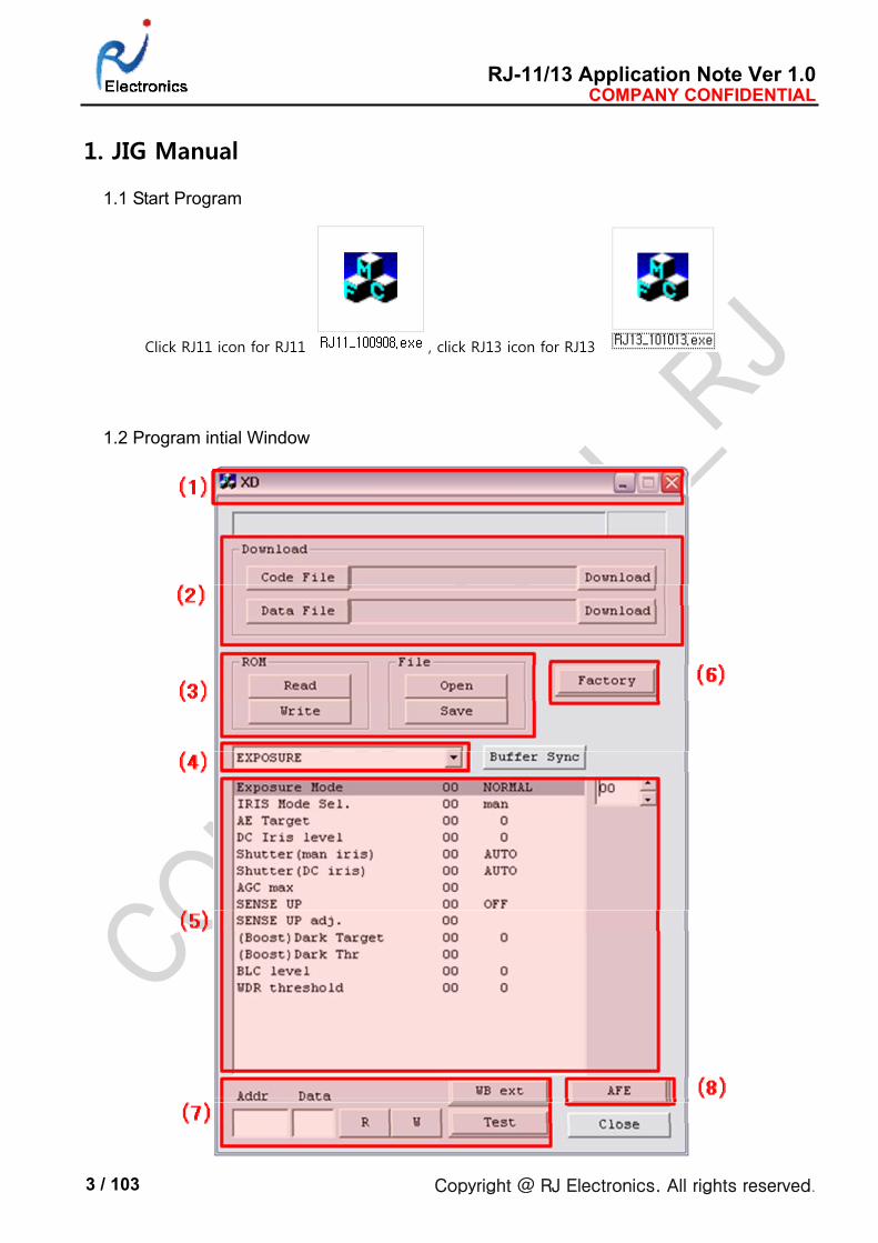
1. JIG Manual
1.1 Start Program
Click RJ11 icon for RJ11 , click RJ13 icon for RJ13
1.2 Program intial Window
RJ-11/13 Application Note Ver 1.0 COMPANY CONFIDENTIAL
Copyright @ RJ Electronics. All rights reserved. 4 / 103
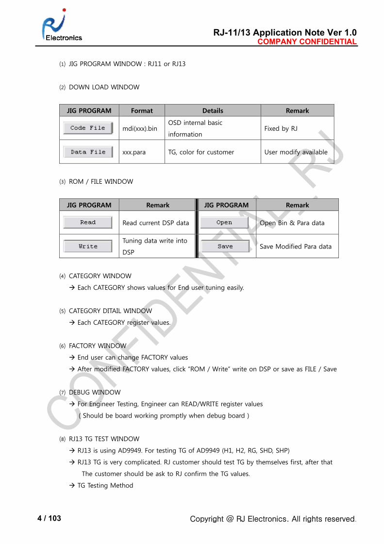
⑴ JIG PROGRAM WINDOW : RJ11 or RJ13
⑵ DOWN LOAD WINDOW
JIG PROGRAM Format Details Remark
mdi(xxx).bin
OSD internal basic
information Fixed by RJ
xxx.para TG, color for customer User modify available
⑶ ROM / FILE WINDOW
JIG PROGRAM Remark JIG PROGRAM Remark
Read current DSP data Open Bin & Para data
Tuning data write into
DSP Save Modified Para data
⑷ CATEGORY WINDOW
Each CATEGORY shows values for End user tuning easily.
⑸ CATEGORY DITAIL WINDOW
Each CATEGORY register values.
⑹ FACTORY WINDOW
End user can change FACTORY values
After modified FACTORY values, click “ROM / Write” write on DSP or save as FILE / Save
⑺ DEBUG WINDOW
For Engineer Testing, Engineer can READ/WRITE register values
( Should be board working promptly when debug board )
⑻ RJ13 TG TEST WINDOW
RJ13 is using AD9949. For testing TG of AD9949 (H1, H2, RG, SHD, SHP)
RJ13 TG is very complicated. RJ customer should test TG by themselves first, after that
The customer should be ask to RJ confirm the TG values.
TG Testing Method
RJ-11/13 Application Note Ver 1.0 COMPANY CONFIDENTIAL
Copyright @ RJ Electronics. All rights reserved. 5 / 103
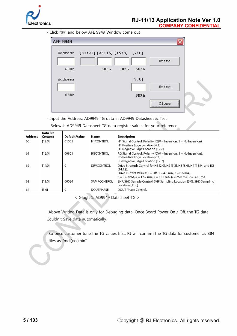
- Click “⑻” and below AFE 9949 Window come out
- Input the Address, AD9949 TG data in AD9949 Datasheet & Test
Below is AD9949 Datasheet TG data register values for your reference
< Gragh 1. AD9949 Datasheet TG >
Above Writing Data is only for Debuging data. Once Board Power On / Off, the TG data
Couldn’t Save data automatically.
So once customer tune the TG values first, RJ will confirm the TG data for customer as BIN
files as “mdi(xxx).bin”
RJ-11/13 Application Note Ver 1.0 COMPANY CONFIDENTIAL
Copyright @ RJ Electronics. All rights reserved. 6 / 103
1.3 Explain CATEGORY WINDOW
1. EXPOSURE
NAME RANGE DESCRIPTION
Exposure Mode 0 ~ 3 0 : Manual Mode 1 : BLC Mode
2 : WDR Mode 3 : HLI Mode
IRIS Mode Sel. 0 ~ 1 0 : Manual Lens 1 : DC Lens
AE Target
DC Iris level 0 ~ 99 Tune current Brigtness
Shutter (man iris)
Shutter (DC iris) 0 ~ 10
0 : AUTO 1 : 1/50 (1/60) 2 : 1/100 3 : 1/120
4 : 1/250 5 : 1/500 6 : 1/1000 7 : 1/2000
8 : 1/4000 9 : 1/10000 10 : 1/100000
AGC max 0 ~ 3 0 : AGC OFF 1 : Low 2 : Middle 3 : High
SENSE UP 0 ~ 8 0 : OFF 1 : X2 2 : X4 3 : X8 4 : X16
5 : X32 6 : X64 7 : X128 8 : X256
SENSE UP adj. -
Starting point of SENSE UP
(Example : 0x10 => at 10dB SENSE UP start
RJ used Ref. 18h now )
(Boost) Dark Target -
Dark condition AE Target.
Dark condition AE Target value
= AE Target value – Dark Target
(Example : AE Target is 40. Dart Target is 30.
Then 40 -30 = 10 Dark condition AE Target )
(Boost) Dark Thr - Starting AGC point
(Example : 0x10 After 10dB AGC start )
BLC level 0h ~ 3h 0h : BLC OFF 1h : Weight Low
2h : Weight Middle 3h : Weight High
WDR
threshold
RJ11 0h ~ 14h WDR starting point ( Ref. Ah)
RJ13 0h ~ Ah WDR Weight ( Ref. 0h)
2. AWB
NAME RANGE DESCRIPTION
AWB mode 0 ~ 3 0 : ATW 1 : AWC
2 : MANUAL 3 : PUSH
Manual R/B gain 0 ~ 255 MANUAL mode R/B control
Lock Awb R/B READ Read current R/B values “READ Register”
G/R/B Pre Gain 0 ~ 255 PRE Gain of G/R/B
AWB R/G/B Min./Max. 0 ~ 255
RJ-11/13 Application Note Ver 1.0 COMPANY CONFIDENTIAL
Copyright @ RJ Electronics. All rights reserved. 7 / 103
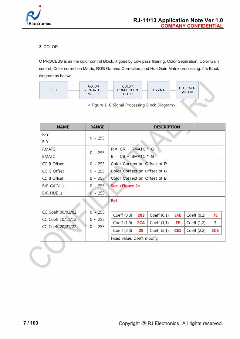
3. COLOR
C PROCESS is as the color control Block, it goes by Low pass filtering, Color Separation, Color Gain
control, Color correction Matrix, RGB Gamma Correction, and Hue Gain Matrix processing. It’s Block
diagram as below.
< Figure 1. C Signal Processing Block Diagram>
NAME RANGE DESCRIPTION
R-Y
B-Y 0 ~ 255
RMATC
BMATC 0 ~ 255
R = CR + RMATC * G
B = CB + BMATC * G
CC R Offset
CC G Offset
CC B Offset
0 ~ 255
0 ~ 255
0 ~ 255
Color Correction Offset of R
Color Correction Offset of G
Color Correction Offset of B
B/R GAIN ±
B/R HUE ±
0 ~ 255
0 ~ 255
See <Figure 2>
CC Coeff 00/01/02
CC Coeff 10/11/12
CC Coeff 20/21/22
0 ~ 255
0 ~ 255
0 ~ 255
Ref
Coeff (0,0) 203 Coeff (0,1) E4E Coeff (0,2) 7E
Coeff (1,0) FCA Coeff (1,1) FE Coeff (1,2) 7
Coeff (2,0) 29 Coeff (2,1) CE1 Coeff (2,2) 3C5
Fixed value. Don’t modify.
RJ-11/13 Application Note Ver 1.0 COMPANY CONFIDENTIAL
Copyright @ RJ Electronics. All rights reserved. 8 / 103
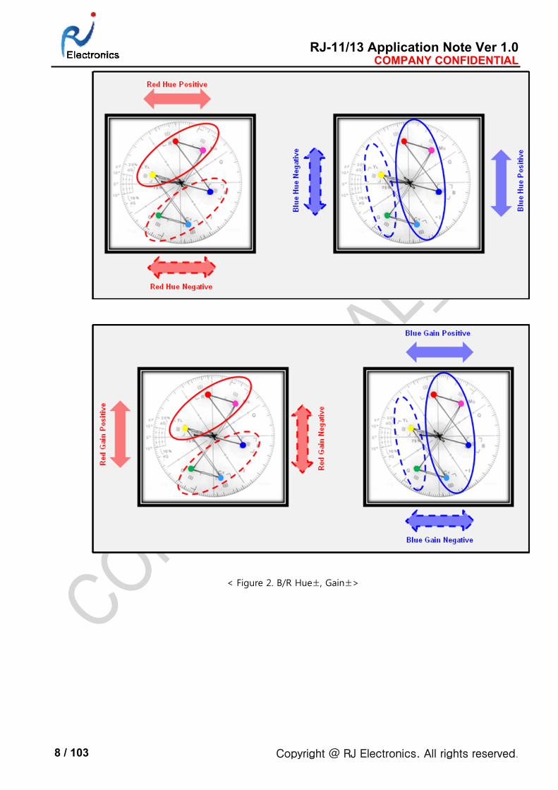
< Figure 2. B/R Hue±, Gain±>
RJ-11/13 Application Note Ver 1.0 COMPANY CONFIDENTIAL
Copyright @ RJ Electronics. All rights reserved. 9 / 103
4. DAY&NIGHT
NAME RANGE DESCRIPTION
Day&Night mode 0 0 : AUTO 1 : DAY 2 : NIGHT 3 : CDS
Day > Night (Auto_Agc)
Night > Day (Auto_Agc) 0 ~ 255
AUTO mode DAY ↔ NIGHT changing point
( Day > Night values should be bigger than
Night > Day values )
Use Burst at Night 0 ~ 1 0 : Burst OFF 1 : Burst ON
( When it’s Night mode, decide to use Burst or not.
Dwell time 0 ~ 10 sec DAY ↔ NIGHT mode change delay time
Day > Night (Reserved)
Night > Day (Reserved) 0 ~ 255 When CDS mode, DAY ↔ NIGHT changing time
Color Sup. Start [dB]
Color Sup. End [dB]
Color Sup. [0~100]
See < Figure 3 >
Sharpness 0 ~ 49
Aperture Sup. Start
Aperture Sup. End
Aperture Sup. [0~100]
See < Figure 3 >
dNR mode 0 ~ 5 0 : 3DNR OFF 1 ~5 : 3DNR Level
Color Sup. (dNR on)
Aper Sup. (dNR on) When 3DNR, Color Sup. / Aper Sup. Values
5. MOTION DETECTION
NAME RANGE DESCRIPTION
Motion Detect 0 ~ 1 0 : Motion OFF 1 : Motion ON
Sensitivity 0 ~ 120 Motion Defecting sensitivity
Alarm mode 0 ~ 2 0 : OFF 1 : Message (show Icon) 2 : AREA
Output time 0 ~ 10 sec When Motion Detection, Alarm output time
Motion Mask 1~4 1 ~ 4 Set up Motion Mask 4 area
Mask 1~4 Start X
Mask 1~4 Start Y
Mask 1~4 End X
Mask 1~4 End Y
X : 0~16
Y : 0~14 Set up each Motion Mask Area
RJ-11/13 Application Note Ver 1.0 COMPANY CONFIDENTIAL
Copyright @ RJ Electronics. All rights reserved. 10 / 103
6. SETUP/SYSTEM
NAME RANGE DESCRIPTION
Ext. Sync mode 0 ~ 1 0 : Internal Mode 1 : Auto Mode
( When Line Lock Mode )
Ext. Sync phase 0 ~ 255
OSD background 0 ~ 1
0 : OSD Background OFF
1 : OSD Background ON
( OSD Background setting )
Language 0 ~ 1 0 : English 1 : Chinese
NTSC mode 0 ~ 1 0 : OFF (PAL Mode) 1 : ON (NTSC Mode)
High Res mode 0 ~ 1 0 : OFF (Normal Mode) 1 : ON (High Mode)
Show TITLE 0 ~ 1 0 : OFF 1 : ON
Title Position X/Y 0 ~ 10/15
Title 01~15 Title (16 character available)
Gamma select 0 ~ 3 0: 0.3 curve 1: 0.45 curve 2: 0.6 curve 3: 1.0 curve
ID number 0 ~ 255
Uart Baud 0 ~ 5 0 : 2400 1 : 4800 2 : 9600 3 : 14400
4 : 19200 5 : 38400
Mirror / Flip 0 ~ 3 0 : OFF 1 : Horizontal 2 : Vertical 3 : Rotation
DPC method 0 ~ 1 0 : DPC OFF 1 : DPC AUTO
D. Zoom mode 0 ~ 1 0 : D. Zoom OFF 1 : D. Zoom ON
D. Zoom level 0 ~ 44
D. Zoom PAN/TILT
DIS mode 0 ~ 1 0 : DIS OFF 1 : DIS ON
Version 01~07
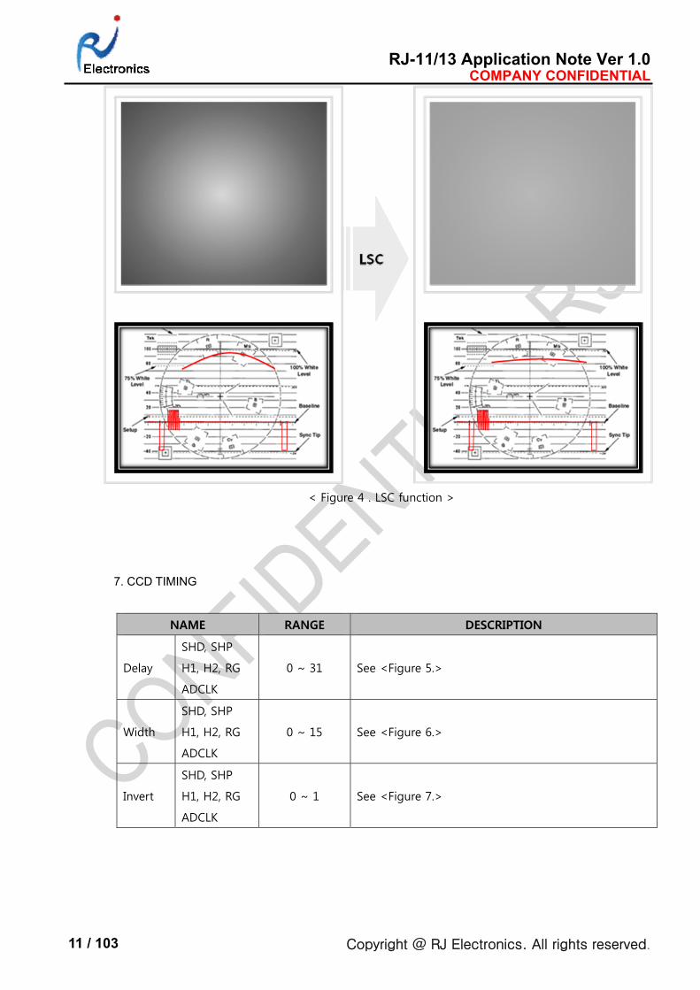
LSC Gain 0 ~ 50 See < Figure 4 >
Lens Center X/Y
RJ-11/13 Application Note Ver 1.0 COMPANY CONFIDENTIAL
Copyright @ RJ Electronics. All rights reserved. 11 / 103
< Figure 4 . LSC function >
7. CCD TIMING
NAME RANGE DESCRIPTION
Delay
SHD, SHP
H1, H2, RG
ADCLK
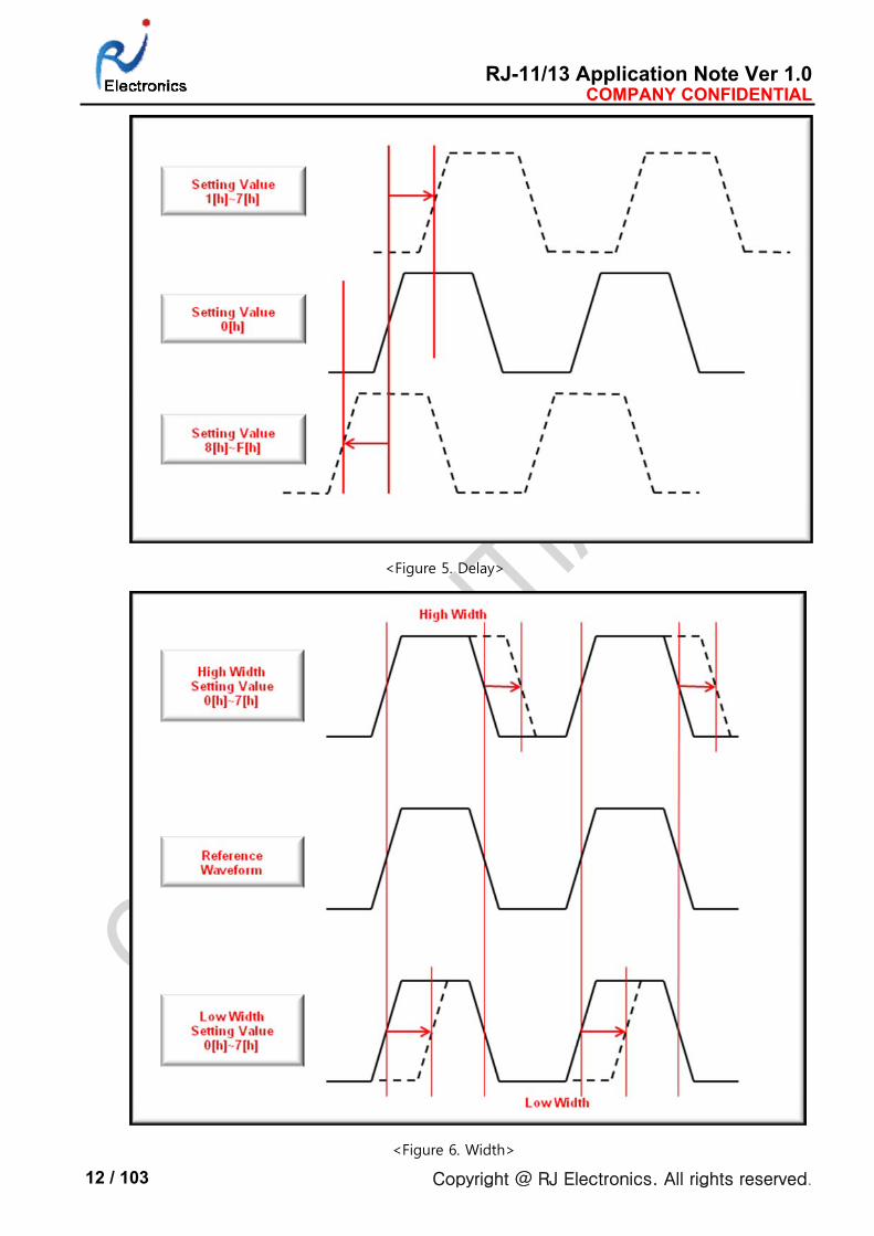
0 ~ 31 See <Figure 5.>
Width
SHD, SHP
H1, H2, RG
ADCLK
0 ~ 15 See <Figure 6.>
Invert
SHD, SHP
H1, H2, RG
ADCLK
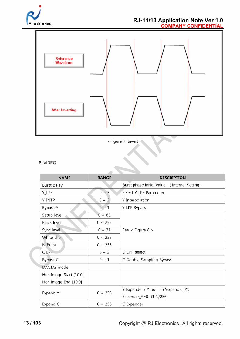
0 ~ 1 See <Figure 7.>
RJ-11/13 Application Note Ver 1.0 COMPANY CONFIDENTIAL
Copyright @ RJ Electronics. All rights reserved. 12 / 103
<Figure 5. Delay>
<Figure 6. Width>
RJ-11/13 Application Note Ver 1.0 COMPANY CONFIDENTIAL
Copyright @ RJ Electronics. All rights reserved. 13 / 103
<Figure 7. Invert>
8. VIDEO
NAME RANGE DESCRIPTION
Burst delay Burst phase Initial Value ( Internal Setting )
Y_LPF 0 ~ 3 Select Y LPF Parameter
Y_INTP 0 ~ 3 Y Interpolation
Bypass Y 0 ~ 1 Y LPF Bypass
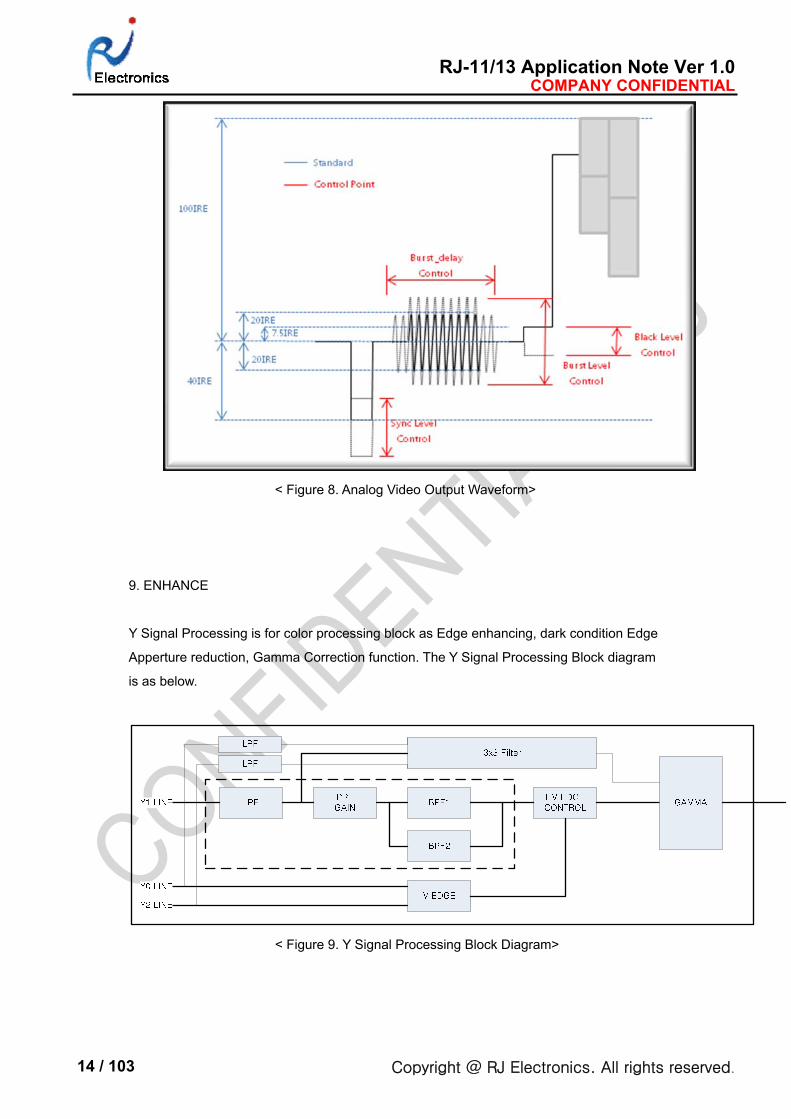
Setup level 0 ~ 63
See < Figure 8 >
Black level 0 ~ 255
Sync level 0 ~ 31
White clip 0 ~ 255
N Burst 0 ~ 255
C LPF 0 ~ 3 C LPF select
Bypass C 0 ~ 1 C Double Sampling Bypass
DAC1/2 mode
Hor. Image Start [10:0]
Hor. Image End [10:0]
Expand Y 0 ~ 255 Y Expander ( Y out = Y*expander_Y),
Expander_Y=0~(1-1/256)
Expand C 0 ~ 255 C Expander
RJ-11/13 Application Note Ver 1.0 COMPANY CONFIDENTIAL
Copyright @ RJ Electronics. All rights reserved. 14 / 103
< Figure 8. Analog Video Output Waveform>
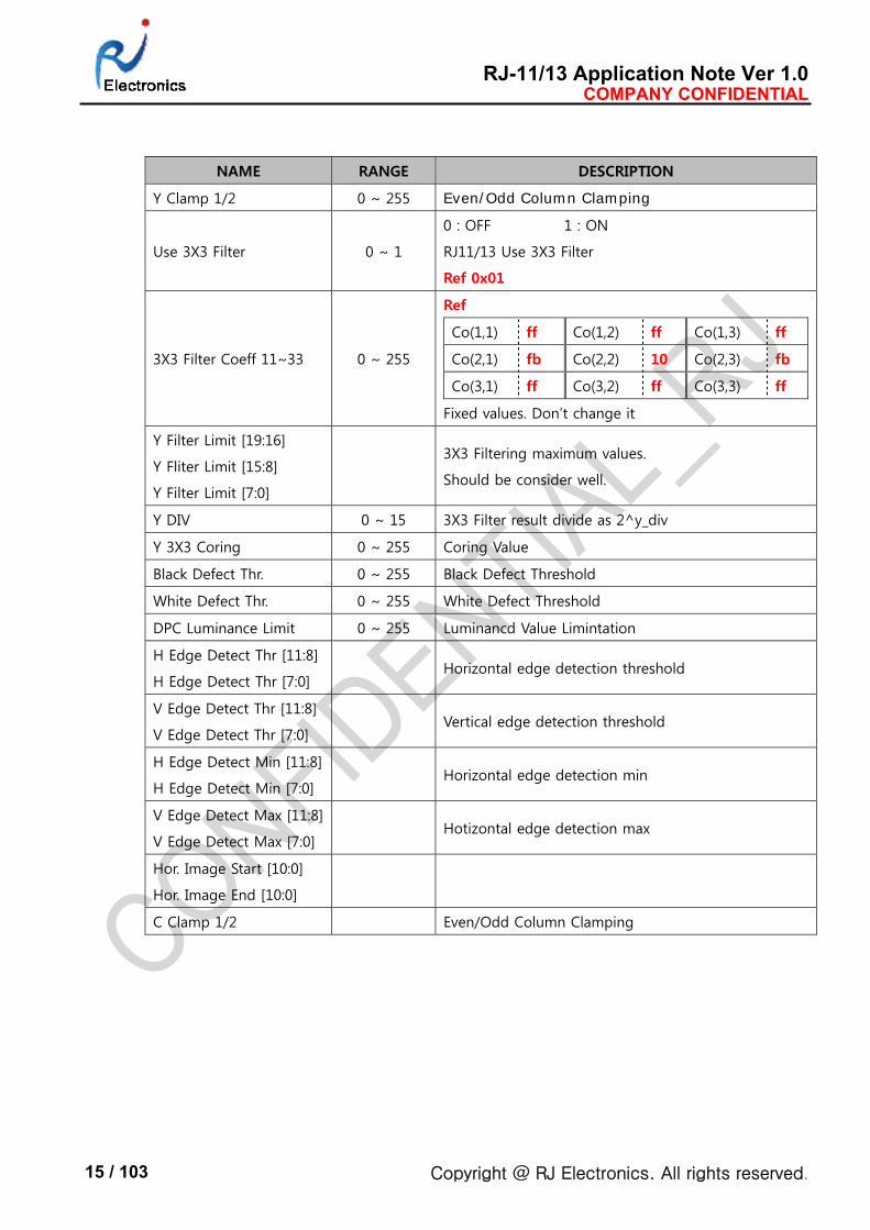
9. ENHANCE
Y Signal Processing is for color processing block as Edge enhancing, dark condition Edge
Apperture reduction, Gamma Correction function. The Y Signal Processing Block diagram
is as below.
< Figure 9. Y Signal Processing Block Diagram>
RJ-11/13 Application Note Ver 1.0 COMPANY CONFIDENTIAL
Copyright @ RJ Electronics. All rights reserved. 15 / 103
NAME RANGE DESCRIPTION
Y Clamp 1/2 0 ~ 255 Even/Odd Column Clamping
Use 3X3 Filter 0 ~ 1
0 : OFF 1 : ON
RJ11/13 Use 3X3 Filter
Ref 0x01
3X3 Filter Coeff 11~33 0 ~ 255
Ref
Co(1,1) ff Co(1,2) ff Co(1,3) ff
Co(2,1) fb Co(2,2) 10 Co(2,3) fb
Co(3,1) ff Co(3,2) ff Co(3,3) ff
Fixed values. Don’t change it
Y Filter Limit [19:16]
Y Fliter Limit [15:8]
Y Filter Limit [7:0]
3X3 Filtering maximum values.
Should be consider well.
Y DIV 0 ~ 15 3X3 Filter result divide as 2^y_div
Y 3X3 Coring 0 ~ 255 Coring Value
Black Defect Thr. 0 ~ 255 Black Defect Threshold
White Defect Thr. 0 ~ 255 White Defect Threshold
DPC Luminance Limit 0 ~ 255 Luminancd Value Limintation
H Edge Detect Thr [11:8]
H Edge Detect Thr [7:0] Horizontal edge detection threshold
V Edge Detect Thr [11:8]
V Edge Detect Thr [7:0] Vertical edge detection threshold
H Edge Detect Min [11:8]
H Edge Detect Min [7:0] Horizontal edge detection min
V Edge Detect Max [11:8]
V Edge Detect Max [7:0] Hotizontal edge detection max
Hor. Image Start [10:0]
Hor. Image End [10:0]
C Clamp 1/2 Even/Odd Column Clamping
RJ-11/13 Application Note Ver 1.0 COMPANY CONFIDENTIAL
Copyright @ RJ Electronics. All rights reserved. 16 / 103
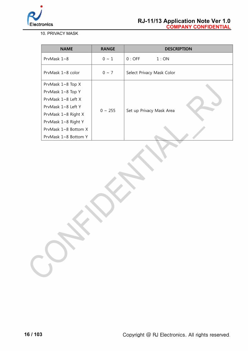
10. PRIVACY MASK
NAME RANGE DESCRIPTION
PrvMask 1~8 0 ~ 1 0 : OFF 1 : ON
PrvMask 1~8 color 0 ~ 7 Select Privacy Mask Color
PrvMask 1~8 Top X
PrvMask 1~8 Top Y
PrvMask 1~8 Left X
PrvMask 1~8 Left Y
PrvMask 1~8 Right X
PrvMask 1~8 Right Y
PrvMask 1~8 Bottom X
PrvMask 1~8 Bottom Y
0 ~ 255 Set up Privacy Mask Area
RJ-11/13 Application Note Ver 1.0 COMPANY CONFIDENTIAL
Copyright @ RJ Electronics. All rights reserved. 17 / 103
RJ-11/13_Y Signal APPLICATION NOTE Ver 1.0
RJ-11/13
Document #: RJ11/13-A01

RJ-11/13 Application Note Ver 1.0 COMPANY CONFIDENTIAL
Copyright @ RJ Electronics. All rights reserved. 18 / 103
REVISION HISTORY
VERSION : Ver 1.0
DATE ;
Author ;
APPROVER ;
Description
ORIGINAL

RJ-11/13 Application Note Ver 1.0 COMPANY CONFIDENTIAL
Copyright @ RJ Electronics. All rights reserved. 19 / 103
This document contains information on a new product. Specifications and information herein are subject to
change without notice.
Use of this specification for product design requires an executed license agreement from RJ Electronics.
RJ Electronics shall not be liable for technical or editorial errors or omissions contained herein; nor for incidental
or consequential damages resulting from the furnishing, performance, or use of this material. Copyright law
protects all parts of the RJ Specification and all rights are reserved. This documentation may not, in whole or in
part, be copied, photocopied, reproduced, translated, or reduced to any electronic medium or machine readable
form without prior consent, in writing, from RJ Electronics.
RJ-11/13 Application Note Ver 1.0 COMPANY CONFIDENTIAL
Copyright @ RJ Electronics. All rights reserved. 20 / 103
TABLE OF CONTENTS
INDEX
REVISION HISTORY .......................................................................................................................................................... 18
TABLE OF CONTENTS ...................................................................................................................................................... 20
1. Y Signal Processing ...................................................................................................................................................... 21
1.1 Y Signal Processing Flow ....................................................................................................................................... 21
1.2 Y Signal Level Control ............................................................................................................................................ 21
● Y Gain ( Y Expander ) ......................................................................................................................................... 21
● Y Offset ( Setup Level ) ...................................................................................................................................... 22
● Y Clip ( White Clip) ............................................................................................................................................. 23
1.3 Y Signal Main Control ............................................................................................................................................. 24
● Y LPF ................................................................................................................................................................... 24
● Y Signal Edge Enhancing .................................................................................................................................. 24
RJ-11/13 Application Note Ver 1.0 COMPANY CONFIDENTIAL
Copyright @ RJ Electronics. All rights reserved. 21 / 103
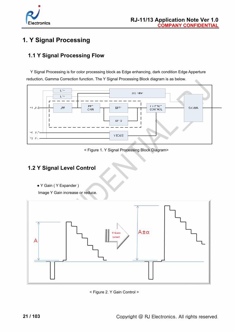
1. Y Signal Processing
1.1 Y Signal Processing Flow
Y Signal Processing is for color processing block as Edge enhancing, dark condition Edge Apperture
reduction, Gamma Correction function. The Y Signal Processing Block diagram is as below.
< Figure 1. Y Signal Processing Block Diagram>
1.2 Y Signal Level Control
● Y Gain ( Y Expander )
Image Y Gain increase or reduce.
< Figure 2. Y Gain Control >
RJ-11/13 Application Note Ver 1.0 COMPANY CONFIDENTIAL
Copyright @ RJ Electronics. All rights reserved. 22 / 103
ADDR BITS NAME RESET MODE DESCRIPTION
Y Gain Control
0x6914 7:0 Expander_y 0 RW Y expander ( yout = y * expander_y),
Expander_y = 0 ~ (1-1/256)
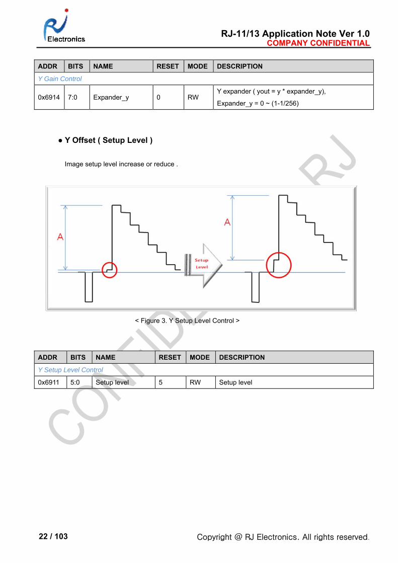
● Y Offset ( Setup Level )
Image setup level increase or reduce .
< Figure 3. Y Setup Level Control >
ADDR BITS NAME RESET MODE DESCRIPTION
Y Setup Level Control
0x6911 5:0 Setup level 5 RW Setup level
RJ-11/13 Application Note Ver 1.0 COMPANY CONFIDENTIAL
Copyright @ RJ Electronics. All rights reserved. 23 / 103
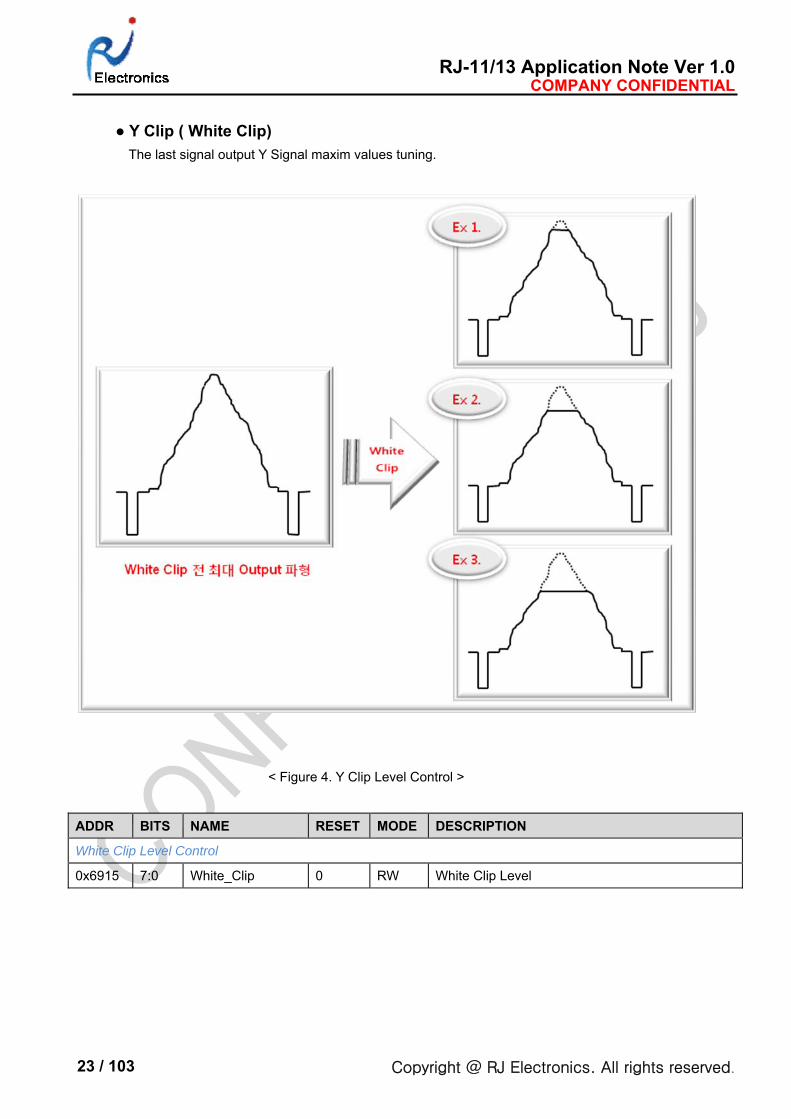
● Y Clip ( White Clip)
The last signal output Y Signal maxim values tuning.
< Figure 4. Y Clip Level Control >
ADDR BITS NAME RESET MODE DESCRIPTION
White Clip Level Control
0x6915 7:0 White_Clip 0 RW White Clip Level
RJ-11/13 Application Note Ver 1.0 COMPANY CONFIDENTIAL
Copyright @ RJ Electronics. All rights reserved. 24 / 103
1.3 Y Signal Main Control
● Y LPF
Y Low Pass Filter is using for reduction of Noise.
ADDR BITS NAME RESET MODE DESCRIPTION
Y LPF Control
0x6908
4:3 Y LPF 2’b11 RW Y LPF parameter selection
2:1 Y_INTP 2’b11 RW Y Interpolation
0 Bypass_y 1’b1 RW Y LPF bypass
● Y Signal Edge Enhancing
RJ-11/13 is designed to get more clear image throught Edge Enhancing processing.
Edge Enhancing is two kind of filter. User can select each method.
Please follow below Register method for your choosing.
ADDR BITS NAME RESET MODE DESCRIPTION
Using Edge Enhancing Filter
0x4020 [0] 3X3FILTER_ENABLE 1 R/W
3x3 filter enable
1: enable
(0x4002 ~ 0x4014 register useless )
0 : disable
(0x4002 ~ 0x4014 register using )
- Using BPF
ADDR BITS NAME RESET MODE DESCRIPTION
Using BPF
0x4002 [5:0] HE_PGAIN 0x00 R/W H_EDGE INPUT GAIN
0x4003 [3:2] BPF1_GAIN 0x0 R/W BPF1 OUTPUT GAIN SELECT
[1:0] HC_GAIN 0x0 R/W H EDGE CORING GAIN SELECT
0x4004 [5:0] HC_LEVEL 0x00 R/W H EDGE CORING LEVEL
0x4005 [3:0] VC_LEVEL 0x00 R/W V EDGE CORING LEVEL
0x4006 [3:0] VC_GAIN 0x00 R/W V EDGE CORING GAIN
0x4007 [3:0] HV_GAIN 0x00 R/W HV EDGE TOTAL GAIN
RJ-11/13 Application Note Ver 1.0 COMPANY CONFIDENTIAL
Copyright @ RJ Electronics. All rights reserved. 25 / 103
0x4008 [3:0] HVC_CORE 0x00 R/W HV CORE LEVEL
0x4009 [0] DB_SEL 0x00 R/W HV DETAIL PART ENHANCER
0x400b [5:0] BPF1_CORE 0x00 R/W BPF1 coring value
0x4010 [5:0] BPF1_GAIN 0x20 R/W BPF1 gain (range : 0/16 ~ 63/16)
EX.) 0X20 = 32/16
- Using 3X3 Filter
ADDR BITS NAME RESET MODE DESCRIPTION
Using 3X3 Filter
0x4021 [7:0] 3X3FILTER_COEFF_11 0xff R/W 3x3filter coefficient (1,1)
Signed , default= -1
0x4022 [7:0] 3X3FILTER_COEFF_12 0xff R/W 3x3filter coefficient (1,2)
Signed , default= -1
0x4023 [7:0] 3X3FILTER_COEFF_13 0xff R/W 3x3filter coefficient (1,3)
Signed , default= -1
0x4024 [7:0] 3X3FILTER_COEFF_21 0xfb R/W 3x3filter coefficient (2,1)
Signed , default= -5
0x4025 [7:0] 3X3FILTER_COEFF_22 0x10 R/W 3x3filter coefficient (2,2)
Signed , default= +16
0x4026 [7:0] 3X3FILTER_COEFF_23 0xfb R/W 3x3filter coefficient (2,3)
Signed , default= -5
0x4027 [7:0] 3X3FILTER_COEFF_31 0xff R/W 3x3filter coefficient (3,1)
Signed , default= -1
0x4028 [7:0] 3X3FILTER_COEFF_32 0xff R/W 3x3filter coefficient (3,2)
Signed , default= -1
0x4029 [7:0] 3X3FILTER_COEFF_33 0xff R/W 3x3filter coefficient (3,3)
Signed , default= -1
0x402d [3:0] Y_DIV 0x2 R/W 3x3filter result divided as 2^y_div
0x402e [7:0] Y3X3_GAIN 0x10 R/W Gain ( x1/16 )
Default = 1.0
0x402f [7:0] Y3X3_CORING 0x0e R/W Coring Value
RJ-11/13 Application Note Ver 1.0 COMPANY CONFIDENTIAL
Copyright @ RJ Electronics. All rights reserved. 26 / 103
RJ-11/13_C Signal APPLICATION NOTE Ver 1.0
RJ-11/13
Document #: RJ11/13-A01

RJ-11/13 Application Note Ver 1.0 COMPANY CONFIDENTIAL
Copyright @ RJ Electronics. All rights reserved. 27 / 103
REVISION HISTORY
VERSION : Ver 1.0
DATE ;
Author ;
APPROVER ;
Description
ORIGINAL

RJ-11/13 Application Note Ver 1.0 COMPANY CONFIDENTIAL
Copyright @ RJ Electronics. All rights reserved. 28 / 103
This document contains information on a new product. Specifications and information herein are subject to
change without notice.
Use of this specification for product design requires an executed license agreement from HT RJ Electronics.
RJ Electronics shall not be liable for technical or editorial errors or omissions contained herein; nor for incidental
or consequential damages resulting from the furnishing, performance, or use of this material. Copyright law
protects all parts of the RJ Specification and all rights are reserved. This documentation may not, in whole or in
part, be copied, photocopied, reproduced, translated, or reduced to any electronic medium or machine readable
form without prior consent, in writing, from RJ Electronics.
RJ-11/13 Application Note Ver 1.0 COMPANY CONFIDENTIAL
Copyright @ RJ Electronics. All rights reserved. 29 / 103
TABLE OF CONTENTS
CONTENTS REVISION HISTORY .......................................................................................................................................................... 27
TABLE OF CONTENTS ...................................................................................................................................................... 29
1. C Signal Processing ...................................................................................................................................................... 30
1.1 C Signal Processing Flow ....................................................................................................................................... 30
1.2 C Signal Main Control ............................................................................................................................................. 30
● C LPF ................................................................................................................................................................... 30
● Color Separation Matrix ..................................................................................................................................... 30
● Color Correction Matrix ..................................................................................................................................... 31
RJ-11/13 Application Note Ver 1.0 COMPANY CONFIDENTIAL
Copyright @ RJ Electronics. All rights reserved. 30 / 103
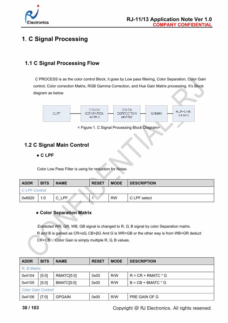
1. C Signal Processing
1.1 C Signal Processing Flow
C PROCESS is as the color control Block, it goes by Low pass filtering, Color Separation, Color Gain
control, Color correction Matrix, RGB Gamma Correction, and Hue Gain Matrix processing. It’s Block
diagram as below.
< Figure 1. C Signal Processing Block Diagram>
1.2 C Signal Main Control
● C LPF
Color Low Pass Filter is using for reduction for Noise.
ADDR BITS NAME RESET MODE DESCRIPTION
C LPF Control
0x6920 1:0 C_LPF 1 RW C LPF select
● Color Separation Matrix
Extracted WR, GR, WB, GB signal is changed to R, G, B signal by color Separation matrix.
R and B is gained as CR+αG, CB+βG. And G is WR+GB or the other way is from WB+GR deduct
CR+CB. Color Gain is simply multiple R, G, B values.
ADDR BITS NAME RESET MODE DESCRIPTION
R, B Matrix
0x4104 [5:0] RMATC[5:0] 0x00 R/W R = CR + RMATC * G
0x4105 [5:0] BMATC[5:0] 0x00 R/W B = CB + BMATC * G
Color Gain Control
0x4106 [7:0] GPGAIN 0x00 R/W PRE GAIN OF G
RJ-11/13 Application Note Ver 1.0 COMPANY CONFIDENTIAL
Copyright @ RJ Electronics. All rights reserved. 31 / 103
0x4107 [7:0] RPGAIN 0x00 R/W PRE GAIN OF R
0x4108 [7:0] BPGAIN 0x00 R/W PRE GAIN OF B
● Color Correction Matrix
Color Correction Matrix make as 3X3 matrix. Matrix Coefficient is ±3.999 .
ADDR BITS NAME RESET MODE DESCRIPTION
Color Correction Matrix
0x4183 [3:0] CC_COEFF00[11:8] 0x0
R/W
Color Correction Coefficient 00 position
(2 number of steps int: [11:8], fraction: 7:0)
color correction coefficient is same position 0x4184 [7:0] CC_COEFF00[7:0] 0x00
0x4185 [3:0] CC_COEFF01[11:8] 0x0 R/W Color Correction Coefficient 01 position
0x4186 [7:0] CC_COEFF01[7:0] 0x00
0x4187 [3:0] CC_COEFF02[11:8] 0x0 R/W Color Correction Coefficient 02 position
0x4188 [7:0] CC_COEFF02[7:0] 0x00
0x4189 [3:0] CC_COEFF10[11:8] 0x0 R/W Color Correction Coefficient 10 position
0x418A [7:0] CC_COEFF10[7:0] 0x00
0x418B [3:0] CC_COEFF11[11:8] 0x0 R/W Color Correction Coefficient 11 position
0x418C [7:0] CC_COEFF11[7:0] 0x00
0x418D [3:0] CC_COEFF12[11:8] 0x0 R/W Color Correction Coefficient 12 position
0x418E [7:0] CC_COEFF12[7:0] 0x00
0x418F [3:0] CC_COEFF20[11:8] 0x0 R/W Color Correction Coefficient 20 position
0x4190 [7:0] CC_COEFF20[7:0] 0x00
0x4191 [3:0] CC_COEFF21[11:8] 0x0 R/W Color Correction Coefficient 21 position
0x4192 [7:0] CC_COEFF21[7:0] 0x00
0x4193 [3:0] CC_COEFF22[11:8] 0x0 R/W Color Correction Coefficient 22 position
0x4194 [7:0] CC_COEFF22[7:0] 0x00
- Color Hue adjustment
RJ-11/13 Application Note Ver 1.0 COMPANY CONFIDENTIAL
Copyright @ RJ Electronics. All rights reserved. 32 / 103
- Color Gain adjustment
ADDR BITS NAME RESET MODE DESCRIPTION
Color Hue / Gain Control
0x410D [7:0] BGAIN_P 0x00 R/W B-G POSITIVE GAIN (2’s Complement)
0x410E [7:0] BGAIN_N 0x00 R/W B-G NEGATIVE GAIN (2’s Complement)
0x410F [7:0] BHUE_P 0x00 R/W B-G HUE (2’s Complement)
0x4110 [7:0] BHUE_N 0x00 R/W B-G HUE (2’s Complement)
0x4111 [7:0] RGAIN_P 0x00 R/W R-G GAIN (2’s Complement)
RJ-11/13 Application Note Ver 1.0 COMPANY CONFIDENTIAL
Copyright @ RJ Electronics. All rights reserved. 33 / 103
0x4112 [7:0] RGAIN_N 0x00 R/W R-G GAIN (2’s Complement)
0x4113 [7:0] RHUE_P 0x00 R/W R-G HUE Positive (2’s complement)
0x4114 [7:0] RHUE_N 0x00 R/W R-G HUE Negative (2’s complement)
RJ-11/13 Application Note Ver 1.0 COMPANY CONFIDENTIAL
Copyright @ RJ Electronics. All rights reserved. 34 / 103
RJ-11/13_TG APPLICATION NOTE Ver 1.0
RJ-11/13
Document #: RJ11/13-A01

RJ-11/13 Application Note Ver 1.0 COMPANY CONFIDENTIAL
Copyright @ RJ Electronics. All rights reserved. 35 / 103
REVISION HISTORY
VERSION : Ver 1.0
DATE ;
Author ;
APPROVER ;
Description
ORIGINAL
RJ-11/13 Application Note Ver 1.0 COMPANY CONFIDENTIAL
Copyright @ RJ Electronics. All rights reserved. 36 / 103
This document contains information on a new product. Specifications and information herein are subject to
change without notice.
Use of this specification for product design requires an executed license agreement from RJ Electronics.
RJ Electronics shall not be liable for technical or editorial errors or omissions contained herein; nor for incidental
or consequential damages resulting from the furnishing, performance, or use of this material. Copyright law
protects all parts of the RJ Electronics Specification and all rights are reserved. This documentation may not, in
whole or in part, be copied, photocopied, reproduced, translated, or reduced to any electronic medium or
machine readable form without prior consent, in writing, from RJ Electronics.
RJ-11/13 Application Note Ver 1.0 COMPANY CONFIDENTIAL
Copyright @ RJ Electronics. All rights reserved. 37 / 103
TABLE OF CONTENTS
INDEX
REVISION HISTORY .......................................................................................................................................................... 35
TABLE OF CONTENTS ...................................................................................................................................................... 37
1. Timing Generator .......................................................................................................................................................... 38
1.1 Delay Adjustment .................................................................................................................................................... 38
1.2 Width Adjustment .................................................................................................................................................... 39
1.3 Inverting Adjustment ............................................................................................................................................... 41
RJ-11/13 Application Note Ver 1.0 COMPANY CONFIDENTIAL
Copyright @ RJ Electronics. All rights reserved. 38 / 103
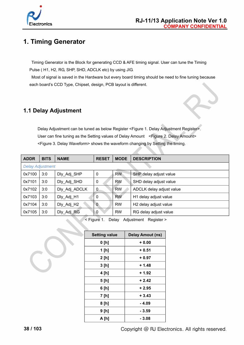
1. Timing Generator
Timing Generator is the Block for generating CCD & AFE timing signal. User can tune the Timing
Pulse ( H1, H2, RG, SHP, SHD, ADCLK etc) by using JIG.
Most of signal is saved in the Hardware but every board timing should be need to fine tuning because
each board’s CCD Type, Chipset, design, PCB layout is different.
1.1 Delay Adjustment
Delay Adjustment can be tuned as below Register <Figure 1. Delay Adjustment Register>.
User can fine tuning as the Setting values of Delay Amount <Figure 2. Delay Amount>
<Figure 3. Delay Waveform> shows the waveform changing by Setting the timing.
ADDR BITS NAME RESET MODE DESCRIPTION
Delay Adjustment
0x7100 3:0 Dly_Adj_SHP 0 RW SHP delay adjust value
0x7101 3:0 Dly_Adj_SHD 0 RW SHD delay adjust value
0x7102 3:0 Dly_Adj_ADCLK 0 RW ADCLK delay adjust value
0x7103 3:0 Dly_Adj_H1 0 RW H1 delay adjust value
0x7104 3:0 Dly_Adj_H2 0 RW H2 delay adjust value
0x7105 3:0 Dly_Adj_RG 0 RW RG delay adjust value
< Figure 1. Delay Adjustment Register >
Setting value Delay Amout (ns)
0 [h] + 0.00
1 [h] + 0.51
2 [h] + 0.97
3 [h] + 1.48
4 [h] + 1.92
5 [h] + 2.42
6 [h] + 2.95
7 [h] + 3.43
8 [h] - 4.09
9 [h] - 3.59
A [h] - 3.08
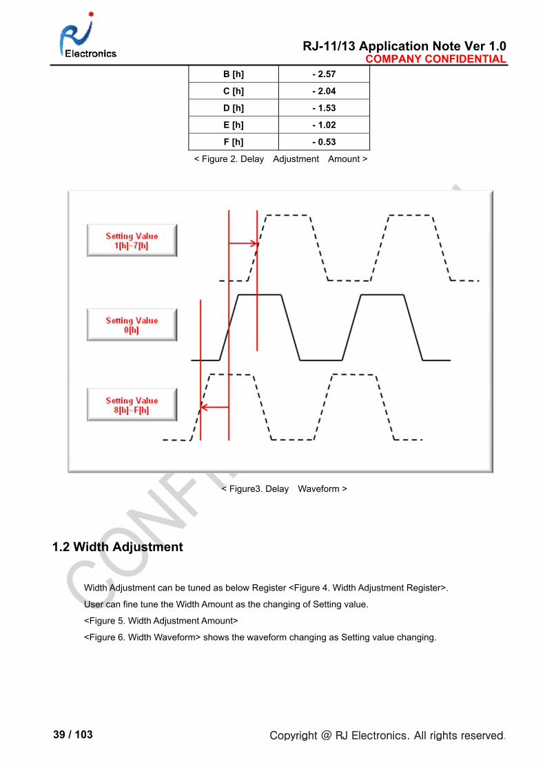
RJ-11/13 Application Note Ver 1.0 COMPANY CONFIDENTIAL
Copyright @ RJ Electronics. All rights reserved. 39 / 103
B [h] - 2.57
C [h] - 2.04
D [h] - 1.53
E [h] - 1.02
F [h] - 0.53
< Figure 2. Delay Adjustment Amount >
< Figure3. Delay Waveform >
1.2 Width Adjustment
Width Adjustment can be tuned as below Register <Figure 4. Width Adjustment Register>.
User can fine tune the Width Amount as the changing of Setting value.
<Figure 5. Width Adjustment Amount>
<Figure 6. Width Waveform> shows the waveform changing as Setting value changing.
RJ-11/13 Application Note Ver 1.0 COMPANY CONFIDENTIAL
Copyright @ RJ Electronics. All rights reserved. 40 / 103
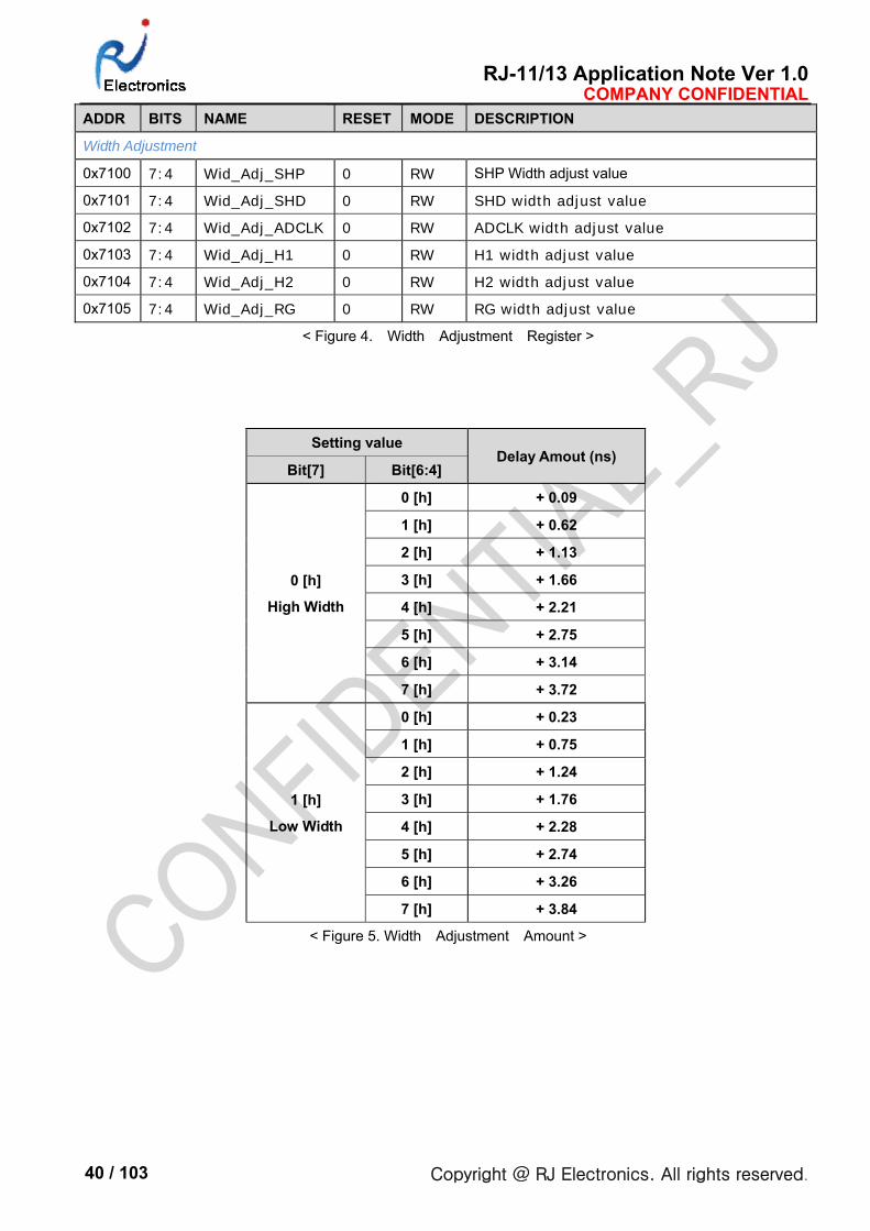
ADDR BITS NAME RESET MODE DESCRIPTION
Width Adjustment
0x7100 7:4 Wid_Adj_SHP 0 RW SHP Width adjust value
0x7101 7:4 Wid_Adj_SHD 0 RW SHD width adjust value
0x7102 7:4 Wid_Adj_ADCLK 0 RW ADCLK width adjust value
0x7103 7:4 Wid_Adj_H1 0 RW H1 width adjust value
0x7104 7:4 Wid_Adj_H2 0 RW H2 width adjust value
0x7105 7:4 Wid_Adj_RG 0 RW RG width adjust value
< Figure 4. Width Adjustment Register >
Setting value Delay Amout (ns)
Bit[7] Bit[6:4]
0 [h]
High Width
0 [h] + 0.09
1 [h] + 0.62
2 [h] + 1.13
3 [h] + 1.66
4 [h] + 2.21
5 [h] + 2.75
6 [h] + 3.14
7 [h] + 3.72
1 [h]
Low Width
0 [h] + 0.23
1 [h] + 0.75
2 [h] + 1.24
3 [h] + 1.76
4 [h] + 2.28
5 [h] + 2.74
6 [h] + 3.26
7 [h] + 3.84
< Figure 5. Width Adjustment Amount >
RJ-11/13 Application Note Ver 1.0 COMPANY CONFIDENTIAL
Copyright @ RJ Electronics. All rights reserved. 41 / 103
< Figure 6. Width Waveform >
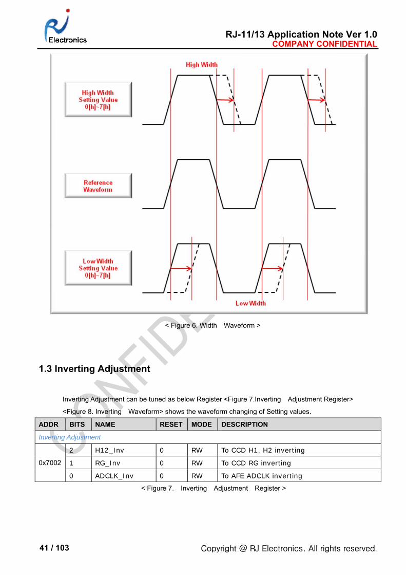
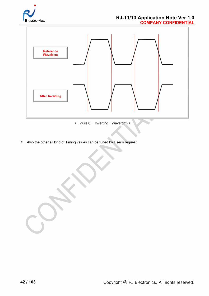
1.3 Inverting Adjustment
Inverting Adjustment can be tuned as below Register <Figure 7.Inverting Adjustment Register>
<Figure 8. Inverting Waveform> shows the waveform changing of Setting values.
ADDR BITS NAME RESET MODE DESCRIPTION
Inverting Adjustment
0x7002
2 H12_Inv 0 RW To CCD H1, H2 inverting
1 RG_Inv 0 RW To CCD RG inverting
0 ADCLK_Inv 0 RW To AFE ADCLK inverting
< Figure 7. Inverting Adjustment Register >
RJ-11/13 Application Note Ver 1.0 COMPANY CONFIDENTIAL
Copyright @ RJ Electronics. All rights reserved. 42 / 103
< Figure 8. Inverting Waveform >
※ Also the other all kind of Timing values can be tuned by User’s request.
RJ-11/13 Application Note Ver 1.0 COMPANY CONFIDENTIAL
Copyright @ RJ Electronics. All rights reserved. 43 / 103
RJ-11/13_Gamma APPLICATION NOTE Ver 1.0
RJ-11/13
Document #: RJ11/13-A01

RJ-11/13 Application Note Ver 1.0 COMPANY CONFIDENTIAL
Copyright @ RJ Electronics. All rights reserved. 44 / 103
REVISION HISTORY
VERSION : Ver 1.0
DATE ;
Author ;
APPROVER ;
Description
ORIGINAL
RJ-11/13 Application Note Ver 1.0 COMPANY CONFIDENTIAL
Copyright @ RJ Electronics. All rights reserved. 45 / 103
This document contains information on a new product. Specifications and information herein are subject to
change without notice.
Use of this specification for product design requires an executed license agreement from RJ Electronics.
RJ Electronics shall not be liable for technical or editorial errors or omissions contained herein; nor for incidental
or consequential damages resulting from the furnishing, performance, or use of this material. Copyright law
protects all parts of the RJ Specification and all rights are reserved. This documentation may not, in whole or in
part, be copied, photocopied, reproduced, translated, or reduced to any electronic medium or machine readable
form without prior consent, in writing, from RJ Electronics.
RJ-11/13 Application Note Ver 1.0 COMPANY CONFIDENTIAL
Copyright @ RJ Electronics. All rights reserved. 46 / 103
TABLE OF CONTENTS
INDEX REVISION HISTORY .......................................................................................................................................................... 44
TABLE OF CONTENTS ...................................................................................................................................................... 46
1. Gamma Processing ....................................................................................................................................................... 47
1.1 Y Gamma ................................................................................................................................................................ 47
1.2 C Gamma ................................................................................................................................................................ 49
RJ-11/13 Application Note Ver 1.0 COMPANY CONFIDENTIAL
Copyright @ RJ Electronics. All rights reserved. 47 / 103
1. Gamma Processing
1.1 Y Gamma
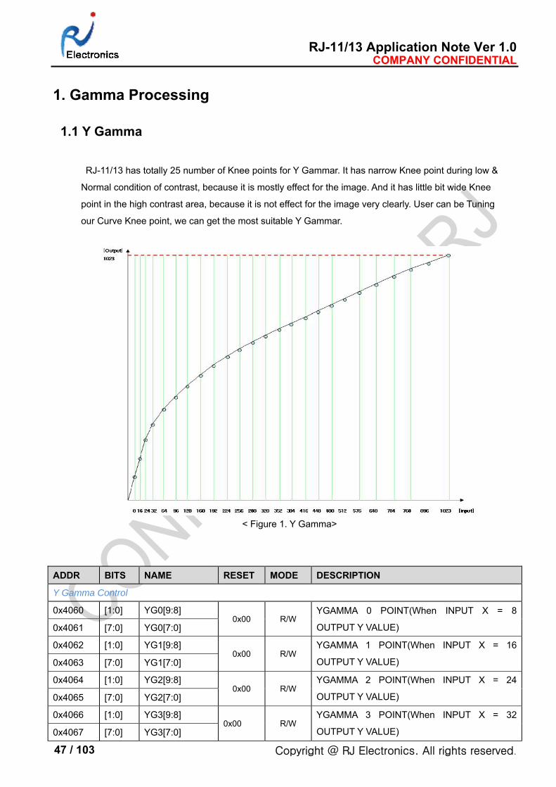
RJ-11/13 has totally 25 number of Knee points for Y Gammar. It has narrow Knee point during low &
Normal condition of contrast, because it is mostly effect for the image. And it has little bit wide Knee
point in the high contrast area, because it is not effect for the image very clearly. User can be Tuning
our Curve Knee point, we can get the most suitable Y Gammar.
< Figure 1. Y Gamma>
ADDR BITS NAME RESET MODE DESCRIPTION
Y Gamma Control
0x4060 [1:0] YG0[9:8] 0x00 R/W
YGAMMA 0 POINT(When INPUT X = 8
OUTPUT Y VALUE) 0x4061 [7:0] YG0[7:0]
0x4062 [1:0] YG1[9:8] 0x00 R/W
YGAMMA 1 POINT(When INPUT X = 16
OUTPUT Y VALUE) 0x4063 [7:0] YG1[7:0]
0x4064 [1:0] YG2[9:8] 0x00 R/W
YGAMMA 2 POINT(When INPUT X = 24
OUTPUT Y VALUE) 0x4065 [7:0] YG2[7:0]
0x4066 [1:0] YG3[9:8] 0x00 R/W
YGAMMA 3 POINT(When INPUT X = 32
OUTPUT Y VALUE) 0x4067 [7:0] YG3[7:0]
RJ-11/13 Application Note Ver 1.0 COMPANY CONFIDENTIAL
Copyright @ RJ Electronics. All rights reserved. 48 / 103
0x4068 [1:0] YG4[9:8] 0x00 R/W
YGAMMA 4 POINT(Whn INPUT X = 64
OUTPUT Y VALUE) 0x4069 [7:0] YG4[7:0]
0x406A [1:0] YG5[9:8] 0x00 R/W
YGAMMA 5 POINT(When INPUT X = 96
OUTPUT Y VALUE) 0x406B [7:0] YG5[7:0]
0x406C [1:0] YG6[9:8] 0x00 R/W
YGAMMA 6 POINT(When INPUT X = 128
OUTPUT Y VALUE) 0x406D [7:0] YG6[7:0]
0x406E [1:0] YG7[9:8] 0x00 R/W
YGAMMA 7 POINT(When INPUT X = 160
OUTPUT Y VALUE) 0x406F [7:0] YG7[7:0]
0x4070 [1:0] YG8[9:8] 0x00 R/W
YGAMMA 8 POINT(When INPUT X = 192
OUTPUT Y VALUE) 0x4071 [7:0] YG8[7:0]
0x4072 [1:0] YG9[9:8] 0x00 R/W
YGAMMA 9 POINT(When INPUT X = 224
OUTPUT Y VALUE) 0x4073 [7:0] YG9[7:0]
0x4074 [1:0] YG10[9:8] 0x00 R/W
YGAMMA 10 POINT(When INPUT X = 256
OUTPUT Y VALUE) 0x4075 [7:0] YG10[7:0]
0x4076 [1:0] YG11[9:8] 0x00 R/W
YGAMMA 11 POINT(When INPUT X = 288
OUTPUT Y VALUE) 0x4077 [7:0] YG11[7:0]
0x4078 [1:0] YG12[9:8] 0x00 R/W
YGAMMA 12 POINT(When INPUT X = 320
OUTPUT Y VALUE) 0x4079 [7:0] YG12[7:0]
0x407A [1:0] YG13[9:8] 0x00 R/W
YGAMMA 13 POINT(When INPUT X = 352
OUTPUT Y VALUE) 0x407B [7:0] YG13[7:0]
0x407C [1:0] YG14[9:8] 0x00 R/W
YGAMMA 14 POINT(When INPUT X = 384
OUTPUT Y VALUE) 0x407D [7:0] YG14[7:0]
0x407E [1:0] YG15[9:8] 0x00 R/W
YGAMMA 15 POINT(When INPUT X = 416
OUTPUT Y VALUE) 0x407F [7:0] YG15[7:0]
0x4080 [1:0] YG16[9:8] 0x00 R/W
YGAMMA 16 POINT(When INPUT X = 448
OUTPUT Y VALUE) 0x4081 [7:0] YG16[7:0]
0x4082 [1:0] YG17[9:8] 0x00 R/W
YGAMMA 17 POINT(When INPUT X = 480
OUTPUT Y VALUE) 0x4083 [7:0] YG17[7:0]
0x4084 [1:0] YG18[9:8] 0x00 R/W
YGAMMA 18 POINT(When INPUT X = 512
OUTPUT Y VALUE) 0x4085 [7:0] YG18[7:0]
0x4086 [1:0] YG19[9:8] 0x00 R/W
YGAMMA 19 POINT(When INPUT X = 576
OUTPUT Y VALUE) 0x4087 [7:0] YG19[7:0]
0x4088 [1:0] YG20[9:8] 0x00 R/W
YGAMMA 20 POINT(When INPUT X = 640
OUTPUT Y VALUE) 0x4089 [7:0] YG20[7:0]
0x408A [1:0] YG21[9:8] 0x00 R/W
YGAMMA 21 POINT(When INPUT X = 704
OUTPUT Y VALUE) 0x408B [7:0] YG21[7:0]
0x408C [1:0] YG22[9:8] 0x00 R/W
YGAMMA 22 POINT(When INPUT X = 768
OUTPUT Y VALUE) 0x408D [7:0] YG22[7:0]
RJ-11/13 Application Note Ver 1.0 COMPANY CONFIDENTIAL
Copyright @ RJ Electronics. All rights reserved. 49 / 103
0x408E [1:0] YG23[9:8] 0x00 R/W
YGAMMA 23 POINT(When INPUT X = 896
OUTPUT Y VALUE) 0x408F [7:0] YG23[7:0]
0x4090 [1:0] YG24[9:8] 0x00 R/W
YGAMMA 24 POINT(When INPUT X = 1023
OUTPUT Y VALUE) 0x4091 [7:0] YG24[7:0]
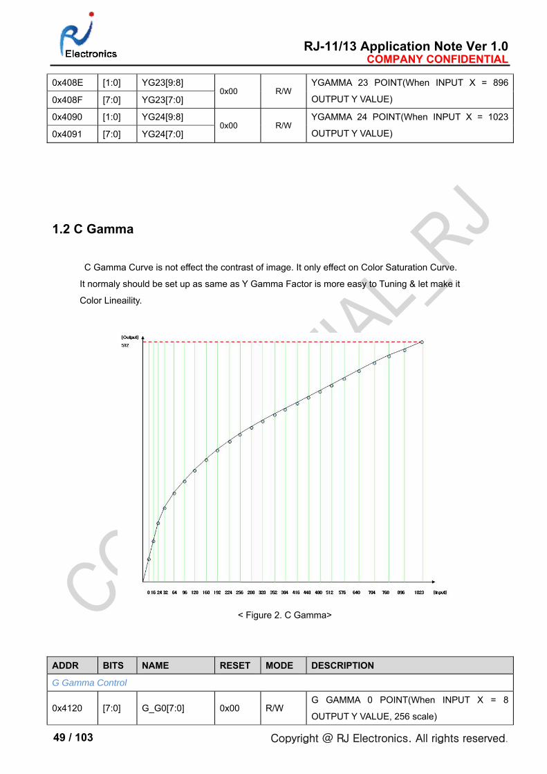
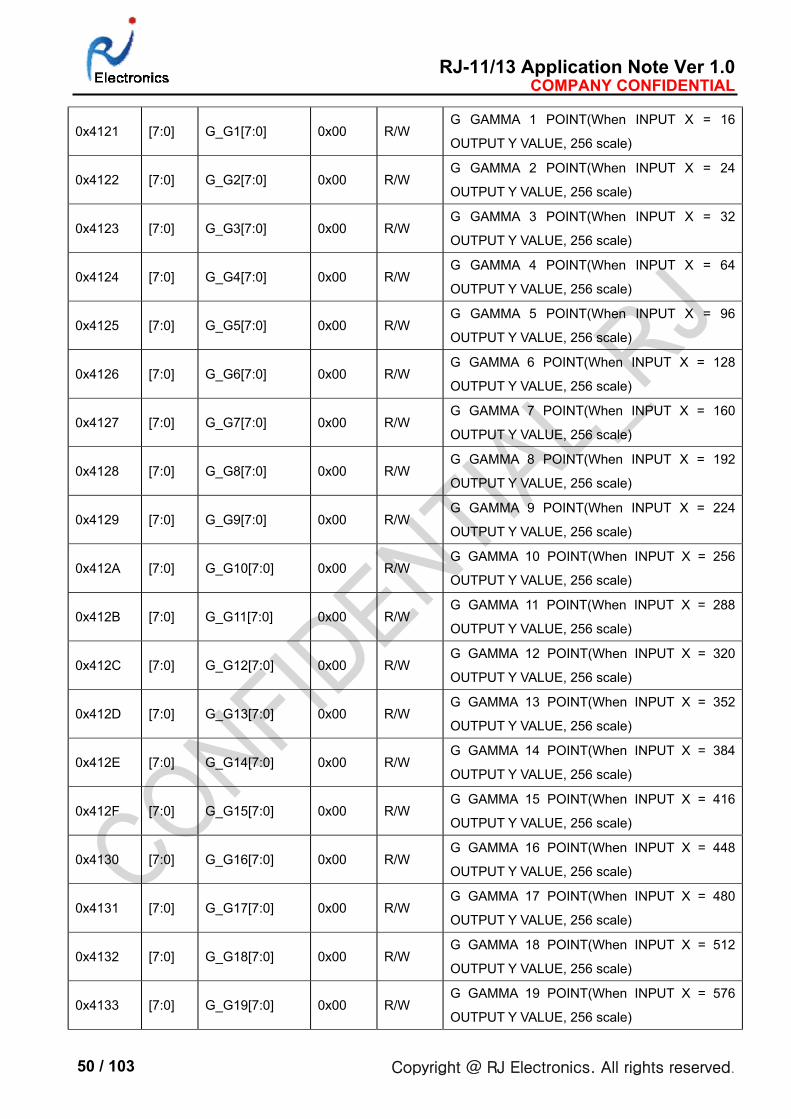
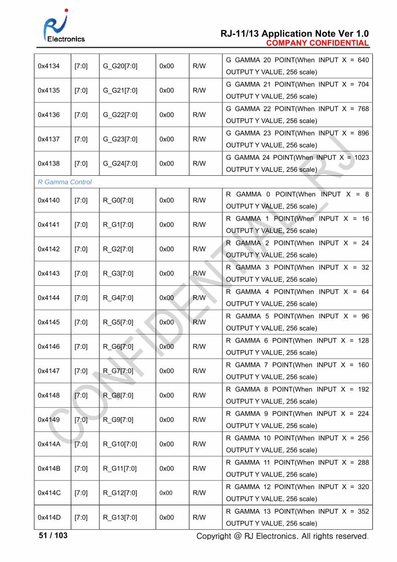
1.2 C Gamma
C Gamma Curve is not effect the contrast of image. It only effect on Color Saturation Curve.
It normaly should be set up as same as Y Gamma Factor is more easy to Tuning & let make it
Color Lineaility.
< Figure 2. C Gamma>
ADDR BITS NAME RESET MODE DESCRIPTION
G Gamma Control
0x4120 [7:0] G_G0[7:0] 0x00 R/W G GAMMA 0 POINT(When INPUT X = 8
OUTPUT Y VALUE, 256 scale)
RJ-11/13 Application Note Ver 1.0 COMPANY CONFIDENTIAL
Copyright @ RJ Electronics. All rights reserved. 50 / 103
0x4121 [7:0] G_G1[7:0] 0x00 R/W G GAMMA 1 POINT(When INPUT X = 16
OUTPUT Y VALUE, 256 scale)
0x4122 [7:0] G_G2[7:0] 0x00 R/W G GAMMA 2 POINT(When INPUT X = 24
OUTPUT Y VALUE, 256 scale)
0x4123 [7:0] G_G3[7:0] 0x00 R/W G GAMMA 3 POINT(When INPUT X = 32
OUTPUT Y VALUE, 256 scale)
0x4124 [7:0] G_G4[7:0] 0x00 R/W G GAMMA 4 POINT(When INPUT X = 64
OUTPUT Y VALUE, 256 scale)
0x4125 [7:0] G_G5[7:0] 0x00 R/W G GAMMA 5 POINT(When INPUT X = 96
OUTPUT Y VALUE, 256 scale)
0x4126 [7:0] G_G6[7:0] 0x00 R/W G GAMMA 6 POINT(When INPUT X = 128
OUTPUT Y VALUE, 256 scale)
0x4127 [7:0] G_G7[7:0] 0x00 R/W G GAMMA 7 POINT(When INPUT X = 160
OUTPUT Y VALUE, 256 scale)
0x4128 [7:0] G_G8[7:0] 0x00 R/W G GAMMA 8 POINT(When INPUT X = 192
OUTPUT Y VALUE, 256 scale)
0x4129 [7:0] G_G9[7:0] 0x00 R/W G GAMMA 9 POINT(When INPUT X = 224
OUTPUT Y VALUE, 256 scale)
0x412A [7:0] G_G10[7:0] 0x00 R/W G GAMMA 10 POINT(When INPUT X = 256
OUTPUT Y VALUE, 256 scale)
0x412B [7:0] G_G11[7:0] 0x00 R/W G GAMMA 11 POINT(When INPUT X = 288
OUTPUT Y VALUE, 256 scale)
0x412C [7:0] G_G12[7:0] 0x00 R/W G GAMMA 12 POINT(When INPUT X = 320
OUTPUT Y VALUE, 256 scale)
0x412D [7:0] G_G13[7:0] 0x00 R/W G GAMMA 13 POINT(When INPUT X = 352
OUTPUT Y VALUE, 256 scale)
0x412E [7:0] G_G14[7:0] 0x00 R/W G GAMMA 14 POINT(When INPUT X = 384
OUTPUT Y VALUE, 256 scale)
0x412F [7:0] G_G15[7:0] 0x00 R/W G GAMMA 15 POINT(When INPUT X = 416
OUTPUT Y VALUE, 256 scale)
0x4130 [7:0] G_G16[7:0] 0x00 R/W G GAMMA 16 POINT(When INPUT X = 448
OUTPUT Y VALUE, 256 scale)
0x4131 [7:0] G_G17[7:0] 0x00 R/W G GAMMA 17 POINT(When INPUT X = 480
OUTPUT Y VALUE, 256 scale)
0x4132 [7:0] G_G18[7:0] 0x00 R/W G GAMMA 18 POINT(When INPUT X = 512
OUTPUT Y VALUE, 256 scale)
0x4133 [7:0] G_G19[7:0] 0x00 R/W G GAMMA 19 POINT(When INPUT X = 576
OUTPUT Y VALUE, 256 scale)
RJ-11/13 Application Note Ver 1.0 COMPANY CONFIDENTIAL
Copyright @ RJ Electronics. All rights reserved. 51 / 103
0x4134 [7:0] G_G20[7:0] 0x00 R/W G GAMMA 20 POINT(When INPUT X = 640
OUTPUT Y VALUE, 256 scale)
0x4135 [7:0] G_G21[7:0] 0x00 R/W G GAMMA 21 POINT(When INPUT X = 704
OUTPUT Y VALUE, 256 scale)
0x4136 [7:0] G_G22[7:0] 0x00 R/W G GAMMA 22 POINT(When INPUT X = 768
OUTPUT Y VALUE, 256 scale)
0x4137 [7:0] G_G23[7:0] 0x00 R/W G GAMMA 23 POINT(When INPUT X = 896
OUTPUT Y VALUE, 256 scale)
0x4138 [7:0] G_G24[7:0] 0x00 R/W G GAMMA 24 POINT(When INPUT X = 1023
OUTPUT Y VALUE, 256 scale)
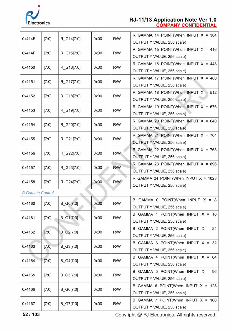
R Gamma Control
0x4140 [7:0] R_G0[7:0] 0x00 R/W R GAMMA 0 POINT(When INPUT X = 8
OUTPUT Y VALUE, 256 scale)
0x4141 [7:0] R_G1[7:0] 0x00 R/W R GAMMA 1 POINT(When INPUT X = 16
OUTPUT Y VALUE, 256 scale)
0x4142 [7:0] R_G2[7:0] 0x00 R/W R GAMMA 2 POINT(When INPUT X = 24
OUTPUT Y VALUE, 256 scale)
0x4143 [7:0] R_G3[7:0] 0x00 R/W R GAMMA 3 POINT(When INPUT X = 32
OUTPUT Y VALUE, 256 scale)
0x4144 [7:0] R_G4[7:0] 0x00 R/W R GAMMA 4 POINT(When INPUT X = 64
OUTPUT Y VALUE, 256 scale)
0x4145 [7:0] R_G5[7:0] 0x00 R/W R GAMMA 5 POINT(When INPUT X = 96
OUTPUT Y VALUE, 256 scale)
0x4146 [7:0] R_G6[7:0] 0x00 R/W R GAMMA 6 POINT(When INPUT X = 128
OUTPUT Y VALUE, 256 scale)
0x4147 [7:0] R_G7[7:0] 0x00 R/W R GAMMA 7 POINT(When INPUT X = 160
OUTPUT Y VALUE, 256 scale)
0x4148 [7:0] R_G8[7:0] 0x00 R/W R GAMMA 8 POINT(When INPUT X = 192
OUTPUT Y VALUE, 256 scale)
0x4149 [7:0] R_G9[7:0] 0x00 R/W R GAMMA 9 POINT(When INPUT X = 224
OUTPUT Y VALUE, 256 scale)
0x414A [7:0] R_G10[7:0] 0x00 R/W R GAMMA 10 POINT(When INPUT X = 256
OUTPUT Y VALUE, 256 scale)
0x414B [7:0] R_G11[7:0] 0x00 R/W R GAMMA 11 POINT(When INPUT X = 288
OUTPUT Y VALUE, 256 scale)
0x414C [7:0] R_G12[7:0] 0x00 R/W R GAMMA 12 POINT(When INPUT X = 320
OUTPUT Y VALUE, 256 scale)
0x414D [7:0] R_G13[7:0] 0x00 R/W R GAMMA 13 POINT(When INPUT X = 352
OUTPUT Y VALUE, 256 scale)
RJ-11/13 Application Note Ver 1.0 COMPANY CONFIDENTIAL
Copyright @ RJ Electronics. All rights reserved. 52 / 103
0x414E [7:0] R_G14[7:0] 0x00 R/W R GAMMA 14 POINT(When INPUT X = 384
OUTPUT Y VALUE, 256 scale)
0x414F [7:0] R_G15[7:0] 0x00 R/W R GAMMA 15 POINT(When INPUT X = 416
OUTPUT Y VALUE, 256 scale)
0x4150 [7:0] R_G16[7:0] 0x00 R/W R GAMMA 16 POINT(When INPUT X = 448
OUTPUT Y VALUE, 256 scale)
0x4151 [7:0] R_G17[7:0] 0x00 R/W R GAMMA 17 POINT(When INPUT X = 480
OUTPUT Y VALUE, 256 scale)
0x4152 [7:0] R_G18[7:0] 0x00 R/W R GAMMA 18 POINT(When INPUT X = 512
OUTPUT Y VALUE, 256 scale)
0x4153 [7:0] R_G19[7:0] 0x00 R/W R GAMMA 19 POINT(When INPUT X = 576
OUTPUT Y VALUE, 256 scale)
0x4154 [7:0] R_G20[7:0] 0x00 R/W R GAMMA 20 POINT(When INPUT X = 640
OUTPUT Y VALUE, 256 scale)
0x4155 [7:0] R_G21[7:0] 0x00 R/W R GAMMA 21 POINT(When INPUT X = 704
OUTPUT Y VALUE, 256 scale)
0x4156 [7:0] R_G22[7:0] 0x00 R/W R GAMMA 22 POINT(When INPUT X = 768
OUTPUT Y VALUE, 256 scale)
0x4157 [7:0] R_G23[7:0] 0x00 R/W R GAMMA 23 POINT(When INPUT X = 896
OUTPUT Y VALUE, 256 scale)
0x4158 [7:0] R_G24[7:0] 0x00 R/W R GAMMA 24 POINT(When INPUT X = 1023
OUTPUT Y VALUE, 256 scale)
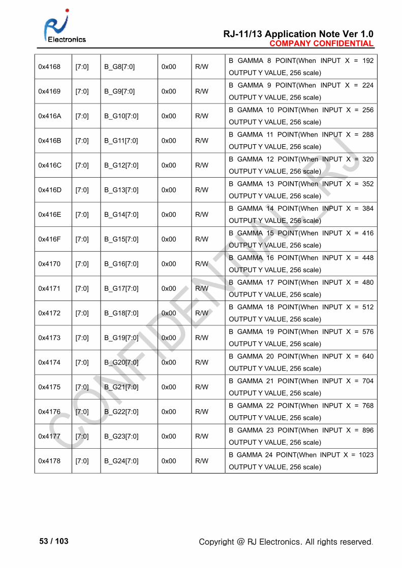
B Gamma Control
0x4160 [7:0] B_G0[7:0] 0x00 R/W B GAMMA 0 POINT(When INPUT X = 8
OUTPUT Y VALUE, 256 scale)
0x4161 [7:0] B_G1[7:0] 0x00 R/W B GAMMA 1 POINT(When INPUT X = 16
OUTPUT Y VALUE, 256 scale)
0x4162 [7:0] B_G2[7:0] 0x00 R/W B GAMMA 2 POINT(When INPUT X = 24
OUTPUT Y VALUE, 256 scale)
0x4163 [7:0] B_G3[7:0] 0x00 R/W B GAMMA 3 POINT(When INPUT X = 32
OUTPUT Y VALUE, 256 scale)
0x4164 [7:0] B_G4[7:0] 0x00 R/W B GAMMA 4 POINT(When INPUT X = 64
OUTPUT Y VALUE, 256 scale)
0x4165 [7:0] B_G5[7:0] 0x00 R/W B GAMMA 5 POINT(When INPUT X = 96
OUTPUT Y VALUE, 256 scale)
0x4166 [7:0] B_G6[7:0] 0x00 R/W B GAMMA 6 POINT(When INPUT X = 128
OUTPUT Y VALUE, 256 scale)
0x4167 [7:0] B_G7[7:0] 0x00 R/W B GAMMA 7 POINT(When INPUT X = 160
OUTPUT Y VALUE, 256 scale)
RJ-11/13 Application Note Ver 1.0 COMPANY CONFIDENTIAL
Copyright @ RJ Electronics. All rights reserved. 53 / 103
0x4168 [7:0] B_G8[7:0] 0x00 R/W B GAMMA 8 POINT(When INPUT X = 192
OUTPUT Y VALUE, 256 scale)
0x4169 [7:0] B_G9[7:0] 0x00 R/W B GAMMA 9 POINT(When INPUT X = 224
OUTPUT Y VALUE, 256 scale)
0x416A [7:0] B_G10[7:0] 0x00 R/W B GAMMA 10 POINT(When INPUT X = 256
OUTPUT Y VALUE, 256 scale)
0x416B [7:0] B_G11[7:0] 0x00 R/W B GAMMA 11 POINT(When INPUT X = 288
OUTPUT Y VALUE, 256 scale)
0x416C [7:0] B_G12[7:0] 0x00 R/W B GAMMA 12 POINT(When INPUT X = 320
OUTPUT Y VALUE, 256 scale)
0x416D [7:0] B_G13[7:0] 0x00 R/W B GAMMA 13 POINT(When INPUT X = 352
OUTPUT Y VALUE, 256 scale)
0x416E [7:0] B_G14[7:0] 0x00 R/W B GAMMA 14 POINT(When INPUT X = 384
OUTPUT Y VALUE, 256 scale)
0x416F [7:0] B_G15[7:0] 0x00 R/W B GAMMA 15 POINT(When INPUT X = 416
OUTPUT Y VALUE, 256 scale)
0x4170 [7:0] B_G16[7:0] 0x00 R/W B GAMMA 16 POINT(When INPUT X = 448
OUTPUT Y VALUE, 256 scale)
0x4171 [7:0] B_G17[7:0] 0x00 R/W B GAMMA 17 POINT(When INPUT X = 480
OUTPUT Y VALUE, 256 scale)
0x4172 [7:0] B_G18[7:0] 0x00 R/W B GAMMA 18 POINT(When INPUT X = 512
OUTPUT Y VALUE, 256 scale)
0x4173 [7:0] B_G19[7:0] 0x00 R/W B GAMMA 19 POINT(When INPUT X = 576
OUTPUT Y VALUE, 256 scale)
0x4174 [7:0] B_G20[7:0] 0x00 R/W B GAMMA 20 POINT(When INPUT X = 640
OUTPUT Y VALUE, 256 scale)
0x4175 [7:0] B_G21[7:0] 0x00 R/W B GAMMA 21 POINT(When INPUT X = 704
OUTPUT Y VALUE, 256 scale)
0x4176 [7:0] B_G22[7:0] 0x00 R/W B GAMMA 22 POINT(When INPUT X = 768
OUTPUT Y VALUE, 256 scale)
0x4177 [7:0] B_G23[7:0] 0x00 R/W B GAMMA 23 POINT(When INPUT X = 896
OUTPUT Y VALUE, 256 scale)
0x4178 [7:0] B_G24[7:0] 0x00 R/W B GAMMA 24 POINT(When INPUT X = 1023
OUTPUT Y VALUE, 256 scale)
RJ-11/13 Application Note Ver 1.0 COMPANY CONFIDENTIAL
Copyright @ RJ Electronics. All rights reserved. 54 / 103
RJ-11/13_Encoder APPLICATION NOTE Ver 1.0
RJ-11/13
Document #: RJ11/13-A01

RJ-11/13 Application Note Ver 1.0 COMPANY CONFIDENTIAL
Copyright @ RJ Electronics. All rights reserved. 55 / 103
REVISION HISTORY
VERSION : Ver 1.0
DATE ;
Author ;
APPROVER ;
Description
ORIGINAL

RJ-11/13 Application Note Ver 1.0 COMPANY CONFIDENTIAL
Copyright @ RJ Electronics. All rights reserved. 56 / 103
This document contains information on a new product. Specifications and information herein are subject to
change without notice.
Use of this specification for product design requires an executed license agreement from RJ Electonics.
RJ Electronics shall not be liable for technical or editorial errors or omissions contained herein; nor for incidental
or consequential damages resulting from the furnishing, performance, or use of this material. Copyright law
protects all parts of the RJ Specification and all rights are reserved. This documentation may not, in whole or in
part, be copied, photocopied, reproduced, translated, or reduced to any electronic medium or machine readable
form without prior consent, in writing, from RJ Electronics.
RJ-11/13 Application Note Ver 1.0 COMPANY CONFIDENTIAL
Copyright @ RJ Electronics. All rights reserved. 57 / 103
TABLE OF CONTENTS
CONTENTS REVISION HISTORY .......................................................................................................................................................... 55
TABLE OF CONTENTS ...................................................................................................................................................... 57
1. Encoder Control ............................................................................................................................................................ 58
1.1 Video Output ............................................................................................................................................................ 58
● Burst Level Control ............................................................................................................................................ 58
● Burst_delay Control ........................................................................................................................................... 58
● Sync Level Control ............................................................................................................................................. 59
● Black Level Control ............................................................................................................................................ 59
RJ-11/13 Application Note Ver 1.0 COMPANY CONFIDENTIAL
Copyright @ RJ Electronics. All rights reserved. 58 / 103
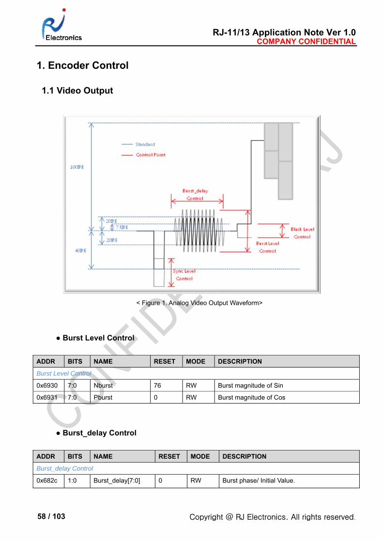
1. Encoder Control
1.1 Video Output
< Figure 1. Analog Video Output Waveform>
● Burst Level Control
ADDR BITS NAME RESET MODE DESCRIPTION
Burst Level Control
0x6930 7:0 Nburst 76 RW Burst magnitude of Sin
0x6931 7:0 Pburst 0 RW Burst magnitude of Cos
● Burst_delay Control
ADDR BITS NAME RESET MODE DESCRIPTION
Burst_delay Control
0x682c 1:0 Burst_delay[7:0] 0 RW Burst phase/ Initial Value.
RJ-11/13 Application Note Ver 1.0 COMPANY CONFIDENTIAL
Copyright @ RJ Electronics. All rights reserved. 59 / 103
● Sync Level Control
ADDR BITS NAME RESET MODE DESCRIPTION
Sync Level Control
0x6913 4:0 Sync level 16 RW Sync level
● Black Level Control
ADDR BITS NAME RESET MODE DESCRIPTION
Black Level Control
0x6912 7:0 Black level 60 RW Black level
RJ-11/13 Application Note Ver 1.0 COMPANY CONFIDENTIAL
Copyright @ RJ Electronics. All rights reserved. 60 / 103
RJ-11/13_AE APPLICATION NOTE Ver 1.0
RJ-11/13
Document #: RJ11/13-A01
RJ-11/13 Application Note Ver 1.0 COMPANY CONFIDENTIAL
Copyright @ RJ Electronics. All rights reserved. 61 / 103
REVISION HISTORY
VERSION : Ver 1.0
DATE ;
Auther ;
APPROVER ;
Descriptipon
ORIGINAL

RJ-11/13 Application Note Ver 1.0 COMPANY CONFIDENTIAL
Copyright @ RJ Electronics. All rights reserved. 62 / 103
This document contains information on a new product. Specifications and information herein are subject to
change without notice.
Use of this specification for product design requires an executed license agreement from RJ Electronics.
RJ Electronics shall not be liable for technical or editorial errors or omissions contained herein; nor for incidental
or consequential damages resulting from the furnishing, performance, or use of this material. Copyright law
protects all parts of the RJ Specification and all rights are reserved. This documentation may not, in whole or in
part, be copied, photocopied, reproduced, translated, or reduced to any electronic medium or machine readable
form without prior consent, in writing, from RJ Electronics.
RJ-11/13 Application Note Ver 1.0 COMPANY CONFIDENTIAL
Copyright @ RJ Electronics. All rights reserved. 63 / 103
TABLE OF CONTENTS
CONTENTS REVISION HISTORY .......................................................................................................................................................... 61
TABLE OF CONTENTS ...................................................................................................................................................... 63
1. AE Operation ................................................................................................................................................................. 64
1.1 AE Operation Processing Flow .............................................................................................................................. 64
1.2 AE Operation Processing Control.......................................................................................................................... 64
● Window ............................................................................................................................................................... 65
● AE Area Register Setting ................................................................................................................................... 66
RJ-11/13 Application Note Ver 1.0 COMPANY CONFIDENTIAL
Copyright @ RJ Electronics. All rights reserved. 64 / 103
1. AE Operation
1.1 AE Operation Processing Flow
< Figure 1. AE Operation Processing Flow>
1.2 AE Operation Processing Control
RJ-11/13 Application Note Ver 1.0 COMPANY CONFIDENTIAL
Copyright @ RJ Electronics. All rights reserved. 65 / 103
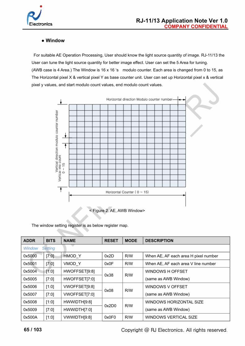
● Window
For suitable AE Operation Processing, User should know the light source quantity of image. RJ-11/13 the
User can tune the light source quantity for better image effect. User can set the 5 Area for tuning.
(AWB case is 4 Area.) The Window is 16 x 16 ‘s modulo counter. Each area is changed from 0 to 15, as
The Horizontal pixel X & vertical pixel Y as base counter unit. User can set up Horizontal pixel x & vertical
pixel y values, and start modulo count values, end modulo count values.
< Figure 2. AE, AWB Window>
The window setting register is as below register map.
ADDR BITS NAME RESET MODE DESCRIPTION
Window Setting
0x5000 [7:0] HMOD_Y 0x2D R/W When AE, AF each area H pixel number
0x5001 [7:0] VMOD_Y 0x0F R/W When AE, AF each area V line number
0x5004 [1:0] HWOFFSET[9:8] 0x38 R/W
WINDOWS H OFFSET
(same as AWB Window) 0x5005 [7:0] HWOFFSET[7:0]
0x5006 [1:0] VWOFFSET[9:8] 0x08 R/W
WINDOWS V OFFSET
(same as AWB Window) 0x5007 [7:0] VWOFFSET[7:0]
0x5008 [1:0] HWWIDTH[9:8] 0x2D0 R/W
WINDOWS HORIZONTAL SIZE
(same as AWB Window) 0x5009 [7:0] HWWIDTH[7:0]
0x500A [1:0] VWWIDTH[9:8] 0x0F0 R/W WINDOWS VERTICAL SIZE
RJ-11/13 Application Note Ver 1.0 COMPANY CONFIDENTIAL
Copyright @ RJ Electronics. All rights reserved. 66 / 103
0x500B [7:0] VWWIDTH[7:0] (same as AWB Window)
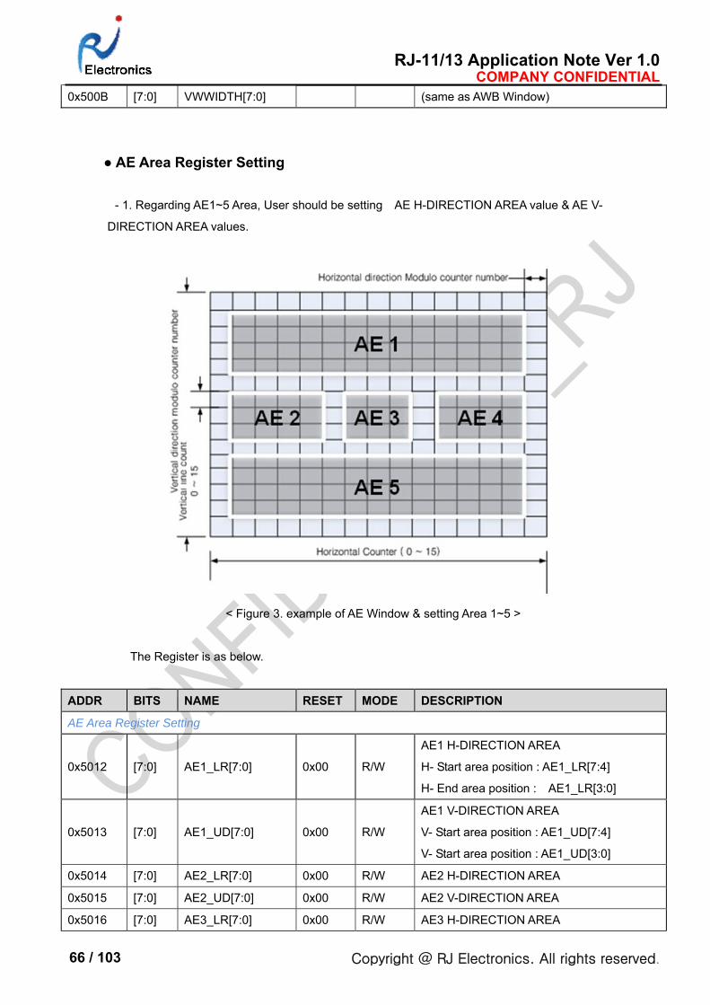
● AE Area Register Setting
- 1. Regarding AE1~5 Area, User should be setting AE H-DIRECTION AREA value & AE V-
DIRECTION AREA values.
< Figure 3. example of AE Window & setting Area 1~5 >
The Register is as below.
ADDR BITS NAME RESET MODE DESCRIPTION
AE Area Register Setting
0x5012 [7:0] AE1_LR[7:0] 0x00 R/W
AE1 H-DIRECTION AREA
H- Start area position : AE1_LR[7:4]
H- End area position : AE1_LR[3:0]
0x5013 [7:0] AE1_UD[7:0] 0x00 R/W
AE1 V-DIRECTION AREA
V- Start area position : AE1_UD[7:4]
V- Start area position : AE1_UD[3:0]
0x5014 [7:0] AE2_LR[7:0] 0x00 R/W AE2 H-DIRECTION AREA
0x5015 [7:0] AE2_UD[7:0] 0x00 R/W AE2 V-DIRECTION AREA
0x5016 [7:0] AE3_LR[7:0] 0x00 R/W AE3 H-DIRECTION AREA
RJ-11/13 Application Note Ver 1.0 COMPANY CONFIDENTIAL
Copyright @ RJ Electronics. All rights reserved. 67 / 103
0x5017 [7:0] AE3_UD[7:0] 0x00 R/W AE3 V-DIRECTION AREA
0x5018 [7:0] AE4_LR[7:0] 0x00 R/W AE4 H-DIRECTION AREA
0x5019 [7:0] AE4_UD[7:0] 0x00 R/W AE4 V-DIRECTION AREA
0x501A [7:0] AE5_LR[7:0] 0x00 R/W AE5 H-DIRECTION AREA
0x501B [7:0] AE5_UD[7:0] 0x00 R/W AE5 V-DIRECTION AREA
- 2. Regarding AE Operation, User can check the Y Summation values in each area.
AE Data’s Output Parameter values as below.
ADDR BITS NAME RESET MODE DESCRIPTION
AE Y Summation Value
0x5500 [7:0] AE1_SUM[31:24]
- R AE1_SUM 0x5501 [7:0] AE1_SUM[23:16]
0x5502 [7:0] AE1_SUM[15:8]
0x5503 [7:0] AE1_SUM[7:0]
0x5504 [7:0] AE2_SUM[31:24]
- R AE2_SUM 0x5505 [7:0] AE2_SUM[23:16]
0x5506 [7:0] AE2_SUM[15:8]
0x5507 [7:0] AE2_SUM[7:0]
0x5508 [7:0] AE3_SUM[31:24]
- R AE3_SUM 0x5509 [7:0] AE3_SUM[23:16]
0x550A [7:0] AE3_SUM[15:8]
0x550B [7:0] AE3_SUM[7:0]
0x550C [7:0] AE4_SUM[31:24]
- R
AE4_SUM
0x550D [7:0] AE4_SUM[23:16]
0x550E [7:0] AE4_SUM[15:8]
0x550F [7:0] AE4_SUM[7:0]
0x5510 [7:0] AE5_SUM[31:24]
- R AE5_SUM 0x5511 [7:0] AE5_SUM[23:16]
0x5512 [7:0] AE5_SUM[15:8]
0x5513 [7:0] AE5_SUM[7:0]
- 3. Regarding AE Operation, the each Area Histogram values as below.
ADDR BITS NAME RESET MODE DESCRIPTION
Histogram Setting
0x5010 [3:0] HIST_AREA 0x00 R/W WINDOWS SELECT (AE1~AE5 select one)
0x5011 [1:0] HIST_MODE 0x00 R/W HISTOGRAM value setting
AE Y Histogram Value
RJ-11/13 Application Note Ver 1.0 COMPANY CONFIDENTIAL
Copyright @ RJ Electronics. All rights reserved. 68 / 103
0x5514 [7:0] HIST_SUM1[23:16]
- R HISTOGRAM STEP 1 SUM OUT 0x5515 [7:0] HIST_SUM1[15:8]
0x5516 [7:0] HIST_SUM1[7:0]
0x5517 [7:0] HIST_SUM2[23:16]
- R HISTOGRAM STEP 2 SUM OUT 0x5518 [7:0] HIST_SUM2[15:8]
0x5519 [7:0] HIST_SUM2[7:0]
0x551A [7:0] HIST_SUM3[23:16]
- R HISTOGRAM STEP 3 SUM OUT 0x551B [7:0] HIST_SUM3[15:8]
0x551C [7:0] HIST_SUM3[7:0]
0x551D [7:0] HIST_SUM4[23:16]
- R HISTOGRAM STEP 4 SUM OUT 0x551E [7:0] HIST_SUM4[15:8]
0x551F [7:0] HIST_SUM4[7:0]
0x5520 [7:0] HIST_SUM5[23:16]
- R HISTOGRAM STEP 5 SUM OUT 0x5521 [7:0] HIST_SUM5[15:8]
0x5522 [7:0] HIST_SUM5[7:0]
0x5523 [7:0] HIST_SUM6[23:16]
- R HISTOGRAM STEP 6 SUM OUT 0x5524 [7:0] HIST_SUM6[15:8]
0x5525 [7:0] HIST_SUM6[7:0]
0x5526 [7:0] HIST_SUM7[23:16]
- R HISTOGRAM STEP 7 SUM OUT 0x5527 [7:0] HIST_SUM7[15:8]
0x5528 [7:0] HIST_SUM7[7:0]
0x5529 [7:0] HIST_SUM8[23:16]
- R HISTOGRAM STEP 8 SUM OUT 0x552A [7:0] HIST_SUM8[15:8]
0x552B [7:0] HIST_SUM8[7:0]
0x552C [7:0] HIST_SUM9[23:16]
- R HISTOGRAM STEP 9 SUM OUT 0x552D [7:0] HIST_SUM9[15:8]
0x552E [7:0] HIST_SUM9[7:0]
0x552F [7:0] HIST_SUM10[23:16]
- R HISTOGRAM STEP 10 SUM OUT 0x5530 [7:0] HIST_SUM10[15:8]
0x5531 [7:0] HIST_SUM10[7:0]
0x5532 [7:0] HIST_SUM11[23:16]
- R HISTOGRAM STEP 11 SUM OUT 0x5533 [7:0] HIST_SUM11[15:8]
0x5534 [7:0] HIST_SUM11[7:0]
0x5535 [7:0] HIST_SUM12[23:16]
- R HISTOGRAM STEP 12 SUM OUT 0x5536 [7:0] HIST_SUM12[15:8]
0x5537 [7:0] HIST_SUM12[7:0]
0x5538 [7:0] HIST_SUM13[23:16] - R HISTOGRAM STEP 13 SUM OUT
0x5539 [7:0] HIST_SUM13[15:8]
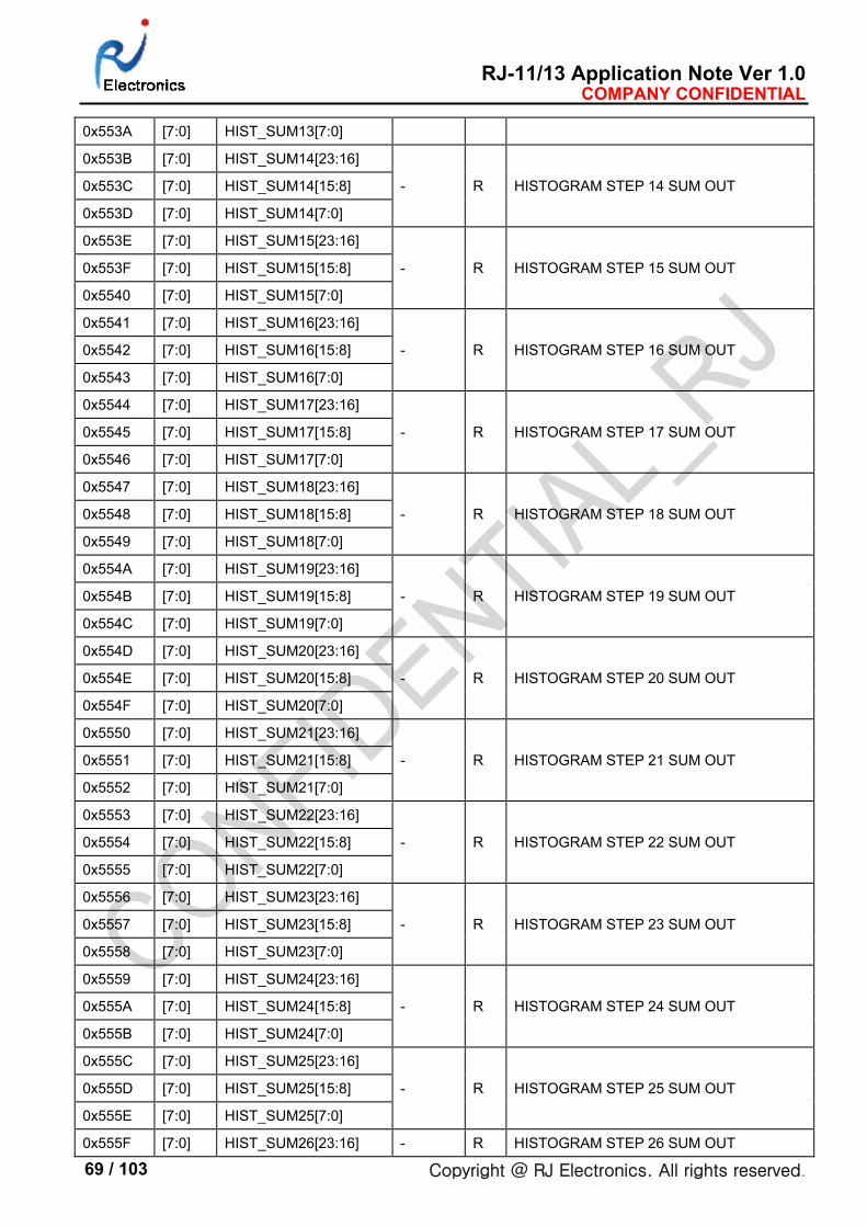
RJ-11/13 Application Note Ver 1.0 COMPANY CONFIDENTIAL
Copyright @ RJ Electronics. All rights reserved. 69 / 103
0x553A [7:0] HIST_SUM13[7:0]
0x553B [7:0] HIST_SUM14[23:16]
- R HISTOGRAM STEP 14 SUM OUT 0x553C [7:0] HIST_SUM14[15:8]
0x553D [7:0] HIST_SUM14[7:0]
0x553E [7:0] HIST_SUM15[23:16]
- R HISTOGRAM STEP 15 SUM OUT 0x553F [7:0] HIST_SUM15[15:8]
0x5540 [7:0] HIST_SUM15[7:0]
0x5541 [7:0] HIST_SUM16[23:16]
- R HISTOGRAM STEP 16 SUM OUT 0x5542 [7:0] HIST_SUM16[15:8]
0x5543 [7:0] HIST_SUM16[7:0]
0x5544 [7:0] HIST_SUM17[23:16]
- R HISTOGRAM STEP 17 SUM OUT 0x5545 [7:0] HIST_SUM17[15:8]
0x5546 [7:0] HIST_SUM17[7:0]
0x5547 [7:0] HIST_SUM18[23:16]
- R HISTOGRAM STEP 18 SUM OUT 0x5548 [7:0] HIST_SUM18[15:8]
0x5549 [7:0] HIST_SUM18[7:0]
0x554A [7:0] HIST_SUM19[23:16]
- R HISTOGRAM STEP 19 SUM OUT 0x554B [7:0] HIST_SUM19[15:8]
0x554C [7:0] HIST_SUM19[7:0]
0x554D [7:0] HIST_SUM20[23:16]
- R HISTOGRAM STEP 20 SUM OUT 0x554E [7:0] HIST_SUM20[15:8]
0x554F [7:0] HIST_SUM20[7:0]
0x5550 [7:0] HIST_SUM21[23:16]
- R HISTOGRAM STEP 21 SUM OUT 0x5551 [7:0] HIST_SUM21[15:8]
0x5552 [7:0] HIST_SUM21[7:0]
0x5553 [7:0] HIST_SUM22[23:16]
- R HISTOGRAM STEP 22 SUM OUT 0x5554 [7:0] HIST_SUM22[15:8]
0x5555 [7:0] HIST_SUM22[7:0]
0x5556 [7:0] HIST_SUM23[23:16]
- R HISTOGRAM STEP 23 SUM OUT 0x5557 [7:0] HIST_SUM23[15:8]
0x5558 [7:0] HIST_SUM23[7:0]
0x5559 [7:0] HIST_SUM24[23:16]
- R HISTOGRAM STEP 24 SUM OUT 0x555A [7:0] HIST_SUM24[15:8]
0x555B [7:0] HIST_SUM24[7:0]
0x555C [7:0] HIST_SUM25[23:16]
- R HISTOGRAM STEP 25 SUM OUT 0x555D [7:0] HIST_SUM25[15:8]
0x555E [7:0] HIST_SUM25[7:0]
0x555F [7:0] HIST_SUM26[23:16] - R HISTOGRAM STEP 26 SUM OUT
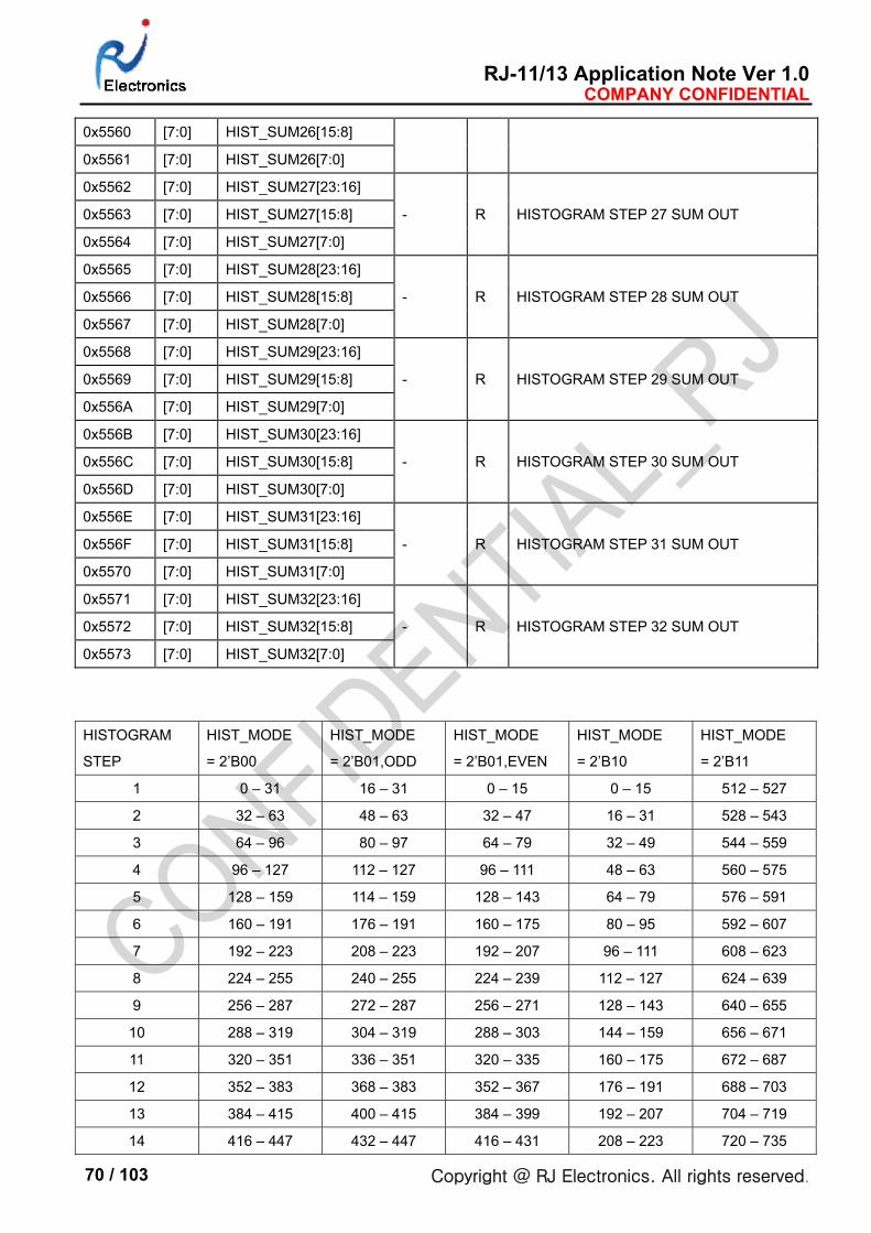
RJ-11/13 Application Note Ver 1.0 COMPANY CONFIDENTIAL
Copyright @ RJ Electronics. All rights reserved. 70 / 103
0x5560 [7:0] HIST_SUM26[15:8]
0x5561 [7:0] HIST_SUM26[7:0]
0x5562 [7:0] HIST_SUM27[23:16]
- R HISTOGRAM STEP 27 SUM OUT 0x5563 [7:0] HIST_SUM27[15:8]
0x5564 [7:0] HIST_SUM27[7:0]
0x5565 [7:0] HIST_SUM28[23:16]
- R HISTOGRAM STEP 28 SUM OUT 0x5566 [7:0] HIST_SUM28[15:8]
0x5567 [7:0] HIST_SUM28[7:0]
0x5568 [7:0] HIST_SUM29[23:16]
- R HISTOGRAM STEP 29 SUM OUT 0x5569 [7:0] HIST_SUM29[15:8]
0x556A [7:0] HIST_SUM29[7:0]
0x556B [7:0] HIST_SUM30[23:16]
- R HISTOGRAM STEP 30 SUM OUT 0x556C [7:0] HIST_SUM30[15:8]
0x556D [7:0] HIST_SUM30[7:0]
0x556E [7:0] HIST_SUM31[23:16]
- R HISTOGRAM STEP 31 SUM OUT 0x556F [7:0] HIST_SUM31[15:8]
0x5570 [7:0] HIST_SUM31[7:0]
0x5571 [7:0] HIST_SUM32[23:16]
- R HISTOGRAM STEP 32 SUM OUT 0x5572 [7:0] HIST_SUM32[15:8]
0x5573 [7:0] HIST_SUM32[7:0]
HISTOGRAM
STEP
HIST_MODE
= 2’B00
HIST_MODE
= 2’B01,ODD
HIST_MODE
= 2’B01,EVEN
HIST_MODE
= 2’B10
HIST_MODE
= 2’B11
1 0 – 31 16 – 31 0 – 15 0 – 15 512 – 527
2 32 – 63 48 – 63 32 – 47 16 – 31 528 – 543
3 64 – 96 80 – 97 64 – 79 32 – 49 544 – 559
4 96 – 127 112 – 127 96 – 111 48 – 63 560 – 575
5 128 – 159 114 – 159 128 – 143 64 – 79 576 – 591
6 160 – 191 176 – 191 160 – 175 80 – 95 592 – 607
7 192 – 223 208 – 223 192 – 207 96 – 111 608 – 623
8 224 – 255 240 – 255 224 – 239 112 – 127 624 – 639
9 256 – 287 272 – 287 256 – 271 128 – 143 640 – 655
10 288 – 319 304 – 319 288 – 303 144 – 159 656 – 671
11 320 – 351 336 – 351 320 – 335 160 – 175 672 – 687
12 352 – 383 368 – 383 352 – 367 176 – 191 688 – 703
13 384 – 415 400 – 415 384 – 399 192 – 207 704 – 719
14 416 – 447 432 – 447 416 – 431 208 – 223 720 – 735
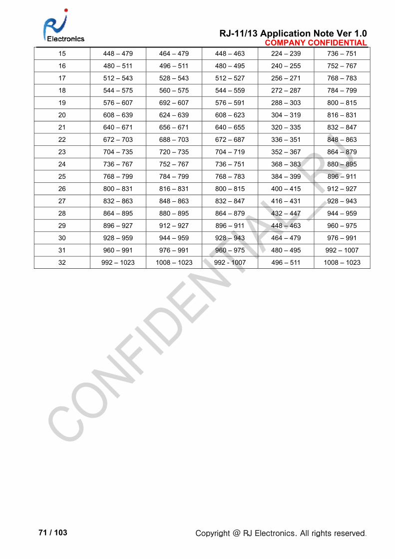
RJ-11/13 Application Note Ver 1.0 COMPANY CONFIDENTIAL
Copyright @ RJ Electronics. All rights reserved. 71 / 103
15 448 – 479 464 – 479 448 – 463 224 – 239 736 – 751
16 480 – 511 496 – 511 480 – 495 240 – 255 752 – 767
17 512 – 543 528 – 543 512 – 527 256 – 271 768 – 783
18 544 – 575 560 – 575 544 – 559 272 – 287 784 – 799
19 576 – 607 692 – 607 576 – 591 288 – 303 800 – 815
20 608 – 639 624 – 639 608 – 623 304 – 319 816 – 831
21 640 – 671 656 – 671 640 – 655 320 – 335 832 – 847
22 672 – 703 688 – 703 672 – 687 336 – 351 848 – 863
23 704 – 735 720 – 735 704 – 719 352 – 367 864 – 879
24 736 – 767 752 – 767 736 – 751 368 – 383 880 – 895
25 768 – 799 784 – 799 768 – 783 384 – 399 896 – 911
26 800 – 831 816 – 831 800 – 815 400 – 415 912 – 927
27 832 – 863 848 – 863 832 – 847 416 – 431 928 – 943
28 864 – 895 880 – 895 864 – 879 432 – 447 944 – 959
29 896 – 927 912 – 927 896 – 911 448 – 463 960 – 975
30 928 – 959 944 – 959 928 – 943 464 – 479 976 – 991
31 960 – 991 976 – 991 960 – 975 480 – 495 992 – 1007
32 992 – 1023 1008 – 1023 992 - 1007 496 – 511 1008 – 1023
RJ-11/13 Application Note Ver 1.0 COMPANY CONFIDENTIAL
Copyright @ RJ Electronics. All rights reserved. 72 / 103
RJ-11/13_AWB APPLICATION NOTE Ver 1.0
RJ-11/13
Document #: RJ11/13-A01

RJ-11/13 Application Note Ver 1.0 COMPANY CONFIDENTIAL
Copyright @ RJ Electronics. All rights reserved. 73 / 103
REVISION HISTORY
VERSION : Ver 1.0
DATE ;
Author ;
APPROVER ;
Description
ORIGINAL

RJ-11/13 Application Note Ver 1.0 COMPANY CONFIDENTIAL
Copyright @ RJ Electronics. All rights reserved. 74 / 103
This document contains information on a new product. Specifications and information herein are subject to
change without notice.
Use of this specification for product design requires an executed license agreement from RJ Electronics.
RJ Electronics shall not be liable for technical or editorial errors or omissions contained herein; nor for incidental
or consequential damages resulting from the furnishing, performance, or use of this material. Copyright law
protects all parts of the RJ Specification and all rights are reserved. This documentation may not, in whole or in
part, be copied, photocopied, reproduced, translated, or reduced to any electronic medium or machine readable
form without prior consent, in writing, from RJ Electronics.
RJ-11/13 Application Note Ver 1.0 COMPANY CONFIDENTIAL
Copyright @ RJ Electronics. All rights reserved. 75 / 103
TABLE OF CONTENTS
CONTENTS REVISION HISTORY .......................................................................................................................................................... 68
TABLE OF CONTENTS ...................................................................................................................................................... 75
1. AWB Operation .............................................................................................................................................................. 75
1.1 AWB Window ............................................................................................................................................................ 76
● Window Setting .................................................................................................................................................. 76
● Y Signal Selection .............................................................................................................................................. 77
1.2 WGA (World Grey Assumption) Operation Processing ....................................................................................... 78
● WGA Area Register Setting ............................................................................................................................... 78
1.3 WPD (White Point Discrimination) Operation Processing ................................................................................... 82
● WPD Area Register Setting ............................................................................................................................... 82
● Luminance Level Setting .................................................................... 오류! 책갈피가 정의되어 있지 않습니다.
● White Table Setting ............................................................................. 오류! 책갈피가 정의되어 있지 않습니다.
1.4 Color Gain Control .................................................................................................................................................. 84
RJ-11/13 Application Note Ver 1.0 COMPANY CONFIDENTIAL
Copyright @ RJ Electronics. All rights reserved. 76 / 103
1. AWB Operation
1.1 AWB Window
● Window Setting
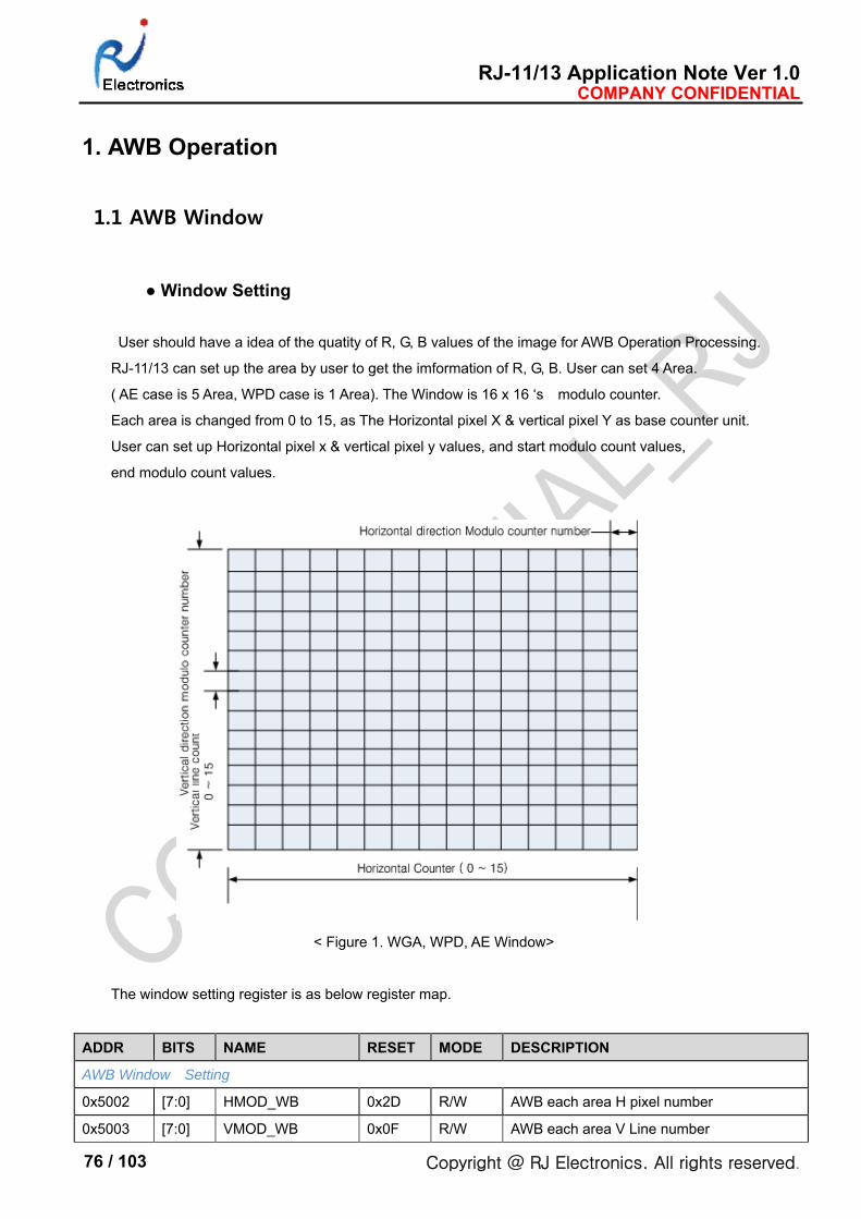
User should have a idea of the quatity of R, G, B values of the image for AWB Operation Processing.
RJ-11/13 can set up the area by user to get the imformation of R, G, B. User can set 4 Area.
( AE case is 5 Area, WPD case is 1 Area). The Window is 16 x 16 ‘s modulo counter.
Each area is changed from 0 to 15, as The Horizontal pixel X & vertical pixel Y as base counter unit.
User can set up Horizontal pixel x & vertical pixel y values, and start modulo count values,
end modulo count values.
< Figure 1. WGA, WPD, AE Window>
The window setting register is as below register map.
ADDR BITS NAME RESET MODE DESCRIPTION
AWB Window Setting
0x5002 [7:0] HMOD_WB 0x2D R/W AWB each area H pixel number
0x5003 [7:0] VMOD_WB 0x0F R/W AWB each area V Line number
RJ-11/13 Application Note Ver 1.0 COMPANY CONFIDENTIAL
Copyright @ RJ Electronics. All rights reserved. 77 / 103
0x5004 [1:0] HWOFFSET[9:8] 0x38 R/W
WINDOWS H OFFSET
(same as AE Window) 0x5005 [7:0] HWOFFSET[7:0]
0x5006 [1:0] VWOFFSET[9:8] 0x08 R/W
WINDOWS V OFFSET
(same as AE Window) 0x5007 [7:0] VWOFFSET[7:0]
0x5008 [1:0] HWWIDTH[9:8] 0x2D0 R/W
WINDOWS HORIZONTAL SIZE
(same as AE Window) 0x5009 [7:0] HWWIDTH[7:0]
0x500A [1:0] VWWIDTH[9:8] 0x0F0 R/W
WINDOWS VERTICAL SIZE
(same as AE Window) 0x500B [7:0] VWWIDTH[7:0]
● Y Signal Selection
-User should select which kind of Algorithm Y for the AWB Operation Processing.
ADDR BITS NAME RESET MODE DESCRIPTION
Luminance Select
0x5060 [2:1] LUM_SELECT 0x00 R/W
Select Y Definition.
2’b00, Y = 0.3R + 0.6G + 0.1B
2’b01, Y = (R + 2*G + B) /4
2’b10, Y = G
2’b11, Y = (R + G + B) / 3
RJ-11/13 Application Note Ver 1.0 COMPANY CONFIDENTIAL
Copyright @ RJ Electronics. All rights reserved. 78 / 103
1.2 WGA (World Grey Assumption) Operation Processing
● WGA Area Register Setting
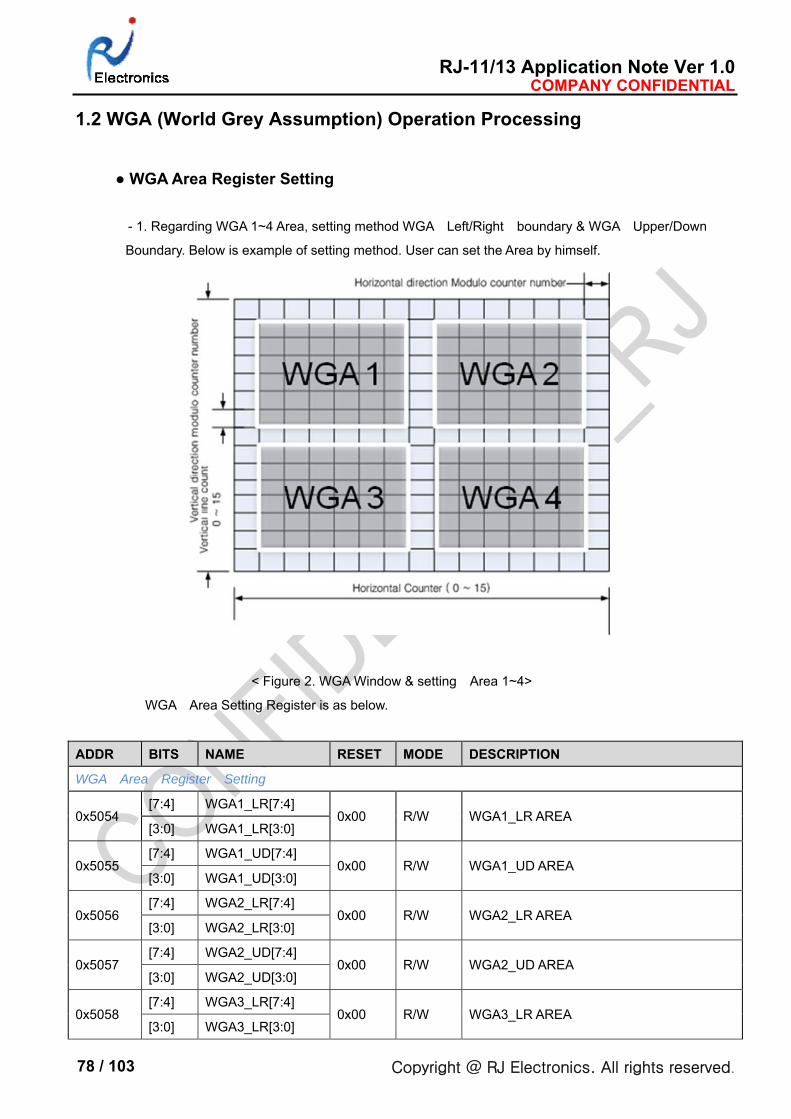
- 1. Regarding WGA 1~4 Area, setting method WGA Left/Right boundary & WGA Upper/Down
Boundary. Below is example of setting method. User can set the Area by himself.
< Figure 2. WGA Window & setting Area 1~4>
WGA Area Setting Register is as below.
ADDR BITS NAME RESET MODE DESCRIPTION
WGA Area Register Setting
0x5054 [7:4] WGA1_LR[7:4]
0x00 R/W WGA1_LR AREA [3:0] WGA1_LR[3:0]
0x5055 [7:4] WGA1_UD[7:4]
0x00 R/W WGA1_UD AREA [3:0] WGA1_UD[3:0]
0x5056 [7:4] WGA2_LR[7:4]
0x00 R/W WGA2_LR AREA [3:0] WGA2_LR[3:0]
0x5057 [7:4] WGA2_UD[7:4]
0x00 R/W WGA2_UD AREA [3:0] WGA2_UD[3:0]
0x5058 [7:4] WGA3_LR[7:4]
0x00 R/W WGA3_LR AREA [3:0] WGA3_LR[3:0]
RJ-11/13 Application Note Ver 1.0 COMPANY CONFIDENTIAL
Copyright @ RJ Electronics. All rights reserved. 79 / 103
0x5059 [7:4] WGA3_UD[7:4]
0x00 R/W WGA3_UD AREA [3:0] WGA3_UD[3:0]
0x505A [7:4] WGA4_LR[7:4]
0x00 R/W WGA4_LR AREA [3:0] WGA4_LR[3:0]
0x505B [7:4] WGA4_UD[7:4]
0x00 R/W WGA4_UD AREA [3:0] WGA4_UD[3:0]
- 2. Regarding WGA Operation, we can get the values of each Area R,G,B Summation.
WGA Data Output Parameter values is as below.
ADDR BITS NAME RESET MODE DESCRIPTION
WGA R,G,B Summation Value
0x55BC [7:0] RSUM1[31:24] -
R WGA1 AREA R SUM 0x55BD [7:0] RSUM1[23:16]
0x55BE [7:0] RSUM1[15:8]
0x55BF [7:0] RSUM1[7:0]
0x55C0 [7:0] GSUM1[31:24] -
R WGA1 AREA G SUM 0x55C1 [7:0] GSUM1[23:16]
0x55C2 [7:0] GSUM1[15:8]
0x55C3 [7:0] GSUM1[7:0]
0x55C4 [7:0] BSUM1[31:24] -
R WGA1 AREA B SUM 0x55C5 [7:0] BSUM1[23:16]
0x55C6 [7:0] BSUM1[15:8]
0x55C7 [7:0] BSUM1[7:0]
0x55C8 [7:0] RSUM2[31:24] -
R WGA2 AREA R SUM 0x55C9 [7:0] RSUM2[23:16]
0x55CA [7:0] RSUM2[15:8]
0x55CB [7:0] RSUM2[7:0]
0x55CC [7:0] GSUM2[31:24] -
R WGA2 AREA G SUM 0x55CD [7:0] GSUM2[23:16]
0x55CE [7:0] GSUM2[15:8]
0x55CF [7:0] GSUM2[7:0]
0x55D0 [7:0] BSUM2[31:24] -
R WGA2 AREA B SUM 0x55D1 [7:0] BSUM2[23:16]
0x55D2 [7:0] BSUM2[15:8]
0x55D3 [7:0] BSUM2[7:0]
0x55D4 [7:0] RSUM3[31:24] -
R WGA3 AREA R SUM 0x55D5 [7:0] RSUM3[23:16]
0x55D6 [7:0] RSUM3[15:8]
RJ-11/13 Application Note Ver 1.0 COMPANY CONFIDENTIAL
Copyright @ RJ Electronics. All rights reserved. 80 / 103
0x55D7 [7:0] RSUM3[7:0]
0x55D8 [7:0] GSUM3[31:24] -
R WGA3 AREA G SUM 0x55D9 [7:0] GSUM3[23:16]
0x55DA [7:0] GSUM3[15:8]
0x55DB [7:0] GSUM3[7:0]
0x55DC [7:0] BSUM3[31:24] -
R WGA3 AREA B SUM 0x55DD [7:0] BSUM3[23:16]
0x55DE [7:0] BSUM3[15:8]
0x55DF [7:0] BSUM3[7:0]
0x55E0 [7:0] RSUM4[31:24] -
R WGA4 AREA R SUM 0x55E1 [7:0] RSUM4[23:16]
0x55E2 [7:0] RSUM4[15:8]
0x55E3 [7:0] RSUM4[7:0]
0x55E4 [7:0] GSUM4[31:24] -
R WGA4 AREA G SUM 0x55E5 [7:0] GSUM4[23:16]
0x55E6 [7:0] GSUM4[15:8]
0x55E7 [7:0] GSUM4[7:0]
0x55E8 [7:0] BSUM4[31:24] -
R WGA4 AREA B SUM 0x55E9 [7:0] BSUM4[23:16]
0x55EA [7:0] BSUM4[15:8]
0x55EB [7:0] BSUM4[7:0]
- 3. Regarding WGA Operation, each Area’s Reference White Pixel values as below.
WGA Data Output Parameter values is as below.
ADDR BITS NAME RESET MODE DESCRIPTION
WGA Reference White Pixels Numbers
0x55EC [7:0] WGA1C[23:16]
- R WGA1 AREA COUNT 0x55ED [7:0] WGA1C[15:8]
0x55EE [7:0] WGA1C[7:0]
0x55EF [7:0] WGA2C[23:16]
- R WGA2 AREA COUNT 0x55F0 [7:0] WGA2C[15:8]
0x55F1 [7:0] WGA2C[7:0]
0x55F2 [7:0] WGA3C[23:16]
- R WGA3 AREA COUNT 0x55F3 [7:0] WGA3C[15:8]
0x55F4 [7:0] WGA3C[7:0]
0x55F5 [7:0] WGA4C[23:16] - R WGA4 AREA COUNT
RJ-11/13 Application Note Ver 1.0 COMPANY CONFIDENTIAL
Copyright @ RJ Electronics. All rights reserved. 81 / 103
0x55F6 [7:0] WGA4C[15:8]
0x55F7 [7:0] WGA4C[7:0]
RJ-11/13 Application Note Ver 1.0 COMPANY CONFIDENTIAL
Copyright @ RJ Electronics. All rights reserved. 82 / 103
1.3 WPD (White Point Discrimination) Operation Processing
● WPD Area Register Setting
- WPD set up only one WPD Left/Right boundary & WGA Upper/Down boundary.
(As we mentioned, the AE, WGA, WPD has a same Window.)
ADDR BITS NAME RESET MODE DESCRIPTION
AWB Window Setting
0x5002 [7:0] HMOD_WB 0x2D R/W AWB each area H pixel number
0x5003 [7:0] VMOD_WB 0x0F R/W AWB each area V Line number
0x5060 [ 0] WPD _DISP 0x0 R/W WHITE PIXEL DISPLAY ON/OFF
0x5061 [7:0] WPD_LR 0x00 R/W
WPD H-DIRECTION AREA
H- Start area position : WPD_LR[7:4]
H- End area position : WPD_LR[3:0]
0x5062 [7:0] WPD_UD 0x00 R/W
WPD V-DIRECTION AREA
V- Start area position : WPD_UD[7:4]
V- End area position : WPD_UD[3:0]
- Regarding WPD Operation, we can check the each Area R,G,B ,Y Summation & White Pixel number.
The WPD Data Output Parameter values is as below.
ADDR BITS NAME RESET MODE DESCRIPTION
WPD R,G,B Summation Value
0x55F8 [7:0] WPD_R[31:24]
- R WHITE PIXEL R SUM 0x55F9 [7:0] WPD_R[23:16]
0x55FA [7:0] WPD_R[15:8]
0x55FB [7:0] WPD_R[7:0]
0x55FC [7:0] WPD_G[31:24]
- R WHITE PIXEL G SUM 0x55FD [7:0] WPD_G[23:16]
0x55FE [7:0] WPD_G[15:8]
0x55FF [7:0] WPD_G[7:0]
0x5600 [7:0] WPD_B[31:24]
- R WHITE PIXEL B SUM 0x5601 [7:0] WPD_B[23:16]
0x5602 [7:0] WPD_B[15:8]
0x5603 [7:0] WPD_B[7:0]
0x5604 [7:0] WPD_Y[31:24] - R WHITE PIXEL Y SUM
0x5605 [7:0] WPD_Y[23:16]
RJ-11/13 Application Note Ver 1.0 COMPANY CONFIDENTIAL
Copyright @ RJ Electronics. All rights reserved. 83 / 103
0x5606 [7:0] WPD_Y[15:8]
0x5607 [7:0] WPD_Y[7:0]
0x5608 [7:0] WPD_C[23:16]
- R WHITE PIXEL Y SUM 0x5609 [7:0] WPD_C[15:8]
0x560A [7:0] WPD_C[7:0]
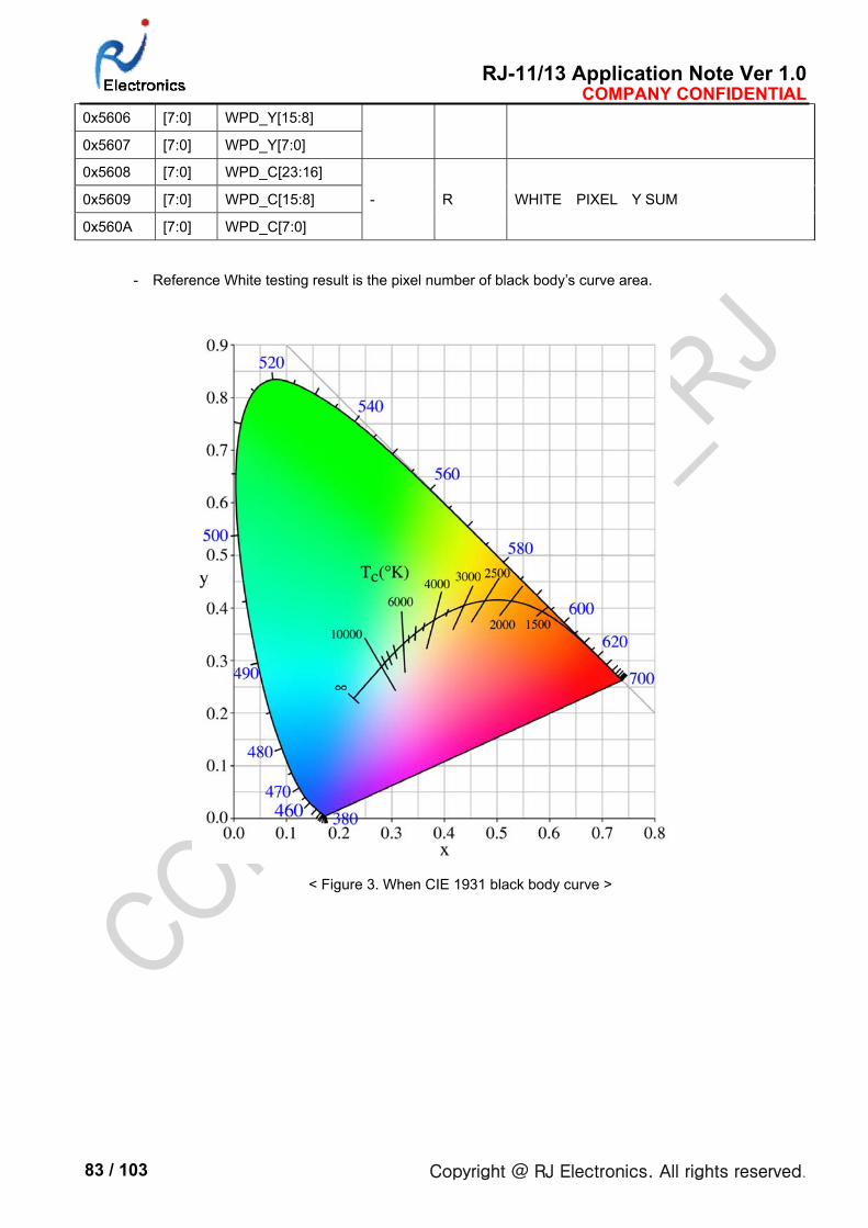
- Reference White testing result is the pixel number of black body’s curve area.
< Figure 3. When CIE 1931 black body curve >
RJ-11/13 Application Note Ver 1.0 COMPANY CONFIDENTIAL
Copyright @ RJ Electronics. All rights reserved. 84 / 103
1.4 Color Gain Control
After AWB Setting, User can change the Gain values of color to get their request.
ADDR BITS NAME RESET MODE DESCRIPTION
Color Gain Control After AWB Setting
0x4109 [7:0] G_AWBG 0x00 R/W AWB GAIN OF G
0x410A [7:0] R_AWBG 0x00 R/W AWB GAIN OF R
0x410B [7:0] B_AWBG 0x00 R/W AWB GAIN OF B
RJ-11/13 Application Note Ver 1.0 COMPANY CONFIDENTIAL
Copyright @ RJ Electronics. All rights reserved. 85 / 103
RJ-11/13
HighLight Inversion APPLICATION NOTE Ver 1.0
RJ-11/13
Document #: RJ11/13-A01

RJ-11/13 Application Note Ver 1.0 COMPANY CONFIDENTIAL
Copyright @ RJ Electronics. All rights reserved. 86 / 103
REVISION HISTORY
VERSION : Ver 1.0
DATE ;
Author ;
APPROVER ;
Description
ORIGINAL

RJ-11/13 Application Note Ver 1.0 COMPANY CONFIDENTIAL
Copyright @ RJ Electronics. All rights reserved. 87 / 103
This document contains information on a new product. Specifications and information herein are subject to
change without notice.
Use of this specification for product design requires an executed license agreement from RJ Electronics.
RJ Electronics shall not be liable for technical or editorial errors or omissions contained herein; nor for incidental
or consequential damages resulting from the furnishing, performance, or use of this material. Copyright law
protects all parts of the RJ Specification and all rights are reserved. This documentation may not, in whole or in
part, be copied, photocopied, reproduced, translated, or reduced to any electronic medium or machine readable
form without prior consent, in writing, from RJ Electronics.
RJ-11/13 Application Note Ver 1.0 COMPANY CONFIDENTIAL
Copyright @ RJ Electronics. All rights reserved. 88 / 103
TABLE OF CONTENTS
INDEX REVISION HISTORY .......................................................................................................................................................... 86
TABLE OF CONTENTS ...................................................................................................................................................... 88
1. Highlight Inversion ........................................................................................................................................................ 89
1.1 Highlight Inversion ............................................................................................................................................... 89
1.2 Register ................................................................................................................................................................. 89
RJ-11/13 Application Note Ver 1.0 COMPANY CONFIDENTIAL
Copyright @ RJ Electronics. All rights reserved. 89 / 103
1. Highlight Inversion
1.1 Highlight Inversion
High Luminance image will be effective AE function as making Shutter quickly or reducing the Gain.
If one frame has a very high Luminance values area, AE will make a dark background image for
the very high Luminance area. So that’s why too high Luminiance values make a bad image. We
should make a too high Luminance values reduce to get better image.
1.2 Highlight Inversion Register
RJ-11/13 Highlight Inversion Registeris as below.
ADDR BITS NAME RESET MODE DESCRIPTION
Highlight Inversion
0x4015 1 HILIGHT_CHROMA_OFF 0 R/W Gray mode
0x4015 0 HILIGHT_INV_MODE 0 R/W Highlight inversion mode
1: enable 0: disable
0x4016 [7:0] HILIGHT_HISTO_HI_LEVEL[9:2] 0xe0 R/W Bigger than Highlight_histo_hi_level
Luminance values make
highlightsaturation values.
[1:0] = 2’b11
0x4017 [7:0] HILIGHT_SATURATION [9:2] 0x08 R/W Cut off the High Luminance values is
changing to Highlight_histo_hi_level
[1:0] = 2’b00
In-door condition, HLI function testing values is as below.
- HILIGHT_HISTO_HI_LEVEL = 0xC0
- HILIGHT_SATURATION = 0x28
(※ Above values is only for Recommend. )
RJ-11/13 Application Note Ver 1.0 COMPANY CONFIDENTIAL
Copyright @ RJ Electronics. All rights reserved. 90 / 103
RJ-11/13_LSC APPLICATION NOTE Ver 1.0
RJ-11/13
Document #: RJ11/13-A01
RJ-11/13 Application Note Ver 1.0 COMPANY CONFIDENTIAL
Copyright @ RJ Electronics. All rights reserved. 91 / 103
REVISION HISTORY
VERSION : Ver 1.0
DATE ;
Author ;
APPROVER ;
Description
ORIGINAL

RJ-11/13 Application Note Ver 1.0 COMPANY CONFIDENTIAL
Copyright @ RJ Electronics. All rights reserved. 92 / 103
This document contains information on a new product. Specifications and information herein are subject to
change without notice.
Use of this specification for product design requires an executed license agreement from RJ Electronics.
RJ Electronics shall not be liable for technical or editorial errors or omissions contained herein; nor for incidental
or consequential damages resulting from the furnishing, performance, or use of this material. Copyright law
protects all parts of the RJ Specification and all rights are reserved. This documentation may not, in whole or in
part, be copied, photocopied, reproduced, translated, or reduced to any electronic medium or machine readable
form without prior consent, in writing, from RJ Electronics.
RJ-11/13 Application Note Ver 1.0 COMPANY CONFIDENTIAL
Copyright @ RJ Electronics. All rights reserved. 93 / 103
TABLE OF CONTENTS
INDEX REVISION HISTORY .......................................................................................................................................................... 91
TABLE OF CONTENTS ...................................................................................................................................................... 93
1. LSC ................................................................................................................................................................................. 94
1.1 LSC ............................................................................................................................................................................ 94
1.2 LSC Flow ................................................................................................................................................................... 95
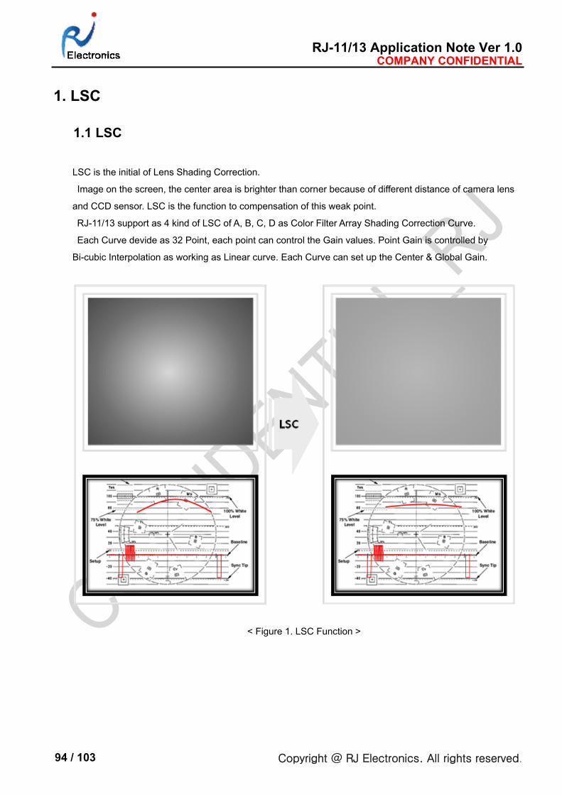
RJ-11/13 Application Note Ver 1.0 COMPANY CONFIDENTIAL
Copyright @ RJ Electronics. All rights reserved. 94 / 103
1. LSC
1.1 LSC
LSC is the initial of Lens Shading Correction.
Image on the screen, the center area is brighter than corner because of different distance of camera lens
and CCD sensor. LSC is the function to compensation of this weak point.
RJ-11/13 support as 4 kind of LSC of A, B, C, D as Color Filter Array Shading Correction Curve.
Each Curve devide as 32 Point, each point can control the Gain values. Point Gain is controlled by
Bi-cubic Interpolation as working as Linear curve. Each Curve can set up the Center & Global Gain.
< Figure 1. LSC Function >
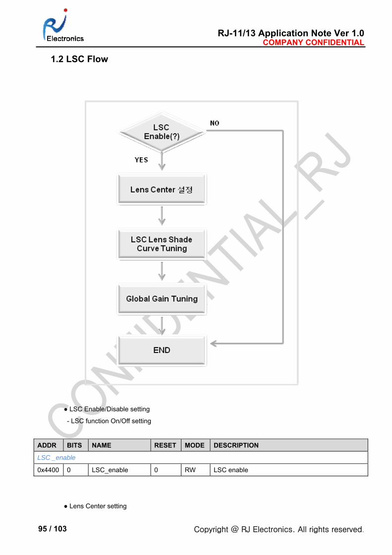
RJ-11/13 Application Note Ver 1.0 COMPANY CONFIDENTIAL
Copyright @ RJ Electronics. All rights reserved. 95 / 103
1.2 LSC Flow
● LSC Enable/Disable setting
- LSC function On/Off setting
ADDR BITS NAME RESET MODE DESCRIPTION
LSC _enable
0x4400 0 LSC_enable 0 RW LSC enable
● Lens Center setting
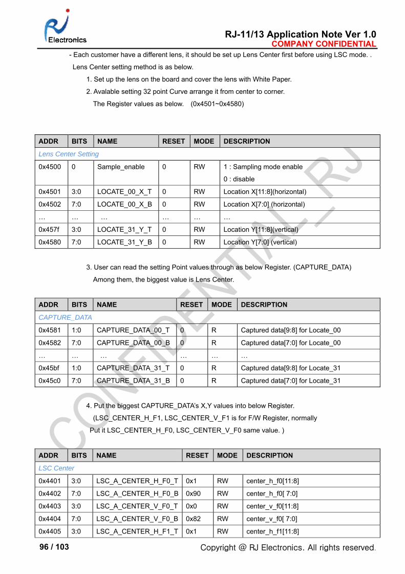
RJ-11/13 Application Note Ver 1.0 COMPANY CONFIDENTIAL
Copyright @ RJ Electronics. All rights reserved. 96 / 103
- Each customer have a different lens, it should be set up Lens Center first before using LSC mode. .
Lens Center setting method is as below.
1. Set up the lens on the board and cover the lens with White Paper.
2. Avalable setting 32 point Curve arrange it from center to corner.
The Register values as below. (0x4501~0x4580)
ADDR BITS NAME RESET MODE DESCRIPTION
Lens Center Setting
0x4500 0 Sample_enable 0 RW 1 : Sampling mode enable
0 : disable
0x4501 3:0 LOCATE_00_X_T 0 RW Location X[11:8](horizontal)
0x4502 7:0 LOCATE_00_X_B 0 RW Location X[7:0] (horizontal)
… … … … … …
0x457f 3:0 LOCATE_31_Y_T 0 RW Location Y[11:8](vertical)
0x4580 7:0 LOCATE_31_Y_B 0 RW Location Y[7:0] (vertical)
3. User can read the setting Point values through as below Register. (CAPTURE_DATA)
Among them, the biggest value is Lens Center.
ADDR BITS NAME RESET MODE DESCRIPTION
CAPTURE_DATA
0x4581 1:0 CAPTURE_DATA_00_T 0 R Captured data[9:8] for Locate_00
0x4582 7:0 CAPTURE_DATA_00_B 0 R Captured data[7:0] for Locate_00
… … … … … …
0x45bf 1:0 CAPTURE_DATA_31_T 0 R Captured data[9:8] for Locate_31
0x45c0 7:0 CAPTURE_DATA_31_B 0 R Captured data[7:0] for Locate_31
4. Put the biggest CAPTURE_DATA’s X,Y values into below Register.
(LSC_CENTER_H_F1, LSC_CENTER_V_F1 is for F/W Register, normally
Put it LSC_CENTER_H_F0, LSC_CENTER_V_F0 same value. )
ADDR BITS NAME RESET MODE DESCRIPTION
LSC Center
0x4401 3:0 LSC_A_CENTER_H_F0_T 0x1 RW center_h_f0[11:8]
0x4402 7:0 LSC_A_CENTER_H_F0_B 0x90 RW center_h_f0[ 7:0]
0x4403 3:0 LSC_A_CENTER_V_F0_T 0x0 RW center_v_f0[11:8]
0x4404 7:0 LSC_A_CENTER_V_F0_B 0x82 RW center_v_f0[ 7:0]
0x4405 3:0 LSC_A_CENTER_H_F1_T 0x1 RW center_h_f1[11:8]
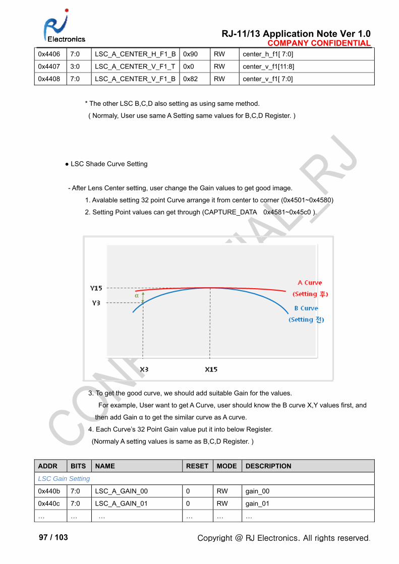
RJ-11/13 Application Note Ver 1.0 COMPANY CONFIDENTIAL
Copyright @ RJ Electronics. All rights reserved. 97 / 103
0x4406 7:0 LSC_A_CENTER_H_F1_B 0x90 RW center_h_f1[ 7:0]
0x4407 3:0 LSC_A_CENTER_V_F1_T 0x0 RW center_v_f1[11:8]
0x4408 7:0 LSC_A_CENTER_V_F1_B 0x82 RW center_v_f1[ 7:0]
* The other LSC B,C,D also setting as using same method.
( Normaly, User use same A Setting same values for B,C,D Register. )
● LSC Shade Curve Setting
- After Lens Center setting, user change the Gain values to get good image.
1. Avalable setting 32 point Curve arrange it from center to corner (0x4501~0x4580)
2. Setting Point values can get through (CAPTURE_DATA 0x4581~0x45c0 ).
3. To get the good curve, we should add suitable Gain for the values.
For example, User want to get A Curve, user should know the B curve X,Y values first, and
then add Gain α to get the similar curve as A curve.
4. Each Curve’s 32 Point Gain value put it into below Register.
(Normaly A setting values is same as B,C,D Register. )
ADDR BITS NAME RESET MODE DESCRIPTION
LSC Gain Setting
0x440b 7:0 LSC_A_GAIN_00 0 RW gain_00
0x440c 7:0 LSC_A_GAIN_01 0 RW gain_01
… … … … … …
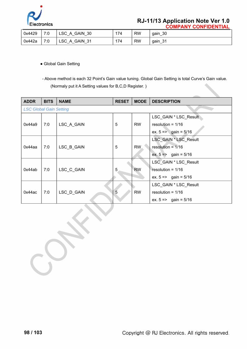
RJ-11/13 Application Note Ver 1.0 COMPANY CONFIDENTIAL
Copyright @ RJ Electronics. All rights reserved. 98 / 103
0x4429 7:0 LSC_A_GAIN_30 174 RW gain_30
0x442a 7:0 LSC_A_GAIN_31 174 RW gain_31
● Global Gain Setting
- Above method is each 32 Point’s Gain value tuning. Global Gain Setting is total Curve’s Gain value.
(Normaly put it A Setting values for B,C,D Register. )
ADDR BITS NAME RESET MODE DESCRIPTION
LSC Global Gain Setting
0x44a9 7:0 LSC_A_GAIN 5 RW
LSC_GAIN * LSC_Result
resolution = 1/16
ex. 5 => gain = 5/16
0x44aa 7:0 LSC_B_GAIN 5 RW
LSC_GAIN * LSC_Result
resolution = 1/16
ex. 5 => gain = 5/16
0x44ab 7:0 LSC_C_GAIN 5 RW
LSC_GAIN * LSC_Result
resolution = 1/16
ex. 5 => gain = 5/16
0x44ac 7:0 LSC_D_GAIN 5 RW
LSC_GAIN * LSC_Result
resolution = 1/16
ex. 5 => gain = 5/16
RJ-11/13 Application Note Ver 1.0 COMPANY CONFIDENTIAL
Copyright @ RJ Electronics. All rights reserved. 99 / 103
RJ-11/13
Defect Pixel Cancelling APPLICATION NOTE Ver 1.0
RJ-11/13
Document #: RJ11/13-A01
RJ-11/13 Application Note Ver 1.0 COMPANY CONFIDENTIAL
Copyright @ RJ Electronics. All rights reserved. 100 / 103
REVISION HISTORY
VERSION : Ver 1.0
DATE ;
Author ;
APPROVER ;
Description
ORIGINAL

RJ-11/13 Application Note Ver 1.0 COMPANY CONFIDENTIAL
Copyright @ RJ Electronics. All rights reserved. 101 / 103
This document contains information on a new product. Specifications and information herein are subject to
change without notice.
Use of this specification for product design requires an executed license agreement from RJ Electronics.
RJ Eletronics shall not be liable for technical or editorial errors or omissions contained herein; nor for incidental
or consequential damages resulting from the furnishing, performance, or use of this material. Copyright law
protects all parts of the RJ Specification and all rights are reserved. This documentation may not, in whole or in
part, be copied, photocopied, reproduced, translated, or reduced to any electronic medium or machine readable
form without prior consent, in writing, from RJ Electronics.
RJ-11/13 Application Note Ver 1.0 COMPANY CONFIDENTIAL
Copyright @ RJ Electronics. All rights reserved. 102 / 103
TABLE OF CONTENTS
INDEX REVISION HISTORY ........................................................................................................................................................ 100
TABLE OF CONTENTS .................................................................................................................................................... 102
1. Defect Pixel Cancelling ............................................................................................................................................... 103
1.1 Defect Pixel Cancelling ....................................................................................................................................... 103
1.2 Register ................................................................................................................................................................ 103
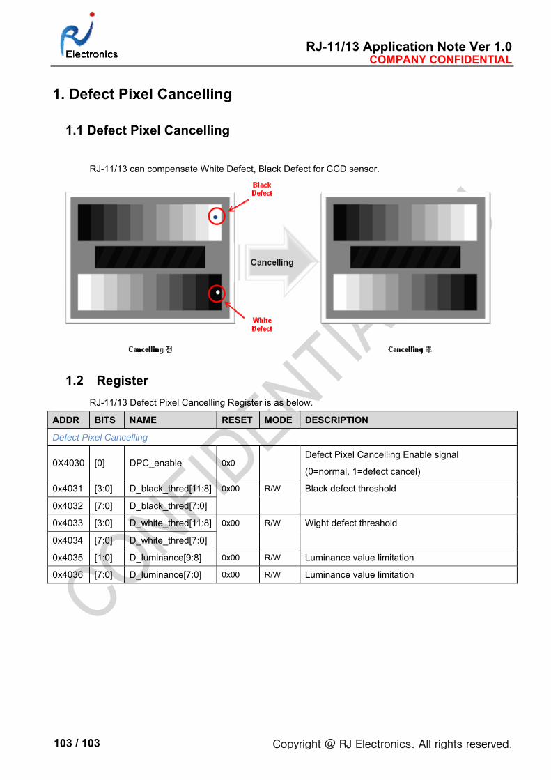
RJ-11/13 Application Note Ver 1.0 COMPANY CONFIDENTIAL
Copyright @ RJ Electronics. All rights reserved. 103 / 103
1. Defect Pixel Cancelling
1.1 Defect Pixel Cancelling
RJ-11/13 can compensate White Defect, Black Defect for CCD sensor.
1.2 Register
RJ-11/13 Defect Pixel Cancelling Register is as below.
ADDR BITS NAME RESET MODE DESCRIPTION
Defect Pixel Cancelling
0X4030 [0] DPC_enable 0x0 Defect Pixel Cancelling Enable signal
(0=normal, 1=defect cancel)
0x4031 [3:0] D_black_thred[11:8] 0x00 R/W Black defect threshold
0x4032 [7:0] D_black_thred[7:0]
0x4033 [3:0] D_white_thred[11:8] 0x00 R/W Wight defect threshold
0x4034 [7:0] D_white_thred[7:0]
0x4035 [1:0] D_luminance[9:8] 0x00 R/W Luminance value limitation
0x4036 [7:0] D_luminance[7:0] 0x00 R/W Luminance value limitation