Embed Size (px)
Citation preview
R10DS0205EJ0200 Rev.2.00 Page 1 of 13 2016.1.12
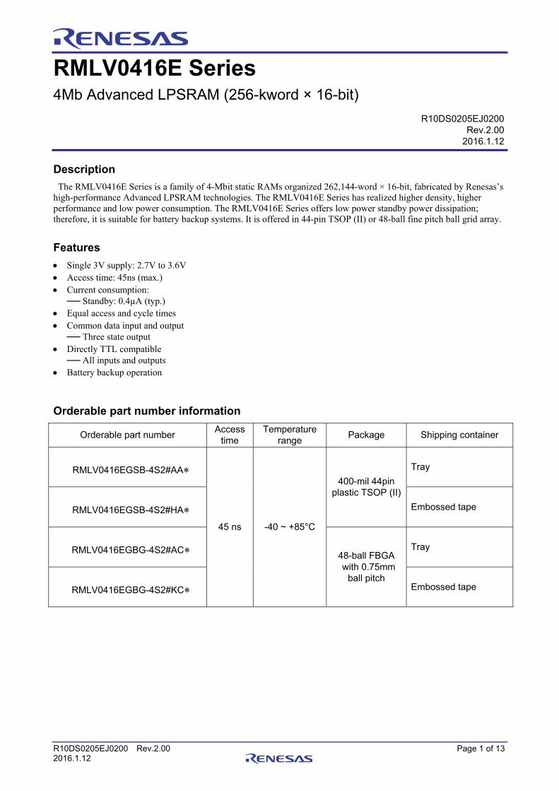
RMLV0416E Series 4Mb Advanced LPSRAM (256-kword × 16-bit)
Description
The RMLV0416E Series is a family of 4-Mbit static RAMs organized 262,144-word × 16-bit, fabricated by Renesas’s high-performance Advanced LPSRAM technologies. The RMLV0416E Series has realized higher density, higher performance and low power consumption. The RMLV0416E Series offers low power standby power dissipation; therefore, it is suitable for battery backup systems. It is offered in 44-pin TSOP (II) or 48-ball fine pitch ball grid array.
Features
Single 3V supply: 2.7V to 3.6V Access time: 45ns (max.) Current consumption:
── Standby: 0.4µA (typ.) Equal access and cycle times Common data input and output
── Three state output Directly TTL compatible
── All inputs and outputs Battery backup operation
Orderable part number information
Orderable part number Access
time Temperature
range Package Shipping container
RMLV0416EGSB-4S2#AA*
45 ns -40 ~ +85°C
400-mil 44pin plastic TSOP (II)
Tray
RMLV0416EGSB-4S2#HA* Embossed tape
RMLV0416EGBG-4S2#AC* 48-ball FBGA with 0.75mm
ball pitch
Tray
RMLV0416EGBG-4S2#KC* Embossed tape
R10DS0205EJ0200Rev.2.00
2016.1.12

RMLV0416E Series
R10DS0205EJ0200 Rev.2.00 Page 2 of 13 2016.1.12
Pin Arrangement
Pin Description
Pin name Function
VCC Power supply
VSS Ground
A0 to A17 Address input
I/O0 to I/O15 Data input/output
CS1# Chip select 1
CS2 Chip select 2
OE# Output enable
WE# Write enable
LB# Lower byte select
UB# Upper byte select
NC No connection
LB# A0 OE# A1 A2 CS2 A
I/O8 A3 UB# A4 CS1# I/O0 B
I/O9 A5 I/O10 A6 I/O1 I/O2 C
Vss A17 I/O11 A7 I/O3 Vcc D
Vcc NC I/O12 A16 I/O4 Vss E
I/O14 A14 I/O13 A15 I/O5 I/O6 F
I/O15 A12 NC A13 WE# I/O7 G
NC A9 A8 A10 A11 NC H
1 3 2 4 5 6
(Top view)
48-ball FBGA
A4
A3
A2
A1
A0
CS1#
I/O0
I/O1
I/O2
I/O3
Vcc
Vss
I/O4
I/O5
I/O6
I/O7
WE#
A17
A16
A15
A14
A13
A5
A6
A7
OE#
UB#
LB#
I/O15
I/O14
I/O13
I/O12
Vss
Vcc
I/O11
I/O10
I/O9
I/O8
CS2
A8
A9
A10
A11
A12
1
2
3
4
5
6
7
8
9
10
11
12
13
14
15
16
17
18
19
20
21
22
44
43
42
41
40
39
38
37
36
35
34
33
32
31
30
29
28
27
26
25
24
23
(Top view)
44pin TSOP (II)
RMLV0416E Series
R10DS0205EJ0200 Rev.2.00 Page 3 of 13 2016.1.12
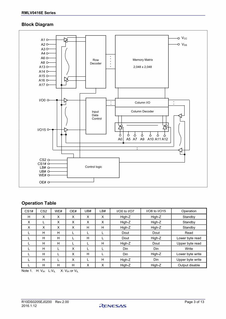
Block Diagram
Operation Table
CS1# CS2 WE# OE# UB# LB# I/O0 to I/O7 I/O8 to I/O15 Operation
H X X X X X High-Z High-Z Standby
X L X X X X High-Z High-Z Standby
X X X X H H High-Z High-Z Standby
L H H L L L Dout Dout Read
L H H L H L Dout High-Z Lower byte read
L H H L L H High-Z Dout Upper byte read
L H L X L L Din Din Write
L H L X H L Din High-Z Lower byte write
L H L X L H High-Z Din Upper byte write
L H H H X X High-Z High-Z Output disable
Note 1. H: VIH L:VIL X: VIH or VIL
Memory Matrix
A1A2A3A4A6A8
A13A14A15A16A17
2,048 x 2,048
Row Decoder
・・・・・
Input Data Control
A12A11 A10 A9 A7 A5 A0
・・ ・・
・・
I/O0
I/O15
CS2CS1#
OE#
VCC
VSS
Control logic
Column I/O
Column Decoder
LB#UB#WE#

RMLV0416E Series
R10DS0205EJ0200 Rev.2.00 Page 4 of 13 2016.1.12
Absolute Maximum Ratings
Parameter Symbol Value unit
Power supply voltage relative to VSS VCC -0.5 to +4.6 V
Terminal voltage on any pin relative to VSS VT -0.5*2 to VCC+0.3*3 V
Power dissipation PT 0.7 W
Operation temperature Topr -40 to +85 °C
Storage temperature range Tstg -65 to +150 °C
Storage temperature range under bias Tbias -40 to +85 °C
Note 2. -3.0V for pulse ≤ 30ns (full width at half maximum)
3. Maximum voltage is +4.6V.
DC Operating Conditions
Parameter Symbol Min. Typ. Max. Unit Note
Supply voltage VCC 2.7 3.0 3.6 V
VSS 0 0 0 V
Input high voltage VIH 2.2 ─ VCC+0.3 V
Input low voltage VIL -0.3 ─ 0.6 V 4
Ambient temperature range Ta -40 ─ +85 °C
Note 4. -3.0V for pulse ≤ 30ns (full width at half maximum)
DC Characteristics
Parameter Symbol Min. Typ. Max. Unit Test conditions
Input leakage current | ILI | ─ ─ 1 A Vin = VSS to VCC
Output leakage current
| ILO | ─ ─ 1 A CS1# = VIH or CS2 = VIL or OE# = VIH
or WE# = VIL or LB# = UB# = VIH, VI/O = VSS to VCC
Operating current ICC ─ ─ 10 mA
CS1# = VIL, CS2 = VIH, Others = VIH/VIL,
II/O = 0mA
Average operating current
ICC1
─ ─ 20 mA Cycle = 55ns, duty =100%, II/O = 0mA,
CS1# = VIL, CS2 = VIH, Others = VIH/VIL
─ ─ 25 mA Cycle = 45ns, duty =100%, II/O = 0mA,
CS1# = VIL, CS2 = VIH, Others = VIH/VIL
ICC2 ─ ─ 2.5 mA
Cycle =1s, duty =100%, II/O = 0mA,
CS1# ≤ 0.2V, CS2 ≥ VCC-0.2V,
VIH ≥ VCC-0.2V, VIL ≤ 0.2V
Standby current ISB ─ 0.1*5 0.3 mA CS2 = VIL, Others = VSS to VCC
Standby current
ISB1
─ 0.4*5 2 A ~+25°C Vin = VSS to VCC,
(1) CS2 ≤ 0.2V or
(2) CS1# ≥ VCC-0.2V,
CS2 ≥ VCC-0.2V or
(3) LB# = UB# ≥ VCC-0.2V,
CS1# ≤ 0.2V, CS2 ≥ VCC-0.2V
─ ─ 3 A ~+40°C
─ ─ 5 A ~+70°C
─ ─ 7 A ~+85°C
Output high voltage VOH 2.4 ─ ─ V IOH = -1mA
VOH2 VCC-0.2 ─ ─ V IOH = -0.1mA
Output low voltage VOL ─ ─ 0.4 V IOL = 2mA
VOL2 ─ ─ 0.2 V IOL = 0.1mA
Note 5. Typical parameter indicates the value for the center of distribution at 3.0V (Ta=25ºC), and not 100% tested.
Capacitance
(Vcc = 2.7V ~ 3.6V, f = 1MHz, Ta = -40 ~ +85°C)
Parameter Symbol Min. Typ. Max. Unit Test conditions Note
Input capacitance C in ─ ─ 8 pF Vin =0V 6
Input / output capacitance C I/O ─ ─ 10 pF VI/O =0V 6
Note 6. This parameter is sampled and not 100% tested.

RMLV0416E Series
R10DS0205EJ0200 Rev.2.00 Page 5 of 13 2016.1.12
AC Characteristics
Test Conditions (Vcc = 2.7V ~ 3.6V, Ta = -40 ~ +85°C)
Input pulse levels: VIL = 0.4V, VIH = 2.4V Input rise and fall time: 5ns Input and output timing reference level: 1.4V Output load: See figures (Including scope and jig)
Read Cycle
Parameter Symbol Min. Max. Unit Note
Read cycle time tRC 45 ns
Address access time tAA ─ 45 ns
Chip select access time tACS1 ─ 45 ns
tACS2 ─ 45 ns
Output enable to output valid tOE ─ 22 ns
Output hold from address change tOH 10 ─ ns
LB#, UB# access time tBA ─ 45 ns
Chip select to output in low-Z tCLZ1 10 ─ ns 7,8
tCLZ2 10 ─ ns 7,8
LB#, UB# enable to low-Z tBLZ 5 ─ ns 7,8
Output enable to output in low-Z tOLZ 5 ─ ns 7,8
Chip deselect to output in high-Z tCHZ1 0 18 ns 7,8,9
tCHZ2 0 18 ns 7,8,9
LB#, UB# disable to high-Z tBHZ 0 18 ns 7,8,9
Output disable to output in high-Z tOHZ 0 18 ns 7,8,9
Note 7. This parameter is sampled and not 100% tested.
8. At any given temperature and voltage condition, tCHZ1 max is less than tCLZ1 min, tCHZ2 max is less than tCLZ2 min, tBHZ max is less than tBLZ min, and tOHZ max is less than tOLZ min, for any device.
9. tCHZ1, tCHZ2, tBHZ and tOHZ are defined as the time when the I/O pins enter a high-impedance state and are not referred to the I/O levels.
I/O
1.4V
RL = 500 ohm
CL = 30 pF

RMLV0416E Series
R10DS0205EJ0200 Rev.2.00 Page 6 of 13 2016.1.12
Write Cycle
Parameter Symbol Min. Max. Unit Note
Write cycle time tWC 45 ─ ns
Address valid to write end tAW 35 ─ ns
Chip select to write end tCW 35 ─ ns
Write pulse width tWP 35 ─ ns 10
LB#,UB# valid to write end tBW 35 ─ ns
Address setup time to write start tAS 0 ─ ns
Write recovery time from write end tWR 0 ─ ns
Data to write time overlap tDW 25 ─ ns
Data hold from write end tDH 0 ─ ns
Output enable from write end tOW 5 ─ ns 11
Output disable to output in high-Z tOHZ 0 18 ns 11,12
Write to output in high-Z tWHZ 0 18 ns 11,12
Note 10. tWP is the interval between write start and write end.
A write starts when all of (CS1#), (CS2), (WE#) and (one or both of LB# and UB#) become active.
A write is performed during the overlap of a low CS1#, a high CS2, a low WE# and a low LB# or a low UB#.
A write ends when any of (CS1#), (CS2), (WE#) or (one or both of LB# and UB#) becomes inactive.
11. This parameter is sampled and not 100% tested.
12. tOHZ and tWHZ are defined as the time when the I/O pins enter a high-impedance state and are not referred to the I/O levels.

RMLV0416E Series
R10DS0205EJ0200 Rev.2.00 Page 7 of 13 2016.1.12
Timing Waveforms
Read Cycle
Note 13. tCHZ1, tCHZ2, tBHZ and tOHZ are defined as the time when the I/O pins enter a high-impedance state and are not referred to the I/O levels.
14. This parameter is sampled and not 100% tested
15. At any given temperature and voltage condition, tCHZ1 max is less than tCLZ1 min, tCHZ2 max is less than tCLZ2 min, tBHZ max is less than tBLZ min, and tOHZ max is less than tOLZ min, for any device.
tAA
CS1#
A0~17
tOH
tCLZ1
tACS1
tOE
tOLZ
tCHZ1
OE#
WE#
I/O0~15
VIH
tOHZ
WE# = “H” level
tRC
tBLZ tBHZ
LB#,UB#
tBA
CS2 tACS2
tCLZ2 tCHZ2
High impedance Valid Data
*14,15
*14,15
*14,15
*14,15
*13,14,15
*13,14,15
*13,14,15
*13,14,15
Valid address

RMLV0416E Series
R10DS0205EJ0200 Rev.2.00 Page 8 of 13 2016.1.12
Write Cycle (1) (WE# CLOCK, OE#=”H” while writing)
Note 16. tWP is the minimum time to perform a write.
A write starts when all of (CS1#), (CS2), (WE#) and (one or both of LB# and UB#) become active.
A write is performed during the overlap of a low CS1#, a high CS2, a low WE# and a low LB# or a low UB#.
A write ends when any of (CS1#), (CS2), (WE#) or (one or both of LB# and UB#) becomes inactive.
17. tOHZ and tWHZ are defined as the time when the I/O pins enter a high-impedance state and are not referred to the I/O levels.
18. This parameter is sampled and not 100% tested
19. During this period, I/O pins are in the output state so input signals must not be applied to the I/O pins.
CS1#
A0~17
tCW
tWHZ OE#
WE#
I/O0~15
tDH
tWC
LB#,UB#
tBW
CS2 tCW
Valid address
tWR tAW
tAS
tWP
tDW
*16
*17,18
*17,18 tOHZ
Valid Data *19

RMLV0416E Series
R10DS0205EJ0200 Rev.2.00 Page 9 of 13 2016.1.12
Write Cycle (2) (WE# CLOCK, OE# Low Fixed)
Note 20. tWP is the minimum time to perform a write.
A write starts when all of (CS1#), (CS2), (WE#) and (one or both of LB# and UB#) become active.
A write is performed during the overlap of a low CS1#, a high CS2, a low WE# and a low LB# or a low UB#.
A write ends when any of (CS1#), (CS2), (WE#) or (one or both of LB# and UB#) becomes inactive.
21. tWHZ is defined as the time when the I/O pins enter a high-impedance state and are not referred to the I/O levels.
22. This parameter is sampled and not 100% tested.
23. During this period, I/O pins are in the output state so input signals must not be applied to the I/O pins.
CS1#
A0~17
tCW
tWHZ
OE#
WE#
I/O0~15
tDH
tWC
LB#,UB#
tBW
CS2 tCW
Valid address
tWR tAW
tAS
tWP
tDW
tOW
*20
*21,22
VIL OE# = “L” level
Valid Data *23 *23

RMLV0416E Series
R10DS0205EJ0200 Rev.2.00 Page 10 of 13 2016.1.12
Write Cycle (3) (CS1#, CS2 CLOCK)
Note 24. tWP is the minimum time to perform a write.
A write starts when all of (CS1#), (CS2), (WE#) and (one or both of LB# and UB#) become active.
A write is performed during the overlap of a low CS1#, a high CS2, a low WE# and a low LB# or a low UB#.
A write ends when any of (CS1#), (CS2), (WE#) or (one or both of LB# and UB#) becomes inactive.
CS1#
A0~17
tCW
OE#
WE#
I/O0~15
tDH
tWC
LB#,UB#
tBW
CS2
Valid address
tWR
tAW
tAS
tWP
tDW
VIH OE# = “H” level
tCW tAS
*24
Valid Data Valid Data

RMLV0416E Series
R10DS0205EJ0200 Rev.2.00 Page 11 of 13 2016.1.12
Write Cycle (4) (LB#, UB# CLOCK)
Note 25. tWP is the minimum time to perform a write.
A write starts when all of (CS1#), (CS2), (WE#) and (one or both of LB# and UB#) become active.
A write is performed during the overlap of a low CS1#, a high CS2, a low WE# and a low LB# or a low UB#.
A write ends when any of (CS1#), (CS2), (WE#) or (one or both of LB# and UB#) becomes inactive.
CS1#
A0~17
tCW
OE#
WE#
I/O0~15
tDH
tWC
LB#,UB#
tBW
CS2
Valid address
tWR
tAW
tAS
tWP
tDW
VIH OE# = “H” level
tCW
*25
Valid Data

RMLV0416E Series
R10DS0205EJ0200 Rev.2.00 Page 12 of 13 2016.1.12
Low VCC Data Retention Characteristics
Parameter Symbol Min. Typ. Max. Unit Test conditions*27
VCC for data retention VDR 1.5 ─ ─ V
Vin ≥ 0V,
(1) CS2 ≤ 0.2V
or
(2) CS1# ≥ VCC-0.2V, CS2 ≥ VCC-0.2V
or
(3) LB# = UB# ≥ VCC-0.2V,
CS1# ≤ 0.2V, CS2 ≥ VCC-0.2V
Data retention current ICCDR
─ 0.4*26 2 A ~+25°C VCC = 3.0V, Vin ≥ 0V,
(1) CS2 ≤ 0.2V
or
(2) CS1# ≥ VCC-0.2V, CS2 ≥ VCC-0.2V
or
(3) LB# = UB# ≥ VCC-0.2V,
CS1# ≤ 0.2V,
CS2 ≥ VCC-0.2V
─ ─ 3 A ~+40°C
─ ─ 5 A ~+70°C
─ ─ 7 A ~+85°C
Chip deselect time to data retention tCDR 0 ─ ─ ns See retention waveform.
Operation recovery time tR 5 ─ ─ ms
Note 26. Typical parameter indicates the value for the center of distribution at 3.0V (Ta=25ºC), and not 100% tested.
27. CS2 controls address buffer, WE# buffer, CS1# buffer, OE# buffer, LB# buffer, UB# buffer and I/O buffer. If CS2 controls data retention mode, Vin levels (address, WE#, CS1#, OE#, LB#, UB#, I/O) can be in the high impedance state. If CS1# controls data retention mode, CS2 must be CS2 ≥ VCC-0.2V or CS2 ≤ 0.2V. The other inputs levels (address, WE#, OE#, LB#, UB#, I/O) can be in the high-impedance state.

RMLV0416E Series
R10DS0205EJ0200 Rev.2.00 Page 13 of 13 2016.1.12
Low Vcc Data Retention Timing Waveforms (CS1# controlled)
Low Vcc Data Retention Timing Waveforms (CS2 controlled)
Low Vcc Data Retention Timing Waveforms (LB#,UB# controlled)
LB#,UB#
VCC
LB#,UB# Controlled
tCDR tR 2.7V 2.7V
2.2V 2.2V VDR
LB#,UB# ≥ VCC - 0.2V
CS1#
VCC
CS1# Controlled
tCDR tR 2.7V 2.7V
2.2V 2.2V VDR
CS1# ≥ VCC - 0.2V
CS2
VCC
CS2 Controlled
tCDR tR 2.7V 2.7V
0.6V 0.6V VDR
CS2 ≤ 0.2V

All trademarks and registered trademarks are the property of their respective owners.
Revision History RMLV0416E Series Data Sheet
Rev. Date
Description
Page Summary
1.00 2014.2.27 ─ First edition issued
2.00 2016.1.12 1 Changed section from “Part Name Information” to “Orderable part number information”

Notice1. Descriptions of circuits, software and other related information in this document are provided only to illustrate the operation of semiconductor products and application examples. You are fully responsible for
the incorporation of these circuits, software, and information in the design of your equipment. Renesas Electronics assumes no responsibility for any losses incurred by you or third parties arising from the
use of these circuits, software, or information.
2. Renesas Electronics has used reasonable care in preparing the information included in this document, but Renesas Electronics does not warrant that such information is error free. Renesas Electronics
assumes no liability whatsoever for any damages incurred by you resulting from errors in or omissions from the information included herein.
3. Renesas Electronics does not assume any liability for infringement of patents, copyrights, or other intellectual property rights of third parties by or arising from the use of Renesas Electronics products or
technical information described in this document. No license, express, implied or otherwise, is granted hereby under any patents, copyrights or other intellectual property rights of Renesas Electronics or
others.
4. You should not alter, modify, copy, or otherwise misappropriate any Renesas Electronics product, whether in whole or in part. Renesas Electronics assumes no responsibility for any losses incurred by you or
third parties arising from such alteration, modification, copy or otherwise misappropriation of Renesas Electronics product.
5. Renesas Electronics products are classified according to the following two quality grades: "Standard" and "High Quality". The recommended applications for each Renesas Electronics product depends on
the product's quality grade, as indicated below.
"Standard": Computers; office equipment; communications equipment; test and measurement equipment; audio and visual equipment; home electronic appliances; machine tools; personal electronic
equipment; and industrial robots etc.
"High Quality": Transportation equipment (automobiles, trains, ships, etc.); traffic control systems; anti-disaster systems; anti-crime systems; and safety equipment etc.
Renesas Electronics products are neither intended nor authorized for use in products or systems that may pose a direct threat to human life or bodily injury (artificial life support devices or systems, surgical
implantations etc.), or may cause serious property damages (nuclear reactor control systems, military equipment etc.). You must check the quality grade of each Renesas Electronics product before using it
in a particular application. You may not use any Renesas Electronics product for any application for which it is not intended. Renesas Electronics shall not be in any way liable for any damages or losses
incurred by you or third parties arising from the use of any Renesas Electronics product for which the product is not intended by Renesas Electronics.
6. You should use the Renesas Electronics products described in this document within the range specified by Renesas Electronics, especially with respect to the maximum rating, operating supply voltage
range, movement power voltage range, heat radiation characteristics, installation and other product characteristics. Renesas Electronics shall have no liability for malfunctions or damages arising out of the
use of Renesas Electronics products beyond such specified ranges.
7. Although Renesas Electronics endeavors to improve the quality and reliability of its products, semiconductor products have specific characteristics such as the occurrence of failure at a certain rate and
malfunctions under certain use conditions. Further, Renesas Electronics products are not subject to radiation resistance design. Please be sure to implement safety measures to guard them against the
possibility of physical injury, and injury or damage caused by fire in the event of the failure of a Renesas Electronics product, such as safety design for hardware and software including but not limited to
redundancy, fire control and malfunction prevention, appropriate treatment for aging degradation or any other appropriate measures. Because the evaluation of microcomputer software alone is very difficult,
please evaluate the safety of the final products or systems manufactured by you.
8. Please contact a Renesas Electronics sales office for details as to environmental matters such as the environmental compatibility of each Renesas Electronics product. Please use Renesas Electronics
products in compliance with all applicable laws and regulations that regulate the inclusion or use of controlled substances, including without limitation, the EU RoHS Directive. Renesas Electronics assumes
no liability for damages or losses occurring as a result of your noncompliance with applicable laws and regulations.
9. Renesas Electronics products and technology may not be used for or incorporated into any products or systems whose manufacture, use, or sale is prohibited under any applicable domestic or foreign laws or
regulations. You should not use Renesas Electronics products or technology described in this document for any purpose relating to military applications or use by the military, including but not limited to the
development of weapons of mass destruction. When exporting the Renesas Electronics products or technology described in this document, you should comply with the applicable export control laws and
regulations and follow the procedures required by such laws and regulations.
10. It is the responsibility of the buyer or distributor of Renesas Electronics products, who distributes, disposes of, or otherwise places the product with a third party, to notify such third party in advance of the
contents and conditions set forth in this document, Renesas Electronics assumes no responsibility for any losses incurred by you or third parties as a result of unauthorized use of Renesas Electronics
products.
11. This document may not be reproduced or duplicated in any form, in whole or in part, without prior written consent of Renesas Electronics.
12. Please contact a Renesas Electronics sales office if you have any questions regarding the information contained in this document or Renesas Electronics products, or if you have any other inquiries.
(Note 1) "Renesas Electronics" as used in this document means Renesas Electronics Corporation and also includes its majority-owned subsidiaries.
(Note 2) "Renesas Electronics product(s)" means any product developed or manufactured by or for Renesas Electronics.
http://www.renesas.comRefer to "http://www.renesas.com/" for the latest and detailed information.
Renesas Electronics America Inc.2801 Scott Boulevard Santa Clara, CA 95050-2549, U.S.A.Tel: +1-408-588-6000, Fax: +1-408-588-6130Renesas Electronics Canada Limited9251 Yonge Street, Suite 8309 Richmond Hill, Ontario Canada L4C 9T3Tel: +1-905-237-2004Renesas Electronics Europe LimitedDukes Meadow, Millboard Road, Bourne End, Buckinghamshire, SL8 5FH, U.KTel: +44-1628-585-100, Fax: +44-1628-585-900Renesas Electronics Europe GmbHArcadiastrasse 10, 40472 Düsseldorf, Germany Tel: +49-211-6503-0, Fax: +49-211-6503-1327Renesas Electronics (China) Co., Ltd.Room 1709, Quantum Plaza, No.27 ZhiChunLu Haidian District, Beijing 100191, P.R.ChinaTel: +86-10-8235-1155, Fax: +86-10-8235-7679Renesas Electronics (Shanghai) Co., Ltd.Unit 301, Tower A, Central Towers, 555 Langao Road, Putuo District, Shanghai, P. R. China 200333 Tel: +86-21-2226-0888, Fax: +86-21-2226-0999Renesas Electronics Hong Kong LimitedUnit 1601-1611, 16/F., Tower 2, Grand Century Place, 193 Prince Edward Road West, Mongkok, Kowloon, Hong KongTel: +852-2265-6688, Fax: +852 2886-9022Renesas Electronics Taiwan Co., Ltd.13F, No. 363, Fu Shing North Road, Taipei 10543, TaiwanTel: +886-2-8175-9600, Fax: +886 2-8175-9670Renesas Electronics Singapore Pte. Ltd.80 Bendemeer Road, Unit #06-02 Hyflux Innovation Centre, Singapore 339949Tel: +65-6213-0200, Fax: +65-6213-0300Renesas Electronics Malaysia Sdn.Bhd.Unit 1207, Block B, Menara Amcorp, Amcorp Trade Centre, No. 18, Jln Persiaran Barat, 46050 Petaling Jaya, Selangor Darul Ehsan, MalaysiaTel: +60-3-7955-9390, Fax: +60-3-7955-9510Renesas Electronics India Pvt. Ltd.No.777C, 100 Feet Road, HAL II Stage, Indiranagar, Bangalore, IndiaTel: +91-80-67208700, Fax: +91-80-67208777Renesas Electronics Korea Co., Ltd.12F., 234 Teheran-ro, Gangnam-Gu, Seoul, 135-080, KoreaTel: +82-2-558-3737, Fax: +82-2-558-5141
SALES OFFICES
© 2016 Renesas Electronics Corporation. All rights reserved.Colophon 5.0