Embed Size (px)
Citation preview
Role of Holistic Lithography and its
Business Opportunity
Christophe Fouquet Executive Vice President, Applications 31 October 2016
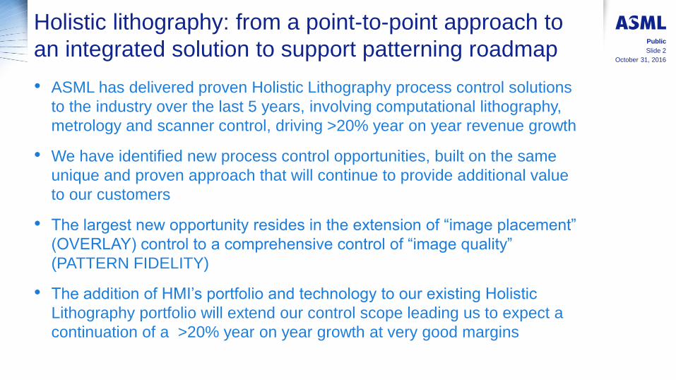
Holistic lithography: from a point-to-point approach to
an integrated solution to support patterning roadmap
• ASML has delivered proven Holistic Lithography process control solutions
to the industry over the last 5 years, involving computational lithography,
metrology and scanner control, driving >20% year on year revenue growth
• We have identified new process control opportunities, built on the same
unique and proven approach that will continue to provide additional value
to our customers
• The largest new opportunity resides in the extension of “image placement”
(OVERLAY) control to a comprehensive control of “image quality”
(PATTERN FIDELITY)
• The addition of HMI’s portfolio and technology to our existing Holistic
Lithography portfolio will extend our control scope leading us to expect a
continuation of a >20% year on year growth at very good margins
October 31, 2016
Public
Slide 2
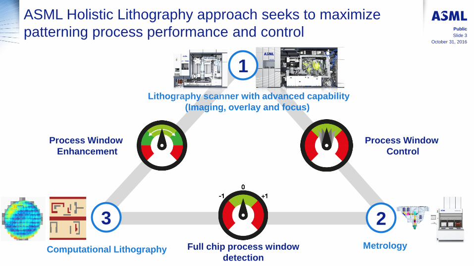
ASML Holistic Lithography approach seeks to maximize
patterning process performance and control
Full chip process window
detection
Process Window
Enhancement
Process Window
Control
Lithography scanner with advanced capability
(Imaging, overlay and focus)
Computational Lithography Metrology
1
3 2
October 31, 2016
Public
Slide 3
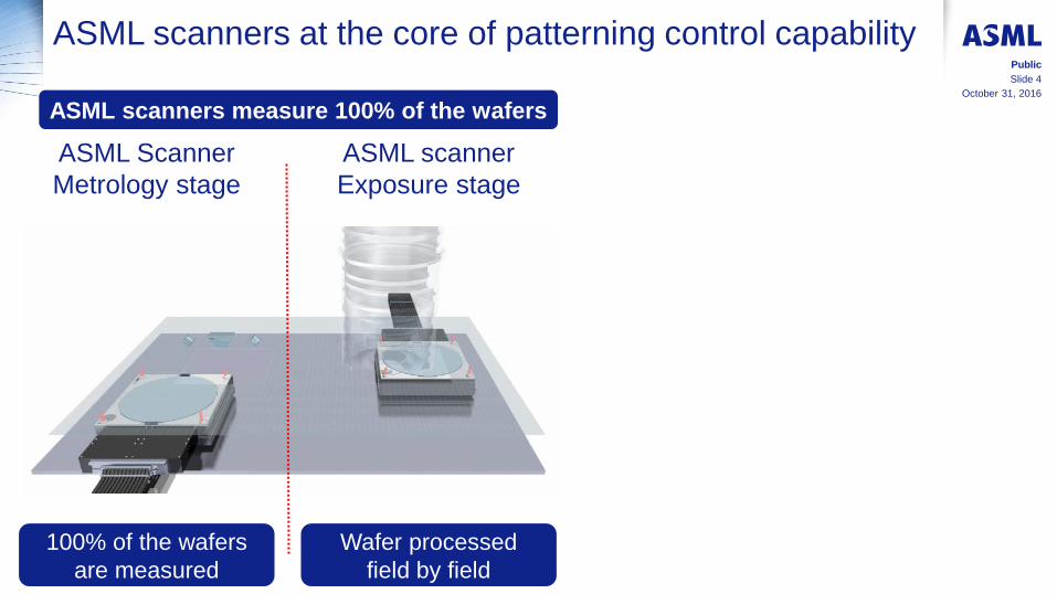
ASML scanners at the core of patterning control capability
Even Fingers
Odd Fingers
Grey Filter
X
Y
Z
Optical Centerline
Dose
manipulator
D
F
L
O
Dose
Overlay
Focus
Sca
nn
er
kn
ob
s
Wafer stage
Reticle stage
Lens
I Illumination FlexRay illuminator
ASML scanner
Exposure stage
ASML Scanner
Metrology stage
100% of the wafers
are measured
Wafer processed
field by field
ASML scanners measure 100% of the wafers ASML scanners knobs control every die
Public
Slide 4
October 31, 2016
Metrology and models are needed to describe process
fingerprint
10 nm
99.7%x: 0.9 nmy: 0.7 nm
XYSMO_DCOSAT1_20140406_0305 (S2F)
NXE:3300
Champion data
(0.9-0.7 nm)
Scanner OVERLAY < 2 nm What is the real overlay on customer products?
Wafer 1 Wafer 2
<100pts/ wafer <100pts/ wafer
Wafer A # points = 100
15 nm
99.7%x: 12.0 nmy: 10.4 nm
Wafer B # points = 100
15 nm
99.7%x: 25.0 nmy: 13.0 nm
<200pts/ wafer <200pts/ wafer
Wafer A # points = 200
15 nm
99.7%x: 11.3 nmy: 10.4 nm
Wafer B # points = 200
15 nm
99.7%x: 11.6 nmy: 12.2 nm
<300pts/ wafer <300pts/ wafer
Maximum allocated metrology cost
Wafer A # points = 300
15 nm
99.7%x: 12.0 nmy: 11.3 nm
Wafer B # points = 300
15 nm
99.7%x: 14.0 nmy: 12.2 nm
Wafer A # points = 1677
15 nm
99.7%x: 11.9 nmy: 11.3 nm
Wafer B # points = 1677
15 nm
99.7%x: 11.0 nmy: 13.2 nm
>1500pts/ wafer >1500pts/ wafer
+ Use of computational lithography
October 31, 2016
Public
Slide 5
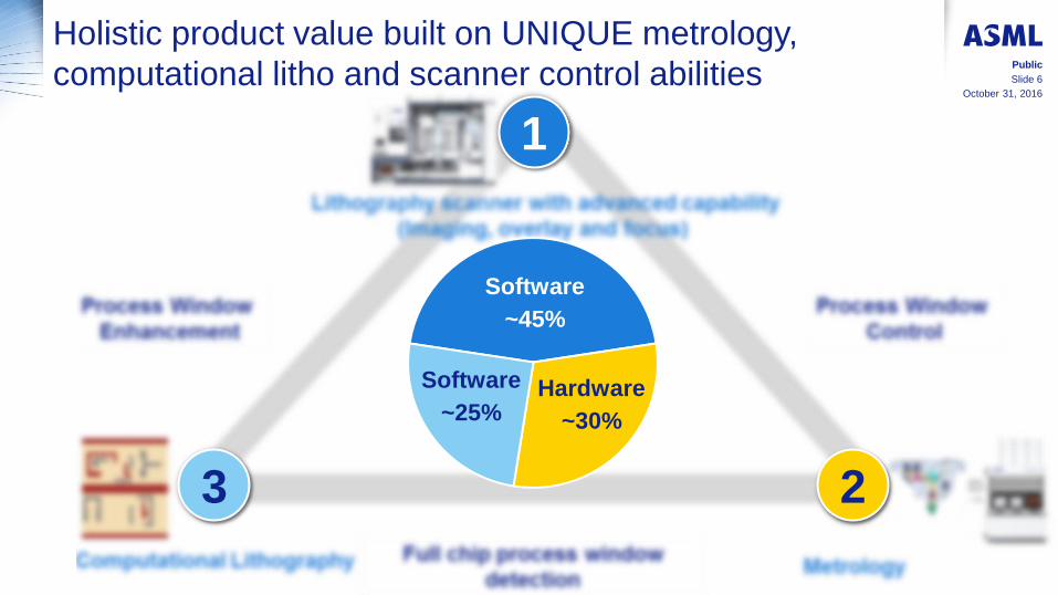
Holistic product value built on UNIQUE metrology,
computational litho and scanner control abilities
Software
~45%
Hardware
~30%
Software
~25%
2 3
1 October 31, 2016
Public
Slide 6
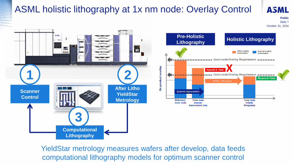
ASML holistic lithography at 1x nm node: Overlay Control
YieldStar metrology measures wafers after develop, data feeds
computational lithography models for optimum scanner control
Computational
Lithography
After Litho
YieldStar
Metrology
Scanner
Control
1
3
2
Pre-Holistic
Lithography Holistic Lithography
October 31, 2016
Public
Slide 7
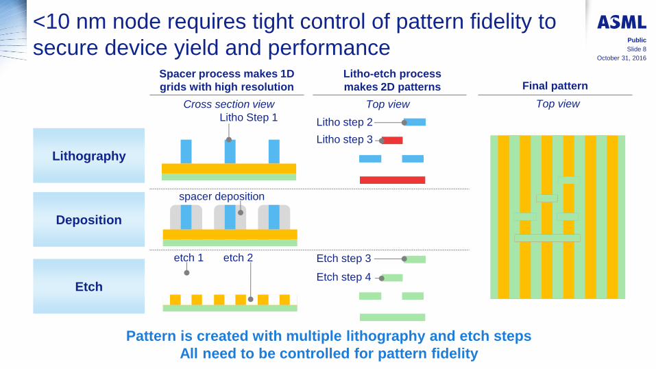
<10 nm node requires tight control of pattern fidelity to
secure device yield and performance October 31, 2016
Public
Slide 8
Top view
Lithography
Deposition
Etch
Cross section view
Spacer process makes 1D
grids with high resolution
Top view
Litho-etch process
makes 2D patterns Final pattern
Litho Step 1
spacer deposition
etch 1 etch 2 strip
Litho step 2
Litho step 3
Etch step 3
Etch step 4
Pattern is created with multiple lithography and etch steps
All need to be controlled for pattern fidelity
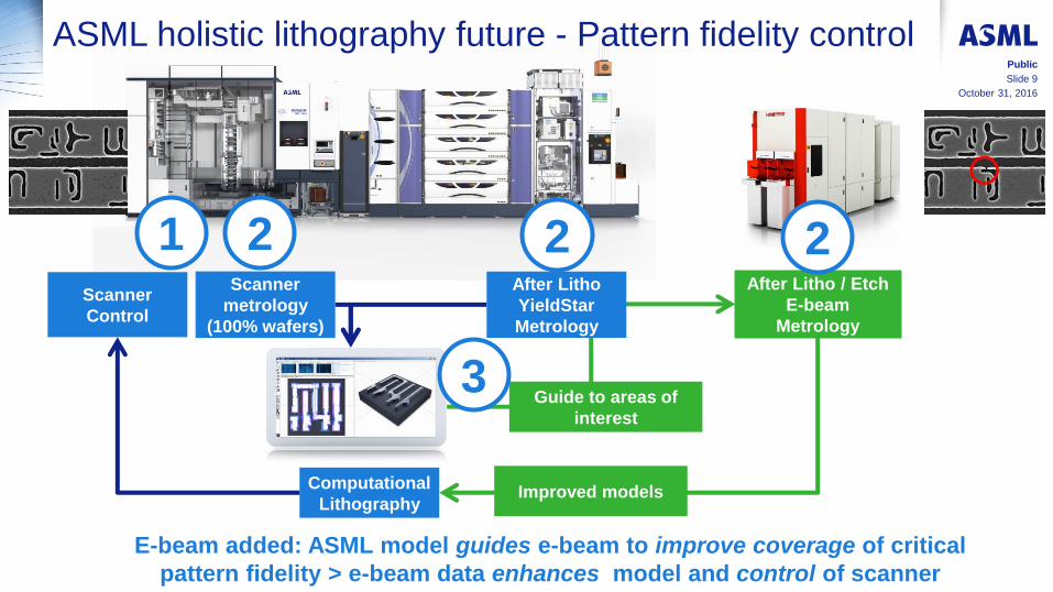
ASML holistic lithography future - Pattern fidelity control
E-beam added: ASML model guides e-beam to improve coverage of critical
pattern fidelity > e-beam data enhances model and control of scanner
Computational
Lithography
Scanner
Control
1 2 After Litho / Etch
E-beam
Metrology
Guide to areas of
interest
2 2 Scanner
metrology
(100% wafers)
Improved models
October 31, 2016
Public
Slide 9
3
After Litho
YieldStar
Metrology
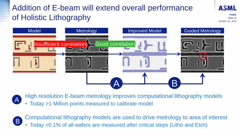
Addition of E-beam will extend overall performance
of Holistic Lithography
A
A High resolution E-beam metrology improves computational lithography models
• Today >1 Million points measured to calibrate model
B
B
Computational lithography models are used to drive metrology to area of interest
• Today <0.1% of all wafers are measured after critical steps (Litho and Etch)
Model Metrology Improved Model Guided Metrology
October 31, 2016
Public
Slide 10
Insufficient correlation Good correlation
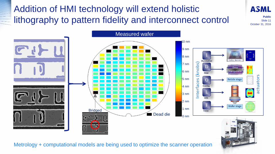
Addition of HMI technology will extend holistic
lithography to pattern fidelity and interconnect control
Metrology + computational models are being used to optimize the scanner operation
Corrected wafer Measured wafer
10 nm
9 nm
8 nm
7 nm
6 nm
5 nm
4 nm
3 nm
2 nm
1 nm
0 nm
Bridged Dead die
October 31, 2016
Public
Slide 11
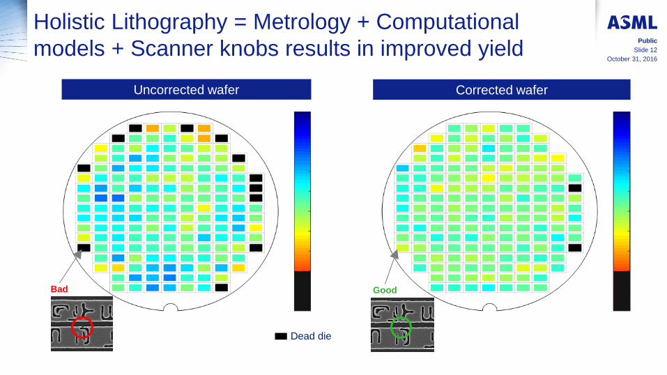
Holistic Lithography = Metrology + Computational
models + Scanner knobs results in improved yield
Uncorrected wafer
Good
Corrected wafer
Dead die
Bad
October 31, 2016
Public
Slide 12
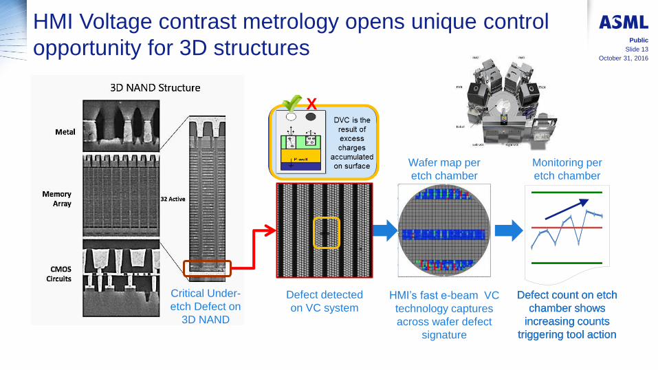
HMI Voltage contrast metrology opens unique control
opportunity for 3D structures
Defect count on etch
chamber shows
increasing counts
triggering tool action
Critical Under-
etch Defect on
3D NAND
Defect detected
on VC system HMI’s fast e-beam VC
technology captures
across wafer defect
signature
Wafer map per
etch chamber
Defect count on etch
chamber shows
increasing counts
triggering tool action
Monitoring per
etch chamber
X
October 31, 2016
Public
Slide 13
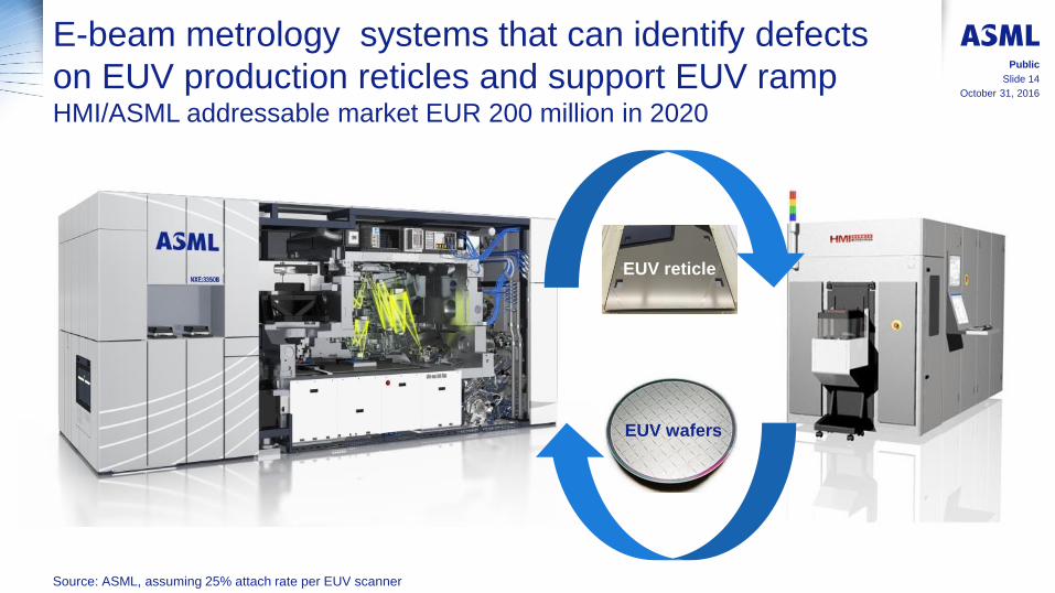
E-beam metrology systems that can identify defects
on EUV production reticles and support EUV ramp HMI/ASML addressable market EUR 200 million in 2020
EUV wafers
EUV reticle
Source: ASML, assuming 25% attach rate per EUV scanner
October 31, 2016
Public
Slide 14
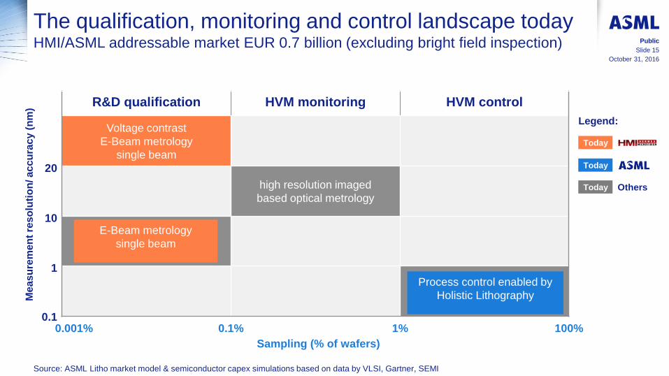
The qualification, monitoring and control landscape today HMI/ASML addressable market EUR 0.7 billion (excluding bright field inspection)
R&D qualification HVM monitoring HVM control
Voltage contrast
E-Beam metrology
single beam
high resolution imaged
based optical metrology
Me
as
ure
me
nt
res
olu
tio
n/ a
cc
ura
cy (
nm
)
10
20
0.1
1
0.001% 0.1% 1%
Sampling (% of wafers)
Source: ASML Litho market model & semiconductor capex simulations based on data by VLSI, Gartner, SEMI
100%
Today
Today
Today Others
Legend:
October 31, 2016
Public
Slide 15
Process control enabled by
Holistic Lithography
E-Beam metrology
single beam
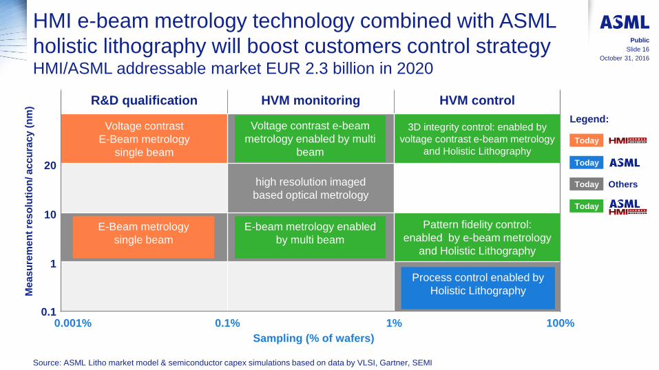
HMI e-beam metrology technology combined with ASML
holistic lithography will boost customers control strategy HMI/ASML addressable market EUR 2.3 billion in 2020
R&D qualification HVM monitoring HVM control
Voltage contrast
E-Beam metrology
single beam
3D integrity control: enabled by
voltage contrast e-beam metrology
and Holistic Lithography
high resolution imaged
based optical metrology
Pattern fidelity control:
enabled by e-beam metrology
and Holistic Lithography
Me
as
ure
me
nt
res
olu
tio
n/ a
cc
ura
cy (
nm
)
10
20
0.1
1
0.001% 0.1% 1%
Sampling (% of wafers)
Source: ASML Litho market model & semiconductor capex simulations based on data by VLSI, Gartner, SEMI
Today
Today
Today Others
Legend:
100%
Today
October 31, 2016
Public
Slide 16
E-Beam metrology
single beam
Process control enabled by
Holistic Lithography
Voltage contrast e-beam
metrology enabled by multi
beam
E-beam metrology enabled
by multi beam
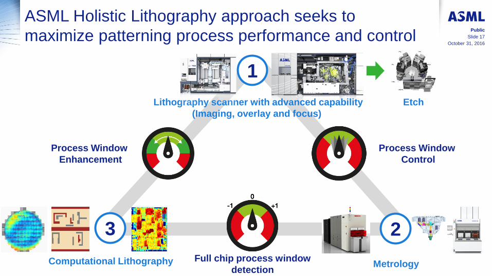
ASML Holistic Lithography approach seeks to
maximize patterning process performance and control
Full chip process window
detection
Process Window
Enhancement
Process Window
Control
Lithography scanner with advanced capability
(Imaging, overlay and focus)
Computational Lithography Metrology
1
3 2
Etch
October 31, 2016
Public
Slide 17
October 31, 2016
Slide 18
Public
Forward looking statements This document contains statements relating to certain projections and business trends that are forward-looking, including statements with respect to our outlook,
including expected customer demand in specified market segments (and underlying assumptions) including memory, logic and foundry, expected sales levels, trends,
including trends towards 2020 and beyond and expected industry growth, and outlook, systems backlog, expected or indicative market opportunity, financial results and
targets, including, for ASML and ASML and HMI combined, expected sales, other income, gross margin, R&D and SG&A expenses, capital expenditures, cash
conversion cycle, EPS and effective annualized tax rate, annual revenue opportunity and EPS potential by end of decade and growth opportunity beyond 2020 for
ASML and ASML and HMI combined, cost per function reduction and ASML system ASP, goals relating to gross cash balance and ASML’s capital structure, customer,
partner and industry roadmaps, productivity of our tools and systems performance, including EUV system performance (such as endurance tests), expected industry
trends and expected trends in the business environment, the addition of value through delivery of lithography products and the achievement of cost-effective shrink,
expected continued lithography demand and increasing lithography spend, the main drivers of lithography systems, lithography intensity for all market segments,
customer execution of shrink roadmaps, future memory application distribution, expected addressable markets, including the market for lithography systems and service
and options, expected manufacturing and process R&D, statements with respect to growing end markets that require fab capacity driving demand for ASML’s tools,
statements with respect to the acquisition of HMI by ASML, including market opportunity, the expected timing of completion of the HMI acquisition and delisting of HMI,
the expected benefits of the acquisition of HMI by ASML, including expected continuation of year on year growth, the provision of e-beam metrology capability and its
effect on holistic lithography solutions, including the introduction of a new class of pattern fidelity control and the improvement of customers’ control strategy, statements
with respect to EUV, including targets, such as availability, productivity, facilities and shipments, including the number of EUV systems expected to be shipped and
timing of shipments, and roadmaps, shrink being key driver to industry growth, expected industry adoption of EUV and statements with respect to plans of customers to
insert EUV into production and timing, the benefits of EUV, including expected cost reduction and cost-effective shrink, the expected continuation of Moore's law,
without slowing down, and that EUV will continue to enable Moore’s law and drive long term value, goals for holistic lithography, including pattern fidelity control,
expectations relating to double patterning, immersion and dry systems, intention to return excess cash to shareholders, statements about our proposed dividend,
dividend policy and intention to repurchase shares and statements with respect to the current share repurchase plan. You can generally identify these statements by the
use of words like "may", "will", "could", "should", "project", "believe", "anticipate", "expect", "plan", "estimate", "forecast", "potential", "intend", "continue" and variations of
these words or comparable words. These statements are not historical facts, but rather are based on current expectations, estimates, assumptions and projections
about the business and our future financial results and readers should not place undue reliance on them.
Forward-looking statements do not guarantee future performance and involve risks and uncertainties. These risks and uncertainties include, without limitation, economic
conditions, product demand and semiconductor equipment industry capacity, worldwide demand and manufacturing capacity utilization for semiconductors (the principal
product of our customer base), including the impact of general economic conditions on consumer confidence and demand for our customers' products, competitive
products and pricing, the impact of any manufacturing efficiencies and capacity constraints, performance of our systems, the continuing success of technology
advances and the related pace of new product development and customer acceptance of new products including EUV, the number and timing of EUV systems
expected to be shipped and recognized in revenue, delays in EUV systems production and development, our ability to enforce patents and protect intellectual property
rights, the risk of intellectual property litigation, availability of raw materials and critical manufacturing equipment, trade environment, changes in exchange rates,
changes in tax rates, available cash and liquidity, our ability to refinance our indebtedness, distributable reserves for dividend payments and share repurchases and
timing of resumption of the share repurchase plan, and other risks indicated in the risk factors included in ASML's Annual Report on Form 20-F and other filings with the
US Securities and Exchange Commission. These forward-looking statements are made only as of the date of this document. We do not undertake to update or revise
the forward-looking statements, whether as a result of new information, future events or otherwise.