Embed Size (px)
Citation preview

University of Central Florida University of Central Florida
STARS STARS
Electronic Theses and Dissertations
2019
Room Temperature VOx Air-Bridge Bolometer integrated with Room Temperature VOx Air-Bridge Bolometer integrated with
Metal-Insulator-Metal Resonant Absorbers Metal-Insulator-Metal Resonant Absorbers
Seth Calhoun University of Central Florida
Part of the Physics Commons
Find similar works at: https://stars.library.ucf.edu/etd
University of Central Florida Libraries http://library.ucf.edu
This Doctoral Dissertation (Open Access) is brought to you for free and open access by STARS. It has been accepted
for inclusion in Electronic Theses and Dissertations by an authorized administrator of STARS. For more information,
please contact [email protected].
STARS Citation STARS Citation Calhoun, Seth, "Room Temperature VOx Air-Bridge Bolometer integrated with Metal-Insulator-Metal Resonant Absorbers" (2019). Electronic Theses and Dissertations. 6833. https://stars.library.ucf.edu/etd/6833

ROOM TEMPERATURE VOX AIR-BRIDGE BOLOMETER INTEGRATED WITH
METAL-INSULATOR-METAL RESONANT ABSORBERS
by
SETH CALHOUN
B.S. University of Central Florida, 2015
A dissertation submitted in partial fulfillment of the requirements
for the degree of Doctor of Philosophy
in the Department of Physics
in the College of Sciences
at the University of Central Florida
Orlando, Florida
Summer Term
2019
Major Professor: Robert Peale

ii
© 2019 Seth Calhoun

iii
ABSTRACT
Spectrally-selective un-cooled micro-bolometers have many military and industrial
applications for infrared sensing and imaging, e.g. target acquisition and chemical
analysis. In this work, a micro-bolometer was fabricated with integrated wavelength-
selective absorber based on subwavelength metal-insulator-metal (MIM) resonators. The
fabricated air-bridge structure used a vanadium oxide thin film as the bolometric element.
A novel aqueous deposition method of depositing vanadium oxide was investigated and
compared to traditional sputtered vanadium oxide to determine achievable temperature
coefficient of resistance. The MIM absorber itself was investigated as a function of the
dielectric used, and the strong dependence of the resonance spectrum on dispersion was
revealed. Finally, the completed bolometers were characterized, and usual figures of
merit for thermal infrared detectors were determined. Unlike previous efforts this
research is aimed at putting the bolometer inside of the MIM absorber, thereby reducing
thermal mass and the thermal time constant compared to those bolometers where the
absorbers are just put on top.

iv
I dedicate this work to my parents, Janice and Richard, for sacrificing so much to give
myself, and my siblings, the opportunities we have had in life, and for being the best
parents in the universe. I also dedicate this to my sisters, Elyssa and Malorie and my
girlfriend, Lauren Persaud. Finally I dedicate this to my dogs, Bella and Angel

v
ACKNOWLEDGMENTS
First I would like to acknowledge my supervisor Dr. Robert Peale for mentoring and
advising me through not only my PhD but also my undergraduate work as well. I have
been given numerous amazing opportunities to advance my knowledge and skills due to
his tireless efforts. My funding can be directly attributed to his work and efforts. Dr.
Peale has created an open environment in his group and labs where I always felt like my
suggestions and questions were validated and encouraged. Without his advice and
encouragement I would not have the skills that allowed me the professional career
opportunities I now have.
I would like to acknowledge and thank my committee, Dr. Masahiro Ishigami, Dr.
Christopher Bennett and Dr. Sasan Fathpour for accepting and guiding me in my
dissertation.
I would like to thank the many lab and group mates who have helped me throughout my
PhD. Cameron Nickle, Dr. Pedro Figueriedo, Rachel Evans, Priyanka Vaidya, Dr.
Rebecca Cebulka, Dr. Tommy Boykin, and Brandon Blue, and so many more who I
know I am forgetting. I would like to thank each of these people, most of whom were not
in my group, for helping me with many different hurdles I encountered in my research.
A special thanks goes out to everyone who has helped me with learning and managing
the cleanroom facilities at UCF. In particular I would like to thank Guy Zummo for his
lessons and teachings. Without his acceptance of me as his apprentice I would be no
where near where I am today in terms of a professional career. A special thanks is also in

vi
order for Nathan Aultman, without his help in supporting the cleanroom I would have
never been able to complete my dissertation or my research on time. He has also taught
me invaluable lessons from his time working in industry facilities.
I would like to acknowledge, not just for this dissertation, but for helping me through my
whole life, my parents, Janice and Richard Calhoun, as well as my sisters Malorie
Calhoun-Daspit, and Elyssa Calhoun. You have all been my rock. You’re understanding
of the time and dedication I have put into this research has not been overlooked. The
understanding of all the holidays, family visits, and birthdays I have missed due to this
work has not gone unnoticed. I appreciate everything you have done for me in this time,
and the understanding you have all shown me, even if I don’t always show it well. You
all looked out for my well-being when I wasn’t and I hope one day I can repay you all in
turn.
My deepest and most heatfelt thank you goes to my girlfriend, Lauren Persaud. Lauren, I
met you 4 months before starting graduate school. You have been there though
everything. I could not have asked for a more understanding, loving, and caring person.
You reminded me of who I am when I was at my lowest. You stuck by me through the
worst, and best parts of grad school. It’s impossible for me to ever convey the gratitude I
have for you putting up with me these past four years. I can say, with utmost certainty, I
would not have gotten through graduate school if it had not been for your undying,
unwavering support and belief in me, and I will try the rest of my life to show you what
you mean to me. I love you.

vii
TABLE OF CONTENTS
LIST OF FIGURES ........................................................................................................... ix
LIST OF TABLES ............................................................................................................ xii
LIST OF ABBREVIATIONS .......................................................................................... xiii
CHAPTER ONE: INTRODUCTION ................................................................................. 1
CHAPTER TWO: THEORETICAL CONSIDERATIONS ............................................... 9
2.1 Material Considerations ............................................................................................ 9
2.1.1 Temperature Coefficient of Resistivity .............................................................. 9
2.1.2 Heat ................................................................................................................... 10
2.2 Bolometric FOM ..................................................................................................... 14
2.2.1 Responsivity ..................................................................................................... 14
2.2.2 NEP and D* ...................................................................................................... 16
2.2.3Noise Equivalent Temperature Dependence (NETD) ....................................... 17
2.3 MIM Absorbers ....................................................................................................... 17
2.3.1 MIM Overview ................................................................................................. 17
2.3.2 MIM standing-wave theory .............................................................................. 18
CHAPTER THREE: MIM ABSORBER DEVELOPMENT ........................................... 22
3.1 LWIR Dispersion .................................................................................................... 22
3.2 Simulation and Fabrication of MIM........................................................................ 26
3.2.1 Simulation ......................................................................................................... 26
3.2.2 Fabrication and characterization of MIMs ....................................................... 27
3.3 Results and Discussion ............................................................................................ 33
CHAPTER FOUR: SPRAY DEPOSITED AMORPHOUS VANADIUM OXIDE FOR
BOLOMETRIC APPLICATION ..................................................................................... 36
4.1 Streaming Process for Electrode-less Electrochemical Deposition ........................ 37

viii
4.2 Visual Characterization ........................................................................................... 38
4.3 SEM/AFM ............................................................................................................... 40
4.4 X-ray Diffraction ..................................................................................................... 42
4.5 TCR measurements ................................................................................................. 43
4.6 Summary ................................................................................................................. 45
CHAPTER FIVE: BOLOMETER FABRICATION AND INTEGRATION INTO MIM
........................................................................................................................................... 48
5.1 Index of Material of Thin Film Stack...................................................................... 48
5.2 Bolometer Fabrication Process and Consideration ................................................. 51
5.2.1 Bolometer Fabrication Techniques ................................................................... 52
5.3 MIMs-Bolometer-Integration process ..................................................................... 54
5.3.1 VOx Process Integration ................................................................................... 57
5.3.2 Top Metal Integration ....................................................................................... 59
5.3.3 Undercut with MIMs ........................................................................................ 60
CHAPTER SIX: BOLOMETER CHARACTERIZATION ............................................. 64
6.1 Experimental Methods ............................................................................................ 64
6.2 Measurements.......................................................................................................... 67
6.2.1 Noise Measurements......................................................................................... 67
6.2.2 Incident Power .................................................................................................. 69
6.2.3 Responsivity measurements ............................................................................. 71
6.3 FOM and Discussion ............................................................................................... 75
CHAPTER SEVEN: CONCLUSIONS ............................................................................ 76
7.1 Discussion ............................................................................................................... 76
7.2 Future Optimization and Experiments .................................................................... 77
APPENDIX: MY PUBLICATIONS ................................................................................ 79
LIST OF REFRENCES .................................................................................................... 82

ix
LIST OF FIGURES
Figure 1. Atmospheric transmission of infrared radiation .................................................. 2
Figure 2 Schematic of one MIM absorber cell ................................................................. 19
Figure 3 SiO2 index of refraction (blue) with graphical solutions to two different modes
of eq.32. in red and green.................................................................................................. 21
Figure 4 Optical Constants of silicon nitride, aluiminum nitride, silicon dioxide and
titanium dioxide. The MWIR and LWIR bandwidths have been highlighted. ................. 25
Figure 5. 2D LFDTD simulation results for AlN MIM devices with 50% duty cycle on
the top strips. Top left shows results for 100nm AlN, bottom left shows results for 150nm
AlN and the right shows results for a 200nm AlN layer................................................... 27
Figure 6 Optical microscope image of common artifacts that occurred while fabricating
the top metal structure of the MIMs. (left) rounding of the squares can be seen. (right)
shows the array connecting and becoming a continuous top layer. .................................. 29
Figure 7 Reflectivity rig inside of FTIR spectrometer used to measure absorption spectra
of the devices. ................................................................................................................... 30
Figure 8 SEM image of MIM devices with gold squares as the geometric array on top.. 31
Figure 9 Reflectance spectra of different MIM devices that utilize different dielectrics.
The green line represent AlN the black line represents TiO2 and the red line represents
SiO2. .................................................................................................................................. 33

x
Figure 10 Comparision of experimental, theoretical, and simulated values for resonances
for AlN (top left) and TiO2(bottom left) and SiO2 (right). ............................................... 35
Figure 11 SPEED deposited VOx samples done with different post deposition processing
........................................................................................................................................... 39
Figure 12 SEM image of SPEED deposited VOx sample 3 .............................................. 41
Figure 13 AFM image of SPEED deposited VOx sample 3 ............................................. 42
Figure 14 XRD data of SPEED deposited VOx films ...................................................... 43
Figure 15 Plot of the natural log of the sheet resistance vs temperature for different VOx
films .................................................................................................................................. 45
Figure 16 Refractive index and extinction coefficients obtained through ellipsometry for
SiO2/VOx/SiO2 thin film stacks. ........................................................................................ 50
Figure 17(left) complex and real values of the index of refraction of an AlN/VOx/AlN
thin-film stack, taken with IR ellipsometry. (right) complex and real values of the index
of refraction of AlN .......................................................................................................... 51
Figure 18 (left) Optical microscope image of AlN air bridge after etch back in KOH with
a positive photoresist mask.(right) Optical microscope image of etch backed AlN
protected by SU-8. ............................................................................................................ 56
Figure 19 Optical microscope image of AlN based bolometer after VOx has been
deposited and fabricated ................................................................................................... 58

xi
Figure 20 (top) AlN based bolometer with gold squares coating entire surface before au
etch back (bottom) same sample after gold etch back. ..................................................... 60
Figure 21 SEM image of a bolometer with the gold squares coated in protective
photoresist prior to being undercut ................................................................................... 62
Figure 22(left) SEM image at x800 of AlN MIM integrated bolometer array. (right) SEM
image at x3.5k of a single AlN MIM integrated bolometer showing full suspension from
the substrate ...................................................................................................................... 63
Figure 23 (left) Photograph of an AlN-MIMs integrated bolometer die mounted and wire
bonded to a ceramic chip carrier (right) photograph of an AlN-MIMs integrated
bolometer on a chip carrier mounted in a socket on a PCB .............................................. 65
Figure 24 Top-down photograph of experimental setup for bolometer characterization. 66
Figure 25 Noise of a 180MΩ bolometer biased at 2V. ..................................................... 69
Figure 26 Frequency Response of a 1.9MΩ bolometer .................................................... 72
Figure 27 Plot of blackbody temperature vs photo-response for a 1.9MΩ bolometer ..... 73
Figure 28 Photoresponse vs bias voltage. The effect shows a linear trend up to 3V. ....... 74

xii
LIST OF TABLES
Table 1 Characteristics of VOx Samples grown by SPEED ............................................. 47
Table 2 Table of MIMs integrated bolometers geometrical and electrical characterization
parameters and their FOM ................................................................................................ 75

xiii
LIST OF ABBREVIATIONS
Au Gold
CF4 Carbon Tetrafluoride
D* Normalized Detectivity
FTIR Fourier-Transform Infrared Spectroscopy
FPA Focal Plane Array
KOH Potassium Hydroxide
KRS-5 Thallium Bromo-Iodide
LWIR Long-Wave Infrared, 8-12µm
MIM Metal-Insulator-Metal Perfect Absorber
MWIR Mid-Wave Infrared, 3-5µm
NETD Noise-Equivalent Temperature Difference
NEP Noise-Equivalent Power

xiv
NiCr Nichrome (Nickel/Chrome 80/20)
O2 Oxygen
RIE Reactive Ion Ethcer
SEM Scanning Electron Microscope
SF6 Sulfur Hexafluoride
SNR
SPEED
Signal-to-Noise Ratio
Streaming Process for Electrodeless
Electrochemical Deposition
TCR Temperature Coefficient of Resistivity
TMAH Tetramethyl Ammonium Hydroxisw
VOx Amorphous Vanadium Oxide

1
CHAPTER ONE: INTRODUCTION
Infrared radiation has been known about since 1800 when, through measuring temperature,
William Herschel noticed an increase in power radiated past the visible spectrum into what we
now know as the infrared spectrum. Since then research into infrared radiation have resulted in
some of the fundamental physics we learn today.
The atmosphere on earth limits the transmission wavelengths of infrared radiation, due to certain
molecules in our atmosphere absorbing part of the radiation before it reaches us. There are three
main bands of infrared radiation that our atmosphere transmits. The short-wave IR (SWIR)
consists of 0.75-2.5µm, mid-wave IR (MWIR) consisting of 3-5 µm and the long-wave IR which
includes 8-14 µm wavelengths. Figure 1 presents a graphical representation of these transmission
windows.

2
Figure 1. Atmospheric transmission of infrared radiation
Since its discovery the detection of infrared radiation has been a heavily researched fields with
advancements happening rather quickly. In general two types of infrared detectors exist,
thermistor detectors and photon detectors. While both detect incident radiation they go about it in
very different physical manners. Photon detectors work off of bound electrons being excited by
incident radiation these electrons will create an increased conductivity along the detector which
can be measured by either measuring voltage with a constant current or by measuring current
with a constant voltage supply. Thermal detectors, also known as thermistors work on the
principle of converting incident radiation to thermal energy. This thermal energy can change the
electrical properties of such devices, these changes can be measured and through this information
about the incident radiation can be obtained.
The most common type of thermistor infrared detector is a microbolometer. A microbolometer is
a device where incident radiation is converted into heat, this heat changes the resistance of the
bolometric element (The material in the device that is actually changing due to radiation) which

3
can be measured by simply measuring voltage while applying a constant current. Due to
microbolometers principle detection mechanic relying on small changes in heat, thermal isolation
of the detectors is usually necessary to increase sensitivity [1]. The need for this thermal isolation
has resulted in many different geometries, materials, and structures to be used in the fabrication
of these devices [2]–[4]One of the most common, which is employed in this research is forming
a self-supporting air-bridge[5]–[9]. An air bridge is formed by having a device that is free
standing (nothing touching underneath or above it) and is connected to the bulk of the device
through only thin arms for electrical connections to the device. This means the only way for the
heat to dissipate through the device (assuming the device is under vacuum) is through the thin
arms. It is worth noting that if this were an uncooled microbolometer this problem could be
solved by cooling the microbolometer array to get rid of any unwanted background noise, the
large disadvantage to this is the cost of having a cryogenically cooled device as well as the
inability to put a cryogenic cooling system into a compact, field-ready device. This makes
uncooled thermal detectors a more cost efficient, and better option for military and active field-
related situations.
Microbolometers are made using silicon processing and manufacturing techniques. As
mentioned earlier bolometers thermal mass needs to be minimized. Commercial
microbolometers will have a dielectric membrane on-top of which the active bolometric element
will sit. Another very thin layer of dielectric is usually put on top of the devices to ensure that no
damage, or oxidation, will happen to the bolometric element. This device is then made to be
suspended from the substrate, or lifted off of the substrate in a cantilever fashion attached to the

4
substrate through a set of thin arms that are used to measure the output signal from the bolometer
as well as provide a path of thermal conductance [1].
The active bolometric element is the most essential, and most studied aspect of the
microbolometer. The bolometric element is the material within the device whose resistance
changes with the absorption of incident radiation, it normally a dielectric, or sometimes a pure
metal. It is the part of the device that is actually producing the output voltage. The most common
figure of merit (FOM) of the bolometric element is it’s TCR (temperature coefficient of
resistance). TCR is a measure of the amount the resistance of a material changes due to heat.
Every materials resistance changes due to heat, in pure metals the resistance will increase as
temperature increases, in a semiconductor the resistance will decrease with temperature rise [10].
In a microbolometer an active element with a high TCR, meaning that the temperature changes
greatly with little heat change, is desired, while also maintaining a low resistance as higher
resistances can lead to larger noise. In semiconductors the TCR is negative, while in metals it is
positive. The higher the TCR of the active film the higher the sensitivity of the microbolometer
that could be made. Numerous amounts of different materials, metals and semiconductors alike
have been studied for use in micro-bolometers; perovskites [11], carbon nanotubes [12],
platinum [13], germanium [14], tellurium oxide [15] and others.
For a long time the most prevalent and studied material to be used in microbolometers was
vanadium oxide [1], [16]–[21]. VOx exhibits a high TCR, and has a fairly low resistivity, which
is needed to reduce electrical noise in the device. These qualities made it an easy choice for
Honeywell when they started to make the first commercially available microbolometers.

5
Amorphous VOx is used as compared to its crystalline counterpart because the single crystal
vanadium oxide films usually exhibit a sharp insulator to metal transition which results in a non-
linear hysteresis effect which is not desirable for microbolometers as this will result in data that
can be hard to interpret [22]. Alternatively amorphous VOx shows a much more linear TCR with
no sharp metal-to-insulator transition noted. Within the last decade amorphous Si has quickly
become comparable to VOx in use within microbolometers. Hydrogenated amorphous silicon
offers high TCR, a high absorption in the infrared and is compatible with silicon fabrication
processes. The hydrogenation is needed to passivate the silicon and make sure the resistance is in
a reasonable range for a microbolometer [1], [23], [24]. Amorphous silicon’s TCR is also heavily
effected by doping concentration and other properties [25]. Unlike VOx processing which would
only require conventional DC or RF sputtering though, amorphous Si requires PECVD
deposition on the wafer.
Microbolometers have been extensively researched in the last 40 years, theoretical limits on
figures of merits have started to be reached for uncooled-microbolometers. While research has
been extensive there is a growing need for narrow-band wavelength selective microbolometers
[26]. With a narrow-band detector, detailed information can be obtained from infrared source.
Radiative signatures of different chemical compositions can be detected which is extremely
useful in target acquisition for military applications.
Normally, in a broadband microbolometer the material surrounding the bolometric element
(conventionally a thin dielectric), as well as the bolometric element will all absorb infrared
radiation, when absorbed the radiant energy heats the device in turn will creating a change in the

6
materials’ resistance. In order for a narrow-band microbolometer to be achieved, the device must
have a significantly different output when a certain wavelength is absorbed, i.e. the resistance
has to change more significantly at this wavelength band than other wavelengths. Meaning more
of the energy needs to be absorbed and converted to heat at specific wavelengths in order for the
bolometric elements temperature change to be larger at this wavelength than others. One method
to a accomplish this is integrating a bolometer into an infrared absorbing structure.
Different types of electromagnetic absorbers exist for use as an absorbing structure, these include
Fabry-Perot type resonators like a Salisbury screen, and surface plasmon-polariton
resonators[27]–[30]. Metal-insulator-metal (MIM) absorbers are a quickly growing field [31].
These structures consist of thin film stacks, the whole stack can be treated as its’ own material
with an effective permittivity and effective permeability [32]. These effective properties stem
from the constituent units of the stack, their geometry, size and periodicity will all effect the
electro-optical properties of the material. MIM devices have gained extreme interest in many
different areas including antennas, absorbers and superlenses (lens’ that go past the diffraction
limit) [33]–[35]. In recent years MIM absorbers have been shown to be able to achieve near
100% absorption in multiple bandwidths including the near, mid, and far wave infrared, this
makes meta-material absorbers a much more interesting option for opto-electronic devices.
MIMs (metal-insulator-metal) are made by creating a conducting, optical thick ground-plane this
material needs near 100% reflection in the wavelength range being targeted, a dielectric layer,
and a layer of metal periodic structures[31], [32], [36], [37]. Usually a periodic array of
geometric structures is patterned as the top metal layer. Many different geometries have been

7
used for the top periodic structure, including squares, circles, and complex nano-antennas [31],
[38], [39].Commonly split-ring resonators (SRR) are used as well, though these are mainly used
for the terahertz to giga-terahertz range [31], [40]. In this research square gold arrays were made
as the top periodic structure.
Although absorption is known to occur in these structures, and it has been shown that the
geometry of the top periodic structure as well as the materials chosen have an effect on where
this resonant absorption occurs, very few analytical theories been formed to explain this
phenomenon in the IR range. Most theories are solved numerical and simulation approaches[41],
[42]. In this work we discuss an analytical standing wave theory to explain the resonances and
study its validity in the mid and long-wave infrared ranges [43].
The aim of this research is to improve and reduce an already patented design for a wavelength
selective thermal detector by integration of a VOx air-bridge bolometers and MIM absorbers to
realize a spectrally selective microbolometer within the LW and MWIR regimes[44]. Unlike
previous efforts done to realize these devices this research will put the bolometer inside of the
MIM absorber rather than putting the absorber on-top of the bolometer [45]. This is to reduce
thermal mass and have a more sensitive bolometer. Chapter 2 will provide theoretical
background on the operation, responsivity and FOM of microbolometers as well as the
theoretical concepts involved in the MIM absorbers. Chapter 3 discusses the fabrication of the
MIMs and the study of the choice of dielectrics dependence on resonance spectrum. In this
chapter MIMs are developed and characterized for their resonance spectra. These resonance
spectra are compared with simulations and theory. Chapter 4 presents a novel deposition method

8
for depositing vanadium oxide, SPEED. Amorphous vanadium oxide films are deposited by
SPEED, these films are characterized for bolometric FOM and compared to those of
conventionally sputtered VOx. Chapter 5 introduces the process by which the integrated
bolometer is fabricated as well as the studies and challenges with the integration process.
Chapter 6 discusses the characterization of the integrated bolometers, including the experimental
methods that were used to characterize them and the FOM that were found. Chapter 7 concludes
this paper by giving a summary of the research and the methods used as well as providing
possibilities for future research that could be done to optimize these devices further.

9
CHAPTER TWO: THEORETICAL CONSIDERATIONS
2.1 Material Considerations
2.1.1 Temperature Coefficient of Resistivity
A materials resistances can be viewed as a function of temperature defined by [46],
𝑅(𝑇) = 𝑅0(1+∝ ∆𝑇) (1)
In this equation ΔT = T – T0, R0 is the materials resistance at temperature T0, and α is the TCR of
the material. TCR can be represented as
𝛼 =1
𝑅
𝑑𝑅
𝑑𝑇 (2)
Most conventional micro-bolometers utilize semiconductors as their bolometric element due to
the higher magnitude TCR that can be achieved in semiconductors than metals. Materials with
large magnitude TCRs are desirable for bolometers. Larger TCR material will lead to a
bolometers resistance changing greatly with comparatively small temperature changes, i.e a more
sensitive bolometer. Amorphous Vanadium oxide is a common material used in the
manufacturing of microbolometers due to its high TCR. VOx can have a TCR ranging from 2%-
4% depending on the structure of the material [1].Its’ TCR is extremely dependent upon its’
structure. The deposition technique used to deposit the vanadium oxide has a large impact on its
structure and electrical properties .. While sputtering is a very common method many different
types of deposition methods for vanadium oxide exist. These include spray pyrolosis [47], pulsed
laser deposition[17] and sol-gel deposition [48]. Each of these deposition methods would need to

10
be tested for material properties and TCR before considering use in a microbolometer.
Amorphous. It is of note that for TCR to be useful in a bolometer, the TCR over the target
temperature range needs to be as linear as possible. VO2 is not used for this reason as it has a
sharp metal-to-insulator transition at approximately 68o C, this effect is a non-linear hysteresis
effect [22].
2.1.2 Heat
A bolometers ability to sense IR stems from incident radiant power creating a temperature
change in the device, thus changing a thin film’s (contained inside the device) resistance. To
determine how much the temperature of the device will change with incident radiation we must
look at the system as a thermodynamic system. By convention E will represent the internal
energy of a body, W represents the work done on the system and Q represents the heat
transferred either in or out of the system through contact with other bodies. The energy change
per unit time of this system is then calculated through [49]
𝑑𝐸
𝑑𝑡=
𝑑𝑊
𝑑𝑡+
𝑑𝑄
𝑑𝑡 (5)
Assuming that there is no work done on the system from surrounding sources then dW/dt=0 this
leads equation 5 to read

11
𝑑𝐸
𝑑𝑡=
𝑑𝑄
𝑑𝑡 (6)
This equation will be negative if heat was flowing out of the body and positive if heat was
flowing into the body.
. Heat capacity, represented as C, is the amount of thermal energy required to raise the
temperature of a system by one unit and can be written as
𝐶𝑑∆𝑇
𝑑𝑡=
𝑑𝑄
𝑑𝑡 (7)
The change in heat per unit time, i.e. the right side of the Eq 7, of this system can be written as
𝑑𝑄
𝑑𝑡= −𝐺∆𝑇 + 𝜂𝑃𝑖 (8)
Here G is the thermal conductance of a material; a material property and will depend on the
geometry and material of the device. ΔT is the temperature difference between the detector and
the bulk heat sync. Pi represents the incident power on the detector which is the source of the
heat, this term will be derived later in section 5.1.2. The last variable, η represents the
absorbtance, which has a value between 0 and 1.
Replacing the left side of equation 8 with equation 7 we generate the equation
𝐶𝑑∆𝑇
𝑑𝑡= −𝐺∆𝑇 + 𝜂𝑃𝑖 (9)
This equation will be used to calculate the thermal characteristics of the device, it stems from the
conservation of energy and is called the heat balance equation.

12
The incident power in equation 9 is assumed to be wave-like in modulation. This is achieved
physically through use of an optical chopper. Thus Pi can be written as Pi=Pieiωt where the
modulation frequency is ω=2πf.
Equation 9 is not complete when a bias is run through a device, the natural resistance of the
materials will cause the temperature of the device to rise. This thermal noise is known as joule
heating, and is calculated as i2R. In the case of the load resistor circuit used for testing the
bolometers the joule heating term, is
𝑖2𝑅 =𝑉𝑏
2𝑅
(𝑅𝑙+𝑅)2 (10)
Where Rl is the resistance of the load resistor, R is the bolometers resistance and Vb is the
voltage bias applied. Accounting for the joule heating term equation 9 becomes
𝐶𝑑∆𝑇
𝑑𝑡= −𝐺∆𝑇 + 𝜂𝑃𝑖 +
𝑑(𝑖2𝑅)
𝑑𝑡= −𝐺∆𝑇 + 𝑃𝑖𝑒𝑖𝜔𝑡 +
𝑉𝑏2𝑅
(𝑅𝑙+𝑅)2 (11)
If we assume that the system is isolated and there is no external power being supplied to the
detector, i.e. Pi=0 and therefore there is no change in temperature, then equation 11 reads
𝐺0∆𝑇 = 𝑖2𝑅 =𝑉𝑏
2𝑅
(𝑅𝑙+𝑅)3 (12)
Where G0 is the average thermal conductance at temperature T0.
When we account for the incident power from an external source equation 12 becomes more
complicated as the joule heating term is resistant dependent. Resistance as has been stated is a
function of temperature. Taking the derivative of the joule heating with respect to temperature
equation 10 becomes

13
𝑑
𝑑𝑅(𝑖2𝑅)
𝑑𝑅
𝑑𝑇= 𝛼𝑅
𝑑
𝑑𝑅(
𝑉𝑏2𝑅
(𝑅𝑙+𝑅)2) =𝑉𝑏
2𝑅∝(𝑅𝑙−𝑅)
(𝑅𝑙+𝑅)2 (13)
This makes the full heat balance equation
𝐶𝑑∆𝑇
𝑑𝑡+ [𝐺 −
𝑉𝑏2𝑅𝛼(𝑅𝑙−𝑅)
(𝑅𝑙+𝑅)3 ] ∆𝑇 = 𝜂𝑃𝑖 (14)
This can be rewritten as
𝐶𝑑∆𝑇
𝑑𝑡+ 𝐺𝑒𝑓𝑓∆𝑇 = 𝜂𝑃𝑖 (15)
Equation 15 is a first-order inhomogeneous differential equation whose solution is of the form
Aeiωt. The solution in this form of equation 15 is
𝑇𝑒−𝐺𝑒𝑓𝑓
𝐶𝑡 +
𝑃𝑖𝜂
𝐺+𝑖𝜔𝐶= ∆𝑇 (16)
Taking the real part of equation 16 results in
|∆𝑇| =𝑃𝑖𝜂
𝐺√1+𝜔2(𝐶
𝐺𝑒𝑓𝑓)2
(17)
In equation 17, the term under the square root in the parentheses is known as the thermal time
constant
𝜏𝑡ℎ =𝐶
𝐺𝑒𝑓𝑓 (18)
This thermal time constant is a measurement of how quickly the device will take to respond to a
change in its temperature, i.e. the relaxation time. This will be an important measurement that
effects the response time of the bolometers.

14
2.2 Bolometric FOM
2.2.1 Responsivity
Responsivity, Rv,which is a measurement of the voltage response in terms of incident power on
the detector. While it is not a standardized FOM it is a device characteristic that will directly
affect the FOMs of the bolometer. Mathematically it is written as
𝑅𝑣 =𝑑𝑉𝑜𝑢𝑡
𝑃𝑖 (19)
To calculate the output voltage of the device the circuit the bolometer is part of and where the
measurement of the bolometer is taken from need to be discussed. The bolometer is in a voltage
divider circuit. A DC bias source is used to bias the circuit and the bolometer and a load resistor
are in series with each other as seen in figure 1. In such a circuit the voltage across the resistor is
given by
𝑉𝑂𝑢𝑡 =𝑉𝑏𝑅
𝑅𝑙+𝑅 (20)
This leads to
𝑑𝑉𝑜𝑢𝑡 =𝑉𝑏𝑅𝑙
(𝑅𝑙+𝑅)2 𝑑𝑅 (21)
In the case of the experimental setup used the load resistor was impedance matched to the
bolometer being used so that Rl≈R. Using this it can be approximated
𝑅𝑙
(𝑅𝑙+𝑅)2 ≈1
4𝑅 (22)
Inserting equation 22 into equation 21 yields
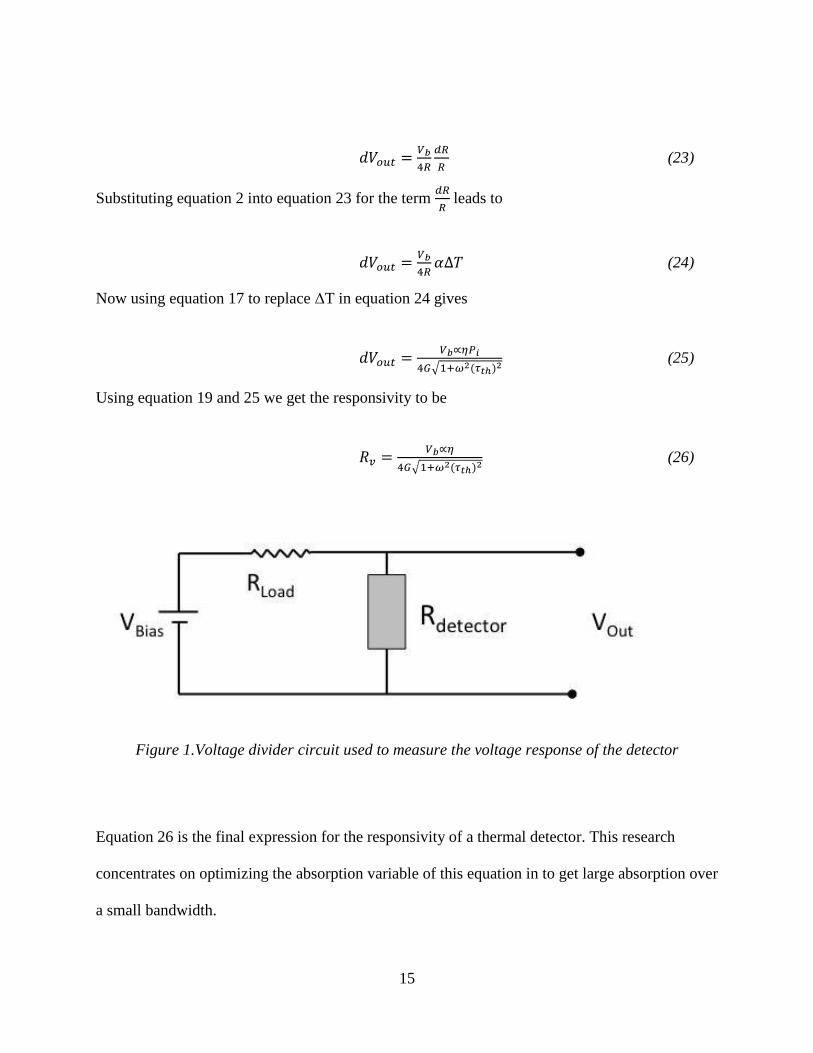
15
𝑑𝑉𝑜𝑢𝑡 =𝑉𝑏
4𝑅
𝑑𝑅
𝑅 (23)
Substituting equation 2 into equation 23 for the term 𝑑𝑅
𝑅 leads to
𝑑𝑉𝑜𝑢𝑡 =𝑉𝑏
4𝑅𝛼∆𝑇 (24)
Now using equation 17 to replace ΔT in equation 24 gives
𝑑𝑉𝑜𝑢𝑡 =𝑉𝑏∝𝜂𝑃𝑖
4𝐺√1+𝜔2(𝜏𝑡ℎ)2 (25)
Using equation 19 and 25 we get the responsivity to be
𝑅𝑣 =𝑉𝑏∝𝜂
4𝐺√1+𝜔2(𝜏𝑡ℎ)2 (26)
Figure 1.Voltage divider circuit used to measure the voltage response of the detector
Equation 26 is the final expression for the responsivity of a thermal detector. This research
concentrates on optimizing the absorption variable of this equation in to get large absorption over
a small bandwidth.

16
2.2.2 NEP and D*
One of the most important FOM of a bolometer is the Noise Equivalent Power (NEP). NEP is the
minimum amount of radiation needed for the device to detect the radiation above the background
noise. NEP is defined as [46]
𝑁𝐸𝑃 =𝑉𝑁𝑜𝑖𝑠𝑒
𝑅𝑉 (27)
A more technical definition of NEP is the signal to noise ratio (SNR) of 1 in a 1Hz output
bandwidth, i.e. the amount of incident radiation needed for an SNR of 1. The NEP of a detector
is dependent upon many parameters, including the detector area, and the noise equivalent
bandwidth, ∆𝑓. The noise equivalent bandwidth is a factor that depends upon the measurement
technique used. In the case of the lock in amplifier, the frequency bandwidth corresponds to the
integration time used
As NEP is dependent upon the size of the bolometer and the measurement technique used it is
not a standardized measurement and therefore makes it useless in comparing two bolometers. To
remedy this situation a FOM was made to normalize NEP for detector area and the noise
equivalent bandwidth. The normalized detectivity, often referred to as just detectivity is defined
as [46]
𝐷∗ =√∆𝑓√𝐴𝑑
𝑁𝐸𝑃 (28)
Another reason to make a normalized FOM is that it is always desirable to have a FOM where
larger numbers corresponds to a better value, while NEP is not like this D* is, where a higher D*
is more desirable.

17
2.2.3Noise Equivalent Temperature Dependence (NETD)
Noise Equivalent Temperature Dependence (NETD), is a measurement of the smallest
temperature difference that can be detected by the detector. Similar to the NEP but instead of
seeing what incident power creates a SNR of 1 the NETD looks at what temperature difference
results in a SNR of 1. NETD for an imaging system is defined by
𝑁𝐸𝑇𝐷 =∆𝑇
𝑆𝑁𝑅 (29)
NETD is an important FOM when looking at an imaging system due to its inherent limiting of
resolution. The lower the NETD value of the imaging array the higher the higher the possible
resolution of the image. NETD for a single pixel element can be calculated using a simple optical
setup example. In the end the NETD can be calculated by determining the D* of the devices.
Improving D* will by proxy improve the NETD and therefore optimization of a micro-bolometer
should begin with optimizing the D* of the device.
2.3 MIM Absorbers
2.3.1 MIM Overview
Absorption is a key characteristic of any micro bolometer and is extremely important in
wavelength selective bolometer. Many different types of absorbers exist with different
absorbance bands. In the case of this research LWIR and MWIR regime were targeted. Metal-
insulator-metal (MIM) perfect absorbers show absorbance within both of these ranges. MIMs fall
under a classification of absorbers known as metamaterial perfect absorber (MPA). MPA are
called perfect absorbers as they have been shown to have up to 99% absorption in many different
18
wavelength ranges[50]–[53]. MIMs from the bottom up consist of three layers; an optically
thick, conducting ground plane, a dielectric layer and a top surface array of conducting
structures. Absorbed wavelengths have significant dependence on the dimensions of this top
structure[53], [54]. Larger wavelengths (GHz, THz) allow for larger structures and therefore
complex structures can be placed using simple lithography[55]. For smaller wavelengths smaller
feature sizes are necessary making photolithography of complex structures more difficult. Due to
this most IR MIM absorbers utilize a periodic array of fundamental geometric shapes[31]. In the
MIMs in this research an array of gold squares was utilized.
The physical explanation of the absorption mechanism of these structures vary from source to
source. Some of the most common theories are LC-circuit theory[56] and planar wave guide
theory[41]. These theories display numerical simulations without presenting an analytical way to
solve the characteristic resonances or other features of the absorber. In this research an analytical
standing wave theory was utilized and tested for validity in this wavelength regime.
2.3.2 MIM standing-wave theory
The standing wave model used here has two conditions; That each until cell of the top surface
array is an independent, non-interacting absorber and two, that each unit cell is a MIM cavity
where standing wave resonances are trapped[43], [51]. The theory itself stems from a planar
wave-guide model introduced by Peng, et all. The standing wave model however presents a
derived analytical model to calculate resonances unlike other theories that utilize numerical
simulation.

19
In this theory incident TM radiation on the top metal structures creates a standing wave
underneath the top metal structure. Figure 2 presents a cross sectional view of one absorber, or
unit cell. The white and black lines represent two different harmonics of standing waves, the
white has three bounces while the black has one.
Figure 2 Schematic of one MIM absorber cell
The equation representing the resonances of these devices reads
𝜆(𝑏, 𝑚) =2(𝑏+1)𝑛(𝜆)
𝑏+2𝑚√𝑡2 +
𝑙2
(𝑏+1)2 (30)
Where m represents the order of the resonance being found and is a positive integer. “b” is a
representation of the number of “bounces” or reflections occur within the MIM structure. n
represents the dielectrics index of refraction, l is the lateral dimension of the top structure and t is
the thickness of the dielectric. This equation is derived simply through optical path length and
ray optics.
The strongest mode of these resonances is the fundamental resonance where m=0 and b=1,
visually it is represented as the black ray trace in figure 2. Mathematically equation 30 becomes

20
𝜆(1,0) = 4𝑛(𝜆)√𝑡2 +𝑙2
4 (31)
This is the main resonance mode that will be observed in research for this paper.
To solve this equation there are two methods, one uses numerical simulations, the other utilizes
graphical solutions. For the graphical solution equation 31 can be solved for the index of
refraction. Through experimental characterization (ellipsometry) or literature values the index of
refraction of the material can be plotted. If a graph of the index of refraction is obtained, then
solving equation 31 for n(λ) gives
𝑛(𝜆) =𝜆(𝑏+2𝑚)
2(𝑏+1)√𝑡2+𝑙2
(𝑏+1)2
(32)
By putting different b and m values, like 1 and 0 a linear equation can be formed between index
of refraction and wavelength. By putting this equation overlaid on the index of refraction graph
the resonant wavelengths can be to be at the intersection of these lines. Figure 3 displays an
example of how eq. 32 is solved graphically. The blue trace represents the index of refraction of
SiO2 while the green and red lines are linear equations stemming from eq 32. The intersection
points of these traces show the resonance wavelength values according to the standing wave
model.

21
Figure 3 SiO2 index of refraction (blue) with graphical solutions to two different modes of eq.32.
in red and green
22
CHAPTER THREE: MIM ABSORBER DEVELOPMENT
Optimization of the dielectric material was needed in order to ensure single resonance within the
LWIR was possible. Multiple resonances within this range are unwanted as they can lead to
broadening of the absorbance peak.
3.1 LWIR Dispersion
When considering what material to use for the dielectric layer many were considered. The
dielectric chosen had to be able to work in both the micro-bolometer and it’s fabrication as well
as being a good fit for the MIM structure. The initial consideration was using silicon dioxide due
to its’ ease of deposition, common use in CMOS and semi-conductor manufacturing, and
bolometers of these design had been fabricated before utilizing SiO2 [57].
MIM devices were fabricated using SiO2 as the dielectric and their resonances where
characterized. In Figure 7 the red data trace shows the resonance spectrum of a SiO2 MIM. This
absorbance spectra is extremely complicated within the regions needed. The reason for this
complex spectrum is a dispersion feature in SiO2 that occurs right in the LWIR regime[58].
Figure 4 shows optical constants for different dielectrics studied. The red plot represents SiO2’s
optical constants, within the 8-12µm range the dispersion feature can be seen. This non-
monotonic feature gives up to 3 resonances within the LWIR, making SiO2 MIMs ideal for
increasing absorbance across the whole LWIR but unwanted in a selective bolometer.

23
Other dielectrics were investigate for application in the device. Dielectrics were looked at for
their ease of integration into fabrication process and their index of refraction was studied for any
dispersion that could lead to parasitic resonances.
Using these criteria we compared three different dielectrics as well as silicon dioxide. Silicon
Nitride, silicon dioxide, titanium dioxide and aluminum nitride. These materials are suitable
within the semi-conductor fabrication techniques used to develop these devices. The constants
other than silicon nitride, were measured using an IR ellipsometer to find the complex constants
within the 2-15µm range. Woolam WVASE32 software was used to model the permittivity to
match the ellipsometry data. Peaks in the extinction coefficient correspond to a derivative
dispersion feature in the index of refraction at the same wavelength. It is apparent that silicon
dioxide has a very sharp extinction peak and therefore a derivative feature centered in the LWIR
regime. Silicon nitride, while not as large of a feature does have a small dispersion feature within
the LWIR s, if one can imagine drawing straight linear lines starting at the origin (like how the
graphical solutions are found), then it is easy to see that while mostly the graphs will only
intersect once in the LWIR, there are places where up to two intersections can occur if the slope
was steep enough. TiO2 has absolutely no dispersive like features within the desired range
making it a good fit for the devices. AlN shows a sharp extinction peak and corresponding
dispersion feature, but they are just past the LWIR range. Within the LWIR AlN shows a very
simple trace making it suitable for the wavelength-selective devices just like TiO2.
Looking at the MWIR regime of TiO2 and AlN, both monotonically change and have very
similar features, just offset. Equation 30 shows that at smaller wavelengths the lateral size of the
24
top feature must be sub-micron which makes contact photolithography; the method used for
fabrication of these devices; more difficult. To alleviate this problem the dielectric with the
lowest index of refraction within the MWIR should be chosen, as the lowest index material will
exhibit smallest resonance wavelength if the array dimensions are kept constant. SiO2 shows the
lowest index of refraction, but as stated before SiO2 is not suitable for wavelength selective
devices within the LWIR. The next lowest would be AlN and following that would be TiO2
.After these results simulations and experiments were done utilizing AlN and TiO2 to compare
theory simulation experiment and determine which dielectric suite this device.

25
Figure 4 Optical Constants of silicon nitride, aluiminum nitride, silicon dioxide and titanium
dioxide. The MWIR and LWIR bandwidths have been highlighted.
26
3.2 Simulation and Fabrication of MIM
3.2.1 Simulation
Simulations of the MIM devices were done for both TiO2 and AlN based absorbers. The
simulation was done utilizing LFDTD (Lumerical Finite-Difference Time-Domain) software.
Simulations modeled the top structures as infinitely long periodic strips as opposed to squares
which are actually on the device due to computing power and time restrictions, as 3 dimensional
simulations are extremely taxing on resources 3D simulations were done for one set of squares to
compare the results to that of the corresponding simulation with the stripes. The results of the 3D
simulation showed the resonant absorbance’s to be nearly the same and therefore 2D simulations
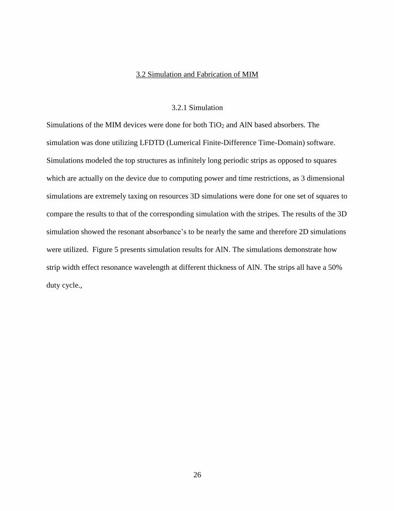
were utilized. Figure 5 presents simulation results for AlN. The simulations demonstrate how
strip width effect resonance wavelength at different thickness of AlN. The strips all have a 50%
duty cycle.,

27
Figure 5. 2D LFDTD simulation results for AlN MIM devices with 50% duty cycle on the top
strips. Top left shows results for 100nm AlN, bottom left shows results for 150nm AlN and the
right shows results for a 200nm AlN layer.
3.2.2 Fabrication and characterization of MIMs
MIMS were fabricated using standard semiconductor fabrication techniques. The initial ground
plane of Ti or Al was electron beam (e-beam) evaporated onto a silicon wafer. The deposition
28
technique used for the dielectric layer differed from dielectric to dielectric. Titanium dioxide was
e-beam evaporated onto the silicon wafer, while AlN was reactively sputtered using DC
sputtering of an aluminum target in an Ar/N2 mixture. The top metal array of squares was
patterned using contact photo-lithography. Gold was used as the top metal and was deposited
with e-beam evaporation.
Fabrication of the top metal squares was especially difficult. The nominal size and period of the
array needed make contact photolithography very sensitive to any type of anomaly or change in
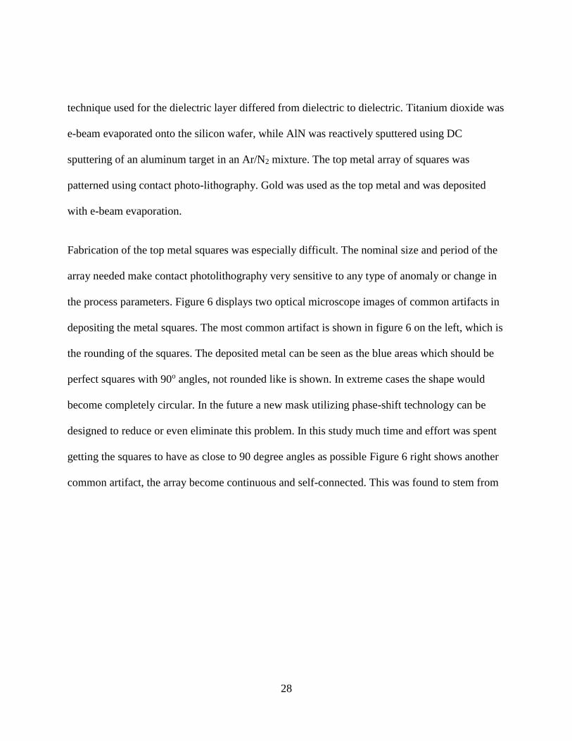
the process parameters. Figure 6 displays two optical microscope images of common artifacts in
depositing the metal squares. The most common artifact is shown in figure 6 on the left, which is
the rounding of the squares. The deposited metal can be seen as the blue areas which should be
perfect squares with 90o angles, not rounded like is shown. In extreme cases the shape would
become completely circular. In the future a new mask utilizing phase-shift technology can be
designed to reduce or even eliminate this problem. In this study much time and effort was spent
getting the squares to have as close to 90 degree angles as possible Figure 6 right shows another
common artifact, the array become continuous and self-connected. This was found to stem from
29
small variations in exposure dose as well as development time.
Figure 6 Optical microscope image of common artifacts that occurred while fabricating the top
metal structure of the MIMs. (left) rounding of the squares can be seen. (right) shows the array
connecting and becoming a continuous top layer.
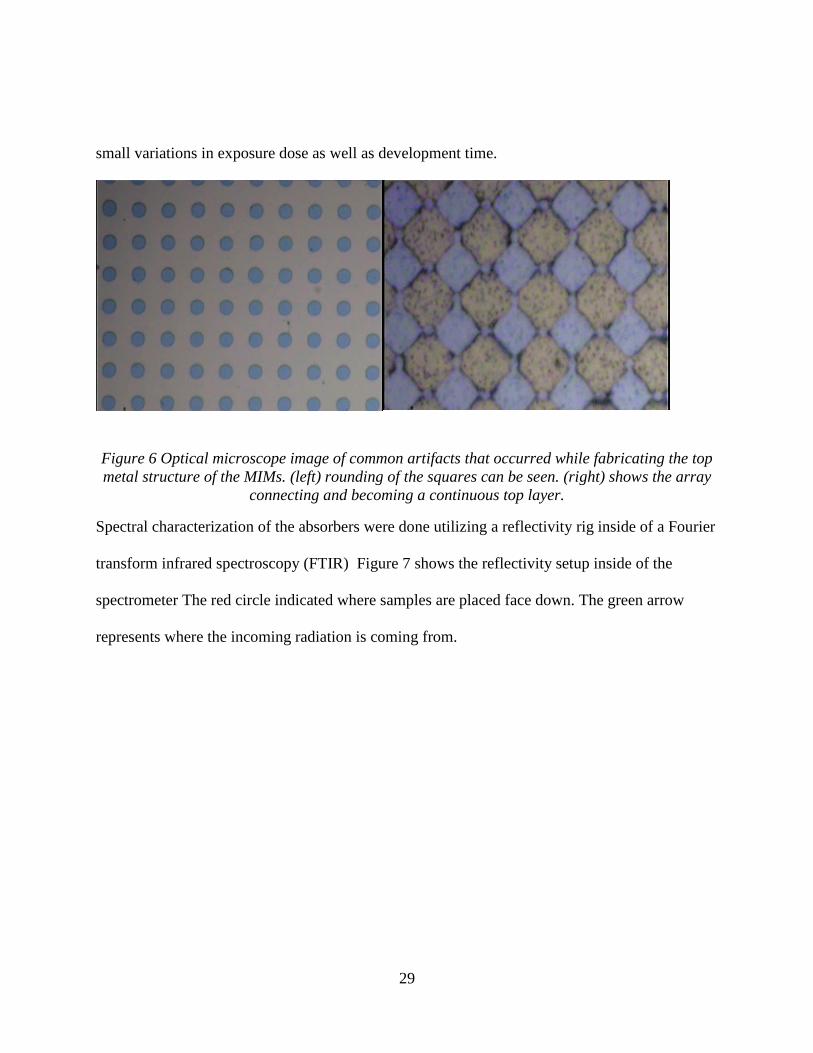
Spectral characterization of the absorbers were done utilizing a reflectivity rig inside of a Fourier
transform infrared spectroscopy (FTIR) Figure 7 shows the reflectivity setup inside of the
spectrometer The red circle indicated where samples are placed face down. The green arrow
represents where the incoming radiation is coming from.

30
Figure 7 Reflectivity rig inside of FTIR spectrometer used to measure absorption spectra of the
devices.
Metrology characterization was done through scanning electron microscopy (SEM). SEM
characterized the dimension of the deposited squares as well as checked the squares for
uniformity and squareness. Figure 8 shows an SEM image of one set of MIM absorbers. The

31
rounded corners were apparent in all arrays to some degree and come from an artifact of doing
sharp angle photolithography at such a small scale. The sample in figure 8 displays a sample
with good corners compared to others. In the case of these absorbers the nominal size of the top
structure measured to be approximately 2.5µm
Figure 8 SEM image of MIM devices with gold squares as the geometric array on top
Wavelength resonances and spectral absorbance of the device were characterized using FTIR
spectroscopy. It can be safely assumed that there is no transmission as the ground plane of
titanium or aluminum, which is nearly perfectly reflective in the infrared, is optically thick. With

32
this assumption then we can take the reflectance spectra of the MIMs and using simple optics
given by
𝐴 = 1 − 𝑅 (33)
find the absorbance. Here A is absorption and R is reflection
Spectra was taken using a reflectivity rig (figure 7) inside of a Bomem DA8 FTIR spectrometer.
The resolution of the spectrometer was 4/cm and a globar source in the machine was utilized in
conjunction with a KBr beam splitter. The detector was a 77k MCT (HgCdTe) detector. An
optically thick layer of gold on silicon was used as a reference sample for all measurements.
Figure 9 presents some of the spectra taken of different MIMS devices. The dips in the spectra
represent absorbance bands of the devices. As stated earlier the SiO2 trace shows a very
complicated spectra within the LWIR, with at minimum three absorbance bands; One just before
9µm, one at 10 µm and a smaller one just before 11 µm. TiO2 based devices exhibit a simple
absorbance spectra which is expected given its’ index of refraction. The titanium dioxide sample
shows an absorbance peak at near 8.5 µm. The peak itself is not as deep as those of TiO2 or AlN.
The AlN based device shows a simple spectrum as well with one deep absorbance peak at 9 µm.
This data confirms the earlier speculation from simulation and theory that AlN and TIO2 based
devices will show a simpler spectrum that that of SiO2 due to the dispersion features in their
respective index of refraction.

33
Figure 9 Reflectance spectra of different MIM devices that utilize different dielectrics. The green
line represent AlN the black line represents TiO2 and the red line represents SiO2.
3.3 Results and Discussion
Experimental data, theory, and simulations of the different MIMs was performed to see which
dielectric would suit our needs for the bolometers, as well as to test the validity of the standing
wave model within the LWIR and MWIR region. Figure 10 shows comparison of simulation,
experiment and theory for AlN based MIMs (top left), TiO2 based MIMs (bottom left) and SiO2
based MIMs (right). Each green point represents devices that were fabricated and characterized,
with the triangle on the AlN plots representing a 3D simulation. The data is presented with
34
wavelengths plotted against the geometrical parameters of equation 30, due to this geometrical
parameter accounting for both thickness and nominal length of the top structure. The SiO2 data in
figure 7 (right) shows an expected complicated spectrum. While theory and simulation seem to
agree somewhat for the top and bottom black lines (these lines are different resonances) the
center theory line that is nearly horizontal only has a few agreements. Simulation above 8µm
shows no agreement with either theory or experiment. SiO2 does show good agreement
everywhere between experiment and theory, this shows validity for the standing wave model in
this region. The TiO2 data in Figure 7 shows that while TiO2 agrees extremely well with theory,
it does not agree with simulation results deviating low by approximately a micron. TiO2 as well
as AlN have single resonances within the LWIR in simulation, theory and experiment as
expected due to their index of refraction. AlN agrees well with simulation but deviates from
theory by slightly less than a micron. In the AlN case this discrepancy becomes less at larger
wavelengths and larger geometric dimensions. These deviations from simulation and theory can
result from the deposition techniques of the materials involved. E-beam evaporation of the TiO2
inherently leads to dissociation of the material before it redeposits on the surface. This can lead
to an amorphous TiO2 film. As our theory and simulation both rely on the index of refraction of
the dielectric, the simulation took its values of the index of refraction from its own software
values taken from literature, while theory calculations used values for the index of refraction
taken from literature. These values will most likely differ from the values of the actual film

35
deposited due to the literature values stemming from crystalline TiO2. This same reasoning can
be used for SiO2 as it also was e-beam evaporated
Figure 10 Comparision of experimental, theoretical, and simulated values for resonances for
AlN (top left) and TiO2(bottom left) and SiO2 (right).
This data as well as the ease and repeatability of deposition lead us to choosing AlN as the
dielectric in the MIM cavity.
36
CHAPTER FOUR: SPRAY DEPOSITED AMORPHOUS VANADIUM
OXIDE FOR BOLOMETRIC APPLICATION
As stated before the most vital material in a microbolometer is the bolometric material. The most
common bolometric materials used commercially today are vanadium oxide and amorphous
silicon (α-Si) due to their large magnitude TCRs and low resistivity [1], [59]. Amorphous silicon
is conventionally deposited through plasma enhanced chemical vapor deposition (PECVD) for
deposition The silicon must also be hydrogenated to improve TCR to a comparable value of
VOx. Doping of amorphous silicon is a very common way to further improve TCR with some
films showing TCR mangitudes up to 3 to 5%/oC depending on dopant material and
concentration [60], [61] Due to the requirements of processing amorphous silicon we looked at
using vanadium oxide Two different deposition methods for VOx were characterized for use in
the detectors. The first method was conventional sputtering of VOx. This is the most commonly
used deposition method for VOx. We compared this sputtered VOx to a novel, aqueous spray
deposition technique known as Streaming Process for Electrodless Electrochemical Deposition
(SPEED). Substrates of borofloat glass had VOx deposited using SPEED, many different
samples were fabricated that had different post-deposition annealing processes done to them.
These were characterized for their morphological and thermoelectric properties in order to
determine the best material for use in the bolometer.
37
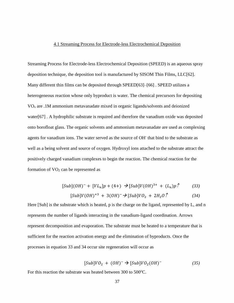
4.1 Streaming Process for Electrode-less Electrochemical Deposition
Streaming Process for Electrode-less Electrochemical Deposition (SPEED) is an aqueous spray
deposition technique, the deposition tool is manufactured by SISOM Thin Films, LLC[62].
Many different thin films can be deposited through SPEED[63]–[66] . SPEED utilizes a
heterogeneous reaction whose only byproduct is water. The chemical precursors for depositing
VOx are .1M ammonium metavanadate mixed in organic ligands/solvents and deionized
water[67] . A hydrophilic substrate is required and therefore the vanadium oxide was deposited
onto borofloat glass. The organic solvents and ammonium metavanadate are used as complexing
agents for vanadium ions. The water served as the source of OH- that bind to the substrate as
well as a being solvent and source of oxygen. Hydroxyl ions attached to the substrate attract the
positively charged vanadium complexes to begin the reaction. The chemical reaction for the
formation of VO2 can be represented as
[𝑆𝑢𝑏](𝑂𝐻)− + [𝑉𝐿𝑛]𝑝 + (4+) → [𝑆𝑢𝑏]𝑉(𝑂𝐻)3+ + (𝐿𝑛)𝑝 (33)
[𝑆𝑢𝑏]𝑉(𝑂𝐻)+3 + 3(𝑂𝐻)−→ [𝑆𝑢𝑏]𝑉𝑂2 + 2𝐻2𝑂 (34)
Here [Sub] is the substrate which is heated, p is the charge on the ligand, represented by L, and n
represents the number of ligands interacting in the vanadium-ligand coordination. Arrows
represent decomposition and evaporation. The substrate must be heated to a temperature that is
sufficient for the reaction activation energy and the elimination of byproducts. Once the
processes in equation 33 and 34 occur site regeneration will occur as
[𝑆𝑢𝑏]𝑉𝑂2 + (𝑂𝐻)− → [𝑆𝑢𝑏]𝑉𝑂2(𝑂𝐻)− (35)
For this reaction the substrate was heated between 300 to 500oC.

38
This method of deposition requires multiple spray cycles to build up thickness. In between these
cycles there is a relaxation time in order for the reaction between the chemicals to occur (up to 1
min). The relaxation periods length was found to affect the composition of the thin film and will
be discussed in section 4.4.
SPEED does not allow for accurate thickness control. Due to the nature of the of spray films,
growth does not occur evenly across the whole sample. Across our vanadium oxide sample the
thickness range was from .6 to 2µm. This unevenness will lead to changes in sheet resistance
throughout the sample and therefore differences in the electro-thermal properties of the material.
4.2 Visual Characterization
The first phase of characterization was optical visual characterization of the samples. Vanadium
oxide has different stable oxidation states, mainly VO2, V2O5 and V4O9. The VOx that is useful
for bolometers is that which has an x~2. This is due to VO2’s strong phase transition around
68oC, resistivity is shown to drop by orders of magnitude as this transition happens. The VOx
used in bolometers exhibits the strong TCR of VO2 before its transition but does not exhibit the
actual transition itself. This is extremely useful as the phase transition in VO2 is a non-linear
hysteresis effect which makes it undesirable for being able to measure temperature accurately as
its’ TCR is not linear. In VOx however, since there is no phase transition, and as such has a linear
TCR.
Although VO2 and V4O9 can be hard to distinguish visually V2O5 is easy to distinguish. While
the former oxidation states exhibit a dark grey to black-color when thick, the latter normally has

39
a bright saffron yellow color [68]. This is also important as V2O5 is a known carcinogen and
toxin if inhaled. The visual characterization gave us a good idea of what samples had higher
amounts of V2O5 in them. Figure 11 presents an image of 5 different SPEED deposited VOx
samples. From right to left the color of the samples changes from a dark grey to a yellow
indicative of vanadium pentoxide. While the samples did have different post-deposition
annealing conditions the formation of the yellow color was seen prior to this. Table 1 shows the
post-deposition anneal done to different samples as well as the visual color that was noted after
processing was done. From table 1 as well as knowing the yellow color appeared before post-
deposition annealing it can be inferred that post-deposition anneal has little to no effect on the
visual characteristics of the sample. As mentioned early there is a relaxation time in between
spray cycles. It was observed that if this relaxation time was too long a yellowish color would
appear, the sample had oxidized to too high of a state. It can be concluded that the oxidation state
of the sample is influenced more by the spray cycle time than the post-deposition annealing
process.
Table 1 shows the post-deposition annel done to different samples as well as the visual color that
was noted after processing was done
Figure 11 SPEED deposited VOx samples done with different post deposition processing

40
4.3 SEM/AFM
SEM and AFM data was collected in order to characterize the surface roughness of the films to
see if the surface features would be on the same order of magnitude and therefore interact with
the incident radiance. Figure 8 present an SEM image of a SPEED deposited VOx sample.
Images show a ropy-like structure interconnected throughout the surface and was indicative of
all the samples imaged. Previously SPEED deposited TiO2 exhibited a similar surface
morphology[69]. Further studies and refinements of theTiO2 SPEED deposition technique
showed that it was possible to create a smoother TiO2 surface, meaning in principle it should be
possible to get smoother morphology for vanadium oxide by SPEED[70]. The ropy structures
were around 2-5 microns in width and were seen over the whole sample.

41
Figure 12 SEM image of SPEED deposited VOx sample 3
Figure 9 displays an AFM image of the same VOx sample in figure 12. The surface roughness of
the sample was measured to be on average 60 nm, which is similar to other VO2 films[71]. No
major defects were seen in the AFM images. The surface roughness value is much less than the
infrared wavelengths being looked at for this application and therefore no significant effect on
the optical properties of the device would be expected.

42
Figure 13 AFM image of SPEED deposited VOx sample 3
4.4 X-ray Diffraction
Asymmetric out-of-plane X-ray diffraction was performed on the samples to help determine the
phase and stoichiometry of the VOx. Figure 10 shows the results of this x-ray diffraction on 3
samples. The curves represent the intensity of the scattering and the symbols with drop lines
represent reference data. Sample VOx-1 (black trace) seems to be comprised of mainly V2O5.
VO2 peaks start to be seen in samples VOx-2 (red trace) and VOx 3 (blue trace). VOx-2 also
exhibits peaks representative of V4O9. From this it is determined that a longer time spent in air
while heated either during deposition or in post-anneal heating resulted in a higher oxidation
state.

43
Figure 14 XRD data of SPEED deposited VOx films
4.5 TCR measurements
4-point probe method was used to evaluate the VOx films for their TCR. This method utilizes 4
probes that are known distances apart, either voltage or current is supplied by the outer probes
while the other is measured on the inner probes. Temperature dependent resistance
measurements were performed utilizing a substrate heater and a 4-point probe. Using this data in
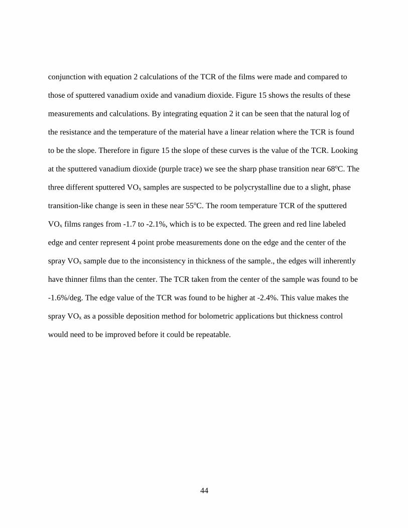
44
conjunction with equation 2 calculations of the TCR of the films were made and compared to
those of sputtered vanadium oxide and vanadium dioxide. Figure 15 shows the results of these
measurements and calculations. By integrating equation 2 it can be seen that the natural log of
the resistance and the temperature of the material have a linear relation where the TCR is found
to be the slope. Therefore in figure 15 the slope of these curves is the value of the TCR. Looking
at the sputtered vanadium dioxide (purple trace) we see the sharp phase transition near 68oC. The
three different sputtered VOx samples are suspected to be polycrystalline due to a slight, phase
transition-like change is seen in these near 55oC. The room temperature TCR of the sputtered
VOx films ranges from -1.7 to -2.1%, which is to be expected. The green and red line labeled
edge and center represent 4 point probe measurements done on the edge and the center of the
spray VOx sample due to the inconsistency in thickness of the sample., the edges will inherently
have thinner films than the center. The TCR taken from the center of the sample was found to be
-1.6%/deg. The edge value of the TCR was found to be higher at -2.4%. This value makes the
spray VOx as a possible deposition method for bolometric applications but thickness control
would need to be improved before it could be repeatable.

45
Figure 15 Plot of the natural log of the sheet resistance vs temperature for different VOx films
4.6 Summary
One of the objectives of this work is to make a repeatable, affordable, and efficient device.
Vanadium oxide is a common bolometric material. In order to make the most efficient bolometer
possible a novel deposition method, SPEED, was characterized against the most common
deposition method, sputtering.

46
SPEED deposited VOx was characterized by both SEM and AFM. SEM images showed a ropy
like surface structure. AFM images showed no significant features that would give rise to optical
problems in the LW or MWIR.
X-ray diffraction was performed on different SPEED deposited vanadium oxide samples to
determine the crystalline phase mixture present in the sample. Annealing temperatures and
environments of the SPEED deposited samples were studied for their effect on the overall film
composition. The relaxation time between sprays during deposition as well as the amount of time
post-annealed in air lead to higher oxidation states (V2O5 and V4O9) being present in the
samples. Future studies of this deposition method should look at the effect of depositing in a
reduced environment, as well as optimizing the spray time to better control the phase mixture
present.
The TCR, sheet resistance and resistivity for the films was characterized and compared to that of
conventionally sputter VOx. TCR of SPEED VOx was comparable of that to the sputtered
version. The TCR was found to be near the same as that of the sputtered version, though due to
the thickness gradient across the sample the TCR of the SPEED sample’s TCR was not uniform.
The edge of the sample exhibited extremely high TCR while the middle exhibited a
comparatively low TCR. Table 1 provides an overview of the visual and electrical
characterization done to the samples studied.
Due to the inability to accurately control thickness, and the difficulty in controlling oxidation
state the VOx chosen to be most suitable for this research’s application is conventionally

47
sputtered VOx though SPEED deposited VOx shows promising characteristics for use in other
infrared detectors.
Table 1 Characteristics of VOx Samples grown by SPEED
Sample # Post
Deposition
Anneal
Color Room
Temperature
Sheet
Resistance
(Ω/sq)
TCR
(%/oC)
Resistivity
(Ω-cm)
1 60 min 400
C in air
yellowish 9.2E+08 -2 100000
2 30 min 400
C in air
Mostly
gray, slight
yellow in
areas
1.7E+07 -2.2 19000
3 30 min 450C
in N2
Dark gray 6.6E+04 -2.4 5.9
4 None Uniformly
black
2.6E+07 -4 1600
5 30 min 450
C N2
Uniformly
yellow
8.8E+07 Not tested
due to
pentoxide
formation
1800

48
CHAPTER FIVE: BOLOMETER FABRICATION AND INTEGRATION
INTO MIM
Integration of absorbers into bolometers has been done many times before [72]. Previous work
done has integrated very similar type of absorber devices but in that work the device was placed
on top of the bolometer and lead to higher thermal mass of the bolometer and therefore higher
response time [73]. The goal of this work is to integrate the bolometer into the MIM device itself
by putting the bolometric material in the middle of the dielectric layer of the absorber therefore
reducing the amount of thermal mass added to the device.
5.1 Index of Material of Thin Film Stack
The first concern with integrating the VOx into the MIM device was its’ effect on the resonance
wavelengths. Eq 30 shows that the only material dependence on the resonance will be the index
of material of the dielectric.
Because fabrication of and integration were done in parallel with studies into the MIMs seen in
chapter four initially studies on the index of the thin film stack were done with SiO2 and not
AlN. Thin film stacks of SiO2/VOx/SiO2 were fabricated for testing. The initial substrate was a
thermally oxidized wafer with a nominal thickness of 1µm, the VOx was deposited through
pulsed laser deposition at 550oC. The top layer of SiO2 was deposited through plasma enhanced
chemical vapor deposition (PECVD) with a nominal thickness of 650nm. Ellipsometry was
performed using a Woolam IR-VASE ellipsometer. Measurements were taken from 1-15 µm,

49
measurements were taken on the initial thermally oxidized wafer as well as taken after each
subsequent deposition and the optical constants found at each of these steps. The thickness and
complex permittivity of each layer were found by fitting the ellipsometry data to a model for
every layer. For both materials the model used Gaussian oscillator terms (peak amplitude, energy
and broadening), for the VOx only a Drude term was added (amplitude and energy). Another way
to fit the data was for the program to treat the stack as an effective layer, similar to effective
medium theory mentioned earlier, in this the software does not make any type of analytical
model like it does when fitting individual layers.
Figure 16 presents the results of the ellipsometry data. In both of the plots all three different
layers (thermal SiO2, VOx and PECV SiO2) individual constants are compared to the constants
found using the effective medium. It can be noted that there are differences in the optical
constants between the two different SiO2 deposition methods. The index of PECVD oxide lower
magnitude peaks than that of thermally deposited silicon dioxide. The intrinsic absorption band
of SiO2 around 9 µm is offset by a half micron between the thermal and PECVD oxides. When
we compare the VOx constants to those of the SiO2 and effective constants we see a large
difference. The VOx seems to have no effect on the effective constants. The effective constants
are in between the PECVD and thermal oxide constants indicating the VOx will not change the
index of refraction and therefore not change the resonances in SiO2 based MIMs

50
Figure 16 Refractive index and extinction coefficients obtained through ellipsometry for
SiO2/VOx/SiO2 thin film stacks.
Although the VOx was found not to affect the optical constants of the SiO2 stack, once the
dielectric was chose to be AlN, the same verification had to made for it. Samples of AlN were
fabricated with a layer of VOx in the middle.IR ellipsometry was again used to find the index of
refraction of this AlN/VOx/AlN stack, and was compared to known crystalline AlN values.
Figure 17 (left) shows the results obtained from the IR ellipsometer. On the left the complex and

51
real parts of the index of refraction for a stack of AlN/VOx/AlN, the right image shows the
refractive index of AlN taken from literature. Comparing the two spectra it is clear that both
correspond extremely well to each other. The literature value has a dip near 11 microns in the
real part which is similar to the fabricated stack which also dips around 11 microns. While the
literature values have a smoother curve, the difference between these two indexes should not
have a noticeable effect in the calculation of the resonant wavelengths using equation 30. Due to
this we proceeded with integrating the VOx in the middle of the dielectric layer of the bolometer.
Figure 17(left) complex and real values of the index of refraction of an AlN/VOx/AlN thin-film
stack, taken with IR ellipsometry. (right) complex and real values of the index of refraction of
AlN
5.2 Bolometer Fabrication Process and Consideration
The fabrication and optimization of the processes was done throughout the entirety of the
project. The bolometer itself is based off of a design used before, the time was spent into
adapting the process to work with the materials being used.

52
The general process of the bolometer fabrication is a mostly bottom up procedure utilizing
photolithography and liftoff though some etch back steps were employed. After the devices were
built they were subsequently released through a plasma etch of the silicon substrate to undercut
the device.
5.2.1 Bolometer Fabrication Techniques
The techniques and tools employed throughout the fabrication. On every single layer an opening,
or “via” is left in the same spot around the bolometric elements. This will leave the pathway to
the silicon through which the undercut of the device will be done.
The first layer deposited is the bottom ground layer of the device. For this a bilayer of negative
photolithography utilizing lift off resist (LOR) under a negative tone resist was patterned leaving
only the vias to the silicon open. Ti or Al was deposited via e-beam deposition method onto this
wafer and then lifted off into a sonicator. This same procedure was done again except instead of
evaporating Ti on to the wafer AlN was reactively sputtered onto the substrate and subsequently
lifted-off in a sonicator. This dual-layer photolithography process is utilized in most layers.
The next layer deposited is the interconnects. These go from the bolometric element to large
bond pads which can be wire bonded to. These interconnects are what will be used to connect the
devices to circuitry. This layer was initially done utilizing a similar bilayer resist as the last, but
in this case nickel was the material used as the interconnect metal.
Once the interconnects are deposited the next step is to deposit and pattern the VOx. To do this
an etch back of the VOx was done due to restraints of the sputtering system used for the

53
vanadium oxide depositions. VOx was blank sputtered over the entire wafer. After this a positive
tone resist was spun onto the wafer and patterned leaving photoresist only over the active
bolometer areas themselves. This photoresist will act as a protectant mask during the VOx etch
back. Once the photoresist layer has been patterned and developed the wafer is put into an RIE
etcher. It undergoes a plasma etch utilizing SF6 at 150W RIE power. The plasma etch will etch
away all of the vanadium oxide very quickly (<2min) but will not etch away the photoresist in
that time. After this an O2 plasma clean utilizing a desktop RIE system is used to remove the
photoresist.
The next step in the fabrication is putting down the top layer of AlN. To do this just as with the
first layer a bi-layer of lift off resist/negative tone resist is utilized. The photoresist is patterned in
such a way that the photoresist is left where the vias to the silicon are located as well as where
the bond pads for the interconnects are. After this AlN is sputtered onto the sample and lifted off
in a sonicator.
At this point in the fabrication this device is a bolometer. The last step of the device is to put the
gold square array on top of the bolometric elements. To do this a dual layer of LOR/positive-tone
resists was used. The square arrays were patterned onto the resist utilizing photolithography and
then gold was e-beam evaporated and then lifted off in a sonicator. The squares are now covering
the entire wafer, but they are only needed on the bolometers, having them on the whole surface
would create problems for heat transfer as the whole wafer would then be acting as an absorber.
To remove the unwanted squares an etch back technique similar to that used for the VOx is
employed. Positive photoresist is patterened so that it covers the bolometric elements (and the

54
squares on top). The substrate is then placed into a wet gold etchant for 5 minutes. After which
the gold will be removed everywhere except where the photoresist was covering. An O2 plasma
clean is done to remove the resist.
The last deposition is the bond pads. The bi-layer LOR/negative resist is used and the bond pad
design is patterned into the resist. Gold is e-beam evaporated onto the sample and then lifted off.
At this point the last step of the process is undercutting the devices. The bolometric elements and
its squares are protected utilizing positive photoresist. The silicon is undercut utilizing a
fluorinated plasma in a barrel asher RIE system. This process as well as all the others and the
process leading to those processes will be explained in detail in subsequent sections.
5.3 MIMs-Bolometer-Integration process
The process of going from a normal bolometer process to integrating the MIMS devices was an
arduous process. The first step was finding a way to pattern the needed materials for the MIM
part of the device, i.e. Al or Ti and AlN. The former worked using simple single layer resist
photolithography. The AlN however had many problems becoming compatible with the
fabrication process. The sputtered AlN was extremely difficult to liftoff using single-layer
photolithography. This problem was determined to be from the deposition method itself.
Sputtering, unlike e-beam or thermal evaporation, is not a directional process, the ions have any
number of velocity vectors. Due to this the coatings from sputtering are more conformal than
those of more directional deposition methods. In photolithography this can cause problems as a

55
perfectly conformal film; with no breaks anywhere; leaves no openings for the solvents to
permeate through and even if it did the AlN would not lift off as it would still be connected to the
bulk material.
The first solution implemented for this problem was to try doing a top-down procedure for this
step by using KOH to etch the AlN. In order to do this a hard mask was employed to protect the
rest of the AlN. Normal positive photoresist was employed at first to try to act as a hard mask but
unsurprisingly the dissolution rate of the resist was similar if not higher to that of the AlN in
KOH leading to the AlN that needed to be protected becoming damaged in the etch process. To
try and remedy this SU-8 was employed as a hard mask. Figure 18 (left) shows an optical
microscope image of a sample of AlN on silicon that utilized normal photoresist as a hard mask
and KOH to etch back the AlN. The purple substance is the surviving photo resist mask. The
mask that is remaining is damaged and pock marked. The grey/white areas are vias to the
silicon. The orange bands are AlN that has started to be etched away, the edges are eroded and
angled. Figure 18 (right) displays an optical microscope image of an alignment marker of one of
the patterns. The purple iridescent area is AlN that has SU-8 on top as a hard mask. The
white/grey rectangle in the middle is exposed silicon. The thin strip of grey between the
iridescent area and the silicon is SU-8 that has no AlN underneath it as the AlN has been etched
by the KOH there.
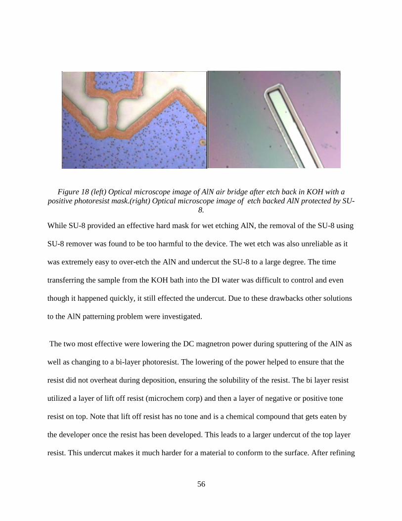
56
Figure 18 (left) Optical microscope image of AlN air bridge after etch back in KOH with a
positive photoresist mask.(right) Optical microscope image of etch backed AlN protected by SU-
8.
While SU-8 provided an effective hard mask for wet etching AlN, the removal of the SU-8 using
SU-8 remover was found to be too harmful to the device. The wet etch was also unreliable as it
was extremely easy to over-etch the AlN and undercut the SU-8 to a large degree. The time
transferring the sample from the KOH bath into the DI water was difficult to control and even
though it happened quickly, it still effected the undercut. Due to these drawbacks other solutions
to the AlN patterning problem were investigated.
The two most effective were lowering the DC magnetron power during sputtering of the AlN as
well as changing to a bi-layer photoresist. The lowering of the power helped to ensure that the
resist did not overheat during deposition, ensuring the solubility of the resist. The bi layer resist
utilized a layer of lift off resist (microchem corp) and then a layer of negative or positive tone
resist on top. Note that lift off resist has no tone and is a chemical compound that gets eaten by
the developer once the resist has been developed. This leads to a larger undercut of the top layer
resist. This undercut makes it much harder for a material to conform to the surface. After refining

57
the process this dual layer resist lead to the quickest and most reliable way to lift off the
sputtered AlN.
Once the AlN liftoff procedure had been solved, undercutting of the material needed to be
proved possible. When looking at undercutting the bolometer the process has to etch silicon at a
rapid rate as the bolometer is 40 microns in width meaning that from each side 20 microns
needed to be isotopically etched. Fluorinated plasma etching in a barrel asher was utilized. The
barrel asher provides an isotropic etch by having no directionality and completely random
velocity vectors of the ions.
5.3.1 VOx Process Integration
VOx deposition and patterning is the next step in fabrication. As stated earlier the VOx utilized in
these devices is sputtered. The sputtering is done in an AJA Phase II. Reactive RF sputtering
from a pure V target in a .2% O2 in Ar gas mixture, the substrate is heated to 400oC during
deposition.
The high temperatures meant that most photoresists will burn during this deposition. This
constraint led to a top down approach for patterning being utilized. First VOx is blanket sputtered
over the whole substrate. The bolometric areas of the sample are then masked by patterning
photoresist over the bolometric areas. A fluorinated plasma etch is utilized to etch the exposed
VOx. The plasma etch was done in a RIE plasma etcher utilizing a pure SF6 environment and a
power of 150W, CF4 was also shown to work but was more damaging to the AlN on the sample

58
as well as being a slower etch for the VOx The photoresist mask is removed utilizing an O2
plasma clean .Figure 19 is an optical microscope image of an AlN based bolometer sample after
VOx has been deposited and patterned. The light yellow areas that cover most of the picture is
titanium underneath a layer of AlN The darker gold areas are the interconnects which provide
electrical connections from the device itself out to bond pads which can then be wired bonded to.
The blueish-gray x-shaped areas are the silicon vias through which the bolometer itself will
eventually be undercut. The square green area in between the end of the interconnects it the
patterned vanadium oxide. The area on which this vanadium oxide resides is known as the
bolometric area.
Figure 19 Optical microscope image of AlN based bolometer after VOx has been deposited and
fabricated

59
Capping the VOx with the next AlN is done quickly after the VOx patterning to ensure the VOx is
protected and does not have the possibility of oxidizing further.
5.3.2 Top Metal Integration
Integrating the metal squares into the process was simple enough. Mask constraints meant that an
etch back would be necessary for the patterning of squares. Squares of different sizes were
patterned in 1” by 1” arrays over the substrate using bi-layer photolithography.
Gold was e-beam evaporated onto the wafer and subsequently lifted off. Once the gold squares
were deposited, a protective coating of photoresist was patterned and developed over the
bolometric areas on the wafer, protecting the squares just like the VOx was protected. The
substrate is then submerged in gold etchant type TFA for 5 min. After which the gold squares not
protected will have been removed and an O2 plasma clean is once again utilized to get rid of the
photoresist. Figure 20 shows images of a sample before(top) and after (bottom) having the gold
squares etched back. In the top image an array of squares over the whole surface can be seen.
The bototm image shows the sample after utilizing the photoresist mask and etch back
procedure. Here the gold squares can only be seen on the bolometric area of the sample. Note
that the difference in square size is due to these bolometers being at different areas of the same
wafer.

60
Figure 20 (top) AlN based bolometer with gold squares coating entire surface before au etch
back (bottom) same sample after gold etch back.
5.3.3 Undercut with MIMs
Although the undercut had already been established for AlN problems arose when trying to
undercut after the squares had been deposited. Initial undercuts showed that the gold squares
were being removed during the fluorinated process. Pulse depositions were done to limit heating

61
of the substrate, au was still shown to be removed indicating the removal was not due to thermal
processes. The removal could be due to physical interaction, this could be tested by using a lower
power for the etch, this was not possible in our system as the minimum power possible was
400W.
The solution implemented for this problem was the same done for VOx and the gold squares.
Photoresist was used as a protective mask over the bolometric areas during undercut. The
photoresist used was S1813 (microchem corp.) and a post develop bake of 115oC for 5 min was
done to harden the resist to make it more etch resistant. Once the undercut is done the photoresist
is removed with O2. This method showed no damage done to the squares
Figure 21 displays an SEM image of a bolometer with the photoresist mask covering the squares.
The blurriness of the squares is due to this photoresist layer. The dark black areas around the
bolometric area are the areas which will be undercut.

62
Figure 21 SEM image of a bolometer with the gold squares coated in protective photoresist prior
to being undercut
Figure 22 presents two SEM images, one showing an array (left) and one showing a single pixel
of an AlN-MIM integrated bolometer array. This array has been undercut and the protective
layer of photoresist removed. Comparing both images in figure 22 to 21 it is apparent that the
squares are not as blurry in figure 22 due to the removal of the resist. The left image shows that
all of the bolometers in the array were similarly undercut and free standing while the right image
shows the full detachment of a single bolometer. In the right image the dark bump underneath
the pixel is the silicon substrate left after the undercut procedure.

63
Figure 22(left) SEM image at x800 of AlN MIM integrated bolometer array. (right) SEM image
at x3.5k of a single AlN MIM integrated bolometer showing full suspension from the substrate

64
CHAPTER SIX: BOLOMETER CHARACTERIZATION
6.1 Experimental Methods
Characterization of the bolometer was done using a typical black-body setup. The black-body
source used was a tube furnace with one end plugged using a piece of firebrick and a 1” aperture
at the other end. The measurements taken were done at temperatures from 0 oC -1200oC. The
distance from the aperture to the bolometer was 7.8”. Radiation from the black body was
modulated using an optical chopper from 10-2000Hz.
Detectors were mounted onto a ceramic chip carrier and aluminum wire was used to wire bond
the bond pads of the device to those of the chip carrier. The chip carrier was mounted into a
socket that had been soldered to a printed circuit board (PCB). Figure 23 (left) shows an example
of one AlN-MIM integrated bolometer mounted into a ceramic chip carrier. The two white lines
horizontally oriented on the sample are the bolometer arrays. The aluminum wires can be seen
going from the samples bond pads to the chip carrier pads. Figure 23 right shows an example of
a ceramic chip carrier mounted into a socket. The PCB allows for electrical connections to be
routed to characterization equipment.

65
Figure 23 (left) Photograph of an AlN-MIMs integrated bolometer die mounted and wire bonded
to a ceramic chip carrier (right) photograph of an AlN-MIMs integrated bolometer on a chip
carrier mounted in a socket on a PCB
The PCB was mounted into a vacuum box with electrical feed through and a KRS-5 (thallium
bromo-iodide) window with transmission of ~70% within 0.6-40 µm wavelength. Measurements
were done with the box at ~60mT.
As stated earlier the bolometer is put in series with a load resistor as shown in Figure 1. The load
resistor and bolometer were chosen to be impedance matched for equations 22-26 to remain
valid. A DC-voltage power supply was utilized as the bias voltage. The bias voltage applied to
devices was optimized by looking at bias voltages effect on response voltage. The optimized bias
voltage ranged from 3-6V depending on the bolometer. Change in Vout due to modulation of the
power source (blackbody) was amplified using a lock-in amplifier (Stanford Research Systems
SR540 analog), the reference for the lock-in was taken from the optical chopper controller. Noise
was measured separately utilizing an HP spectrum analyzer, with no power incident on the
detector other than background radiation. The data was output through a lab-view program, noise
was taken from 0-100kHz.

66
Figure 24 shows a top-down photograph of the experimental setup used. The tube-furnace black
body is at the left of the picture. The large silver box at the top center of the picture is the
vacuum box in which the sample is held, the sample is located at the lower left side of the box in
this picture approximately 2 cm from the left side wall. An optical chopper can be seen just left
of the lower part vacuum box where the sample is held. In the bottom right a breadboard can be
seen, this breadboard is where the load resistor circuit is held. The grey BNC cable going from
the vacuum box to the resistor circuit provides connection into the vacuum box and to the sample
being measured.
Figure 24 Top-down photograph of experimental setup for bolometer characterization.

67
6.2 Measurements
6.2.1 Noise Measurements
Before looking at the noise measurements it is pertinent to quickly go over two types of noise.
1/f noise and Johnson noise. 1/f noise is named due to its dependence on frequency. This noise is
poorly understood but is related to fluctuations in the resistance of the material. The noise has
also been shown to be material dependent with different deposition techniques, dimensions and
materials affecting the noise. Electrical contacts of the device have been shown to play
significant roles in 1/f noise [74]. Particularly non-ohmic contacts have been shown to affect 1/f
noise.
Unlike 1/f noise Johnson noise is quite well understood and is not frequency dependent. Johnson
noise arises from fluctuations in the resistance across the material. These resistance fluctuations
derive from the fluctuations in charge carriers’ thermal motion within the material. This change
in resistance will lead to changes in potential across the resistor. The mean RMS fluctuations
from Johnson noise can be written as[46]
𝛿𝑉𝑗 = √4𝑘𝐵𝑇𝑅∆𝑓 (36)
where kB is Boltzmanns’ constants, T is the temperature of the device, R is the resistance of the
device and ∆f is the electronic measurement bandwidth. Cooling the device is an effective way to
reduce Johnson noise. For uncooled detectors like ours Johnson noise can be reduced only
through lowering the resistance of the detector.
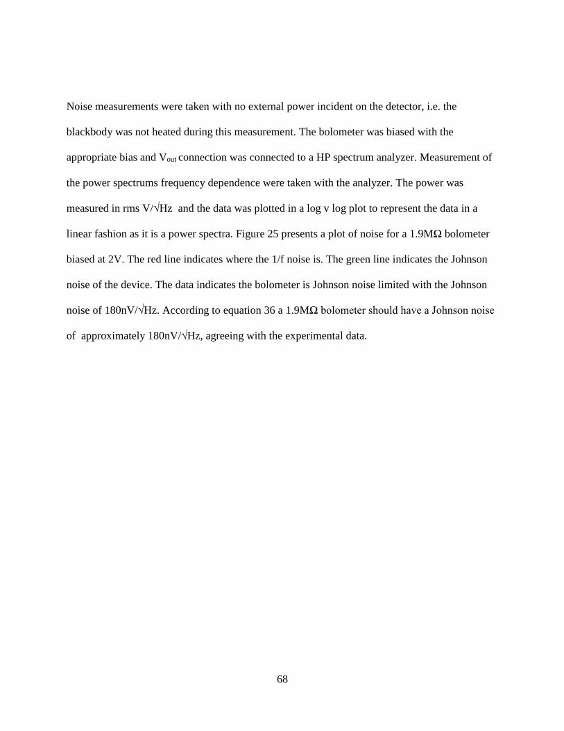
68
Noise measurements were taken with no external power incident on the detector, i.e. the
blackbody was not heated during this measurement. The bolometer was biased with the
appropriate bias and Vout connection was connected to a HP spectrum analyzer. Measurement of
the power spectrums frequency dependence were taken with the analyzer. The power was
measured in rms V/√Hz and the data was plotted in a log v log plot to represent the data in a
linear fashion as it is a power spectra. Figure 25 presents a plot of noise for a 1.9MΩ bolometer
biased at 2V. The red line indicates where the 1/f noise is. The green line indicates the Johnson
noise of the device. The data indicates the bolometer is Johnson noise limited with the Johnson
noise of 180nV/√Hz. According to equation 36 a 1.9MΩ bolometer should have a Johnson noise
of approximately 180nV/√Hz, agreeing with the experimental data.

69
Figure 25 Noise of a 180MΩ bolometer biased at 2V.
6.2.2 Incident Power
Knowing the incident radiant power on the bolometer is imperative to calculate responsivity
through eq 19. This power can be calculated by looking at the radiance of a blackbody given by
𝐿 =𝜎𝑇4
𝜋 (37)
0.01 0.1 1 10 1001E-8
1E-7
1E-6
1E-5
1E-4
Ga
in C
orr
ecte
d N
ois
e (
V/
Hz)
Frequency (kHz)
f -1 180 nV/Sqrt Hz

70
This is found by integrating the radiance of an object over all wavelengths. T is the temperature
of the black body and σ is the Stefan-Boltzmann constant. This form of radiance is power per
unit source area per unit solid angle. Solid angle is defined by
𝛺 =𝐴𝑑
𝑟2 (38)
Where Ad is the area of the device upon which the radiation is incident and r is the distance of
the device from the black body aperture. For our devices the active bolometric area is 1.6x10⁻⁵
cm2.
The black body itself can be looked at as a collection of point sources. Each of these point
sources will emit the same power onto the detector as their solid angles will all be identical.
Total power on the device is just the integration over the area of the blackbody, giving
𝑃 = 𝐿 × 𝛺 × 𝐴𝐵𝐵 (39)
Where ABB is the surface area of the black body source. Eq 39 does not however account for the
KRS-5 window and its’ transmission. The responsivity measurements are taken at a temperature
such that the background radiance can be neglected and the radiance of the black body. With this
the power on the detector is
𝑃 = 𝐿 × 𝛺 × 𝐴𝐵𝐵 × 𝑇𝐾𝑅𝑆−5 (40)
Where 𝑇𝐾𝑅𝑆−5 is the transmission of the KRS-5 window, which is ~70% from .6-40 µm.

71
6.2.3 Responsivity measurements
Responsivity measurements were taken using the black-body set-up. Two types of response were
measured with this setup, bias voltage response and frequency response. Frequency response was
measured by recording response voltage as a function of frequency, 60Hz frequency and
multiples of it were avoided in order to minimize 60Hz noise in the measurements. Above 200Hz
a voltage amplifier was used to filter out frequencies lower than 100Hz
Figure 26 presents a plot of the frequency response of a 1.9MΩ MIMs integrated bolometer. The
data was taken using a constant bias voltage of 3V. The thermal time-constant was derived by
taking the voltage response given by Eq 26, and rewriting it as
𝑅𝑣 =𝑅𝑜
√1+(2𝜋𝑓)2(𝜏𝑡ℎ)2 (37)
Where 𝑅𝑜 =𝑉𝑏∝𝜂
4𝐺 represents the response at 0 Hz frequency. By fitting this equation to the
response curve in OriginPro software and making Ro and τth as parameters the thermal time
constant can be found. In figure 26 this fit is shown as the red curve, with the experimental data
being the black trace. Thermal time constant of this 1.9MΩ bolometer was found to be 4.6 ms,
which was similar for all bolometers measured.
Once the thermal time constant is found the effective thermal conductance can be found by using
eq. 18. The heat capacity of the device was found using Dulong-Petit Law. Through this the heat
capacity of many solid elements can be estimated to be 25 J/molK [75]. Using this model and
knowing the geometry and dimensions of the different thin films calculating the heat capacity is

72
simple. The thermal conductance found using this method was Geff= 1.7x10⁻⁸ W/K for a 1.9MΩ
bolometer.
Figure 26 Frequency Response of a 1.9MΩ bolometer
Responsivity was determined by taking response measurements at varying temperatures, as
shown in figure 27. This plot shows the responsivity of a 1.9MΩ bolometer. Measurements were
taken with a bias voltage of 2V and a chopping frequency of 36Hz. Measurements were taken
every 15 degrees. Utilizing equation 40 to calculate the power incident on the detector, and the
data in figure 27 the responsivity was found to be 𝑅𝑣 = 560𝑉
𝑊.
0 200 400 600 800 10000
4
8
Photo
respo
nse
(m
V)
Frequency (Hz)
1/ = 217 Hz
= 4.6 ms

73
500 600 700 800 9000
5
10
Experiment
Photo
respo
nse (
mV
)
Blackbody temperature (oC)
Figure 27 Plot of blackbody temperature vs photo-response for a 1.9MΩ bolometer
The effect of bias voltage was studied and compared to the voltage dependence of Eq. 23. Figure
28 presents experimental data in black with the red line representing a linear fit to the data. In
this experiment the blackbody temperature was at 830oC with a chopping frequency of 36Hz.
The bias voltage according to eq. 23 should have a linear effect on bias voltage, hence the linear
fit. Linear fit of the data shows agreement up until 3.5 V. This deviation can be due to noise
becoming more prevalent at higher bias. While not all noises are bias voltage dependent like
Johnson noise, some are for instance joule heating of the device. This curve was used to

74
determine the ideal bias voltage to use for other response measurements. For this bolometer a
bias voltage of 2-3V was chosen for the remaining measurements that had to be taken.
0 2 4 60
10
20
30
Photo
respo
nse (
mV
)
Bias (V)
Figure 28 Photoresponse vs bias voltage. The effect shows a linear trend up to 3V.
Finding the best bias voltage is important as an excessive bias voltage can damage the device. A
high enough voltage can result in a complete breakdown of the resistive element, collapsing the
bolometer and creating an open circuit.

75
6.3 FOM and Discussion
Once response was calculated the figure of merits, NEP, and D*, were calculated. The
derivations of these FOM were done in chapter two section two. NEP was calculated through Eq.
27. Utilizing the data form section 6.2 the NEP of a 1.9MΩ MIM integrated absorber was
measured to be .32nW. Table 2 presents the sample conditions, characterization parameters, and
FOM for different bolometers. Looking at previous devices of similar geometry that were made
by putting the absorbers gave a time constant of 4.82ms, without absorbers these devices had a
time constant of 4.05ms. Comparing these to the values of our bolometers we see that we were
able to drop the time constant which is expected due to the reduction of thermal mass of the
integrated bolometers. The time constant could be possibly reduced further by studying materials
with a lower index of refraction in order for the dielectric layer to be thinner and therefore reduce
total thermal mass.
Table 2 Table of MIMs integrated bolometers geometrical and electrical characterization
parameters and their FOM
Sample
Conditions
AlN
Thickness
Sample
Resistance
[Ω]
Thermal
Time
Constant
[ms]
NEP[W] D*[Jones
MIM
integrated
bolometer,
35 Hz, 2V
~300 nm 1.9 x 10⁶ 4.62 3.2 x 10-
10
7.2 x 10⁷

76
CHAPTER SEVEN: CONCLUSIONS
7.1 Discussion
We have successfully integrated VOx bolometers into a MIM resonant absorber.
Metal-insulator-metal electromagnetic absorbers were fabricated. An analytical standing wave
model used to describe the absorptions within the MIMs was tested for validity within the LWIR
and MWIR. Results showed good agreeance between theory and experiment, small discrepancies
in the data stem from the deposition methods used and the slight differences in the index of
refraction of the material compared to its crystalline counterpart due to the polycrystalline or
amorphous phases theses deposition methods produce. Utilizing the standing-wave model
dispersion within the desired bandwidths of the dielectric used in the MIMs was investigated for
its effect on the devices’ resonant wave lengths. These dispersive features were found to lead to
multiple resonant harmonics within the range of interest. For a spectrally selective bolometer like
ours this is unwanted. Therefore four different dielectrics were studied for their effect on the
MIMs resonance and to find the ideal material for single resonance within the LWIR and MWIR.
Of those investigated (AlN, TiO2, SiO2, and SiN4) AlN was found to have the most ideal material
properties for a selective wavelength bolometer in the LWIR.
A novel aqueous spray deposition method of vanadium oxide; known as SPEED; was studied
for its’ validity as a bolometric material. The VOx was characterized by AFM, SEM, XRD and 4-
point probe. AFM and SEM were used to determine surface roughness, which was found to be of
a small enough magnitude that it would not interact with the IR wavelengths being used here.

77
XRD showed that all oxidations states of vanadium oxide could be formed depending on
condition. The dwell time in between sprays was shown to lead to higher oxidations states within
the films. Lastly 4-point probe measurements were done while the film was heated to measure
sheet resistance as a function of temperature. TCR of the SPEED deposited films was found
range from -1.6%/oC to -2.4%/oC. These values are comparable to sputtered VOx films TCR and
shows that SPEED deposited VOx is a good candidate for a bolometric material if thickness and
oxidation states can be better controlled
The MIMs integrated bolometers were fabricated and tested in a black body setup. Bolometers
were measured for their frequency, voltage, and temperature response. The noise of the
bolometer was measured and compared to theoretical calculations. From this data the thermal
time constant as well as other FOM (NEP, D*, responsivity) were calculated. The MIMs
integrated bolometers showed a responsivity of 560V/W, a NEP of .32nW and a D* value of
7.2x10⁷ Jones.
7.2 Future Optimization and Experiments
The main experiment that should be done on these sample in the future is spectral response
characterization. Spectral response measures a devices absorption dependence on wavelength.
This will show the wavelength selectivity of the bolometers themselves. Spectral response could
be done in two ways. The first is by using an FTIR spectrometer, putting the bolometer into the
spectrometer the signal of the bolometer can be routed outside of the cavum chamber and into a
custom interface box. This interface box’s output goes into the spectrometer as a detector. In this

78
way the bolometer is both the sample, and the detector of the spectrometer. The second method
is to utilize a tunable quantum cascade laser to characterize the spectral response of the
bolometer. This method has been used before for pyroelectric detectors
Future investigations into MIMs integrated bolometers could be improved. A phase-shift
photolithography mask or a similar solutions should be implemented for patterning the square
features for the top structures of the MIMs. This is to ensure more geometrically accurate squares
and less rounding of the corners which will lead to better agreeance with theory.
Material properties could be improved to yield a better, less noisy bolometer. The VOx
deposition method should be studied more intensively to investigate how to lower the resistance
of the VOx to lower the noise of the device.
Other improvements could be made to the experimental setup, for instance a zinc-selenide
window instead of a KRS-5 window, as a zinc selenide windows transmittance range is smaller,
but still includes the LWIR.

79
APPENDIX: MY PUBLICATIONS

80
1. S. R. Calhoun V. C. Lowry, R. Stack, R. N. Evans, J. R. Brescia., C. J. Fredricksen, J.
Nath, R. E. Peale, E. M. Smith, J. W. Cleary “Effect of dispersion on metal–insulator–
metal infrared absorption resonances,” MRS Communications, vol. 8, no. 3, pp. 830–834,
Sep. 2018.
2. S. Calhoun, R. Evans, C. Nickle, I. O. Oladeji, J. Cleary, E. M. Smith, S. Chandra, D.
Chanda, R. E. Peale., “Vanadium Oxide Thin Film by Aqueous Spray Deposition,” MRS
Advances, vol. 3, no. 45–46, pp. 2777–2782, ed 2018.
3. R. E. Peale, S. Calhoun, N. Dhakal, I. O. Oladeji, and F. J. González, “Spray-on
thermoelectric energy harvester,” MRS Advances, vol. 4, no. 15, pp. 851–855, 2019.
4. R. N. Evans, S. R. Calhoun, J. R. Brescia, J. W. Cleary, E. M. Smith, and R. E. Peale,
“Far-infrared bands in plasmonic metal-insulator-metal absorbers optimized for long-
wave infrared,” MRS Advances, vol. 4, no. 11–12, pp. 667–674, ed 2019.
5. S. Alhasan, S. R. Calhoun, H. Aboelkhair, V. C. Lowry, R. E. Peale, I. Rezadad, E. M.
Smith, J. W. Cleary, I. O. Oladeji., “Smooth TiO2 Thin Films Grown by Aqueous Spray
Deposition for Long-Wave Infrared Applications,” MRS Advances, vol. 3, pp. 1–6, Jan.
2018.
6. H. Abouelkhair, P. N. Figueiredo, S. R. Calhoun, C. J. Fredricksen, I. O. Oladeji, E. M.
Smith, J. W. Cleary, R. E. peale “Ternary lead-chalcogenide room-temperature mid-
wave infrared detectors grown by spray-deposition,” MRS Advances, vol. 3, pp. 1–7,
Feb. 2018.
7. R. N. Evans, S. R. Calhoun, J. R. Brescia, J. W. Cleary, E. M. Smith, and R. E. Peale,
“Far-infrared bands in plasmonic metal-insulator-metal absorbers optimized for long-
wave infrared,” MRS Advances, vol. 4, no. 11–12, pp. 667–674, ed 2019
8. R. E. Peale, S. Calhoun, C. J. Fredricksen, E. Smith, S. Vangala, K. Leedy, J. R.
Hendrickson, J. W. Cleary “Effect of Compound Dielectric and Metal Thinning on
Metal-Insulator-Metal Resonant Absorbers for Multispectral Infrared Air-Bridge
Bolometers,” MRS Advances, vol. 2, no. 42, pp. 2281–2286, 2017.
9. R. E. Peale, C. J. Fredricksen, A. V. Muraviev, D. Maukonen, H. M. Quddusi, S.
Calhoun, J. E. Colwell, T. A. Lachenmeier, R. G Dewey, A. Stern, S. Padilla, R. Bode,
“Planetary atmospheres minor species sensor balloon flight test to near space,”
Proceedings of SPIE - The International Society for Optical Engineering, vol. 9491,
May 2015.
10. C. J. Fredricksen, S. Calhoun, S. Trewick, A. Coffey, E. Dein, K. R. Coffey, R. E. Peale,
J. D. LaVeigne, G. Franks, T. Danielson, J. M. Lannon, S. H. Goodwin, “Test pixels for

81
high-temperature infrared scene projection,” in Infrared Imaging Systems: Design,
Analysis, Modeling, and Testing XXVI, 2015, vol. 9452, p. 94520X.

82
LIST OF REFRENCES
[1] F. Niklaus, C. Vieider, and H. Jakobsen, “MEMS-Based Uncooled Infrared
Bolometer Arrays–A Review,” Proc. SPIE - Int. Soc. Opt. Eng., vol. 6838, Mar.
2008.
[2] D. Nguyen, F. Simoens, J. Ouvrier-Buffet, J. Meilhan, and J. Coutaz, “Broadband
THz Uncooled Antenna-Coupled Microbolometer Array—Electromagnetic Design,
Simulations and Measurements,” IEEE Trans. Terahertz Sci. Technol., vol. 2, no. 3,
pp. 299–305, May 2012.
[3] B. Li, “Design and simulation of an uncooled double-cantilever microbolometer
with the potential for ∼mK NETD,” Sens. Actuators Phys., vol. 112, no. 2, pp. 351–
359, May 2004.
[4] M. Almasri, Bai Xu, and J. Castracane, “Amorphous silicon two-color
microbolometer for uncooled IR detection,” IEEE Sens. J., vol. 6, no. 2, pp. 293–
300, Apr. 2006.
[5] Aaron J. Miller, Arttu Luukanen, and Erich N. Grossman, “Micromachined antenna-
coupled uncooled microbolometers for terahertz imaging arrays,” presented at the
Proc.SPIE, 2004, vol. 5411.
[6] C. M. Travers, A. Jahanzeb, D. P. Butler, and Z. Celik-Butler, “Fabrication of
semiconducting YBaCuO surface-micromachined bolometer arrays,” J.
Microelectromechanical Syst., vol. 6, no. 3, pp. 271–276, Sep. 1997.
[7] D. P. Neikirk and D. B. Rutledge, “Air‐bridge microbolometer for far‐infrared
detection,” Appl. Phys. Lett., vol. 44, no. 2, pp. 153–155, Jan. 1984.
[8] J. P. Rice, E. N. Grossman, and D. A. Rudman, “Antenna‐coupled high‐ T c air‐
bridge microbolometer on silicon,” Appl. Phys. Lett., vol. 65, no. 6, pp. 773–775,
Aug. 1994.
[9] D. P. Neikirk, W. W. Lam, and D. B. Rutledge, “Far-infrared microbolometer
detectors,” Int. J. Infrared Millim. Waves, vol. 5, no. 3, pp. 245–278, Mar. 1984.
[10] R. A. Dunlap, Experimental physics: modern methods. New York: Oxford
University Press, 1988.
[11] A. Goyal et al., “Material characteristics of perovskite manganese oxide thin films
for bolometric applications,” Appl. Phys. Lett., vol. 71, no. 17, pp. 2535–2537, Oct.
1997.
[12] A. Y. Glamazda, V. A. Karachevtsev, W. B. Euler, and I. A. Levitsky, “Achieving
High Mid-IR Bolometric Responsivity for Anisotropic Composite Materials from
Carbon Nanotubes and Polymers,” Adv. Funct. Mater., vol. 22, no. 10, pp. 2177–
2186, 2012.
[13] J.-S. Shie and Y.-M. Chen, “Metal-Film Microbolometer,” J.
MICROELECTROMECHANICAL Syst., vol. 5, no. 4, p. 9, 1996.

83
[14] S. Sedky, P. Fiorini, M. Caymax, A. Verbist, and C. Baert, “IR bolometers made of
polycrystalline silicon germanium,” Sens. Actuators Phys., vol. 66, no. 1, pp. 193–
199, Apr. 1998.
[15] M. Pedretti et al., “Measurement of thermal properties for modeling and
optimization of large mass bolometers,” Phys. B Condens. Matter, vol. 329–333, pp.
1614–1615, May 2003.
[16] N. Fieldhouse, S. M. Pursel, M. W. Horn, and S. S. N. Bharadwaja, “Electrical
properties of vanadium oxide thin films for bolometer applications: processed by
pulse dc sputtering,” J. Phys. Appl. Phys., vol. 42, no. 5, p. 055408, Feb. 2009.
[17] R. T. Rajendra Kumar et al., “Pulsed laser deposited vanadium oxide thin films for
uncooled infrared detectors,” Sens. Actuators Phys., vol. 107, no. 1, pp. 62–67, Oct.
2003.
[18] B. Wang, J. Lai, H. Li, H. Hu, and S. Chen, “Nanostructured vanadium oxide thin
film with high TCR at room temperature for microbolometer,” Infrared Phys.
Technol., vol. 57, pp. 8–13, Mar. 2013.
[19] H. Wang, X. Yi, and S. Chen, “Low temperature fabrication of vanadium oxide
films for uncooled bolometric detectors,” Infrared Phys. Technol., vol. 47, no. 3, pp.
273–277, Jan. 2006.
[20] Y.-H. Han et al., “Fabrication of vanadium oxide thin film with high-temperature
coefficient of resistance using V2O5/V/V2O5 multi-layers for uncooled
microbolometers,” Thin Solid Films, vol. 425, no. 1, pp. 260–264, Feb. 2003.
[21] M. S. B. de Castro, C. L. Ferreira, and R. R. de Avillez, “Vanadium oxide thin films
produced by magnetron sputtering from a V2O5 target at room temperature,”
Infrared Phys. Technol., vol. 60, pp. 103–107, Sep. 2013.
[22] A. Zylbersztejn and N. F. Mott, “Metal-insulator transition in vanadium dioxide,”
Phys. Rev. B, vol. 11, no. 11, pp. 4383–4395, Jun. 1975.
[23] A. J. Syllaios, T. R. Schimert, R. W. Gooch, W. L. McCardel, B. A. Ritchey, and J.
H. Tregilgas, “Amorphous Silicon Microbolometer Technology,” MRS Proc., vol.
609, Jan. 2000.
[24] C. Vedel, J.-L. Martin, J.-L. Ouvrier-Buffet, J.-L. Tissot, M. Vilain, and J.-J. Yon,
“Amorphous-silicon-based uncooled microbolometer IRFPA,” in Infrared
Technology and Applications XXV, 1999, vol. 3698, pp. 276–283.
[25] S. K. Ajmera, A. J. Syllaios, G. S. Tyber, M. F. Taylor, and R. E. Hollingsworth,
“Amorphous silicon thin-films for uncooled infrared microbolometer sensors,” in
Infrared Technology and Applications XXXVI, 2010, vol. 7660, p. 766012.
[26] J. J. Talghader, A. S. Gawarikar, and R. P. Shea, “Spectral selectivity in infrared
thermal detection,” Light Sci. Appl., vol. 1, no. 8, p. e24, Aug. 2012.

84
[27] N. Liu, M. Mesch, T. Weiss, M. Hentschel, and H. Giessen, “Infrared Perfect
Absorber and Its Application As Plasmonic Sensor,” Nano Lett., vol. 10, no. 7, pp.
2342–2348, Jul. 2010.
[28] S.-P. Lee and C.-N. Chen, “Interferometer-based bolometer,” US5629521A, 13-
May-1997.
[29] J. Mayrwöger, W. Reichl, P. Hauer, C. Krutzler, and B. Jakoby, “CO2 monitoring
using a simple Fabry–Perot-based germanium bolometer,” Sens. Actuators B Chem.,
vol. 154, no. 2, pp. 245–250, Jun. 2011.
[30] W. W. Salisbury, “Absorbent body for electromagnetic waves,” US2599944A, 10-
Jun-1952.
[31] S. Ogawa and M. Kimata, “Metal-Insulator-Metal-Based Plasmonic Metamaterial
Absorbers at Visible and Infrared Wavelengths: A Review,” Materials, vol. 11, no.
3, p. 458, Mar. 2018.
[32] M. Ghasemi, P. K. Choudhury, M. A. Baqir, M. A. Mohamed, A. R. M. Zain, and
B. Y. Majlis, “Metamaterial absorber comprising chromium–gold nanorods-based
columnar thin films,” J. Nanophotonics, vol. 11, no. 4, p. 043505, Mar. 2017.
[33] C. Ma and Z. Liu, “Phase Compensated Metamaterial Superlenses,” in Frontiers in
Optics 2010/Laser Science XXVI (2010), paper FThW3, 2010, p. FThW3.
[34] G. Tremblay and Y. Sheng, “Modeling and designing metallic superlens with
metallic objects,” Opt. Express, vol. 19, no. 21, pp. 20634–20641, Oct. 2011.
[35] Q. Lévesque et al., “Plasmonic planar antenna for wideband and efficient linear
polarization conversion,” Appl. Phys. Lett., vol. 104, no. 11, p. 111105, Mar. 2014.
[36] M. Yan, “Metal–insulator–metal light absorber: a continuous structure,” J. Opt., vol.
15, no. 2, p. 025006, Jan. 2013.
[37] M. Zhang, J. Fang, F. Zhang, J. Chen, and H. Yu, “Ultra-narrow band perfect
absorbers based on Fano resonance in MIM metamaterials,” Opt. Commun., vol.
405, pp. 216–221, Dec. 2017.
[38] P. Bouchon, C. Koechlin, F. Pardo, R. Haïdar, and J.-L. Pelouard, “Wideband
omnidirectional infrared absorber with a patchwork of plasmonic nanoantennas,”
Opt. Lett., vol. 37, no. 6, pp. 1038–1040, Mar. 2012.
[39] K. Aydin, V. E. Ferry, R. M. Briggs, and H. A. Atwater, “Broadband polarization-
independent resonant light absorption using ultrathin plasmonic super absorbers,”
Nat. Commun., vol. 2, p. 517, Nov. 2011.
[40] P. Singh, S. Kabiri Ameri, L. Chao, M. N. Afsar, and S. Sonkusale, “Broadband
Millimeterwave Metamaterial Absorber Based on Embedding of Dual Resonators,”
Prog. Electromagn. Res., vol. 142, pp. 625–638, 2013.
85
[41] X.-Y. Peng, B. Wang, S. Lai, D. H. Zhang, and J.-H. Teng, “Ultrathin multi-band
planar metamaterial absorber based on standing wave resonances,” Opt. Express,
vol. 20, no. 25, pp. 27756–27765, Dec. 2012.
[42] N. I. Landy, S. Sajuyigbe, J. J. Mock, D. R. Smith, and W. J. Padilla, “Perfect
Metamaterial Absorber,” Phys. Rev. Lett., vol. 100, no. 20, p. 207402, May 2008.
[43] J. Nath et al., “Far-infrared absorber based on standing-wave resonances in metal-
dielectric-metal cavity,” Opt. Express, vol. 23(16), pp. 20366–20380, 2015.
[44] “Wavelength-selective thermal detection apparatus and methods,” Justin W Cleary,
Robert E Peale, Evan Smith, Janardan Nath, U. S. Patent No. 10,101,212 Oct. 16,
2018.
[45] E. Smith, J. Nath, J. Ginn, R. Peale, and D. Shelton, “Responsivity improvements
for a vanadium oxide microbolometer using subwavelength resonant absorbers,”
Proc SPIE 9819-50 2016.
[46] E. L. Dereniak and G. D. Boreman, Infrared detectors and systems. New York:
Wiley, 1996.
[47] A. Bouzidi et al., “First synthesis of vanadium oxide thin films by spray pyrolysis
technique,” Mater. Sci. Eng. B, vol. 95, no. 2, pp. 141–147, Aug. 2002.
[48] J. Livage, G. Guzman, F. Beteille, and P. Davidson, “Optical Properties of Sol-Gel
Derived Vanadium Oxide Films,” J. Sol-Gel Sci. Technol., vol. 8, no. 1, pp. 857–
865, Jan. 1997.
[49] L. D. Landau, E. M. Lifšic, L. P. Pitaevskij, and L. D. Landau, Statistical physics,
Part 1, 3. ed. Amsterdam [u.a]: Elsevier [u.a.], 2008.
[50] J. Nath et al., “Thin-film, wide-angle, design-tunable, selective absorber from near
UV to far infrared,” in Infrared Technology and Applications XXXIX, 2013, vol.
8704, p. 87041D.
[51] R. N. Evans, S. R. Calhoun, J. R. Brescia, J. W. Cleary, E. M. Smith, and R. E.
Peale, “Far-infrared bands in plasmonic metal-insulator-metal absorbers optimized
for long-wave infrared,” MRS Adv., vol. 4, no. 11–12, pp. 667–674, ed 2019.
[52] M. Diem, T. Koschny, and C. M. Soukoulis, “Wide-angle perfect absorber/thermal
emitter in the terahertz regime,” Phys. Rev. B, vol. 79, no. 3, p. 033101, Jan. 2009.
[53] J. Hao, L. Zhou, and M. Qiu, “Nearly total absorption of light and heat generation
by plasmonic metamaterials,” Phys Rev B, vol. 83, Apr. 2011.
[54] S. Kang, Z. Qian, V. Rajaram, S. D. Calisgan, A. Alù, and M. Rinaldi, “Ultra-
Narrowband Metamaterial Absorbers for High Spectral Resolution Infrared
Spectroscopy,” Adv. Opt. Mater., vol. 7, no. 2, p. 1801236, 2019.
[55] R. Xu, X. Liu, and Y.-S. Lin, “Tunable ultra-narrowband terahertz perfect absorber
by using metal-insulator-metal microstructures,” Results Phys., vol. 13, p. 102176,
Jun. 2019.

86
[56] R. Feng, J. Qiu, L. Liu, W. Ding, and L. Chen, “Parallel LC circuit model for multi-
band absorption and preliminary design of radiative cooling,” Opt. Express, vol. 22,
no. 107, pp. A1713–A1724, Dec. 2014.
[57] E. Smith, “Vanadium Oxide Microbolometers with Patterned Gold Black or
Plasmonic Resonant Absorbers,” Electron. Theses Diss., Jan. 2015.
[58] S. R. Calhoun et al., “Effect of dispersion on metal–insulator–metal infrared
absorption resonances,” MRS Commun., vol. 8, no. 3, pp. 830–834, Sep. 2018.
[59] “LETI/LIR’s amorphous silicon uncooled microbolometer development.” [Online].
Available: https://www.spiedigitallibrary.org/conference-proceedings-of-
spie/3379/0000/LETILIRs-amorphous-silicon-uncooled-microbolometer-
development/10.1117/12.317580.full. [Accessed: 16-May-2019].
[60] A. Heredia-J, A. Torres-J, A. Jaramillo-N, F. J. D. la Hidalga-W, and M. Landa-V,
“A Boron Doped Amorphous Silicon Thin-Film Bolometer for Long Wavelength
Detection,” MRS Online Proc. Libr. Arch., vol. 744, ed 2002.
[61] A. H. Z. Ahmed and R. N. Tait, “Characterization of amorphous GexSi1−xOy for
micromachined uncooled bolometer applications,” J. Appl. Phys., vol. 94, no. 8, pp.
5326–5332, Sep. 2003.
[62] I. O. Oladeji, “Film growth system and method,” US7793611B2, 14-Sep-2010.
[63] R. Gibson et al., “Conformal spray-deposited fluorine-doped tin oxide for mid- and
long-wave infrared plasmonics,” Opt. Mater. Express, vol. 7, no. 7, pp. 2477–2486,
Jul. 2017.
[64] R. E. Peale, S. Calhoun, N. Dhakal, I. O. Oladeji, and F. J. González, “Spray-on
thermoelectric energy harvester,” MRS Adv., vol. 4, no. 15, pp. 851–855, 2019.
[65] R. E. Peale et al., “Electrodynamic properties of aqueous spray-deposited SnO2:F
films for infrared plasmonics,” Opt. Eng., vol. 56, no. 3, p. 037109, Mar. 2017.
[66] F. Khalilzadeh-Rezaie et al., “Fluorine-doped tin oxides for mid-infrared
plasmonics,” Opt. Mater. Express, vol. 5, no. 10, pp. 2184–2192, Oct. 2015.
[67] S. Calhoun et al., “Vanadium Oxide Thin Film by Aqueous Spray Deposition,”
MRS Adv., vol. 3, no. 45–46, pp. 2777–2782, ed 2018.
[68] PubChem, “Vanadium pentoxide.” [Online]. Available:
https://pubchem.ncbi.nlm.nih.gov/compound/14814. [Accessed: 28-Jun-2019].
[69] S. Alhasan, F. Khalilzadeh-Rezaie, R. E. Peale, and I. Oladeji, “Ropy foam-like
TiO2 film grown by water-based process for electron-conduction layer of perovskite
solar cells,” MRS Adv., vol. 1, pp. 1–6, Jun. 2016.
[70] S. Alhasan et al., “Smooth TiO2 Thin Films Grown by Aqueous Spray Deposition
for Long-Wave Infrared Applications,” MRS Adv., vol. 3, pp. 1–6, Jan. 2018.

87
[71] M. Nagashima and H. Wada, “AFM observation for the oxygen deficiency effect on
the surface morphology of VO2 thin films,” J. Cryst. Growth, vol. 179, no. 3, pp.
539–545, Aug. 1997.
[72] E. M. Smith et al., “Dual band sensitivity enhancements of a VO_x microbolometer
array using a patterned gold black absorber,” Appl. Opt., vol. 55, p. 2071, Mar.
2016.
[73] R. E. Peale et al., “Effect of Compound Dielectric and Metal Thinning on Metal-
Insulator-Metal Resonant Absorbers for Multispectral Infrared Air-Bridge
Bolometers,” MRS Adv., vol. 2, no. 42, pp. 2281–2286, 2017.
[74] R. A. Wood, “Chapter 3 Monolithic Silicon Microbolometer Arrays,” in
Semiconductors and Semimetals, vol. 47, P. W. Kruse and D. D. Skatrud, Eds.
Elsevier, 1997, pp. 43–121d.
[75] R. K. Fitzgerel and F. H. Verhoek, “The law of Dulong and Petit,” J. Chem. Educ.,
vol. 37, no. 10, p. 545, Oct. 1960.