Embed Size (px)
Citation preview
This is an electronic reprint of the original article.This reprint may differ from the original in pagination and typographic detail.
Powered by TCPDF (www.tcpdf.org)
This material is protected by copyright and other intellectual property rights, and duplication or sale of all or part of any of the repository collections is not permitted, except that material may be duplicated by you for your research use or educational purposes in electronic or print form. You must obtain permission for any other use. Electronic or print copies may not be offered, whether for sale or otherwise to anyone who is not an authorised user.
Ross, Glenn; Luntinen, Ville; Broas, Mikael; Suihkonen, Sami; Tuomi, Turkka; Lankinen,Aapo; Danilewsky, Andreas; Tilli, Markku; Paulasto-Kröckel, MerviMOCVD Al(Ga)N Insulator for Alternative Silicon-On-Insulator Structure
Published in:Proceedings - 2020 IEEE 8th Electronics System-Integration Technology Conference, ESTC 2020
DOI:10.1109/ESTC48849.2020.9229836
Published: 15/09/2020
Document VersionPeer reviewed version
Please cite the original version:Ross, G., Luntinen, V., Broas, M., Suihkonen, S., Tuomi, T., Lankinen, A., Danilewsky, A., Tilli, M., & Paulasto-Kröckel, M. (2020). MOCVD Al(Ga)N Insulator for Alternative Silicon-On-Insulator Structure. In Proceedings -2020 IEEE 8th Electronics System-Integration Technology Conference, ESTC 2020 [9229836] IEEE.https://doi.org/10.1109/ESTC48849.2020.9229836

© 2020 IEEE. This is the author’s version of an article that has been published by IEEE. Personal use of this material is permitted. Permission from IEEE must be obtained for all other uses, in any current or future media, including reprinting/republishing this material for advertising or promotional purposes, creating new collective works, for resale or redistribution to servers or lists, or reuse of any copyrighted component of this work in other works.
MOCVD Al(Ga)N Insulator for Alternative Silicon-On-Insulator Structure
Glenn Ross Department of Electrical Engineering
and Automation Aalto University Espoo, Finland
Sami Suihkonen Department of Electronics and
Nanotechnology Aalto University Espoo, Finland
Andreas Danilewsky Kristallographie, Institut für Geo- und
Umweltnaturwissenschaften Albert-Ludwigs-Universität
Freiburg,Germany [email protected]
Ville Luntinen Department of Electrical Engineering
and Automation Aalto University Espoo, Finland
Turkka Tuomi Department of Electronics and
Nanotechnology Aalto University Espoo, Finland
Markku Tilli Okmetic Oy
Vantaa, Finland 0000-0001-6953-3153
Mikael Broas Department of Electrical Engineering
and Automation Aalto University Espoo, Finland
0000-0002-9339-5069
Aapo Lankinen Department of Electronics and
Nanotechnology Aalto University Espoo, Finland
Mervi Paulasto-Kröckel Department of Electrical Engineering
and Automation Aalto University Espoo, Finland
Abstract— Due to the functional limitations of SiO2 for SOIapplications, alternative dielectric materials have been investigated. Alternative SOI materials in this work include, AlN and AlGaN. The dielectrics were deposited using MOCVD, and with the aid of PECVD deposited SiO2, and the SiO2 was directly bonded to a handle Si wafer. Tensile tests were performed on the samples to examine the fracture behavior and maximum tensile stresses, with results being comparable to a traditional SOI. Characterization was undertaken using TEM to understand the microstructural and interfacial properties of alternative SOI. High crystal quality Al(Ga)N was achieved on a Si(111) substrate that generally contained well defined chemical interfaces. Finally, synchrotron X-ray diffraction topography was used to understand the topographical strain profile of the device and handle wafers. Topography results showed different strain network properties between the device and handle wafer. This work has demonstrated preliminary feasibility of using alternative dielectrics for SOI applications.
Keywords—silicon-on-insulator, dielectric, metalorganic chemical vapor deposition, direct bonding, aluminum nitride, aluminum gallium nitride, tensile tests, transmission electron microscopy, synchrotron x-ray diffraction topography.
I. INTRODUCTION
Silicon-on-insulator (SOI) is the backbone of multiple silicon-based technologies that include traditional integrated circuit (IC) technologies, silicon based microelectromechanical systems (MEMS), radio frequency (RF) applications and silicon photonics. The principle of SOI is to use a thin dielectric layer, traditionally consisting of SiO2, to isolate the device layer from the substrate bulk. This results in several functional advantages for IC technologies; it also spawned several SOI variations for targeted applications, such as cavity-SOI for the simplification of MEMS fabrication [1].
Decarbonization by the electrification of things, miniaturization and increased switching speeds of devices is challenging thermal management of ICs. Dense architectures with embedded 3D structures are exacerbating hot-spot and
self-heating issues. Thermal management is playing an ever-important role in material selection and design. The use of SiO2 as an insulating layer does not allow for the efficient redistribution of heat due to its low thermal conductivity. There are several potential alternatives to SiO2, including aluminum nitride (AlN), aluminum gallium nitride (AlGaN), and alumina (Al2O3), that have superior thermal conductivity. To put the magnitude of difference in perspective, the thermal conductivity of SiO2, AlN, and Al2O3 is 1.4, 319, and 18W/m.K respectively, which in the case of AlN is over a 200 fold increase over SiO2. This work proposes alternative dielectric materials, such as AlN and AlGaN that exhibit significantly better thermal conductivity than SiO2 [2][3][4].
As promising as these materials are for an alternative SOI application, an understanding of the thermomechanical and thermodynamic behavior is crucial. For example, how the deposition process affects crystal quality and subsequently the functional properties of the dielectric. This work is an early demonstration of using alternative materials for a SOI application. Metalorganic Chemical Vapor Deposited (MOCVD) AlN and AlGaN are used as an alternative dielectric to study the mechanical and microstructural performance of alternative SOI. Tensile measurements determine whether there are any negative thermomechanical effects of having a polycrystalline dielectric compared with amorphous SiO2. The microstructural and strain properties are examined to understand the effects of MOCVD grown Al(Ga)N, and possible challenges related to residual stresses and strain networks at growth and bonding interfaces.
II. MATERIALS AND METHODS
A. Alternative SOI FabricationMOCVD AlN and AlGaN layers were grown on DSP
Si(100) and Si(111) device substrates at growth temperatures over 1000°C. Currently there is no optimized process in the lab for polishing and bonding Al(Ga)N directly to silicon, therefore Plasma Enhanced Chemical Vapor Deposited (PECVD) SiO2 was introduced to run the standard SiO2-Si
978-1-7281-6293-5/20/$31.00 ©2020 IEEE
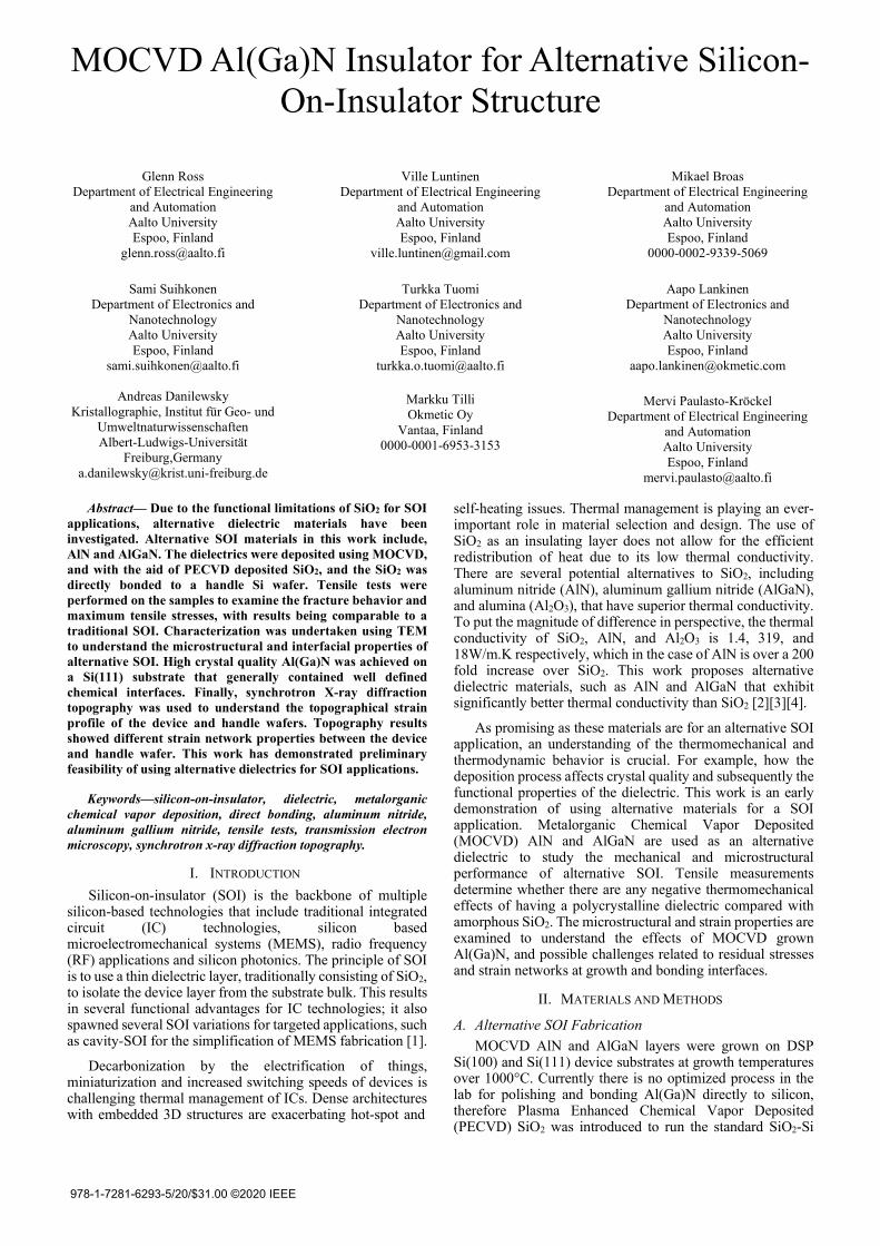
bonding process. A 500nm layer of PECVD SiO2 was deposited and annealed to remove excess hydrogen from the film to avoid void formation during bonding [1]. A Chemical Mechanical Polishing (CMP) and wafer cleaning process were undertaken to provide a suitable surface roughness for the direct bonding of the SiO2 surface. Direct bonding between the SiO2 polished surface and an SSP Si(100) handle wafer was carried out, followed by a post bonding anneal. Finally, the device wafer was thinned towards the Al(Ga)N growth interface. Fig. 1 illustrates the process flow and a list of the samples, substrate type, and thicknesses can be found in TABLE I.
Fig. 1. Shows the general process flow for the alternative SOI platform. (i) is the deposition of Al(Ga)N on Si (ii) is the deposition of PECVD SiO2, polishing and cleaning (iii) is the bonding process including post-bonding annealing and (iv) is final thinning of the device substrate revealing the final structure for characterization.
TABLE I. OVERVIEW OF THE SAMPLE NUMBER, SAMPLE STRUCTURE, SUBSTRATES AND THICKNESSES OF THE LAYERS
Sample Structure
Handle Si
Device Si SiO2 Al(Ga)N
- - [nm] [nm]
1 Si/SiO2/AlN/Si (100) (100) 130.5 ± 2.9 205.0 ± 2.9
2 Si/SiO2/AlN/Si (100) (111) 253.8 ± 0.3 206.8 ± 0.2
3 Si/SiO2/AlN/Si (100) (100) 206.4 ± 3.2 206.0 ± 3-2
4 Si/SiO2/AlN/Si (100) (111) 201.5 ± 0.3 126.6 ± 0.3
5 Si/SiO2/AlGaN/AlN/Si
(100) (111) 208.0 ± 0.1 202.2 ± 0.8
B. Tensile TestTensile tests were carried out using an MTS 858 Table
System using a Flex Test 40 digital control and an MTS SilentFlow HPU system (Fig. 2 (i)). The tensile test was based on a stud pull method. Sections of the bonded wafers were diced into 4.8 × 4.8𝑚𝑚𝑚𝑚2squares using a wafer dicer (Disco DAD3220). The diced sample pieces were mounted and glued between brass pull studs (Fig. 2 (ii)) using high-strength epoxy glue (Loctite® Power Epoxy Universal). Once the glue had hardened, the studs were mounted into the stud holders (Fig. 2 (iii)) and loaded into the tensile tester using hydraulic grippers.
Fig. 2. Is an overview the tensile test setup. Subfigure (i) is the MTS 858 table system, (ii) are the bonded sstamples glued to the studs and (iii) are the stud holders.
The tensile pull rate applied to the samples was 0.01mm/s and a sample population of 30 samples per wafer was chosen for statistical significance. All samples were measured until fracturing occurred. Optical fracture surface analysis was carried out to determine the fracture mode.
C. Microstrucutral CharaterisationSamples for the microstructural characterization were
prepared by first molding and cross-sectioning the bonded samples using a standard metallographic cross-sectioning procedure. The samples were pre-molded and cross-sectioned because the thinned device substrate was too thick to directly prepare a TEM lamella. TEM lamellas were prepared from the molded cross-sections using a dual-beam (FIB-SEM) JEOL JIB-4700F using an in-situ lift-out process. Transmission electron microscopy (TEM), scanning transmission electron microscopy (STEM), select area electron diffraction (SAED), and energy-dispersive X-ray spectroscopy (EDS) were conducted using the JEOL JEM-2800 operating at 200kV.
D. Synchrotron X-ray diffraction topographySynchrotron radiation X-ray diffraction topography (SR-
XRT) is a highly strain sensitive method for imaging (topographs) selected areas of single crystalline material. The measurements were recorded at the TOPO-TOMO beamline at ANKA (Angstromsquelle) in Karlsruhe [5]. The energy-dispersive diffraction diffracts several topographs from the irradiated volume onto an X-ray sensitive film. In energy dispersive mode, photons of energy E diffracts by lattice planes of interplanar spacing d when the Bragg condition is fulfilled (seen in equation 1), where h is Plank’s constant, c is the speed of light and 𝜃𝜃is the half angle.
ℎ𝑐𝑐/𝐸𝐸 = 2𝑑𝑑 sin(𝜃𝜃) (1)
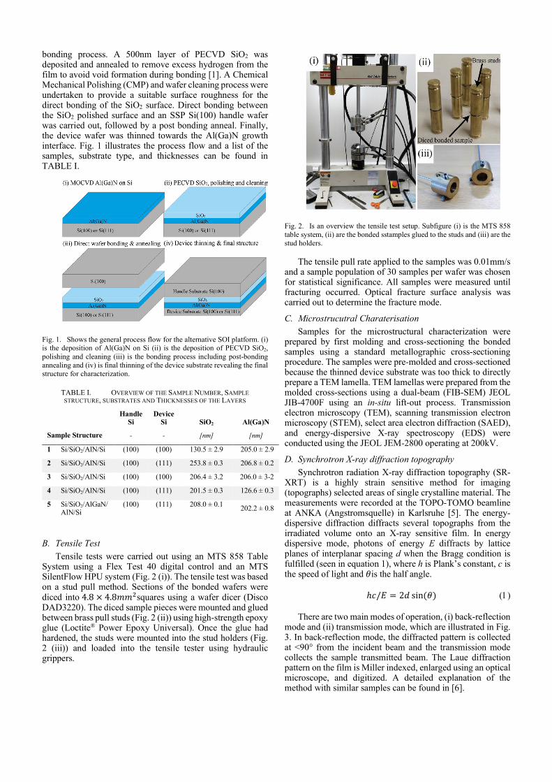
There are two main modes of operation, (i) back-reflection mode and (ii) transmission mode, which are illustrated in Fig. 3. In back-reflection mode, the diffracted pattern is collectedat <90° from the incident beam and the transmission modecollects the sample transmitted beam. The Laue diffractionpattern on the film is Miller indexed, enlarged using an opticalmicroscope, and digitized. A detailed explanation of themethod with similar samples can be found in [6].
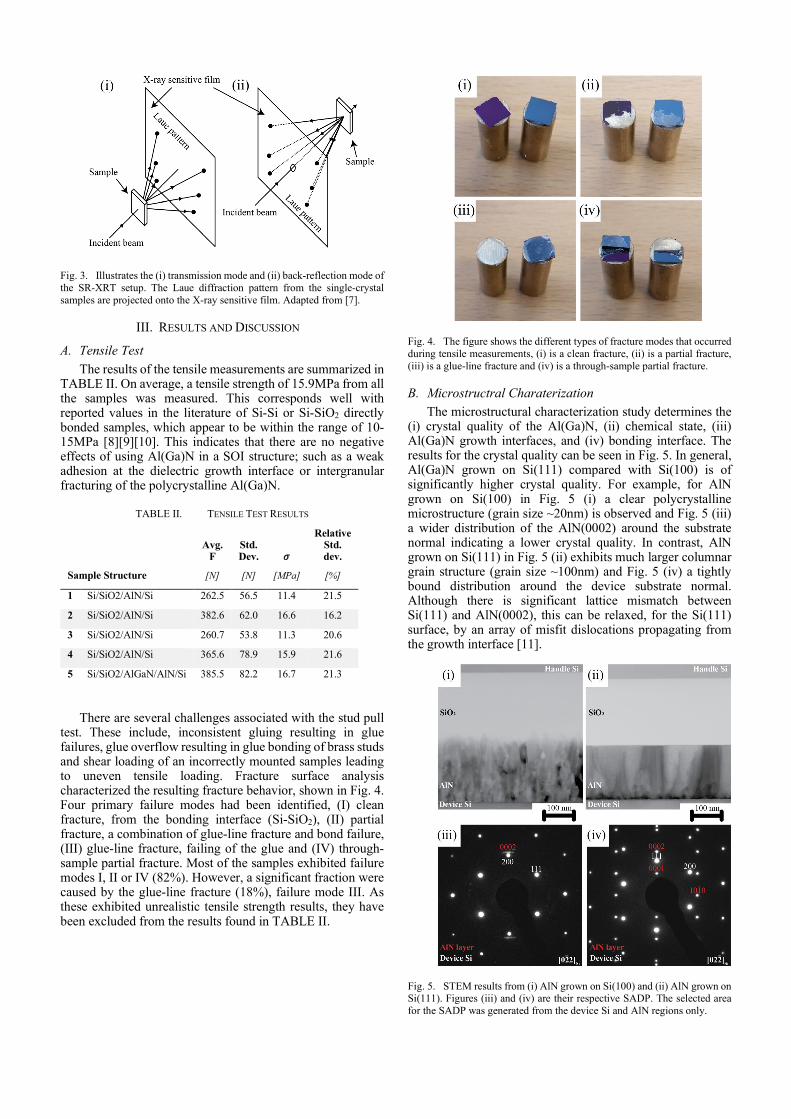
Fig. 3. Illustrates the (i) transmission mode and (ii) back-reflection mode of the SR-XRT setup. The Laue diffraction pattern from the single-crystal samples are projected onto the X-ray sensitive film. Adapted from [7].
III. RESULTS AND DISCUSSION
A. Tensile TestThe results of the tensile measurements are summarized in
TABLE II. On average, a tensile strength of 15.9MPa from all the samples was measured. This corresponds well with reported values in the literature of Si-Si or Si-SiO2 directly bonded samples, which appear to be within the range of 10-15MPa [8][9][10]. This indicates that there are no negative effects of using Al(Ga)N in a SOI structure; such as a weak adhesion at the dielectric growth interface or intergranular fracturing of the polycrystalline Al(Ga)N.
TABLE II. TENSILE TEST RESULTS
Sample Structure
Avg. F
Std.Dev. 𝜎𝜎
Relative Std. dev.
[N] [N] [MPa] [%]
1 Si/SiO2/AlN/Si 262.5 56.5 11.4 21.5
2 Si/SiO2/AlN/Si 382.6 62.0 16.6 16.2
3 Si/SiO2/AlN/Si 260.7 53.8 11.3 20.6
4 Si/SiO2/AlN/Si 365.6 78.9 15.9 21.6
5 Si/SiO2/AlGaN/AlN/Si 385.5 82.2 16.7 21.3
There are several challenges associated with the stud pull test. These include, inconsistent gluing resulting in glue failures, glue overflow resulting in glue bonding of brass studs and shear loading of an incorrectly mounted samples leading to uneven tensile loading. Fracture surface analysis characterized the resulting fracture behavior, shown in Fig. 4. Four primary failure modes had been identified, (I) clean fracture, from the bonding interface (Si-SiO2), (II) partial fracture, a combination of glue-line fracture and bond failure, (III) glue-line fracture, failing of the glue and (IV) through-sample partial fracture. Most of the samples exhibited failuremodes I, II or IV (82%). However, a significant fraction werecaused by the glue-line fracture (18%), failure mode III. Asthese exhibited unrealistic tensile strength results, they havebeen excluded from the results found in TABLE II.
Fig. 4. The figure shows the different types of fracture modes that occurred during tensile measurements, (i) is a clean fracture, (ii) is a partial fracture, (iii) is a glue-line fracture and (iv) is a through-sample partial fracture.
B. Microstructral CharaterizationThe microstructural characterization study determines the
(i) crystal quality of the Al(Ga)N, (ii) chemical state, (iii)Al(Ga)N growth interfaces, and (iv) bonding interface. Theresults for the crystal quality can be seen in Fig. 5. In general,Al(Ga)N grown on Si(111) compared with Si(100) is ofsignificantly higher crystal quality. For example, for AlNgrown on Si(100) in Fig. 5 (i) a clear polycrystallinemicrostructure (grain size ~20nm) is observed and Fig. 5 (iii)a wider distribution of the AlN(0002) around the substratenormal indicating a lower crystal quality. In contrast, AlNgrown on Si(111) in Fig. 5 (ii) exhibits much larger columnargrain structure (grain size ~100nm) and Fig. 5 (iv) a tightlybound distribution around the device substrate normal.Although there is significant lattice mismatch betweenSi(111) and AlN(0002), this can be relaxed, for the Si(111)surface, by an array of misfit dislocations propagating fromthe growth interface [11].
Fig. 5. STEM results from (i) AlN grown on Si(100) and (ii) AlN grown on Si(111). Figures (iii) and (iv) are their respective SADP. The selected area for the SADP was generated from the device Si and AlN regions only.
A summary of the sample crystal quality and Al(Ga)N/SiO2 interfacial roughness can be seen in TABLE III. The roughness of the Al(Ga)N layer is of interest. In asubsequent run of experiments, the aim would be to bondAl(Ga)N directly to Si handle. Ideally, from a processing andperformance point-of-view, it would be advantageous to bondthe dielectric layer directly with Si with a minimum of pre-processing steps (i.e. grinding, CMP, cleaning, etc.). A criticaldirect bonding parameter is the surface roughness, whichideally needs to be below 0.5nm [1] to achieve a good bond.Although slightly above this value (for Al(Ga)N grown onSi(111) wafers), only a minimal surface preparation could berequired to achieve a successful direct bond.
TABLE III. OVERVIEW OF THE AL(GA)N FILM QUALITY AND AL(GA)N/SIO2 INTERFACIAL ROUGHNESS (RMS)
Sample Structure Al(Ga)N (002) Rq1
[arcsec] [nm]
1 Si/SiO2/AlN/Si 49256 9.4
2 Si/SiO2/AlN/Si 7034 0.9
3 Si/SiO2/AlN/Si 56826 10.2
4 Si/SiO2/AlN/Si 10250 1.0
5 Si/SiO2/AlGaN/AlN/Si 8168 0.5
An example of the EDS chemical analysis of two samples can be seen in Fig. 6. Generally, all interfaces exhibit well-defined chemical interfaces with little to no interdiffusion of species. However, it has been observed at specific Al(Ga)N grain boundaries (indicated in the figure with a white arrow) the diffusion O into AlN, which can be seen along the SiO2/AlN interface in Fig. 6 (i). With the AlGaN sample there is an AlN layer followed by an AlGaN. The AlGaN epilayer requires a buffer layer to handle the lattice mismatch between Si and AlGaN layers. An EDS point analysis of the AlxGa1-x-
yNy showed a composition of x = 38.7 and y = 51.7.
Fig. 6. STEM-EDS results from (i) sample 2 and (ii) sample 5 with the AlGaN layer. Small white arrow indicates region of diffusion of O into AlN.
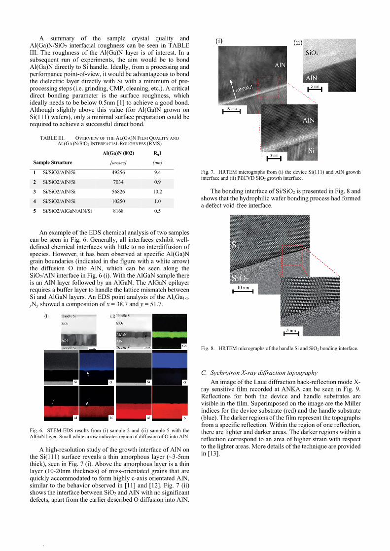
A high-resolution study of the growth interface of AlN on the Si(111) surface reveals a thin amorphous layer (~3-5nm thick), seen in Fig. 7 (i). Above the amorphous layer is a thin layer (10-20nm thickness) of miss-orientated grains that are quickly accommodated to form highly c-axis orientated AlN, similar to the behavior observed in [11] and [12]. Fig. 7 (ii) shows the interface between SiO2 and AlN with no significant defects, apart from the earlier described O diffusion into AlN.
Fig. 7. HRTEM micrographs from (i) the device Si(111) and AlN growth interface and (ii) PECVD SiO2 growth interface.
The bonding interface of Si/SiO2 is presented in Fig. 8 and shows that the hydrophilic wafer bonding process had formed a defect void-free interface.
Fig. 8. HRTEM micrographs of the handle Si and SiO2 bonding interface.
C. Sychrotron X-ray diffraction topographyAn image of the Laue diffraction back-reflection mode X-
ray sensitive film recorded at ANKA can be seen in Fig. 9. Reflections for both the device and handle substrates are visible in the film. Superimposed on the image are the Miller indices for the device substrate (red) and the handle substrate (blue). The darker regions of the film represent the topographs from a specific reflection. Within the region of one reflection, there are lighter and darker areas. The darker regions within a reflection correspond to an area of higher strain with respect to the lighter areas. More details of the technique are provided in [13].
.
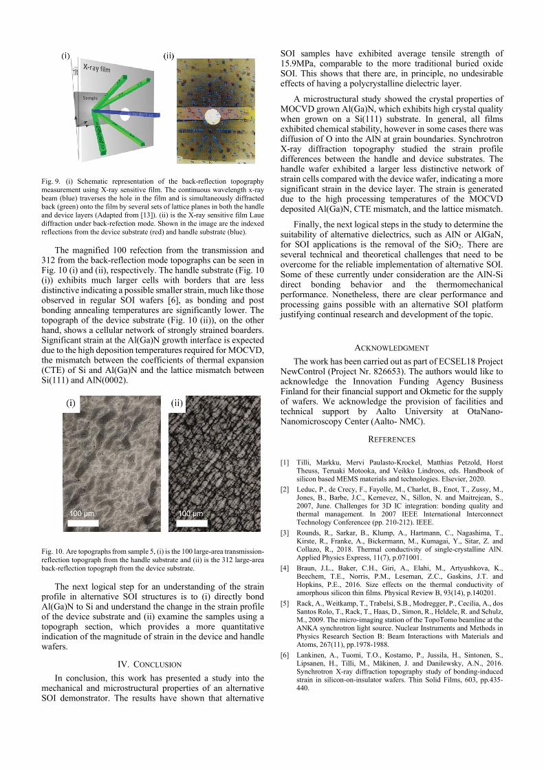
Fig. 9. (i) Schematic representation of the back-reflection topography measurement using X-ray sensitive film. The continuous wavelength x-ray beam (blue) traverses the hole in the film and is simultaneously diffracted back (green) onto the film by several sets of lattice planes in both the handle and device layers (Adapted from [13]). (ii) is the X-ray sensitive film Laue diffraction under back-refection mode. Shown in the image are the indexed reflections from the device substrate (red) and handle substrate (blue).
The magnified 100 refection from the transmission and 312 from the back-reflection mode topographs can be seen in Fig. 10 (i) and (ii), respectively. The handle substrate (Fig. 10 (i)) exhibits much larger cells with borders that are less distinctive indicating a possible smaller strain, much like those observed in regular SOI wafers [6], as bonding and post bonding annealing temperatures are significantly lower. The topograph of the device substrate (Fig. 10 (ii)), on the other hand, shows a cellular network of strongly strained boarders. Significant strain at the Al(Ga)N growth interface is expected due to the high deposition temperatures required for MOCVD, the mismatch between the coefficients of thermal expansion (CTE) of Si and Al(Ga)N and the lattice mismatch between Si(111) and AlN(0002).
Fig. 10. Are topographs from sample 5, (i) is the 100 large-area transmission-reflection topograph from the handle substrate and (ii) is the 312 large-area back-reflection topograph from the device substrate.
The next logical step for an understanding of the strain profile in alternative SOI structures is to (i) directly bond Al(Ga)N to Si and understand the change in the strain profile of the device substrate and (ii) examine the samples using a topograph section, which provides a more quantitative indication of the magnitude of strain in the device and handle wafers.
IV. CONCLUSION
In conclusion, this work has presented a study into the mechanical and microstructural properties of an alternative SOI demonstrator. The results have shown that alternative
SOI samples have exhibited average tensile strength of 15.9MPa, comparable to the more traditional buried oxide SOI. This shows that there are, in principle, no undesirable effects of having a polycrystalline dielectric layer.
A microstructural study showed the crystal properties of MOCVD grown Al(Ga)N, which exhibits high crystal quality when grown on a Si(111) substrate. In general, all films exhibited chemical stability, however in some cases there was diffusion of O into the AlN at grain boundaries. Synchrotron X-ray diffraction topography studied the strain profiledifferences between the handle and device substrates. Thehandle wafer exhibited a larger less distinctive network ofstrain cells compared with the device wafer, indicating a moresignificant strain in the device layer. The strain is generateddue to the high processing temperatures of the MOCVDdeposited Al(Ga)N, CTE mismatch, and the lattice mismatch.
Finally, the next logical steps in the study to determine the suitability of alternative dielectrics, such as AlN or AlGaN, for SOI applications is the removal of the SiO2. There are several technical and theoretical challenges that need to be overcome for the reliable implementation of alternative SOI. Some of these currently under consideration are the AlN-Si direct bonding behavior and the thermomechanical performance. Nonetheless, there are clear performance and processing gains possible with an alternative SOI platform justifying continual research and development of the topic.
ACKNOWLEDGMENT The work has been carried out as part of ECSEL18 Project
NewControl (Project Nr. 826653). The authors would like to acknowledge the Innovation Funding Agency Business Finland for their financial support and Okmetic for the supply of wafers. We acknowledge the provision of facilities and technical support by Aalto University at OtaNano-Nanomicroscopy Center (Aalto- NMC).
REFERENCES
[1] Tilli, Markku, Mervi Paulasto-Krockel, Matthias Petzold, HorstTheuss, Teruaki Motooka, and Veikko Lindroos, eds. Handbook ofsilicon based MEMS materials and technologies. Elsevier, 2020.
[2] Leduc, P., de Crecy, F., Fayolle, M., Charlet, B., Enot, T., Zussy, M.,Jones, B., Barbe, J.C., Kernevez, N., Sillon, N. and Maitrejean, S.,2007, June. Challenges for 3D IC integration: bonding quality andthermal management. In 2007 IEEE International InterconnectTechnology Conferencee (pp. 210-212). IEEE.
[3] Rounds, R., Sarkar, B., Klump, A., Hartmann, C., Nagashima, T.,Kirste, R., Franke, A., Bickermann, M., Kumagai, Y., Sitar, Z. andCollazo, R., 2018. Thermal conductivity of single-crystalline AlN.Applied Physics Express, 11(7), p.071001.
[4] Braun, J.L., Baker, C.H., Giri, A., Elahi, M., Artyushkova, K.,Beechem, T.E., Norris, P.M., Leseman, Z.C., Gaskins, J.T. andHopkins, P.E., 2016. Size effects on the thermal conductivity ofamorphous silicon thin films. Physical Review B, 93(14), p.140201.
[5] Rack, A., Weitkamp, T., Trabelsi, S.B., Modregger, P., Cecilia, A., dos Santos Rolo, T., Rack, T., Haas, D., Simon, R., Heldele, R. and Schulz, M., 2009. The micro-imaging station of the TopoTomo beamline at the ANKA synchrotron light source. Nuclear Instruments and Methods inPhysics Research Section B: Beam Interactions with Materials andAtoms, 267(11), pp.1978-1988.
[6] Lankinen, A., Tuomi, T.O., Kostamo, P., Jussila, H., Sintonen, S.,Lipsanen, H., Tilli, M., Mäkinen, J. and Danilewsky, A.N., 2016.Synchrotron X-ray diffraction topography study of bonding-induced strain in silicon-on-insulator wafers. Thin Solid Films, 603, pp.435-440.

[7] “PhysicsOpenLab - Laue Diffraction,” Jan. 18, 2018. Accessed on: Jul.10, 2020. [Online]. Available: http://www.http://physicsopenlab.org/2018/01/18/laue-diffraction/
[8] Takagi, H., Maeda, R., Chung, T.R., Hosoda, N. and Suga, T., 1998.Effect of surface roughness on room-temperature wafer bonding by Ar beam surface activation. Japanese journal of applied physics, 37(7R),p.4197.
[9] Takagi, H., Maeda, R., Chung, T.R. and Suga, T., 1998. Low-temperature direct bonding of silicon and silicon dioxide by the surface activation method. Sensors and Actuators A: Physical, 70(1-2), pp.164-170.
[10] Kräuter, G., Schumacher, A. and Gösele, U., 1998. Low temperaturesilicon direct bonding for application in micromechanics: bonding
energies for different combinations of oxides. Sensors and Actuators A: Physical, 70(3), pp.271-275.
[11] Liu, R., Ponce, F.A., Dadgar, A. and Krost, A., 2003. Atomicarrangement at the AlN/Si (111) interface. Applied Physics Letters,83(5), pp.860-862.
[12] Lahrèche, H., Vennéguès, P., Tottereau, O., Laügt, M., Lorenzini, P.,Leroux, M., Beaumont, B. and Gibart, P., 2000. Optimisation of AlNand GaN growth by metalorganic vapour-phase epitaxy (MOVPE) onSi (1 1 1). Journal of crystal growth, 217(1-2), pp.13-25.
[13] S. Sintonen, M. Rudziński, S. Suihkonen, H. Jussila, M. Knetzger, E.Meissner, A. Danilewsky, T. O. Tuomi, H. Lipsanen, J. Appl. Phys.2014, 116, 83504.