Embed Size (px)
Citation preview
RP-M2455AP
Datasheet V1.1
(No. BRP0101)
BRP0101 RP-M2455AP Datasheet
V1.1 Page:2/14
www.radiopulse.co.kr
REVISION HISTORY
Version Date Description
V1.0 2013.10.16 ▪ First Version Release.
V1.1 2014.09.17
▪ Attention is added in Sec 3.1.
- Do not use external connection about Pin9 (P1_7)
and Pin18 (P3_4).
- Pin9 (P1_7) and Pin18 (P3_4) are NC for external
Board.
BRP0101 RP-M2455AP Datasheet
V1.1 Page:3/14
www.radiopulse.co.kr
CONTENTS
1. FEATURES .............................................................................................................................................. 4
1.1. DESCRIPTION ........................................................................................................................................................ 4
1.2. DRAWING .............................................................................................................................................................. 6
1.2.1. Outline Top View ............................................................................................................................................ 6
1.2.2. PCB drawing Top View ................................................................................................................................ 7
1.2.3. PCB (top view) .............................................................................................................................................. 8
1.2.4. Module Block Diagram ............................................................................................................................... 8
2. ELECTRICAL SPECIFICATIONS ........................................................................................................... 9
2.1. ABSOLUTE MAXIMUM RATINGS ........................................................................................................................ 9
2.2. DC CHARACTERISTICS ......................................................................................................................................... 9
2.3. ELECTRICAL SPECIFICATIONS .............................................................................................................................. 9
2.4. RF CHARACTERISTICS(+25℃) ....................................................................................................................... 10
2.5. ENVIRONMENT CONDITION ............................................................................................................................ 10
3. SCHEMATIC FOR APPLICATION ...................................................................................................... 11
3.1. PIN DESCRIPTION ............................................................................................................................................. 11
3.2. MODULE CIRCUIT ............................................................................................................................................. 12
3.3. PARTS LIST ......................................................................................................................................................... 13
BRP0101 RP-M2455AP Datasheet
V1.1 Page:4/14
www.radiopulse.co.kr
1. FEATURES
This specification is applied to IEEE802.15.4 & RF4CE Module. This module is embedded with Amplifier, 16MHz X-TAL and Single chip.
1.1. Description
RF Transceiver
■ Single-chip 2.4 ~ 2.4835GHz RF Transceiver
■ Low Power Consumption
■ Low Operating Voltage of 1.5V
■ High Sensitivity of -98dBm at [email protected]
■ No External T/R Switch or Filter Needed
■ On-chip VCO, LNA, and PA
■ Programmable Output Power up to [email protected]
■ Direct Sequence Spread Spectrum
■ O-QPSK Modulation
■ Scalable Data Rate Including 250Kbps Specified in IEEE 802.15.4: 250Kbps ~
1Mbps
■ RSSI Measurement
■ Compliant to IEEE 802.15.4
Hardwired MAC
■ Two 256-byte Circular FIFOs
■ FIFO Management
■ AES-128 Engine
■ CRC-16 computation and check
8051-Compatible MCU
■ Max. 12x Performance of standard 8051
■ 96KB embedded flash memory
■ 8KB data memory
■ 128-byte CPU Dedicated memory
■ 1KB Boot ROM
■ Dual DPTR support
■ I2S/PCM interface with two 128-byte FIFOs
■ µ-law/a-law/ADPCM voice Codec
■ Two high-speed UARTs with two 16-byte FIFOs(up to 1Mbps)
■ 4 timers/2 PWMs
■ Watchdog timer
BRP0101 RP-M2455AP Datasheet
V1.1 Page:5/14
www.radiopulse.co.kr
■ Sleep timer
■ Quadrature Signal Decoder
■ 22 General Purpose I/Os
■ Internal RC Oscillator for sleep timer
■ On-chip Power-on-Reset
■ 4-Channel 8-bit ADC)
■ SPI Master/Slave Interface
■ ISP (In System Programming)
■ Temperature Sensor
Clock Inputs
■ 16MHz crystal for system clock
Power
■ When using Internal Regulator of MG2455
1.5V (Core)/1.9 ~ 3.3V (I/O) operation
■ When NOT using Internal Regulator of MG2455
1.5V (Core)/1.5V (I/O) operation
■ Power management scheme with deep sleep mode Support
■ Two On-chip Voltage Regulator for Analog part and Digital part separately
■ Power supply range for internal regulator(1.9V(Min) ~ 3.6V(Max))
■ Battery Monitoring Support
Front-End Module FEATURES
■ Transmitter output power <+18dBm
■ Receiver path NF<2.5dB
■ Internal switching and control circuits
■ Configurable transmit/receive paths
■ Internal RF match and bias circuits
■ Single DC supply= 3.3V
■ All RF parts are internally DC blocked
Package
■ 38-pin, 16X22 mm SMT package
BRP0101 RP-M2455AP Datasheet
V1.1 Page:6/14
www.radiopulse.co.kr
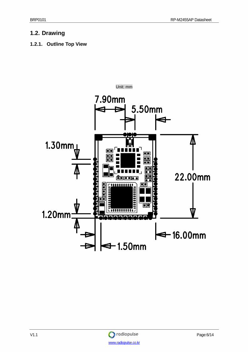
1.2. Drawing
1.2.1. Outline Top View
Unit: mm
BRP0101 RP-M2455AP Datasheet
V1.1 Page:7/14
www.radiopulse.co.kr
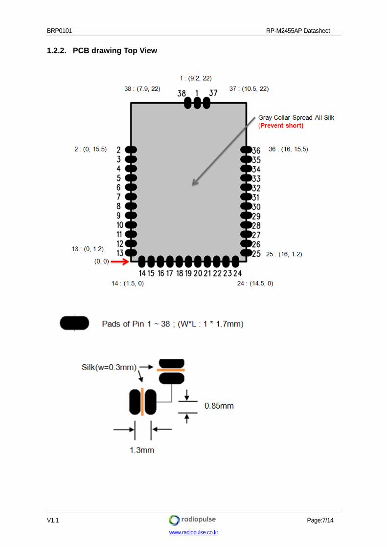
1.2.2. PCB drawing Top View
BRP0101 RP-M2455AP Datasheet
V1.1 Page:8/14
www.radiopulse.co.kr
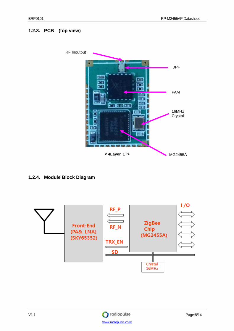
1.2.3. PCB (top view)
< 4Layer, 1T>
1.2.4. Module Block Diagram
PAM
MG2455A
16MHz Crystal
RF Inoutput
BPF
BRP0101 RP-M2455AP Datasheet
V1.1 Page:9/14
www.radiopulse.co.kr
2. ELECTRICAL SPECIFICATIONS
2.1. Absolute Maximum Ratings
2.2. DC Characteristics
Symbol Parameter Min Typ. Max Unit
VDD Chip core supply voltage
(AVDD_1.5V,DVDD_1.5V) 1.35 1.5 1.65 V
VDDIO I/O supply voltage(3V_IN) 1.35(*) 3.0 3.3 V
VIH High level input voltage 0.7X VDDIO VDDIO V
VIL Low level input voltage 0 0.3X
VDDIO V
VOH High level output voltage VDDIO -0.5 VDDIO V
VOL Low level output voltage 0 0.4 V
TA Air temperature -20 70 ℃
(*) : MSV= output voltage(regulator drop voltage), 3VIN=2.7~3.3V is Recommended.
Note) All voltage values are based on ground. All input and output voltage levels are TTL-compatible.
2.3. Electrical Specifications (Condition: EVM Board , at 25℃, VCC _IN=3.3V, VDD(AVDD,DVDD=1.5V)
Item Spec Remark
Supply input voltage +3.3Vdc
Normal Mode TX: 158mA RX: 42mA
TX Output Level: 17.8dBm
Sleep Current PM1 (BOD enable)
64A Max : 149uA
Symbol Parameter Rating Unit
VDD Chip core supply voltage -0.3 to 1.65 V
VDDIO I/O supply voltage(3V_IN) -0.3 to 3.3 V
RFIN Input RF level 10 dBm
TSTG Storage Temperature -30 to 80 ℃
ESD
HBM(JESD22-A114-F) 2000 V
MM(JESD22-A115-A) 150 V
CDM(JESD22-C101-E) 500 V
BRP0101 RP-M2455AP Datasheet
V1.1 Page:10/14
www.radiopulse.co.kr
2.4. RF Characteristics(+25℃)
Item Spec Remark
Frequency Range 2405~2483.5MHz
Frequency Tolerance <±20ppm
Occupied B.W <2.2MHz
Output Power (Normal) MAX18dBm (+0/-2dB)
VSWR <2.0 : 1
Flatness <2dB
Spurious Emissions 1GHz Under 1GHz ~ 2.4GHz 2.4GHz ~ 3GHz
3GHz ~ 12GHz
<-50dBm <-50dBm <-33dBm <-50dBm
2nd Harmonic <-50dBm
3rd Harmonic <-50dBm
PSD ±3.5MHz >30dBc 20dBc over
Secondary Radiated Emission
<-70dBm Limit of secondary radiated emissions. -54dBm under
Rx Sensitivity <-98dBm 22-byte, 1%
2.5. Environment Condition
Item Spec. Remarks
Storage Temp. -30 ~ +80 ℃
Operating Temp. -20 ~ +70 ℃

BRP0101 RP-M2455AP Datasheet
V1.1 Page:11/14
www.radiopulse.co.kr
3. SCHEMATIC for APPLICATION
3.1. Pin Description
Terminal NAME Inter face I/O Description
1 RF_INOUT
2 ACH0 Analog I/O Sensor ADC input
3 ACH1 Analog I/O Sensor ADC input
4 ACH2 Analog I/O Sensor ADC input
5 ACH3 Analog I/O Sensor ADC input
6 GND Ground - Ground
7 ISP Digital I ISP
8 RESETB Digital I Reset (Active Low)
9 P1[7] Digital O Port P1.7GPO/P0AND/TRSW
10 P1[6] Digital B Port P1.6/TRSWB
11 P1[4] Digital B Port P1.4 /QUADZB/Sleep Timer OSC Buffer Input.
12 P1[3] Digital B Port P1.3/QUADZA/Sleep Timer OSC Buffer Output/RTCLKOUT
13 P1[1] Digital B Port P1.1/TXD1
14 P1[0] Digital B Port P1.0/RXD1
15 P3[7] Digital B Port P3.7/12mA Drive capability /PWM3/CTS1/SPICSN(slave only)
16 P3[6] Digital B Port P3.6/12 mA Drive capability /PWM2/RTS1/SPICLK
17 P3[5] Digital B Port P3.5/T1/CTS0/QUADYB/SPIDO
18 P3[4] Digital B Port P3.4/T0/RTS0/QUADYA/SPIDI
19 P3[3] Digital B Port P3.3/INT1(active low)
20 P3[2] Digital B Port P3.2/INT0(active low)
21 P3[1] Digital B Port P3.1/TXD0/QUADXB
22 3.3V_IN Power I 3.3V Power supply
23 GND Ground - Ground
24 GND Ground - Ground
25 P3[0] Digital B Port P3.0/RXD0/QUADXA
26 P0[7] Digital B Port P0.7/I2STX_MCLK
27 P0[6] Digital B Port P0.6/I2STX_BCLK
28 P0[5] Digital B Port P0.5/I2STX_LRCK
29 P0[4] Digital B Port P0.4/I2STX_DO
30 P0[3] Digital B Port P0.3/I2SRX_MCLK
31 P0[2] Digital B Port P0.2/I2SRX_BCLK
32 P0[1] Digital B Port P0.1/I2SRX_LRCK
33 P0[0] Digital B Port P0.0/I2SRX_DI
34 GND Ground - Ground
35 GND Ground - Ground
36 GND Ground - Ground
37 GND Ground - Ground
38 GND Ground - Ground
BRP0101 RP-M2455AP Datasheet
V1.1 Page:12/14
www.radiopulse.co.kr
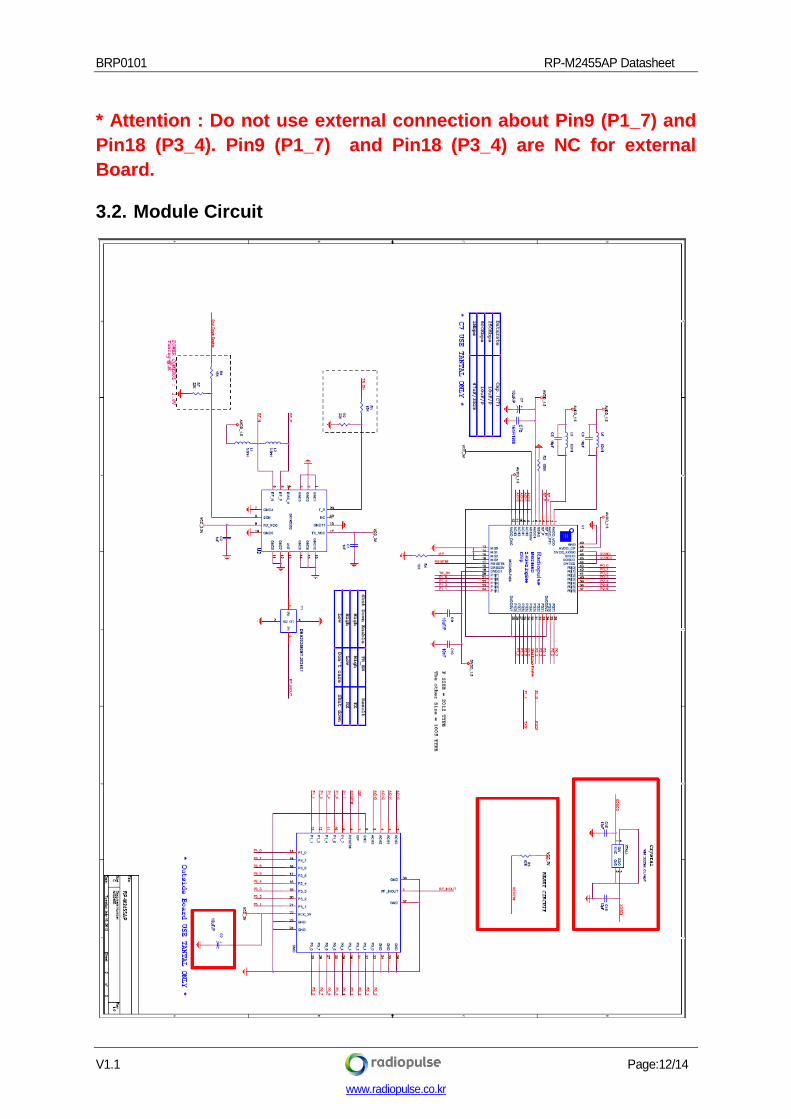
* Attention : Do not use external connection about Pin9 (P1_7) and
Pin18 (P3_4). Pin9 (P1_7) and Pin18 (P3_4) are NC for external
Board.
3.2. Module Circuit
BRP0101 RP-M2455AP Datasheet
V1.1 Page:13/14
www.radiopulse.co.kr
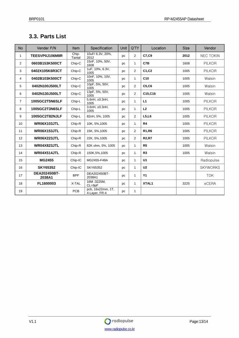
3.3. Parts List
No Vender P/N Item Specification Unit Q'TY Location Size Vendor
1 TEESVP0J106M8R Chip-Tantal
10uF/ 6.3V, 20%, 2012
pc 2 C7,C9 2012 NEC TOKIN
2 0603B153K500CT Chip-C 15nF, 10%, 50V, 1608
pc 1 C7B 1608 PILKOR
3 0402X105K6R3CT Chip-C 1uF, 10%, 6.3V, 1005
pc 2 C1,C2 1005 PILKOR
4 0402B103K500CT Chip-C 10nF, 10%, 10V, 1005
pc 1 C10 1005 Walsin
5 0402N100J500LT Chip-C 10pF, 5%, 50V, 1005
pc 2 C5,C6 1005 Walsin
6 0402N130J500LT Chip-C 13pF, 5%, 50V, 1005
pc 2 C15,C16 1005 Walsin
7 1005GC2T5N6SLF Chip-L 5.6nH, ±0.3nH, 1005
pc 1 L1 1005 PILKOR
8 1005GC2T3N6SLF Chip-L 3.6nH, ±0.3nH, 1005
pc 1 L2 1005 PILKOR
9 1005GC2T82NJLF Chip-L 82nH, 5%, 1005 pc 2 L5,L6 1005 PILKOR
10 WR06X103JTL Chip-R 10K, 5%,1005 pc 1 R4 1005 PILKOR
11 WR06X153JTL Chip-R 15K, 5%,1005 pc 2 R1,R6 1005 PILKOR
12 WR06X223JTL Chip-R 22K, 5%,1005 pc 2 R2,R7 1005 PILKOR
13 WR04X823JTL Chip-R 82K ohm, 5%, 1005 pc 1 R5 1005 Walsin
14 WR04X514JTL Chip-R 150K,5%,1005 pc 1 R3 1005 Walsin
15 MG2455 Chip-IC MG2455-F48A pc 1 U1 Radiopulse
16 SKY65352 Chip-IC SKY65352 pc 1 U2 SKYWORKS
17 DEA202450BT-
2038A1 BPF
DEA202450BT-2038A1
pc 1 Y1
TDK
18 FL1600003 X-TAL 16M :3225M, CL=9pF
pc 1 XTAL1 3225 eCERA
19 PCB pcb, 16x22mm, 1T, 4-Layer, FR-4
pc 1
BRP0101 RP-M2455AP Datasheet
V1.1 Page:14/14
www.radiopulse.co.kr
RadioPulse Inc
3rd Fl., Hans B/D II, 111-6 Seongnae-Dong,
Gangdong-Gu, Seoul, Korea, 134-883, Korea
URL: www.radiopulse.co.kr
Tel: +82-2-478-2963~5
Fax: +82-2-478-2967
About RadioPulse Inc.
RadioPulse is a Being Wireless solution provider offering wireless communication & network
technologies and developing next generation wireless networking technologies.
The new wireless networking solutions envisioned by RadioPulse will enable user to enjoy wireless
technologies with easy interface.
Founded in April of 2003, the company maintains it headquarters and R&D center in Seoul, Korea.
Copyright (c) 2014 RadioPulse. All rights reserved.


![[MG2460] Datasheet - IXYS Corporation: IXYS Powerixapps.ixys.com/DataSheet/ADS0601-[MG2460]_Datash… · · 2015-08-135.1. ABSOLUTE MAXIMUM RATINGS ... ADS0601 MG2460 Datasheet](https://img.pdfslide.net/doc/110x75/5aef32107f8b9aa9168c3b16/mg2460-datasheet-ixys-corporation-ixys-mg2460datash2015-08-1351-absolute.jpg)