Embed Size (px)
Citation preview

{Gnu-nut
- ' cu A’r‘ n-~4|v~'lll| u .u .15- : l:9vl-vv!"k'v'.!‘ "":\',"rt~-‘l‘.'-'
"HE“
IIIIIIIIIIIIIIIIIIIIIIIIIIIIIIIIIIIIIIIIII‘II'III31293 00895 2883
This is to certify that the
thesis entitled
SSPICE: A SYMBOLIC ANALYZER 0F
LINEAR ACTIVE CIRCUITS
presented by
Anupam Srivastava
has been accepted towards fulfillment
of the requirements for
Master's degree in Electrical
Engineering
%M/
Major professor
Date £9 5 //7/&
0/
0-7639 MSU is an Affirmative Action/Equal Opportunity Institution

_.._...
r *1
LIBRARY
Michigan State
University J
A
h
PLACE IN RETURN BOX to remove this checkout from your record.
TO AVOID FINES return on or before date due.
DATE DUE DATE DUE DATE DUE
MSU lc An Affirmative Action/Equal Opportunity Inditution
cMma-c:
SSPICE: A SYMBOLIC ANALYZER OF LINEARACI'IVE CIRCUITS
By
Anupam Srivastava
A THESIS
Submitted to
Michigan State University
in partial fulfillment of the requirements
for the degree of
MASTER OF SCIENCE
Department of Electrical Engineering
1990
ABSTRACT
SSPICE: A SYMBOLIC ANALYZER OF LINEAR ACTIVE CIRCUITS
Anupam Srivastava
Understanding the small signal behaviom' of a circuit is a key element of circuit
design. A variety of circuit simulators are available in the market that can simulate
the frequency response of a circuit, given the value of the circuit parameters. How-
ever, deeper insight into circuit behaviom' can be gained if circuit parameters are
treated as symbols instead of as numbers; The final result is then symbolic instead
of numeric and explicitly embodies the role of each circuit parameter in the behav-
iom' of the circuit. Symbolic computation involves manipulating strings of symbols
and often generates large, unwieldy results. Thus, some measure of numerical analysis
must accompany symbolic analysis so that only the dominant symbolic terms are
generated. This process, termed symbolic approximation, helps keep symbolic results
tractable and preserves most of their semantics. Sspice is a software tool, developed
at MSU, that automates the symbolic analysis of linear active circuits.

Dedicated To Poochie, The Triple A Fraternity,and my main men - Ponniah, VI, and Inder
iii

ACKNOWLEDGEMENTS
I am deeply grateful to Shoba Krishnan and Sriman Ramabhadr'an for the selfless manner
in which they helped me complete this thesis on time.
I am personally indebted to Dr. Wierzba for his constant support and guidance.
iv

TABLE OF CONTENTS
LIST OF TABLES...........................................................................................................vii
LIST OF FIGURES........................................................................................................viii
I. The symbolic analysis paradigm and the Sspice solution................................................. 1
1.1 Introduction to symbolic analysis.............................................................................. l
1.2 The Sspice approach..................................................................................................2
II. Theoretical Basis of Sspice..............................................................................................5
2.1 Introducdon to nodal analysis....................................................................................5
2.2 Passive network analysis............................................................................................6
2.3 Introduction to nullators and norators........................................................................7
2.4 Active network analysis.............................................................................................8
2.5 Active filter design using symbolic transfer functions............................................ 11
2.5.1 Low pass filter function................................................................................ 11
2.5.2 High pass filter function............................................................................... 12
2.5.3 Band pass filter function............................................................................... 12
2.5.4 Notch filter function...................................................................................... 13
2.5.5 All pass filter function.................................................................................. 13
2.6 Estimating deviance in filter parameters.................................................................. 14
III. Numerical Evaluation and Symbolic Approximation............................................... 16
3.1 Drawbacks of symbolic computation.................................................................... 16
3.2 Mitigating problems through symbolic approximation......................................... 16
IV. Operational Specifics and Salient Features.................................................................. 19
4.1 Behavioral description of Sspice modules............................................................. 19
4.2 Overall operation.................................................................................................... 19
4.3 Error detection and recovery..................................................................................20
4.4 User friendly features.............................................................................................21
4.5 Operational description of Sspice modules............................................................21
4.5.1 Module 1: Forming nodal equations.........................................................21
4.5.2 Module II: Solving nodal equations.........................................................22
4.5.2.1 Example.................................................................................................25
4.5.3 Module III: Filter function identification.................................................26
4.5.4 Module IV: Estimating deviance due to non ideal effects.......................26
4.6 Conclusion............................................................................................................27
V. Future Directions..........................................................................................................28 .
APPENDIX A. Input Format And Modelling of Sspice Elements............................30
APPENDIX B. Illustrative Example: State Variable Active Filter..................................44
APPENDIX C. Illustrative Example: CMOS Op-Amp...................................................49
APPENDIX D. Interactive structure of Sspice................................................................58
D 1.1 Key to interactive prompts...............................................................................60
BIBLIOGRAPHY..............................................................................................................61
vi
LIST OF TABLES
4.1. Execution trace of determinant algorithm.............................................................25
BI. Sspice Input file SVAF.CIR..................................................................................45
132. Sspice Output file SVAFFUN ...............................................46
B3. Sspice Output file SVAFERR .............................................................................48
C1. PSpice/Sspice Input File...........................................................................................50
C2. PSpice Output File Bias Point Values..................................................................50
C3. Sspice Output file CMOS.DET..............................................................................52
C4. Sspice Approximated Output file CMOS.DET.....................................................54
vi 1
LIST OF FIGURES
1. Resismr model and input specification..................................................................30
2. Capacitor model and input specification................................................................3O
3. Independent cm'rent some model (normalized to one).......................................30
4. Nullator Norator pair................................................................................................31
5. DC cmrent source model (open circuit).................... .............................................3 1
6. AC voltage source model (normalized to one).....................................................31
7. DC Voltage source model (short circuit)...............................................................32
8. Source transformed AC current source model......................................................32
9. Source transformed AC current source model......................................................32
10. Inductor model........................................................................................................33
11. Voltage Controlled Current Source model (Gain = GM)..................................33
12. Coupling Capacitor Model (short circuit)............................................................33
13. Voltage controlled voltage source model (Gain = A)........................................34
14. Current controlled current sorn'ce (Gain = B)-- - -- - 34
15. Current controlled voltage source model (Gain = RM).....................................35
16. Voltage controlled voltage somce (Gain = UK).................................................35
17. Lowest level diode model (short circuit).............................................................36
18. Low frequency diode model ................................................................................36
19. High frequency diode model.................................................................................36
20. Simplest hybrid pi model of a BIT (Gain = GM)............................................37
21. Simplest hybrid pi model of a BIT (Gain = B)- _- ............................37
22. Low frequency hybrid pi model of a BJT ........................................................38
23. High frequency hybrid pi model of a BIT..........................................................38
24. Lowest level JFETmodel . - 39
25. Low frequency JFET model...................................................................................39
26. High frequency JFET model..................................................................................4O
27. Lowest level MOSFET model................................................................................40
28. Low frequency MOSFET model............................................................................41
29. High frequency MOSFET model...........................................................................41
30. Ideal operational amplifier model..........................................................................42
31. Non-ideal op amp model........................................................................................42
viii
32. Operational transconductanee amplifier model .......................................................43
33. Transformer model with N:l turns ratio.......................................................................43
B1. State Variable Active Filter ...................... - _ ................ --44
C1. CMOS op-arnp.-- -- --....49
C2. Open loop gain circuit - ............49
C3. Open loop magnitude comparison ofPSpice andSspice.-- ........ . 55
C4. Open loop phase response comparison ofPSpice and Sspice -- 56
D1. Interactive structme of Module I....... - ...... - -- 58
D2. Interactive structtn'e ofModule II - -- - -- - .... 59
i-x

CI-IAPTERI
The symbolic analysis paradigm and the Sspice solution
1.1 INTRODUCTION TO SYMBOLIC ANALYSIS
Sspice is an acronym for SymbolicSPICE. It is a software tool for small signal,
symbolic analysis of linear active circuits. Symbolic analysis is superior to behav-
ioral simulation of circuits from a circuit designer’s perspective since it records the
identity of each circuit parameter in the final result. A symbolic result is dependent
only on the circuit structure and is independent of any numerical instance of circuit
parameters. All instances of a circuit that can be derived by varying its parameter
values are encapsulated in one symbolic result. Behavioral simulation, on the other
hand, analyzes one instance of a circuit. Moreover, it combines the contributions of
various circuit parameters into a numeric result. The number itself is anonymous,
and offers no insight into its pedigree. Behavioral simulation is simply a numerical
evaluation of the symbolic result for a given set of parameter values. Its use is
more appropriate during the verification and testing stage of circuit design. The de—
sign Stage requires a deeper understanding of circuit semantics and symbolic analy-
sis is means to. this end.
Circuit analysis involves building a set of equations from a Circuit’s description and
then solving for the unknown currents and voltages in the circuit. It is possible to
build circuit equations by mere inspection and without any prior knowledge of
circuit theory. Sspice models each circuit element by a well defined set of primitive
elements - resistors, capacitors, independent current sources, nullators, and norators.
It produces a matrix formulation of circuit equations and solves for the unknowns
by computing the determinant of the corresponding matrices. In fact, Sspice can
analyze any process that reduces to a set of linear, independent, simultaneous
equations. Sspice was developed primarily for active filter design. It detects any
second order filter functions in the circuit, and solves for the ideal values of filter

2
parameters. The non-ideal efi'ects of operational amplifiers in a circuit can shift the
filter parameters from their ideal values. Provided that these shifts are small in
magnitude, it is possible to compute a symbolic estimate of errors in terms of
circuit parameters. The circuit designer can then minimize these errors by assigning
appropriate values to circuit parameters. Some successful results have already been
found and published using this strategy[l].
A frequent criticism of symbolic analysis is that it generates large amounts of data
even for moderately sized problems. One approach is to choose circuits that have
simple design equations and analyze them fmther. However, most of the time the
designer does not know the final answer but just needs a handle on the circuit pa-
rameters that dominate the behavior of the circuit. Sspice can generate an approxi-
mated symbolic result given the values of the circuit parameters. This feature is
invaluable in transistor design where the circuits are complicated and the exact
symbolic result is intractable. It is clear that the approximated result is dependent
on parameter values but this dependence is minor and is outweighed by the gain in
insight.
1.2 THE SSPICE APPROACH
Symbolic computation involves manipulations on strings and unfortunately, most of
them involve concatenation. The symbolic result of a computation can quickly in-
crease in size and thus, emciency is a major issue in automatic symbolic analysis.
Sspice is implemented in ‘C’ for this reason as well as for its rich variety of string
handling functions. Sspice is available on SUN, VAX and HP platforms. A micro-
computer version, feattning stricter error checking, increased robustness, and user
friendliness is scheduled to be commercialized shortly. The input file format is
SPICE compatible. Both the program name and the input file formats were chosen
appeal to the large community of SPICE users.
Symbolic circuit analysis can be divided into two phases: building nodal equations,
and solving for unknown voltages. The resulting node voltages can be further ana-
lyzed for filter applications. A logical path for filter design would be to find if any
filter functions are present in the circuit and if so, to find an estimate for shifts in
ideal filter parameters in terms of circuit parameters. Sspice is divided into four
3
modules, each of which fulfills one of the four functions outlined above. This ap-
proach is consistent with the behavior of its predecessor SLAP[10].
An interactive approach was chosen since it ofi‘ers more flexibility in element mod-
elling, and avoids computation of unnecessary node voltages. Besides, each module
can be run separately and the user has the freedom to modify results generated
from previous modules. The input file format was chosen to be SPICE compatible
since it is envisioned that the design process would alternate between symbolic
analysis and circuit simulation. Internal files are in ASCII so that the user can ac-
cess them, unhampered.
Sspice views the entire memory as a linear sequence of bytes. The chief data struc-
ture is a pointer to an array of characters that stores the symbolic determinant. Due
to the nature of symbolic computation, there is no simple way to predict the size
of the final answer: Space is dynamically allocated from the heap as needed and
extreme care is taken to release previously held storage.
The first module generates a matrix formulation of nodal equations from the de-
scription of the circuit in the input file. It also scans the input file for circuit pa-
rameter values in case the user wants numerical evaluation and/or symbolic
approximation. The second module computes the characteristic equation and any
node voltages specified by the user. The characteristic equation, as well as other
node voltages are obtained by computing the determinant of the corresponding ma-
trices. Various algorithms exist for computing the determinant of a symbolic matrix.
Sspice implements one that is attributed to Sannuti and Puri [9]. The basic idea is
to generate all permutations of the matrix and append them with the proper sign to
the answer. A matrix of dimension nxn has n! permutations. The time taken to
compute its determinant is grows exponentially with the size of the matrix. Formal-
ly, the worst case time complexity of the algorithm[9] is 0(n3). The algorithm takes
advantage of the sparse nanne of active network matrices and generates only the
non-zero permutations. However, it fails for a non-sparse matrix. A modified version
of [9] that works for both kinds of matrices is implemented in Sspice.
Symbolic computation is essentially a manipulation of strings of symbols. Each term
in the symbolic answer is in “sign magnitude” form. It is implemented as a ‘+’ or
‘-’ character prefixed to a suing of symbols, such that each pair of symbols is

4
separated by a ‘*’ character: Addition, in the symbolic context, is defined as the
concatenation of two strings. Similarly, subtraction is defined as the concatenation
of the second suing to the first, after all the signs have been reversed in it.
Multiplication of two suings is defined as an iterative concatenation of each
element of one suing to all the elements of the other suing. A multiplication
symbol (‘*’) is inserted between the two suings, before the concatenation takes
place. Symbolic division is hard to program since it involves keeping neck of a
common denominator. A limited form of division is implemented that factors the
numerator and denominator and cancels any common factors between them. This
operation is analogous to reducing a fraction to its simplest form.
It should be mentioned that Sspice is not limited to circuit theory applications. The
determinant algorithm is generalized to solve any system of simultaneous, linearly
independent equations. Conuol theory applications for finding the effect of noise on
the system uansfer function can be solved using mauix theory and finding the
uansfer function between each noise input and the output. Sspice has been used on
an experimental basis in graduate courses on circuit theory and as a research tool
for improving existing op amp based active filter circuits. New topologies are gen-
erated flour a seed circuit using a technique called Op Amp Relocation[2],[6],[4].
Sspice promises to be a successful research and insuuctional tool due to its versa-
tility and the nature of its problem domain.
CI-IAPI'ERII
Theoretical Basis of Sspice
2.1 INTRODUCTION TO NODAL ANALYSIS
An (n+1) node linear circuit can be completely described by a set of ‘n’ simulta-
neous, linearly independent nodal equations. Solving these equations for the ‘n’ un-
known voltages ((n+1)th node is chosen as a reference and assigned zero voltage)
yields all the behavioral information about the circuit. An exact relationship between
the input excitation and the resulting value of the voltage at a particular node is
obtained if the nodal equations have ptn'ely symbolic coefficients. One suategy for
solving for unknown voltages uansforms the set of ‘n’ nodal equations into a ma-
uix format and then uses mauix theory to find each unknown voltage. Specifically,
the nodal equations result in a mauix formulation of the form: W = I, where Y
is a square mauix of dimension ‘n’ and contains the (symbolic) coemcients of un-
known voltages, V is an ‘n’ length column vector containing the set of unknown
voltages, and I is an ‘n’ length column vector consisting of (symbolic) constants on
the right side of the nodal equations. The determinant of Y is the characterisfic
equation of the circuit. The ith unlmown voltage is found by substituting the I vec-
tor for the ith row of the Y mauix, computing the (symbolic) determinant of Y, di-
viding it by the characteristic equation, and multiplying the result with the value of
the excitation signal. It should be noted here that if the excitation signal is normal-
ized to 1, then the ith unknown voltage is just the uansfer function between the re-
spective nodes. Linear circuit analysis can thus, be broadly divided into two phases:
building nodal equations from the circuit topology, and solving for unknown voltag-
es by computing determinants from the corresponding mauix formulation.
We can, in principle, apply Kimhofi’s Current Law at every node in a circuit and
obtain nodal equations from the result. However, at some nodes the current leaving
or entering the node may not be consuained. The nodal equation that results from
5
6
summing the currents at that node inuoduces an exua unknown and is therefore
useless. An instance where this situation occurs is when we u-y to sum the currents
at the output of an operational amplifier or a voltage source. The sum of the cur-
rents entering the node is zero but the magnitude of the cturent conuibuted by the
operational amplifier or voltage source is unknown. Therefore, we have to selective-
ly apply Kirchofi"s Current Law to the nodes in the circuit in order to build a use-
ful set of nodal equations. There is no easy way to implement such a selection
procedure on a computer.
2.2 PASSIVE NETWORK ANALYSIS
An algorithm is desired that forms nodal equations by mere inspection of the circuit tapol-
ogy. Consider a circuit that consists of only independent current sources and passive ele-
ments (resistors, capacitors, and inductors). Whenever we apply KCL at a node, we sum
the currents leaving the node and equate it to zero. The cmrents in the passive elements are
determined by taking the voltage at a node and subuacting it from other node voltages in
the circuit times the admittance connected between those nodes. Based on this observation,
we can predict some general properties of the mauix formulation that would result from ap-
plying KCL at every node in the circuit (except ground). Foremost, the I vector enuies are
the sum of independent current enuies leaving the node. The diagonal enuies of Y, hence
termed the admittance mauix, will always be positive and each ofi-diagonal enuy negative.
Moreover, zeros in the admittance mauix will occur whenever there is no connection be-
tween the corresponding pairs of nodes (resistance is infinity). The Y mauix is also sym-
meuic since the connection between a pair of nodes is not directed. A formal algorithm for
this resuicted set of elements is now presented [5].
Assumption: The (n +1) circuit consists ofonly independent current sources
and resistors, capacitors, and inductors.
Step 1. Select a reference node and label it 0 (ground).
Step II. Label all other nodes consecutively from 1 to n.
7
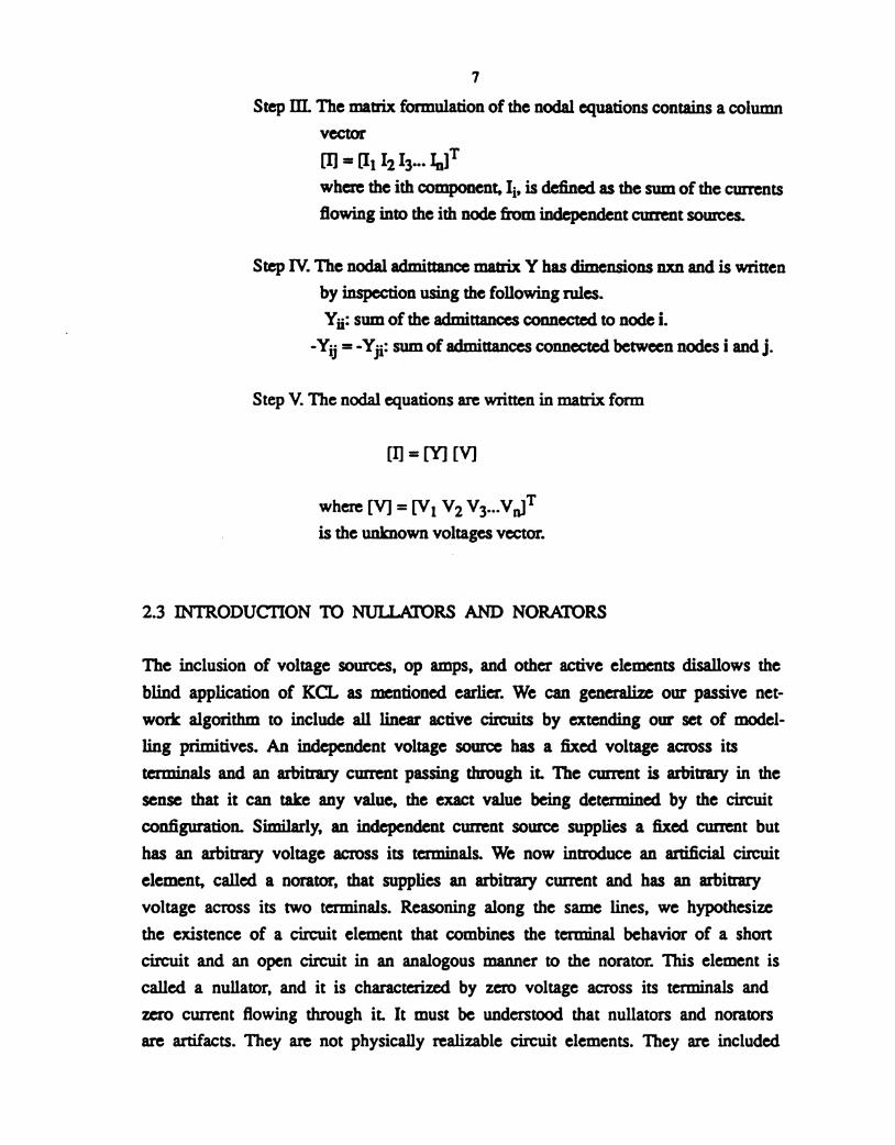
Step H1. The mauix formulation of the nodal equations contains a column
vector
[1] = [11 1213... 1an
where the ith component, Ii, is defined as the sum of the cmrents
flowing into the ith node fiom independent crn'rent somces.
Step IV. The nodal admittance mauix Y has dimensions an and is written
by inspection using the following rules.
Yii: sum of the admittanees connected to node i.
-Yij = -in: sum of admittances connected between nodes i and j.
Step V. The nodal equations are written in mauix form
[I]=[Y][V]
where [V] = [v1 v2 v3...v,,]T
is the unknown voltages vector.
2.3 INTRODUCTION TO NULLATORS AND NORATORS
The inclusion of voltage somces, op amps, and other active elements disallows the
blind application of KCL as mentioned earlier. We can generalize om' passive net-
work algorithm to include all linear active circuits by extending orn' set of model-
ling primitives. An independent voltage source has a fixed voltage across its
terminals and an arbitrary current passing through it. The current is arbiuary in the
sense that it can take any value, the exact value being determined by the circuit
configuration. Similarly, an independent cturent source supplies a fixed current but
has an arbiuary voltage across its terminals. We now inuoduce an artificial circuit
element, called a norator, that supplies an arbiuary current and has an arbiuary
voltage across its two terminals. Reasoning along the same lines, we hypothesize
the existence of a circuit element that combines the terminal behavior of a short
circuit and an open circuit in an analogous manner to the norator. This element is
called a nullator, and it is characterized by zero voltage across its terminals and
zero current flowing through it. It must be understood that nullators and norators
are artifacts. They are not physically realizable circuit elements. They are included
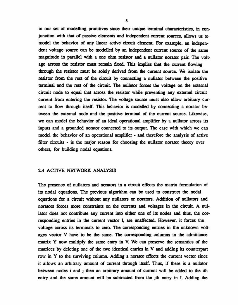
8
in our set of modelling primitives since their unique terminal characteristics, in con-
junction with that of passive elements and independent current sources, allows us to
model the behavior of any linear active circuit element. For example, an indepen-
dent voltage source can be modelled by an independent cmrent source of the same
magnitude in parallel with a one ohm resistor and a nullator norator pair. The volt-
age across the resistor must remain fixed. This implies that the ctnrent flowing
through the resistor must be solely derived from the crurent source. We isolate the
resistor from the mm of the circuit by connecting a nullator between the positive
terminal and the rest of the circuit. The nullator forces the voltage on the external
circuit node to equal that across the resistor while preventing any external circuit
current fiom entering the resistor. The voltage somce must also allow arbiuary cur-
rent to flow through itself. This behavior is modelled by connecting .a norator be-
tween the external node and the positive terminal of the current source. Likewise,
we can model the behavior of an ideal operational amplifier by a nullator across its
inputs and a grounded norator connected to its output. The ease with which we can
model the behavior of an operational amplifier - and therefore the analysis of active
filter circuits - is the major reason for choosing the nullator norator theory over
others, for building nodal equations.
2.4 ACI'IVE NETWORK ANALYSIS
The presence of nullators and norators in a circuit efiects the mauix formulation of
its nodal equations. The previous algorithm can be used to consuuct the nodal
equations for a circuit without any nullators or norators. Addition of nullators and
norators forces more consuaints on the currents and voltages in the circuit. A nul-
lator does not conuibute any current into either one of its nodes and thus, the cor-
responding enuies in the cmrent vector 1, are unafi‘ected. However, it forces the
voltage across its terminals to zero. The corresponding enuies in the unknown volt-
ages vector V have to be the same. The corresponding columns in the admittance
mauix Y now multiply the same entry in V. We can preserve the semantics of the
mauices by deleting one of the two identical enuies in V and adding its counterpart
row in Y to the surviving column. Adding a norator efi‘ects the current vector since
it allows an arbiuary amount of current through itself. Thus, if there is a nullator
between nodes i and j then an arbiuary amount of cmrent will be added to the ith
enuy and the same amount will be subuacted fiom the jth enuy in 1. Adding the
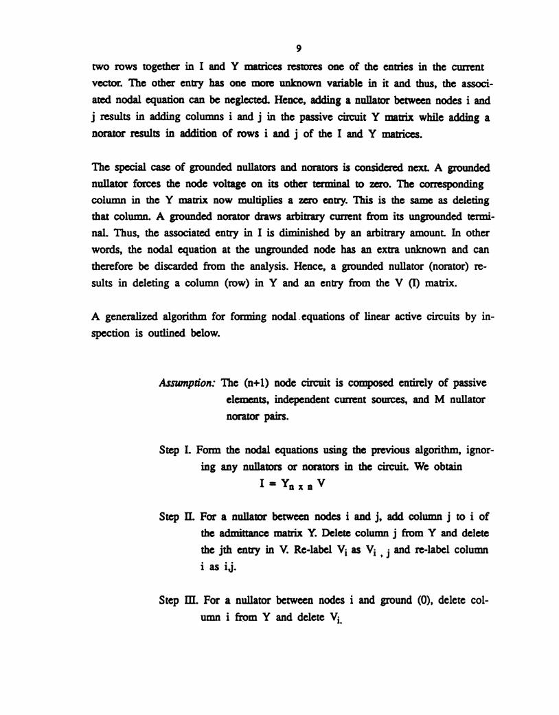
9
two rows together in I and Y mauices restores one of the enuies in the current
vector. The other entry has one more unknown variable in it and thus, the associ-
awd nodal equation can be neglected. Hence, adding a nullator between nodes i and
j results in adding columns i and j in the passive circuit Y mauix while adding a
norator results in addition of rows i andj of the I and Y mauices.
The special case of grounded nullators and norators is considered next. A grounded
nullator forces the node voltage on its other terminal to zero. The corresponding
column in the Y mauix now multiplies a zero enuy. This is the same as deleting
that column. A grounded norator draws arbiuary current from its ungrounded termi-
nal. Thus, the associated entry in I is diminished by an arbiuary amount. In other
words, the nodal equation at the ungrounded node has an exua unknown and can
therefore be discarded from the analysis. Hence, a grounded nullator (norator) re-
sults in deleting a column (row) in Y and an enuy fiom the V (I) mauix.
A generalized algorithm for forming nodal . equations of linear active circuits by in-
spection is outlined below.
Assumption: The (n+1) node circuit is composed entirely of passive
elements, independent ctnrent sources, and M nullator
norator pairs.
Step 1. Form the nodal equations using the previous algorithm, ignor-
ing any nullators or norators in the circuit. We obtain
I = Yn x n V
Step II. For a nullator between nodes i and j, add columnj to i of
the admittance mauix Y. Delete column j from Y and delete
the jth enuy in V. Re-label Vi as Vi , j and re-label column
i as iJ.
Step III. For a nullator between nodes i and ground (0), delete col-
umn i from Y and delete Vi.
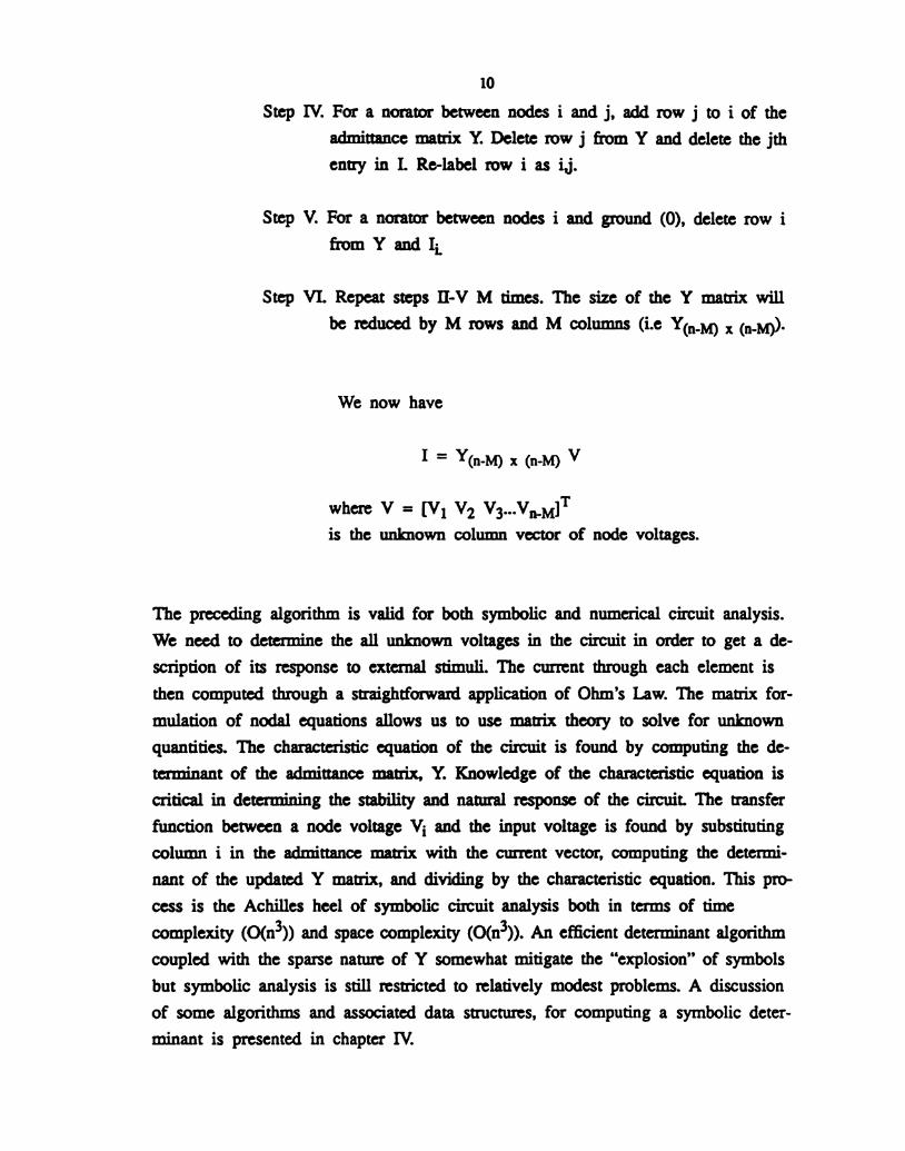
10
SteprForanoratorbetween nodesiandj,addrowjtoiofthe
admittance mauix Y. Delete row j from Y and delete the jth
enuy in I. Re-label row i as i,j.
Step V. For a norator between nodes i and ground (0), delete row i
from Y and Ii.
Step VI. Repeat steps lI-V M times. The size of the Y mauix will
be reduced by M rows and M columns (i.e Y(n,M) x (M4)).
We now have
I = Ytn-M) x (n-M) V
where v = [v1 v2 v3...v,,M]T
is the unknown column vector of node voltages.
The preceding algorithm is valid for both symbolic and numerical circuit analysis.
We need to determine the all unknown voltages in the circuit in order to get a de-
scription of its response to external stimuli. The cmrent through each element is
then computed through a suaightforward application of Ohm’s Law. The mauix for-
mulation of nodal equations allows us to use mauix theory to solve for unknown
quantities. The characteristic equation of the circuit is found by computing the de-
terminant of the admittance mauix, Y. Knowledge of the characteristic equation is
critical in determining the stability and natural response of the circuit. The uansfer
function between a node voltage Vi and the input voltage is found by substituting
column i in the admittance mauix with the current vector, computing the determi-
nant of the updated Y mauix, and dividing by the characteristic equation. This pro-
cess is the Achilles heel of symbolic circuit analysis both in terms of time
complexity (0(n3» and space complexity (0(n3». An efficient determinant algorithm
coupled with the sparse nature of Y somewhat mitigate the “explosion” of symbols
but symbolic analysis is still resuicted to relatively modest problems. A discussion
of some algorithms and associated data su'uctures, for computing a symbolic deter-
minant is presented in chapter IV.
11
2.5 ACTIVE FILTER DESIGN USING SYMBOLIC TRANSFER FUNCTIONS
Sspice is oriented towards active filter design. It is desirable to automate the pro-
cess of detecting filter functions in a circuit and solving for the relevant filter pa-
rameters in terms of circuit parameters. Furthermore, a symbolic estimate of errors
due to non-ideal behavior of circuit parameters is crucial for a designer so that val-
ues of parameters may be chosen to minimize them. An overview of the theory be-
hind second order filters is presented followed by a ueatise on the efi‘ect of finite
Gain-Bandwidth-Product on ideal filter pm'ameters.
We can assume without loss of generality that the input is normalized to one. The
voltage at any node is then just the uansfer function between the node voltage and
the input signal. The denominator of the uansfer function is the characteristic equa-
tion of the circuit. A necessary condition for the existence of second order filter
functions in the circuit is that the frequency domain characteristic equation be of
the form
32 + (wo/Qo)s + W02
where wo is the frequency for which the filter is designed, and the magnitude of
Q0 governs the amplification/attenuation at the frequency wo. The form of the uans-
fer functions’s numerator classifies the filter function at the node as either low-pass,
high-pass, band-pass, natch, or all-pass.
2.5.1 LOW PASS FILTER FUNCTION
A uansfer function that attenuates fiequencies beyond a certain cutofi' frequency wo
but is uansparent to fiequencies below the cutofi’ frequency performs low-pass fil-
tering. For instance, the voltage across the capacitor in a series RC circuit is atten-
uated at high frequencies but is unaffected at low frequencies. A low-pass filter
function is said to exist at the node joining the resistor and the capacitor. A second
order low-pass filter exists at a node if its uansfer function is of the form
H(s) = (HO woz) / ($2 + (“10/on + we?)
It is apparent that at high frequencies the uansfer function behaves like Us2 and at
12
low frequencies it is approximately independent of frequency (i.e H(s) ~ Ho). Thus,
the low frequencies are “passed” at the node while high frequencies are “blocked”.
2.5.2 HIGH PASS FILTER FUNCTION
High-pass filtering is the complement of low-pass filtering. Signals whose frequen-
cies are above a critical frequency are passed unhampered while those whose fre-
quencies are below the cutoff are attenuated. Drawing on the previous example, the
voltage across the resistor in a series CR circuit is attenuated at low fiequencies but
approaches the value of the input signal at high frequencies. The US2 behavior of
the low-pass filter at high frequencies can be counteracted if an s2 is present in the
numerator. This leads to the form of a high-pass, second order filter function
H(s) = (Ho 52) / (32 + (wo/Qo)s + woz)
The magnitude of the uansfer function is approximated by H0 at high fiequencies
and approaches zero at low frequencies. A high-pass filter exists at a node if its
uansfer function has the preceding suucture.
2.5.3 BAND PASS FILTER FUNCTION
Some applications require that only a band of frequencies be uansmitted through a
circuit. For example, a tuner has to recognize a very narrow band of frequencies in
order to “tune” into a particular station. One way of accomplishing this function is
by routing the inconring signal through a filter that allows only a band of frequen-
cies to pass through, and discards the rest of the specu'um. The voltage across the
resistor in a series RLC circuit exhibits band—pass behavior. At low frequencies
most of the voltage is across the capacitor while at high frequencies the inductor
behaves like an Open circuit and thus has most of the voltage across itself. At in-
termediate frequencies the voltage across the resistor increase due to phasor cancel-
lation between the capacitor and inductor voltages. A band-pass filter function
therefore, exists across the resistor. The general form for a second order bandpass
filter is given by
l3
H(s) = (H0 (we/Qua / (s2 + two/Qas + “’02)
The uansfer function is proportional to Us at high frequencies and approaches zero
,at low frequencies. Thus, it behaves like a high-pass filter at low frequencies and
as a low-pass filter at high frequencies. Signals whose frequencies fall around We
areu'ansmittedwithagainofapproximatelwaQointhiscontextcanbeinter-
preted as the selectivity factor (i.e the narrower the band of allowed frequencies,
the higher the Q0).
2.5.4 NOTCH FILTER FUNCTION
A filter that performs the complementary function of a band-pass filter is called a
notch filter. The notch filter can be used to reject unwanted frequency components
in a signal. Applications include removing tape hiss, low frequency rumble from a
record player, et cetera. The second order filter function of a band-pass filter is
H(s) = H0 (s2 + wzz) / (s2 + (wo/Qo)s + woz)
where wz is called the notch frequency. The nOtch filter function may be combined
with high-pass and low-pass filter functions by adjusting the relative magnitudes of
W2 and wo. A we netch filter function results if W2 is equal to wo (i.e. the gain
at frequencies below and above wo are uansmitted without attenuation but a band
of frequencies centered at W0 is “blocked”). Low-pass filtering can be combined
with notch filtering if W0 is less than the notch frequency. The gain at frequencies
below wo is much higher than the high frequency gain in this scenario. Similarly,
notch filtering can be supplemented by high-pass filtering if W0 is greater than wz.
2.5.5 ALL PASS FILTER FUNCTION
It is sometimes desirable to alter the phase of a signal without changing its magni
tude. For example, phase shifts cannot be tolerated when uansmitting data using
Pulse Coded Modulation or a similar coding scheme. A filter that corrects for phase
but leaves the magnitude of the incoming signal unchanged over all frequencies is
14
called an all-pass filter. The only way that the magnitude response can be the same
is if the ratio of the numerator and the denominator of the uansfer function is con-
stant and fiequency independent. However, such a uansfer function does not alter
the phase of the input signal. If we consider a second order filter, we note that the
magnitude of the characteristic equation is unchanged if we flip the sign of the co-
efficient of s]. The phase however changes by 180°. This observation leads to the
general form of a second order all-pass filter
H(s) = Hots2 - (Wo/Qo)s + woz) / (s2 + (wo/Qo)s + woz)
The phase shift is given by
amtan (H(s)) = -2 tan'ttwwo/Qo) I (we2 - win
The filter functions discussed above are based on ideal behavior of circuit compo-
nents. The ideal filter parameters W0 and Q0 represent the design poles of the cir-
cuit’s uansfer functions. The behavior of a filter is particularly sensitive to shifts in
the value of the filter parameters. This problem becomes acute in the case of band-
pass and notch filters since a small change in the value of the center frequency can
cause the filter to miss the intended signal altogether. A shift in Q efiects the se-
lectivity of the filter, usually for the worse. These errors can be minimized if a
closed form estimate in terms of circuit parameters can be found.
2.6 ESTIMATING DEVIANCE IN FILTER PARAMETERS
Sspice analyzes the efi'ect of non-ideal operational amplifier behavior on the design
poles of second order filters. The mativation for focusing on this particular brand
of non-ideality is due to the widespread use of operational amplifiers in active filter
design[2],[3],[6]. An operational amplifier should, theoretically, deliver infinite gain
in a frequency independent manner. In practice, performance degradation starts as
low as 22Hz. An empirical macromodel of an op amp can be obtained through its
frequency response. More poles are introduced into the macromodel as we increase
the frequency of excitation. Adding more poles to the macromodel increases its ac-
curacy but if used in a circuit, causes the number of terms in the symbolic result
to “explode”. It is observed that the conuibution of these poles becomes significant
15
only at very high frequencies. Thus, we can assume a one pole model of an op
amp and successively add more poles into the model as we go higher in fi'equency.
The open loop gain times the frequency at which the first pole becomes significant
is termed as the Gain Bandwidth Product (GBP) of the amplifier. Ideally, the GBP
is infinite. The one pole model of the op amp yields a finite GBP. Inuoducing the
non-ideal model of an op amp causes a shift in the ideal filter parameters W0 and
Q0. Each op amp increases the order of the characteristic equation by one. Howev-
er, the exu'a poles inuoduced into the uansfer function are far fiom the jw-axis and
the behavior of the circuit is dominated by the design poles. The characteristic
equation is therefore, still approximately second order. The effect of the new poles
is to shift the design poles to new values. An estimate of the departure from ideal
W0 and Q0 has been derived by Wilson, Bedri and Bowron[l]. The error estimate
is in terms of circuit parameters. Thus, errors due to finite GBP can be mitigated
by choosing appropriate values of circuit elements. However, it must be remem-
bered that the estimate is valid only as long as the one pole model holds true and
second order and higher error terms can be neglected. As we increase the Operating
frequency, additional modelling must be inuoduced and a new estimate generated to '
minimize the errors in filter parameter values.
CI-IAP'I'ERIII
Numerical Evaluation and Symbolic Approximation
3.1 DRAWBACKS OF SYMBOLIC COMPUTATION
Symbolic computation is often criticized for generating huge suings of symbols that
are hard to analyze and whose physical meaning is obscure. This situation occurs
because symbolic analysis is exact and the conuibution of every parameter, however
insignificant it might be, has to be embodied in the final answer. Moreover, an op-
eration on symbolic operands usually results in an answer whose size is larger than
either one of the Operands. Conuastively, an operation on numeric operands results
in an answer whose representational requirements are comparable to those of the
operands. The numerical value of the result may be larger than either of its oper-
ands but there is no explosion of the representational size (not the value) of the fi-
nal answer. Another galling aspect of symbolic computation is that the time taken
to produce the result depends on the size of input operands. The speed of numeric
computation, on the other hand, is largely independent of the value of input oper-
ands. Symbolic computation is, as. a result, slow and prone to generating irru'actable
results. A suategy is desired that combines the speed and low overhead of numeric
computation with the semantic advantages ofi'ered by symbolic computation to gen-
erate a result that is at once concise and meaningful.
3.2 MTI'IGATING PROBLEMS THROUGH SYMBOLIC APPROXIMATION
Symbolic approximation based on numerical evaluation of circuit parameters is a
methodology to generate symbolic results that are shorter than the exact result but
not as accurate. Frequently, a circuit designer is working on a circuit whose behav-
ior is not apparent through numerical simulation. Moreover, the circuit is such that
its symbolic analysis yields a ponderous result. This situation frequently occurs in
16
l7
macromodelling, where the designer is trying to generate a model that duplicates
the behavior of the circuit. It should be noted that we start with a working circuit
whose circuit parameters have already been defined. We are seeking an understand-
ing of the factors determining circuit behavior. A simpler symbolic result can be
generated if we can ascertain the terms that dominate the final answer. Symbolic
terms whose conuibution to the final result is negligible can be omitted. The sym-
bolic result is not independent of circuit parameter values. That is, there is no guar-
antee that the same set of symbolic terms will be generated if we analyze the
problem with a difierent set of parameter values. However, the insight provided to
the designer about the circuit’s behavior may make such a uade ofi' worthwhile.
Keeping these limitations in mind, a brief outline of a systematic procedure for ap-
proximating the exact symbolic result is presented.
Step I. Read the parameter values from the input file. Parameters that are found
from the DC operating point are obtained from the user.
Step II. Carry out an exact symbolic analysis of the circuit.
Step III. Evaluate each term in the exact answer using the parameter values provid-
ed.
Step IV. The exact symbolic result is a polynomial in the Laplace symbol ‘3’. Each
symbolic coefficient is approximated separately so that the original su'ucture of the
polynomial is preserved. A symbolic coefficient is approximated by comparing the
magnitude of each term in the coefficient with the largest magnitude found in the
group, and neglecting those whose value falls below a certain threshold of the max-
imum value.
Step V. Repeat step IV for each coefficient of si in the polynomial.
The definition of neglect has yet to be elucidated. As mentioned earlier, we neglect
terms whose conuibution to the final result is negligible. A term is deemed negli-
gible if it falls below a certain percentage of the largest term in its group (Step
IV). This threshold is conuolled by the user. A low threshold will result in an ap-
proximated result that is closer to the exact answer than if a high threshold is cho-
sen. The choice of the threshold is thus dependent on the amount of accuracy that

18
is desired. Presently, Sspice uses a Step function to implement symbolic approxima-
tion. (i.e terms whose values are suictly less than the threshold are dropped). A
more naurral approach would be to use some kind of decay function, the decay
constant being left to the user.
CHAPTERIV
Operational Specifics and Salient Features
4.1 BEHAVIORAL DESCRIPTION OF SSPICE MODULES
Sspice is implemented as a set of four programs that can be run separately or un-
der the control of a driver. Each program executes one phase of circuit analysis.
Thus, the first module generates a matrix formulation of nodal equations from an
input file. The second module takes this output and computes the characteristic
equation and various node voltages. The second module, optionally, generates the
input file for the third or fourth module depending on whether ideal filter analysis,
or error estimation is desired by the user. The third module performs ideal filter
analysis on node voltages that are supplied to it as input. The fourth module re-
quires an input file containing the ideal, and first order error terms in the charac-
teristic equation. It estimates the shifts in ideal filter parameters based on this data.
4.2 OVERALL OPERATION
The command Sspice invokes a driver that sequentially invokes processes to exe-
cute the first and second modules, and (optionally) the third or forum module. In
this scenario, the user can only conuol the execution of Sspice but is prohibited
fiom accessing any intermediate data generated by the modules. Intermediate data,
such as the mauix formulation of nodal equations, is stored in temporary files be-
tween successive module invocations. The names of these files, plus some book-
keeping information, is written to another file, called a messenger file. Information
pertaining to the whereabouts of this messenger file is supplied when invoking the
relevant module. Safe names must be generated for these temporary files so that ex—
isting files that are named the same, are not overwritten. This is accomplished
through a set of system calls to the operating system. Beth UNIX and DOS support
19
20
this facility. Furthermore, generating safe names for intermediate files allows multi-
ple invocations of Sspice. Multiple invocations are only possible in a windowing
environment due to the interactive character of Sspice. One cannot easily circum-
vent this feature by writing a batch file, since the number of interactive queries de-
pends on the nature of the response to those queries. The driver checks the exit
status returned by each module for satisfactory completion before continuing execu-
tion. The user is thus, buffered from run time errors arising fi'om an erroneous cir-
cuit description or bugs in the program.
4.3 ERROR DETECITON AND RECOVERY
Each module has one enuy and one exit point. The reason for termination of the
module is returned in the exit status of the process executing it. A non-zero value
signals an abnormal termination of the module. There are two main sources that
cause a module to exit abnormally. Erroneous input data, whether supplied by the
user or by the preceding module, is the foremost reason causing the program to
crash. A less likely, but equally debilitating circumstance arises when some system
imposed limit is exceeded. Other reasons behind abnormal termination include, user
generated software interrupts and logical errors in the code. The resulting signal
generated in each case, is uapped by an error handling routine that removes any
temporary files or data generated by the erring module, and renuns the exit status
to the driver. A message explaining the reason for the abort is written to the
terminal. Error messages caused by bugs in the program are further accompanied by
the line number and function name in which the error occurred. The omission of
floating point exceptions from the discussion might seem as an oversight given the
numerical evaluation feature of Sspice. Special provisions - software checks for
divide-by—zero, argument to square root function, e.t.c - are built into the code so
that such errors never occur. The rationale is that a floating point exception during
numerical analysis should not impede an exact symbolic analysis since Sspice is
predominantly a symbolic analysis package. No such error recovery is possible
when an erroneous description of the circuit topology is detected. For instance, if
one of the resistor terminals has not been specified in the input file then the circuit
is not completely defined and therefore, there is not much point in continuing
execution. By the same token, execution is aborted if a system call returns an error
status. This could occur, most likely, during a dynamic memory allocation call, and
21
perhaps less likely, if an error in file creation is caused due to some pre imposed
limit on the number of simultaneously open files. Thus, considerable effort is
directed towards enforcing a graceful degradation in performance on encountering
pathological situations.
4.4 USER FRIENDLY FEATURES
The user can gain finer conuol over the execution of Sspice if each module is ex-
ecuted separately. This feature allows the user to access and modify temporary data
generated by the modules. Resistors can be removed from the circuit, for example,
by deleting the respective mauix enuies generated by the first module, before run-
ning the second module. The user can also shrink the size of the mauices by using
some heuristics from mauix theory in order to speed up determinant computation.
Determinants containing symbolic enuies can be computed independently of the first
module, a feature that is particularly attractive to conuol theory and mathematics
applications. As a more sophisticated example, consider approximating the exact
symbolic analysis of a circuit topology containing a JFET, resistors and capacitors.
The values of the uansconductance, and the drain to source resistance and capaci-
tance are obtained by calculating the DC operating point at the beginning. However,
these values have to be prompted for during each invocation of Sspice since they
are not Specified in the original SPICE input file. Sspice creates a data file contain-
ing the names of parameters and their corresponding numerical values during the
first analysis of the circuit so that successive invocations can read from it without
prompting the user. A difi‘erent symbolic answer is generated by simply changing
the pmmeter values in this file before the next run. It should be realized that the
flexibility obtained by this feature is prone to malicious use and is thus, inappropri-
ate for the naive user:
4.5 OPERATIONAL DESCRIPTION OF SSPICE MODULES
4.5.1 MODULE I: FORMING NODAL EQUATIONS
The first module generates a mauix formulation of a Circuit’s nodal equations given
its topological description. Sspice accepts input in a format popularized by SPICE
22
so that symbolic analysis and numerical simulation may alternate without interven-
ing editing of the input file. Format compatibility is assured from SPICE to Sspice
but compatibility does nor always hold in the reverse direction. The Sspice input
file format allows much more latitude in element definitions than does SPICE.
Sspice elements of the same type may have identical names, and need not be fol-
lowed by their numerical value. In fact, two symbols are considered equal in a
symbolic sense if their names are the same. A rich element library is supported al-
though the majority of the models can be interpreted as predefined macros that con-
sist of just resistors, capacitors, nullators, norators, and independent current sources.
Multiple models for the same circuit element - distinguished by their degree of
complexity - are available so that the desired level of modelling may be incorpo-
rated in the result. Appendix A lists the complete Sspice element library together
with the format in which each element should appear in the input file. The first
module makes two passes over the input file. The first pass checks to see if the
circuit is fully specified and also establishes an upper bound to the size of the ma-
uices. The space for the I, Y, and V mauices is then dynamically allocated. The
second pass over the input file recognizes, and inserts the appropriate model for,
circuit elements into the mauices. The user is asked to decide between the ideal
and the one pole model if any op amps are encountered in the circuit description.
A flow chart depicting the interactive su'ucture of the first module is given in Ap-
pendix D. The modelling phase is followed by a nullator norator reduction of the
mauices as explained in the first chapter: The resulting mauix formulation is written
to a temporary file and the exit status returned to the driver.
4.5.2 MODULE II: SOLVING NODAL EQUATIONS
The second module computes the determinant of the mauices specified in the input
file and performs a user conuolled level of analysis on the result. The determinant
of the admittance mauix, Y, supplies the characteristic equation. Cramer’s rule can
be used to evaluate other node voltages in the circuit. Each node voltage requires
computing a determinant, and rather than computing all the node voltages, the user
is asked to select those of interest to him/her: This feature avoids time consuming,
and usually unnecessary computation of determinants. Sorting the determinants on
basis of a user supplied key is also supported. The default sorting key is the
Laplace symbol ‘3’. The user is allowed to selectively enable this option for each
23
determinant, since sorting is a time consuming activity. Numerical evaluation of the
symbolic result is another option available to the user: The user is prompted for pa-
rameter values only if the parameter is part Of the answer. These values along with
the corresponding parameter names are saved in an external file at the request of
the user. Subsequent invocations of Sspice that analyze the same circuit can Obtain
the values from this file instead of prompting the user. The user can, Of course, di-
rect the program to ignore the data file when searching for parameter values. Ap-
pendix D charts the sequence of queries output by the program.
A simpler symbolic result can be obtained through the symbolic approximation fea-
ture. Its implementation is relatively straightforward. The exact symbolic answer is
broadly divided into ideal and non ideal terms. Each class Of terms is further
grouped by orders Of the Inplace symbol ‘s’ and each such subgroup is simplified.
Each subgroup consists of a number of terms in sign magnitude form. Associated
with each term is a numeric field that contains the numerical evaluation of the
term. The terms are sorted in decreasing order based on their numerical magnitude
and terms below a certain user conuolled threshold are dropped fiorn the answer.
This procedure is repeated for each subgroup and the results are merged together to
form a simplified answer. The CMOS opamp example in Appendix C spectacularly
illusu'ates this powerful idea. Further analysis (ideal filter analysis or error estima-
tion) of the simplified or exact result is conuolled by the user in which case the
second module writes the result to a temporary file. If no further analysis is desired
the various node voltages and the characteristic equation are written to a file. The
original I, Y, and V mauices are also printed in the output file in conventional ma-
uix format. The mauix printing routine automatically adapts to accommodate differ-
ent sized mauices. Implementing all these features efficiently made the design of
the second module especially challenging. However, the time spent in computing
determinants is the dominant performance statistic Of the second module, and in-
dwd, of Sspice and its implementation is discussed now.
A detailed description Of the algorithm for determinant computation is relevant due
to its decisive role in determining Sspice’s performance. Gaussian elimination and
similar numerical techniques are inappropriate for computing determinant of mauices
with symbolic enuies. These techniques require some measure Of division and
reduction of enuies to zero. Reducing an enuy to zero is an expensive Operation
symbolically for it entails sorting and searching Of terms. Symbolic division is
2A
limited to cancellation of common factors in the numerator and denominator and is
therefore, inefi'ective compared to its numeric counterpart. Computing determinants
based on the definition of the determinant is the key idea behind Sannuti and Ptni’s
method [9], one that has been implemented in Sspice.
Broadly, determinant computation involves generating a set of permutations, multi-
plying out the corresponding entries in the mauix, and cancelling all terms that
have the same magnitude but opposite sign. Unlike terms are cancelled by first sort-
ing terms lexicographically irrespective of their sign, and then searching for a pair
of terms that are lexicographically equal but differ in their first character (i.e. sign).
Generating all the permutations Of the mauix - called Y for the purposes of this
discussion - is both inefficient and unnecessary. Only the non zero permutations are
needed. This can be accomplished by creating another mauix of the same dimen-
sion that contains the locations of the zero enuies in the original mauix. This ma-
trix is termed the routing mauix, R, in [9]. Specifically, each column k in Y maps
to column k in R in the following fashion: The row number of the first non zero
enuy in the Y column vector is the first enuy in the R column vector. Scan the Y
column vector, updating successive enuies in the R column vector with the row
numbers of non zero enuies in Y until either a zero enuy is encountered or the
end of the column is reached. In either case, repeat the procedtue for the k+1 col-
umn. A sparse mauix would result in at least one row of zeros in R. Non zero
permutations can be generated by scanning R. The basic idea is to fix a non zero
enuy in the first column in R and vary non zero enuies in the other columns. This
procedure is repeated for each non zero enuy in the first column. The algorithm
terminates when a zero is encountered. As each permutation is generated, a proce-
dure is called to multiply out the corresponding enuies in Y and append them to a
suing representing the determinant. The algorithm in this form fails for a mauix
that has at least one column consisting entirely of non zero enuies. The correspond-
ing routing mauix has no row of zeros and therefore, the algorithm never termi-
nates. This situation can be remedied by appending a row of zeros after the last
row in R. This simple provision forces the algorithm to work for all mauices. It
should be noted that the routing mauix is now of size (n+1) by (n) assuming that
Y is a square mauix of dimension (n).
4.5.2.1 EXAMPLE
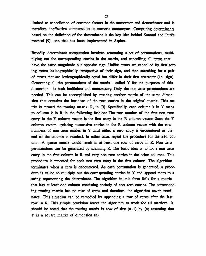
The determinant finding algorithm[9] can best be illusu'ated by an example. Consider the
following upper uiangular mauix, whose determinant is, fiorn mauix theory, the product
Of its diagonal elements. The corresponding routing mauix. R, is also shown.
~G G-l -l l 1 1 1 l
0 -SL 1+sC sL-l . O 2 2 2
O 0 sC G O 0 3 3
O O O ~sL 0 O O 4
Y4x4 R4x4
Vectors F, IS, and P, each of dimension 4, together with an integer variable, k, are also re-
quired by the algorithm. The following table represents an execution uace for generating
the first permutation of the mauix R. The vector, IS, stores the permutation generated.
Table 4.1 Execution uace of determinant algorithm
Step CXOCUIO‘I K le4 Plx4 1S1“
Initialization 1 - [1.0.0.0] [1.1.1.1] [l.*."'.‘
Forward 2 [1.0.0.0] [1.1.1.1] [1.‘."."
Search(l).(2).(4) 2 [1.0.0.0] [1.2.1.1] [l.“.‘.‘
Smh(l).(2).(3) 2 [1.1.0.0] [1.2.1.1] [1.2. .‘l
Forward 3 [1.1.0.0] [1.2.1.1] [1. 2. ‘. ]
Search(l).(2).(4) 3 [1.1.0.0] [1.2.2.1] [1.2. ‘.*]
Search(l).(2).(4) 3 [1.1.0.0] [1.2.3.1] [1.2.". ‘]
Smh(l).(2).(3) 3 [1.1.1.0] [1.2.3.1] [1.2.3 ‘1
Forward 4 [1.1.1.0] [1.2.3.1] [l.2.3."]
Search (1).(2).(4) 4 [1.1.1.0] [1.2.3.2] [1.2.3.‘1
Scarch(1).(2).(4) 4 [1.1.1.0] [1.2.3.3] [1.2.3.‘]
Search (1). (2). (4) 4 [1.1.1, 0] [1.2. 3.4] [1.2.3. ‘1
Search (1).(2).(3) 4 [1.1.1.1] [1.2.3.4] [1.2.3, 4]
Flower(Decodeperrnutation) 3 [1.1.0.0] [1.2.4.1] [1.2.3.4]
Seareh(1).(5) 3 [1.1.0.0] [1.2.4.1] [1.2.3.4]
Backward 2 [1.0.0.0] [1.3.1.1] [1.2.3.4]
Search(l).(5) 2 [1.0.0.0] [1.3.1.1] [1. 2.3, 4]
Backward 1 [0.0.0.0] [2.1.1.1] [1.2.3.4]
Search (1), (5), 115mm 1 [ 0.0.0.0] [2.1.1.1] [1.2.3.4]
26
4.5.3 MODULE III: FILTER FUNCTION IDENTIFICATION
The third module identifies ideal filter functions and solves for filter parameters giv-
en an input file containing the characteristic equation and node voltages. Filter func-
tion identification is implemented by associating the general form of second order
filter functions with the uansfer function at each node and exuacting the relevant
coefficients. Appendix B describes the design of a state variable active filter that
aptly illustrates these principles. Solving for filter parameters usually involves the
limited form of division described previously. Computing the ideal Qo requires tak—
ing a square root of a symbolic operand. This is achieved by exuacting simple fac-
tors from the operand and searching it for two occurrences of the same simple
factor. Numerical evaluation of filter parameters is also supported. Circuit parameter
values are obtained from the messenger file. It is possible that a divide-by—zero ex-
ception may occur while calculating the numerical value of filter parameters. It is
desirable. in this situation. to abort numerical evaluation but to continue with the
exact symbolic analysis. Therefore, a variety of software checks are implemented
that detect and prevent such an exception fiom occmring.
4.5.4 MODULE IV: ESTIMATING DEVIANCE DUE TO NON IDEAL EFFECTS
The fourth module estimates the first order errors in ideal filter parameters due to
finite gain bandwidth product of op amps. The error estimate is in terms of circuit
parameters and is based on the Wilson Bedri Bowron approximation [1]. The sym-
bolic value for ideal Q0 and F0 are also computed as a reference. The design of a
state variable active filter in Appendix B analyzes non ideal efi'ects on filter param-
eters using these ideas. Numerical evaluation of the errors and the ideal filter pa-
rameters is implemented in accordance with previous modules. Matching the GBPs
of difl’erent op amps results in a simpler formula for the error estimate. The user
is provided with an option to equate. symbolically, the various GBPs in the answer.
The fourth module is almost entirely built on the code fi'orn the first three modules.
It is expected that future code development will follow the same uend.
27
4.6 CONCLUSION
Considerable effort has been directed towards making 85pice reliable and easy to
maintain. The code, though extensive. is simple and highly portable. There are no
inherent limits to the size of internal data structtnes due to the nanne of symbolic
computation. The size of the problems it can analyze is limited only by the com-
putational resorn'ces available to it. Its implementation in ‘C’ results in high perfor-
mance coupled with small native code. The microcomputer version occupies less
than 150KandanalyzestheexampleinAppendixCinapproximatelyfifteensec—
onds. An aggressive advertizing campaign targeted at both academe and indusuy
may expose a wider audience to a systematic approach to analog circuit design.

CHAPTERV
Future Directions
A symbolic stability analysis of the circuit fi-om its characteristic equation would be
a useful addition to Sspice. An algorithm for implementing this feature is described
in [11]. The approach is eminently feasible since it requires computing a number of
determinants of sparse mauices, a feature that is already implemented in Sspice.
The enuies in the mauices are the symbolic coefficients of the characteristic equa-
tion that is computed in the second module. A stability analysis would result in an-
other set Of consuaints on circuit parameter values and would ofi‘er valuable insight
into circuit behavior.
Symbolic sensitivity analysis is yet another feattne that can be implemented on a
short term basis. Sensitivity analysis is based on an association of terms from the
characteristic equation according to a set of well defined rules. A formula in terms
of circuit parameters for estimating sensitivity to variations in a certain circuit pa-
rameter yields a set of consuaints a circuit designer should be aware of.
The symbolic approximation feature of Sspice is still in a state of infancy. The cru-
rent implementation discards symbolic terms from the can result based on compar-
ison of relative magnitudes, ignoring the sign of each term. altogether. This
approach might fail for a combination of parameter values that should result in a
cancellation of terms that have large. equal magnitudes but Opposite signs. Terms
with smaller magnitude should then. become significant. However. this intelligence
is not incorporated in the current version with the result that an erroneous result
might be generated. Such situations were not encountered during the extensive test-
ing of the software. However. a further refinement is necessary if only for the sake
of completeness.
ZNAP is a software tool that automatically performs Op Amp Relocation on a seed
28

29
circuit and retains only stable configurations of relocated circuits [12]. A major step
towards computer aided active filter design would be to integrate ZNAP with Sspice
in a master slave relationship. It is envisioned that ZNAP would invoke multiple in-
stances of Sspice so that each stable configuration may be symbolically analyzed in
parallel.
Major portions of Sspice are amenable to parallel computation. For instance. all the
permutations of the admittance mauix can be generated in parallel. Similarly. nu-
merical evaluation of terms dtuing symbolic approximation can proceed indepen-
dently of each other. A parallelizing compiler or a rewrite in a parallel language
such as Occam would allow Sspice to analyze a new. larger class of problems.
Symbolic analysis combined with symbolic approximation seems to be the correct
approach. in principle, to analog circuit design. In practice, it requires extensive
computer resources to produce a uactable result.

APPENDICES
APPENDIX A
Input format and modelling of Sspice elements
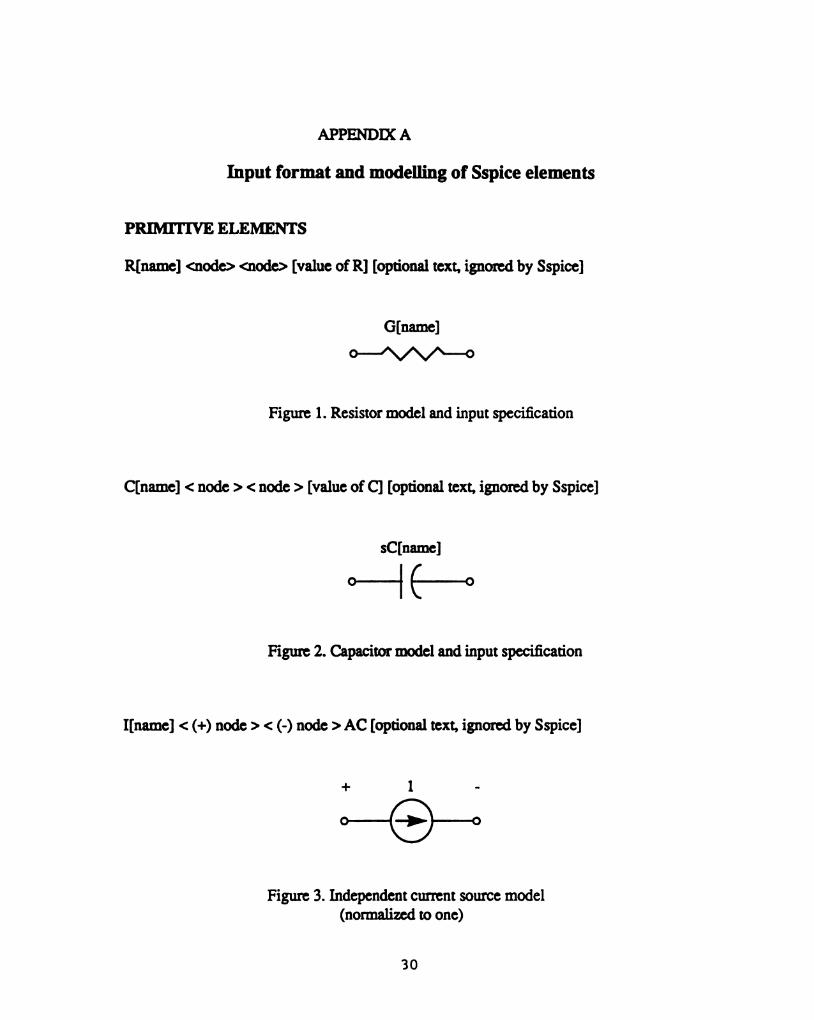
PRIMI'TIVE ELEMENTS
R[name] <node> <node> [value of R] [optional text, ignored by Sspice]
G[name]
o—J\/\/\—o
Figure l. Resistor model and input specification
C[name] < node > < node > [value of C] [Optional text. ignored by Sspice]
sC[name]
o—Ie—e
Figure 2. Capacitor model and input specification
I[name] < (+) node > < (-) node > AC [optional text, ignored by Sspice]
Figure 3. Independent ctnrent source model
(normalized to one)
30
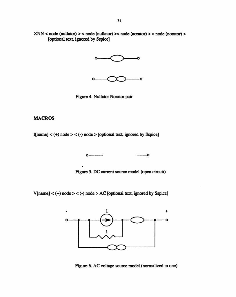
31
XNN < node (nullator) > < node (nullator) >< node (norator) > < node (norator) >
[optional text. ignored by Sspice]
O—O——O
ce—oo—o
Figme 4. Nullator Norator pair
MACROS
I[name] < (+) node > < (-) node > [optional text. ignored by Sspice]
Figme 5. DC current source model (open circuit)
V[name] < (+) node > < (-) node > AC [optional text, ignored by Sspice]
Figure 6. AC voltage source model (normalized to one)
32
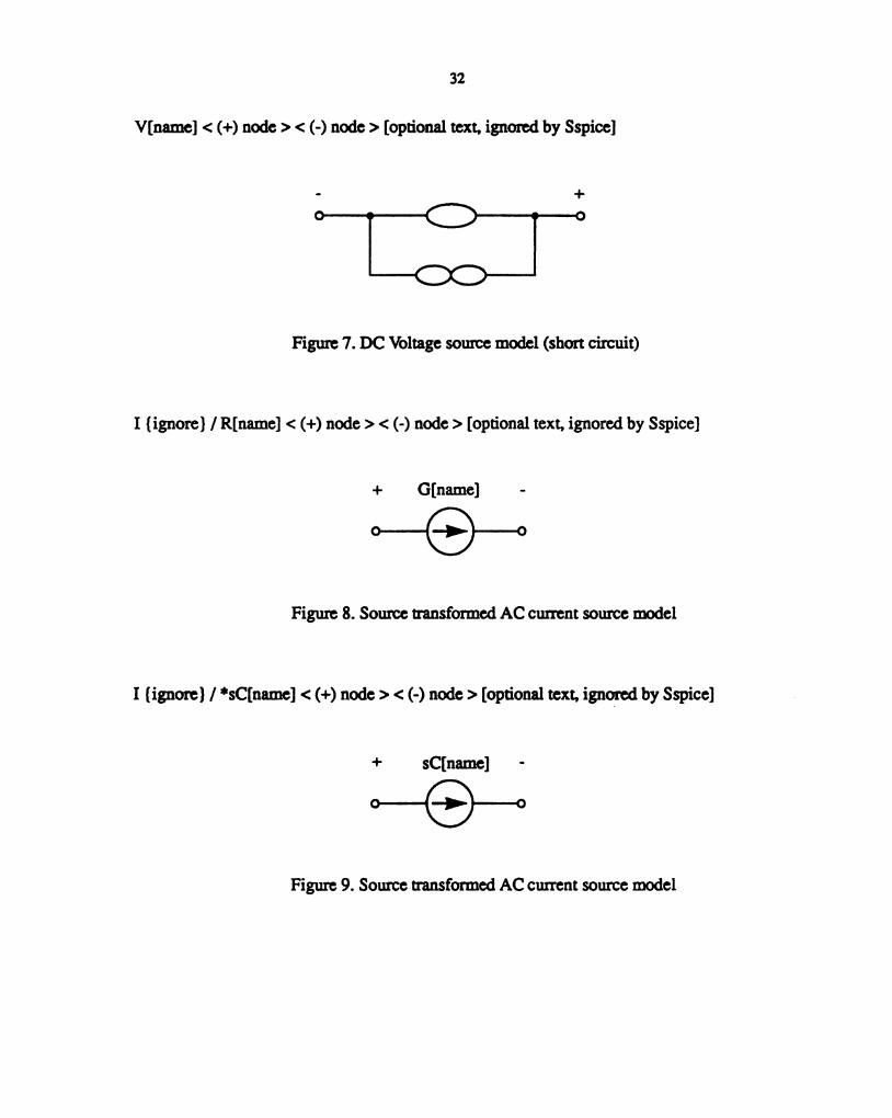
V[name] < (+) node > < (-) node > [optional text, ignored by Sspice]
Figure 7. DC Voltage somce model (short circuit)
I {ignore} / R[name] < (+) node > < (-) node > [Optional text. ignored by Sspice]
+ G[name] -
Figure 8. Source uansformed AC current source model
I {ignore} / *sC[name] < (+) node > < (-) node > [optional text, ignored by Sspice]
+ sC[name] -
Figure 9. Source transformed AC current source model
33
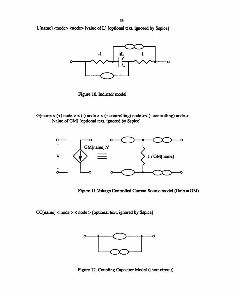
L[name] <node> <node> [value of L] [Optional text. ignored by Sspice]
Figure 10. Inductor model
G[name < (+) node > < (-) node > < (+ controlling) node >< (- conuolling) node >
[value of GM] [Optional text, ignored by Sspice]
o...— e
+
GM[name].V
v —
.;__ .
Figme 11.Voltage Conuolled Current Source model (Gain = GM)
CC[name] < node > < node > [optional text, ignored by Sspice]
Figure 12. Coupling Capacitor Model (short circuit)
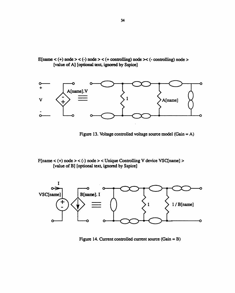
E[name < (+) node > < (-) node > < (+ conuolling) node x (- conuolling) node >
[value Of A] [optional text, ignored by Sspice]
3— - - O o- O -
A[name].V . .
V —— 1 A[name] .
<3— - - O o - 0
Figure 13. Voltage controlled voltage somce model (Gain = A)
F[name < (+) node > < (-) node > < Unique Conuolling V device VSC[name] >
[value of B] [optional text, ignored by Sspice]
I
VSC[name]
+
Figure 14. Current conuolled current source (Gain = B)
35
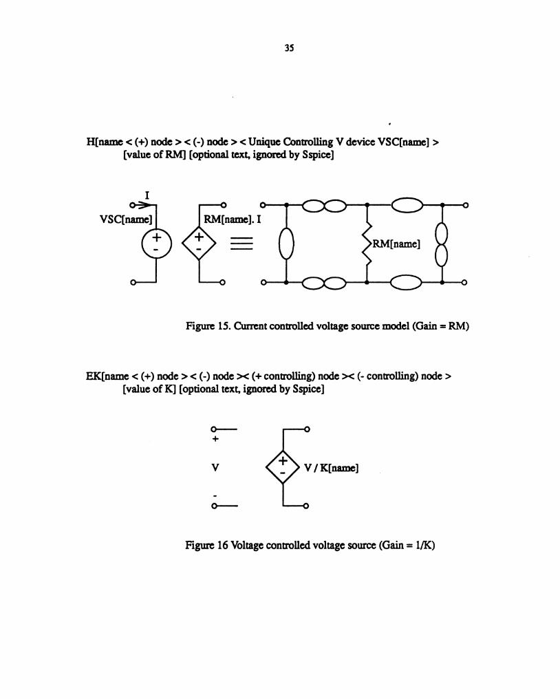
H[name < (+) node > < (-) node > < Unique Conuolling V device VSC[name] >
[value of RM] [Optional text. ignored by Sspice]
I
VSC[name] RM[name]. I
e O E RM[name]
Figure 15. Current conuolled voltage source model (Gain = RM)
EK[name < (+) node > < (-) node X (+ conuolling) node >< (- conuolling) node >
[value of K] [optional text, ignored by Sspice]
our-— 0
+
V 0 V/ K[name]
o_- 0
Figure 16 Voltage conuolled voltage source (Gain = UK)
36
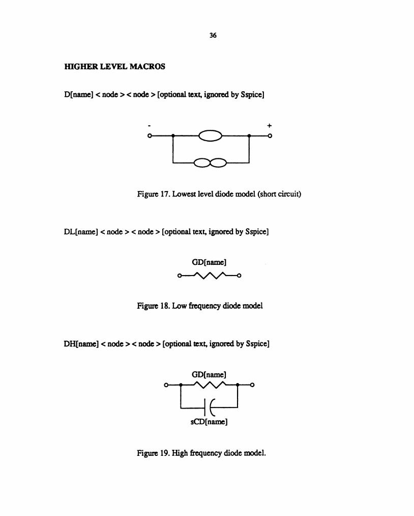
HIGHER LEVEL MACROS
D[name] < node > < node > [Optional text, ignored by Sspice]
Figure 17. Lowest level diode model (short circuit)
DL[name] < node > < node > [optional text. ignored by Sspice]
GD[name]
W0
Figure 18. Low fiequency diode model
DH[name] < node > < node > [optional text, ignored by Sspice]
GD[name]
.___|
sCD[name]
Figure 19. High frequency diode model.
37
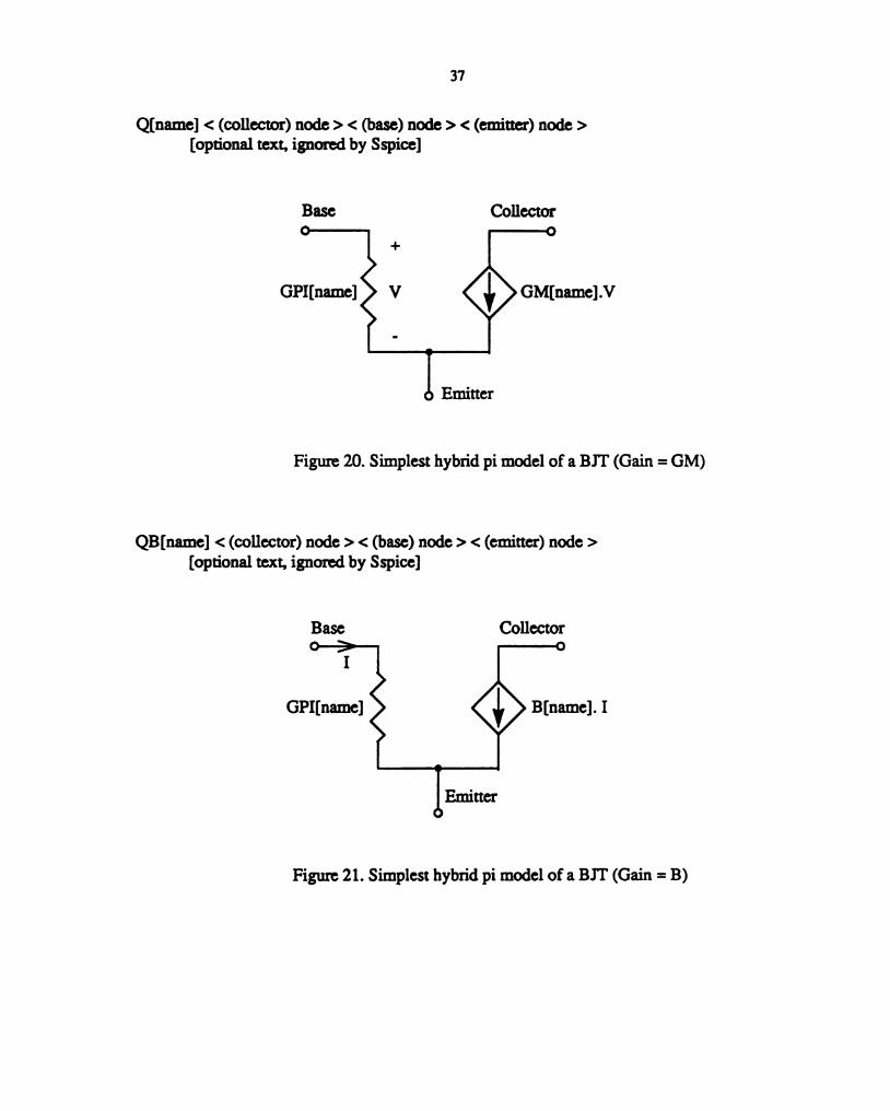
Q[name] < (collector) node > < (base) node > < (emitter) node >
[optional text, ignored by Sspice]
Collector
GPI[name]Basc\/%+1;(:h:[name].V
lEmitter
Figure 20. Simplest hybrid pi model of a BIT (Gain = GM)
QB[name] < (collector) node > < (base) node > < (emitter) node >
[optional text, ignored by Sspice]
Base Collector
I
GPI[name] B[name]. I
Figure 21. Simplest hybrid pi model of a BIT (Gain = B)
38
QL[name] < (collector) node > < (base) node > < (emitter) node >
[optional text. ignored by Sspice]
Base Collector
4
+
GO[name]
GPI[name] V 0 GM[name]
Emitter
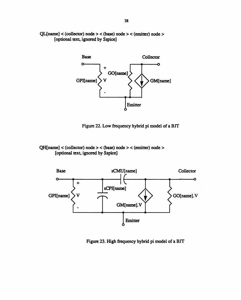
Figure 22. Low frequency hybrid pi model of a BIT
QH[name] < (collector) node > < (base) node > < (emitter) node >
[optional text, ignored by Sspice]
Base sCMU[name] Collector
Ir - - a+ l \
sCPI[name]
GPI[name] V —_ GO[name].V
_ l GM[name].V
lEmrtter
Figure 23. High fiequency hybrid pi model of a BIT
39
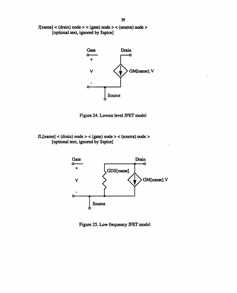
I[name] < (drain) node > < (gate) node > < (source) node >
[optional text. ignored by Sspice]
Gate Drain
0‘_ e
4..
Figure 24. Lowest level JFET model
IL[name] < (drain) node > < (gate) node > < (source) node >
[optional text, ignored by Sspice]
Gate Drain
O— , c
+ cos[name]
v 0 GM[name].V
C - -
I Source
Figure 25. Low frequency IFET model
4o
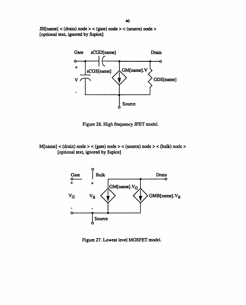
IH[name] < (drain) node > < (gate) node > < (source) node >
[optional text, ignored by Sspice]
Gate sCGD[name]
+ C(}S[nalne]0GM[IIEIDC].V
VT GDS[name]
Source
Figure 26. High frequency JFET model.
M[name] < (drain) node > < (gate) node > < (source) node > < (bulk) node >
[optional text, ignored by Sspice]
GM[name]-VG
GMB[name]-VB
lSource
Gate
Figure 27. Lowest level MOSFET model.
41
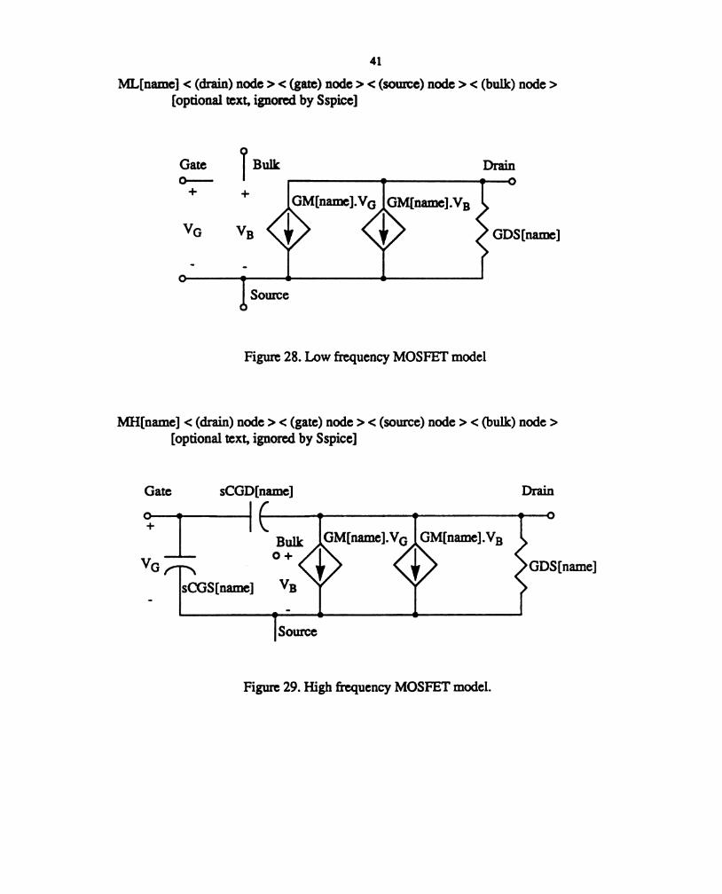
ML[name] < (drain) node > < (gate) node > < (source) node > < (bulk) node >
[optional text, ignored by Sspice]
Bulk Drain
- - fie
GM[name].VG GM[name].V];
B GDS[name]
Gate T
o.__
+ +
VG V
on I
I Source
Figure 28. Low frequency MOSFET model
MH[name] < (drain) node > < (gate) node > < (source) node > < (bulk) node >
[Optional text, ignored by Sspice]
Gate sCGD[name] Drain
i. if ‘ ‘ ‘ °Bulk GM[name].VG GM[name].V};
—— o +
VG /\ ' 0 0 GDS[name]
sCGS[name] VB
[Somce
Figure 29. High fiequency MOSFET model.
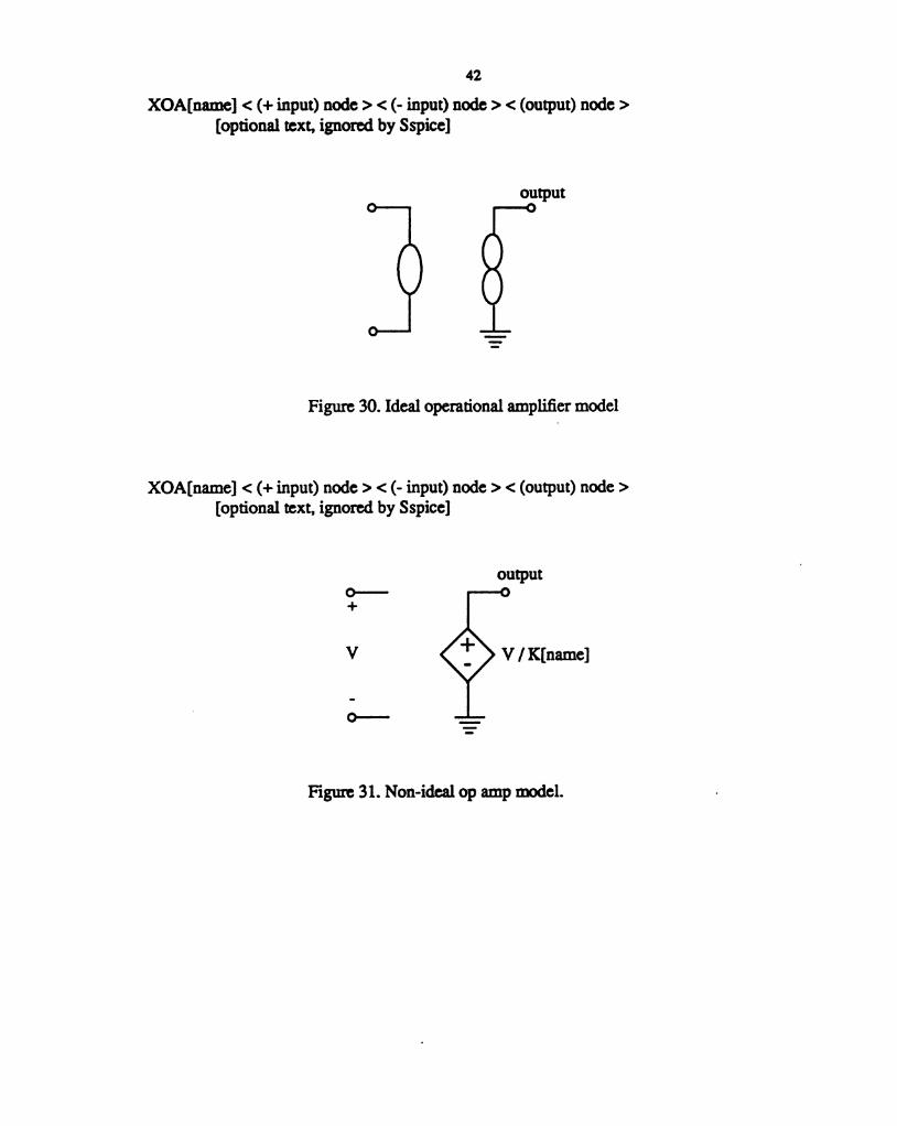
42
XOA[name] < (4» input) node > < (- input) node > < (output) node >
[optional text, ignored by Sspice]
output
Figure 30. Ideal operational amplifier model
XOA[name] < (+ input) node > < (- input) node > < (output) node >
[Optional text, ignored by Sspice]
output
(F .
+
v 6 V/K[name]
[,__
Figme 31. Non-ideal op amp model.
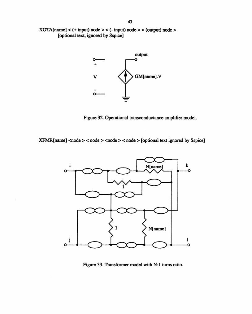
43
XOTA[name] < (+ input) node > < (- input) node > < (output) node >
[optional text. ignored by Sspice]
output
(>— O
+
V 0 GM[name].V
5—
Figure 32. Operational uansconductance amplifier model.
XFMR[name] <node > < node > <node > < node > [optional text ignored by Sspice]
—-OO-—Ii N k
°—-t .. - r—W-n tr—°
1 - I
O o-
O- ..
N[name]
j 1
0—4 - O- - t-——o
Figure 33. Transformer model with N:l turns ratio.
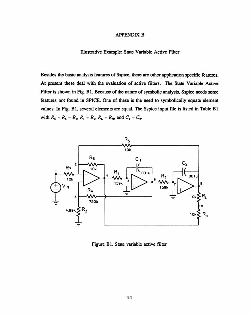
APPENDD{ B
Illusuative Example: State Variable Active Filter
Besides the basic analysis features of Sspice, there are other application specific features.
At present these deal with the evaluation of active filters. The State Variable Active
Filter is shown in Fig. B1. Because of the nature of symbolic analysis. Sspice needs some
features not found in SPICE. One of these is the need to symbolically equate element
values. In Fig. B1, several elements are equal. The Sspice input file is listed in Table Bl
with R, = R6 = R7. R1 = R2. RL = R”, and C1: C2.
R5
NW10k
R5 C1
R ZtF—M—t ll C2
1 7 10“ R l\ I/
} 4 1 '00” R2 “.oom10k t—JVVV
159.. 5 >“—'w»—« a
V'" R 1+ 159k '
4 -
sic—NW } - -: 10“ RI.
: 750k
9
4.99It R3 10k R
H
Figure Bl. State variable acrive filter
44
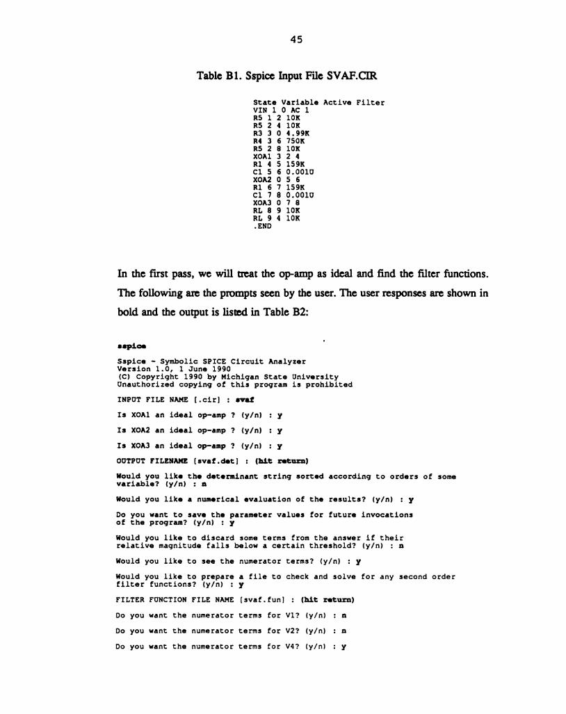
45
Table Bl. Sspice Input File SVAF.CIR
State Variable Active Filter
VIN l 0 AC 1
RS 1 2 10K
R5 2 4 10K
R3 3 0 4.99K
R4 3 6 750K
R5 2 8 10K
XOAl 3 2 4
R1 4 5 159K
C1 5 6 0.0010
XOAZ 0 5 6
R1 6 7 159K
C1 7 8 0.0010
XOA3 0 7 8
RL 8 9 10K
RL 9 4 10K
.END
In the first pass. we will mm the Op-amp as ideal and find the filter functions.
The following are the prompts seen by the user. The user responses are shown in
bold and the output is listed in Table 32:
sepia.
Sspice - Symbolic SPICE Circuit Analyzer
Version 1.0, 1 June 1990
(C) Copyright 1990 by Michigan State University
Unauthorized copying of this program is prohibited
INPUT FILE NAME [.cir] : eve:
Is XOAI an ideal op-amp ? (y/n) : y
Is XOAZ an ideal Op-amp ? (y/n) : y
Is XOAJ an ideal Op-amp ? (y/n) : y
OUTPUT FILENAHE [svaf.detl : (hit return)
Would you like the determinant string sorted according to orders of some
variable? (y/n) : n
Would you like a numerical evaluation of the results? (y/n) : y
DO you want to save the parameter values for future invocations
of the program? (y/n) : y
Would you like to discard some terms from the answer if their
relative magnitude falls below a certain threshold? (y/n) : n
Would you like to see the numerator terms? (y/n) : y
Would you like to prepare a file to check and solve for any second order
filter functions? (y/n) : y
FILTER FUNCTION FILE NAME [svaf.fun] : (bit return)
Do you want the numerator terms for V1? (y/n) : n
DO you want the numerator terms for V2? (y/n) : n
00 you want the numerator terms for V4? (y/n) : y
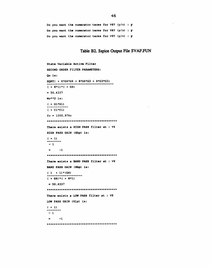
46
Do you want the numerator terms for V6? (y/n) : y
00 you want the numerator terms for V8? (y/n) : y
Do you want the numerator terms for V9? (y/n) : y
Table 82. Sspice Output File SVAFFUN
State Variable Active Filter
SECOND ORDER FILTER PARAMETERS:
00 is:
SQRT{ + 4*64*G4 + 8*G4*63 + 4*63*G3)
( + 6*1)*( + 64)
- 50.4337
Wo**2 is:
( + Gl’Gl)
( + C1*Cl)
fo - 1000.97Hz
tittittttitttfittittttiitttttttiitttttttt
There exists a HIGH PASS filter at : V4
HIGH PASS GAIN (th) is:
i*itttiitfit.tit...tittiflfitiifiiitittiiiif
There exists a BAND PASS filter at : V6
BAND PASS GAIN lab?) is:
( 1 + 1)*(G4)
( + G4)*( + 6‘1)
- 50.4337
flitiii.t*ttittiffittflfifiifitfitiitififlitifiiifi
There exists a LOW PASS filter at : V8
LOW PASS GAIN (Hlp) is:
*flittttittfittfltifiiitttflitiitiitttttitttt
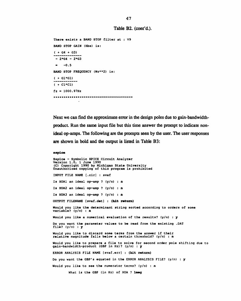
47
Table BZ. (cont’d.).
There exists a BAND STOP filter at : V9
BAND STOP GAIN (Hbs) is:
( + G4 + GB)
- 2*G4 - 2*G3
- -0.5
BAND STOP FREQUENCY (Wz**2) is:
( + 61*61)
( + C1*Cl)
fz - 1000.973:
*ittfittfifiiitittitii*tititttttttttttiiiit
Next we can find the approximate error in the design poles due to gain-bandwidth-
product. Run the same input file but this time answer the prompt to indicate non-
ideal op-amps. The following are the prompts seen by the user. The user responses
are shown in bold and the output is listed in Table B3:
aepice
Sspice - Symbolic SPICE Circuit Analyzer
Version 1.0, 1 June 1990
(C) Copyright 1990 by Michigan State University
Unauthorized copying of this program is prohibited
INPUT FILE NAME [.cir] : svaf
Is XOAl an ideal op-amp ? (y/n) : n
Is XOA2 an ideal op-amp ? (y/n) : n
Is XOA3 an ideal op-amp ? (y/n) : n
OUTPUT FILENAME [sva£.det] : (hit return)
Would you like the determinant string sorted according to orders of some
variable? (y/n) : n
Would you like a numerical evaluation of the results? (y/n) : y
Do you want the parameter values to be read from the existing .DAT
file? (y/n) : y
Would you like to discard some terms from the answer if their
relative magnitude falls below a certain threshold? (y/n) : n
Would you like to prepare a file to solve for second order pole shifting due to
gain-bandwidth-product (GBP in Hz)? (y/n) : y
ERROR ANALYSIS FILE NAME [svaf.errl : (hit return)
Do you want the GBP's equated in the ERROR ANALYSIS FILE? (y/n) : y
Would you like to see the numerator terms? (y/n) : n
What is the GBP (in Hz) of XOA ? lmeg
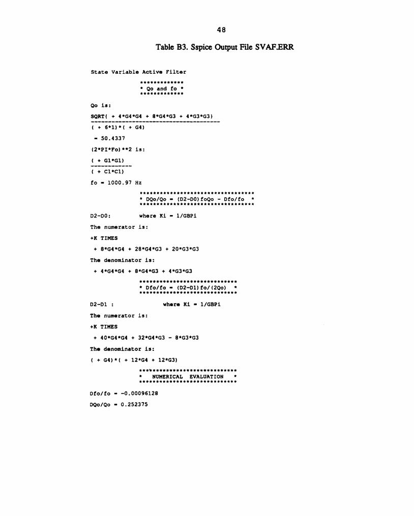
48
Table B3. Sspice Output File SVAFERR
State Variable Active Filter
*ttitttttfliti
* Go and fo *
*tittttttittt
Go is:
SQRT( + 4*G4*G4 + 8*G4*G3 + 4*GB*G3}
( + 6*1)*( + Gd)
- 50.4337
(2*PI*Fo)**2 is:
( + 61*61)
( + C1*C1)
fo - 1000.97 Hz
tittiitttitititifittttttiitttttttt
* DOo/Qo - (DZ-D0)foQo - Dfo/fo *
*tiitkittfiittittttttt*ttttttfitttit
DZ-DO: where Ki - l/GBPi
The numerator is:
+K TIMES
+ 8*G4'G4 + 28*G4*63 + 20*G3*G3
The denominator is:
+ 4*G4*64 + 8*G4*G3 + 4*63*Ga
*ittitiitttttitttttttttttitit
* Dfo/fo - (DZ-Dllfo/(ZQO) *
tittflfittiii*tififliiifit**fl**tit
D2-Dl : where Ki - 1/GBPi
The numerator is:
+t< trues
+ 40*G4*G4 + 32*G4*GB - 8*G3'G3
The denominator is:
( + G4)*( + 12*G4 + 12*63)
itthfiiiitititititttitfittiiiit
* NUMERICAL EVALUATION *
t.fitifii*tfifiittitiititiittittt
Dfo/fo - -0.00096128
DQo/Qo - 0.252375
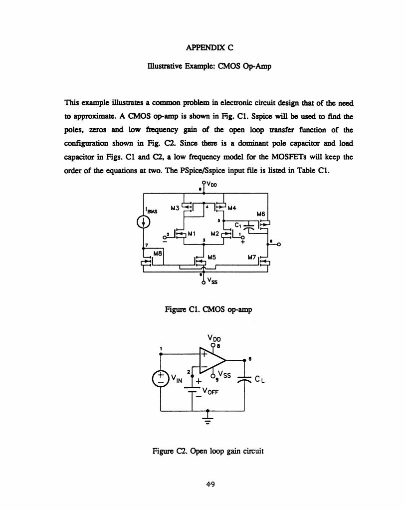
APPENDIX C
Illustrative Example: CMOS Op—Amp
This example illustrates a common problem in electronic circuit design that of the need
to approximate. A CMOS op-amp is shown in Fig. C1. Sspice will be used to find the
poles, zeros and low frequency gain of the open loop transfer function of the
configuration shown in Fig. C2. Since there is a dominant pole capacitor and load
capacitor in Figs. C1 and C2, a low frequency model for the MOSFETs will keep the
order of the equations at two. The PSpice/Sspice input file is listed in Table C1.
Von
I
M3 ‘El—Jfiié' M4'eus M6
5
swam . web:
7
M8 M5 M7 I
E“ ._L._.
Figure C2. Open loop gain circuit
49
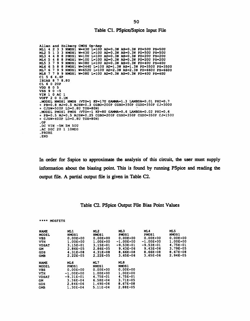
5C)
Table C1. PSpice/Sspice Input File
Allen and Holberg CMOS Op-Amp
MLl 4 2 3 3 NMOSl W-43U L-lOU AD-0.3N As-0.3N PD-SOU Ps-SOU
MLZ 5 l 3 3 NMOSl W-43U L-1OU AD-0.3N As-0.3N PD-SOU Ps-SOU
ML3 4 4 8 8 PMOSl w-IOU L-lOU AD-0.3N AS-0.3N PD-ZOU Ps-20U
ML4 5 4 8 8 PMOSl w-100 L-lOU AD-0.3N As-0.3N PD-ZOU Ps-20U
MLS 3 7 9 9 NMOSl W-380 L-10U AD-0.3N As-0.3N PD-40U Ps-4OU
ML6 6 5 8 8 PMOSI W-344U L-lOU AD-1.3N AS-1.3N PD-3SOU PS-JSOU
ML? 6 7 9 9 NMOSl W-GSZU L-lOU AD-2.3N AS-2.3N PD-660U Ps-66OU
ML8 7 7 9 9 NMOSI W-380 L-lOU AD-0.3N As-0.3N PD-4OU Ps-4OU
Cl 5 6 4.4P
IBIAS 8 7 8.80
CL 6 0 20P
VDD 8 0 S
V33 9 0 -S
VIN 1 0 ac 1
vorr 2 o 0.1M
.MODEL NMOSl unos (VTO-l KP-17U sauna-1.3 LAMBDA-0.01 par-0.7
+ PB-0.8 MJ-0.S MJSW-0.3 CGBO-ZOOP ccso-3509 coco-3509 CJ-300U
+ CJSWuSOOP LD-0.8U rox-aoN) '
.MODEL PMOSl PMOS (vro--1 KP-8U GAMMA-0.6 LAMBDA-0.02 PHI-0.6
+ PB-0.S MJ-o.s MJSW-0.25 CGBO-ZOOP ccso-ssoa capo-3509 CJ-lSOU
+ CJSW-400P LD-0.8U TOX-BON)
.0?
.oc vrn -5M SM 500
.AC DEC 20 1 10MEG
.PROBE
.END
In order for Sspice to approximate the analysis of this circuit, the user must supply
information about the biasing point. This is found by running PSpice and reading the
output file. A partial output file is given in Table C2.
Table (:2. PSpice Output File Bias Point Values
**** MOSFETS
NAME ML1 ML2 ML3 ML4 MLS
MODEL NMOSl NMOSI PMOSI PMOSI NMOSI
VBS 0.00E+00 0.00E+00 0.00E+00 0.00E+00 0.00E+00
VTH 1.00E+00 1.00E+00 -1.00E+00 -1.00E+00 1.00E+00
VDSAT 3.15E-01 3.158-01 -9.53E-01 -9.53E-01 4.75E-01
GM 2.86E-05 2.86E-05 9.438-06 9.43E-06 3.79E-05
GDS 4.3lE-08 4.318-08 8.66E-08 8.66E-08 8.67E-08
GMB 2.22E-05 2.223‘05 3.65E-06 3.6SE-06 2.948-05
NAME ML6 ML7 ML8
MODEL PMOSl NMOSl NMOSl
VBS 0.00E+00 0.00E+00 0.00E+00
VTH -1.00E+00 1.00E+00 1.00E+00
VDSAT -9.31E-01 4.7SE-01 4.7SE-01
GM 3.36E-04 6.58E-04 3.71E-05
GDS 2.84E-06 1.49E-06 8.678-08
6MB 1.30E-04 5.118-04 2.88E-05
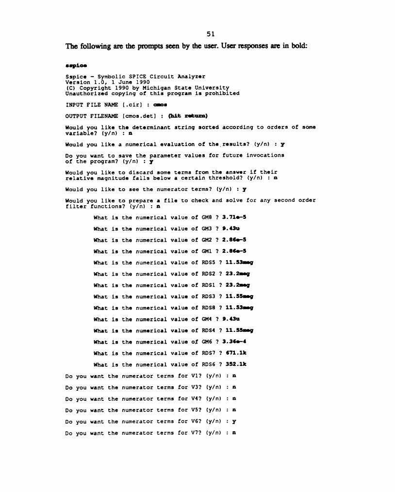
5 1
The following are the prompts seen by the user. User responses are in bold:
eepice
Sspice - Symbolic SPICE Circuit Analyzer
Version 1.0, 1 June 1990
(C) Copyright 1990 by Michigan State University
Unauthorized copying of this program is prohibited
INPUT FILE NAME [.cir] : cane
OUTPUT FILENAME [cmos.det] : (hit return)
Would you like the determinant string sorted according to orders of some
variable? (y/n) : n
Would you like a numerical evaluation of the results? (y/n) : 3
Do you want to save the parameter values for future invocations
of the program? (y/n) : y
Would you like to discard some terms from the answer if their
relative magnitude falls below a certain threshold? (y/n) : n
Would you like to see the numerator terms? (y/n) : y
Would you like to prepare a file to check and solve for any second order
filter functions? (y/n) : n
What is the numerical value of GM8 ? 3.71e-5
What is the numerical value of GM3 ? 9.43u-
What is the numerical value of GMZ ? 2.86e—5
What is the numerical value of GMl ? 2.86e-5
What is the numerical value of RDSS ? 11.53meg
What is the numerical value of R082 ? 23.2:eg
What is the numerical value of R051 ? 23.2-eg
What is the numerical value of RDS3 ? 11.55meg
What is the numerical value of R058 ? 11.53meg
What is the numerical value of GM4 ? 9.43u
What is the numerical value of RDS4 ? 11.55meg
What is the numerical value of GM6 ? 3.36e-4
What is the numerical value of RDS7 ? 671.1k
What is the numerical value of R036 ? 352.1k
Do you want the numerator terms for V1? (y/n) : n
Do you want the numerator terms for V3? (y/n) : n
Do you want the numerator terms for V4? (y/n) : n
Do you want the numerator terms for V5? (y/n) : n
Do you want the numerator terms for V6? (y/n)
Do you want the numerator terms for V7? (y/n)
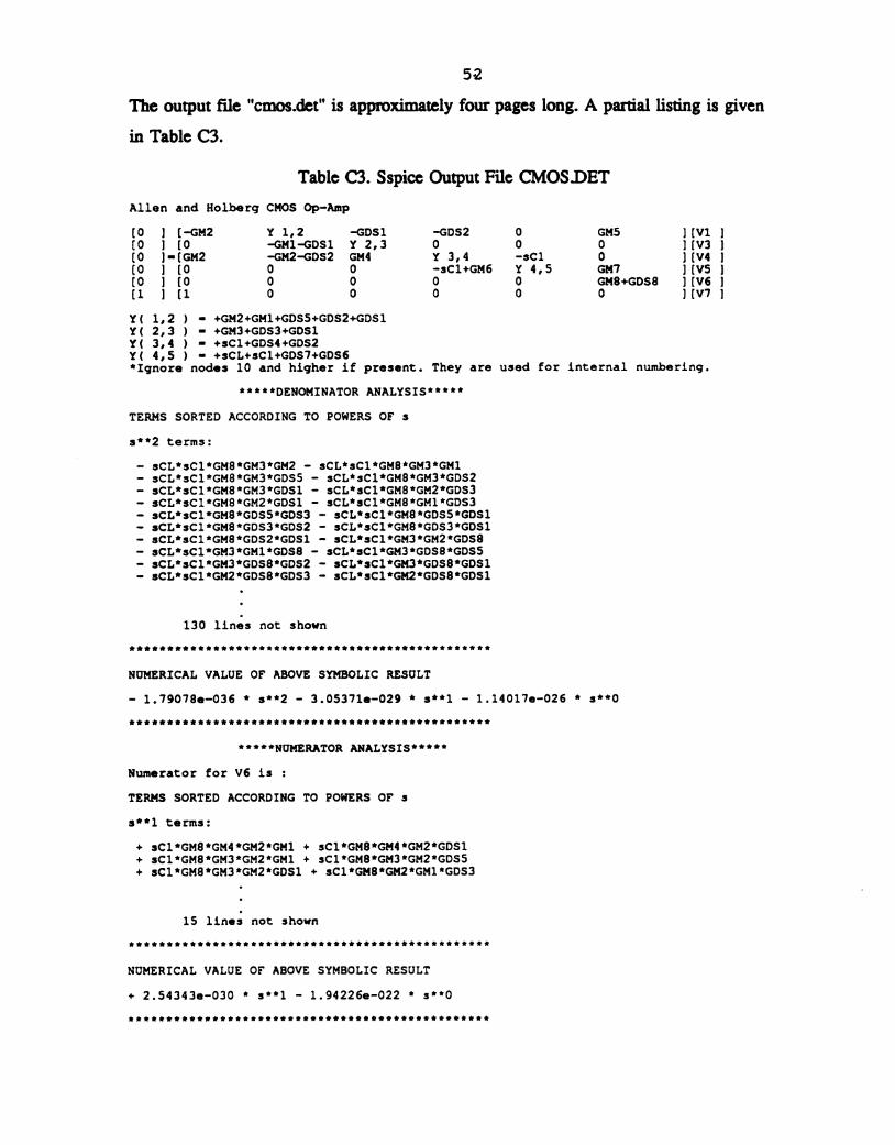
52
The output file "cmos.det" is approximately four pages long. A partial listing is given
in Table C3.
Table C3. Sspice Output File CMOS.DET
Allen and Holberg CMOS Op-Amp
[0 ] [-GM2 Y 1,2 -GDSl -GD52 0 GMS ][Vl ]
[0 l [0 ~GM1-GDSl Y 2,3 0 0 0 ][V3 ]
[0 l-[GMZ -GM2-GD52 GM4 Y 3,4 -sCl 0 ][V4 ]
[O ] [0 0 0 -sC1+GM6 Y 4,5 GM7 ][VS ]
[0 ] [0 0 0 O O GM8+GDSB ][V6 ]
[1 ] [1 0 0 0 0 0 ][V7 ]
Yl 1,2 ) - +GM2+GM1+GDSS+GDSZ+GDSl
Y( 2,3 ) - +GM3+GDS3+GDSI
Y( 3,4 ) - +sC1+GDS4+GDSZ
Y( 4,5 ) - +sCL+sC1+GDS7+GDSS
*Ignore nodes 10 and higher if present. They are used for internal numbering.
*****DENOMINATOR ANALYSIS*****
TERMS SORTED ACCORDING TO POWERS OF S
s**2 terms:
SCL*SC1*GM8*GM3*GM2 - SCL*SC1*GM8'GM3*GM1
SCL'SC1*GM8*GM3*GDSS - sCL*sC1*GM8*GM3*GDSZ
SCL*SC1*GM8*GM3*GD51 - SCL*SC1*GM8*GM2*GD$3
SCL*SC1*GM8*GM2*GDSl - SCL*SC1*GM8*GM1*GDS3
SCL*3C1*GM8*GD55*GDS3 - sCL*sC1*GM8*GDSS*GDSl
8CL*SC1*GM8*GDS3*GDS2 - SCL*SC1*GM8*GDS3*GDSI
SCL*SC1*GM8*GDSZ*GDSI - SCL*SC1'GM3*GM2*GDS8
SCL*SC1*GM3*GM1*GD88 - SCL*SC1*GM3*GDSB*GDS$
SCL*SC1*GM3*GDSB*GDSZ - SCL*SC1*GM3*GDSB*GDSI
SCL*SC1*GM2*GD$8*GDS3 - SCL*SC1*GM2*GD58*GDSI
130 lines not shown
tifititttifitttitttti*ttttttfiiiifitttitttttt*tttttt
NUMERICAL VALUE OF ABOVE SYMBOLIC RESULT
- 1.79078e-036 * s*'2 - 3.05371e-029 * s**l - 1.14017e-026 * s**0
titflittitiittttiiittttflitifitittitiititttttt***ti
*****NUMERATOR ANALYSIS'****
Numerator for V6 is :
TERMS SORTED ACCORDING TO POWERS OF 3
s**1 terms:
+ sC1*GM8*GM4*GM2*GM1 + sC1*GM8*GM4*GM2*GD51
+ SC1*GM8*GM3*GM2*GM1 + sCl'GM8*GM3*GM2*GDSS
+ SCI'GMB'GMB'GM2*GDSI + SCl'GMB'GMZ‘GMl'GDS3
15 lines not shown
titfiiittttflttif!ttittifitittttittittttitti*ttfittt
NUMERICAL VALUE OF ABOVE SYMBOLIC RESULT
+ 2.54343e-030 ' 3*‘1 - 1.94226e-022 * s**0
tfi***t*iitflttitittititititttfiittitittttiiittttit
53
Clearly the full symbolic denominator is so too complicawd to be useful. This symbolic
"explosion" is a central problem in symbolic analysis. Since we know the values of the
transistor parameters (or even just the approximate values), we can simplify the
determinants. The same input file is again run but this time with a magnitude threshold
of 5% or 0.05. The following are the prompts seen by the user. The user responses are
shown in bold:
sepia.
Sspice - Symbolic SPICE Circuit Analyzer
Version 1.0, 1 June 1990
(C) Copyright 1990 by Michigan State University
Unauthorized copying of this program is prohibited
INPUT FILE NAME [.cir] : cmoe
OUTPUT FILENAME [cmos.det] : (bit return)
Would you like the determinant string sorted according to orders of some
variable? (y/n) : n
Would you like a numerical evaluation of the results? (y/n) : y
Do you want the parameter values to be read from the existing .DAT
file? (y/n) : y
Would you like to discard some terms from the answer if their
relative magnitude falls below a certain threshold? (y/n) : y
Please enter the threshold factor (between 0 and 1) : .05
Would you like to see the numerator terms? (y/n) : y
Would you like to prepare a file to check and solve for any second order
filter functions? (y/n) : n
Do you want the numerator terms for V1? (y/n) : n
Do you want the numerator terms for V3? (y/n) : n
Do you want the numerator terms for V4? (y/n) : n
Do you want the numerator terms for V5? (y/n) : n
Do you want the numerator terms for V6? (y/n)
Do you want the numerator terms for V7? (y/n) : n
Note that Sspice looked for the "cmos.dat" file using the same path as that given for
"cmos.cir" and the user was able to avoid having to again supply element values. The user
could also edit this file as appropriate in Other examples. The approximated results found
in "cmos.det" are completely listed in Table C4.
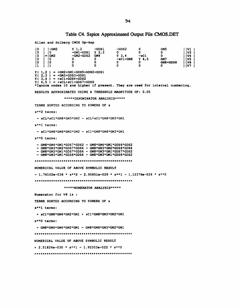
54
Table C4. Sspice Approximated Output File CMOS.DET
Allen and Holberg CMOS Op-Amp
[0 ] {-GMZ Y 1,2 -GDSI -GD52 0 GMS ][VI
[0 l [0 -GMl-GDSl Y 2,3 0 0 0 ][V3
[0 l-[GM2 -GM2-GDSZ GM4 Y 3,4 -sCl 0 ][V4
[0 l [0 0 0 -sCl+GM6 Y 4,5 GM? ][VS
[0 l [O 0 0 0 0 GM8+GD58 ][V6
[1 ] [1 0 0 0 0 0 ][V7
Y( 1,2 ) - +GM2+GM1+GDSS+GDSZ+GDSl
Y( 2,3 ) - +GM3+GDS3+GDSl
Y( 3,4 ) - +sC1+GDs4+GDSZ
Y ) - +sCL+sCl+GDS7+GDS6
*Ignore nodes 10 and higher if present. They are used for internal numbering.
RESULTS APPROXIMATED USING A THRESHOLD MAGNITUDE OF: 0.05
*****DENOMINATOR ANALYSIS*****
TERMS SORTED ACCORDING TO POWERS OF s
s**2 terms:
- sCL*sC1*GM8*GM3*GM2 - sCL*sC1*GM8*GM3*GMl
s**1 terms:
- sCl‘GM8*GM6*GM3*GM2 - sCl‘GM8*GM6*GM3*GM1
s**0 terms:
GM8*GM4*GM1*GDS7*GD52 - GM8‘GM4*GM1*GDSG*GDSZ
GM8*GM3*GM2*GDS7*GDS4 - GM8*GM3*GM2*GDS6*GDS4
GM8*GM3*GM1*GDS7*GDS4 - GM8*GM3*GM1*GDS7*GDSZ
GM8*GM3*GM1*GDSG*GDS4 - GM8*GM3*GM1*GDS€*GDSZ
tt******t***ttitii*ttfiititt*fiititiiittiiitfliitfit
NUMERICAL VALUE OF ABOVE SYMBOLIC RESULT
- 1.76102e-036 * s**2 - 2.95851e-029 * s**1 - 1.12376e-026 * s*'0
ttititfitmittttttttiitittttttitttttittititfitttttt
*****NUMERATOR ANALYSIS*****
Numerator for V6 is :
TERMS SORTED ACCORDING TO POWERS OF s
s'*1 terms:
+ sCl'GMB'GM4'GM2'GM1 + sCl'GM8*GM3*GM2*GM1
s**0 terms:
- GM8‘GM6'GM4‘GM2'GM1 - GM8'GM6'GM3‘GM2*GM1
itttttttttittittttttittttittttttttttitttttittttt
NUMERICAL VALUE OF ABOVE SYMBOLIC RESULT
+ 2.51826e-O30 * s'*1 - 1.92303e-022 * s**0
tfltfififififliififlittfltifittttfliiitttttiitfltfifittiWittit
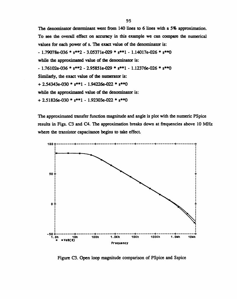
55
The denominator determinant went from 140 lines to 6 lines with a 5% approximation.
To see the overall effect on accuracy in this example we can compare the numerical
values for each power of s. The exact value of the denominator is:
- 1.79078e-036 * s**2 - 3.05371e—029 * s**1 - 1.14017e-026 * s**0
while the approximated value of the denominator is:
- 1.76102e-036 * s**2 - 2.95851e-029 * s**l - 1.12376e-026 * s**0
Similarly, the exact value of the numerator is:
+ 2.54343e-030 * s**l - 1.94226e-022 "' s**0
while the approximated value of the denominator is:
+ 2.51826e-030 * s**1 - 1.92303e-022 * s**0
The approximated transfer function magnitude and angle is plot with the numeric PSpice
results in Figs. C3 and C4. The approximation breaks down at frequencies above 10 MHz
where the transistor capacitance begins to take effect.
_L _.I__. ._.L_
'1'- fi' ‘8" 1" i 1§ '1)-
4)-
I I
I I
I I
I I
I
I I
I I
I I
I I
I I
I I
I I
I I
I I
I I
I I
+ +I I
I I
I I
I I
I I
I I
I I
I I
I I
I I
I I
I I
I I
I I
I I
+ 4-I I
I I
I I
I I
I I
I I
I I
I I
I I
I
I
I
I I
I I
' II
-so+ —+ -I- -I- -I-
1.0): 1% 10M 1.0KI'I 10Kh 100th 1.0Nh 1am
I: uvaaca)
Frequency
Figure C3. Open loop magnitude comparison of PSpice and Sspice
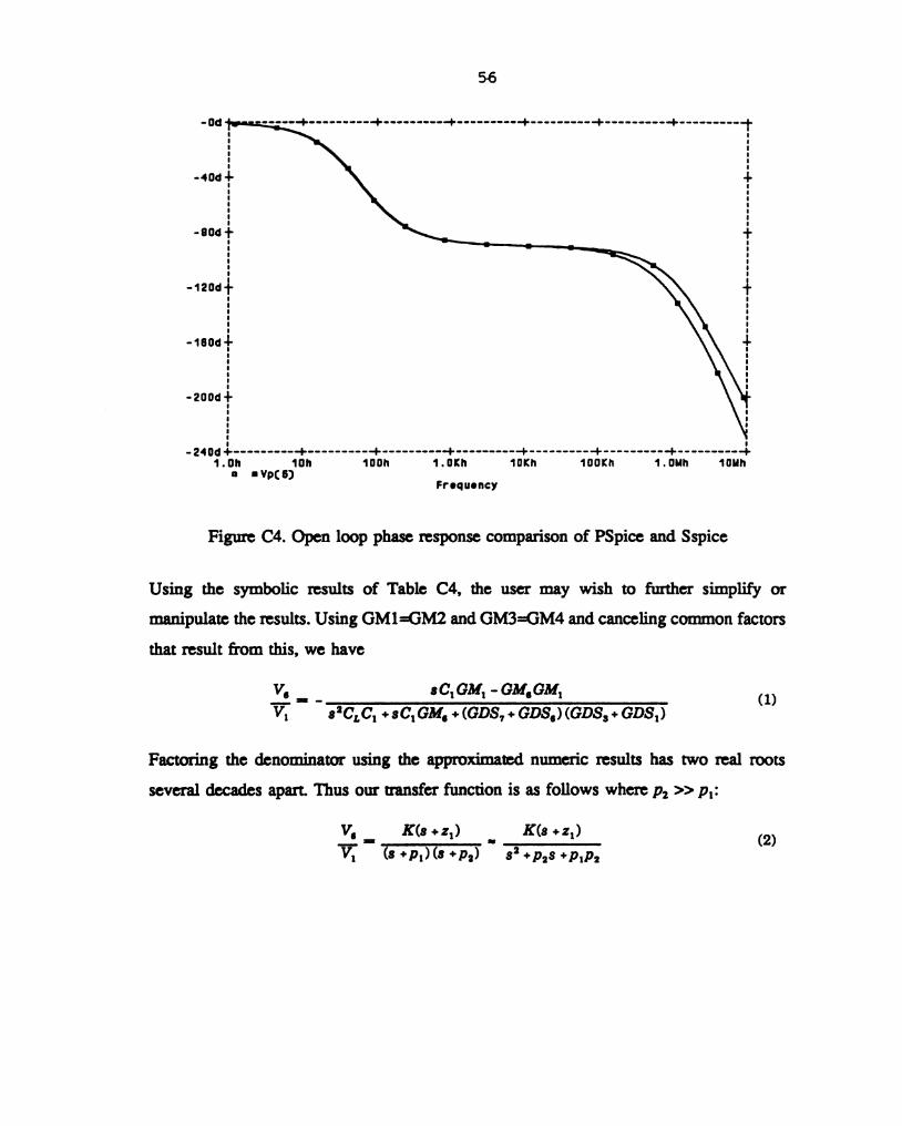
Sfi
I I I
I I I-Ud‘fi: ‘T * ‘r‘
*—------
-4oa'
-80<l ()-
-1znd1r
-130d4)
----+—----I----+----+----4I
-200d4+
-240d-'P----------I-----------I-----------I- ---------—I- --------- -I- --------- -I- ----------+
1.0a 10h roan 1.0Kh 10Kh 100th 1.0un 10Nh
n "9(5)
Frequency
Figure C4. Open loop phase response comparison of PSpice and Sspice
Using the symbolic results of Table C4, the user may wish to further simplify or
manipulate the results. Using GM1=GM2 and GM3=GM4 and canceling common factors
that result from this, we have
v, sqcu, -GM,GM,__ .. .. (1)V. saga, + 30,GM. + (GDS, + GDS.) (GDS, + 0123,)
Factoring the denominator using the approximated numeric results has two real roots
several decades apart. Thus our transfer function is as follows where p2 >> [2,:
V, K(s+z,) n K(s+z,)_ ..(2)
V1 (s +p,) (3 +pg) 8’ +1028 +9192
57
Solving for the room using the approximation in Eqn. 2, we find
GM“ - -2u 12.15MHzz,- -_E_
l
_ GM,
1.
p, - 21: 2.67 MHz
.. (ans, . ans.) (GDS, . 008,)
p‘ c, GM.
— 1 = 21: 60.46 Hz
‘Z‘T—TIW—‘E'I—T.Maw . ,mw . RD 0
The low frequency gain can be found by running the input file with lines containing Cl
and CL removed or taking the limit as s approaches zero in the uansfer function of Eqn.
1. Doing this we find,
v GM,GM,_: - =- 17,065. 84.6dB (3)V,"" WI),. ,)( D ,+GBS',') g
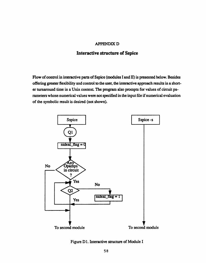
APPENDIX D
Interactive structure of Sspice
Flow ofcontrol in interactive parts ofSspice (modules I and II) is presented below. Besides
offering greater flexibility and control to the user, the interactive approach results in a short-
er turnaround time in a Unix context. The program also prompts for values of circuit pa-
rameters whose numerical values were not specified in the input file ifnumerical evaluation
of the symbolic result is desired (not shown).
Sspice Sspice -s
No
To second module To second module
Figure D1. Interactive structure of Module I
58
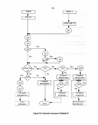
59
sprce -s
Q4
Q5
Yes
Q6
Q7
No Yes
Q8 Q9
Yes Yes Yes
nideal_flag Q11 Q14 Q15
=0?
No
No No
Yes No mpute ompute
Q1 denominator denominator
ompute
Q12 denominator
Q13
ompute ompute ompute
denominator numerator numerator
rror I ter uncnon
estimation END . dentification
Figure D2. Interactive structure of Module II

60
D1.1KEY TO INTERACTIVE PROMPTS
Q1: INPUT FILE NAME [.cir]:
Q2: Is XOAxxx an ideal opamp? (y/n):
Q3: INPUT FILE NAME [.mtx]:
Q4: OUTPUT FILE NAME [xxx.det]:
Q5: Would you like the determinant string sorted according to orders of some variable?
(y/n):
Q6: Would you like numerical evaluation of the results? (y/n):
Q7: Do you want the parameter values to be read from the existing .DAT file? (y/n):
OR (in the event that the .DAT file does not exist)
Do you want to save the parameter values for future invocations of the program? (y/n):
Q8: Would you like to discard some terms from the answer if their relative magnitude falls
below a certain threshold? (y/n):
Q9: Please enter the threshold factor (between 0 and 1):
Q10: Would you like to prepare a file to solve for second order pole shifting due to finite
gain-bandwidth-product (GBP in Hz)? (y/n):
Q11: Would you like to see the numerator terms? (y/n):
Q12: ERROR ANALYSIS FILE NAME [xxx.err]:
Q13: Do you want the GBP’s equated in the ERROR ANALYSIS FILE? (y/n):
Q14: Would you like to prepare a file to check and solve for any second order filter func-
tions? (y/n):
Q15: FILTER FUNCTION FILE NAME [xxx.fun]:
Q16: Do you want the numerator terms for Vxx? (y/n):

BIBLIOGRAPHY
BIBLIOGRAPHY
1. G.Wilson, Y.Bedri and P.Bowron, "RC-Active networks with reduced sensitivity
to amplifier gain-bandwith-preduct," IEEE Trans. on Circuits and Systems, GAS-21,
pp. 618-626, September 1974.
2. LA. Svoboda, G.M. Wierzba and T.Reynolds, " Op-amp relocation, the complemen-
tary and stability," Proc. 29th Midwest Symposium on Circuits and Systems, August,
1986.
3. G.M. Wierzba and LA. Svoboda, "An op-amp relocated bandpass filter with zero
center frequency sensitivity to the gain-bandwith-product," Proc. 29th Midwest Sym-
posium on Circuits and Systems, pp. 28-32, August, 1986.
4. G.M. Wierzba and J.A.Svoboda, "A comparison of circuits generated by op-amp
relocation," Proc. 23rd Midwest Symposium on Circuits and Systems, pp. 800-804, Au-
gust 1980.
5. L.T.Bruton, RC-Active Circuits Theory and Design, Prentice Hall, 1980.
6. GM. Wierzba, "Op-amp relocation: A topological active network synthesis," IEEE
Trans. on Circuits and Systems, GAS-33, pp469-475, May 1986.
7. G.M.Wierzba, A.Srivastava, VJoshi, K.V.Noren and I.A.Svoboda, "Sspice: A sym-
bolic SPICE program for linear active circuits," Invited, 32nd Midwest Symposium
on Circuits and Systems, pp 1197-1201,May 1989.
8. A.Srivastava and G.M. Wierzba,"Symbolic approximation of analog circuits using
Sspice", Invited, 33rd Midwest Symposium on Circuits and Systems, August 1990.
61

6 2
9. P. Sannuti and N.N. Pmi, "Symbolic network analysis-An algebraic formulation," IEEE
Trans. on Circuits and Systems, GAS-27, pp 679-687, August 1980.
10. V. Joshi. "SLAP : Symbolic Linear Analysis Program," MS thesis, Michigan State Uni-
versity, E. Lansing MI, 1987.

HIGRN STRTE UNIV.
1113111113111111311111111 311113111111311311111111131115