Embed Size (px)
Citation preview
RT3602AC®
DS3602AC-01 June 2017 www.richtek.com1
©Copyright 2017 Richtek Technology Corporation. All rights reserved. is a registered trademark of Richtek Technology Corporation.
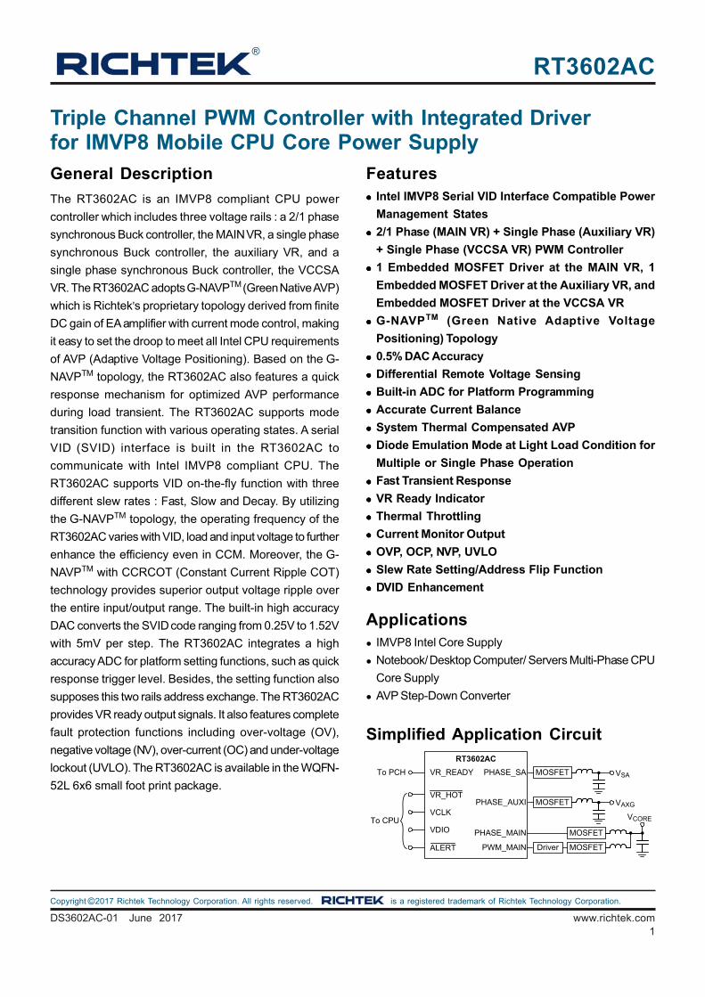
Simplified Application Circuit
Triple Channel PWM Controller with Integrated Driverfor IMVP8 Mobile CPU Core Power SupplyGeneral Description
The RT3602AC is an IMVP8 compliant CPU power
controller which includes three voltage rails : a 2/1 phase
synchronous Buck controller, the MAIN VR, a single phase
synchronous Buck controller, the auxiliary VR, and a
single phase synchronous Buck controller, the VCCSA
VR. The RT3602AC adopts G-NAVPTM (Green Native AVP)
which is Richtek's proprietary topology derived from finite
DC gain of EA amplifier with current mode control, making
it easy to set the droop to meet all Intel CPU requirements
of AVP (Adaptive Voltage Positioning). Based on the G-
NAVPTM topology, the RT3602AC also features a quick
response mechanism for optimized AVP performance
during load transient. The RT3602AC supports mode
transition function with various operating states. A serial
VID (SVID) interface is built in the RT3602AC to
communicate with Intel IMVP8 compliant CPU. The
RT3602AC supports VID on-the-fly function with three
different slew rates : Fast, Slow and Decay. By utilizing
the G-NAVPTM topology, the operating frequency of the
RT3602AC varies with VID, load and input voltage to further
enhance the efficiency even in CCM. Moreover, the G-
NAVPTM with CCRCOT (Constant Current Ripple COT)
technology provides superior output voltage ripple over
the entire input/output range. The built-in high accuracy
DAC converts the SVID code ranging from 0.25V to 1.52V
with 5mV per step. The RT3602AC integrates a high
accuracy ADC for platform setting functions, such as quick
response trigger level. Besides, the setting function also
supposes this two rails address exchange. The RT3602AC
provides VR ready output signals. It also features complete
fault protection functions including over-voltage (OV),
negative voltage (NV), over-current (OC) and under-voltage
lockout (UVLO). The RT3602AC is available in the WQFN-
52L 6x6 small foot print package.
Features Intel IMVP8 Serial VID Interface Compatible Power
Management States
2/1 Phase (MAIN VR) + Single Phase (Auxiliary VR)
+ Single Phase (VCCSA VR) PWM Controller
1 Embedded MOSFET Driver at the MAIN VR, 1
Embedded MOSFET Driver at the Auxiliary VR, and
Embedded MOSFET Driver at the VCCSA VR
G-NAVPTM (Green Native Adaptive Voltage
Positioning) Topology
0.5% DAC Accuracy
Differential Remote Voltage Sensing
Built-in ADC for Platform Programming
Accurate Current Balance
System Thermal Compensated AVP
Diode Emulation Mode at Light Load Condition for
Multiple or Single Phase Operation
Fast Transient Response
VR Ready Indicator
Thermal Throttling
Current Monitor Output
OVP, OCP, NVP, UVLO
Slew Rate Setting/Address Flip Function
DVID Enhancement
Applications IMVP8 Intel Core Supply
Notebook/ Desktop Computer/ Servers Multi-Phase CPU
Core Supply
AVP Step-Down Converter
RT3602AC
PHASE_MAIN
PWM_MAIN Driver
VSAPHASE_SA MOSFETVR_READY
VCLK
VDIO
VR_HOT
ALERT
VCORE
PHASE_AUXI MOSFET
To PCH
To CPU
VAXG
MOSFET
MOSFET
2
RT3602AC
www.richtek.com DS3602AC-01 June 2017
©Copyright 2017 Richtek Technology Corporation. All rights reserved. is a registered trademark of Richtek Technology Corporation.
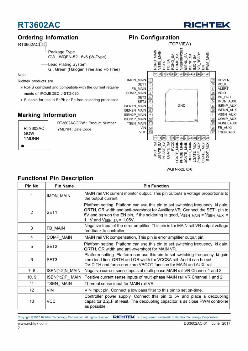
Functional Pin DescriptionPin No Pin Name Pin Function
1 IMON_MAIN MAIN rail VR current monitor output. This pin outputs a voltage proportional to the output current.
2 SET1
Platform setting. Platform can use this pin to set switching frequency, ki gain, QRTH, QR width and anti-overshoot for Auxiliary VR. Connect the SET1 pin to 5V and turn-on the EN pin, if the soldering is good, VSEN_MAIN = VSEN_AUXI = 1.1V and VSEN_SA = 1.05V.
3 FB_MAIN Negative Input of the error amplifier. This pin is for MAIN rail VR output voltage feedback to controller.
4 COMP_MAIN MAIN rail VR compensation. This pin is error amplifier output pin.
5 SET2 Platform setting. Platform can use this pin to set switching frequency, ki gain, QRTH, QR width and anti-overshoot for MAIN VR.
6 SET3 Platform setting. Platform can use this pin to set switching frequency, ki gain zero load-line, QRTH and QR width for VCCSA rail. And it can be set DVID TH and force-non-zero VBOOT function for MAIN and AUXI rail.
7, 8 ISEN[1:2]N_MAIN Negative current sense inputs of multi-phase MAIN rail VR Channel 1 and 2.
10, 9 ISEN[1:2]P_ MAIN Positive current sense inputs of multi-phase MAIN rail VR Channel 1 and 2.
11 TSEN_ MAIN Thermal sense input for MAIN rail VR.
12 VIN VIN input pin. Connect a low pass filter to this pin to set on-time.
13 VCC Controller power supply. Connect this pin to 5V and place a decoupling capacitor 2.2F at least. The decoupling capacitor is as close PWM controller as possible.
Ordering Information
Note :
Richtek products are :
RoHS compliant and compatible with the current require-
ments of IPC/JEDEC J-STD-020.
Suitable for use in SnPb or Pb-free soldering processes.
Pin Configuration(TOP VIEW)
WQFN-52L 6x6
Marking InformationRT3602ACGQW : Product Number
YMDNN : Date CodeRT3602ACGQWYMDNN
Package TypeQW : WQFN-52L 6x6 (W-Type)
RT3602AC
Lead Plating SystemG : Green (Halogen Free and Pb Free) V
SE
N_
MA
INP
SY
SF
B_
SA
RG
ND
_SA
CO
MP
_S
A
EN
VR
EF
06/P
SE
TIS
EN
N_S
AIS
EN
P_
SA
IMO
N_
SA
PW
M_M
AIN
RG
ND
_MA
IN
VR
_R
EA
DY
IMON_MAIN
COMP_MAINFB_MAIN
VINTSEN_MAIN
ISEN1P_MAINISEN2P_MAINISEN2N_MAINISEN1N_MAIN
SET2SET3
SET1
BO
OT
_S
AU
GA
TE
_S
AP
HA
SE
_S
ALG
AT
E_
SA
PV
CC
UG
AT
E_
AU
XI
PH
AS
E_M
AIN
UG
AT
E_M
AIN
BO
OT
_MA
INLG
AT
E_
AU
XI
PH
AS
E_
AU
XI
DRVEN
VDIOALERT
RGND_AUXICOMP_AUXIVSEN_AUXIISENN_AUXIISENP_AUXI
VR_HOTIMON_AUXI
VCLK1
2
3
4
5
6
7
8
9
10
11
12
252423222120191817161514
39
38
37
36
35
34
33
32
31
30
29
414243444546474849505152
FB_AUXI28
TSEN_AUXI27
BO
OT
_A
UX
I
26
VCC 13
40
GND
53
LGA
TE
_MA
IN
3
RT3602AC
DS3602AC-01 June 2017 www.richtek.com
©Copyright 2017 Richtek Technology Corporation. All rights reserved. is a registered trademark of Richtek Technology Corporation.
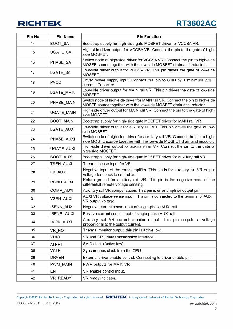
Pin No Pin Name Pin Function
14 BOOT_SA Bootstrap supply for high-side gate MOSFET driver for VCCSA VR.
15 UGATE_SA High-side driver output for VCCSA VR. Connect the pin to the gate of high-side MOSFET.
16 PHASE_SA Switch node of high-side driver for VCCSA VR. Connect the pin to high-side MOSFE source together with the low-side MOSFET drain and inductor.
17 LGATE_SA Low-side driver output for VCCSA VR. This pin drives the gate of low-side MOSFET.
18 PVCC Driver power supply input. Connect this pin to GND by a minimum 2.2μF ceramic Capacitor.
19 LGATE_MAIN Low-side driver output for MAIN rail VR. This pin drives the gate of low-side MOSFET.
20 PHASE_MAIN Switch node of high-side driver for MAIN rail VR. Connect the pin to high-side MOSFE source together with the low-side MOSFET drain and inductor.
21 UGATE_MAIN High-side driver output for MAIN rail VR. Connect the pin to the gate of high-side MOSFET.
22 BOOT_MAIN Bootstrap supply for high-side gate MOSFET driver for MAIN rail VR.
23 LGATE_AUXI Low-side driver output for auxiliary rail VR. This pin drives the gate of low-side MOSFET.
24 PHASE_AUXI Switch node of high-side driver for auxiliary rail VR. Connect the pin to high-side MOSFE source together with the low-side MOSFET drain and inductor.
25 UGATE_AUXI High-side driver output for auxiliary rail VR. Connect the pin to the gate of high-side MOSFET.
26 BOOT_AUXI Bootstrap supply for high-side gate MOSFET driver for auxiliary rail VR.
27 TSEN_AUXI Thermal sense input for VR.
28 FB_AUXI Negative input of the error amplifier. This pin is for auxiliary rail VR output voltage feedback to controller.
29 RGND_AUXI Return ground for auxiliary rail VR. This pin is the negative node of the differential remote voltage sensing.
30 COMP_AUXI Auxiliary rail VR compensation. This pin is error amplifier output pin.
31 VSEN_AUXI AUXI VR voltage sense input. This pin is connected to the terminal of AUXI VR output voltage.
32 ISENN_AUXI Negative current sense input of single-phase AUXI rail.
33 ISENP_ AUXI Positive current sense input of single-phase AUXI rail.
34 IMON_AUXI Auxiliary rail VR current monitor output. This pin outputs a voltage proportional to the output current.
35 VR_HOT Thermal monitor output, this pin is active low.
36 VDIO VR and CPU data transmission interface.
37 ALERT SVID alert. (Active low)
38 VCLK Synchronous clock from the CPU.
39 DRVEN External driver enable control. Connecting to driver enable pin.
40 PWM_MAIN PWM outputs for MAIN VR.
41 EN VR enable control input.
42 VR_READY VR ready indicator.
4
RT3602AC
www.richtek.com DS3602AC-01 June 2017
©Copyright 2017 Richtek Technology Corporation. All rights reserved. is a registered trademark of Richtek Technology Corporation.
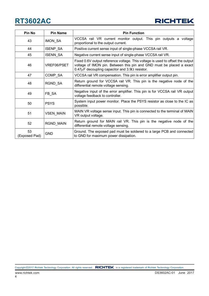
Pin No Pin Name Pin Function
43 IMON_SA VCCSA rail VR current monitor output. This pin outputs a voltage proportional to the output current.
44 ISENP_SA Positive current sense input of single-phase VCCSA rail VR.
45 ISENN_SA Negative current sense input of single-phase VCCSA rail VR.
46 VREF06/PSET Fixed 0.6V output reference voltage. This voltage is used to offset the output voltage of IMON pin. Between this pin and GND must be placed a exact 0.47F decoupling capacitor and 3.9 resistor.
47 COMP_SA VCCSA rail VR compensation. This pin is error amplifier output pin.
48 RGND_SA Return ground for VCCSA rail VR. This pin is the negative node of the differential remote voltage sensing.
49 FB_SA Negative input of the error amplifier. This pin is for VCCSA rail VR output voltage feedback to controller.
50 PSYS System input power monitor. Place the PSYS resistor as close to the IC as possible.
51 VSEN_MAIN MAIN VR voltage sense input. This pin is connected to the terminal of MAIN VR output voltage.
52 RGND_MAIN Return ground for MAIN rail VR. This pin is the negative node of the differential remote voltage sensing.
53 (Exposed Pad)
GND Ground. The exposed pad must be soldered to a large PCB and connected to GND for maximum power dissipation.
5
RT3602AC
DS3602AC-01 June 2017 www.richtek.com
©Copyright 2017 Richtek Technology Corporation. All rights reserved. is a registered trademark of Richtek Technology Corporation.
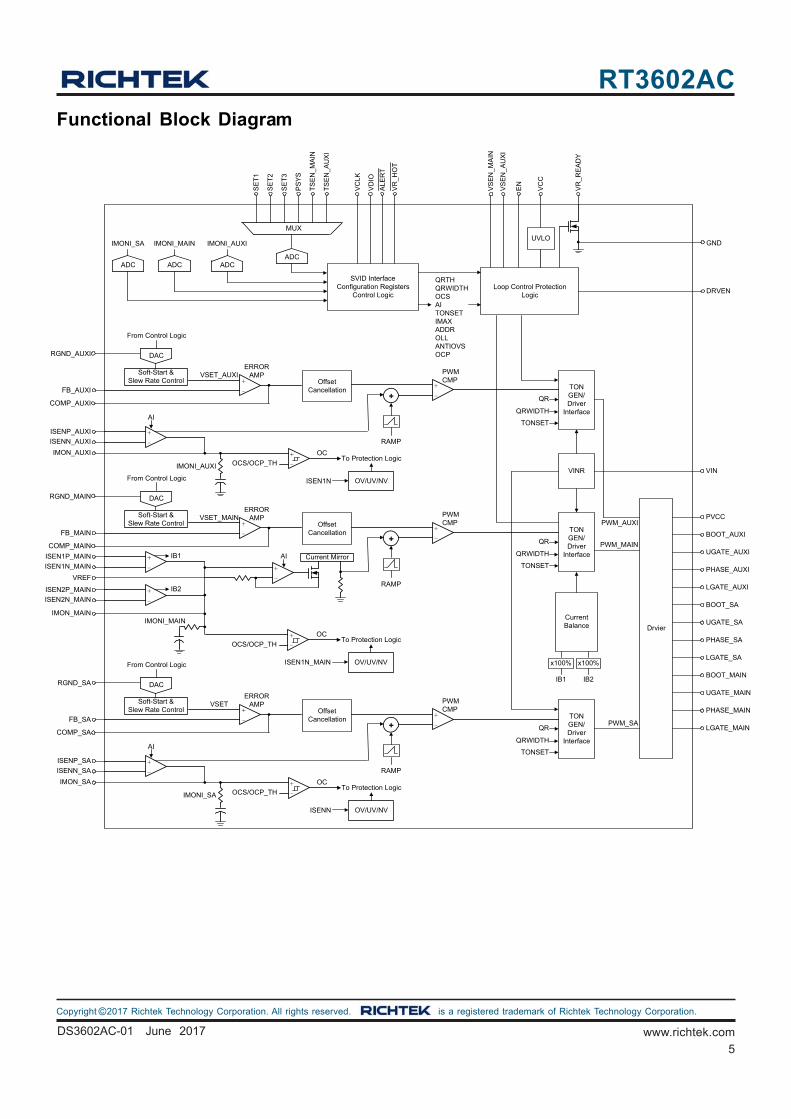
Functional Block Diagram
Loop Control Protection Logic
SVID InterfaceConfiguration Registers
Control Logic
UVLO
FB_AUXI
COMP_AUXI
RGND_AUXI
Soft-Start & Slew Rate Control
VSET_AUXIERROR
AMP
From Control Logic
Offset Cancellation
ISENN_AUXI
ISENP_AUXI
+
-
+
-
DAC
TON GEN/ Driver
Interface
+
-
PWMCMP
+
-
+
RAMP
OV/UV/NV
OCS/OCP_TH
QRWIDTH
TONSET
QR
PWM_AUXI
VC
C
VD
IO
VC
LK
VR
_RE
AD
Y
SE
T1
QRTHQRWIDTHOCSAITONSETIMAXADDROLLANTIOVSOCP
EN
ADC
MUX
VR
_HO
T
ALE
RT
ADC ADC ADCS
ET
2
SE
T3
VS
EN
_M
AIN
VS
EN
_A
UX
I
PS
YS
TS
EN
_MA
IN
TS
EN
_AU
XI
IMONI_AUXIIMONI_MAINIMONI_SA
To Protection LogicOC
AI
IMON_AUXI
ISEN1N
FB_MAIN
COMP_MAIN
RGND_MAIN
Soft-Start & Slew Rate Control
VSET_MAINERROR
AMP
From Control Logic
Offset Cancellation
ISEN1N_MAIN
ISEN1P_MAIN
+
-
+
-
DAC
TON GEN/ Driver
Interface+
-
PWMCMP
+
RAMP
QRWIDTH
TONSET
QR
IB1
VREF
+
-
Current MirrorAI
ISEN2N_MAIN
ISEN2P_MAIN +
-
IB2
IMON_MAIN
+
-
OV/UV/NV
OCS/OCP_THTo Protection Logic
OC
ISEN1N_MAIN
IMONI_MAIN
FB_SA
COMP_SA
RGND_SA
Soft-Start & Slew Rate Control
VSET ERROR
AMP
From Control Logic
Offset Cancellation
ISENN_SA
ISENP_SA
+
-
+
-
DAC
TON GEN/ Driver
Interface
+
-
PWMCMP
+
-
+
RAMP
OV/UV/NV
OCS/OCP_TH
QRWIDTH
TONSET
QRPWM_SA
To Protection LogicOC
AI
IMON_SA
ISENN
IMONI_AUXI
IMONI_SA
VINR
PWM_MAIN
Current Balance
IB2
x100%
IB1
x100%
GND
DRVEN
VIN
Drvier
PVCC
BOOT_AUXI
UGATE_AUXI
PHASE_AUXI
LGATE_AUXI
BOOT_SA
UGATE_SA
PHASE_SA
LGATE_SA
BOOT_MAIN
UGATE_MAIN
PHASE_MAIN
LGATE_MAIN
6
RT3602AC
www.richtek.com DS3602AC-01 June 2017
©Copyright 2017 Richtek Technology Corporation. All rights reserved. is a registered trademark of Richtek Technology Corporation.
Operation
The RT3602AC adopts G-NAVPTM (Green Native AVP)
which is Richtek's proprietary topology derived from finite
DC gain of EA amplifier with current mode control, making
it easy to set the droop to meet all Intel CPU requirements
of AVP (Adaptive Voltage Positioning).
The G-NAVPTM controller is one type of current mode
constant on-time control with DC offset cancellation. The
approach can not only improve DC offset problem for
increasing system accuracy but also provide fast transient
response. When current feedback signal reaches COMP
signal, the RT3602AC generates an on-time width to
achieve PWM modulation.
TON GEN/Driver Interface PWMx
Generate the sequentially according to the phase control
signal from the Loop Control/Protection Logic. Pulse width
is determined by current balance result and pin setting.
Once quick response mechanism is triggered, VR will
allow all PWM to turn on at the same time. PWM status
is also controlled by Protection Logic. Different protections
may cause different PWM status (Both High-Z or LG turn-
on).
SVID Interface/Configuration Registers/Control
Logic
The interface receives the SVID signal from CPU and sends
the relative signals to Loop Control/Protection Logic for
loop control to execute the action by CPU. The registers
save the pin setting data from ADC output. The Control
Logic controls the ADC timing, generates the digital code
of the VID for VSEN voltage.
Loop Control/Protection Logic
It controls the power on sequence, the protection behavior,
and the operational phase number.
MUX and ADC
The MUX supports the inputs from SET1, SET2, SET3,
IMON_MAIN, IMON_AUXI, TSEN_MAIN and TSEN_AUXI.
The ADC converts these analog signals to digital codes
for reporting or performance adjustment.
Current Balance
Each phase current sense signal is sent to the current
balance circuit which adjusts the on-time of each phase
to optimize current sharing.
Offset Cancellation
Cancel the current/voltage ripple issue to get the accurate
VSEN.
UVLO
Detect the VCC voltage and issue POR signal as they
are high enough.
DAC
Generate an analog signal according to the digital code
generated by Control Logic.
Soft-Start & Slew Rate Control
Control the Dynamic VID slew rate of VSEN according to
the SetVID fast or SetVID slow.
Error Amp
Error amplifier generates COMP_MAIN/COMP_AUXI/
COMP_SA signal by the difference between output of
MAIN/Auxiliary/SA rail and FB_MAIN/FB_AUXI/FB_SA.
PWM CMP
The PWM comparator compares COMP signal and current
feedback signal to generate a signal for TON trigger.
IMON Filter
IMON Filter is used for average sum current signal by
analog RC filter.
7
RT3602AC
DS3602AC-01 June 2017 www.richtek.com
©Copyright 2017 Richtek Technology Corporation. All rights reserved. is a registered trademark of Richtek Technology Corporation.
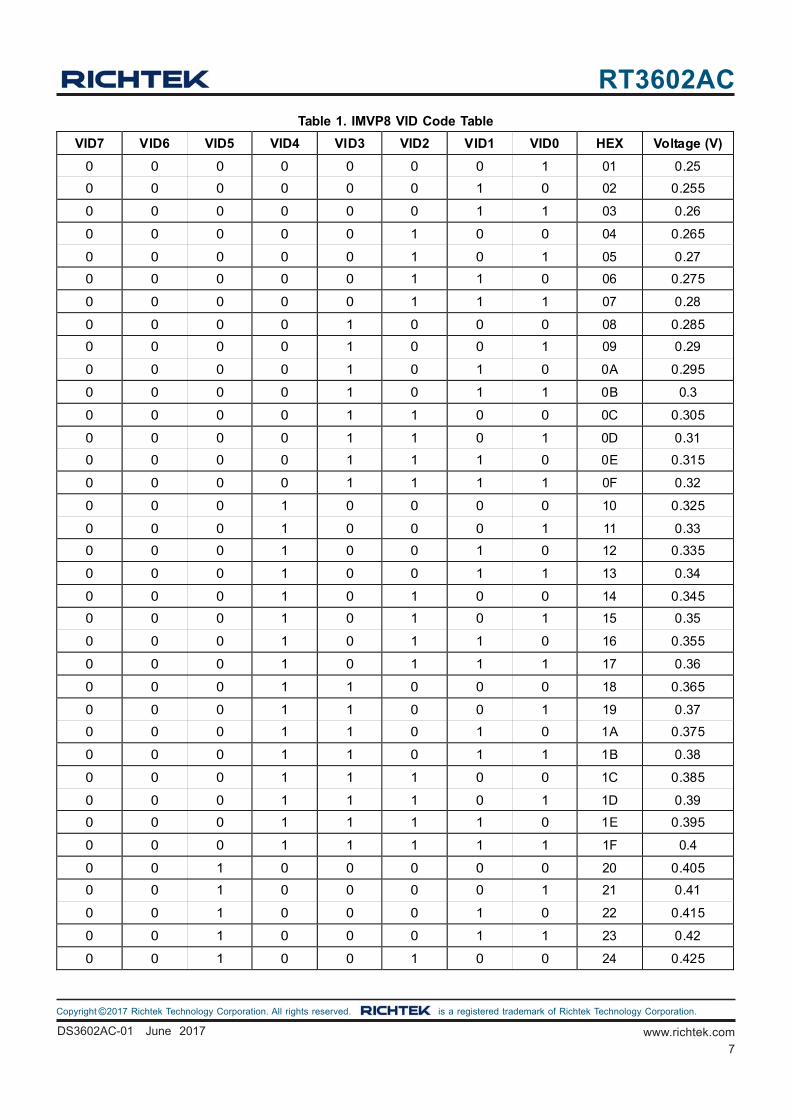
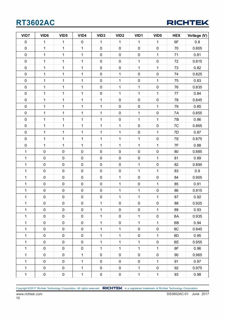
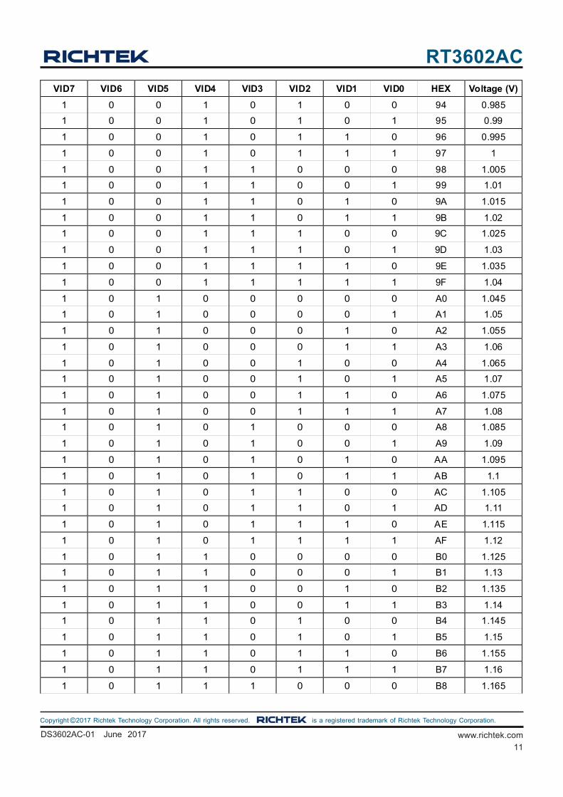
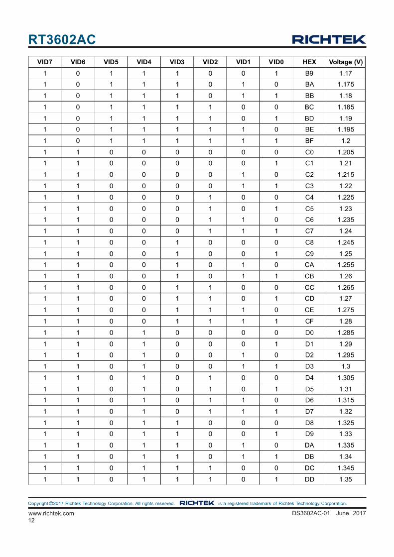
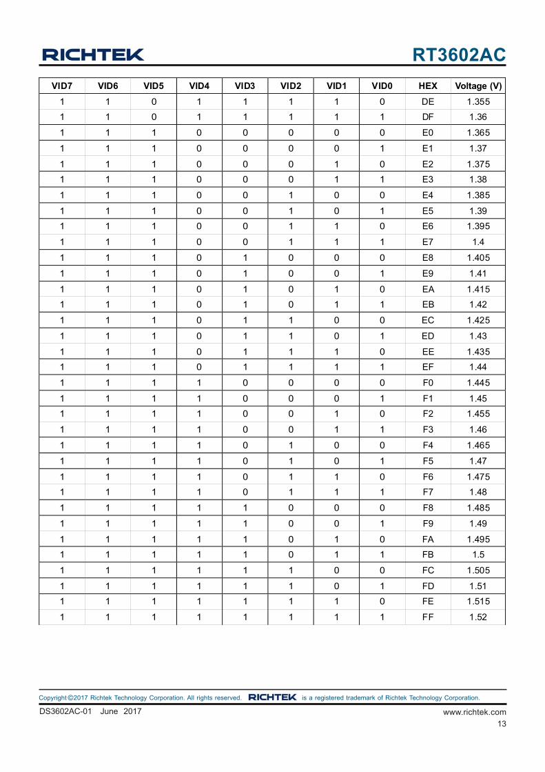
Table 1. IMVP8 VID Code Table
VID7 VID6 VID5 VID4 VID3 VID2 VID1 VID0 HEX Voltage (V)
0 0 0 0 0 0 0 1 01 0.25
0 0 0 0 0 0 1 0 02 0.255
0 0 0 0 0 0 1 1 03 0.26
0 0 0 0 0 1 0 0 04 0.265
0 0 0 0 0 1 0 1 05 0.27
0 0 0 0 0 1 1 0 06 0.275
0 0 0 0 0 1 1 1 07 0.28
0 0 0 0 1 0 0 0 08 0.285
0 0 0 0 1 0 0 1 09 0.29
0 0 0 0 1 0 1 0 0A 0.295
0 0 0 0 1 0 1 1 0B 0.3
0 0 0 0 1 1 0 0 0C 0.305
0 0 0 0 1 1 0 1 0D 0.31
0 0 0 0 1 1 1 0 0E 0.315
0 0 0 0 1 1 1 1 0F 0.32
0 0 0 1 0 0 0 0 10 0.325
0 0 0 1 0 0 0 1 11 0.33
0 0 0 1 0 0 1 0 12 0.335
0 0 0 1 0 0 1 1 13 0.34
0 0 0 1 0 1 0 0 14 0.345
0 0 0 1 0 1 0 1 15 0.35
0 0 0 1 0 1 1 0 16 0.355
0 0 0 1 0 1 1 1 17 0.36
0 0 0 1 1 0 0 0 18 0.365
0 0 0 1 1 0 0 1 19 0.37
0 0 0 1 1 0 1 0 1A 0.375
0 0 0 1 1 0 1 1 1B 0.38
0 0 0 1 1 1 0 0 1C 0.385
0 0 0 1 1 1 0 1 1D 0.39
0 0 0 1 1 1 1 0 1E 0.395
0 0 0 1 1 1 1 1 1F 0.4
0 0 1 0 0 0 0 0 20 0.405
0 0 1 0 0 0 0 1 21 0.41
0 0 1 0 0 0 1 0 22 0.415
0 0 1 0 0 0 1 1 23 0.42
0 0 1 0 0 1 0 0 24 0.425
8
RT3602AC
www.richtek.com DS3602AC-01 June 2017
©Copyright 2017 Richtek Technology Corporation. All rights reserved. is a registered trademark of Richtek Technology Corporation.
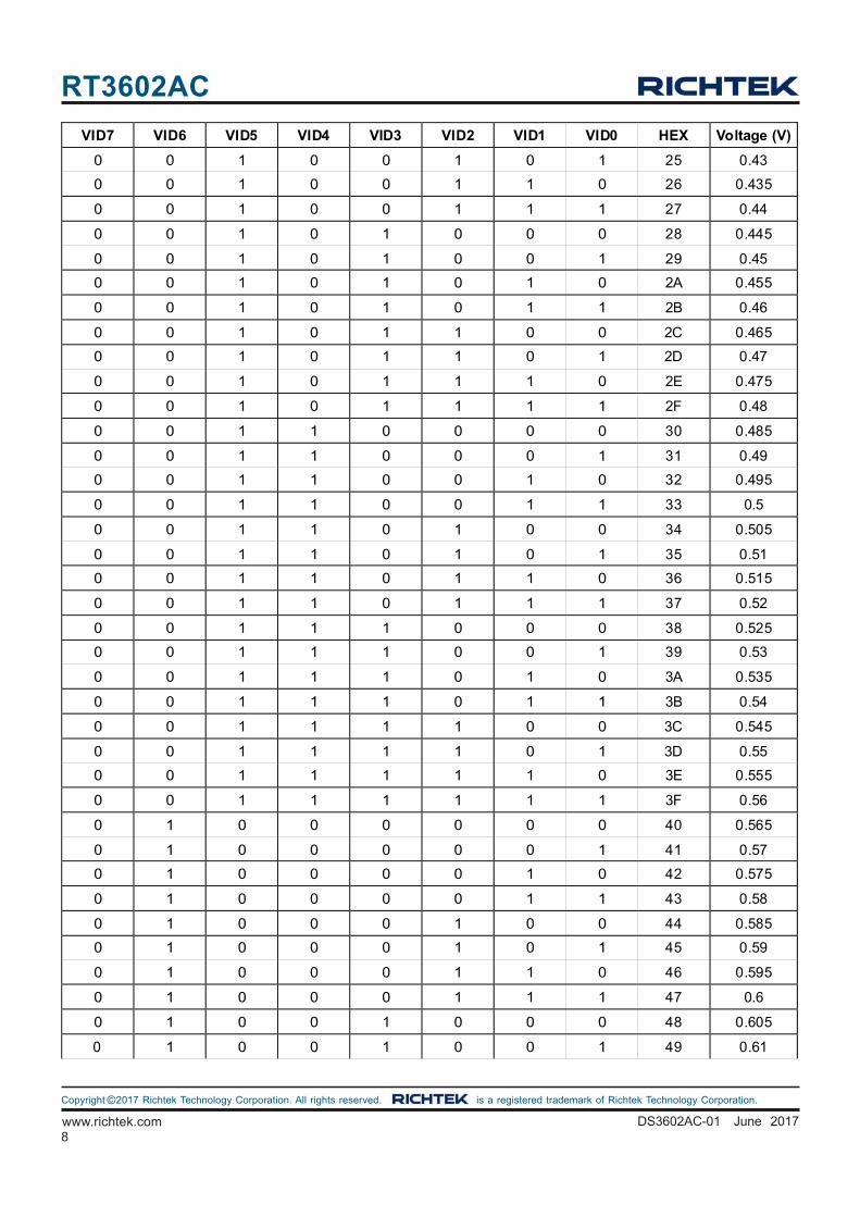
VID7 VID6 VID5 VID4 VID3 VID2 VID1 VID0 HEX Voltage (V)
0 0 1 0 0 1 0 1 25 0.43
0 0 1 0 0 1 1 0 26 0.435
0 0 1 0 0 1 1 1 27 0.44
0 0 1 0 1 0 0 0 28 0.445
0 0 1 0 1 0 0 1 29 0.45
0 0 1 0 1 0 1 0 2A 0.455
0 0 1 0 1 0 1 1 2B 0.46
0 0 1 0 1 1 0 0 2C 0.465
0 0 1 0 1 1 0 1 2D 0.47
0 0 1 0 1 1 1 0 2E 0.475
0 0 1 0 1 1 1 1 2F 0.48
0 0 1 1 0 0 0 0 30 0.485
0 0 1 1 0 0 0 1 31 0.49
0 0 1 1 0 0 1 0 32 0.495
0 0 1 1 0 0 1 1 33 0.5
0 0 1 1 0 1 0 0 34 0.505
0 0 1 1 0 1 0 1 35 0.51
0 0 1 1 0 1 1 0 36 0.515
0 0 1 1 0 1 1 1 37 0.52
0 0 1 1 1 0 0 0 38 0.525
0 0 1 1 1 0 0 1 39 0.53
0 0 1 1 1 0 1 0 3A 0.535
0 0 1 1 1 0 1 1 3B 0.54
0 0 1 1 1 1 0 0 3C 0.545
0 0 1 1 1 1 0 1 3D 0.55
0 0 1 1 1 1 1 0 3E 0.555
0 0 1 1 1 1 1 1 3F 0.56
0 1 0 0 0 0 0 0 40 0.565
0 1 0 0 0 0 0 1 41 0.57
0 1 0 0 0 0 1 0 42 0.575
0 1 0 0 0 0 1 1 43 0.58
0 1 0 0 0 1 0 0 44 0.585
0 1 0 0 0 1 0 1 45 0.59
0 1 0 0 0 1 1 0 46 0.595
0 1 0 0 0 1 1 1 47 0.6
0 1 0 0 1 0 0 0 48 0.605
0 1 0 0 1 0 0 1 49 0.61
9
RT3602AC
DS3602AC-01 June 2017 www.richtek.com
©Copyright 2017 Richtek Technology Corporation. All rights reserved. is a registered trademark of Richtek Technology Corporation.
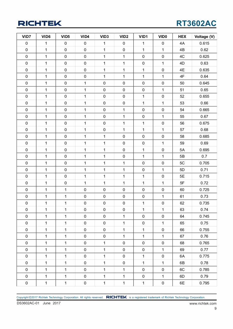
VID7 VID6 VID5 VID4 VID3 VID2 VID1 VID0 HEX Voltage (V)
0 1 0 0 1 0 1 0 4A 0.615
0 1 0 0 1 0 1 1 4B 0.62
0 1 0 0 1 1 0 0 4C 0.625
0 1 0 0 1 1 0 1 4D 0.63
0 1 0 0 1 1 1 0 4E 0.635
0 1 0 0 1 1 1 1 4F 0.64
0 1 0 1 0 0 0 0 50 0.645
0 1 0 1 0 0 0 1 51 0.65
0 1 0 1 0 0 1 0 52 0.655
0 1 0 1 0 0 1 1 53 0.66
0 1 0 1 0 1 0 0 54 0.665
0 1 0 1 0 1 0 1 55 0.67
0 1 0 1 0 1 1 0 56 0.675
0 1 0 1 0 1 1 1 57 0.68
0 1 0 1 1 0 0 0 58 0.685
0 1 0 1 1 0 0 1 59 0.69
0 1 0 1 1 0 1 0 5A 0.695
0 1 0 1 1 0 1 1 5B 0.7
0 1 0 1 1 1 0 0 5C 0.705
0 1 0 1 1 1 0 1 5D 0.71
0 1 0 1 1 1 1 0 5E 0.715
0 1 0 1 1 1 1 1 5F 0.72
0 1 1 0 0 0 0 0 60 0.725
0 1 1 0 0 0 0 1 61 0.73
0 1 1 0 0 0 1 0 62 0.735
0 1 1 0 0 0 1 1 63 0.74
0 1 1 0 0 1 0 0 64 0.745
0 1 1 0 0 1 0 1 65 0.75
0 1 1 0 0 1 1 0 66 0.755
0 1 1 0 0 1 1 1 67 0.76
0 1 1 0 1 0 0 0 68 0.765
0 1 1 0 1 0 0 1 69 0.77
0 1 1 0 1 0 1 0 6A 0.775
0 1 1 0 1 0 1 1 6B 0.78
0 1 1 0 1 1 0 0 6C 0.785
0 1 1 0 1 1 0 1 6D 0.79
0 1 1 0 1 1 1 0 6E 0.795
10
RT3602AC
www.richtek.com DS3602AC-01 June 2017
©Copyright 2017 Richtek Technology Corporation. All rights reserved. is a registered trademark of Richtek Technology Corporation.
VID7 VID6 VID5 VID4 VID3 VID2 VID1 VID0 HEX Voltage (V)
0 1 1 0 1 1 1 1 6F 0.8
0 1 1 1 0 0 0 0 70 0.805
0 1 1 1 0 0 0 1 71 0.81
0 1 1 1 0 0 1 0 72 0.815
0 1 1 1 0 0 1 1 73 0.82
0 1 1 1 0 1 0 0 74 0.825
0 1 1 1 0 1 0 1 75 0.83
0 1 1 1 0 1 1 0 76 0.835
0 1 1 1 0 1 1 1 77 0.84
0 1 1 1 1 0 0 0 78 0.845
0 1 1 1 1 0 0 1 79 0.85
0 1 1 1 1 0 1 0 7A 0.855
0 1 1 1 1 0 1 1 7B 0.86
0 1 1 1 1 1 0 0 7C 0.865
0 1 1 1 1 1 0 1 7D 0.87
0 1 1 1 1 1 1 0 7E 0.875
0 1 1 1 1 1 1 1 7F 0.88
1 0 0 0 0 0 0 0 80 0.885
1 0 0 0 0 0 0 1 81 0.89
1 0 0 0 0 0 1 0 82 0.895
1 0 0 0 0 0 1 1 83 0.9
1 0 0 0 0 1 0 0 84 0.905
1 0 0 0 0 1 0 1 85 0.91
1 0 0 0 0 1 1 0 86 0.915
1 0 0 0 0 1 1 1 87 0.92
1 0 0 0 1 0 0 0 88 0.925
1 0 0 0 1 0 0 1 89 0.93
1 0 0 0 1 0 1 0 8A 0.935
1 0 0 0 1 0 1 1 8B 0.94
1 0 0 0 1 1 0 0 8C 0.945
1 0 0 0 1 1 0 1 8D 0.95
1 0 0 0 1 1 1 0 8E 0.955
1 0 0 0 1 1 1 1 8F 0.96
1 0 0 1 0 0 0 0 90 0.965
1 0 0 1 0 0 0 1 91 0.97
1 0 0 1 0 0 1 0 92 0.975
1 0 0 1 0 0 1 1 93 0.98
11
RT3602AC
DS3602AC-01 June 2017 www.richtek.com
©Copyright 2017 Richtek Technology Corporation. All rights reserved. is a registered trademark of Richtek Technology Corporation.
VID7 VID6 VID5 VID4 VID3 VID2 VID1 VID0 HEX Voltage (V)
1 0 0 1 0 1 0 0 94 0.985
1 0 0 1 0 1 0 1 95 0.99
1 0 0 1 0 1 1 0 96 0.995
1 0 0 1 0 1 1 1 97 1
1 0 0 1 1 0 0 0 98 1.005
1 0 0 1 1 0 0 1 99 1.01
1 0 0 1 1 0 1 0 9A 1.015
1 0 0 1 1 0 1 1 9B 1.02
1 0 0 1 1 1 0 0 9C 1.025
1 0 0 1 1 1 0 1 9D 1.03
1 0 0 1 1 1 1 0 9E 1.035
1 0 0 1 1 1 1 1 9F 1.04
1 0 1 0 0 0 0 0 A0 1.045
1 0 1 0 0 0 0 1 A1 1.05
1 0 1 0 0 0 1 0 A2 1.055
1 0 1 0 0 0 1 1 A3 1.06
1 0 1 0 0 1 0 0 A4 1.065
1 0 1 0 0 1 0 1 A5 1.07
1 0 1 0 0 1 1 0 A6 1.075
1 0 1 0 0 1 1 1 A7 1.08
1 0 1 0 1 0 0 0 A8 1.085
1 0 1 0 1 0 0 1 A9 1.09
1 0 1 0 1 0 1 0 AA 1.095
1 0 1 0 1 0 1 1 AB 1.1
1 0 1 0 1 1 0 0 AC 1.105
1 0 1 0 1 1 0 1 AD 1.11
1 0 1 0 1 1 1 0 AE 1.115
1 0 1 0 1 1 1 1 AF 1.12
1 0 1 1 0 0 0 0 B0 1.125
1 0 1 1 0 0 0 1 B1 1.13
1 0 1 1 0 0 1 0 B2 1.135
1 0 1 1 0 0 1 1 B3 1.14
1 0 1 1 0 1 0 0 B4 1.145
1 0 1 1 0 1 0 1 B5 1.15
1 0 1 1 0 1 1 0 B6 1.155
1 0 1 1 0 1 1 1 B7 1.16
1 0 1 1 1 0 0 0 B8 1.165
12
RT3602AC
www.richtek.com DS3602AC-01 June 2017
©Copyright 2017 Richtek Technology Corporation. All rights reserved. is a registered trademark of Richtek Technology Corporation.
VID7 VID6 VID5 VID4 VID3 VID2 VID1 VID0 HEX Voltage (V)
1 0 1 1 1 0 0 1 B9 1.17
1 0 1 1 1 0 1 0 BA 1.175
1 0 1 1 1 0 1 1 BB 1.18
1 0 1 1 1 1 0 0 BC 1.185
1 0 1 1 1 1 0 1 BD 1.19
1 0 1 1 1 1 1 0 BE 1.195
1 0 1 1 1 1 1 1 BF 1.2
1 1 0 0 0 0 0 0 C0 1.205
1 1 0 0 0 0 0 1 C1 1.21
1 1 0 0 0 0 1 0 C2 1.215
1 1 0 0 0 0 1 1 C3 1.22
1 1 0 0 0 1 0 0 C4 1.225
1 1 0 0 0 1 0 1 C5 1.23
1 1 0 0 0 1 1 0 C6 1.235
1 1 0 0 0 1 1 1 C7 1.24
1 1 0 0 1 0 0 0 C8 1.245
1 1 0 0 1 0 0 1 C9 1.25
1 1 0 0 1 0 1 0 CA 1.255
1 1 0 0 1 0 1 1 CB 1.26
1 1 0 0 1 1 0 0 CC 1.265
1 1 0 0 1 1 0 1 CD 1.27
1 1 0 0 1 1 1 0 CE 1.275
1 1 0 0 1 1 1 1 CF 1.28
1 1 0 1 0 0 0 0 D0 1.285
1 1 0 1 0 0 0 1 D1 1.29
1 1 0 1 0 0 1 0 D2 1.295
1 1 0 1 0 0 1 1 D3 1.3
1 1 0 1 0 1 0 0 D4 1.305
1 1 0 1 0 1 0 1 D5 1.31
1 1 0 1 0 1 1 0 D6 1.315
1 1 0 1 0 1 1 1 D7 1.32
1 1 0 1 1 0 0 0 D8 1.325
1 1 0 1 1 0 0 1 D9 1.33
1 1 0 1 1 0 1 0 DA 1.335
1 1 0 1 1 0 1 1 DB 1.34
1 1 0 1 1 1 0 0 DC 1.345
1 1 0 1 1 1 0 1 DD 1.35
13
RT3602AC
DS3602AC-01 June 2017 www.richtek.com
©Copyright 2017 Richtek Technology Corporation. All rights reserved. is a registered trademark of Richtek Technology Corporation.
VID7 VID6 VID5 VID4 VID3 VID2 VID1 VID0 HEX Voltage (V)
1 1 0 1 1 1 1 0 DE 1.355
1 1 0 1 1 1 1 1 DF 1.36
1 1 1 0 0 0 0 0 E0 1.365
1 1 1 0 0 0 0 1 E1 1.37
1 1 1 0 0 0 1 0 E2 1.375
1 1 1 0 0 0 1 1 E3 1.38
1 1 1 0 0 1 0 0 E4 1.385
1 1 1 0 0 1 0 1 E5 1.39
1 1 1 0 0 1 1 0 E6 1.395
1 1 1 0 0 1 1 1 E7 1.4
1 1 1 0 1 0 0 0 E8 1.405
1 1 1 0 1 0 0 1 E9 1.41
1 1 1 0 1 0 1 0 EA 1.415
1 1 1 0 1 0 1 1 EB 1.42
1 1 1 0 1 1 0 0 EC 1.425
1 1 1 0 1 1 0 1 ED 1.43
1 1 1 0 1 1 1 0 EE 1.435
1 1 1 0 1 1 1 1 EF 1.44
1 1 1 1 0 0 0 0 F0 1.445
1 1 1 1 0 0 0 1 F1 1.45
1 1 1 1 0 0 1 0 F2 1.455
1 1 1 1 0 0 1 1 F3 1.46
1 1 1 1 0 1 0 0 F4 1.465
1 1 1 1 0 1 0 1 F5 1.47
1 1 1 1 0 1 1 0 F6 1.475
1 1 1 1 0 1 1 1 F7 1.48
1 1 1 1 1 0 0 0 F8 1.485
1 1 1 1 1 0 0 1 F9 1.49
1 1 1 1 1 0 1 0 FA 1.495
1 1 1 1 1 0 1 1 FB 1.5
1 1 1 1 1 1 0 0 FC 1.505
1 1 1 1 1 1 0 1 FD 1.51
1 1 1 1 1 1 1 0 FE 1.515
1 1 1 1 1 1 1 1 FF 1.52
14
RT3602AC
www.richtek.com DS3602AC-01 June 2017
©Copyright 2017 Richtek Technology Corporation. All rights reserved. is a registered trademark of Richtek Technology Corporation.
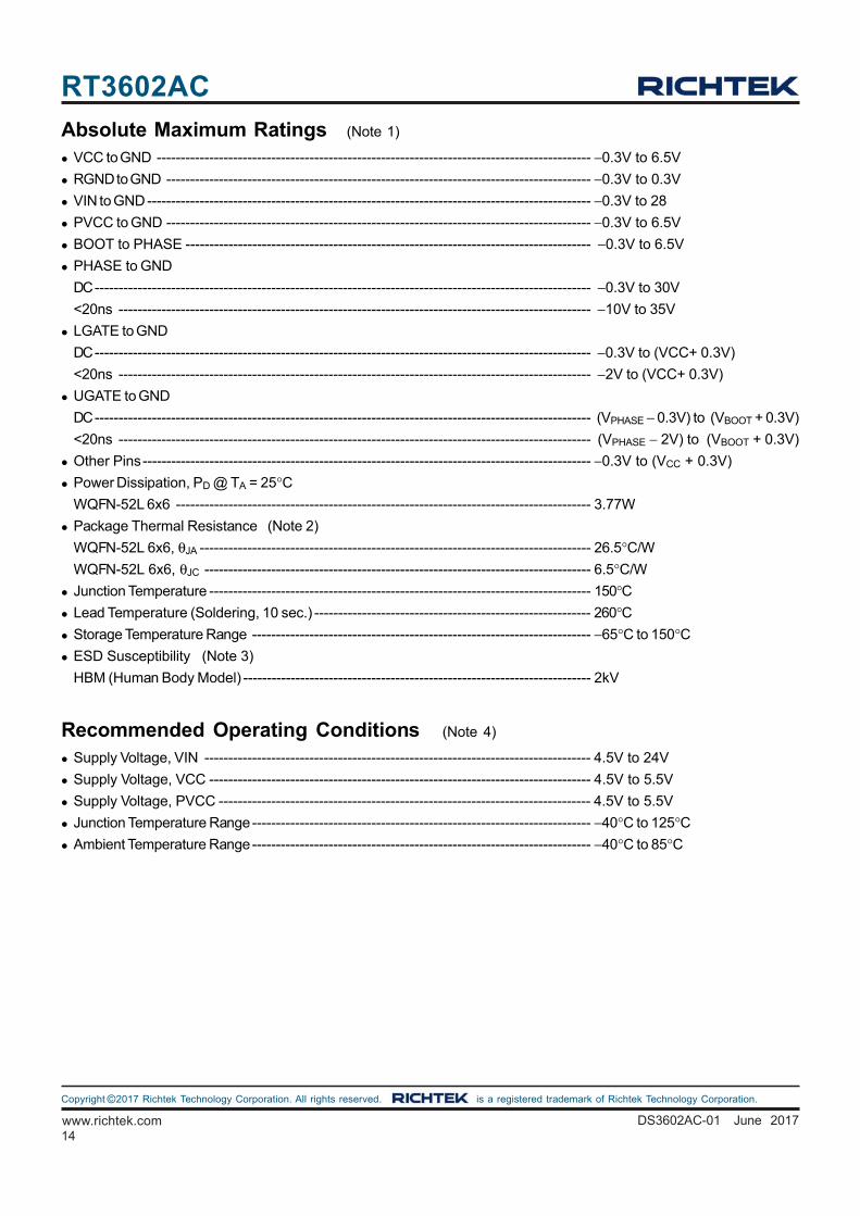
Recommended Operating Conditions (Note 4)
Supply Voltage, VIN --------------------------------------------------------------------------------- 4.5V to 24V
Supply Voltage, VCC -------------------------------------------------------------------------------- 4.5V to 5.5V
Supply Voltage, PVCC ------------------------------------------------------------------------------ 4.5V to 5.5V
Junction Temperature Range----------------------------------------------------------------------- −40°C to 125°C Ambient Temperature Range----------------------------------------------------------------------- −40°C to 85°C
Absolute Maximum Ratings (Note 1)
VCC to GND ------------------------------------------------------------------------------------------- −0.3V to 6.5V
RGND to GND ----------------------------------------------------------------------------------------- −0.3V to 0.3V
VIN to GND--------------------------------------------------------------------------------------------- −0.3V to 28
PVCC to GND ----------------------------------------------------------------------------------------- −0.3V to 6.5V
BOOT to PHASE ------------------------------------------------------------------------------------- −0.3V to 6.5V
PHASE to GND
DC-------------------------------------------------------------------------------------------------------- −0.3V to 30V
<20ns --------------------------------------------------------------------------------------------------- −10V to 35V
LGATE to GND
DC-------------------------------------------------------------------------------------------------------- −0.3V to (VCC+ 0.3V)
<20ns --------------------------------------------------------------------------------------------------- −2V to (VCC+ 0.3V)
UGATE to GND
DC-------------------------------------------------------------------------------------------------------- (VPHASE − 0.3V) to (VBOOT + 0.3V)
<20ns --------------------------------------------------------------------------------------------------- (VPHASE − 2V) to (VBOOT + 0.3V)
Other Pins---------------------------------------------------------------------------------------------- −0.3V to (VCC + 0.3V)
Power Dissipation, PD @ TA = 25°C
WQFN-52L 6x6 --------------------------------------------------------------------------------------- 3.77W
Package Thermal Resistance (Note 2)
WQFN-52L 6x6, θJA ---------------------------------------------------------------------------------- 26.5°C/W
WQFN-52L 6x6, θJC --------------------------------------------------------------------------------- 6.5°C/W
Junction Temperature -------------------------------------------------------------------------------- 150°C Lead Temperature (Soldering, 10 sec.) ---------------------------------------------------------- 260°C Storage Temperature Range ----------------------------------------------------------------------- −65°C to 150°C ESD Susceptibility (Note 3)
HBM (Human Body Model) ------------------------------------------------------------------------- 2kV
15
RT3602AC
DS3602AC-01 June 2017 www.richtek.com
©Copyright 2017 Richtek Technology Corporation. All rights reserved. is a registered trademark of Richtek Technology Corporation.
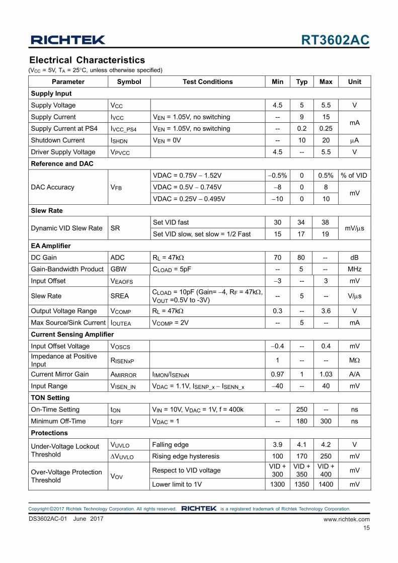
Electrical Characteristics(VCC = 5V, TA = 25°C, unless otherwise specified)
Parameter Symbol Test Conditions Min Typ Max Unit
Supply Input
Supply Voltage VCC 4.5 5 5.5 V
Supply Current IVCC VEN = 1.05V, no switching -- 9 15 mA
Supply Current at PS4 IVCC_PS4 VEN = 1.05V, no switching -- 0.2 0.25
Shutdown Current ISHDN VEN = 0V -- 10 20 A
Driver Supply Voltage VPVCC 4.5 -- 5.5 V
Reference and DAC
DAC Accuracy VFB
VDAC = 0.75V 1.52V 0.5% 0 0.5% % of VID
VDAC = 0.5V 0.745V 8 0 8 mV
VDAC = 0.25V 0.495V 10 0 10
Slew Rate
Dynamic VID Slew Rate SR Set VID fast 30 34 38
mV/s Set VID slow, set slow = 1/2 Fast 15 17 19
EA Amplifier
DC Gain ADC RL = 47k 70 80 -- dB
Gain-Bandwidth Product GBW CLOAD = 5pF -- 5 -- MHz
Input Offset VEAOFS 3 -- 3 mV
Slew Rate SREA CLOAD = 10pF (Gain= 4, RF = 47k, VOUT =0.5V to -3V)
-- 5 -- V/s
Output Voltage Range VCOMP RL = 47k 0.3 -- 3.6 V
Max Source/Sink Current IOUTEA VCOMP = 2V -- 5 -- mA
Current Sensing Amplifier
Input Offset Voltage VOSCS 0.4 -- 0.4 mV
Impedance at Positive Input
RISENxP 1 -- -- M
Current Mirror Gain AMIRROR IIMON/ISENxN 0.97 1 1.03 A/A
Input Range VISEN_IN VDAC = 1.1V, ISENP_x ISENN_x 40 -- 40 mV
TON Setting
On-Time Setting tON VIN = 10V, VDAC = 1V, f = 400k -- 250 -- ns
Minimum Off-Time tOFF VDAC = 1 -- 180 300 ns
Protections
Under-Voltage Lockout Threshold
VUVLO Falling edge 3.9 4.1 4.2 V
VUVLO Rising edge hysteresis 100 170 250 mV
Over-Voltage Protection Threshold
VOV Respect to VID voltage
VID + 300
VID + 350
VID + 400
mV
Lower limit to 1V 1300 1350 1400 mV
16
RT3602AC
www.richtek.com DS3602AC-01 June 2017
©Copyright 2017 Richtek Technology Corporation. All rights reserved. is a registered trademark of Richtek Technology Corporation.
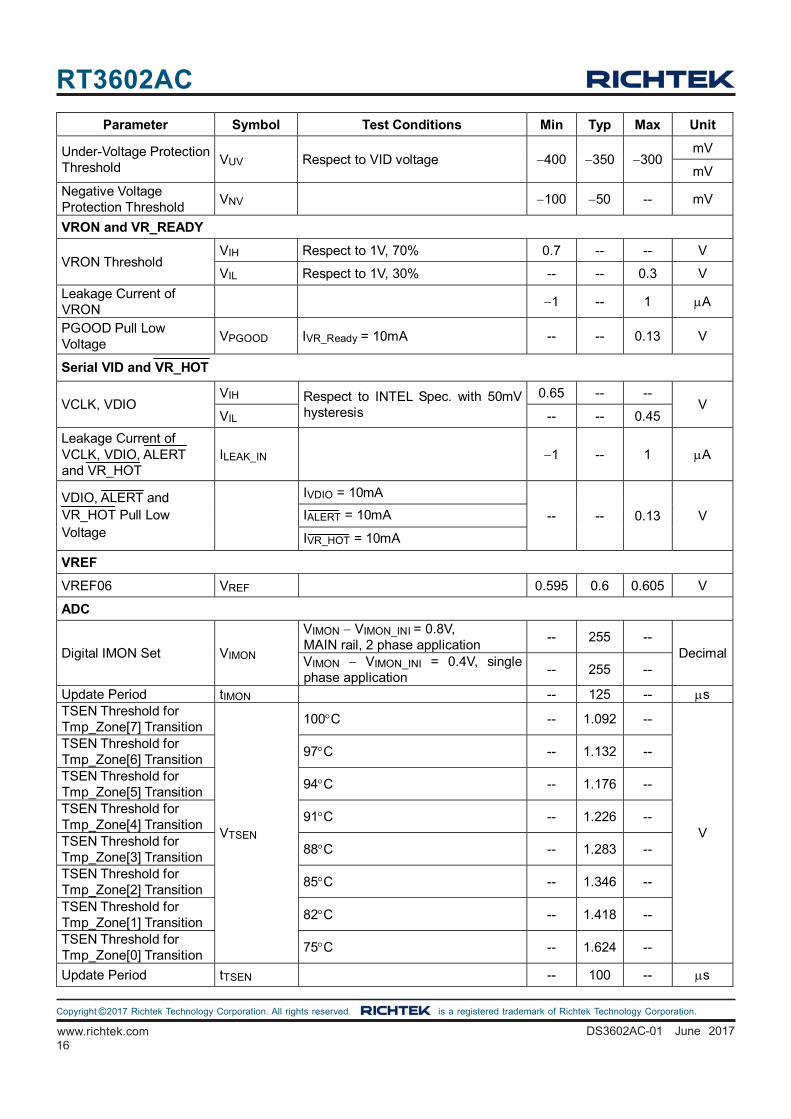
Parameter Symbol Test Conditions Min Typ Max Unit
Under-Voltage Protection Threshold
VUV Respect to VID voltage 400 350 300 mV
mV
Negative Voltage Protection Threshold
VNV 100 50 -- mV
VRON and VR_READY
VRON Threshold VIH Respect to 1V, 70% 0.7 -- -- V
VIL Respect to 1V, 30% -- -- 0.3 V
Leakage Current of VRON
1 -- 1 A
PGOOD Pull Low Voltage
VPGOOD IVR_Ready = 10mA -- -- 0.13 V
Serial VID and VR_HOT
VCLK, VDIO VIH Respect to INTEL Spec. with 50mV
hysteresis
0.65 -- -- V
VIL -- -- 0.45
Leakage Current of VCLK, VDIO, ALERT and VR_HOT
ILEAK_IN 1 -- 1 A
VDIO, ALERT and VR_HOT Pull Low Voltage
IVDIO = 10mA
-- -- 0.13 V IALERT = 10mA
IVR_HOT = 10mA
VREF
VREF06 VREF 0.595 0.6 0.605 V
ADC
Digital IMON Set VIMON
VIMON VIMON_INI = 0.8V, MAIN rail, 2 phase application
-- 255 -- Decimal
VIMON VIMON_INI = 0.4V, single phase application
-- 255 --
Update Period tIMON -- 125 -- s TSEN Threshold for Tmp_Zone[7] Transition
VTSEN
100C -- 1.092 --
V
TSEN Threshold for Tmp_Zone[6] Transition
97C -- 1.132 --
TSEN Threshold for Tmp_Zone[5] Transition
94C -- 1.176 --
TSEN Threshold for Tmp_Zone[4] Transition
91C -- 1.226 --
TSEN Threshold for Tmp_Zone[3] Transition
88C -- 1.283 --
TSEN Threshold for Tmp_Zone[2] Transition
85C -- 1.346 --
TSEN Threshold for Tmp_Zone[1] Transition
82C -- 1.418 --
TSEN Threshold for Tmp_Zone[0] Transition
75C -- 1.624 --
Update Period tTSEN -- 100 -- s
17
RT3602AC
DS3602AC-01 June 2017 www.richtek.com
©Copyright 2017 Richtek Technology Corporation. All rights reserved. is a registered trademark of Richtek Technology Corporation.
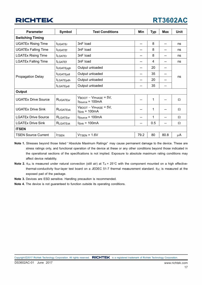
Note 1. Stresses beyond those listed “Absolute Maximum Ratings” may cause permanent damage to the device. These are
stress ratings only, and functional operation of the device at these or any other conditions beyond those indicated in
the operational sections of the specifications is not implied. Exposure to absolute maximum rating conditions may
affect device reliability.
Note 2. θJA is measured under natural convection (still air) at TA = 25°C with the component mounted on a high effective-
thermal-conductivity four-layer test board on a JEDEC 51-7 thermal measurement standard. θJC is measured at the
exposed pad of the package.
Note 3. Devices are ESD sensitive. Handling precaution is recommended.
Note 4. The device is not guaranteed to function outside its operating conditions.
Parameter Symbol Test Conditions Min Typ Max Unit
Switching Timing
UGATEx Rising Time tUGATEr 3nF load -- 8 -- ns
UGATEx Falling Time tUGATEf 3nF load -- 8 -- ns
LGATEx Rising Time tLGATEr 3nF load -- 8 -- ns
LGATEx Falling Time tLGATEf 3nF load -- 4 -- ns
Propagation Delay
tUGATEpgh Output unloaded -- 20 --
ns tUGATEpdl Output unloaded -- 35 --
tLGATEpdh Output unloaded -- 20 --
tLGATEpdl Output unloaded -- 35 --
Output
UGATEx Drive Source RUGATEsr VBOOT VPHASE = 5V, ISource = 100mA
-- 1 --
UGATEx Drive Sink RUGATEsk VBOOT VPHASE = 5V, ISink = 100mA
-- 1 --
LGATEx Drive Source RLGATEsr ISource = 100mA -- 1 --
LGATEx Drive Sink RLGATEsk ISink = 100mA -- 0.5 --
ITSEN
TSEN Source Current ITSEN VTSEN = 1.6V 79.2 80 80.8 A
18
RT3602AC
www.richtek.com DS3602AC-01 June 2017
©Copyright 2017 Richtek Technology Corporation. All rights reserved. is a registered trademark of Richtek Technology Corporation.
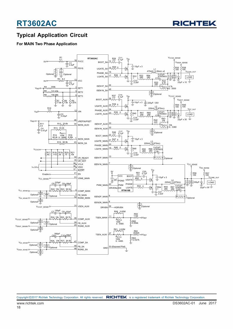
Typical Application Circuit
For MAIN Two Phase Application
RT3602AC
13 VCC5V
50 PSYS
EN41
VIN
VIN
LOAD
VSSGT_SENSE
VGT_OUT
VCCGT_SENSE
7
10
VCC
PWM
BOOT
UGATE
PHASE
LGATE
PGND
RT9610B
ISEN2N_MAIN
ISEN2P_MAIN
PWM_MAIN 40
9
8
ENDRVEN
5VVIN
VIN
Optional
LOAD
VCORE_OUT
VSS_SENSE
VCC_SENSE
DRVEN39
DRVEN
RGND_AUXI29FB_AUXI28
COMP_AUXI30
Optional
Optional
Optional
VSSGT_SENSE
RGND_MAIN52FB_MAIN3
COMP_MAIN4
Optional
Optional
Optional
VSS_SENSE
VCC_SENSE
TSEN_MAIN11
RNTC4
VSEN_AUXI31
51
6
5
VSNE_MAIN
SET3
SET2
VREF2 SET1
VR_READY42
35
VCLK
VDIO
38
36
37
VCCIO
To CPU
12 VINVIN
VREF06/PSET
IMON_AUXI
IMON_MAIN
34
1
46
VR_HOT
ALERT
GND53 (Exposed Pad)
Enable
IMON_SA43
TSEN_AUXI27
RNTC5
RGND_SA48FB_SA49
COMP_SA47
VSSSA_SENSE
VSA_SENSE
VCCGT_SENSE
VCCSA_OUT
VSSSA_SENSE
VCCSA_SENSE
18 PVCC5V
BOOT_MAIN
UGATE_MAIN
PHASE_MAIN
LGATE_MAIN
ISEN1P_MAIN
ISEN1N_MAIN
Optional
LOAD
19
20
21
22
32
33
BOOT_AUXI
UGATE_AUXI
PHASE_AUXI
LGATE_AUXI
ISEN1P_AUXI
ISEN1N_AUXI
23
24
25
26
45
44
BOOT_SA
UGATE_SA
PHASE_SA
LGATE_SA
ISEN1P_SA
ISEN1N_SA
17
16
15
14
VCC_SENSE
VCCGT_SENSE
VREF
VREF
5.1R1
C12.2µF
Optional Optional
R3 8.2
C24.7µF
R4
R5
R6
200k
131.43k
156.98k
17.8kR7
7.6kR8
4.87kR9
R10
C30.22µF
1.2
RNTC1
VREF
3.9R11
C40.47µF
R12 33.6k
R13 33.2k
R1446.4k
100kß : 4485
R15 90.9k
R168.06k
R17NC
R18110
R1955
R2075
R2110k
C5 220pF C6 68pF
R22 10k R23 36.5k
C7150pF
C8 82pF
R24 10k R25 26.7k
OptionalOptional
Optional
C9390pF
C10 68pF
R26 10k R27 36.5k
R282.2
C110.1µF
R29 0
R30 0
RNTC2
10µF x 3
R311C123.3nF
R32280
L1470nH / 2.26m x2
0.47µF/X7R/0603
R33590
R344.7k
4.7kß : 3500
R35100
R36100
22µF x 10
R372.2
C140.1µF
R38 0
R39 0
10µF x 3
R401C153.3nF
R41295
220µF / 35V
RNTC3
L2220nH / 0.875m
0.47µF/X7R/0603
R42220
R4310k
10kß : 3380
C13
C16
R44100
R45100
22µF x 30
R462.2
C170.1µF
R47 0
R48 0
10µF x 3
R491C183.3nF
R50280
L3220nH / 0.875m
0.47µF/X7R/0603
C19
1µF
R512.2
C200.1µF
R52 0
R53 0
10µF x 3
R541
C213.3nF
L4220nH / 0.875m
R55280
0.47µF/X7R/0603C22
330µF
22µF x 30
R56100
R57100
R58 5.62M
100kß : 4485
R59112k
R609.554k
R61 5.62M
100kß : 4485
R6229.62k
R6312.527k
Optional
Optional
Optional
Optional
280
295
280
280
R64
R65
R66
R67
19
RT3602AC
DS3602AC-01 June 2017 www.richtek.com
©Copyright 2017 Richtek Technology Corporation. All rights reserved. is a registered trademark of Richtek Technology Corporation.
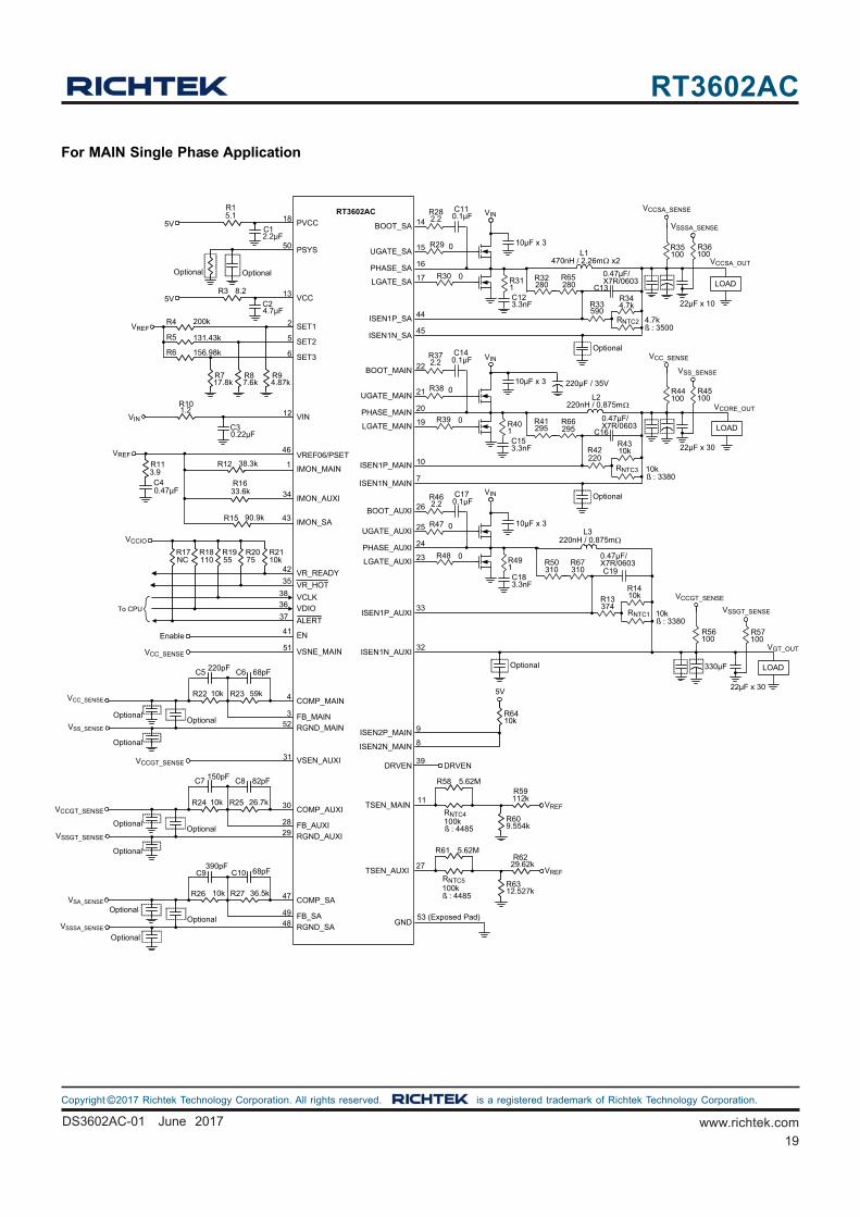
For MAIN Single Phase Application
RT3602AC
13 VCC5V
50 PSYS
EN41
VIN
VIN
LOAD
VSS_SENSE
VCORE_OUT
VCC_SENSE
32
33
ISEN2N_MAIN
ISEN2P_MAIN 9
8
VIN
LOAD
VGT_OUT
VSSGT_SENSE
VCCGT_SENSE
DRVEN39
DRVEN
RGND_AUXI29FB_AUXI28
COMP_AUXI30
Optional
Optional
Optional
VSSGT_SENSE
RGND_MAIN52FB_MAIN3
COMP_MAIN4
Optional
Optional
Optional
VSS_SENSE
VCC_SENSE
TSEN_MAIN11
RNTC4
VSEN_AUXI31
51
6
5
VSNE_MAIN
SET3
SET2
VREF2 SET1
VR_READY42
35
VCLK
VDIO
38
36
37
VCCIO
To CPU
12 VINVIN
VREF06/PSET
IMON_MAIN
IMON_AUXI
1
34
46
VR_HOT
ALERT
GND53 (Exposed Pad)
Enable
IMON_SA43
TSEN_AUXI27
RNTC5
RGND_SA48FB_SA49
COMP_SA47
VSSSA_SENSE
VSA_SENSE
VCCGT_SENSE
VCCSA_OUT
VSSSA_SENSE
VCCSA_SENSE
18 PVCC5V
BOOT_AUXI
UGATE_AUXI
PHASE_AUXI
LGATE_AUXI
ISEN1P_AUXI
ISEN1N_AUXI
LOAD
23
24
25
26
7
10
BOOT_MAIN
UGATE_MAIN
PHASE_MAIN
LGATE_MAIN
ISEN1P_MAIN
ISEN1N_MAIN
19
20
21
22
45
44
BOOT_SA
UGATE_SA
PHASE_SA
LGATE_SA
ISEN1P_SA
ISEN1N_SA
17
16
15
14
VCC_SENSE
VCCGT_SENSE
VREF
VREF
5.1R1
C12.2µF
Optional Optional
R3 8.2
C24.7µF
R4
R5
R6
200k
131.43k
156.98k
17.8kR7
7.6kR8
4.87kR9
R10
C30.22µF
1.2
VREF
3.9R11
C40.47µF
R12 38.3k
R15 90.9k
R1633.6k
R17NC
R18110
R1955
R2075
R2110k
C5220pF
C6 68pF
R22 10k R23 59k
C7150pF
C8 82pF
R24 10k R25 26.7k
OptionalOptional
Optional
C9390pF
C10 68pF
R26 10k R27 36.5k
R282.2
C110.1µF
R29 0
R30 0
RNTC2
10µF x 3
R311C123.3nF
R32280
L1
0.47µF/X7R/0603
R33590
R344.7k
4.7kß : 3500
R35100
R36100
22µF x 10
R372.2
C140.1µF
R38 0
R39 0
10µF x 3
R401C153.3nF
R41295
220µF / 35V
RNTC3
L2220nH / 0.875m
0.47µF/X7R/0603
R42220
R4310k
10kß : 3380
C13
C16
R44100
R45100
22µF x 30
R462.2
C170.1µF
R47 0
R48 0
10µF x 3
R491C183.3nF
R50310
L3
0.47µF/X7R/0603C19
330µF
22µF x 30
R56100
R57100
R58 5.62M
100kß : 4485
R59112k
R609.554k
R61 5.62M
100kß : 4485
R6229.62k
R6312.527k
Optional
Optional
Optional
RNTC1
R1410k
10kß : 3380
R13374
5V
R6410k
280
470nH / 2.26m x2
295
310
220nH / 0.875m
R65
R66
R67
20
RT3602AC
www.richtek.com DS3602AC-01 June 2017
©Copyright 2017 Richtek Technology Corporation. All rights reserved. is a registered trademark of Richtek Technology Corporation.
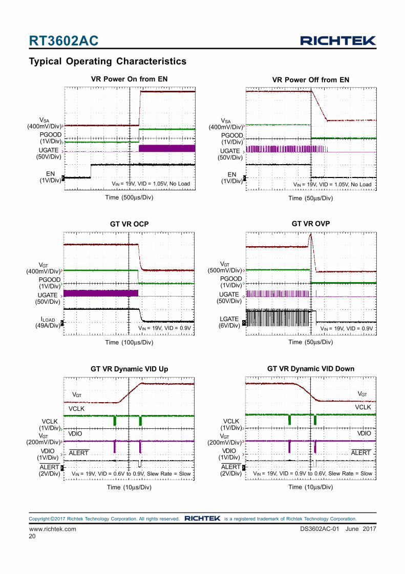
Typical Operating Characteristics
Time (500μs/Div)
VR Power On from EN
VIN = 19V, VID = 1.05V, No Load
UGATE(50V/Div)
VSA(400mV/Div)
PGOOD(1V/Div)
EN(1V/Div)
Time (100μs/Div)
GT VR OCP
UGATE(50V/Div)
VGT(400mV/Div)
PGOOD(1V/Div)
ILOAD(49A/Div) VIN = 19V, VID = 0.9V
Time (10μs/Div)
GT VR Dynamic VID Up
VIN = 19V, VID = 0.6V to 0.9V, Slew Rate = Slow
VDIO(1V/Div)
VGT(200mV/Div)
VCLK(1V/Div)
ALERT(2V/Div)
VGT
VCLK
VDIO
ALERT
Time (10μs/Div)
GT VR Dynamic VID Down
VIN = 19V, VID = 0.9V to 0.6V, Slew Rate = Slow
VDIO(1V/Div)
VGT(200mV/Div)
VCLK(1V/Div)
ALERT(2V/Div)
VGT
VCLK
VDIO
ALERT
Time (50μs/Div)
GT VR OVP
VIN = 19V, VID = 0.9V
UGATE(50V/Div)
VGT(500mV/Div)
PGOOD(1V/Div)
LGATE(6V/Div)
Time (50μs/Div)
VR Power Off from EN
VIN = 19V, VID = 1.05V, No Load
UGATE(50V/Div)
VSA(400mV/Div)
PGOOD(1V/Div)
EN(1V/Div)
21
RT3602AC
DS3602AC-01 June 2017 www.richtek.com
©Copyright 2017 Richtek Technology Corporation. All rights reserved. is a registered trademark of Richtek Technology Corporation.
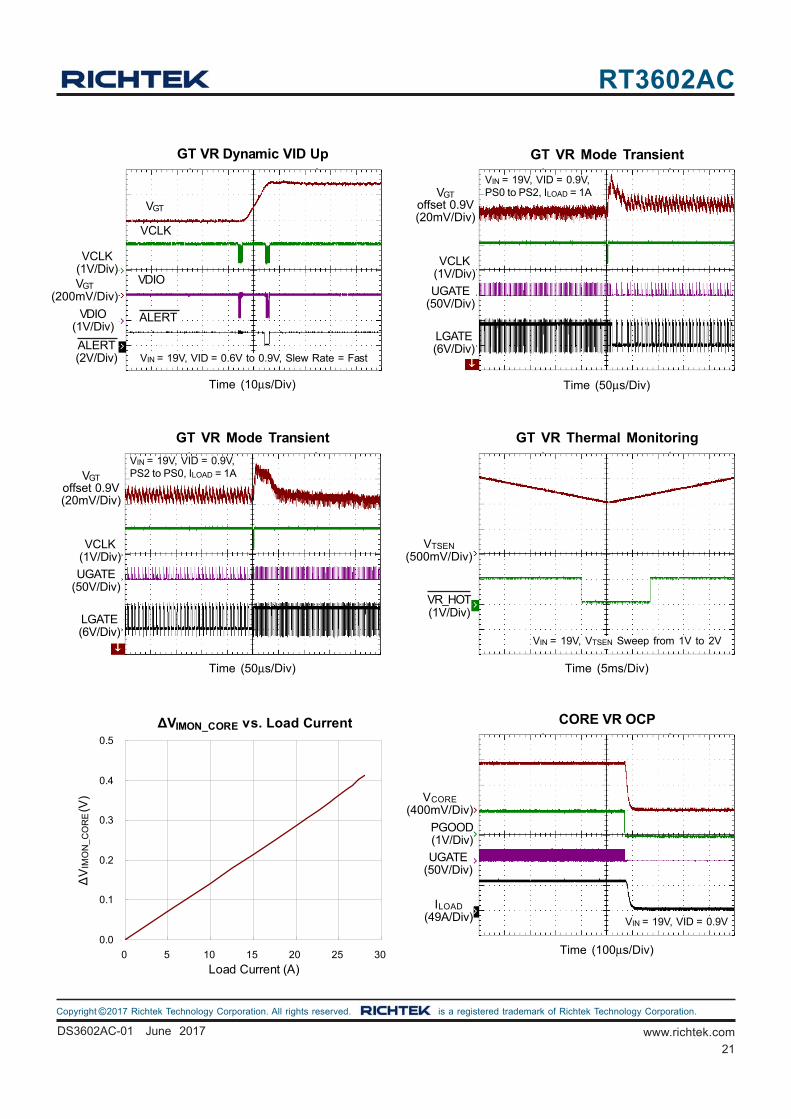
∆VIMON_CORE vs. Load Current
0.0
0.1
0.2
0.3
0.4
0.5
0 5 10 15 20 25 30
Load Current (A)
∆V
IMO
N_
CO
RE
(V)
Time (100μs/Div)
CORE VR OCP
UGATE(50V/Div)
VCORE(400mV/Div)
PGOOD(1V/Div)
ILOAD(49A/Div) VIN = 19V, VID = 0.9V
Time (10μs/Div)
GT VR Dynamic VID Up
VIN = 19V, VID = 0.6V to 0.9V, Slew Rate = Fast
VDIO(1V/Div)
VGT(200mV/Div)
VCLK(1V/Div)
ALERT(2V/Div)
VGT
VCLK
VDIO
ALERT
Time (50μs/Div)
GT VR Mode Transient
VIN = 19V, VID = 0.9V,PS2 to PS0, ILOAD = 1A
UGATE(50V/Div)
VGToffset 0.9V(20mV/Div)
VCLK(1V/Div)
LGATE(6V/Div)
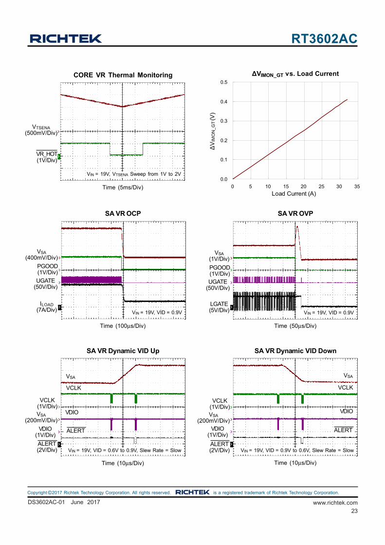
Time (5ms/Div)
GT VR Thermal Monitoring
VIN = 19V, VTSEN Sweep from 1V to 2V
VTSEN(500mV/Div)
VR_HOT(1V/Div)
Time (50μs/Div)
GT VR Mode Transient
VIN = 19V, VID = 0.9V,PS0 to PS2, ILOAD = 1A
UGATE(50V/Div)
VGToffset 0.9V(20mV/Div)
VCLK(1V/Div)
LGATE(6V/Div)
22
RT3602AC
www.richtek.com DS3602AC-01 June 2017
©Copyright 2017 Richtek Technology Corporation. All rights reserved. is a registered trademark of Richtek Technology Corporation.
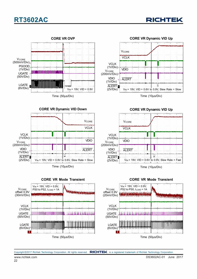
Time (50μs/Div)
CORE VR Mode Transient
VIN = 19V, VID = 0.9V,PS2 to PS0, ILOAD = 1A
UGATE(50V/Div)
VCOREoffset 0.9V(20mV/Div)
VCLK(1V/Div)
LGATE(6V/Div)
Time (10μs/Div)
CORE VR Dynamic VID Up
VIN = 19V, VID = 0.6V to 0.9V, Slew Rate = Slow
VDIO(1V/Div)
VCORE(200mV/Div)
VCLK(1V/Div)
ALERT(2V/Div)
VCORE
VCLK
VDIO
ALERT
Time (50μs/Div)
CORE VR OVP
VIN = 19V, VID = 0.9V
UGATE(50V/Div)
VCORE(500mV/Div)
PGOOD(1V/Div)
LGATE(6V/Div)
Time (50μs/Div)
CORE VR Mode Transient
VIN = 19V, VID = 0.9V,PS0 to PS2, ILOAD = 1A
UGATE(50V/Div)
VCOREoffset 0.9V(30mV/Div)
VCLK(1V/Div)
LGATE(6V/Div)
CORE VR Dynamic VID Down
VIN = 19V, VID = 0.9V to 0.6V, Slew Rate = Slow
VDIO(1V/Div)
VCORE(200mV/Div)
VCLK(1V/Div)
ALERT(2V/Div)
VCLK
VDIO
ALERT
Time (10μs/Div)
VCORE
Time (10μs/Div)
CORE VR Dynamic VID Up
VIN = 19V, VID = 0.6V to 0.9V, Slew Rate = Fast
VDIO(1V/Div)
VCORE(200mV/Div)
VCLK(1V/Div)
ALERT(2V/Div)
VCLK
VDIO
ALERT
VCORE
23
RT3602AC
DS3602AC-01 June 2017 www.richtek.com
©Copyright 2017 Richtek Technology Corporation. All rights reserved. is a registered trademark of Richtek Technology Corporation.
∆VIMON_GT vs. Load Current
0.0
0.1
0.2
0.3
0.4
0.5
0 5 10 15 20 25 30 35
Load Current (A)
∆V
IMO
N_
GT
(V)
Time (5ms/Div)
CORE VR Thermal Monitoring
VIN = 19V, VTSENA Sweep from 1V to 2V
VTSENA(500mV/Div)
VR_HOT(1V/Div)
Time (100μs/Div)
SA VR OCP
UGATE(50V/Div)
VSA(400mV/Div)
PGOOD(1V/Div)
ILOAD(7A/Div) VIN = 19V, VID = 0.9V
Time (50μs/Div)
SA VR OVP
VIN = 19V, VID = 0.9V
UGATE(50V/Div)
VSA(1V/Div)
PGOOD(1V/Div)
LGATE(5V/Div)
SA VR Dynamic VID Down
VIN = 19V, VID = 0.9V to 0.6V, Slew Rate = Slow
VDIO(1V/Div)
VSA(200mV/Div)
VCLK(1V/Div)
ALERT(2V/Div)
VSA
VCLK
VDIO
ALERT
Time (10μs/Div)Time (10μs/Div)
SA VR Dynamic VID Up
VIN = 19V, VID = 0.6V to 0.9V, Slew Rate = Slow
VDIO(1V/Div)
VSA(200mV/Div)
VCLK(1V/Div)
ALERT(2V/Div)
VSA
VCLK
VDIO
ALERT
24
RT3602AC
www.richtek.com DS3602AC-01 June 2017
©Copyright 2017 Richtek Technology Corporation. All rights reserved. is a registered trademark of Richtek Technology Corporation.
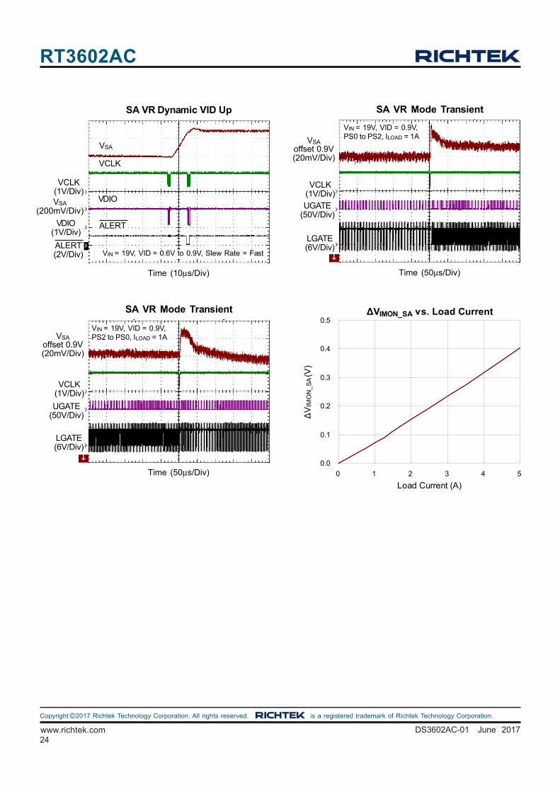
∆VIMON_SA vs. Load Current
0.0
0.1
0.2
0.3
0.4
0.5
0 1 2 3 4 5
Load Current (A)
∆V
IMO
N_
SA
(V)
Time (50μs/Div)
SA VR Mode Transient
VIN = 19V, VID = 0.9V,PS2 to PS0, ILOAD = 1A
UGATE(50V/Div)
VSAoffset 0.9V(20mV/Div)
VCLK(1V/Div)
LGATE(6V/Div)
Time (10μs/Div)
SA VR Dynamic VID Up
VIN = 19V, VID = 0.6V to 0.9V, Slew Rate = Fast
VDIO(1V/Div)
VSA(200mV/Div)
VCLK(1V/Div)
ALERT(2V/Div)
VSA
VCLK
VDIO
ALERT
Time (50μs/Div)
SA VR Mode Transient
VIN = 19V, VID = 0.9V,PS0 to PS2, ILOAD = 1A
UGATE(50V/Div)
VSAoffset 0.9V(20mV/Div)
VCLK(1V/Div)
LGATE(6V/Div)
25
RT3602AC
DS3602AC-01 June 2017 www.richtek.com
©Copyright 2017 Richtek Technology Corporation. All rights reserved. is a registered trademark of Richtek Technology Corporation.
Applications information
The RT3602AC includes three voltage rails : a 2/1 phase
synchronous Buck controller, the MAIN VR, a single
multiphase synchronous Buck controller, the auxiliary VR,
and a single phase synchronous Buck controller, the
VCCSA VR, designed to meet Intel IMVP8 compatible
CPUs specification with a serial SVID control interface.
The controller uses an ADC to implement all kinds of
settings to save total pin number for easy use and
increasing PCB space utilization. The RT3602AC is used
in notebooks, desktop computers and servers.
General loop Function
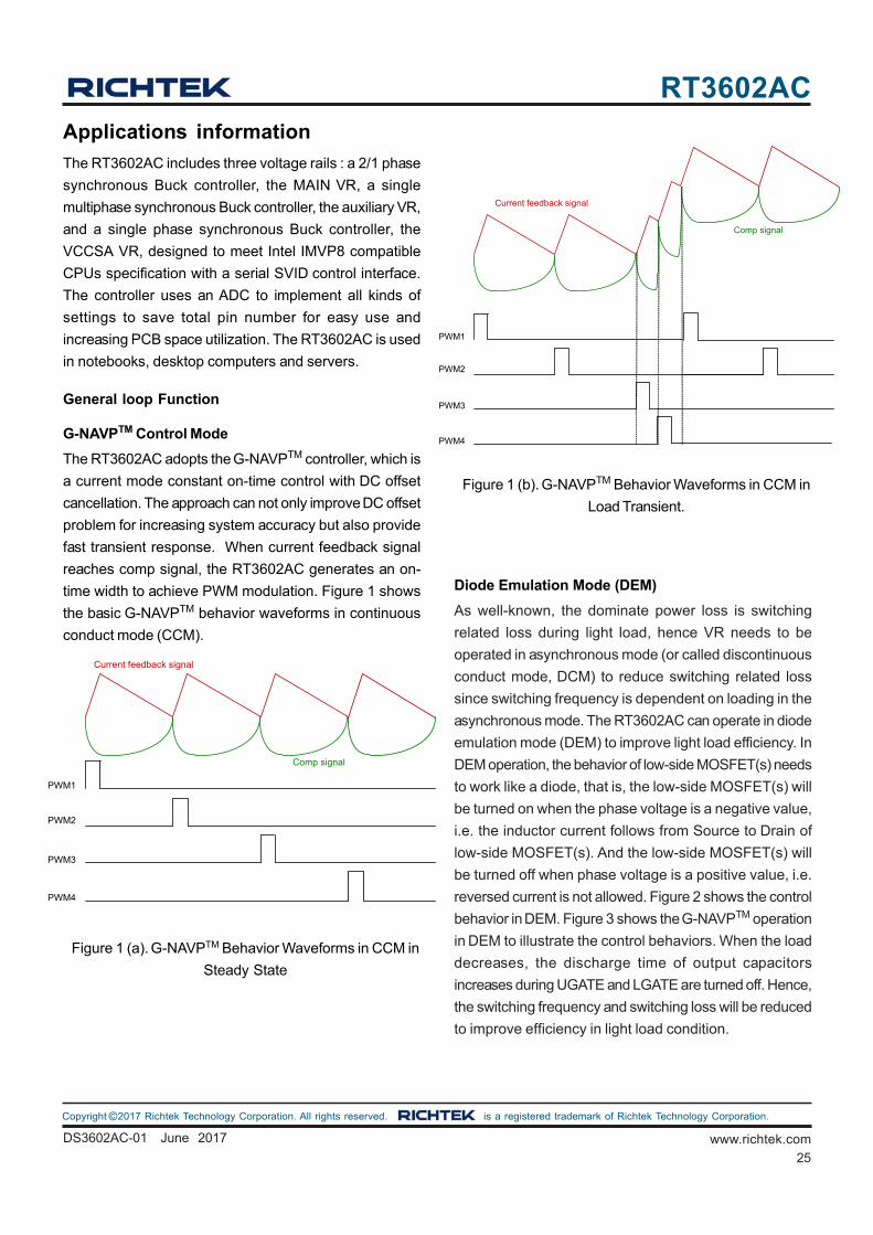
G-NAVPTM Control Mode
The RT3602AC adopts the G-NAVPTM controller, which is
a current mode constant on-time control with DC offset
cancellation. The approach can not only improve DC offset
problem for increasing system accuracy but also provide
fast transient response. When current feedback signal
reaches comp signal, the RT3602AC generates an on-
time width to achieve PWM modulation. Figure 1 shows
the basic G-NAVPTM behavior waveforms in continuous
conduct mode (CCM).
Figure 1 (a). G-NAVPTM Behavior Waveforms in CCM in
Steady State
PWM1
PWM2
PWM3
PWM4
Current feedback signal
Comp signal
Figure 1 (b). G-NAVPTM Behavior Waveforms in CCM in
Load Transient.
PWM1
PWM2
PWM3
PWM4
Current feedback signal
Comp signal
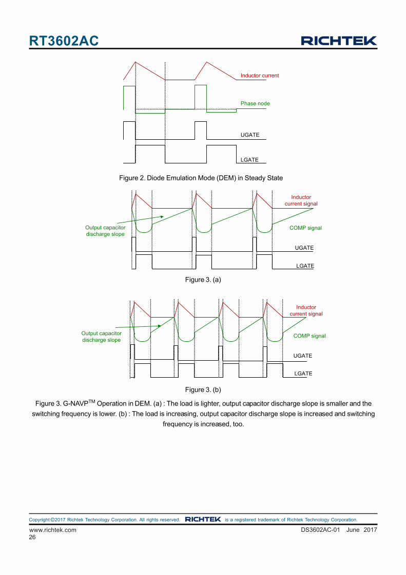
Diode Emulation Mode (DEM)
As well-known, the dominate power loss is switching
related loss during light load, hence VR needs to be
operated in asynchronous mode (or called discontinuous
conduct mode, DCM) to reduce switching related loss
since switching frequency is dependent on loading in the
asynchronous mode. The RT3602AC can operate in diode
emulation mode (DEM) to improve light load efficiency. In
DEM operation, the behavior of low-side MOSFET(s) needs
to work like a diode, that is, the low-side MOSFET(s) will
be turned on when the phase voltage is a negative value,
i.e. the inductor current follows from Source to Drain of
low-side MOSFET(s). And the low-side MOSFET(s) will
be turned off when phase voltage is a positive value, i.e.
reversed current is not allowed. Figure 2 shows the control
behavior in DEM. Figure 3 shows the G-NAVPTM operation
in DEM to illustrate the control behaviors. When the load
decreases, the discharge time of output capacitors
increases during UGATE and LGATE are turned off. Hence,
the switching frequency and switching loss will be reduced
to improve efficiency in light load condition.
26
RT3602AC
www.richtek.com DS3602AC-01 June 2017
©Copyright 2017 Richtek Technology Corporation. All rights reserved. is a registered trademark of Richtek Technology Corporation.
Figure 2. Diode Emulation Mode (DEM) in Steady State
Figure 3. G-NAVPTM Operation in DEM. (a) : The load is lighter, output capacitor discharge slope is smaller and the
switching frequency is lower. (b) : The load is increasing, output capacitor discharge slope is increased and switching
frequency is increased, too.
Inductor current
Phase node
UGATE
LGATE
Output capacitor discharge slope
UGATE
LGATE
COMP signal
Inductor current signal
Output capacitor discharge slope
UGATE
LGATE
COMP signal
Inductor current signal
Figure 3. (a)
Figure 3. (b)
27
RT3602AC
DS3602AC-01 June 2017 www.richtek.com
©Copyright 2017 Richtek Technology Corporation. All rights reserved. is a registered trademark of Richtek Technology Corporation.
Phase Interleaving Function
The RT3602AC is a multi-output controller, the MAIN rail
of the RT3602AC has a phase interleaving function, 180
degree phase shift for 2-phase operation which can help
reduce output voltage ripple and EMI problem.
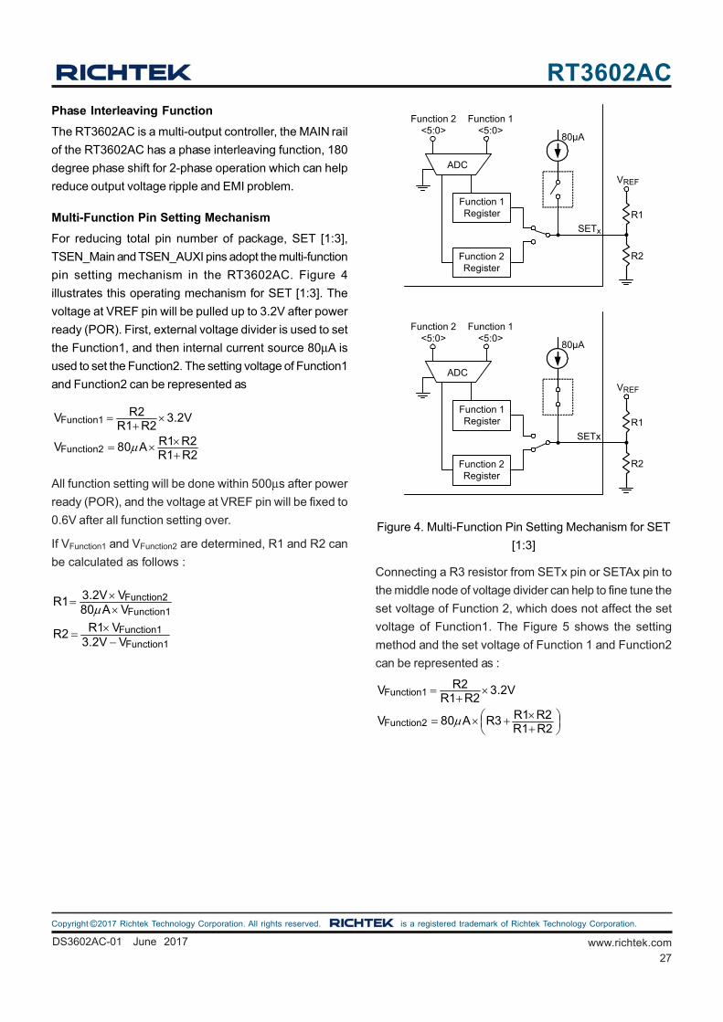
Multi-Function Pin Setting Mechanism
For reducing total pin number of package, SET [1:3],
TSEN_Main and TSEN_AUXI pins adopt the multi-function
pin setting mechanism in the RT3602AC. Figure 4
illustrates this operating mechanism for SET [1:3]. The
voltage at VREF pin will be pulled up to 3.2V after power
ready (POR). First, external voltage divider is used to set
the Function1, and then internal current source 80μA is
used to set the Function2. The setting voltage of Function1
and Function2 can be represented as
Function1
Function2
R2V 3.2VR1 R2
R1 R2V 80 ΑR1 R2
All function setting will be done within 500μs after power
ready (POR), and the voltage at VREF pin will be fixed to
0.6V after all function setting over.
If VFunction1 and VFunction2 are determined, R1 and R2 can
be calculated as follows :
Function2
Function1
Function1
Function1
3.2V VR180 Α V
R1 VR23.2V V
Figure 4. Multi-Function Pin Setting Mechanism for SET
[1:3]
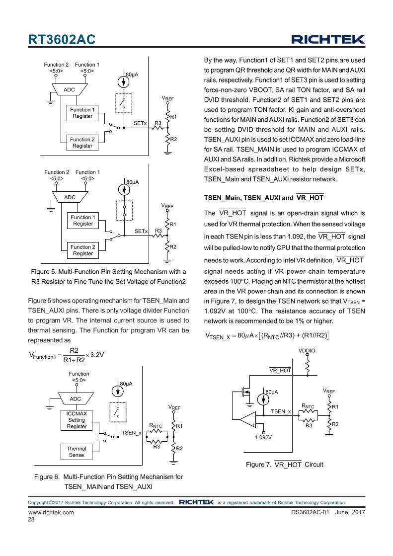
Connecting a R3 resistor from SETx pin or SETAx pin to
the middle node of voltage divider can help to fine tune the
set voltage of Function 2, which does not affect the set
voltage of Function1. The Figure 5 shows the setting
method and the set voltage of Function 1 and Function2
can be represented as :
Function1
Function2
R2V 3.2VR1 R2
R1 R2V 80 Α R3R1 R2
VREF
R1
R2
SETx
80µA
Function 1 Register
Function 2 Register
ADC
Function 1 <5:0>
Function 2 <5:0>
VREF
R1
R2
SETx
80µA
Function 1 Register
Function 2 Register
ADC
Function 1 <5:0>
Function 2 <5:0>
28
RT3602AC
www.richtek.com DS3602AC-01 June 2017
©Copyright 2017 Richtek Technology Corporation. All rights reserved. is a registered trademark of Richtek Technology Corporation.
Figure 5. Multi-Function Pin Setting Mechanism with a
R3 Resistor to Fine Tune the Set Voltage of Function2
Figure 6 shows operating mechanism for TSEN_Main and
TSEN_AUXI pins. There is only voltage divider Function
to program VR. The internal current source is used to
thermal sensing. The Function for program VR can be
represented as
Function1
R2V 3.2V
R1 R2
Figure 6. Multi-Function Pin Setting Mechanism for
TSEN_ MAIN and TSEN_ AUXI
By the way, Function1 of SET1 and SET2 pins are used
to program QR threshold and QR width for MAIN and AUXI
rails, respectively. Function1 of SET3 pin is used to setting
force-non-zero VBOOT, SA rail TON factor, and SA rail
DVID threshold. Function2 of SET1 and SET2 pins are
used to program TON factor, Ki gain and anti-overshoot
functions for MAIN and AUXI rails. Function2 of SET3 can
be setting DVID threshold for MAIN and AUXI rails.
TSEN_AUXI pin is used to set ICCMAX and zero load-line
for SA rail. TSEN_MAIN is used to program ICCMAX of
AUXI and SA rails. In addition, Richtek provide a Microsoft
Excel-based spreadsheet to help design SETx,
TSEN_Main and TSEN_AUXI resistor network.
TSEN_X NTCV 80 Α (R //R3) + (R1//R2)
VREF
R1
R2
80µA
Function 1 Register
Function 2 Register
ADC
Function 1 <5:0>
Function 2 <5:0>
R3SETx
VREF
R1
R2
80µA
Function 1 Register
Function 2 Register
ADC
Function 1 <5:0>
Function 2 <5:0>
R3SETx
VREF
R1
R2
TSEN_x
80µA
ICCMAX Setting
Register
Thermal Sense
ADC
Function <5:0>
R3
RNTC
TSEN_Main, TSEN_AUXI and VR_HOT
The VR_HOT signal is an open-drain signal which is
used for VR thermal protection. When the sensed voltage
in each TSEN pin is less than 1.092, the VR_HOT signal
will be pulled-low to notify CPU that the thermal protection
needs to work. According to Intel VR definition, VR_HOT
signal needs acting if VR power chain temperature
exceeds 100°C. Placing an NTC thermistor at the hottest
area in the VR power chain and its connection is shown
in Figure 7, to design the TSEN network so that VTSEN =
1.092V at 100°C. The resistance accuracy of TSEN
network is recommended to be 1% or higher.
Figure 7. VR_HOT Circuit
TSEN_xR1RNTC
-
+
1.092V
VDDIO
VR_HOT
80µA
R2R3
VREF
29
RT3602AC
DS3602AC-01 June 2017 www.richtek.com
©Copyright 2017 Richtek Technology Corporation. All rights reserved. is a registered trademark of Richtek Technology Corporation.
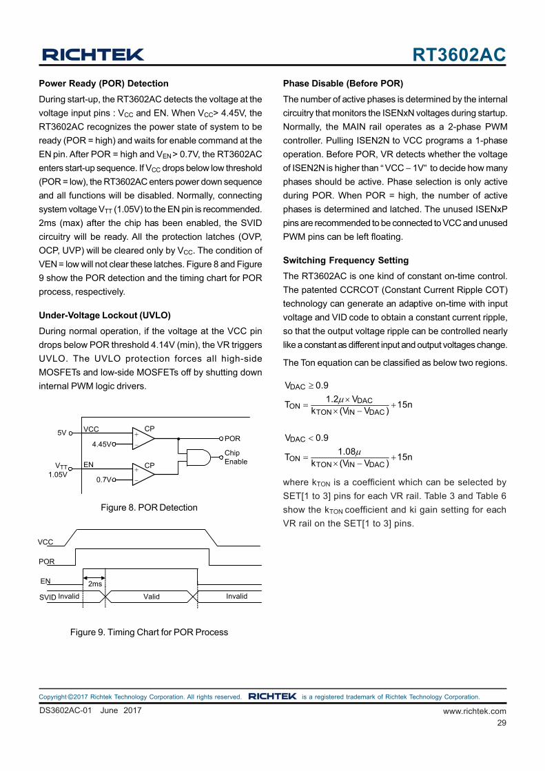
Power Ready (POR) Detection
During start-up, the RT3602AC detects the voltage at the
voltage input pins : VCC and EN. When VCC> 4.45V, the
RT3602AC recognizes the power state of system to be
ready (POR = high) and waits for enable command at the
EN pin. After POR = high and VEN > 0.7V, the RT3602AC
enters start-up sequence. If VCC drops below low threshold
(POR = low), the RT3602AC enters power down sequence
and all functions will be disabled. Normally, connecting
system voltage VTT (1.05V) to the EN pin is recommended.
2ms (max) after the chip has been enabled, the SVID
circuitry will be ready. All the protection latches (OVP,
OCP, UVP) will be cleared only by VCC. The condition of
VEN = low will not clear these latches. Figure 8 and Figure
9 show the POR detection and the timing chart for POR
process, respectively.
Under-Voltage Lockout (UVLO)
During normal operation, if the voltage at the VCC pin
drops below POR threshold 4.14V (min), the VR triggers
UVLO. The UVLO protection forces all high-side
MOSFETs and low-side MOSFETs off by shutting down
internal PWM logic drivers.
+
-
+
-
POR
Chip Enable
4.45V
0.7V
CP
CP
VCC
ENVTT1.05V
5V
Figure 8. POR Detection
VCC
POR
EN
SVID Invalid InvalidValid
2ms
Figure 9. Timing Chart for POR Process
Phase Disable (Before POR)
The number of active phases is determined by the internal
circuitry that monitors the ISENxN voltages during startup.
Normally, the MAIN rail operates as a 2-phase PWM
controller. Pulling ISEN2N to VCC programs a 1-phase
operation. Before POR, VR detects whether the voltage
of ISEN2N is higher than “VCC − 1V” to decide how many
phases should be active. Phase selection is only active
during POR. When POR = high, the number of active
phases is determined and latched. The unused ISENxP
pins are recommended to be connected to VCC and unused
PWM pins can be left floating.
Switching Frequency Setting
The RT3602AC is one kind of constant on-time control.
The patented CCRCOT (Constant Current Ripple COT)
technology can generate an adaptive on-time with input
voltage and VID code to obtain a constant current ripple,
so that the output voltage ripple can be controlled nearly
like a constant as different input and output voltages change.
The Ton equation can be classified as below two regions.
where kTON is a coefficient which can be selected by
SET[1 to 3] pins for each VR rail. Table 3 and Table 6
show the kTON coefficient and ki gain setting for each
VR rail on the SET[1 to 3] pins.
DAC
DACON
TON IN DAC
DAC
ONTON IN DAC
V 0.9
1.2 VT 15n
k (V V )
V 0.9
1.08T 15n
k (V V )
30
RT3602AC
www.richtek.com DS3602AC-01 June 2017
©Copyright 2017 Richtek Technology Corporation. All rights reserved. is a registered trademark of Richtek Technology Corporation.
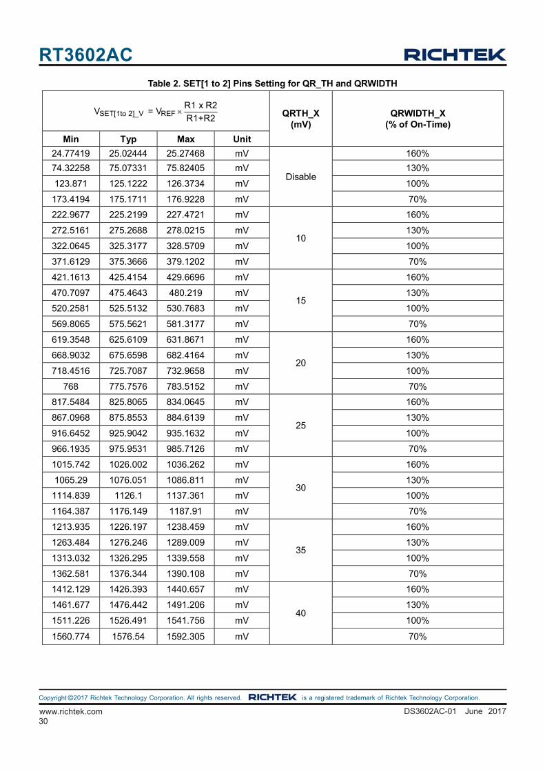
Table 2. SET[1 to 2] Pins Setting for QR_TH and QRWIDTH
SET[1to 2]_V REFR1 x R2
V = VR1+R2
QRTH_X (mV)
QRWIDTH_X (% of On-Time)
Min Typ Max Unit
24.77419 25.02444 25.27468 mV
Disable
160%
74.32258 75.07331 75.82405 mV 130%
123.871 125.1222 126.3734 mV 100%
173.4194 175.1711 176.9228 mV 70%
222.9677 225.2199 227.4721 mV
10
160%
272.5161 275.2688 278.0215 mV 130%
322.0645 325.3177 328.5709 mV 100%
371.6129 375.3666 379.1202 mV 70%
421.1613 425.4154 429.6696 mV
15
160%
470.7097 475.4643 480.219 mV 130%
520.2581 525.5132 530.7683 mV 100%
569.8065 575.5621 581.3177 mV 70%
619.3548 625.6109 631.8671 mV
20
160%
668.9032 675.6598 682.4164 mV 130%
718.4516 725.7087 732.9658 mV 100%
768 775.7576 783.5152 mV 70%
817.5484 825.8065 834.0645 mV
25
160%
867.0968 875.8553 884.6139 mV 130%
916.6452 925.9042 935.1632 mV 100%
966.1935 975.9531 985.7126 mV 70%
1015.742 1026.002 1036.262 mV
30
160%
1065.29 1076.051 1086.811 mV 130%
1114.839 1126.1 1137.361 mV 100%
1164.387 1176.149 1187.91 mV 70%
1213.935 1226.197 1238.459 mV
35
160%
1263.484 1276.246 1289.009 mV 130%
1313.032 1326.295 1339.558 mV 100%
1362.581 1376.344 1390.108 mV 70%
1412.129 1426.393 1440.657 mV
40
160%
1461.677 1476.442 1491.206 mV 130%
1511.226 1526.491 1541.756 mV 100%
1560.774 1576.54 1592.305 mV 70%
31
RT3602AC
DS3602AC-01 June 2017 www.richtek.com
©Copyright 2017 Richtek Technology Corporation. All rights reserved. is a registered trademark of Richtek Technology Corporation.
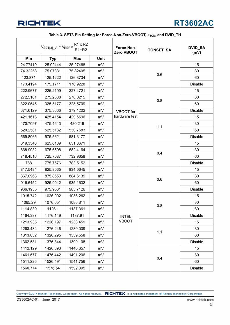
Table 3. SET3 Pin Setting for Force-Non-Zero-VBOOT, kTON, and DVID_TH
SET[3]_V REFR1 x R2
V = VR1+R2
Force-Non-Zero VBOOT
TONSET_SA DVID_SA
(mV)
Min Typ Max Unit
24.77419 25.02444 25.27468 mV
VBOOT for hardware test
0.6
15
74.32258 75.07331 75.82405 mV 30
123.871 125.1222 126.3734 mV 60
173.4194 175.1711 176.9228 mV Disable
222.9677 225.2199 227.4721 mV
0.8
15
272.5161 275.2688 278.0215 mV 30
322.0645 325.3177 328.5709 mV 60
371.6129 375.3666 379.1202 mV Disable
421.1613 425.4154 429.6696 mV
1.1
15
470.7097 475.4643 480.219 mV 30
520.2581 525.5132 530.7683 mV 60
569.8065 575.5621 581.3177 mV Disable
619.3548 625.6109 631.8671 mV
0.4
15
668.9032 675.6598 682.4164 mV 30
718.4516 725.7087 732.9658 mV 60
768 775.7576 783.5152 mV Disable
817.5484 825.8065 834.0645 mV
INTEL VBOOT
0.6
15
867.0968 875.8553 884.6139 mV 30
916.6452 925.9042 935.1632 mV 60
966.1935 975.9531 985.7126 mV Disable
1015.742 1026.002 1036.262 mV
0.8
15
1065.29 1076.051 1086.811 mV 30
1114.839 1126.1 1137.361 mV 60
1164.387 1176.149 1187.91 mV Disable
1213.935 1226.197 1238.459 mV
1.1
15
1263.484 1276.246 1289.009 mV 30
1313.032 1326.295 1339.558 mV 60
1362.581 1376.344 1390.108 mV Disable
1412.129 1426.393 1440.657 mV
0.4
15
1461.677 1476.442 1491.206 mV 30
1511.226 1526.491 1541.756 mV 60
1560.774 1576.54 1592.305 mV Disable
32
RT3602AC
www.richtek.com DS3602AC-01 June 2017
©Copyright 2017 Richtek Technology Corporation. All rights reserved. is a registered trademark of Richtek Technology Corporation.
For better efficiency of the given load range, the maximum
switching frequency is suggested to be :
SW(MAX)
ON_LS,maxLL
LS
ON_LS,max ON_HS,max ON_LS,maxIN(MAX) ON D ON,VAR D
LS HS LS
F
RIccTDCVID1 DCR N R
N n
R R RIccTDC IccTDCV T T T T
N n n N n
where FSW(MAX) is the maximum switching frequency, VID1
is the typical VID of application, VIN(MAX) is the maximum
application input voltage, IccTDC is the thermal design
current of application, N is the phase number. The
RON_HS,max is the maximum equivalent high-side RDS(ON) ,
and nHS is the number of high-side MOSFETs ; RON_LS,max
is the maximum equivalent low-side RDS(ON), and nLS is
the number of low-side MOSFETs. TD is the summation
of the high-side MOSFET delay time and the rising time,
TON, VAR is the TON variation value. DCR is the inductor
DCR, and RLL is the loadline setting. In addition, Richtek
provides a Microsoft Excel-based spreadsheet to help
design the RTON for the RT3602AC.
When load increases, on-time keeps constant. The off-
time width will be reduced so that loading can load more
power from input terminal to regulate output voltage.
Hence, the loading current usually increases in case the
switching frequency also increases. Higher switching
frequency operation can reduce power components' size
and PCB space, trading off the whole efficiency since
switching related loss increases, vice versa.
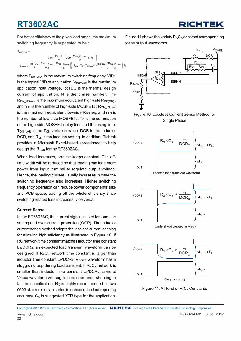
Current Sense
In the RT3602AC, the current signal is used for load-line
setting and over-current protection (OCP). The inductor
current sense method adopts the lossless current sensing
for allowing high efficiency as illustrated in Figure 10. If
RC network time constant matches inductor time constant
LX/DCRX, an expected load transient waveform can be
designed. If RXCX network time constant is larger than
inductor time constant LX/DCRX, VCORE waveform has a
sluggish droop during load transient. If RXCX network is
smaller than inductor time constant LX/DCRX, a worst
VCORE waveform will sag to create an undershooting to
fail the specification. RX is highly recommended as two
0603 size resistors in series to enhance the Iout reporting
accuracy. CX is suggested X7R type for the application.
Figure 10. Lossless Current Sense Method for
Single Phase
Expected load transient waveform
Undershoot created in VCORE
Sluggish droop
VCORE
IOUT
VCORE
IOUT
VCORE
IOUT
OUT LLI x R
OUTI
OUT LLI x R
OUTI
OUT LLI x R
OUTI
xx x
x
LR C =
DCR
xx x
x
LR C <
DCR
xx x
x
LR C >
DCR
Figure 11. All Kind of RxCx Constants
ISENP
ISENN
LX DCR
Cx
VCORE
+
-
RCS
ILx
IMON
RIMON
VREF
GM
RX1 RX2
RX
Figure 11 shows the variety RXCX constant corresponding
to the output waveforms.
33
RT3602AC
DS3602AC-01 June 2017 www.richtek.com
©Copyright 2017 Richtek Technology Corporation. All rights reserved. is a registered trademark of Richtek Technology Corporation.
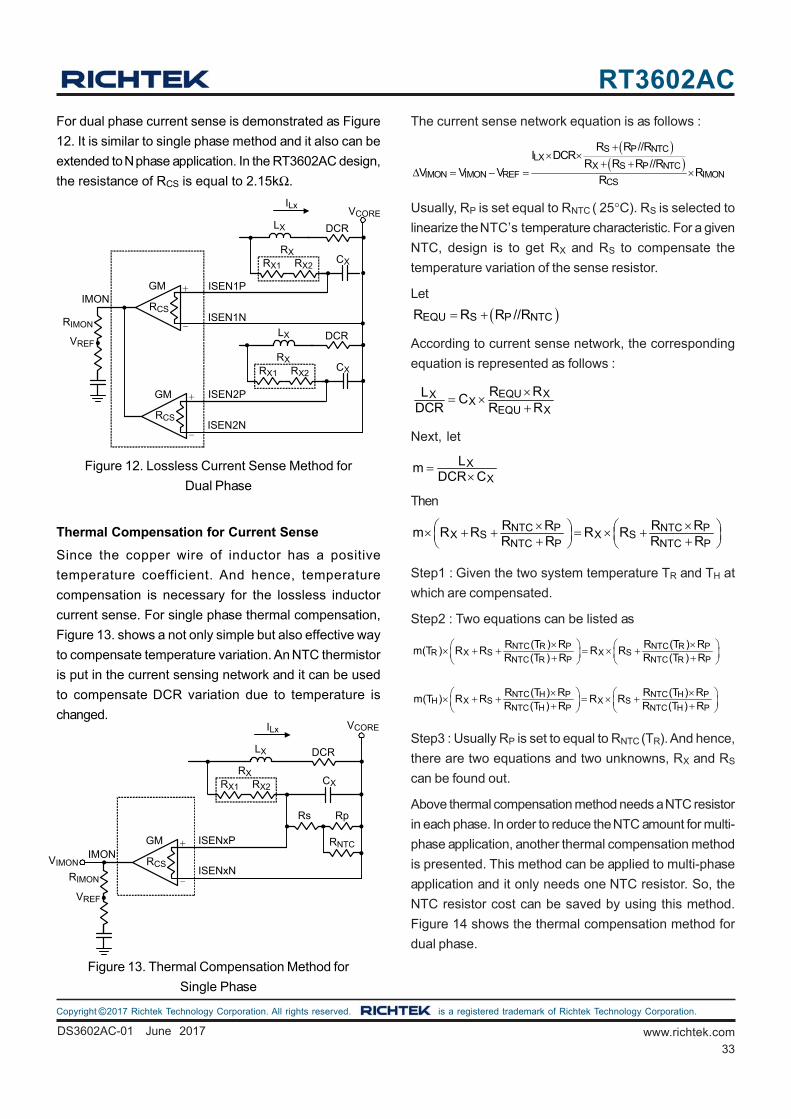
For dual phase current sense is demonstrated as Figure
12. It is similar to single phase method and it also can be
extended to N phase application. In the RT3602AC design,
the resistance of RCS is equal to 2.15kΩ.
Figure 12. Lossless Current Sense Method for
Dual Phase
Thermal Compensation for Current Sense
Since the copper wire of inductor has a positive
temperature coefficient. And hence, temperature
compensation is necessary for the lossless inductor
current sense. For single phase thermal compensation,
Figure 13. shows a not only simple but also effective way
to compensate temperature variation. An NTC thermistor
is put in the current sensing network and it can be used
to compensate DCR variation due to temperature is
changed.
Figure 13. Thermal Compensation Method for
Single Phase
The current sense network equation is as follows :
S P NTCLX
X S P NTCIMON IMON REF IMON
CS
R R //RI DCR
R R R //RV V V R
R
Usually, RP is set equal to RNTC ( 25°C). RS is selected to
linearize the NTC’s temperature characteristic. For a given
NTC, design is to get RX and RS to compensate the
temperature variation of the sense resistor.
Let
EQU S P NTCR R R //R
According to current sense network, the corresponding
equation is represented as follows :
EQU XXX
EQU X
R RL CDCR R R
Next, let
X
X
LmDCR C
Then
NTC P NTC PX S X S
NTC P NTC P
R R R Rm R R R RR R R R
Step1 : Given the two system temperature TR and TH at
which are compensated.
Step2 : Two equations can be listed as
NTC R P NTC R PR X S X S
NTC R P NTC R P
R (T ) R R (T ) Rm(T ) R R R R
R (T ) R R (T ) R
NTC H P NTC H PH X S X S
NTC H P NTC H P
R (T ) R R (T ) Rm(T ) R R R R
R (T ) R R (T ) R
Step3 : Usually RP is set to equal to RNTC (TR). And hence,
there are two equations and two unknowns, RX and RS
can be found out.
Above thermal compensation method needs a NTC resistor
in each phase. In order to reduce the NTC amount for multi-
phase application, another thermal compensation method
is presented. This method can be applied to multi-phase
application and it only needs one NTC resistor. So, the
NTC resistor cost can be saved by using this method.
Figure 14 shows the thermal compensation method for
dual phase.
ISEN1P
ISEN1N
LX DCR
CX
VCOREILx
IMON
RIMON
VREF
ISEN2P
ISEN2N
LX DCR
CX
+
-
RCS
GM
+
-
RCS
GM
RX1 RX2
RX
RX1 RX2
RX
ISENxP
ISENxN
LX DCR
CX
VCOREILx
IMON
RIMON
VREF
Rs Rp
RNTC
VIMON
+
-
RCS
GM
RX1 RX2
RX
34
RT3602AC
www.richtek.com DS3602AC-01 June 2017
©Copyright 2017 Richtek Technology Corporation. All rights reserved. is a registered trademark of Richtek Technology Corporation.
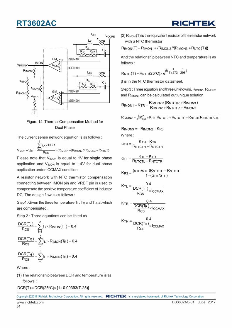
Figure 14. Thermal Compensation Method for
Dual Phase
The current sense network equation is as follows :
{
2
LX
X 1IMON ref IMON1 IMON2 IMON3 NTC
CS
I DCR
V V R [R //(R R )]}R
Please note that VIMON is equal to 1V for single phase
application and VIMON is equal to 1.4V for dual phase
application under ICCMAX condition.
A resistor network with NTC thermistor compensation
connecting between IMON pin and VREF pin is used to
compensate the positive temperature coefficient of inductor
DC. The design flow is as follows :
Step1: Given the three temperature TL, TR and TH, at which
are compensated.
Step 2 : Three equations can be listed as
2L
Li IMON LCS
i 1
DCR(T )I R (T ) 0.4
R
2
RLi IMON R
CSi 1
DCR(T )I R (T ) 0.4
R
2
HLi IMON H
CSi 1
DCR(T )I R (T ) 0.4
R
Where :
(1) The relationship between DCR and temperature is as
follows :
DCR(T) DCR(25 C) [1 0.00393(T-25)]
(2) RIMON (T) is the equivalent resistor of the resistor network
with a NTC thermistor
IMON IMON1 IMON2 IMON3 NTCR (T) R {R //[R R (T)]}
And the relationship between NTC and temperature is as
follows :
1 1β( )T 273 298NTC NTCR (T) R (25 C) e
β is in the NTC thermistor datasheet.
Step 3 : Three equation and three unknowns, RIMON1, RIMON2
and RIMON3 can be calculated out unique solution.
IMON2 NTCTR IMON3IMON1 TR
IMON2 NTCTR IMON3
R (R R )R K
R R R
2IMON2 R3 NTCTL NTCTR NTCTL NTCTR TLR3R [K K (R R ) R R ]α
IMON3 IMON2 R3R R K
Where :
TH TRTH
NTCTH NTCTR
K KαR R
TL TRTL
NTCTL NTCTR
K KαR R
TH TL NTCTH NTCTLR3
TH TL
(α /α )R RK
1 (α /α )
TLL
CCMAXCS
0.4KDCR(T )
IR
TRR
CCMAXCS
0.4KDCR(T )
IR
THH
CCMAXCS
0.4KDCR(T )
IR
ISEN1P
ISEN1N
LX DCR
CX
VCOREILx1
IMON
RIMON1
VREF
ISEN2P
ISEN2N
LX2 DCR
CX
VIMON
RIMON2
RIMON3
RNTC
+
-
RCS
GM
+
-
RCS
GM
RX1 RX2
RX
RX1 RX2
RX
35
RT3602AC
DS3602AC-01 June 2017 www.richtek.com
©Copyright 2017 Richtek Technology Corporation. All rights reserved. is a registered trademark of Richtek Technology Corporation.
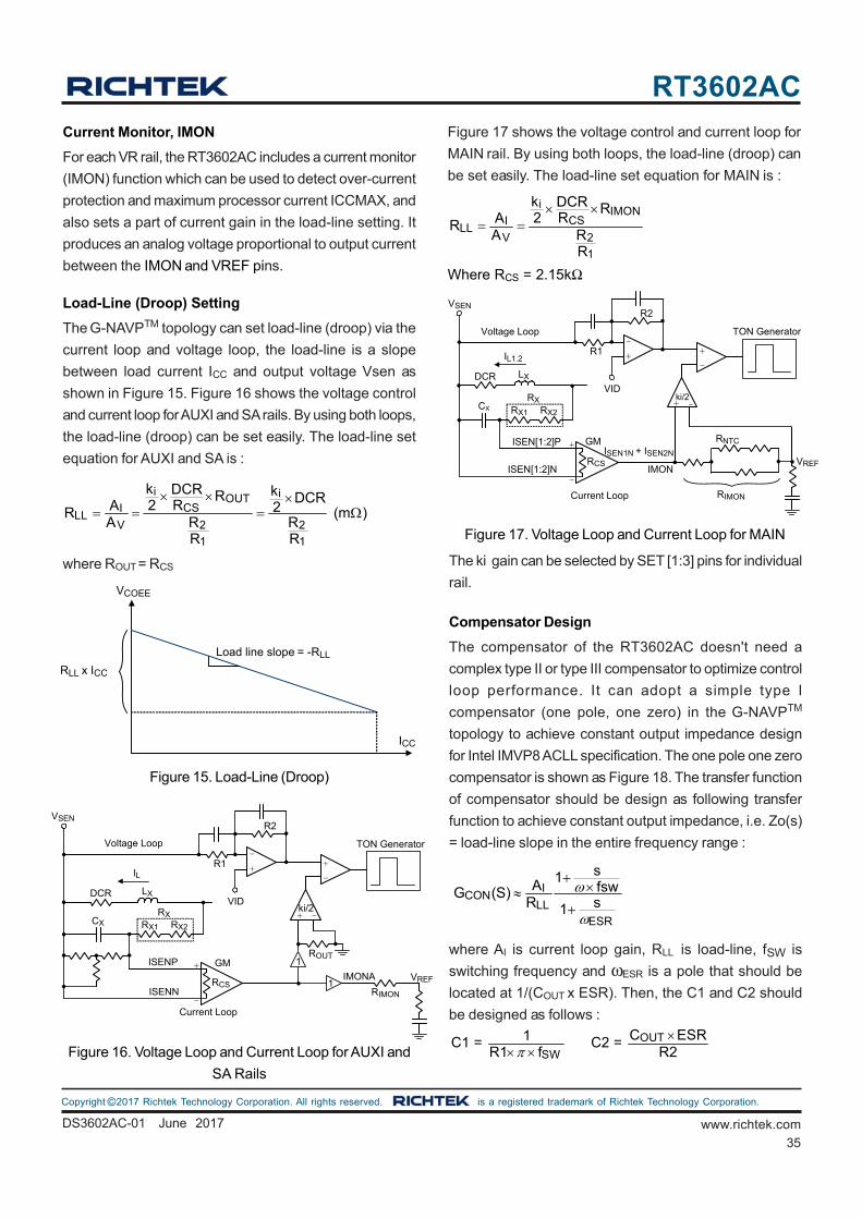
Current Monitor, IMON
For each VR rail, the RT3602AC includes a current monitor
(IMON) function which can be used to detect over-current
protection and maximum processor current ICCMAX, and
also sets a part of current gain in the load-line setting. It
produces an analog voltage proportional to output current
between the IMON and VREF pins.
Load-Line (Droop) Setting
The G-NAVPTM topology can set load-line (droop) via the
current loop and voltage loop, the load-line is a slope
between load current ICC and output voltage Vsen as
shown in Figure 15. Figure 16 shows the voltage control
and current loop for AUXI and SA rails. By using both loops,
the load-line (droop) can be set easily. The load-line set
equation for AUXI and SA is :
i iOUTCSI
LLV 2 2
1 1
k DCR kR DCR2 RA 2R (m )A R R
R R
where ROUT = RCS
ICC
VCOEE
Load line slope = -RLL
RLL x ICC
Figure 15. Load-Line (Droop)
Figure 16. Voltage Loop and Current Loop for AUXI and
SA Rails
Figure 17 shows the voltage control and current loop for
MAIN rail. By using both loops, the load-line (droop) can
be set easily. The load-line set equation for MAIN is :
iIMON
CSILL
V 2
1
k DCR R2 RAR
A RR
Where RCS = 2.15kΩ
Figure 17. Voltage Loop and Current Loop for MAIN
The ki gain can be selected by SET [1:3] pins for individual
rail.
Compensator Design
The compensator of the RT3602AC doesn't need a
complex type II or type III compensator to optimize control
loop performance. It can adopt a simple type I
compensator (one pole, one zero) in the G-NAVPTM
topology to achieve constant output impedance design
for Intel IMVP8 ACLL specification. The one pole one zero
compensator is shown as Figure 18. The transfer function
of compensator should be design as following transfer
function to achieve constant output impedance, i.e. Zo(s)
= load-line slope in the entire frequency range :
ICON
LLESR
s1A fswG (S)R s1
where AI is current loop gain, RLL is load-line, fSW is
switching frequency and ωESR is a pole that should be
located at 1/(COUT x ESR). Then, the C1 and C2 should
be designed as follows :
OUT
SW
C ESR1C1 = C2 = R1 f R2
+
-
R2
R1
VID
CX
LXDCR
IL
ISENN
ISENP
+ -ki/2
+
-
Voltage Loop TON Generator
IMONA
ROUT
VREF
VSEN
RIMON
Current Loop
1
1
+
-
RCS
GM
RX1 RX2
RX
+
-
R2
R1
VID
CX
LXDCR
IL1.2
ISEN[1:2]N
ISEN[1:2]PISEN1N + ISEN2N
+ -ki/2
+
-
Voltage Loop TON Generator
RIMON
IMON
RNTC
VREF
VSEN
Current Loop
+
-
RCS
GM
RX1 RX2
RX
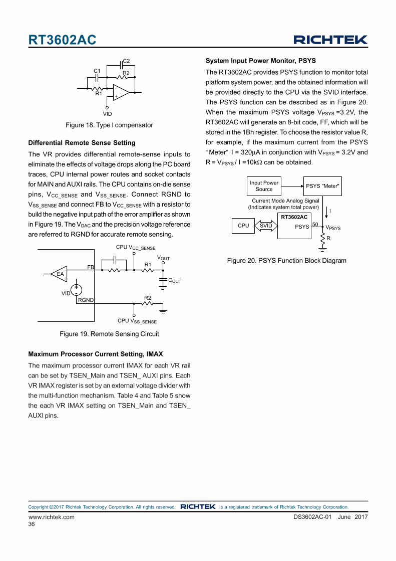
36
RT3602AC
www.richtek.com DS3602AC-01 June 2017
©Copyright 2017 Richtek Technology Corporation. All rights reserved. is a registered trademark of Richtek Technology Corporation.
Figure 18. Type I compensator
+
-
R2
R1
VID
C2
C1
Differential Remote Sense Setting
The VR provides differential remote-sense inputs to
eliminate the effects of voltage drops along the PC board
traces, CPU internal power routes and socket contacts
for MAIN and AUXI rails. The CPU contains on-die sense
pins, VCC_SENSE and VSS_SENSE. Connect RGND to
VSS_SENSE and connect FB to VCC_SENSE with a resistor to
build the negative input path of the error amplifier as shown
in Figure 19. The VDAC and the precision voltage reference
are referred to RGND for accurate remote sensing.
Figure 19. Remote Sensing Circuit
CPU VCC_SENSE
-
+
FB
RGND
EA-+
VID
R1
CPU VSS_SENSE
R2
VOUT
COUT
Maximum Processor Current Setting, IMAX
The maximum processor current IMAX for each VR rail
can be set by TSEN_Main and TSEN_ AUXI pins. Each
VR IMAX register is set by an external voltage divider with
the multi-function mechanism. Table 4 and Table 5 show
the each VR IMAX setting on TSEN_Main and TSEN_
AUXI pins.
System Input Power Monitor, PSYS
The RT3602AC provides PSYS function to monitor total
platform system power, and the obtained information will
be provided directly to the CPU via the SVID interface.
The PSYS function can be described as in Figure 20.
When the maximum PSYS voltage VPSYS =3.2V, the
RT3602AC will generate an 8-bit code, FF, which will be
stored in the 1Bh register. To choose the resistor value R,
for example, if the maximum current from the PSYS
“Meter” I = 320μA in conjunction with VPSYS = 3.2V and
R = VPSYS
/ I =10kΩ can be obtained.
Figure 20. PSYS Function Block Diagram
Input Power Source
PSYS "Meter"
RT3602AC
PSYSCPU
I
SVID 50
R
Current Mode Analog Signal(Indicates system total power)
VPSYS
37
RT3602AC
DS3602AC-01 June 2017 www.richtek.com
©Copyright 2017 Richtek Technology Corporation. All rights reserved. is a registered trademark of Richtek Technology Corporation.
Table 4. TSEN_AUXI Setting for IMAX_MAIN and zero load-line
TSEN_AUXI REFR1 R2
V = VR1+R2
ICCMAX_MAIN (A)
SA_0LL
Min Typical Max Unit 1-Phase 1-Phase POCP
2-Phase 2-Phase POCP
49.5484 50.0489 50.5494 mV 16 48 29 43.5
Disable
148.645 150.147 151.648 mV Enable
247.742 250.244 252.747 mV 18 54 33 49.5
Disable
346.839 350.342 353.846 mV Enable
445.935 450.44 454.944 mV 20 60 37 55.5
Disable
545.032 550.538 556.043 mV Enable
644.129 650.635 657.142 mV 21 63 40 60
Disable
743.226 750.733 758.24 mV Enable
842.323 850.831 859.339 mV 22 66 44 66
Disable
941.419 950.929 960.438 mV Enable
1040.52 1051.03 1061.54 mV 23 69 46 69
Disable
1139.61 1151.12 1162.64 mV Enable
1238.71 1251.22 1263.73 mV 24 72 48 72
Disable
1337.81 1351.32 1364.83 mV Enable
1436.9 1451.42 1465.93 mV 25 75 49 73.5
Disable
1536 1551.52 1567.03 mV Enable
1635.1 1651.61 1668.13 mV 26 52 50 50
Disable
1734.19 1751.71 1769.23 mV Enable
1833.29 1851.81 1870.33 mV 27 54 52 52
Disable
1932.39 1951.91 1971.43 mV Enable
2031.48 2052 2072.52 mV 28 56 53 53
Disable
2130.58 2152.1 2173.62 mV Enable
2229.68 2252.2 2274.72 mV 29 58 55 55
Disable
2328.77 2352.3 2375.82 mV Enable
2427.87 2452.39 2476.92 mV 30 60 57 57
Disable
2526.97 2552.49 2578.02 mV Enable
2626.06 2652.59 2679.12 mV 31 62 59 59
Disable
2725.16 2752.69 2780.22 mV Enable
2824.26 2852.79 2881.31 mV 33 66 61 61
Disable
2923.35 2952.88 2982.41 mV Enable
3022.45 3052.98 3083.51 mV 35 70 64 64
Disable
3121.55 3153.08 3184.61 mV Enable
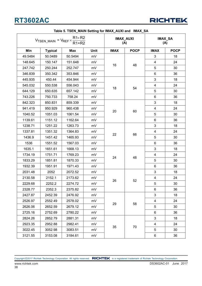
38
RT3602AC
www.richtek.com DS3602AC-01 June 2017
©Copyright 2017 Richtek Technology Corporation. All rights reserved. is a registered trademark of Richtek Technology Corporation.
Table 5. TSEN_MAIN Setting for IMAX_AUXI and IMAX_SA
TSEN_MAIN REFR1 R2
V = VR1+R2
IMAX_AUXI (A)
IMAX_SA (A)
Min Typical Max Unit IMAX POCP IMAX POCP
49.5484 50.0489 50.5494 mV
16 48
3 18
148.645 150.147 151.648 mV 4 24
247.742 250.244 252.747 mV 5 30
346.839 350.342 353.846 mV 6 36
445.935 450.44 454.944 mV
18 54
3 18
545.032 550.538 556.043 mV 4 24
644.129 650.635 657.142 mV 5 30
743.226 750.733 758.24 mV 6 36
842.323 850.831 859.339 mV
20 60
3 18
941.419 950.929 960.438 mV 4 24
1040.52 1051.03 1061.54 mV 5 30
1139.61 1151.12 1162.64 mV 6 36
1238.71 1251.22 1263.73 mV
22 66
3 18
1337.81 1351.32 1364.83 mV 4 24
1436.9 1451.42 1465.93 mV 5 30
1536 1551.52 1567.03 mV 6 36
1635.1 1651.61 1668.13 mV
24 48
3 18
1734.19 1751.71 1769.23 mV 4 24
1833.29 1851.81 1870.33 mV 5 30
1932.39 1951.91 1971.43 mV 6 36
2031.48 2052 2072.52 mV
26 52
3 18
2130.58 2152.1 2173.62 mV 4 24
2229.68 2252.2 2274.72 mV 5 30
2328.77 2352.3 2375.82 mV 6 36
2427.87 2452.39 2476.92 mV
29 58
3 18
2526.97 2552.49 2578.02 mV 4 24
2626.06 2652.59 2679.12 mV 5 30
2725.16 2752.69 2780.22 mV 6 36
2824.26 2852.79 2881.31 mV
35 70
3 18
2923.35 2952.88 2982.41 mV 4 24
3022.45 3052.98 3083.51 mV 5 30
3121.55 3153.08 3184.61 mV 6 36
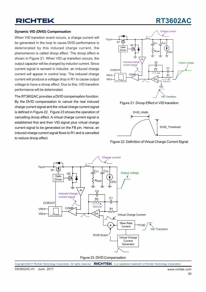
39
RT3602AC
DS3602AC-01 June 2017 www.richtek.com
©Copyright 2017 Richtek Technology Corporation. All rights reserved. is a registered trademark of Richtek Technology Corporation.
Dynamic VID (DVID) Compensation
When VID transition event occurs, a charge current will
be generated in the loop to cause DVID performance is
deteriorated by this induced charge current, the
phenomenon is called droop effect. The droop effect is
shown in Figure 21. When VID up transition occurs, the
output capacitor will be charged by inductor current. Since
current signal is sensed in inductor, an induced charge
current will appear in control loop. The induced charge
current will produce a voltage drop in R1 to cause output
voltage to have a droop effect. Due to this, VID transition
performance will be deteriorated.
The RT3602AC provides a DVID compensation function.
By the DVID compensation to cancel the real induced
charge current signal and the virtual charge current signal
is defined in Figure 22. Figure 23 shows the operation of
cancelling droop effect. A virtual charge current signal is
established first and then VID signal plus virtual charge
current signal to be generated on the FB pin. Hence, an
induced charge current signal flows to R1 and is cancelled
to reduce droop effect.Figure 22. Definition of Virtual Charge Current Signal
DVID_Threshold
DVID_Width
VIN
Gate Driver
Q1Q2
L
RESR
CO2
CPU
C2
Charge current
Induced charge current signal
CO1
Ai
R1
R2 C1
+
-EA+
-COMP
CCRCOT
tON
VID Transition
IDROOP
VID
Output voltage
VIN
VID Virtual Charge Current
Slew Rate Control
Virtual Charge Current
Generator
+
DVID Event
Figure 23. DVID Compensation
Figure 21. Droop Effect in VID transition
VIN
Gate Driver
Q1Q2
L
RESR
CO2
CPU
C2
Charge current
Induced charge current signal
CO1
Ai
R1
R2 C1
+
-EA+
-COMP
CCRCOT
tON
VID Transition
IDROOP
VID
Output voltage
VIN
VID
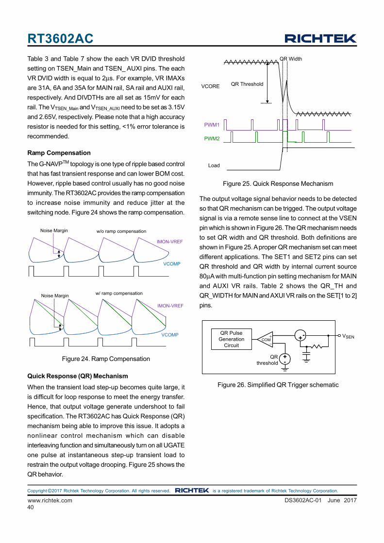
40
RT3602AC
www.richtek.com DS3602AC-01 June 2017
©Copyright 2017 Richtek Technology Corporation. All rights reserved. is a registered trademark of Richtek Technology Corporation.
Quick Response (QR) Mechanism
When the transient load step-up becomes quite large, it
is difficult for loop response to meet the energy transfer.
Hence, that output voltage generate undershoot to fail
specification. The RT3602AC has Quick Response (QR)
mechanism being able to improve this issue. It adopts a
nonlinear control mechanism which can disable
interleaving function and simultaneously turn on all UGATE
one pulse at instantaneous step-up transient load to
restrain the output voltage drooping. Figure 25 shows the
QR behavior.
The output voltage signal behavior needs to be detected
so that QR mechanism can be trigged. The output voltage
signal is via a remote sense line to connect at the VSEN
pin which is shown in Figure 26. The QR mechanism needs
to set QR width and QR threshold. Both definitions are
shown in Figure 25. A proper QR mechanism set can meet
different applications. The SET1 and SET2 pins can set
QR threshold and QR width by internal current source
80μA with multi-function pin setting mechanism for MAIN
and AUXI VR rails. Table 2 shows the QR_TH and
QR_WIDTH for MAIN and AXUI VR rails on the SET[1 to 2]
pins.
Table 3 and Table 7 show the each VR DVID threshold
setting on TSEN_Main and TSEN_ AUXI pins. The each
VR DVID width is equal to 2μs. For example, VR IMAXs
are 31A, 6A and 35A for MAIN rail, SA rail and AUXI rail,
respectively. And DIVDTHs are all set as 15mV for each
rail. The VTSEN_Main and VTSEN_AUXI need to be set as 3.15V
and 2.65V, respectively. Please note that a high accuracy
resistor is needed for this setting, <1% error tolerance is
recommended.
Ramp Compensation
The G-NAVPTM topology is one type of ripple based control
that has fast transient response and can lower BOM cost.
However, ripple based control usually has no good noise
immunity. The RT3602AC provides the ramp compensation
to increase noise immunity and reduce jitter at the
switching node. Figure 24 shows the ramp compensation.
Noise Margin
VCOMP
Noise Margin
IMON-VREF
w/o ramp compensation
w/ ramp compensation
IMON-VREF
VCOMP
Figure 24. Ramp Compensation
Figure 25. Quick Response Mechanism
QR Threshold
QR Width
PWM1
PWM2
VCORE
Load
Figure 26. Simplified QR Trigger schematic
VSENQR Pulse
GenerationCircuit
COM+
-
+-
QR threshold
+-
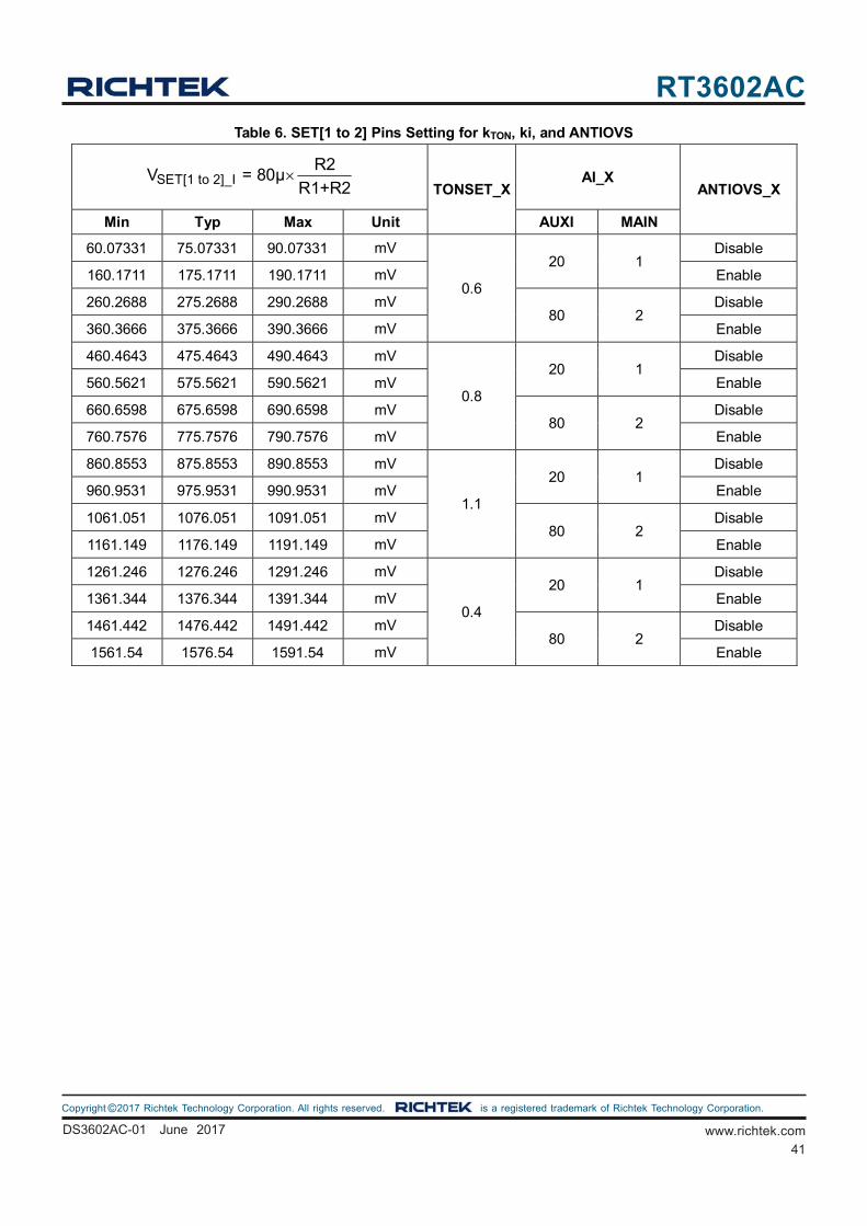
41
RT3602AC
DS3602AC-01 June 2017 www.richtek.com
©Copyright 2017 Richtek Technology Corporation. All rights reserved. is a registered trademark of Richtek Technology Corporation.
Table 6. SET[1 to 2] Pins Setting for kTON, ki, and ANTIOVS
SET[1 to 2]_IR2
V = 80μR1+R2
TONSET_X
AI_X ANTIOVS_X
Min Typ Max Unit AUXI MAIN
60.07331 75.07331 90.07331 mV
0.6
20 1 Disable
160.1711 175.1711 190.1711 mV Enable
260.2688 275.2688 290.2688 mV 80 2
Disable
360.3666 375.3666 390.3666 mV Enable
460.4643 475.4643 490.4643 mV
0.8
20 1 Disable
560.5621 575.5621 590.5621 mV Enable
660.6598 675.6598 690.6598 mV 80 2
Disable
760.7576 775.7576 790.7576 mV Enable
860.8553 875.8553 890.8553 mV
1.1
20 1 Disable
960.9531 975.9531 990.9531 mV Enable
1061.051 1076.051 1091.051 mV 80 2
Disable
1161.149 1176.149 1191.149 mV Enable
1261.246 1276.246 1291.246 mV
0.4
20 1 Disable
1361.344 1376.344 1391.344 mV Enable
1461.442 1476.442 1491.442 mV 80 2
Disable
1561.54 1576.54 1591.54 mV Enable
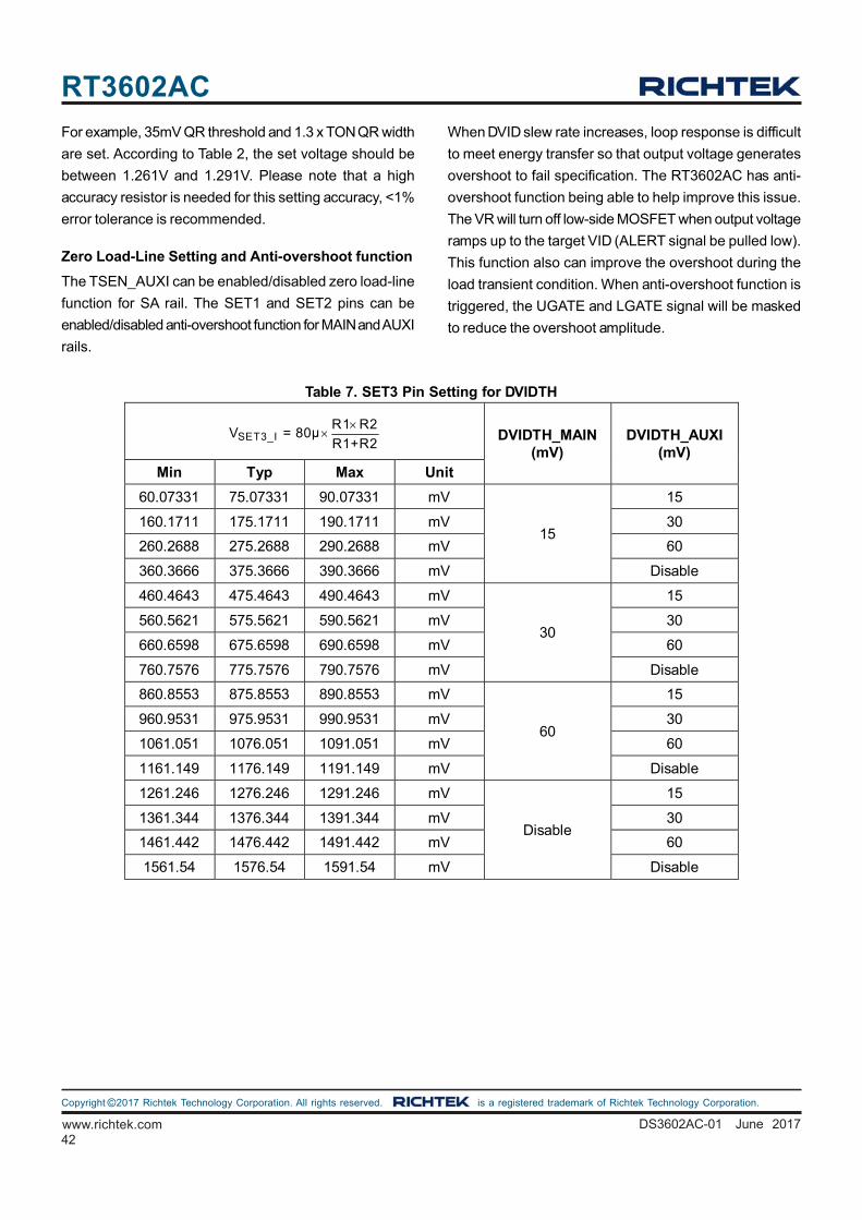
42
RT3602AC
www.richtek.com DS3602AC-01 June 2017
©Copyright 2017 Richtek Technology Corporation. All rights reserved. is a registered trademark of Richtek Technology Corporation.
For example, 35mV QR threshold and 1.3 x TON QR width
are set. According to Table 2, the set voltage should be
between 1.261V and 1.291V. Please note that a high
accuracy resistor is needed for this setting accuracy, <1%
error tolerance is recommended.
Zero Load-Line Setting and Anti-overshoot function
The TSEN_AUXI can be enabled/disabled zero load-line
function for SA rail. The SET1 and SET2 pins can be
enabled/disabled anti-overshoot function for MAIN and AUXI
rails.
When DVID slew rate increases, loop response is difficult
to meet energy transfer so that output voltage generates
overshoot to fail specification. The RT3602AC has anti-
overshoot function being able to help improve this issue.
The VR will turn off low-side MOSFET when output voltage
ramps up to the target VID (ALERT signal be pulled low).
This function also can improve the overshoot during the
load transient condition. When anti-overshoot function is
triggered, the UGATE and LGATE signal will be masked
to reduce the overshoot amplitude.
Table 7. SET3 Pin Setting for DVIDTH
SET3_IR1 R2
V = 80μR1+R2
DVIDTH_MAIN
(mV) DVIDTH_AUXI
(mV) Min Typ Max Unit
60.07331 75.07331 90.07331 mV
15
15
160.1711 175.1711 190.1711 mV 30
260.2688 275.2688 290.2688 mV 60
360.3666 375.3666 390.3666 mV Disable
460.4643 475.4643 490.4643 mV
30
15
560.5621 575.5621 590.5621 mV 30
660.6598 675.6598 690.6598 mV 60
760.7576 775.7576 790.7576 mV Disable
860.8553 875.8553 890.8553 mV
60
15
960.9531 975.9531 990.9531 mV 30
1061.051 1076.051 1091.051 mV 60
1161.149 1176.149 1191.149 mV Disable
1261.246 1276.246 1291.246 mV
Disable
15
1361.344 1376.344 1391.344 mV 30
1461.442 1476.442 1491.442 mV 60
1561.54 1576.54 1591.54 mV Disable
43
RT3602AC
DS3602AC-01 June 2017 www.richtek.com
©Copyright 2017 Richtek Technology Corporation. All rights reserved. is a registered trademark of Richtek Technology Corporation.
VAUXI Specification
Input Voltage 19V
No. of Phase 1
Normal VID 1.35V
ICCMAX 35
ICC-Dyn 28
Load-Line 2.1m
Fast Slew Rate 37.5mV/s
MAX Switching Frequency 700kHz
The output filter requirements of VRTB specification are
as follows :
Output Inductor : 220nH/0.875mΩ
Output Ceramic Capacitor: 47μF (6pcs)
Output Ceramic Capacitor:10μF (9pcs)
Loop Design :
On time setting: Using the specification, then can get
that TON is 108ns.
The kTON parameter can be calculated after the on-time
is decided.
DACON
TON IN DAC
1.2μ VT 15n
k (V V )
Choosing the nearest on-time setting kTON = 1.1
Over-Current Protection
The RT3602AC has dual OCP mechanism. One is named
SUM-OCP, the other is called SPIKE-OCP. The over current
protection (OCP) forces high-side MOSFET and low-side
MOSFET off by shutting down internal PWM logic drivers.
The RT3602AC provides SUM-OCP which is 160% of
IMON_04. IMON_04 is the current that makes (VIMON −VREF ) = 0.4V. When output current is higher than the
SUM-OCP threshold, SUM-OCP is latched with a 40μs
delay time to prevent false trigger. Besides, the SUM-
OCP function is masked when dynamic VID transient
occurs and after dynamic VID transition, SUM-OCP is
masked for 80μs. The other one is SPIKE-OCP which
should trip when the output current exceeds SPIKE_OCP
threshold during first DVID. SPIKE_OCP threshold is
dependent on IMAX level as shown in Table 4 and Table 5.
When output current is higher than the SPIKE-OCP
threshold, SPIKE-OCP is latched with a 1μs delay time
to prevent false trigger.
Output Over-Voltage Protection
An OVP condition is detected when the VSEN pin is
350mV more than VID. When OVP is detected, the high-
side gate voltage UGATEx is pulled low and the low-side
gate voltage LGATEx is pulled high. OVP is latched with
a 0.5μs delay- to prevent false trigger.
Negative Voltage Protection
Since the OVP latch continuously turns on all low-side
MOSFETs of the VR, the VR will suffer negative output
voltage. When the VSEN detects a voltage below −0.07V
after triggering OVP, the VR triggers NVP to turn off all
low-side MOSFETs of the VR while the high-side
MOSFETs remain off. After triggering NVP, if the output
voltage rises above 0V, the OVP latch restarts to turn on
all low-side MOSFETs. Therefore, the output voltage may
bounce between 0V and −0.07V due to OVP latch and
NVP triggering. The NVP function will be active only after
OVP is triggered.
Under-Voltage Protection
When the VSEN pin voltage is 350mV less than VID, UVP
will be latched. When UVP latched, the both UGATEx
and LGATEx are pulled low. A 3μs delay is used in UVP
detection circuit to prevent false trigger. Besides, the UVP
function is masked when dynamic VID transient occurs
and after dynamic VID transition, UVP is masked for 80μs.
Design Step :
The RT3602AC Excel based design tool is available. Users
can contact your Richtek representative to get the
spreadsheet. Three main design procedures of the
RT3602AC design, first step is loop design, second step
is pin setting design, and the last step is protection
settings. The following design example is to explain the
RT3602AC design procedure :
AUXI VR
44
RT3602AC
www.richtek.com DS3602AC-01 June 2017
©Copyright 2017 Richtek Technology Corporation. All rights reserved. is a registered trademark of Richtek Technology Corporation.
SA VR
VSA Specification
Input Voltage 19V
No. of Phase 1
Normal VID 1.05V
ICCMAX 6
ICC-Dyn 3
Load-Line 10.3m
Fast Slew Rate 37.5mV/s
MAX Switching Frequency 800kHz
The output filter requirements of VRTB specification are
as follows :
Output Inductor: 820nH/6.7mΩ
Output Ceramic Capacitor: 47μF (4pcs)
Output Ceramic Capacitor:10μF (8pcs)
Loop Design :
On time setting : Using the specification, then can get
that TON is 96ns.
The kTON parameter can be calculated after the on-time
is decided.
DACON
TON IN DAC
1.2μ VT 15n
k (V V )
Choosing the nearest on-time setting kTON = 1.1
Current sensor adopts lossless RC filter to sense current
signal in DCR. For getting an expected load transient
waveform RXCX time constant needs to match LX/DCRX.
CX = 0.47μF, RNTC = 4.7kΩ and Rp = 4.7kΩ are set,
then
EQU S P NTCR R R //R
EQU XXX
EQU X
R RL CDCR R R
By using the design tool, RS and RX can be determined,
are equal to 165Ω and 280Ω, respectively.
IMON resistor network design :
IMONIMON
EQU
X EQU
∆V 2.15kR 23.79kRICCMAX DCR
R R
Current sensor adopts lossless RC filter to sense current
signal in DCR. For getting an expected load transient
waveform RXCX time constant needs to match LX/DCRX.
CX = 0.47μF, RNTC = 10kΩ and RP = 10kΩ are set, then
EQU S P NTCR R R //R
EQU XXX
EQU X
R RL CDCR R R
By using the design tool, RS and RX can be determined,
are equal to 220Ω and 590Ω, respectively.
IMON resistor network design :
IMONIMON
EQU
X EQU
∆V 2.15kR 31.25kRICCMAX DCR
R R
Load-line design : 2.1mΩ droop is requirement, because
DCR and ki are decided to 0.875mΩ and 20,
respectively. The voltage loop Av gain is also can be
determined by following equation :
iI
LLV 2
1
k DCRA 2RA R
R
R1 = 10kΩ is usually decided and here R2 is chosen to
37.4kΩ.
Typical compensator design can use the following
equations to design C1 and C2 values
11 SW
1C 45.5pFR π F
OUT2
2
C ESRC 33pFR
For Intel platform, in order to induce the band width to
enhance transient performance to meet Intel's criterion,
the zero location can be designed close to 1/10 of the
switching frequency or less than the 1/10 of switching
frequency.
45
RT3602AC
DS3602AC-01 June 2017 www.richtek.com
©Copyright 2017 Richtek Technology Corporation. All rights reserved. is a registered trademark of Richtek Technology Corporation.
VMAIN Specification
Input Voltage 19V
No. of Phase 1
Normal VID 1.35V
ICCMAX 31
ICC-Dyn 28
Load-Line 3.1m
Fast Slew Rate 37.5mV/s
MAX Switching Frequency 700kHz
The output filter requirements of VRTB specification are
as follows :
Output Inductor: 220nH/0.875mΩ
Output Bulk Capacitor: 330μF/2V.4.5mΩ (1pcs)
Output Ceramic Capacitor: 47μF (6pcs)
Output Ceramic Capacitor: 22μF (7pcs)
Output Ceramic Capacitor:10μF (2pcs)
Load-line design : 10.3mΩ droop is requirement,
because DCR and ki are decided to 6.7mΩ and 20,
respectively. The voltage loop Av gain is also can be
determined by following equation :
iI
LLV 2
1
k DCRA 2RA R
R
R1 = 10kΩ is usually decided and here R2 is chosen to
58.5kΩ.
Typical compensator design can use the following
equations to design C1 and C2 values
11 SW
1C 45.5pFR π F
OUT2
2
C ESRC 56pFR
For Intel platform, in order to induce the band width to
enhance transient performance to meet Intel's criterion,
the zero location can be designed close to 1/10 of the
switching frequency or less than the 1/10 of switching
frequency.
MAIN VR
Loop Design :
On time setting: Using the specification, then can get
that TON parameter can be calculated after the on-time
is decided.
DACON
TON IN DAC
1.2μ VT 15n
k (V V )
Choosing the nearest on-time setting kTON = 1.1
Current sensor adopts lossless RC filter to sense current
signal in DCR. For getting an expected load transient
waveform RXCX time constant needs to match LX/DCRX.
CX = 0.47μF is set, then
XX
X
LR 5301μF DCR
IMON resistor network design : TL = 25°C, TR = 50°Cand TH = 100oC are decided, NTC thermistor = 100kΩ@ 25oC, β = 4485 and ICCMAX = 31A. RIMON1 =
16.74kΩ, RIMON2 = 17.35kΩ and RIMON3 = 9.16kΩ can
be decided. The REQ (25°C) = 31.78kΩ.
Load-line design: 3.1mΩ droop is requirement, because
DCR and ki are decided to 0.875mΩ and 2, respectively.
The voltage loop Av gain is also can be determined by
following equation :
iIMON
CSILL
V 2
1
k DCR R2 RAR
A RR
R1 = 10kΩ is usually decided and here R2 is chosen to
42.2kΩ.
Typical compensator design can use the following
equations to design C1 and C2 values
11 SW
1C 45.5pFR π F
OUT2
2
C ESRC 55pFR
For intel platform, in order to induce the band width to
enhance transient performance to meet intel's criterion,
the zero location can be designed close to 1/10 of the
switching frequency or less than the 1/10 of switching
frequency.
46
RT3602AC
www.richtek.com DS3602AC-01 June 2017
©Copyright 2017 Richtek Technology Corporation. All rights reserved. is a registered trademark of Richtek Technology Corporation.
Pin Setting Design :
SET1 resistor network design: From above designs,
parameters of kTON_AUXI and ki_AUXI are 1.1 and 20,
respectively. The AUXI_QR_TH is set to disable and
AUXI_QR_Width is designed as 0.7 x TON. And anti-
overshoot function is disabled for MAIN rail. By using
the information, the two equation can be listed by using
multi-function pin setting mechanism :
2
1 2
R3.2 175.17mVR R
1 2
1 2
R R80μ 975.9mVR R
R1 = 222.86kΩ and R2 = 12.91kΩ.
SET2 resistor network design : From above designs,
parameters of kTON_MAIN and ki_MAIN are 1.1 and 2,
respectively. The MAIN_QR_TH is set to 15mV and
MAIN_QR_Width is designed as 0.7 x TON. And anti-
overshoot function is enabled for AUXI rails. By using
the information, the two equation can be listed by using
multi-function pin setting mechanism :
2
1 2
R3.2 575.56mVR R
1 2
1 2
R R80μ 1176.14mVR R
R1 = 81.74kΩ and R2 = 17.93kΩ.
SET3 resistor network design: From above designs,
parameter of kTON_SA is 1.1. The DVID thresholds are
60mV, 15mV, and 60mV for MAIN, AUXI, and SA rail.
The force-non-zero VBOOT is setting as Intel VBOOT.
By using the information, the two equation can be listed
by using multi-function pin setting mechanism :
2
1 2
R3.2 1326.3mVR R
1 2
1 2
R R80μ 875.86mVR R
R1 = 26.4kΩ and R2 = 18.7kΩ.
TSEN_AUXI resistor network design : The ICCMAX of
MAIN rail is designed as 31A. And zero load-line function
for SA rail is disabled. By using the information, the
equation can be shown as below :
2
1 2
R3.2 2.65VR R
TSEN_MAIN resistor network design : The ICCMAXs
are designed as 35A and 6A for AUXI and SA rail. By
using the information, the equation can be listed by
using multi-function pin setting mechanism :
2
1 2
R3.2 3.15VR R
Protection Settings :
OVP/UVP protections: When the VSEN pin voltage is
350mV higher than VID, the OVP will be latched. When
the VSEN pin voltage is 350mV lower than VID, the
UVP will be latched.
TSEN and VR_HOT design : Using the following
equation to calculate related resistances for VR_HOT
setting.
TSEN 3 NTC 1 2V 80μ (R //R ) (R //R )
Choosing R1 = 100kΩ and an NTC thermistor RNTC (25°C)
= 100kΩ and its β = 4485. When temperature is 100°C,
the RNTC (100°C) = 4.85kΩ. According to TSEN pins for
multi-function mechanism, three equations can be got
as following for AUXI VR rail :
o o3 1 2TSEN_AUXI(25 C) NTC (25 C)V 80μ (R //R ) (R //R ) 1.624V
o o3 1 2TSEN_AUXI(100 C) NTC (100 C)V 80μ (R //R ) (R //R ) 1.092V
2
1 2
R3.2 2.65VR R
R1 = 8.94kΩ, R2 = 600.45kΩ and R3 = 5618.685kΩ.
Three equations can be got as following for MAIN VR rail :
o o3 1 2TSEN_MAIN(25 C) NTC(25 C)V 80μ (R //R ) (R //R ) 1.624V
o o3 1 2TSEN_MAIN(100 C) NTC(100 C)V 80μ (R //R ) (R //R ) 1.092V
2
1 2
R3.2 3.15VR R
R1 = 8.94kΩ, R2 = 63kΩ and R3 = 5618.685kΩ.
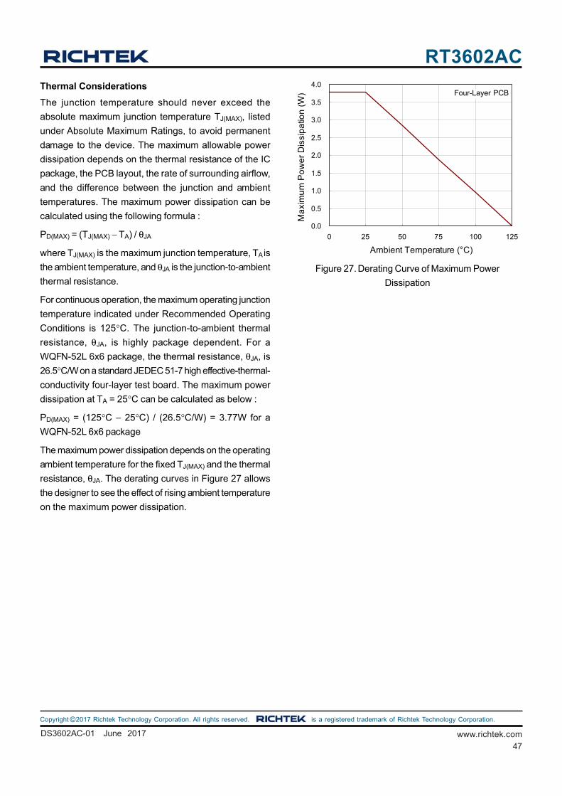
47
RT3602AC
DS3602AC-01 June 2017 www.richtek.com
©Copyright 2017 Richtek Technology Corporation. All rights reserved. is a registered trademark of Richtek Technology Corporation.
Figure 27. Derating Curve of Maximum Power
Dissipation
0.0
0.5
1.0
1.5
2.0
2.5
3.0
3.5
4.0
0 25 50 75 100 125
Ambient Temperature (°C)
Ma
xim
um
Po
we
r D
issi
pa
tion
(W
) 1 Four-Layer PCBThermal Considerations
The junction temperature should never exceed the
absolute maximum junction temperature TJ(MAX), listed
under Absolute Maximum Ratings, to avoid permanent
damage to the device. The maximum allowable power
dissipation depends on the thermal resistance of the IC
package, the PCB layout, the rate of surrounding airflow,
and the difference between the junction and ambient
temperatures. The maximum power dissipation can be
calculated using the following formula :
PD(MAX) = (TJ(MAX) − TA) / θJA
where TJ(MAX) is the maximum junction temperature, TA is
the ambient temperature, and θJA is the junction-to-ambient
thermal resistance.
For continuous operation, the maximum operating junction
temperature indicated under Recommended Operating
Conditions is 125°C. The junction-to-ambient thermal
resistance, θJA, is highly package dependent. For a
WQFN-52L 6x6 package, the thermal resistance, θJA, is
26.5°C/W on a standard JEDEC 51-7 high effective-thermal-
conductivity four-layer test board. The maximum power
dissipation at TA = 25°C can be calculated as below :
PD(MAX) = (125°C − 25°C) / (26.5°C/W) = 3.77W for a
WQFN-52L 6x6 package
The maximum power dissipation depends on the operating
ambient temperature for the fixed TJ(MAX) and the thermal
resistance, θJA. The derating curves in Figure 27 allows
the designer to see the effect of rising ambient temperature
on the maximum power dissipation.
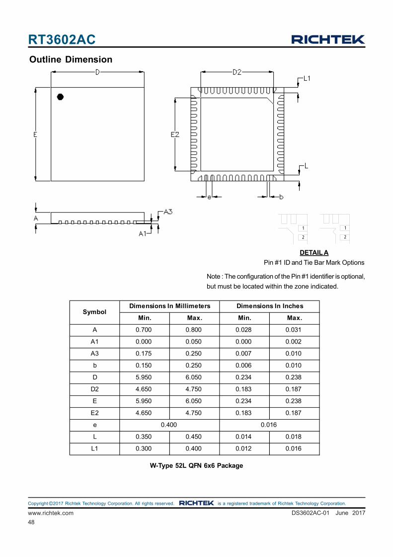
48
RT3602AC
www.richtek.com DS3602AC-01 June 2017
©Copyright 2017 Richtek Technology Corporation. All rights reserved. is a registered trademark of Richtek Technology Corporation.
Outline Dimension
W-Type 52L QFN 6x6 Package
Min. Max. Min. Max.
A 0.700 0.800 0.028 0.031
A1 0.000 0.050 0.000 0.002
A3 0.175 0.250 0.007 0.010
b 0.150 0.250 0.006 0.010
D 5.950 6.050 0.234 0.238
D2 4.650 4.750 0.183 0.187
E 5.950 6.050 0.234 0.238
E2 4.650 4.750 0.183 0.187
e
L 0.350 0.450 0.014 0.018
L1 0.300 0.400 0.012 0.016
SymbolDimensions In Millimeters Dimensions In Inches
0.400 0.016
Note : The configuration of the Pin #1 identifier is optional,
but must be located within the zone indicated.
DETAIL A
Pin #1 ID and Tie Bar Mark Options
11
2 2
49
RT3602AC
DS3602AC-01 June 2017 www.richtek.com
Richtek Technology Corporation14F, No. 8, Tai Yuen 1st Street, Chupei City
Hsinchu, Taiwan, R.O.C.
Tel: (8863)5526789
Richtek products are sold by description only. Customers should obtain the latest relevant information and data sheets before placing orders and should verify
that such information is current and complete. Richtek cannot assume responsibility for use of any circuitry other than circuitry entirely embodied in a Richtek
product. Information furnished by Richtek is believed to be accurate and reliable. However, no responsibility is assumed by Richtek or its subsidiaries for its use;
nor for any infringements of patents or other rights of third parties which may result from its use. No license is granted by implication or otherwise under any patent
or patent rights of Richtek or its subsidiaries.