Embed Size (px)
DESCRIPTION
jhgjhh
Citation preview
TIME BASED INDUSTRIAL AUTOMATION USING DALLAS RTC AND I2C
Abstract
Power Saving Using Time Operated Electrical Appliance Controlling System is a reliable
circuit that takes over the task of switch on/off the electrical devices with respect to time.
This project replaces the Manual Switching. It has an Inbuilt Real Time Clock which tracks
over the Real Time. When this time equals to the programmed time, then the corresponding
Relay for the device is switched ON. The switching time can be edited at any Time using the
keypad. The Real Time Clock is displayed on LCD display.
INTRODUCTION
1.1 THE REAL-TIME CLOCK
A real-time clock (RTC) is a computer clock (most often in the form of an integrated
circuit) that keeps track of the current time. Although the term often refers to the devices in
personal computers, servers and embedded systems, RTCs are present in almost any
electronic device which needs to keep accurate time.
A real time clock (RTC) is a timepiece module having an independent battery for
operation and has a backup RAM always supplied with electric power from the battery.
Many data processing circuits utilize real-time clocks to provide a real-time clock value
indicating, for example, the current day, date and time.
Typically, when the data processing circuit is first activated, the correct day, date and time
may need to be set. When the data processing circuit is shut down, power is maintained to the
real-time clock by a battery, so that the real-time clock may continue to operate. Personal
computers and digital electronics typically include a real time clock that tracks the time of
day, day, month, and year. The use of wireless communication systems continues to expand.
In some digital cellular systems, the in-phone real-time clock is synchronized to the
precise local time given by the base station to which the phone is communicating with
1
currently. This feature is known as automatic local time adjustment. To implement automated
and programmable functions, a real time clock within the wireless device is generally
required. The real time clock provides a precise representation of time which can be
compared to stored values in registers to provide automated functions. During power
interruptions, the real time clock is typically powered from either a dedicated clock battery,
such as a small button cell, or from a storage capacitor.
On a computer mother board, a RTC is provided to maintain the data stored in a
CMOS on the mother board. Generally, electrical power is provided to a RTC by a battery
arranged on the mother board. The RTC is used to update the current time and date within the
computer system without any intervention from the system processor. Usually the RTC and
other peripheral devices are coupled to the peripheral bus through an interrupt controller.
Such a clock has various uses such as time stamping files and inserting dates into documents.
The RTC is used to update a program clock, typically a date/time clock maintained by the
operating system (OS) and referred to herein as the OS clock. An operating system may
include a system clock to provide a system time for measuring small increments of time. The
system clock may update the system clock in response to a periodic interrupt generated by a
system timer, or a real time clock event timer.
A Real-Time-Clock (RTC) is, as the name suggests, a clock which keeps track of time
in a "real mode." While there are a number of 8051-compatible microcontrollers that have
built-in, accurate real-time clocks (especially from Dallas Semiconductor), some simple
applications may benefit from a software RTC solution that uses the built-in capabilities of an
8051 microcontroller.
1.2 BENEFITS
The purpose of using real-time clocks has the following benefits:
• Low power consumption (important when running from alternate power)
• Frees the main system for time-critical tasks
• Sometimes more accurate than other methods
2
1.3 POWER SOURCE
RTCs often have an alternate source of power, so they can continue to keep time while the
primary source of power is off or unavailable. This alternate source of power is normally a
lithium battery in older systems, but some newer systems use a supercapacitor, because they
are rechargeable and can be soldered. The alternate power source can also supply power to
battery backed RAM.
1.4 TIMING
Most RTCs use a crystal oscillator, but some use the power line frequency. In many
cases the oscillator's frequency is 32.768 kHz. This is the same frequency used in quartz
clocks and watches, and for the same reasons, namely that the frequency is exactly 215 cycles
per second, which is a convenient rate to use with simple binary counter circuits.
1.5 USAGE
A real-time clock (RTC) is a battery-powered clock that is included in a microchip in
a computer motherboard. This microchip is usually separate from the microprocessor and
other chips and is often referred to simply as "the CMOS" (complementary metal-oxide
semiconductor). A small memory on this microchip stores system description or setup values
- including current time values stored by the real-time clock. The time values are for the year,
month, date, hours, minutes, and seconds. When the computer is turned on, the Basic Input-
Output Operating System (BIOS) that is stored in the computer's read-only memory (ROM)
microchip reads the current time from the memory in the chip with the real-time clock.
Many integrated circuit manufacturers make RTCs, including Intersil, Maxim,
Philips, Texas Instruments and STMicroelectronics. The RTC was introduced to PC
compatibles by the IBM PC/AT in 1984, which used a MC146818 RTC. Later Dallas made
compatible RTCs, which was often used in older personal computers, and are easily found on
motherboards because of their distinctive black battery cap and silkscreened logo. In newer
systems the RTC is integrated into the Southbridge chip. Popular serial clock circuit is
numerous now, such as DS1302, DS1307, PCF8485, etc... The interface of the circuit is
simple, cheap, easy to use, widely adopted. The real-time clock circuit DS1302 is that one
3
kind of DALLAS Company has circuit that detailed electric current of tiny stream charges
ability, the leading particulars adopts the serial data transmission, can offer the programming
charging function for losing power of electric protection, and can close the charging function.
Structure of DS1302
DS1302 is a kind of high performance which U.S.A. DALLAS Company introduces, low
power consumption, real-time clock circuit with RAM, it can for day, month and year,
Sunday, when, go on minute or second time, have leap year to compensate the function,
working voltage is 2.5V- 5.5V. Adopt three line interfaces and CPU to carry on synchronous
communication, a clock signal or RAM datum of conveying a plurality of byte that and can
adopt burst way. There are RAM registers used for preserving the data in temporariness of
31* 8 for one within DS1302. DS1302 is the upgrading products of DS1202, compatible with
DS1202, but increased the power duplicate supply pin of the main power source /
back,offered and carried on the charged ability of detailed electric current of tiny stream to
the power of back at the same time.This is one kind of RTC that is usually used. Some
microcontrollers have a real-time clock built in, generally only the ones with many other
features and peripherals. The complete operation of the DS1307 RTC and its use in
controlling home appliances is described in the other chapters.
4
DESCRIPTION
2.1 GENERAL DESCRIPTION
The DS1307 serial real-time clock (RTC) is a low power, full binary-coded decimal
(BCD) clock/calendar plus 56 bytes of NV SRAM.
Address and data are transferred serially through an I2C, bidirectional bus. The
clock/calendar provides seconds, minutes, hours, day, date, month, and year information. The
end of the month date is automatically adjusted for months with fewer than 31 days,
including corrections for leap year. The clock operates in either the 24-hour or 12-hour
format with AM/PM indicator. The DS1307 has a built-in power-sense circuit that detects
power failures and automatically switches to the backup supply. Timekeeping operation
continues while the part operates from the backup supply.
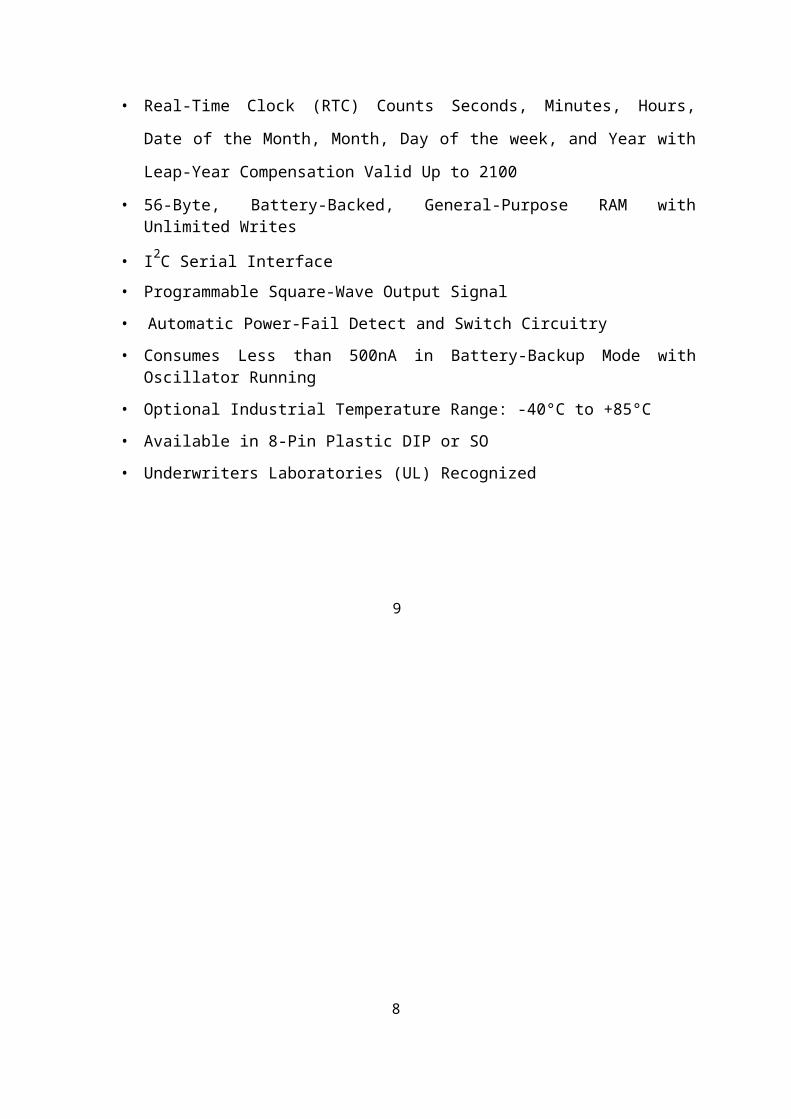
2.2 FEATURES
• Real-Time Clock (RTC) Counts Seconds, Minutes, Hours, Date of the Month, Month,
Day of the week, and Year with Leap-Year Compensation Valid Up to 2100
• 56-Byte, Battery-Backed, General-Purpose RAM with Unlimited Writes
• I2C Serial Interface
• Programmable Square-Wave Output Signal
• Automatic Power-Fail Detect and Switch Circuitry
• Consumes Less than 500nA in Battery-Backup Mode with Oscillator Running
• Optional Industrial Temperature Range: -40°C to +85°C
• Available in 8-Pin Plastic DIP or SO
• Underwriters Laboratories (UL) Recognized
9
5
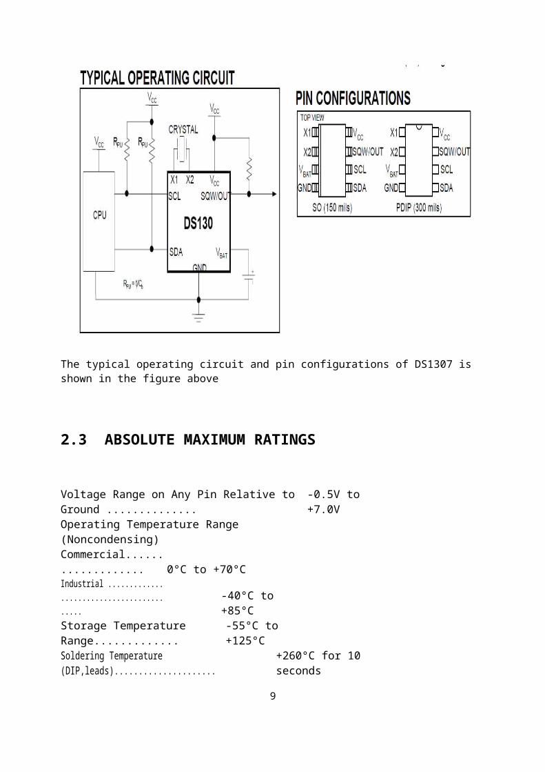
The typical operating circuit and pin configurations of DS1307 is shown in the figure above
2.3 ABSOLUTE MAXIMUM RATINGS
Voltage Range on Any Pin Relative to Ground .............. -0.5V to +7.0V
Operating Temperature Range (Noncondensing)
Commercial................... 0°C to +70°C
Industrial .......................................... -40°C to +85°C
Storage Temperature Range............. -55°C to +125°C
Soldering Temperature (DIP,leads)...................... +260°C for 10 seconds
6
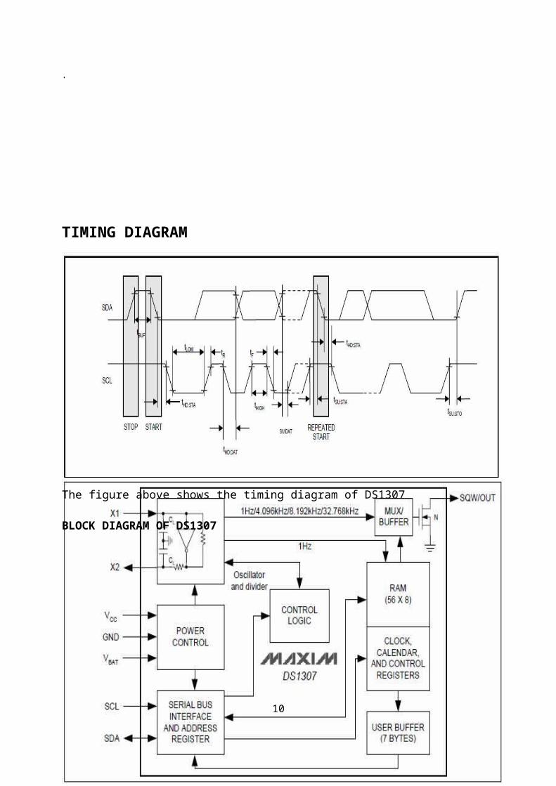
TIMING DIAGRAM
The figure above shows the timing diagram of DS1307
BLOCK DIAGRAM OF DS1307
7
The figure above represents the block diagram of DS1307
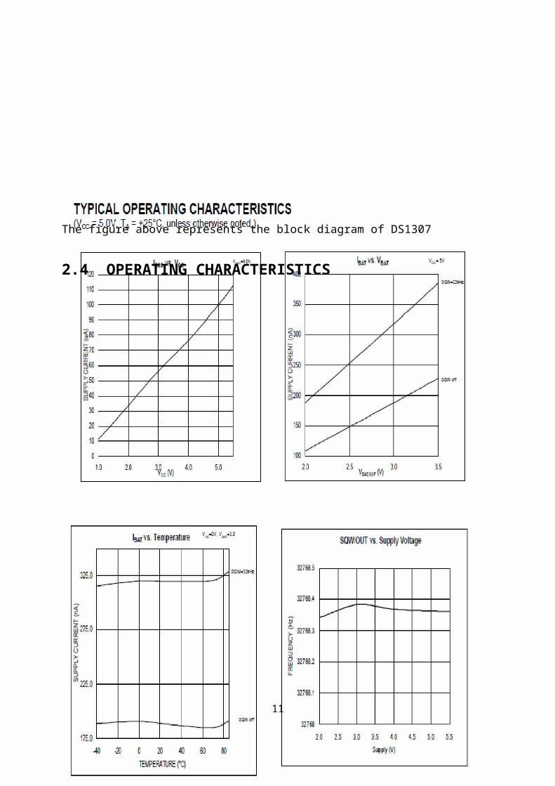
2.4 OPERATING CHARACTERISTICS
8
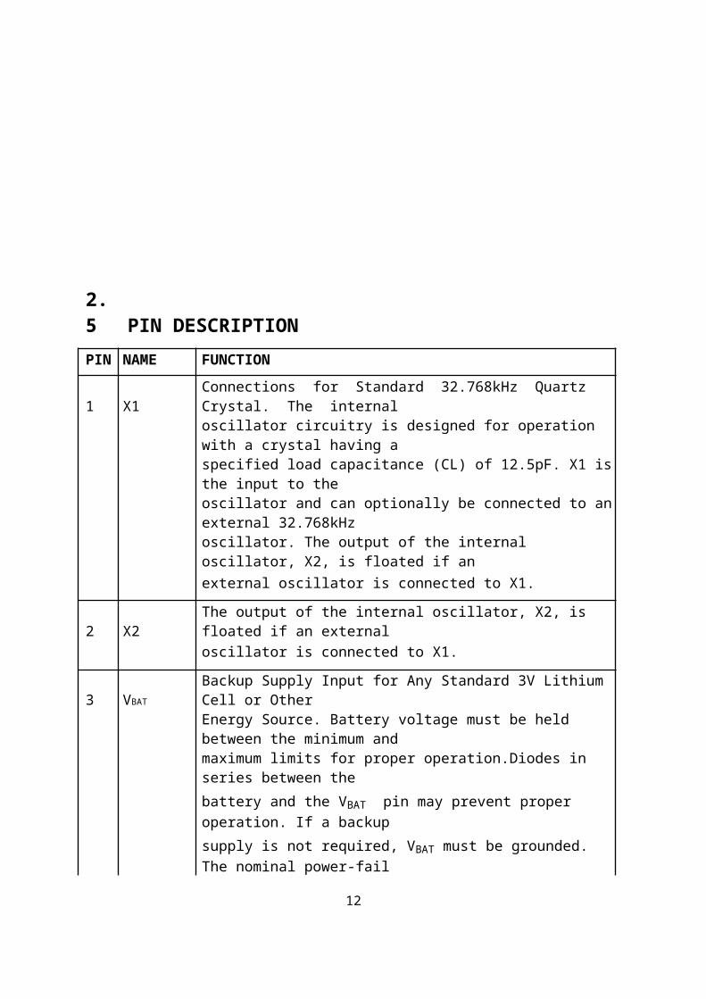
2.5 PIN DESCRIPTION
PIN NAME FUNCTION
1 X1 Connections for Standard 32.768kHz Quartz Crystal. The internal
oscillator circuitry is designed for operation with a crystal having a
specified load capacitance (CL) of 12.5pF. X1 is the input to the
oscillator and can optionally be connected to an external 32.768kHz
oscillator. The output of the internal oscillator, X2, is floated if an
external oscillator is connected to X1.
2 X2 The output of the internal oscillator, X2, is floated if an external
oscillator is connected to X1.
3 VBAT Backup Supply Input for Any Standard 3V Lithium Cell or Other
Energy Source. Battery voltage must be held between the minimum and
maximum limits for proper operation.Diodes in series between the
battery and the VBAT pin may prevent proper operation. If a backup
supply is not required, VBAT must be grounded. The nominal power-fail
trip point (VPF) voltage at which access to the RTC and user RAM is
denied is set by the internal circuitry as 1.25 x VBAT nominal. Alithium battery with 48mAh or greater will back up the DS1307 for more
than 10 years in the absence of power at +25°C.
4 GND Ground
5 SDA Serial Data Input/Output. SDA is the data input/output for the I2C serialinterface. The SDA pin is open drain and requires an external pullup
resistor. The pullup voltage can be up to 5.5V regardless of the voltage
on VCC.
6 SCL Serial Clock Input. SCL is the clock input for the I2C interface and isused to synchronize data movement on the serial interface. The pullup
voltage can be up to 5.5V regardless of the voltage on VCC
7 SQW/OUT Square Wave/Output Driver. When enabled, the SQWE bit set to 1, the
SQW/OUT pin outputs one of four square-wave frequencies (1Hz,
4kHz, 8kHz, 32kHz). The SQW/OUT pin is open drain and requires an
external pullup resistor. SQW/OUT operates with either VCC or VBAT
9
applied. The pullup voltage can be up to 5.5V regardless of the voltage
on VCC. If not used, this pin can be left floating.
8 VCC Primary Power Supply. When voltage is applied within normal limits,
the device is fully accessible and data can be written and read. When a
backup supply is connected to the device and VCC is below VTP, read and
writes are inhibited. However, the timekeeping function continues
unaffected by the lower input voltage.
2.6 DETAILED DESCRIPTION
The DS1307 is a low-power clock/calendar with 56 bytes of battery-backed SRAM. The
clock/calendar provides seconds,minutes, hours, day, date, month, and year information. The date
at the end of the month is automatically adjusted for months with fewer than 31 days, including
corrections for leap year. The DS1307 operates as a slave device on the I2C bus. Access is
obtained by implementing a START condition and providing a device identification code
followed by a register address. Subsequent registers can be accessed sequentially until a STOP
condition is executed. When VCC falls below 1.25 x VBAT, the device terminates an access in
progress and resets the device address counter. Inputs to the device will not be recognized at this
time to prevent erroneous data from being written to the device from an out-of-tolerance system.
When VCC falls below VBAT, the device switches into a lowcurrent battery-backup mode. Upon
power-up, the device switches from battery to VCC when VCC is greater than VBAT +0.2V and
recognizes inputs when VCC is greater than 1.25 x VBAT.
2.7 OSCILLATOR CIRCUIT
The DS1307 uses an external 32.768kHz crystal. The oscillator circuit does not
require any external resistors or capacitors to operate. Table 1 specifies several crystal
parameters for the external crystal. Figure shows a functional schematic of the oscillator
circuit. If using a crystal with the specified characteristics, the startup time is usually less than
one second.
10
CLOCK ACCURACY
The accuracy of the clock is dependent upon the accuracy of the crystal and the
accuracy of the match between the capacitive load of the oscillator circuit and the capacitive
load for which the crystal was trimmed. Additional error will be added by crystal frequency
drift caused by temperature shifts. External circuit noise coupled into the oscillator circuit
may result in the clock running fast.
2.9 CLOCK AND CALENDAR
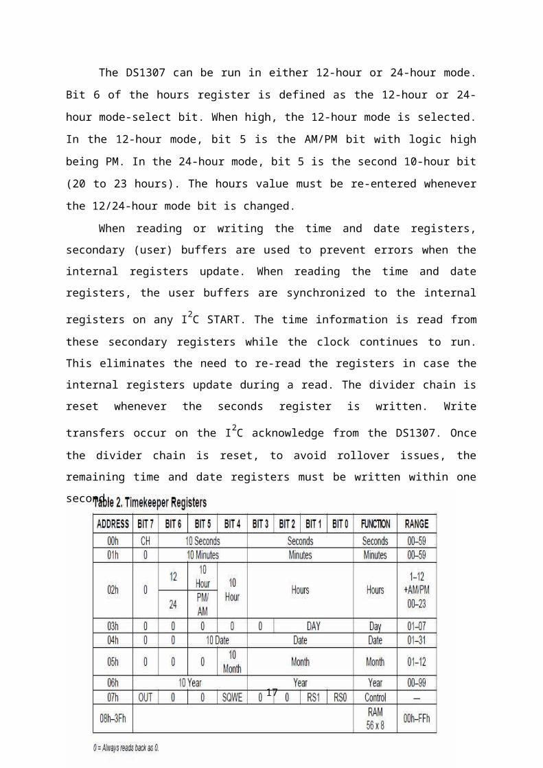
The time and calendar information is obtained by reading the appropriate register
bytes. Table 2 shows the RTC registers. The time and calendar are set or initialized by
writing the appropriate register bytes. The contents of the time and calendar registers are in
the BCD format. The day-of-week register increments at midnight. Values that correspond to
the day of week are user-defined but must be sequential (i.e., if 1 equals Sunday, then 2
equals Monday, and so on.) Illogical time and date entries result in undefined operation. Bit 7
of Register 0 is the clock halt (CH) bit. When this bit is set to 1, the oscillator is disabled.
When cleared to 0, the oscillator is enabled. On first application of power to the device the
time and date registers are typically reset to 01/01/00 01 00:00:00 (MM/DD/YY DOW
HH:MM:SS). The CH bit in the seconds register will be set to a 1. The clock can be halted
whenever the timekeeping functions are not required, which minimizes current (IBATDR).
The DS1307 can be run in either 12-hour or 24-hour mode. Bit 6 of the hours register
is defined as the 12-hour or 24-hour mode-select bit. When high, the 12-hour mode is
selected. In the 12-hour mode, bit 5 is the AM/PM bit with logic high being PM. In the 24-
hour mode, bit 5 is the second 10-hour bit (20 to 23 hours). The hours value must be re-
entered whenever the 12/24-hour mode bit is changed.
When reading or writing the time and date registers, secondary (user) buffers are used
to prevent errors when the internal registers update. When reading the time and date registers,
the user buffers are synchronized to the internal registers on any I2C START. The time
information is read from these secondary registers while the clock continues to run. This
eliminates the need to re-read the registers in case the internal registers update during a read.
The divider chain is reset whenever the seconds register is written. Write transfers occur on
the I2C acknowledge from the DS1307. Once the divider chain is reset, to avoid rollover
11
issues, the remaining time and date registers must be written within one second.
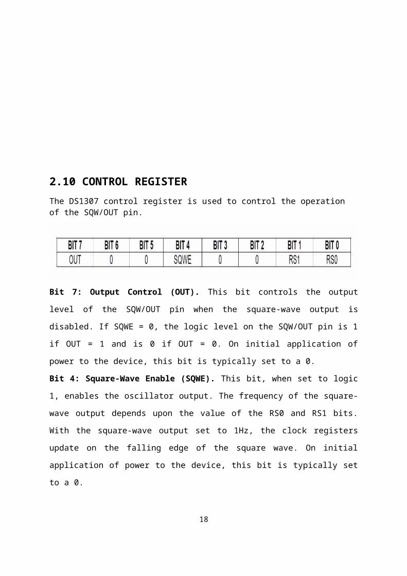
2.10 CONTROL REGISTER
The DS1307 control register is used to control the operation of the SQW/OUT pin.
Bit 7: Output Control (OUT). This bit controls the output level of the SQW/OUT pin when
the square-wave output is disabled. If SQWE = 0, the logic level on the SQW/OUT pin is 1 if
OUT = 1 and is 0 if OUT = 0. On initial application of power to the device, this bit is
typically set to a 0.
Bit 4: Square-Wave Enable (SQWE). This bit, when set to logic 1, enables the oscillator
output. The frequency of the square-wave output depends upon the value of the RS0 and RS1
bits. With the square-wave output set to 1Hz, the clock registers update on the falling edge of
12
the square wave. On initial application of power to the device, this bit is typically set to a 0.
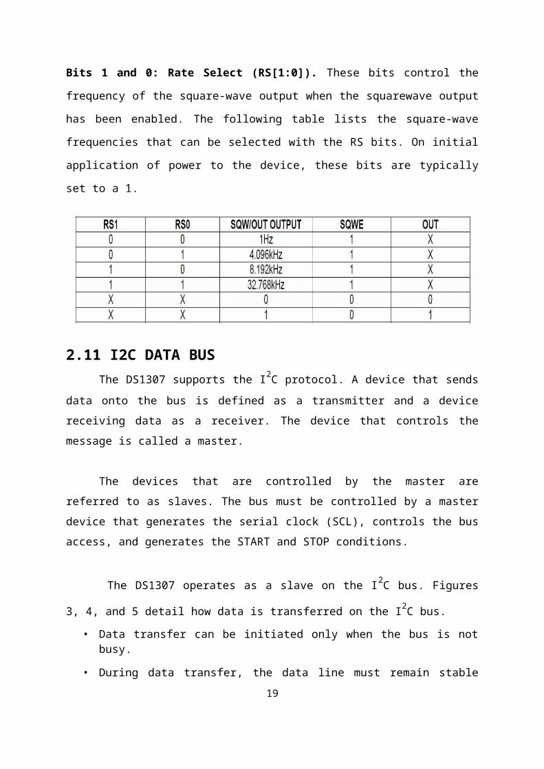
Bits 1 and 0: Rate Select (RS[1:0]). These bits control the frequency of the square-wave
output when the squarewave output has been enabled. The following table lists the square-
wave frequencies that can be selected with the RS bits. On initial application of power to the
device, these bits are typically set to a 1.
2.11 I2C DATA BUS
The DS1307 supports the I2C protocol. A device that sends data onto the bus is
defined as a transmitter and a device receiving data as a receiver. The device that controls the
message is called a master.
The devices that are controlled by the master are referred to as slaves. The bus must
be controlled by a master device that generates the serial clock (SCL), controls the bus
access, and generates the START and STOP conditions.
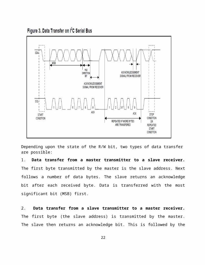
The DS1307 operates as a slave on the I2C bus. Figures 3, 4, and 5 detail how data is
transferred on the I2C bus.
• Data transfer can be initiated only when the bus is not busy.
• During data transfer, the data line must remain stable whenever the clock line is
HIGH. Changes in the data line while the clock line is high will be interpreted as
control signals.
13
Accordingly, the following bus conditions have been defined:
Bus not busy: Both data and clock lines remain HIGH.
START data transfer: A change in the state of the data line, from HIGH to LOW, while the clock is HIGH, defines a START condition.
STOP data transfer: A change in the state of the data line, from LOW to HIGH, while the
clock line is HIGH, defines the STOP condition.
Data valid: The state of the data line represents valid data when, after a START condition,
the data line is stable for the duration of the HIGH period of the clock signal. The data on the
line must be changed during the LOW period of the clock signal. There is one clock pulse per
bit of data. Each data transfer is initiated with a START condition and terminated with a
STOP condition. The number of data bytes transferred between START and STOP conditions
is not limited, and is determined by the master device. The information is transferred byte-
wise and each receiver acknowledges with a ninth bit. Within the I2C bus specifications a
standard mode (100kHz clock rate) and a fast mode (400kHz clock rate) are defined.
The DS1307 operates in the standard mode (100kHz) only.
Acknowledge: Each receiving device, when addressed, is obliged to generate an
acknowledge after the reception of each byte. The master device must generate an extra clock
pulse which is associated with this acknowledge bit. A device that acknowledges must pull
down the SDA line during the acknowledge clock pulse in such a way that the SDA line is
stable LOW during the HIGH period of the acknowledge related clock pulse. Of course, setup
and hold times must be taken into account. A master must signal an end of data to the slave
by not generating an acknowledge bit on the last byte that has been clocked out of the slave.
In this case, the slave must leave the data line HIGH to enable the master to generate the
STOP condition.
14
Depending upon the state of the R/W bit, two types of data transfer are possible:
1. Data transfer from a master transmitter to a slave receiver. The first byte transmitted by the
master is the slave address. Next follows a number of data bytes. The slave returns an acknowledge
bit after each received byte. Data is transferred with the most significant bit (MSB) first.
2. Data transfer from a slave transmitter to a master receiver. The first byte (the slave address) is
transmitted by the master. The slave then returns an acknowledge bit. This is followed by the slave
transmitting a number of data bytes. The master returns an acknowledge bit after all received bytes
other than the last byte. At the end of the last received byte, a “not acknowledge” is returned.
The master device generates all the serial clock pulses and the START and STOP conditions.
A transfer is ended with a STOP condition or with a repeated START condition. Since a repeated
START condition is also the beginning of the next serial transfer, the bus will not be released. Data is
transferred with the most significant bit (MSB) first.
15
A BRIEF INTRODUCTION TO 8051 MICROCONTROLLER:
When we have to learn about a new computer we have to familiarize about the machine
capability we are using, and we can do it by studying the internal hardware design (devices
architecture), and also to know about the size, number and the size of the registers.
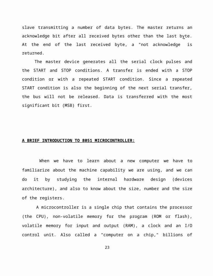
A microcontroller is a single chip that contains the processor (the CPU), non-volatile
memory for the program (ROM or flash), volatile memory for input and output (RAM), a clock and
an I/O control unit. Also called a "computer on a chip," billions of microcontroller units (MCUs) are
embedded each year in a myriad of products from toys to appliances to automobiles. For example, a
single vehicle can use 70 or more microcontrollers. The following picture describes a general block
diagram of microcontroller.
AT89S52: The AT89S52 is a low-power, high-performance CMOS 8-bit microcontroller with 8K
bytes of in-system programmable Flash memory. The device is manufactured using Atmel’s high-
density nonvolatile memory technology and is compatible with the industry-standard 80C51
instruction set and pin out. The on-chip Flash allows the program memory to be reprogrammed in-
system or by a conventional nonvolatile memory programmer.The AT89S52 provides the following
standard features: 8K bytes of Flash, 256 bytes of RAM, 32 I/O lines, Watchdog timer, two data
pointers, three 16-bit timer/counters, a six-vector two-level interrupt architecture, a full duplex serial
port, on-chip oscillator, and clock circuitry. In addition, the AT89S52 is designed with static logic for
operation down to zero frequency and supports two software selectable power saving modes. The
Idle Mode stops the CPU while allowing the RAM, timer/counters, serial port, and interrupt system
to continue functioning. The Power-down mode saves the RAM con-tents but freezes the oscillator,
disabling all other chip functions until the next interrupt.
16
The hardware is driven by a set of program instructions, or software. Once familiar with
hardware and software, the user can then apply the microcontroller to the problems easily.
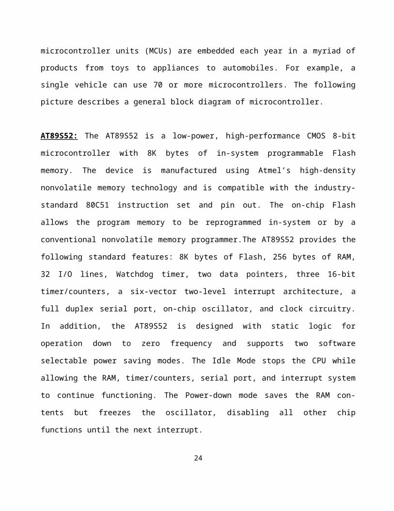
The pin diagram of the 8051 shows all of the input/output pins unique to microcontrollers:
17
The following are some of the capabilities of 8051 microcontroller.
1 Internal ROM and RAM
2 I/O ports with programmable pins
3 Timers and counters
4 Serial data communication
The 8051 architecture consists of these specific features:
16 bit PC &data pointer (DPTR) 8
bit program status word (PSW) 8
bit stack pointer (SP)
Internal ROM 4k
Internal RAM of 128 bytes.
4 register banks, each containing 8 registers 80
bits of general purpose data memory
32 input/output pins arranged as four 8 bit ports: P0-P3 Two 16 bit
timer/counters: T0-T1
Two external and three internal interrupt sources Oscillator and clock circuits.
18
HARDWARE DESCRIPTION:
1. POWER SUPPLY:
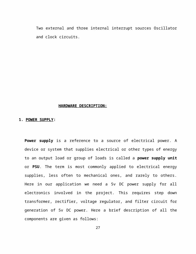
Power supply is a reference to a source of electrical power. A device or system that supplies
electrical or other types of energy to an output load or group of loads is called a power supply
unit or PSU. The term is most commonly applied to electrical energy supplies, less often to
mechanical ones, and rarely to others. Here in our application we need a 5v DC power supply for
all electronics involved in the project. This requires step down transformer, rectifier, voltage
regulator, and filter circuit for generation of 5v DC power. Here a brief description of all the
components are given as follows:
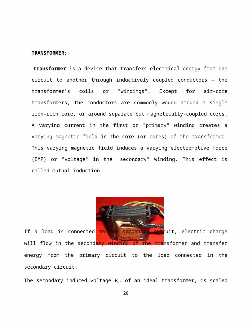
TRANSFORMER:
transformer is a device that transfers electrical energy from one circuit to another through
inductively coupled conductors — the transformer's coils or "windings". Except for air-core
transformers, the conductors are commonly wound around a single iron-rich core, or around
separate but magnetically-coupled cores. A varying current in the first or "primary" winding
creates a varying magnetic field in the core (or cores) of the transformer. This varying magnetic
field induces a varying electromotive force (EMF) or "voltage" in the "secondary" winding. This
effect is called mutual induction.
19
If a load is connected to the secondary circuit, electric charge will flow in the secondary winding of
the transformer and transfer energy from the primary circuit to the load connected in the secondary
circuit.
The secondary induced voltage VS, of an ideal transformer, is scaled from the primary VP by a factor
equal to the ratio of the number of turns of wire in their respective windings:
By appropriate selection of the numbers of turns, a transformer thus allows an alternating voltage to
be stepped up — by making NS more than NP — or stepped down, by making it
BASIC PARTS OF A TRANSFORMER
In its most basic form a transformer consists of:
A primary coil or winding.
A secondary coil or winding.
A core that supports the coils or windings.
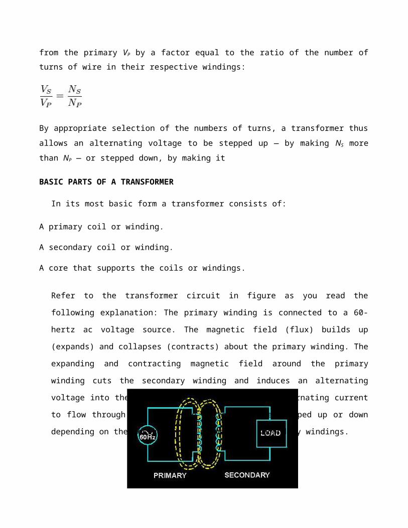
Refer to the transformer circuit in figure as you read the following explanation: The primary
winding is connected to a 60-hertz ac voltage source. The magnetic field (flux) builds up
(expands) and collapses (contracts) about the primary winding. The expanding and contracting
magnetic field around the primary winding cuts the secondary winding and induces an alternating
voltage into the winding. This voltage causes alternating current to flow through the load. The
voltage may be stepped up or down depending on the design of the primary and secondary
windings.
20
THE COMPONENTS OF A TRANSFORMER
Two coils of wire (called windings) are wound on some type of core material. In some cases the coils
of wire are wound on a cylindrical or rectangular cardboard form. In effect, the core material is air and
the transformer is called an AIR-CORE TRANSFORMER. Transformers used at low frequencies,
such as 60 hertz and 400 hertz, require a core of low-reluctance magnetic material, usually iron. This
type of transformer is called an IRON-CORE TRANSFORMER. Most power transformers are of the
iron-core type. The principle parts of a transformer and their functions are:
The CORE, which provides a path for the magnetic lines of flux. The PRIMARY WINDING,
which receives energy from the ac source. The SECONDARY WINDING, which receives
energy from the primary winding and delivers it to the load. The ENCLOSURE, which
protects the above components from dirt, moisture, and mechanical damage.
BRIDGE RECTIFIER
A bridge rectifier makes use of four diodes in a bridge arrangement to achieve full-wave rectification.
This is a widely used configuration, both with individual diodes wired as shown and with single
component bridges where the diode bridge is wired internally.
Basic operation
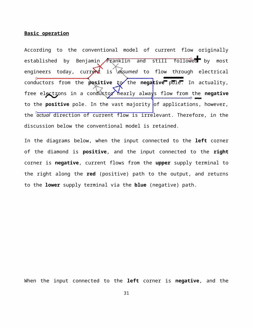
According to the conventional model of current flow originally established by Benjamin Franklin and
still followed by most engineers today, current is assumed to flow through electrical conductors from
the positive to the negative pole. In actuality, free electrons in a conductor nearly always flow from
the negative to the positive pole. In the vast majority of applications, however, the actual direction of
current flow is irrelevant. Therefore, in the discussion below the conventional model is retained.
In the diagrams below, when the input connected to the left corner of the diamond is positive, and the
input connected to the right corner is negative, current flows from the upper supply terminal to the
21
right along the red (positive) path to the output, and returns to the lower supply terminal via the blue
(negative) path.
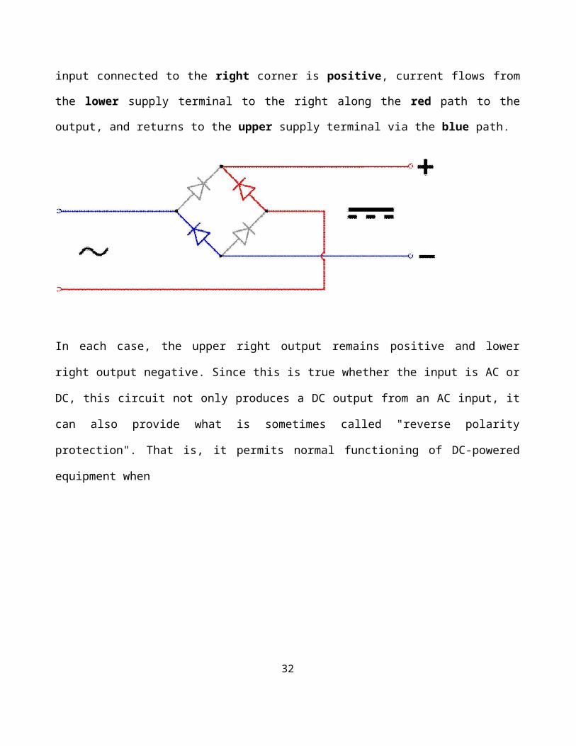
When the input connected to the left corner is negative, and the input connected to the right corner is
positive, current flows from the lower supply terminal to the right along the red path to the output,
and returns to the upper supply terminal via the blue path.
In each case, the upper right output remains positive and lower right output negative. Since this is true
whether the input is AC or DC, this circuit not only produces a DC output from an AC input, it can
also provide what is sometimes called "reverse polarity protection". That is, it permits normal
functioning of DC-powered equipment when
22
batteries have been installed backwards, or when the leads (wires) from a DC power source have been
reversed, and protects the equipment from potential damage caused by reverse polarity.
Prior to availability of integrated electronics, such a bridge rectifier was always constructed from
discrete components. Since about 1950, a single four-terminal component containing the four diodes
connected in the bridge configuration became a standard commercial component and is now available
with various voltage and current ratings.
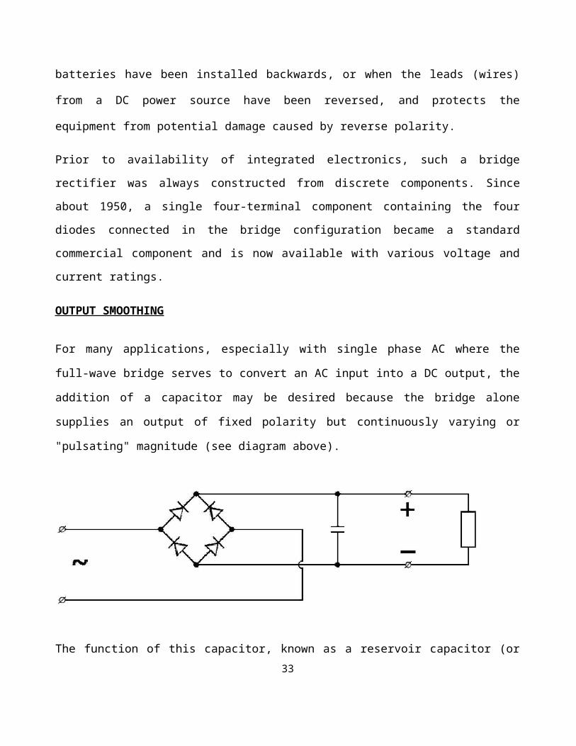
OUTPUT SMOOTHING
For many applications, especially with single phase AC where the full-wave bridge serves to convert
an AC input into a DC output, the addition of a capacitor may be desired because the bridge alone
supplies an output of fixed polarity but continuously varying or "pulsating" magnitude (see diagram
above).
The function of this capacitor, known as a reservoir capacitor (or smoothing capacitor) is to lessen the
variation in (or 'smooth') the rectified AC output voltage waveform from the bridge. One explanation
of 'smoothing' is that the capacitor provides a low impedance path to the AC component of the output,
reducing the AC voltage across, and AC current through, the resistive load. In less technical terms,
any drop in the output voltage and current of the bridge tends to be canceled by loss of charge in the
capacitor. This charge flows out as additional current through the load. Thus the change of load
current and voltage is reduced relative to what would occur without the capacitor. Increases of voltage
correspondingly store excess charge in the capacitor, thus moderating the change in output voltage /
current.
23
The simplified circuit shown has a well-deserved reputation for being dangerous, because, in some
applications, the capacitor can retain a lethal charge after the AC power source is removed. If
supplying a dangerous voltage, a practical circuit should include a reliable way to safely discharge the
capacitor. If the normal load cannot be guaranteed to perform this function, perhaps because it can be
disconnected, the circuit should include a bleeder resistor connected as close as practical across the
capacitor. This resistor should consume a current large enough to discharge the capacitor in a
reasonable time, but small enough to minimize unnecessary power waste.
Because a bleeder sets a minimum current drain, the regulation of the circuit, defined as percentage
voltage change from minimum to maximum load, is improved. However in many cases the
improvement is of insignificant magnitude.
The capacitor and the load resistance have a typical time constant τ = RC where C and R are the
capacitance and load resistance respectively. As long as the load resistor is large enough so that this
time constant is much longer than the time of one ripple cycle, the above configuration will produce a
smoothed DC voltage across the load.
In some designs, a series resistor at the load side of the capacitor is added. The smoothing can then be
improved by adding additional stages of capacitor–resistor pairs, often done only for sub-supplies to
critical high-gain circuits that tend to be sensitive to supply voltage noise.
The idealized waveforms shown above are seen for both voltage and current when the load on the
bridge is resistive. When the load includes a smoothing capacitor, both the voltage and the current
waveforms will be greatly changed. While the voltage is smoothed, as described above, current will
flow through the bridge only during the time when the input voltage is greater than the capacitor
voltage. For example, if the load draws an average current of n Amps, and the diodes conduct for 10%
of the time, the average diode current during conduction must be 10n Amps. This non-sinusoidal
current leads to harmonic distortion and a poor power factor in the AC supply.
In a practical circuit, when a capacitor is directly connected to the output of a bridge, the bridge diodes
must be sized to withstand the current surge that occurs when the power is turned on at the peak of the
24
AC voltage and the capacitor is fully discharged. Sometimes a small series resistor is included before
the capacitor to limit this current, though in most applications the power supply transformer's
resistance is already sufficient.
Output can also be smoothed using a choke and second capacitor. The choke tends to keep the current
(rather than the voltage) more constant. Due to the relatively high cost of an effective choke compared
to a resistor and capacitor this is not employed in modern equipment.
Some early console radios created the speaker's constant field with the current from the high voltage
("B +") power supply, which was then routed to the consuming circuits, (permanent magnets were
then too weak for good performance) to create the speaker's constant magnetic field. The speaker field
coil thus performed 2 jobs in one: it acted as a choke, filtering the power supply, and it produced the
magnetic field to operate the speaker.
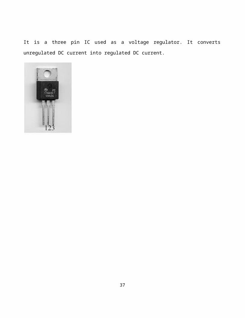
REGULATOR IC (78XX)
It is a three pin IC used as a voltage regulator. It converts unregulated DC current into regulated DC
current.
25
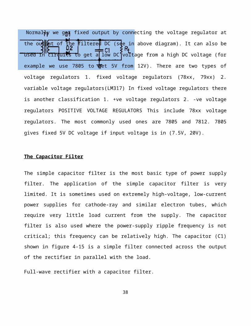
Normally we get fixed output by connecting the voltage regulator at the output of the filtered DC (see
in above diagram). It can also be used in circuits to get a low DC voltage from a high DC voltage (for
example we use 7805 to get 5V from 12V). There are two types of voltage regulators 1. fixed voltage
regulators (78xx, 79xx) 2. variable voltage regulators(LM317) In fixed voltage regulators there is
another classification 1. +ve voltage regulators 2. -ve voltage regulators POSITIVE VOLTAGE
REGULATORS This include 78xx voltage regulators. The most commonly used ones are 7805 and
7812. 7805 gives fixed 5V DC voltage if input voltage is in (7.5V, 20V).
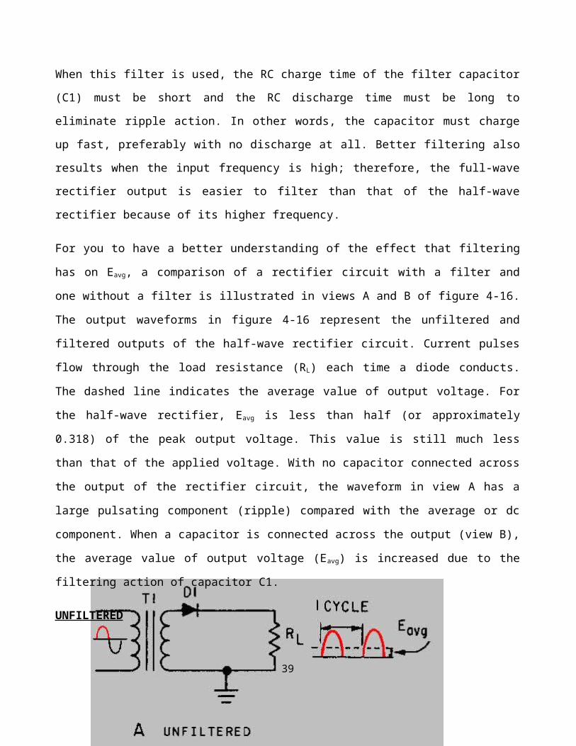
The Capacitor Filter
The simple capacitor filter is the most basic type of power supply filter. The application of the simple
capacitor filter is very limited. It is sometimes used on extremely high-voltage, low-current power
supplies for cathode-ray and similar electron tubes, which require very little load current from the
supply. The capacitor filter is also used where the power-supply ripple frequency is not critical; this
frequency can be relatively high. The capacitor (C1) shown in figure 4-15 is a simple filter connected
across the output of the rectifier in parallel with the load.
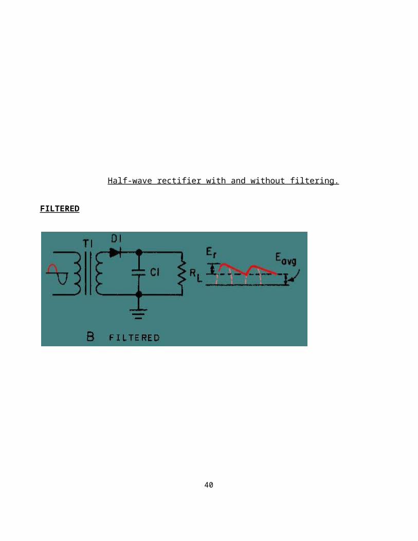
Full-wave rectifier with a capacitor filter.
When this filter is used, the RC charge time of the filter capacitor (C1) must be short and the RC
discharge time must be long to eliminate ripple action. In other words, the capacitor must charge up
fast, preferably with no discharge at all. Better filtering also results when the input frequency is high;
therefore, the full-wave rectifier output is easier to filter than that of the half-wave rectifier because of
its higher frequency.
For you to have a better understanding of the effect that filtering has on E avg, a comparison of a
rectifier circuit with a filter and one without a filter is illustrated in views A and B of figure 4-16. The
output waveforms in figure 4-16 represent the unfiltered and filtered outputs of the half-wave rectifier
circuit. Current pulses flow through the load resistance (RL) each time a diode conducts. The dashed
line indicates the average value of output voltage. For the half-wave rectifier, Eavg is less than half (or
26
approximately 0.318) of the peak output voltage. This value is still much less than that of the applied
voltage. With no capacitor connected across the output of the rectifier circuit, the waveform in view A
has a large pulsating component (ripple) compared with the average or dc component. When a
capacitor is connected across the output (view B), the average value of output voltage (Eavg) is
increased due to the filtering action of capacitor C1.
UNFILTERED
Half-wave rectifier with and without filtering.
FILTERED
27
The value of the capacitor is fairly large (several microfarads), thus it presents a relatively
low reactance to the pulsating current and it stores a substantial charge.
The rate of charge for the capacitor is limited only by the resistance of the conducting diode,
which is relatively low. Therefore, the RC charge time of the circuit is relatively short. As a
result, when the pulsating voltage is first applied to the circuit, the capacitor charges rapidly
and almost reaches the peak value of the rectified voltage within the first few cycles. The
capacitor attempts to charge to the peak value of the rectified voltage anytime a diode is
conducting, and tends to retain its charge when the rectifier output falls to zero. (The
capacitor cannot discharge immediately.) The capacitor slowly discharges through the load
resistance (RL) during the time the rectifier is non-conducting.
The rate of discharge of the capacitor is determined by the value of capacitance and the value
of the load resistance. If the capacitance and load-resistance values are large, the RC
discharge time for the circuit is relatively long.
3. OPERATION
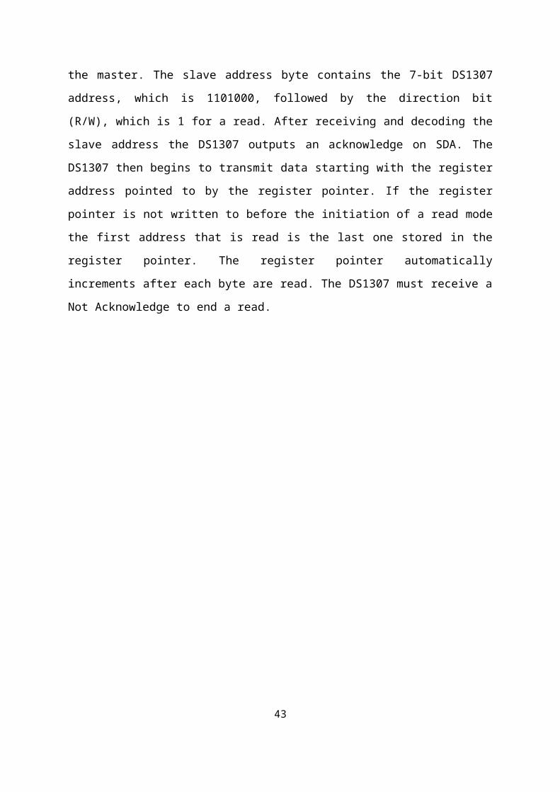
The DS1307 can operate in the following two modes:
1. Slave Receiver Mode (Write Mode): Serial data and clock are received through SDA and
SCL. After each byte is received an acknowledge bit is transmitted. START and STOP
conditions are recognized as the beginning and end of a serial transfer. Hardware performs
address recognition after reception of the slave address and direction bit (see Figure 4). The
slave address byte is the first byte received after the master generates the START condition.
The slave address byte contains the 7-bit DS1307 address, which is 1101000, followed by the
direction bit (R/W), which for a write is 0. After receiving and decoding the slave address
byte, the DS1307 outputs an acknowledge on SDA. After the DS1307 acknowledges the
slave address + write bit, the master transmits a word address to the DS1307. This sets the
register pointer on the DS1307, with the DS1307 acknowledging the transfer. The master can
then transmit zero or more bytes of data with the DS1307 acknowledging each byte received.
The register pointer automatically increments after each data byte are written. The master will
generate a STOP condition to terminate the data write.
28
2. Slave Transmitter Mode (Read Mode): The first byte is received and handled as in the
slave receiver mode. However, in this mode, the direction bit will indicate that the transfer
direction is reversed. The DS1307 transmits serial data on SDA while the serial clock is input
on SCL. START and STOP conditions are recognized as the beginning and end of a serial
transfer (see Figure 5). The slave address byte is the first byte received after the START
condition is generated by the master. The slave address byte contains the 7-bit DS1307
address, which is 1101000, followed by the direction bit (R/W), which is 1 for a read. After
receiving and decoding the slave address the DS1307 outputs an acknowledge on SDA. The
DS1307 then begins to transmit data starting with the register address pointed to by the
register pointer. If the register pointer is not written to before the initiation of a read mode the
first address that is read is the last one stored in the register pointer. The register pointer
automatically increments after each byte are read. The DS1307 must receive a Not
Acknowledge to end a read.
29
30
4. REAL-TIME CLOCK INTERFACING (DS1307)
WITH AT89C51
4.1 DESCRIPTION
This application note describes the general hardware configuration and basic software
communication examples for the Dallas I2C serial-interface Real-Time Clocks (RTC).The
devices covered are the BCD-format I2C clocks: DS1307, DS1337, DS1338, DS1339 and
DS1340.The DS1375 could also be supported, if circuit modifications were made to provide
digital clock signal (32,768Hz, 8,192Hz, 60H, or 50Hz) to the CLK input pin.The
microcontroller used for this example is the DS2250, and example software is written in C.
A schematic of the circuit is shown in Figure 1. The schematic shows connections for
a DS1340. The other RTCs may require modifications. The DS1337, for example, replaces
the battery back up input with an additional interrupt output. The low voltage versions of the
RTCs would require replacing the DS2250/DS5000 with a suitable low-voltage
microcontroller. Figure 2 shows the software listing. The #define directive is used to
conditionally compile the code for the proper device. The example shown is for the DS1307.
The #define statement for the DS1307 should be replaced with the correct device before
compiling the code
31
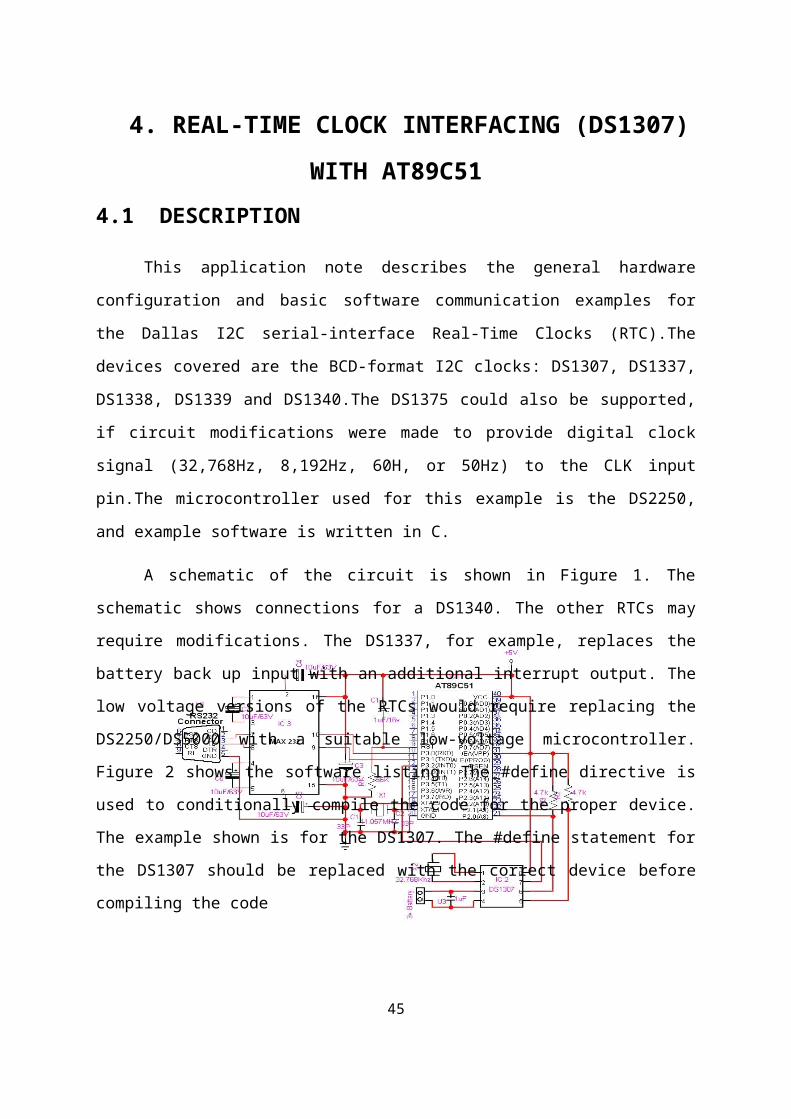
*********************************************************
******/ /* DEMO1307.c */
/*********************************************************
***********/
#include <at89x52.h> /* Prototypes for I/O functions */
#include <stdio.h>
/***************************** Defines *****************************/
#define ACK 0
#define NACK 1
#define ADDRTC 0xd0/* I2C slave address */
#define DS1307 /* compile directive, modify as required */
/************************* bit definitions *************************/
sbit scl = P2^0; /* I2C pin definitions */
sbit sda = P2^1;
sbit sqw = P3^2; /* pin function depends upon device */
void I2C_start();
void I2C_stop();
void I2C_write(unsigned char d);
uchar I2C_read(uchar);
void readbyte();
void writebyte();
void initialize();
24void disp_clk_regs(uchar);
void burstramwrite(uchar);
void burstramread();
void alrm_int();
void alrm_read();
void tc_setup();
/* global variables */
uchar sec, min, hr, dy, dt, mn, yr;
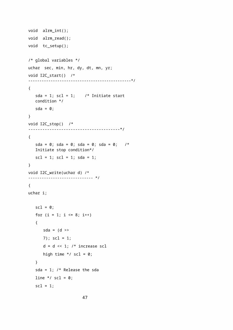
void I2C_start() /* ----------------------------------------------*/
{
sda = 1; scl = 1; /* Initiate start condition */
sda = 0;
32
}
void I2C_stop() /* ---------------------------------------*/
{
sda = 0; sda = 0; sda = 0; sda = 0; /* Initiate stop condition*/
scl = 1; scl = 1; sda = 1;
}
void I2C_write(uchar d) /* ----------------------------- */
{
uchar i;
scl = 0;
for (i = 1; i <= 8; i++)
{
sda = (d >> 7); scl
= 1;
d = d << 1; /* increase scl high time */ scl = 0;
}
sda = 1; /* Release the sda line */ scl = 0;
scl = 1;
if(sda) printf("Ack bit missing %02X",(unsigned int)d); scl
= 0;
}
uchar I2C_read(uchar b) /* ----------------------------------- */
{
uchar d, i;
sda = 1; /* Let go of sda line */
scl = 0;
for (i = 1; i <= 8; i++) /* read the msb first */
{
scl = 1;
d = d << 1;
d = d | (unsigned char)sda;
scl = 0;
}
sda = b; /* Hold sda low for acknowledge */
scl = 0;
33
scl = 1;
if(b == NACK) sda = 1; /* sda = 1 if next cycle is reset */ scl =
0;
sda = 1; /* Release the sda line */
return d;
}
void readbyte() /* -- read one byte of data from the specific address -- */
{
uchar Add;
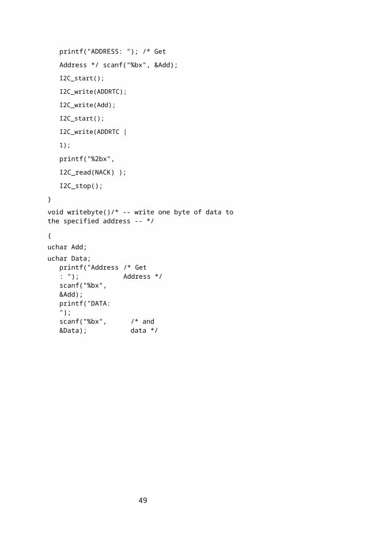
printf("ADDRESS: "); /* Get Address */
scanf("%bx", &Add);
I2C_start();
I2C_write(ADDRTC);
I2C_write(Add);
I2C_start();
I2C_write(ADDRTC | 1);
printf("%2bx",
I2C_read(NACK) ); I2C_stop();
}
void writebyte()/* -- write one byte of data to the specified address -- */
{
uchar Add;
uchar Data;
printf("Address: "); /* Get Address */
scanf("%bx", &Add);
printf("DATA: ");
scanf("%bx", &Data); /* and data */
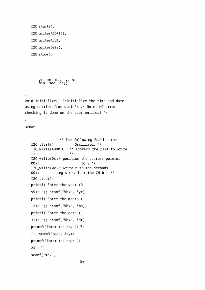
34
I2C_start();
I2C_write(ADDRTC);
I2C_write(Add);
I2C_write(Data); I2C_stop();
}
void initialize() /*initialize the time and date using entries from stdin*/ /*
Note: NO error checking is done on the user entries! */
{
uchar
I2C_start(); /* The following Enables the Oscillator */
I2C_write(ADDRTC); /* address the part to write */
I2C_write(0x00); /* position the address pointer to 0 */
I2C_write(0x00); /* write 0 to the seconds register,clear the CH bit */
I2C_stop();
printf("Enter the year (0-99): ");
scanf("%bx", &yr);
printf("Enter the month (1-12): ");
scanf("%bx", &mn); printf("Enter the date
(1-31): "); scanf("%bx", &dt);
printf("Enter the day (1-7): ");
scanf("%bx", &dy); printf("Enter the hour
(1-23): ");
scanf("%bx", &hr);
hr = hr & 0x3f; /* force clock to 24 hour mode */
printf("Enter the minute (0-59): ");
scanf("%bx", &min);
printf("Enter the second (0-59): ");
scanf("%bx", &sec);
I2C_start();
I2C_write(ADDRTC); /* write slave address + write */
35
yr, mn, dt, dy, hr, min, sec, day;
I2C_write(0x00); /* write register address, 1st clock register */
I2C_write(sec);
I2C_write(min);
I2C_write(hr);
I2C_write(dy);
I2C_write(dt); I2C_write(mn);
I2C_write(yr);
#if defined DS1307 || defined DS1338
{
I2C_write(0x10); /* enable sqwe, 1Hz output */
}
#elif defined DS1337 || defined DS1339
{
I2C_start();
I2C_write(ADDRTC); /* write slave address + write */
I2C_write(0x0e); /* write register address, control register */
I2C_write(0x20); /* enable osc, bbsqi */
I2C_write(0); /* clear OSF, alarm flags */
/* could enable trickle charger here */
}
#elif defined DS1340
I2C_write(0x10); /* enable sqwe, 1Hz output */
I2C_start(); /* address pointer wraps at 7, so point to flag register */
I2C_write(ADDRTC); /* write slave address + write */
I2C_write(0x09); /* write register address, control register */
I2C_write(0); /* clear OSF */
}
#endif
I2C_stop();
}
void disp_clk_regs(uchar prv_sec) /* ----------------------------------------- */
{
uchar Sec, Min, Hrs, Dte, Mon, Day, Yr, mil, pm;
printf("Yr Mn Dt Dy Hr:Mn:Sc");
while(!RI) /* Read & Display Clock Registers */
36
{
I2C_start();
I2C_write(ADDRTC); /* write slave address + write */
I2C_write(0x00); /* write register address, 1st clock register */
I2C_start();
I2C_write(ADDRTC | 1); /* write slave address + read */
37
Sec = I2C_read(ACK); /* starts w/last address stored in register pointer */
Min = I2C_read(ACK);
Hrs = I2C_read(ACK);
Day = I2C_read(ACK);
Dte = I2C_read(ACK);
Mon = I2C_read(ACK);
Yr = I2C_read(NACK);
I2C_stop();
if(Hrs & 0x40)
mil = 0;
else
mil = 1;
if(Sec != prv_sec) /* display every time seconds change */
{
if(mil)
{
printf("%02bX/%02bX/%02bX
%2bX", Yr, Mon, Dte, Day);
printf(" %02bX:%02bX:
%02bX", Hrs, Min, Sec);
}
else
{
if(Hr
s
&
0
x
2
0
)
p
m
=
38
'
A
'
;
else
pm = 'P';
Hrs &= 0x1f; /* strip mode and am/pm
bits */ printf("%02bx/%02bx/%02bx
%02bx", Yr, (Mon & 0x1f), Dte, Day);
printf(" %02bx:%02bx:%02bx %cM",
Hrs, Min, Sec, pm);
}
}
if
(
p
r
v
_
s
e
c
=
=
0
x
f
e
)
r
e
t
u
r
n
;
p
r
39
v
_
s
e
c
=
S
e
c
;
}
RI = 0; /* Swallow keypress before exiting */
}
void burstramwrite(uchar Data) /* -------- fill RAM with data -------- */
{
uchar j;
I2C_start();I2C_write(ADDRTC); /* write slave address + write */
I2C_write(0x08); /* write register address, 1st RAM location */
for (j = 0; j < 56; j++) /* write until the pointer wraps around */
{
I2C_write(Data);
}
I2C_stop();
}
void burstramread() /* ----------------------------------------- */
{
uchar j;
I2C_start();
I2C_write(ADDRTC); /* write slave address + write */
I2C_write(8); /* write register address, 1st RAM location -1*/
I2C_start();
I2C_write(ADDRTC | 1); /* write slave address + read */
for (j = 0; j < 56; j++)
40
{
if(!(j % 16)) printf("%02bX ", j);
printf("%02bX ", I2C_read(ACK) );
}
I2C_read(NACK);
I2C_stop();
}
void alrm_int() /* ----- initialize alarm registers ------ */
{
uchar M, Sec, Min, Hr, DyDt;
printf("1-Alarm each second 2-Alarm match=sec 3-Alarm match=sec+min");
printf("4-Alarm match=sec+min+hr 5-Alarm match=sec+min+hr+date");
printf("6-Alarm match=sec+min+hr+day Enter selection: ");
M = _getkey(); /* Note-No error checking is done on entries! */
switch(M)
{
case '1': M = 0xf; break;
case '2':M =
0xe;
break;ase '3': M = 0xc; break;
case '4': M = 8; break;
case '5': M = 0; break;
case '6': M = 0x40; break;
}
if(M & 0x40)
{
printf("Enter the day (1-7):
"); scanf("%bx", &DyDt);
}
else
{
41
printf("Enter the date (1-31): ");
scanf("%bx", &DyDt);
}
printf("Enter the hour (1-23):
"); scanf("%bx", &Hr);
printf("Enter the minute (0-59): ");
scanf("%bx", &Min);
printf("Enter the second (0-59): ");
scanf("%bx", &Sec);
if( (M & 1) ) Sec |= 0x80;
if( ((M >> 1) & 1) ) Min |= 0x80;
if( ((M >> 2) & 1) ) Hr |= 0x80;
if( ((M >> 3) & 1) ) DyDt |= 0x80;
if(M & 0x40) DyDt |= 0x40;
I2C_start();
I2C_write(ADDRTC); /* write slave address + write */
I2C_write(7); /* write register address */
I2C_write(Sec);
I2C_write(Min);
I2C_write(Hr);
I2C_write(DyDt);
I2C_start();
I2C_write(ADDRTC); /* write slave address + write */
I2C_write(0x0e); /* write register address */
I2C_write(5); /* enable interrupts, alarm 1 */
I2C_stop();
1
42
}
void alrm_read() /* ----- read alarm registers ------ */
{
uchar Sec, Min, Hr, DyDt;
I2C_start();
I2C_write(ADDRTC); /* write slave address + write */
I2C_write(7); /* write register address */
I2C_start();
I2C_write(ADDRTC | 1); /* write slave address + read */
Sec = I2C_read(ACK);
Min = I2C_read(ACK);
Hr = I2C_read(ACK);
DyDt = I2C_read(NACK);
printf("Alarm 1: %02bx %02bx %02bx %02bx", Sec, Min, Hr, DyDt);
}
void tc_setup() /* ---- trickle charger set up routine ---- */
{
uchar M, val;
#if defined DS1339
#define TC 0x10 /* address for DS1339 trickle charge register */
#else
#define TC 0x08 /* address for DS1340 trickle charge register */
#endif
printf("Enable Trickle Charger (Y/N)? "); M = _getkey();
if(M == 'Y' || M == 'y')
{
printf("1-250 ohm res2-2K res=sec3-4K res");
M = _getkey(); /* Note-No error checking is done on entries! */
switch(M)
{
case '1': val = 1; break;
case '2': val = 2; break;case '3': val = 3; break;
43
}
printf("1-no diode2-1 diode");
M = _getkey(); /* Note-No error checking is done on entries! */
switch(M)
{
case '1': val += 4; break;
case '2': val += 8; break;
}
I2C_start();
I2C_write(ADDRTC); /* write slave address + write */
I2C_write(TC); /* write register address */
I2C_write(val | 0xa0); /* enable trickle charger per user input */
I2C_stop();
}
else
{
I2C_start();
I2C_write(ADDRTC); /* write slave address + write */
I2C_write(TC); /* write register address */
I2C_write(0); /* disable trickle charger */
I2C_stop();
}
I2C_start();
I2C_write(ADDRTC); /* write slave address + write */
I2C_write(TC); /* write register address */
I2C_start();
I2C_write(ADDRTC | 1); /* write slave address + read */
printf("Trickle Charger: %02bx", I2C_read(NACK) );
}
main (void) /* ----------------------------------------------------- */
{
uchar M, M1;
sqw = 1; /* set up for read, weak pull-up */
while (1)
{ #if defined DS1307
44
printf("DEMO1307 build %s", __DATE__); #elif defined DS1337
printf("DEMO1337 build %s", __DATE__); #elif defined DS1338
printf("DEMO1338 build %s", __DATE__); #elif defined DS1339
printf("DEMO1339 build %s", __DATE__); #elif defined DS1340
printf("DEMO1340 build %s", __DATE__);
#endif
printf("CI Init RTC CR Read Clock");
printf("BR Byte Read BW Write Byte");
#if defined DS1337 || defined DS1339 /* only print if part has alarms */
printf("AI Alarm 1 Int AR Alarm Read");
#endif
#if defined DS1340 || defined DS1339 /* parts that have trickle charger */ printf("Tc Trickle charger");
#endif
#if defined DS1307 || defined DS1338 /* only print if part has RAM */ printf("RR RAM Read RW RAM
Write");
#endif
printf("Enter Menu Selection:");
4.2 RTC PROGRAM
#include<reg51.h>
#include<stdio.h>
#include<ds1307.h> void delay(int);
unsigned char RTC_ARR[7]; // Buffer for second,minute,.....,year
unsigned char p; void main(void)
{
TMOD=0x20;
SCON=0x52;
TH1=0xFD;
TR1=1;
45
// Setup time and enable oscillator
//-----------------------------------
ReadRTC(&RTC_ARR[0]);
RTC_ARR[0] = RTC_ARR[0] & 0x7F; // enable oscillator (bit 7=0)
RTC_ARR[1] = 0x50; // minute = 59
RTC_ARR[2] = 0x12; // hour = 05 ,24-hour mode(bit 6=0)
RTC_ARR[3] = 0x03; // Day = 1 or sunday
RTC_ARR[4] = 0x10; // Date = 30
RTC_ARR[5] = 0x08; // month = August
RTC_ARR[6] = 0x10; // year = 05 or 2005
WriteRTC(&RTC_ARR[0]); // Set RTC
//-----------------------------------
while(1)
{ if(RTC_ARR[1]==0x51)
P1=0xaa;
if(RTC_ARR[1]==0x52)
P1=0x55;
ReadRTC(&RTC_ARR[0]);
putchar(0x0C); // clear Hyper terminal
printf("calender \n");
printf("Day : %s\r\n",Int2Day(RTC_ARR[3]));
printf("Time : %02bX:%02bX:%02bX\r\n",RTC_ARR[2],RTC_ARR[1],RTC_ARR[0]);
printf("Date : %02bX-%s-
20%02bX",RTC_ARR[4],Int2Month(RTC_ARR[5]),RTC_ARR[6]);
46
//
delay(10000); // delay about 1 second
}
}
void delay(int time)
{
int i,j; for(i=0;i<time;i++); for(j=0;j<5000;j++);
}
47
4.3 CIRCUIT
48
5. APPLICATIONS OF RTC
• A real time clock (RTC) circuit may be used to maintain rough GPS time while the
rest of the GPS circuitry is off. The global positioning system (GPS) is a collection of
twenty-four earth-orbiting satellites. Each of the GPS satellites travels in a precise orbit
about 11,000 miles above the earth's surface. A GPS receiver locks onto at least three of
the satellites to determine its precise location.
• Data recorders for collecting and managing vehicle operational data or messages are
known in the automotive and heavy duty truck industries. Data analyzers having such
capability are thus able to link the vehicle operational data to vehicle operating
conditions existing during data recordation such as a particular driver or group of
drivers, weather conditions, geographic locations, road grade conditions encountered,
and other vehicle operating conditions. Real time clocks are incorporated in electronic
data recorders to "time-stamp" the vehicle operational data or messages as they are
recorded.
• Real time clock is also used in managed network elements for time stamping event
reports sourced from the respective element. Such reports may, for example, be the start
or finish times of a traffic connection
Clock circuits are an essential component of modern computer systems
• A typical computer system includes a processor subsystem of one or more microprocessor, a memory
49
subsystem, one or more chipsets provided to support different types of host processors for
different platforms such as desktops, personal computers (PC), servers, workstations and mobile
platforms, and to provide an interface with a plurality of input/output (I/O) devices. Chipsets may
integrate a largeamount of I/O bus interface circuitry and other circuitry onto only a few chips.
These chipsets may implement the I/O bus interface circuitry, timer, real-time clock (RTC), direct
memory access (DMA) controller, and other additional functionality such as integrated power and
thermal management with quick resume capabilities and random seed number generation for
security applications such as cryptography, digital signatures, and protected communication
protocols. Clock circuits generate a regular series of pulses based on a piezoelectric crystal, which
governs the frequency of the pulses. The clock signal that is generated is used to synchronize the
operation of the other components and circuits in the system. The boot up operation of a computer
system is reliant upon the establishment of a reliable system clock. Establishing this reliable signal
adds additional time to the boot up process for a system.
• A typical personal computer includes two time keeping systems: a hardware real time clock,
and a software virtual clock maintained by an operating system. The hardware real time
clock typically includes a battery backup source of electrical power, and continuously
maintains an estimate of the current date and time. The software virtual clock is typically
synchronized to the RTC during PC power up and initialization.
On a computer mother board, a RTC is provided to maintain the data stored in a
CMOS on the mother board. Generally, electrical power is provided to a RTC by a battery
arranged on the mother board. The RTC is used to update the current time and date within
the computer system without any intervention from the system processor. Usually the RTC
and other peripheral devices are coupled to the peripheral bus through an interrupt
controller. Such a clock has various uses such as time stamping files and inserting dates into
documents.
• The RTC is used to update a program clock, typically a date/time clock maintained by the
operating system (OS) and referred to herein as the OS clock. An operating system may
include a system clock to provide a system time for measuring small increments of time.
The system clock may update the system clock in response to a periodic interrupt generated
50
by a system timer, or a real time clock event timer.
• A personal digital assistant (PDA) is a pen-based computer system where the
primary method for inputting data includes a pen or stylus. Many of the functions of a
PDA require an accurate real-time clock to provide the calendar function, the clock
display, and various timer functions of a PDA require an accurate real-time clock.
• An electronic apparatus generally has a RTC (real time clock) installed in the circuit
board thereof for recording system time. A real time clock is one of the requisite
hardware devices of an electronic device. A standard RTC includes an oscillating circuit
coupled to a digital counter.
• A typical real time clock can be programmed to produce or generate an RTC alarm
event at a designated time. The RTC alarm event may cause, for example, the assertion
of an interrupt signal to the microprocessor
• A real time clock is typically implemented in specific hardware with a dedicated
crystal oscillator to insure accuracy and a battery backup power supply to insure
preservation of timekeeping data during an interruption of the primary power supply.
This is especially important with personal computers which are frequently powered
down. It is common to back up a real-time clock (RTC) with a battery, such as a long-
life lithium battery, so that when a main power supply for the RTC fails, or has been
disconnected, the RTC will continue to indicate the correct time and provide correct time
intervals.
51
52
53
6. CONCLUSION
Real time clocks can be much more accurate than other time-keeping alternatives,
they allow the main system to perform important tasks, and they do not consume much
power. Electronic devices can even increase their functionality by using real-time clocks.
Certain electronic devices can rely on real-time clocks when comparing the times of previous
functions. If the functions have taken place within a designated period of time, device
functions can be reduced drastically.
Hence real time clocks using microcontrollers are used extensively in controlling
home appliances
44
54