Embed Size (px)
Citation preview

STMicroelectronics
®
RTP n° 21Paris, le 5 Novembre 2003
Evolution de la conception des « systèmes surune puce » à l’ère des nanotechnologies
Jean-Pierre SCHOELLKOPF
Central R&D, Crolles, France

®11-03 2
Agenda
Technology Evolution
New system requirements
Hardware/Software co-design
Design Complexity and manufacturing costs
Concurrent hard/software design and validation
Flexible and Reconfigurable SoC
Conclusion

®11-03 3
90nm full SiOC/Cu interconnect

®11-03 4
65nm Process Development – Crolles2
0.69um2 Bitcell
Active
Poly
Bitcell Design
45nm Gate – (180nm Pitch)
45nm
135nm
Line1 patterning – (200nm Pitch)Contact polish – (200nm Pitch)
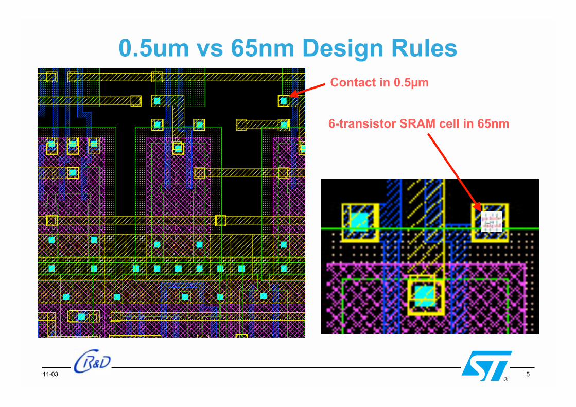
®11-03 5
0.5um vs 65nm Design RulesContact in 0.5µm
6-transistor SRAM cell in 65nm

®11-03 6
CMOS Roadmap: from R&D to production
2001 2002 2003 2004 2005 2006 2007
1st silicon
Protos acceptance
Production start
CMOS 45 nm
Advanced R&D
CMOS 32 nm
Advanced R&D
CMOS 90 nm
CMOS 65 nm
Advanced R&D
CMOS 120 nm
More than 4 generations in parallel

®11-03 7
45nm gate for GP device without Offset spacers45nm gate for GP device without Offset spacers
~35nm
Courtesy of F. Arnaud

®11-03 8
2 opposite requirements for the future
Increase processing power (GOPS):– Video, Audio, Graphics, Communications:
� High performance dedicated processors� A lot of embedded memories
– Replace Analog by Digital (e.g. digital Radio)
Reduce power consumption (Watt/Op):– Dynamic power = CV2f
� C: Need SOI-like junctions and LowK dielectrics� V: decrease VDD to the minimum to achieve Frequency f� F: keep Frequency pretty low, use parallelism
– Static power = as low as possible
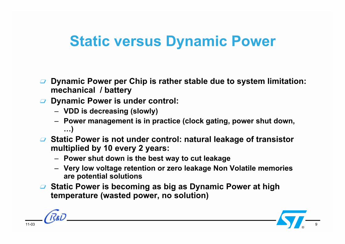
®11-03 9
Static versus Dynamic Power
Dynamic Power per Chip is rather stable due to system limitation:mechanical / batteryDynamic Power is under control:– VDD is decreasing (slowly)– Power management is in practice (clock gating, power shut down,
…)
Static Power is not under control: natural leakage of transistormultiplied by 10 every 2 years:– Power shut down is the best way to cut leakage– Very low voltage retention or zero leakage Non Volatile memories
are potential solutions
Static Power is becoming as big as Dynamic Power at hightemperature (wasted power, no solution)

®11-03 10
1
10
100
1000
10000
100000
300 400 500 600 700 800
Ion (µA/µm)
Ioff
(pA
/µm
)
H6H7
H8D
H10GP
H9GP
H9LP
Nmos Ion/Ioff evolution

®11-03 11
SoC Frequency & Leakage evolutionfrom 250nm to 90nm
0
100
200
300
400
500
600
700
H7A-1.8
VH7
A-2.5
VH7
-1.8V
H8D-65A-1.8
V
H8D-65A-2.5
VH7
-2.5V
H9LP
-ULL-1.2V
H9LP
-ULL-1.4V
H9-65A
-1.8V
H8D-LL-1.4V
H10LP-HV
T-1.0
V
H9GP
-ULL-1.0V
H9-65A
-3.3V
H8D-LL-1.8V
H9-65A
-3.6V
H9-65A
-2.5V
H9GP
-ULL-1.2V
H9-36A
-1.8V
H10LP-HV
T-1.2
V
H10L
P-SV
T-1.0
V
H8D-HS
-1.4V
H9GP
-LL-1.0
V
H10L
P-SV
T-1.2
V
H9GP
-LL-1.2
V
H8D-HS
-1.8V
H9LP
-HS-1.0
V
H9LP
-HS-1.2
V
H9LP
-HS-1.4
V
H9GP
-HS-1.0
V
H9GP
-HS-1.2
V
technology
freq
(M
Hz)
0.10
1.00
10.00
100.00
1000.00
10000.00
leak
age
(µA
/Kg
ate)
Frequency leakage/Kgate

®11-03 12
Low-Powertechniques for
wireless
Two supply zones: Vdd andVddSleep.Specific rules at RTL forboundary between Vdd andVddSleep areasGnd is common for all cells.Pads are always powered.3 power pads with embeddedswitches
Power-up control
Vdd Sleep
Vdd
Core power pads withswitches
Vddfillercut
Io pad supply
Vdd Sleep pad zone
®11-03 13
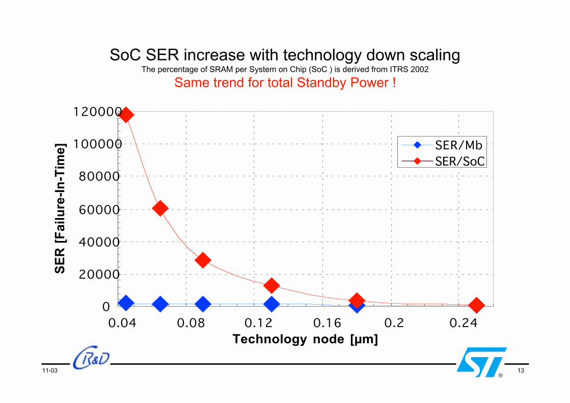
SoC SER increase with technology down scalingThe percentage of SRAM per System on Chip (SoC ) is derived from ITRS 2002
Same trend for total Standby Power !
0
20000
40000
60000
80000
100000
120000
0.04 0.08 0.12 0.16 0.2 0.24Technology node [µm]
SE
R [
Fai
lure
-In
-Tim
e] SER/Mb
SER/SoC

®11-03 14
Agenda
Technology Evolution
New system requirements
Hardware/Software co-design
Design Complexity and manufacturing costs
Concurrent hard/software design and validation
Flexible and Reconfigurable SoC
Conclusion

®11-03 15
Power Density in Microprocessors
i386i486
Pentium
Pentium II
Nuclear Reactor
Pentium IVPentium III
Pentium Pro
1
10
100
1000
i386 i486 Pentium Pentium Pro Pentium II Pentium III Pentium IV NuclearReactor
W/c
m2
i386i486
Pentium
Pentium II
Nuclear Reactor
Pentium IVPentium III
Pentium Pro
1
10
100
1000
i386 i486 Pentium Pentium Pro Pentium II Pentium III Pentium IV NuclearReactor
W/c
m2
1.51.5µµ 11µµ .7.7µµ .5.5µµ .35.35µµ .25.25µµ .18.18µµ .035.035µµ
Hot PlateHot Plate
Fred Pollack, IntelFred Pollack, Intel

®11-03 16
Required Performance for Multi-Media Processing (source ITRS Design ITWG July 2003)
GOPS
0.01 0.1 1 10
VideoVideo
AudioAudioVoiceVoice
CommunicationCommunicationRecognitionRecognition
GraphicsGraphics
FAXModem
2D Graphics
3D Graphics
MPEG
Dolby-AC3
JPEG
MPEG1Extraction
MPEG2 ExtractionMP/ML MP/HL
Compression
VoIP Modem
Word Recognition
Sentence Translation
GOPS: Giga Operations Per Second
100
Voice Auto Translation
10Mpps 100Mpps
MPEG4
Face Recognition
Voice Print Recognition
SW Defined Radio
Moving Picture Recognition

®11-03 17
PDA Model Characteristics(source ITRS Design ITWG July 2003)
Process Technology (nm) 130 9 0 6 5 4 5 3 2 2 2Operation Voltage (V) 1.2 1 0.8 0.6 0.5 0.4
Clock Frequency (MHz) 150 300 450 600 900 1200Application Real Time Video Codec Real Time Interpretation
(MAX performance required) (MPEG4/CIF)Application Web Browser TV Telephone (1:1) TV Telephone (>3:1)
(Others) Electric Mailer Voice Recognition (Input) Voice Recognition (Operation)Scheduler Authentication (Crypto Engine)
Processing Performance (GOPS) 0.3 2 1 4 7 7 461 2458Parallelism Factor 1 4 4 4 4 4
Communication Speed (Kbps) 6 4 384 2304 13824 82944 497664Power Consumption (MOPS/mW) 3 2 0 140 770 4160 24580
Peak Power Consumption (mW)(Requirement)
Battery Wh/Kg 120 200 400
2 2 2Standby power consumption (mW) (Requirement)
2 2 2
100 100 100
Still Image
Processing
100 100 100

®11-03 18
An Example of SoC for PDA (source ITRS Design ITWG July 2003)
0.18um/400MHz/470mW (typ)
CPU
I-cache32KB
D-cache32KB
I2C
FICP
USB
MMC
UART AC97
I2S
OST
GPIO
SSP
PWM RTC
DMA cnt.
LCDCnt.
MEMCnt.
PWR CPG
SDRAM64MB
Flash32MB
LCDPeripheral Area4 – 48MHz
Data Transfer Area
100MHz
Processor Area
Max 400MHz
-MM Application MP3 JPEG Simple Moving Picture
6.5MTrs.
-Available Time 6-10Hr
Specification
USB if
MMC
KEY
Sound

®11-03 19
An Example of SoC for Mobile Phone (source ITRS Design ITWG July 2003)
CPU
Cache32KB
XYRAM16KB
CPG
WDT
CMT
KEYIF
MMC
FLC
SIOF
SCIF
VIF
DMACMFIMEMCnt.
RAM ROM LCD
DSP
URAM128KB
-MM Function MP3 JPEG MPEG4 Java
-Talk Time 140min.-Standby Time 200Hr
RAM
CMOS camera
Bluetooth
Sound
NAND/ANDFlash
MMC
KEY
Peripheral Area 33MHz0.18um/133MHz/170mW (typ)
13.4Mtr (Including SRAM:9.5Mtr)
Processor Area133MHz
Flash
RF
BasebandSoC
RAM
ROM
Flash
Data TransferArea 66MHz
Specification

®11-03 20
SoC at the heart of conflicting trends
ST20ST20
MPEG2MPEG2VideoVideo
DolbyDolbyAC3AC3
FEIFEI
LinkLink
2 x 3 DAC2 x 3 DAC
Den
cD
enc
Time-to-market:Time-to-market:
Process roadmap
acceleration
Consumerization
of electronic devices
Process roadmap
acceleration
Consumerization
of electronic devices
Deep sub micron effects:Deep sub micron effects:
crosstalk
electro migration
wire delays, on-chip-variation
mask costs (OPC, PSM)
copper wires
crosstalk
electro migration
wire delays, on-chip-variation
mask costs (OPC, PSM)
copper wires
Complex systems:Complex systems:
uCs, DSPs HW/SW
SW protocol stacks
RTOS’s
Digital/Analog IPs
On-Chip busses
Process optionsexplosion (analog,RF, imagers, …)
uCs, DSPs HW/SW
SW protocol stacks
RTOS’s
Digital/Analog IPs
On-Chip busses
Process optionsexplosion (analog,RF, imagers, …)

®11-03 21
Agenda
Technology Evolution
New system requirements
Hardware/Software co-design
Design Complexity and manufacturing costs
Concurrent hard/software design and validation
Flexible and Reconfigurable SoC
Conclusion

®11-03 22
SoC Design + Rising Complexity =New Challenges
* Architecture effort overtakes physical design at 90nm
* Software costs overtake total hardware costs at 130nm
IBS Nov 2002

®11-03 23
PROBABILITY OF DESIGNS OPERATING AS EXPECTED
0
20
40
60
80
100
0.35µm 0.25µm 0.18µm 0.13µm 90nm
Pro
babi
lity
(%) Designs Operating as
Expected
Designs Requiring FullReticle Set
IBS Nov 2002

®11-03 24
Key Trends: ASICs down,Multi-processors & FPGAs up
ASIC/ASSP ratio: 80/20 in 2000, 50/50 in 2003Telecom company trends– In-house ASIC design way down– Replace by commercial off-the-shelf, programmable ASSP– High-end NPU’s used in non-NPU applications
Number of embedded processors in SoC rising:– ST: recordable DVD 5– Hughes: set-top box 7– ST: HDTV platform 8– Latest mobile handsets 10– NEC: Image processor 128– In-house NPU >150

®11-03 25
Key Trends: Embedded S/W contentin SoC is way up
eS/W: Current application complexity– Set-top box: >1 million lines of code– Digital audio processing: >1 million lines of code– Recordable DVD: Over 100 person-years effort– Hard-disk drive: eS/W represents 100 person-years effort
In multimedia systems– S/W cost (licenses, royalties) 6X larger than H/W chip cost– eS/W uses 50% to 80% of design resources
eS/W has become an essential part of SoC productsSoftware reuse essential nowSoftware architecture becoming importantMemory now dominating die area

®11-03 26
1
1010
1012
104
106
108
102
19701960 1980 20001990 2010 2020
Gates/chip: 2x / 18 monthseSW/chip: 2x / 10 monthseSW productivity: 2x / 5 years
Lines of code
H/W: +50% / year
eS/W
: +14
0% / y
ear
Gates
S/W and H/W Complexity Factors

®11-03 27
Agenda
Technology Evolution
New system requirements
Hardware/Software co-design
Design Complexity and manufacturing costs
Concurrent hard/software design and validation
Flexible and Reconfigurable SoC
Conclusion

®11-03 28
SoC Economic Trends: Mask NRE
– For $5 ASP with 25% profit margin:Need to sell over 1.6M parts to break even
Source: Dataquest
®11-03 29
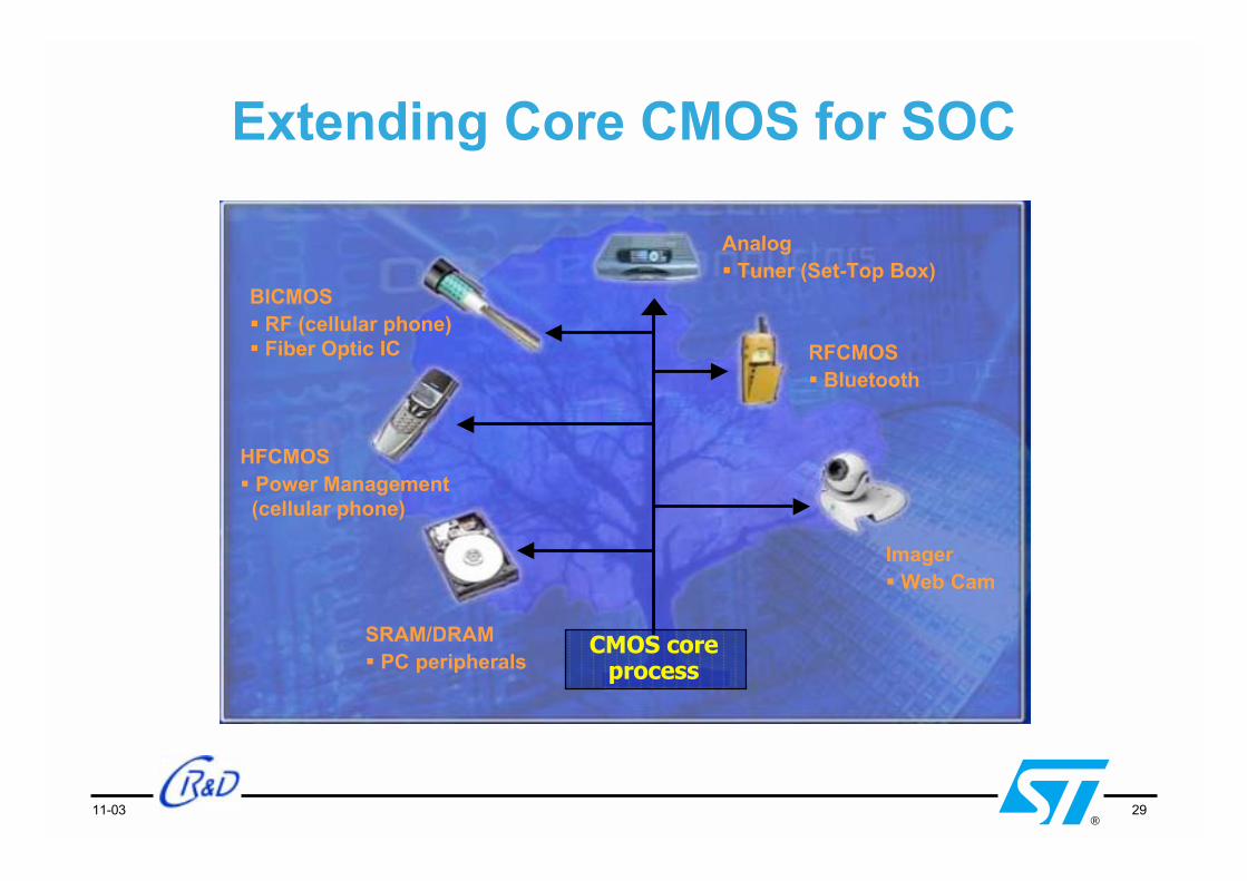
Extending Core CMOS for SOC
CMOS coreprocess
BICMOS� RF (cellular phone)� Fiber Optic IC
HFCMOS� Power Management (cellular phone)
SRAM/DRAM� PC peripherals
Analog� Tuner (Set-Top Box)
RFCMOS� Bluetooth
Imager� Web Cam

®11-03 30
Deep Submicrons Effectsmodeled in 0.13um
Voltage Drop& EMG
Copper RoutingCross Talkeffects
Substrate Noise

®11-03 31
New Timing Effects (90nm)
Sources: Motorola, University of Illinois, and Silicon Metrics
Temperature Map
30° C change →7% change in delay & slew
Slew
Temperature
Voltage on-chip-variations
5% voltage change →15% change in slew
Slew
Voltage
50% density change →15% change in slew
Transistor Density
Slew
Transistor Density

®11-03 32
Design For Test
1000
0.001
100000
1981 1995 2009
Log
ic T
ran
sist
ors
per
Ch
ip (
M)
Log
ic T
ran
sist
ors
per
Ch
ip (
M)
CAGR 58%
0.01
Pro
du
ctiv
ity
(K)T
ran
s./S
taff
-Mo
.P
rod
uct
ivit
y (K
)Tra
ns.
/Sta
ff-M
o.
CAGR 21% DFT
Memory generators: eSRAM, eDRAMeROM, eNVM– Include BIST generation
– Redundancy mandatory above 1Mbit
Logic– Scan / ATPG today
– Commercial tools to reduce test times by10X
– Implementing IEEE P1500 for core-basedtest
Design-for-Manufacturing– Yield-improving design guidelines under
definition

®11-03 33
Design For Manufacturability Gains
Reliabilityimprovement�
Acceleration forramp-up process(~months)
�
Yield gain formature process(3 to 5%)
�
Robustnessincrease(versus designmarginalities)
�
Standard approach
DFM approach
Process Maturity
Pro
du
cts
Yie
ld
�
�
®11-03 34
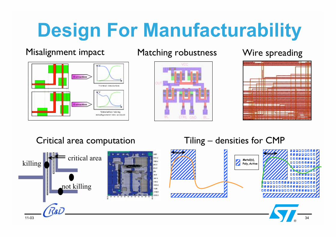
Design For Manufacturability
killing
not killing
critical area
Critical area computation
Metal(n),Poly,Active
100um 100um
Tiling – densities for CMP
Matching robustnessMisalignment impact Wire spreading

®11-03 35
SoC’s with CMOS-Imager process
� For mobile phone applications:� ZS450: CIF format (~100000 pixels)
� For webcam applications:� ZS422: QVGA format (~75000 pixels)
=> audio/video/video processing (SOC)
Area24.0 mm_
Area39.6 mm_
Area24.1 mm_
� ZS550: VGA format (~300000 pixels)

®11-03 36
Production 0.18um SoC’swith eDRAM
High-End Printer
Includes ARM micro
Low-End Printer(34 mm_)(20mm_)
4 Mbits eDRAM
6 Mbits eDRAM
DVD recorderDisk Controller(26 mm_) (34 mm_)
4 Mbits
eDRAM
Camera for
cell phone(15 mm_)
3 Mbits eDRAM
Includes Super10 microIncludes ST10 micro
Includes ARM micro

®11-03 37
IP & design validation effortcase study – 90nm test masks
� ASIC prototype� 30 Mtrans� SRAMs/ROM, PLL, IOs� Std cells IPs
� ROM compiler validation� SRAM compilers� SRAM bitcells qualification
� 17.5 Mbits
� Analog/RF IPs� IOs & fuse prototypes
� eDRAM macrocell� 12 Mbits

®11-03 38
Emb.memory offering expanding
spuhs
dphddphd
starsplpstarsplp
dpreg
spcacheNo cacheCache (data and tag)
bcam, tcambcam, tcamCAM
multiportmpaMulti port
spsmallspsmall
Register files
dprfdprf
romclpromv
romvrom
dplp
splpLow Power
splargesplargeHigh capacity
dphsdphs
sphssphs
High speed
spuhdspuhd
sphdsphd
High density
90nm0.13um
Partners
ST

®11-03 39
Agenda
Technology Evolution
New system requirements
Hardware/Software co-design
Design Complexity and manufacturing costs
Concurrent hard/software design and validation
Flexible and Reconfigurable SoC
Conclusion

®11-03 40
Concurrent Hardware/Software Design
� Standard Flow
Spec Archi Design Fab Breadboard Softwaredevelopment
SystemIntegration
SystemValidation
Time
GAINSystem
Validation
Softwaredevelopment
� Methodology Extensions
SystemIntegration

®11-03 41
Embedded Software Development Requires asMuch/More Design Effort Than Hardware

®11-03 42
Operating-System is bootingon simulated Cellphone (RTL)
CPU
Memory
DMA
HW1
HW2
PeripheralsRTL simulation
SoftwareReal RTOS
(Symbian)
ProcessorISS simu
HW-SW Co-simulationCycle-Accurate200 instr / sec

®11-03 43
ST40
ST20
TLM models - Fast SoC simulations
CPU
Memory
DMA
HW1
HW2
ProcessorISS simu
HW-SW Co-simulationTransaction-Accurate200 K+ instr / sec
Real embedded SoftwareApplication & Functional Verification
PeripheralsTLM simu
Standardizationbeing proposed toSystemC OSCI by ST,Cadence, ARM

®11-03 44
Platform-based design flow
BE cockpit
FE cockpit
Hardware
FE
BE
Appli
eSoftware
RTOS
DevDriversTests
TLM
TTLM
BCA
RTL
RTL
Gate
Layout
Technology independent
Technology dependent
Tests
IP meta-desc
IP views
IP library
XML Schema API for Intf + params
XML MetadataConsortiumformed with ST,Philips, ARM,Mentor, SNPS,CDS

®11-03 45
HW Emulation for MMC
CELARO
RTL Design
MMCI/F
FLASHI/F µ8051
MUX
AnalogBlocks
To MMChost
ToFLASH
RTL Design
MMCI/FMMCI/F
FLASHI/F
FLASHI/F µ8051µ8051
MUXMUX
AnalogBlocksAnalogBlocks
To MMChost
ToFLASH
• 1w setup-time• ~0.5MHz
• Real M58LW128FLASH chip in-circuit
• SW host running @100KHz• Connection of HW host ongoing

®11-03 46
First Prototype Platform: Aptix
ST120 Module
ARM7 Module
Virtex FPGA(GSM/GPRS modem)
Memory boards
Interface toRF/Tester

®11-03 47
HW/SW fast prototype platform
Faithful representation of the final design
Available much sooner than the final silicon
Guaranties the real-time behavior
Validation of the fundamentals of the SoC HW/SWarchitecture

®11-03 48
FPGA-based Prototyping Environment
RF GSM/GPRS Board
JTAG Connection toSW Debuggers
STEP1 BaseBandBoard

®11-03 49
IP Reuse Program� Organization
� company program “Design Methodology & IP Reuse”, CEO sponsored� corporate driven CR&D + cross-divisional Committee� domain-specific Work Groups RTL2Layout, AMS, SLD, DFT, Functional Verif., Power, …� intranet information site CAD On Line portal > K9 IP Reuse Pages
� Reuse standards� adherence to industry approach VSIA; RMM; Quality� deliverables / views BlueBook + Unicad Extension� IP packaging bbview (mapping from BB logic views to IP physical files)� HDL coding style Design Conventions + HAL associated checking tool� On Chip Bus VCI-close STBus; AMBA
� Methodology� Development flow Synopsys based Quartet� OCB support STBus, AMBA Platform kits� System Level SL model deliverables (TLM, BCA…)� Verification dynamic, formal, H/W-S/W, integration
� Infrastructure� Design Data Managt., Bug tracking Products from Synchronicity, Rational� IP Quality (IP=Product) IPScreen Certification; LibYield Maturity tracking� IP Procurement IP On Line catalog; Procurement, Exchange procedures

®11-03 50
IP certificationUSB2.0 example
If you pass OK, you have the logo
ST USB2 PHY

®11-03 51
NortelNortelNokiaNokia
AlcatelAlcatelSynopsysSynopsys
VirageVirage
IP IP ExternalExternalProviderProvider
ARMARM
IPIPDeliveryDelivery
Corporate IP Catalog Project
IP IP InternalInternalProviderProvider
IP IP InternalInternalDeliveryDelivery

®11-03 52
Multi-Site Collaborative Design(Synchronicity-based)
Memory Random Logic
CPU PCI
Graphics
Multiple DesignersMultiple DesignersMultiple LocationsMultiple Locations
One ChipOne Chip


![Designingenergyefficient’ microprocessor:Howtofight ... Memory ... [MHz] 8086 80286 386DX 486DX 486DX4 Pentium Pentium Pro Pentium II Pentium MMX Pentium III ... Delay buffers are](https://img.pdfslide.net/doc/110x75/5ac1a5637f8b9ac6688d9ef1/designingenergyecient-microprocessorhowtoght-memory-mhz-8086.jpg)