Embed Size (px)
Citation preview

APPLICATION NOTE
R01AN1710EJ0100 Rev. 1.00 Page 1 of 60 Sep. 16, 2014
RX63N Group, RX631 Group Flash Bootloader with the USB Peripheral CDC
Abstract This application note describes a method to reprogram the on-chip flash memory via USB memory (flash bootloader via USB) using the USB 2.0 host/function module as a function controller.
The features of the flash bootloader via USB are described below.
Controls the target device by transmitting commands from a PC. With commands from a PC, erasing, programming, blank checking, or target program execution are performed for the flash memory on the target device.
Programs in the Motorola S format can be programmed. Supports USB 2.0 full-speed transfer. Compliant with the Abstract Control Model in the Universal Serial Bus Class Definitions for Communications
Devices.
Products - RX63N Group 177-pin and 176-pin packages with a ROM size between 768 KB and 2 MB
- RX63N Group 145-pin and 144-pin packages with a ROM size between 768 KB and 2 MB
- RX63N Group 100-pin package with a ROM size between 768 KB and 2 MB
- RX631 Group 177-pin and 176-pin packages with a ROM size between 256 KB and 2 MB
- RX631 Group 145-pin and 144-pin packages with a ROM size between 256 KB and 2 MB
- RX631 Group 100-pin package with a ROM size between 256 KB and 2 MB
When using this application note with other Renesas MCUs, careful evaluation is recommended after making modifications to comply with the alternate MCU.
R01AN1710EJ0100 Rev. 1.00
Sep. 16, 2014

RX63N Group, RX631 Group Flash Bootloader with the USB Peripheral CDC
R01AN1710EJ0100 Rev. 1.00 Page 2 of 60 Sep. 16, 2014
Contents
1. Specifications ..................................................................................................................................... 4
2. Operation Confirmation Conditions .................................................................................................... 5
3. Reference Application Notes .............................................................................................................. 6
4. Hardware ............................................................................................................................................ 6 4.1 Pins Used ..................................................................................................................................... 6
5. Software ............................................................................................................................................. 7 5.1 Operation Overview ..................................................................................................................... 7 5.2 Commands ................................................................................................................................... 9 5.3 Start Address of the Target Program ........................................................................................... 9 5.4 Mode Transitions ....................................................................................................................... 10
5.4.1 Idle Mode ............................................................................................................................ 10 5.4.2 Command display Mode ..................................................................................................... 10 5.4.3 Command Wait Mode ......................................................................................................... 10 5.4.4 Blank Check Mode .............................................................................................................. 10 5.4.5 Erase Mode ........................................................................................................................ 10 5.4.6 Program Mode .................................................................................................................... 11 5.4.7 Error End Wait Mode .......................................................................................................... 11 5.4.8 Program Execution Mode ................................................................................................... 11
5.5 Data Flow when Programming ................................................................................................... 12 5.6 ROM Capacity ............................................................................................................................ 13 5.7 File Composition ........................................................................................................................ 14 5.8 Constants ................................................................................................................................... 15 5.9 Structure/Union List ................................................................................................................... 16 5.10 Message Table List .................................................................................................................... 17 5.11 Functions .................................................................................................................................... 18 5.12 Function Specifications .............................................................................................................. 19 5.13 Flowcharts .................................................................................................................................. 28
5.13.1 USB Main Processing ........................................................................................................ 28 5.13.2 Reprogramming Main Processing ..................................................................................... 30 5.13.3 Processing During Idle Mode ............................................................................................ 31 5.13.4 Command Analysis ............................................................................................................ 32 5.13.5 Erase Processing .............................................................................................................. 33 5.13.6 Program Processing .......................................................................................................... 33 5.13.7 Executing the Target Program .......................................................................................... 34 5.13.8 Wait for Completion of an Error Processing ...................................................................... 35 5.13.9 Displaying Commands ....................................................................................................... 36 5.13.10 Start Processing for Blank Check .................................................................................... 36 5.13.11 Start Processing for Erasing ............................................................................................ 36 5.13.12 Start Processing for Programming .................................................................................. 37 5.13.13 Executing the Target Program ........................................................................................ 37 5.13.14 Blank Check .................................................................................................................... 38 5.13.15 Erasing the Target Area .................................................................................................. 39

RX63N Group, RX631 Group Flash Bootloader with the USB Peripheral CDC
R01AN1710EJ0100 Rev. 1.00 Page 3 of 60 Sep. 16, 2014
5.13.16 Storing Motorola S Format Data ...................................................................................... 40 5.13.17 Motorola S Format Header Analysis and Binary Data Conversion ................................. 41 5.13.18 ASCII to Binary Conversion of Motorola S Format Data ................................................. 43 5.13.19 Making Programming Data .............................................................................................. 44 5.13.20 Programming the Target Area ......................................................................................... 45 5.13.21 Clearing Variables for Motorola S Format Data .............................................................. 46 5.13.22 Stopping USB .................................................................................................................. 47 5.13.23 Storing USB Receive Data .............................................................................................. 48 5.13.24 Storing USB Transmit Data ............................................................................................. 48 5.13.25 Setting Message Data to be Displayed ........................................................................... 49 5.13.26 Checking Receive Ring Buffer Space ............................................................................. 50 5.13.27 Checking Data in the Transmit Ring Buffer ..................................................................... 50 5.13.28 Executing the Target Program with the USB Disconnected............................................ 51 5.13.29 Storing Data in the Receive Ring Buffer.......................................................................... 51 5.13.30 Reading the Receive Ring Buffer .................................................................................... 52 5.13.31 Clearing the Receive Ring Buffer .................................................................................... 52 5.13.32 Checking the Number of Data in the Receive Ring Buffer .............................................. 52 5.13.33 Storing Data in the Transmit Ring Buffer......................................................................... 53 5.13.34 Reading the Transmit Ring Buffer ................................................................................... 53 5.13.35 Clearing the Transmit Ring Buffer ................................................................................... 53 5.13.36 Checking the Number of Data in the Transmit Ring Buffer ............................................. 54 5.13.37 ASCII to Binary Conversion ............................................................................................. 54
6. Using the Sample Code ................................................................................................................... 55
7. Sample Target Program ................................................................................................................... 56
8. Notes on Using This Application Note .............................................................................................. 56 8.1 Programming Speed .................................................................................................................. 56 8.2 USB Disconnection During Programming or Erasing ................................................................ 56 8.3 HEW Configuration .................................................................................................................... 56 8.4 Vender ID and Product ID for the USB ...................................................................................... 56 8.5 Interrupts in the Fixed Vector Table ........................................................................................... 56 8.6 Reset Vector of the Target Program .......................................................................................... 56 8.7 Motorola S Format ..................................................................................................................... 56 8.8 Processing with the while(1) Statement ..................................................................................... 56 8.9 Stop of the Program During USB Communication..................................................................... 56 8.10 Endian ........................................................................................................................................ 56 8.11 Changes in the Simple Flash API for RX ................................................................................... 57 8.12 Changes in the USB PCDC Driver ............................................................................................ 58
8.12.1 Changed Items .................................................................................................................. 58 8.12.2 Additional Files .................................................................................................................. 58 8.12.3 Additional Sections ............................................................................................................ 58 8.12.4 Include File Directory ......................................................................................................... 59 8.12.5 Linker Settings ................................................................................................................... 59
8.13 Changes in the RX63N Group, RX631 Group Initial Setting ..................................................... 59
9. Sample Code .................................................................................................................................... 60
10. Reference Documents ...................................................................................................................... 60

RX63N Group, RX631 Group Flash Bootloader with the USB Peripheral CDC
R01AN1710EJ0100 Rev. 1.00 Page 4 of 60 Sep. 16, 2014
1. Specifications With the flash bootloader via USB, commands are transmitted from the terminal application on the host PC to the MCU to reprogram the flash memory on the MCU.
Table 1.1 lists the Peripheral Functions and Their Applications and Figure 1.1 shows a Usage Example.
Table 1.1 Peripheral Functions and Their Applications
Peripheral Function Application
ROM (flash memory for code storage) Reprogramming the on-chip flash memory in ROM P/E mode.
USB 2.0 host/function module Communication with the host PC.
On-chip flash memory
Reprogram in P/E mode
MCU(RX63N, RX631)
Terminal application(command transmission)
USB interface
Target board
Figure 1.1 Usage Example

RX63N Group, RX631 Group Flash Bootloader with the USB Peripheral CDC
R01AN1710EJ0100 Rev. 1.00 Page 5 of 60 Sep. 16, 2014
2. Operation Confirmation Conditions The sample code accompanying this application note has been run and confirmed under the conditions below.
Table 2.1 Operation Confirmation Conditions
Item Contents MCU used R5F563NBDDFC (RX63N Group)
Operating frequencies
- Main clock: 12 MHz - PLL: 192 MHz (main clock divided by 1 and multiplied by 16) - System clock (ICLK): 96 MHz (PLL divided by 2) - FlashIF clock (FCLK): 48 MHz (PLL divided by 4) - External bus clock (BCLK): 24 MHz (PLL divided by 8) - Peripheral module clock B (PCLKB): 48 MHz (PLL divided by 4) - USB clock (UCLK): 48 MHz (PLL divided by 4)
Operating voltage 3.3 V Integrated development environment
Renesas Electronics Corporation High-performance Embedded Workshop Version 4.09.01
C compiler
Renesas Electronics Corporation C/C++ Compiler Package for RX Family V.1.02 Release 01
Compile options --cpu=rx600 -bit_order=left -include="$(WORKSPDIR)\WorkSpace\ANSI" -include="$(WORKSPDIR)\WorkSpace\CDCFW\include" -include="$(WORKSPDIR)\WorkSpace\HwResourceForUSB\inc" -include="$(WORKSPDIR)\WorkSpace\HwResourceForUSB\USBHW" -include="$(WORKSPDIR)\WorkSpace\HwResourceForUSB\USBHW\DEF" -include="$(WORKSPDIR)\WorkSpace\HwResourceForUSB\USBHW\REG" -include="$(WORKSPDIR)\WorkSpace\HwResourceForUSB\USRCFG" -include="$(WORKSPDIR)\WorkSpace\SmplMain\APL" -include="$(WORKSPDIR)\WorkSpace\USBSTDFW\include" -include="$(WORKSPDIR)\WorkSpace\FLASH" -include="$(WORKSPDIR)\WorkSpace\FLASH\src" -include="$(WORKSPDIR)\WorkSpace\r_bsp" -define=USB_FW_PP=USB_FW_NONOS_PP,USBC_DEBUGLCD_PP -output=obj="$(CONFIGDIR)\$(FILELEAF).obj" -debug -nostuff -nologo
iodefine.h version Version 1.6A Endian Little endian Operating mode Single-chip mode Processor mode Supervisor mode Sample code version Version 1.00 Board used Renesas Starter Kit+ for RX63N (product part no.: R0K50563NC000BE)

RX63N Group, RX631 Group Flash Bootloader with the USB Peripheral CDC
R01AN1710EJ0100 Rev. 1.00 Page 6 of 60 Sep. 16, 2014
3. Reference Application Notes For additional information associated with this document, refer to the following application notes.
- RX600 & RX200 Series Simple Flash API for RX Rev.2.40 (R01AN0544EU) - Renesas USB MCU and USB ASSP USB Basic Host and Peripheral firmware Rev.2.10 (R01AN0512EJ) - Renesas USB MCU and USB ASSP USB Peripheral Communications Device Class Driver (PCDC) Rev.2.10
(R01AN0273EJ) - RX63N Group, RX631 Group Initial Setting Rev. 1.10 (R01AN1245EJ)
The functions in the reference application notes above are used in the sample code in this application note. The revision number of the reference application note is current as of when this application note was made. However the latest version is always recommended. Visit the Renesas Electronics Corporation website to check and download the latest version.
4. Hardware
4.1 Pins Used Table 4.1 lists the Pins Used and Their Functions.
Table 4.1 Pins Used and Their Functions
Pin Name I/O Function
USB1_DP I/O D+ I/O pin of the USB on-chip transceiver Connected to the D+ pin of the USB bus.
USB1_DM I/O D- I/O pin of the USB on-chip transceiver Connected to the D- pin of the USB bus.
USB1_VBUS Input USB cable connection monitor pin Connected to VBUS of the USB bus. The state of the VBUS connection (connected/disconnected) can be detected.
USB1_DPUPE Output 1.5-kΩ pull-up resistor control signal for USB D+ signal Note: • For settings of the other pins used in the USB Peripheral Communication Device Class Driver (USB
PCDC driver) such as switch or SCI, refer to the USB Peripheral Communications Device Class Driver (PCDC) application note.

RX63N Group, RX631 Group Flash Bootloader with the USB Peripheral CDC
R01AN1710EJ0100 Rev. 1.00 Page 7 of 60 Sep. 16, 2014
5. Software
5.1 Operation Overview The sample code receives command data from the host PC and performs the operation (command display, blank check, erase, program, or target program execution) according to the command. Commands from the host PC are transmitted by the terminal application. The sample code can reprogram only the specific part (target area) of the user area. Addresses FFFF0000h to FFFFFFFFh are used by the sample code itself and cannot be reprogrammed.
Figure 5.1 shows the Memory Allocation.
Target area (ROM) (2)
(user can use this area)
ROM used by the sample code
0000 0000h
0002 0000h
FFFF FFFFh
FFFE 0000h
FFF0 0000h
When R5F563NBDDFC is used:(ROM: 1 MB, RAM: 128 KB)
RAM (user can use this area)
Reserved area, peripheral I/O register,
etc.
On-chip ROM
RAM used by the sample code (1)
On-chip RAM
Notes: 1. This area can be used by the user while the target program is being executed.2. The target program is written to this area.
Figure 5.1 Memory Allocation

RX63N Group, RX631 Group Flash Bootloader with the USB Peripheral CDC
R01AN1710EJ0100 Rev. 1.00 Page 8 of 60 Sep. 16, 2014
In the sample code, the flash memory is reprogrammed in the following steps.
(1) After a reset, if the MCU is not connected to a PC and the value in the target reset vector (address FFFD FFFCh) is not FFFF FFFFh, the target program is executed. If connected to the PC, the MCU transmits the message "Press any key" to the PC at a certain intervals until the MCU receives a data (until the terminal application is started and a key is pressed on the keyboard). See Figure 5.2 below.
(2) When the MCU receives data from the PC, it transmits the command list to the PC and waits for receiving a command data. See Figure 5.3 below.
(3) When a command is received, the MCU performs the operation (command display, blank check, erase, program, or target program execution) according to the command.
Press any key.
Press any key.
Terminal Application
Figure 5.2 Screen Example When Waiting for Key Input
Press any key.
Press any key.
Renesas USB Flash SamplePress:- 1 - Show instructions(these). 2 - Blank check. 3 - Erase target area. 4 - Start programming. 5 - Run target program.
Terminal Application
Figure 5.3 Screen Example for Inputting a Command

RX63N Group, RX631 Group Flash Bootloader with the USB Peripheral CDC
R01AN1710EJ0100 Rev. 1.00 Page 9 of 60 Sep. 16, 2014
5.2 Commands Table 5.1 lists the Commands. The commands are listed on the terminal application by the show instructions command.
Table 5.1 Commands
Key Entered on the PC ASCII Code Command 1 31h Show instructions(these) 2 32h Blank check 3 33h Erase target area. 4 34h Start programming 5 35h Run the target program
5.3 Start Address of the Target Program In the sample code, if the USB is not connected after a reset, or if the target program execution command is selected, the target program is executed. The target program is executed from the address written in address FFFD FFFCh (target reset vector). This means that the reset vector of the target program should be FFFD FFFCh. Thus the start address of the target program needs to be stored in the target reset vector in advance.
Target area (ROM)(user can use this area)
ROM used by the sample code
FFFF FFFFh
FFFF 0000h
FFF0 0000h
FFFD FFFCh FFF0 0000h
The program is executed from the address written in address FFFD FFFCh (target reset vector)
Figure 5.4 Target Reset Vector

RX63N Group, RX631 Group Flash Bootloader with the USB Peripheral CDC
R01AN1710EJ0100 Rev. 1.00 Page 10 of 60 Sep. 16, 2014
5.4 Mode Transitions Figure 5.5 shows the Mode Transitions in the Sample Codes.
Idle
After a reset
Command wait
Program execution
Command display
Erase
Program
Blank check
USB connected and a key input
Command list displayed
Show instructions command
Error end wait
Run the target program command
Target reset vector: FFFF FFFFh
Command error No transmission
from the PC for a certain time
Error occurred
Blank check command
Erase target area command
Erase completed
Target program executed
Target reset vector is not FFFF FFFFh
Check completed
Programming completed
USB not connected and the target reset vector is
not FFFF FFFFh
Start programming
command
Figure 5.5 Mode Transitions in the Sample Codes
5.4.1 Idle Mode After a reset, the MCU enters idle mode. If the USB is not connected and the target reset vector has a value other than FFFF FFFFh, the target program is executed. If the USB is connected, the MCU transmits the message to prompt for key input at a certain intervals. When a key is pressed on the PC (i.e., when the MCU receives a given data), the MCU enters command display mode.
5.4.2 Command display Mode The command list is displayed. After the list is displayed, the MCU enters command wait mode.
5.4.3 Command Wait Mode The MCU waits for a command from the PC. When a command is received, the MCU enters a mode according to the command received.
5.4.4 Blank Check Mode The blank check is performed for the target area. When the blank check is completed, the blank check result is displayed and the MCU enters command wait mode.
5.4.5 Erase Mode The target area is erased using the Simple Flash API. When the erasing is completed, the erase result is displayed and the MCU enters command wait mode.

RX63N Group, RX631 Group Flash Bootloader with the USB Peripheral CDC
R01AN1710EJ0100 Rev. 1.00 Page 11 of 60 Sep. 16, 2014
5.4.6 Program Mode The target area is programmed using the Simple Flash API. After the MCU receives the start programming command, it waits for receiving a mot file. Send a mot file in ASCII from the PC. Operations after the MCU receives the command are as follows:
(1) The MCU waits for receiving 'S' (in ASCII) that is the first data of the Motorola S format. Any data other than 'S' is discarded.
(2) After receiving 'S', the MCU receives data in Motorola S format and programs the received data. Once 'S' is received, if the subsequent received data is not in Motorola S format, the MCU enters error end wait mode. It also enters error end wait mode if the other error occurs such as checksum. Refer to 5.10 “Message Table List” for details on errors and displayed messages.
(3) When the program operation is completed, a message to inform of the result is displayed. Then the MCU enters command wait mode.
Note: • Once data is determined as Motorola S format data, data through to checksum is recognized as Motorola S format in the sample code. The sample code discards data after checksum, which is received simultaneously. If the data which is supposed to be discarded is received after the actual discard operation, the MCU receives the data as a command. In this case the message for command error may be displayed.
5.4.7 Error End Wait Mode If the MCU receives a command not listed in 5.2 Commands, or if an error occurs in program mode, the MCU enters error end wait mode. If no data is received from the PC for a certain period during error end wait mode, the MCU enters command wait mode.
When there is an error in a received mot file, the MCU cancels the program operation while the terminal application may continue to transmit data. Then if the MCU enters command wait mode immediately after an error occurred, such transmit data may be received as a command. Therefore the MCU enters error end wait mode once and waits until no data is transmitted from the PC. Note that any data received from the PC during error end wait mode will be discarded.
5.4.8 Program Execution Mode The USB is stopped and the target program is executed. If the value of the target reset vector is FFFF FFFFh, an appropriate error message is displayed and the MCU enters command wait mode.

RX63N Group, RX631 Group Flash Bootloader with the USB Peripheral CDC
R01AN1710EJ0100 Rev. 1.00 Page 12 of 60 Sep. 16, 2014
5.5 Data Flow when Programming Figure 5.6 shows the flow of data within the MCU when programming the target area on the flash memory.
When receiving:
(1) Data received from the PC is transferred to the receive ring buffer.
(2) One record of Motorola S format data is copied to the MotS buffer (ASCII).
(3) The header part of the Motorola S format data is analyzed, and at the same time, ASCII data is converted to binary data and stored in the MotS buffer (binary).
(4) Data is stored in the programming buffer. Data is programmed in the user area of the MCU in 256 bytes. Steps (1) to (4) are repeated until the size of the stored programming data becomes 256 bytes. If the size exceeds 256 bytes, the excess data is temporarily stored and used when programming the next 256 bytes.
(5) The prepared data (256 bytes) is written to the flash memory using the Simple Flash API.
When transmitting:
(6) The result of the programming operation is determined by the return value from the Simple Flash API.
(7) The message corresponding to the result of the programming operation is stored in the transmit ring buffer.
(8) The message is transmitted to the PC using the USB PCDC driver.
Display message table
(Error, Completeand other
messages)
Receive data
US
B P
CD
C d
river
Receive ring buffer MotS buffer(ASCII)
Copies one record of MotS format data
MotS buffer(binary)
Analyzes the header and
converts data to binary
Programming buffer
Stores in the programming
buffer
RX
600
& R
X20
0 S
erie
s S
impl
e Fl
ash
AP
I for
RX
Programming data
(256 bytes)
Stores 256 bytes of programming data and calls the Simple Flash API.
Transmit ring bufferStores the message data in the transmit ring buffer
Notifies of the programming result (succeeded/failed)
Transmit data
Processing Performed by the Sample Code
(1) (2) (3) (4) (5)
(6)(7)(8)
Figure 5.6 Data Flow when Programming

RX63N Group, RX631 Group Flash Bootloader with the USB Peripheral CDC
R01AN1710EJ0100 Rev. 1.00 Page 13 of 60 Sep. 16, 2014
Figure 5.7 shows the Data Structures when Programming.
'S'
Receive ring bufferfl_ring_data
- Copies one record only.- Discards control codes.
(2)
n
Length 1
Length 2
Addr 1
Addr 2
Addr i
Data 1
Data 2
Data i
Sum 1
Sum 2
Control code
'S'
n
MotS buffer (ASCII)fl_wr_mot_s
'S'
n
Length 1
Length 2
Addr 0
Addr 1
Addr i
Data 1
Data 2
Data i
Sum 1
Sum 2
MotS buffer (binary)fl_wr_mot_s_bin
Length 1
Addr 1
Addr 2
Addr 4
Data 1
Data 2
Data i
(3)
Programming bufferfl_writing_data
Addr 1
Addr 2
Addr 4
Data 1
Data 2
Data 256
- Converts ASCII to binary.- Converts sizes of address and data length to 32 bits.- Calculates checksum.- If the record format is S3, discards the header ('S3'), and Sum 1 and Sum 2, and goes to (4).- If the record format is a format other than S3, discards all data.
(4)
- Stores data in the buffer (256-byte).- Discards the data length.
Temporary buffer (binary)fl_wr_mot_s_bin_surplus
Length 1
Addr 1
Addr 2
Addr 4
Data 1
Data 2
Data j
- If the total size of the current and previous programming data exceeds 256 bytes, stores the excess data temporarily.
Addr 3
Addr 3
Addr 3
Figure 5.7 Data Structures when Programming
5.6 ROM Capacity The sample code assumes 1 MB ROM is used. When an MCU with ROM capacity other than 1 MB is used, change the "FL_END_BLOCK_NUM" definition in the r_Flash_main.h file appropriate to the MCU used.
Table 5.2 lists the ROM Capacities of the Target Area.
Table 5.2 ROM Capacities of the Target Area
ROM Capacity ROM Capacity of the Target Area
Start Address of the Target Area
Block Number of the Target Area
2 MB 1920 KB FFE0 0000h EB14 to EB69 1.5 MB 1408 KB FFE8 0000h EB14 to EB61 1 MB 896 KB FFF0 0000h EB14 to EB53
768 KB 640 KB FFF4 0000h EB14 to EB45 512 KB 384 KB FFF8 0000h EB14 to EB37 384 KB 256 KB FFFA 0000h EB14 to EB29 256 KB 128 KB FFFC 0000h EB14 to EB21

RX63N Group, RX631 Group Flash Bootloader with the USB Peripheral CDC
R01AN1710EJ0100 Rev. 1.00 Page 14 of 60 Sep. 16, 2014
5.7 File Composition Table 5.3 lists the Files Used in the Sample Code.
Table 5.3 Files Used in the Sample Code
File Name Outline Remarks
r_flash_api_rx.c RX600 & RX200 Series Simple Flash API program for RX
Refer to the RX600 & RX200 Series Simple Flash API for RX application note for details.
r_flash_api_rx63n.h External reference header file for RX600 & RX200 Series Simple Flash API program for RX
r_flash_api_rx_private.h Header file for RX600 & RX200 Series Simple Flash API for RX.
r_flash_api_rx_config.h External reference header file for RX600 & RX200 Series Simple Flash API program for RX.
r_flash_api_rx_if.h External reference header file for RX600 & RX200 Series Simple Flash API program for RX.
r_init_stop_module.c Stop processing for active peripheral functions after a reset
r_init_stop_module.h Header file for r_init_stop_module.c r_init_non_existent_port.c Nonexistent port initialization r_init_non_existent_port.h Header file for r_init_non_existent_port.c r_init_clock.c Clock initialization r_init_clock.h Header file for r_init_clock.c r_Flash_main.c Flash reprogramming data processing
r_Flash_main.h External reference header file for flash reprogramming data processing
r_Flash_buff.c Processing associated with buffers used for USB transmission/reception
r_Flash_buff.h External reference header file for processing associated with buffers used for USB transmission/reception
TrgtPrgDmmy.c Dummy program for allocating space for the target program
Files in the r_bsp folder Programs in the r_bsp package used for RX600 & RX200 Series Simple Flash API program for RX
Other files Programs of the USB PCDC driver
Refer to the “USB Basic Host and Peripheral firmware” and “USB Peripheral Communications Device Class Driver” application notes for details.

RX63N Group, RX631 Group Flash Bootloader with the USB Peripheral CDC
R01AN1710EJ0100 Rev. 1.00 Page 15 of 60 Sep. 16, 2014
5.8 Constants Table 5.4 lists the Constants Used in the Sample Code. Note that constants used in the USB PCDC driver and Simple Flash API are not included here.
Table 5.4 Constants Used in the Sample Code
Constant Name Setting Value Contents FL_CMD_DATA_SHOW_INST 31h Command value that is 1 in ASCII FL_CMD_DATA_BLNK_CHECK 32h Command value that is 2 in ASCII FL_CMD_DATA_ERASE_TRGT_AREA 33h Command value that is 3 in ASCII FL_CMD_DATA_PRG_TRGT_AREA 34h Command value that is 4 in ASCII FL_CMD_DATA_RUN_TRGT_AREA 35h Command value that is 5 in ASCII
FL_RINGBUFF_SIZE 1024 Ring buffer size for receiving data from the USB
FL_RINGBUFF2_SIZE 256 Ring buffer size for transmitting data to the USB
FL_USB_RCV_BLANK_SIZE 64 The data size that the USB can transmit at a time.
FL_SEND_END_CODE 00h End code of the message table
FL_MOTS_ADDR_SIZE 4 Buffer size for the address of Motorola S format data
FL_MOTS_SUM_SIZE 1 Buffer size for the checksum of Motorola S format data
FL_START_BLOCK_NUM 14 First block of the target area FL_END_BLOCK_NUM 53 Last block of the target area FL_TARGET_REST_VECT_ADDR FFFD FFFCh Target reset vector
FL_USB_UNCONNECT_WAIT_PERIOD 10000h Wait time until the target program is executed with the USB disconnected
FL_IDLE_MESSAGE_OUTPUT_PERIOD 10000h Interval of time to display the message when in idle mode
FL_ERROR_WAIT_PERIOD 10000h Wait time for completion of an error (the wait processing is terminated if nothing is received from the USB during counting this value.)

RX63N Group, RX631 Group Flash Bootloader with the USB Peripheral CDC
R01AN1710EJ0100 Rev. 1.00 Page 16 of 60 Sep. 16, 2014
5.9 Structure/Union List Figure 5.8 shows the Structure/Union Used in the Sample Code. Note that structure/union used in the USB PCDC driver and Simple Flash API are not included here.
/* buffer for mot S format data */typedef struct uint8_t type[2]; /* "S0", "S1" and so on */ uint8_t len[2]; /* "0-255" */ uint8_t addr_data_sum[512]; Fl_prg_mot_s_t;
/* buffer for write data (this data is the converted data from mot S format data) */typedef struct uint8_t len; uint32_t addr; uint8_t data[256]; Fl_prg_mot_s_binary_t;
/* buffer for writing flash */typedef struct uint32_t addr; uint8_t data[256]; Fl_prg_writing_data_t;
Figure 5.8 Structure/Union Used in the Sample Code

RX63N Group, RX631 Group Flash Bootloader with the USB Peripheral CDC
R01AN1710EJ0100 Rev. 1.00 Page 17 of 60 Sep. 16, 2014
5.10 Message Table List Table 5.5 lists messages used in the sample code. The new line character is omitted from each message in the table.
Table 5.5 Messages Used in the Sample Code
Message Description Press any key. Displayed periodically in idle mode. Renesas USB Flash Sample Press:- 1 - Show instructions(these). 2 - Blank check. 3 - Erase target area. 4 - Start programming. 5 - Run target program.
Command list
Target area is blank. After a blank check, displayed when the target area is blank.
Target area is NOT blank. After a blank check, displayed when the target area is not blank.
Erase target area... Displayed when an erase operation is in progress. Erase complete. Displayed when an erase operation is completed. ERROR!!! - Erase is failed. Displayed when an erase operation is failed.
Please send a mot file. Displayed when a program operation is started. Send a mot file after this message is displayed.
Program complete. Displayed when a program operation is completed. Program failed. Displayed when a program operation is failed. ERROR!!! - Verify error. Displayed when a verify error occurred. Run target program. Displayed when the target program is executed. ERROR!!! - Target reset vector(0xFFFDFFFC) is 0xFFFFFFFF.
Displayed when the target vector is FFFF FFFFh in attempting to execute the target program.
ERROR!!! - Command error. Please press a number from 1 to 5. Displayed when an incorrect command is entered.
ERROR!!! - Mot file format is NOT correct. Displayed when an incorrect target program is transmitted.
ERROR!!! - Check sum error. Displayed when a checksum error occurred in Motorola S format in the target program.
Please wait for instructions to be shown.
Displayed when an error occurred and data continues to be transmitted. The MCU enters command wait mode when data is not transmitted for a certain period. If data continues to be sent after the error occurrence, a period (.) is displayed in regular intervals.
Period (.) Displayed in regular intervals after an error occurred. Newline code (\r\n) Used for a newline following each message.

RX63N Group, RX631 Group Flash Bootloader with the USB Peripheral CDC
R01AN1710EJ0100 Rev. 1.00 Page 18 of 60 Sep. 16, 2014
5.11 Functions Table 5.6 lists the Functions. Note that functions used in the USB PCDC driver and Simple Flash API are not included here.
Table 5.6 Functions
Function Name Outline R_INIT_StopModule Stop processing for active peripheral functions after a reset R_INIT_NonExistentPort Nonexistent port initialization R_INIT_Clock Clock initialization R_Fl_Rewrite_process Reprogramming main processing R_Fl_Idle Processing during idle mode (until a key is pressed after a reset) R_Fl_AnalyzeCMD Command analysis R_Fl_EraseTrgtArea Erase processing R_Fl_PrgTrgtArea Program processing R_Fl_RunTrgtPrg Executing the target program R_Fl_ErrorWait Wait for completion of an error processing R_Fl_cmd_ShowInst Displaying commands R_Fl_cmd_BlankCheckStart Start processing for blank check R_Fl_cmd_EraseStart Start processing for erasing R_Fl_cmd_PrgStart Start processing for programming R_Fl_cmd_RunTrgtPrgStart Executing the target program R_Fl_Blnk_BlankCheck Blank check R_Fl_Ers_EraseFlash Erasing the target area R_Fl_Prg_StoreMotS Storing Motorola S format data R_Fl_Prg_ProcessForMotS_data Motorola S format header analysis and binary data conversion R_Fl_Prg_MotS_AsciiToBinary ASCII to binary conversion of Motorola S format data R_Fl_Prg_MakeWriteData Making programming data R_Fl_Prg_WriteData Programming the target area R_Fl_Prg_ClearMotSVariables Clearing variables for Motorola S format data R_Fl_Run_StopUSB Stopping USB R_Fl_RcvDataString Storing USB receive data R_Fl_SetSendData Storing USB transmit data R_Fl_SetDisplayMsgData Setting message data to be displayed (dot display) R_Fl_RingCheckBlank Checking receive ring buffer space R_Fl_Ring2CheckData Checking data in the transmit ring buffer R_Fl_USB_NonConnect_Run Executing the target program with the USB disconnected R_Fl_RingEnQueue Storing data in the receive ring buffer R_Fl_RingDeQueue Reading the receive ring buffer R_Fl_RingClear Clearing the receive ring buffer R_Fl_RingCheck Checking the number of data in the receive ring buffer R_Fl_Ring2EnQueue Storing data in the transmit ring buffer R_Fl_Ring2DeQueue Reading the transmit ring buffer R_Fl_Ring2Clear Clearing the transmit ring buffer R_Fl_Ring2Check Checking the number of data in the transmit ring buffer R_Fl_AsciiToHexByte ASCII to Binary conversion

RX63N Group, RX631 Group Flash Bootloader with the USB Peripheral CDC
R01AN1710EJ0100 Rev. 1.00 Page 19 of 60 Sep. 16, 2014
5.12 Function Specifications The following tables list the sample code function specifications.
R_INIT_StopModule Outline Stop processing for active peripheral functions after a reset Header r_init_stop_module.h Declaration void R_INIT_StopModule(void) Description Configures the setting to enter the module-stop state. Arguments None Return Value None Remarks Transition to the module-stop state is not performed in the sample code. Refer to the
RX63N Group, RX631 Group Initial Setting Rev. 1.10 application note for details on this function.
R_INIT_NonExistentPort Outline Nonexistent port initialization Header r_init_non_existent_port.h Declaration void R_INIT_NonExistentPort(void) Description Initializes port direction registers for ports that do not exist in products with less than
176 pins. Arguments None Return Value None Remarks The number of pins in the sample code is set for the 176-pin package
(PIN_SIZE=176). After this function is called, when writing in byte units to the PDR registers or PODR registers which have nonexistent ports, set the corresponding bits for nonexistent ports as follows: set the I/O select bits in the PDR registers to 1 and set the output data store bits in the PODR registers to 0. Refer to the RX63N Group, RX631 Group Initial Setting Rev. 1.10 application note for details on this function.
R_INIT_Clock Outline Clock initialization Header r_init_clock.h Declaration void R_INIT_Clock(void) Description Initializes the clock. Arguments None Return Value None Remarks The sample code selects processing which uses PLL as the system clock without
using the sub-clock. The following settings have been changed from the original settings. 1. BCLK division ratio: Changed from divide-by-4 to divide-by-8. 2. USB clock: Changed “not used” to divide-by-4. 3. BCLK pin output: Changed “no division” to divide-by-2. Refer to the RX63N Group, RX631 Group Initial Setting Rev. 1.10 application note for details on this function.
RX63N Group, RX631 Group Flash Bootloader with the USB Peripheral CDC
R01AN1710EJ0100 Rev. 1.00 Page 20 of 60 Sep. 16, 2014
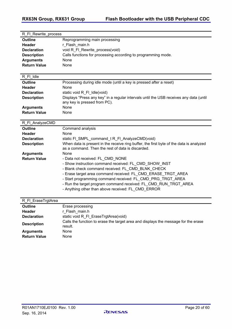
R_Fl_Rewrite_process Outline Reprogramming main processing Header r_Flash_main.h Declaration void R_Fl_Rewrite_process(void) Description Calls functions for processing according to programming mode. Arguments None Return Value None R_Fl_Idle Outline Processing during idle mode (until a key is pressed after a reset) Header None Declaration static void R_Fl_Idle(void) Description Displays “Press any key” in a regular intervals until the USB receives any data (until
any key is pressed from PC). Arguments None Return Value None R_Fl_AnalyzeCMD Outline Command analysis Header None Declaration static Fl_SMPL_command_t R_Fl_AnalyzeCMD(void) Description When data is present in the receive ring buffer, the first byte of the data is analyzed
as a command. Then the rest of data is discarded. Arguments None Return Value - Data not received: FL_CMD_NONE
- Show instruction command received: FL_CMD_SHOW_INST - Blank check command received: FL_CMD_BLNK_CHECK - Erase target area command received: FL_CMD_ERASE_TRGT_AREA - Start programming command received: FL_CMD_PRG_TRGT_AREA - Run the target program command received: FL_CMD_RUN_TRGT_AREA - Anything other than above received: FL_CMD_ERROR
R_Fl_EraseTrgtArea Outline Erase processing Header r_Flash_main.h Declaration static void R_Fl_EraseTrgtArea(void)
Description Calls the function to erase the target area and displays the message for the erase result.
Arguments None Return Value None
RX63N Group, RX631 Group Flash Bootloader with the USB Peripheral CDC
R01AN1710EJ0100 Rev. 1.00 Page 21 of 60 Sep. 16, 2014
R_Fl_PrgTrgtArea Outline Program processing Header None Declaration static void R_Fl_PrgTrgtArea(void) Description When data is present in the receive ring buffer, calls the function to store the data in
Motorola S format. When one record of Motorola S format data is received, calls the function to analyze the header and convert the data to binary data. When the conversion to binary data is completed, calls the function to store the converted data in the programming buffer.
Arguments None Return Value None R_Fl_RunTrgtPrg Outline Executing the target program Header None Declaration static void R_Fl_RunTrgtPrg(void) Description If the target reset vector is a value other than FFFF FFFFh, stops the USB and then
executes the target program. If the target reset vector is FFFF FFFFh, displays the message for target vector error.
Arguments None Return Value None R_Fl_ErrorWait Outline Error end wait mode processing Header None Declaration static void R_Fl_ErrorWait(void) Description If a certain period of time elapsed while the receive ring buffer is empty, the MCU
enters command wait mode. If there is any data in the receive ring buffer, the data is discarded and then a wait processing for a certain period is performed again.
Arguments None Return Value None R_Fl_cmd_ShowInst Outline Displaying commands Header None Declaration static void R_Fl_cmd_ShowInst(void) Description Displays commands. Arguments None Return Value None R_Fl_cmd_BlankCheckStart Outline Start processing for blank check Header None Declaration static void R_Fl_cmd_BlankCheckStart(void) Description Calls the function to blank check for the target area and displays the message for the
result. Arguments None Return Value None

RX63N Group, RX631 Group Flash Bootloader with the USB Peripheral CDC
R01AN1710EJ0100 Rev. 1.00 Page 22 of 60 Sep. 16, 2014
R_Fl_cmd_EraseStart Outline Start processing for erasing Header None Declaration static void R_Fl_cmd_ EraseStart (void)
Description Starts erasing the target area and displays the message for starting an erase operation.
Arguments None Return Value None R_Fl_cmd_PrgStart Outline Start processing for programming Header None Declaration static void R_Fl_cmd_PrgStart(void)
Description Starts programming the target area and displays the message for starting a program operation.
Arguments None Return Value None R_Fl_cmd_RunTrgtPrgStart Outline Executing the target program Header None Declaration static void R_Fl_cmd_RunTrgtPrgStart(void) Description If the target vector is FFFF FFFFh, the message for the target vector error is
transmitted. If the target vector is not FFFF FFFFh, the message for target program execution is displayed and the MCU enters program execution mode.
Arguments None Return Value None R_Fl_Blnk_BlankCheck Outline Blank check Header None Declaration Fl_API_SMPL_rtn_t R_Fl_Blnk_BlankCheck(void) Description Performs a blank check for the target area. Arguments None Return Value - When the target area is blank: FLASH_API_SAMPLE_OK
- When the target area is not blank: FLASH_API_SAMPLE_NG R_Fl_Ers_EraseFlash Outline Erasing the target area Header None Declaration Fl_API_SMPL_rtn_t R_Fl_Ers_EraseFlash(void) Description Erases the target area. Arguments None Return Value - When the erase is completed successfully: FLASH_API_SAMPLE_OK
- When the erase is failed: FLASH_API_SAMPLE_NG Remarks To avoid a ROM access by an interrupt during the erase operation, the processor
interrupt priority level (IPL) for the processor status word (PSW) is changed.

RX63N Group, RX631 Group Flash Bootloader with the USB Peripheral CDC
R01AN1710EJ0100 Rev. 1.00 Page 23 of 60 Sep. 16, 2014
R_Fl_Prg_StoreMotS Outline Storing Motorola S format data Header None Declaration static Fl_API_SMPL_rtn_t R_Fl_Prg_StoreMotS(uint8_t) Description Stores the data, which is received with the argument, in Motorola S format in bytes.
Any data is discarded until 'S' in ASCII is received. Arguments mot_data: Motorola S format data Return Value - When one record of Motorola S format data (from 'S' to checksum) is stored:
FLASH_API_SAMPLE_OK - When the stored Motorola S format data is not enough for one record: FLASH_API_SAMPLE_NG
Remarks - To use this function, one byte of Motorola S format data is passed repeatedly with the argument. - Checksum is not calculated.
R_Fl_Prg_ProcessForMotS_data Outline Motorola S format header analysis and binary data conversion Header None Declaration static void R_Fl_Prg_ProcessForMotS_data(void) Description Analyzes the Motorola S format header and calls the function to convert the data to
binary. If there is non-Motorola S format data, the error message is displayed. Arguments None Return Value None R_Fl_Prg_MotS_AsciiToBinary Outline ASCII to binary conversion of Motorola S format data Header None Declaration static Fl_API_SMPL_rtn_t R_Fl_Prg_MotS_AsciiToBinary (Fl_prg_mot_s_t *,
Fl_prg_mot_s_binary_t *) Description Converts Motorola S format in ASCII to binary data and verifies the checksum of the
converted binary data. If there is non-Motorola S format data, the error message is displayed. If a checksum error occurs, the error message is displayed.
Arguments First argument: *tmp_mot_s: Pointer to Motorola S format data in ASCII Second argument: *tmp_mot_s_binary: Pointer to the variable for storing data
which is converted to binary Return Value - When conversion is completed: FLASH_API_SAMPLE_OK
- When conversion is not completed: FLASH_API_SAMPLE_NG R_Fl_Prg_MakeWriteData Outline Making programming data Header None Declaration static Fl_API_SMPL_rtn_t R_Fl_Prg_MakeWriteData(void) Description Makes data separated by 256 bytes. Arguments None Return Value - When 256 bytes of programming data is made successfully:
FLASH_API_SAMPLE_OK - When 256 bytes of programming data is not made: FLASH_API_SAMPLE_NG

RX63N Group, RX631 Group Flash Bootloader with the USB Peripheral CDC
R01AN1710EJ0100 Rev. 1.00 Page 24 of 60 Sep. 16, 2014
R_Fl_Prg_WriteData Outline Programming the target area Header None Declaration static Fl_API_SMPL_rtn_t R_Fl_Prg_WriteData(void) Description Programming is performed for the target area and verifies the programmed data. If
the programming is failed, the error message is displayed. If the verify error occurs, the error message is displayed.
Arguments None Return Value - When programming is completed successfully: FLASH_API_SAMPLE_OK
- When programming is failed: FLASH_API_SAMPLE_NG Remarks To avoid a ROM access by an interrupt during the programming operation, the
processor interrupt priority level (IPL) for the processor status word (PSW) is changed.
R_Fl_Prg_ClearMotSVariables Outline Clearing variables for Motorola S format data Header None Declaration static void R_Fl_Prg_ClearMotSVariables(void) Description Clears variables for Motorola S format data. Arguments None Return Value None R_Fl_Run_StopUSB Outline Stopping USB Header iodefine.h, r_usb_usrconfig.h Declaration static void R_Fl_Run_StopUSB(void) Description Stops the USB. Arguments None Return Value None R_Fl_RcvDataString Outline Storing USB receive data Header R_Flash_main.h Declaration Fl_API_SMPL_rtn_t R_Fl_RcvDataString(void *, uint16_t) Description Stores data received by the USB in the receive ring buffer. Arguments First argument: *tranadr: Pointer to the buffer for storing data received by the
USB Second argument: length: The number of data received by the USB
Return Value - When the received data is stored successfully: FLASH_API_SAMPLE_OK - When the receive ring buffer was full: FLASH_API_SAMPLE_NG
R_Fl_SetSendData Outline Storing USB transmit data Header R_Flash_main.h Declaration uint16_t R_Fl_SetSendData(void *, uint16_t) Description Stores data to be transmitted by the USB in the transmit ring buffer. Arguments First argument: *tranadr: Pointer to the transmit buffer
Second argument: length_lim: Limit number of data stored in the transmit buffer Return Value The number of data stored in the transmit buffer

RX63N Group, RX631 Group Flash Bootloader with the USB Peripheral CDC
R01AN1710EJ0100 Rev. 1.00 Page 25 of 60 Sep. 16, 2014
R_Fl_SetDisplayMsgData Outline Setting message data to be displayed (dot display) Header None Declaration static Fl_API_SMPL_rtn_t R_Fl_SetDisplayMsgData(Fl_disp_tbl_num_t) Description Stores the specified message in the transmit ring buffer. Arguments table_num: Message number to be displayed Return Value - When the transmit data is stored successfully: FLASH_API_SAMPLE_OK
- When the transmit ring buffer was full: FLASH_API_SAMPLE_NG R_Fl_RingCheckBlank Outline Checking receive ring buffer space Header R_Flash_main.h Declaration Fl_API_SMPL_rtn_t R_Fl_RingCheckBlank(void) Description Checks whether the receive ring buffer has enough space for a USB reception (64
bytes). Arguments None Return Value - When the buffer has enough space: FLASH_API_SAMPLE_OK
- When the buffer does not have enough space: FLASH_API_SAMPLE_NG R_Fl_Ring2CheckData Outline Checking data in the transmit ring buffer Header R_Flash_main.h Declaration Fl_API_SMPL_rtn_t R_Fl_Ring2CheckData(void) Description Checks whether data is present in the transmit ring buffer. Arguments None Return Value - When data is present: FLASH_API_SAMPLE_OK
- When no data is present: FLASH_API_SAMPLE_NG R_Fl_USB_NonConnect_Run Outline Executing the target program with the USB disconnected Header R_Flash_main.h Declaration void R_Fl_USB_NonConnect_Run(void) Description Stops the USB and executes the target program. Arguments None Return Value None Remarks This function is called when the USB is disconnected. R_Fl_RingEnQueue Outline Storing data in the receive ring buffer Header r_Flash_buff.h Declaration Fl_API_SMPL_rtn_t R_Fl_RingEnQueue(uint8_t) Description Stores data in the receive ring buffer. Arguments enq_data: Data to be stored Return Value - When data is stored successfully: FLASH_API_SAMPLE_OK
- When the buffer was full: FLASH_API_SAMPLE_NG

RX63N Group, RX631 Group Flash Bootloader with the USB Peripheral CDC
R01AN1710EJ0100 Rev. 1.00 Page 26 of 60 Sep. 16, 2014
R_Fl_RingDeQueue Outline Reading the receive ring buffer Header r_Flash_buff.h Declaration Fl_API_SMPL_rtn_t R_Fl_RingDeQueue(uint8_t *) Description Reads data from the receive ring buffer. Arguments *deq_data: Pointer to the buffer for storing the read data Return Value - When data is read successfully: FLASH_API_SAMPLE_OK
- When no data to be read is present: FLASH_API_SAMPLE_NG R_Fl_RingClear Outline Clearing the receive ring buffer Header r_Flash_buff.h Declaration Fl_API_SMPL_rtn_t R_Fl_RingClear(void) Description Clears the receive ring buffer. Arguments None Return Value FLASH_API_SAMPLE_OK is always returned. R_Fl_RingCheck Outline Checking the number of data in the receive ring buffer Header r_Flash_buff.h Declaration uint32_t R_Fl_RingCheck(void) Description Checks the number of data in the receive ring buffer. Arguments None Return Value The number of received data is returned. R_Fl_Ring2EnQueue Outline Storing data in the transmit ring buffer Header r_Flash_buff.h Declaration Fl_API_SMPL_rtn_t R_Fl_Ring2EnQueue(uint8_t) Description Stores data in the transmit ring buffer. Arguments enq_data: data to be stored Return Value - When data is stored successfully: FLASH_API_SAMPLE_OK
- When the buffer was full: FLASH_API_SAMPLE_NG R_Fl_Ring2DeQueue Outline Reading the transmit ring buffer Header r_Flash_buff.h Declaration Fl_API_SMPL_rtn_t R_Fl_Ring2DeQueue(uint8_t *) Description Reads data in the transmit ring buffer. Arguments *deq_data: Pointer to the buffer for storing the read data Return Value - When data is read successfully: FLASH_API_SAMPLE_OK
- When no data to be read is present: FLASH_API_SAMPLE_NG

RX63N Group, RX631 Group Flash Bootloader with the USB Peripheral CDC
R01AN1710EJ0100 Rev. 1.00 Page 27 of 60 Sep. 16, 2014
R_Fl_Ring2Clear Outline Clearing the transmit ring buffer Header r_Flash_buff.h Declaration Fl_API_SMPL_rtn_t R_Fl_Ring2Clear(void) Description Clears the transmit ring buffer. Arguments None Return Value FLASH_API_SAMPLE_OK is always returned. R_Fl_Ring2Check Outline Checking the number of data in the transmit ring buffer Header r_Flash_buff.h Declaration uint32_t R_Fl_Ring2Check(void) Description Checking the number of data in the transmit ring buffer. Arguments None Return Value The number of transmit data is returned. R_Fl_AsciiToHexByte Outline ASCII to Binary conversion Header r_Flash_buff.h Declaration uint8_t R_Fl_AsciiToHexByte(uint8_t, uint8_t) Description Converts 2-byte ASCII data to 1-byte binary data. Arguments First argument: in_upper: Upper byte of ASCII data Second argument: in_lower: Lower byte of ASCII data Return Value Converted binary data is returned.

RX63N Group, RX631 Group Flash Bootloader with the USB Peripheral CDC
R01AN1710EJ0100 Rev. 1.00 Page 28 of 60 Sep. 16, 2014
5.13 Flowcharts 5.13.1 USB Main Processing Figure 5.9 and Figure 5.10 show the USB Main Processing.
usb_pcdc_main_task
Receiving messageR_USB_TRCV_MSG()
Is the message for periodic
activation?
Periodic activation: USB_PCDC_PERIODIC_PROCESS
Transmitting messageusb_pcdc_smpl_message_send()
Periodic activation request to this task
Is the state of the USB transmitting
flag ON?
Reprogramming main processing
R_Fl_Rewrite_process()
Is data to be transmitted by the USB
present?
Storing USB transmit dataR_FI_SetSendData()
Transmitting datawrite()
Set the USB transmitting flag to on
Is the state of the USB next reception
request flag ON?
Is there enough space in the
receive buffer for next USB data?
Receiving dataread()
Set the USB next reception request flag to off
usb_gpcdc_tx_wait_flag = USB_OFF
usb_gpcdc_tx_wait_flag = USB_ON
Yes
No
USB reception completed: USB_PCDC_RX_COMP
Obtaining the number of data received by the USB
control()
Storing USB receive dataR_FI_RcvDataString()
Is there enough space in the
receive buffer for next USB data?
Receiving dataread()
USB transmission completed: USB_PCDC_TX_COMP
Is data to be transmitted
present?
Set the USB transmitting flag to off
Storing USB transmit dataR_Fl_SetSendData()
Transmitting datawrite()
Set the USB transmitting flag to on
Yes
No
Yes
No
Yes
No
Another message
Is data to be received by the USB
present?
Yes
No
ON
OFF
A
B
Set the USB next reception request flag to on
Figure 5.9 USB Main Processing (1/2)

RX63N Group, RX631 Group Flash Bootloader with the USB Peripheral CDC
R01AN1710EJ0100 Rev. 1.00 Page 29 of 60 Sep. 16, 2014
Is the message for close
request?
CLOSE request: USB_PCDC_CLOSE
The other message
CDCD openopen(USB_CLASS_PCDCD,,)
Is CDCD file number valid?
Has the USB been disconnected for a
certain time?
Executing the target program with the USB disconnected
R_Fl_USB_NonConnect_Run()
Transmitting the message for open request
usb_pcdc_smpl_message_send()
CDCC openopen(USB_CLASS_PCDCC,,)
Is CDCC file number valid?
Transmitting the message for periodic activation
usb_pcdc_smpl_message_send()
Is CDCD file number valid?
CDCD closeclose(CDCD file No,,)
Is CDCD file number valid?
CDCD closeclose(CDCC file No,,)
Initializing application variablesusb_pcdc_apl_init()
Valid (0x10 to 0x1f)
Invalid (-1)
Invalid (-1)
Valid (0x10 to 0x1f)
Valid (0x10 to 0x1f)
Invalid (-1)
OPEN request: USB_PCDC_OPEN
Valid (0x10 to 0x1f)
Invalid (-1)
No
Yes
A
B
Figure 5.10 USB Main Processing (2/2)

RX63N Group, RX631 Group Flash Bootloader with the USB Peripheral CDC
R01AN1710EJ0100 Rev. 1.00 Page 30 of 60 Sep. 16, 2014
5.13.2 Reprogramming Main Processing Figure 5.11 shows the Reprogramming Main Processing.
R_Fl_Rewrite_process
Mode determination
IDLE
Processing during idle modeR_Fl_Idle()
Command analysisR_Fl_AnalyzeCMD()
Command determination
Erase processingR_Fl_EraseTrgtArea()
Program processingR_Fl_PrgTrgtArea()
Executing the target program R_Fl_RunTrgtPrg()
Wait for completion of an error processingR_Fl_ErrorWait()
Displaying commandsR_Fl_cmd_ShowInst()
Command wait
Start processing for blank check
R_Fl_cmd_BlankCheckStart()
Start processing for erasingR_Fl_cmd_EraseStart()
Start processing for programming
R_Fl_cmd_PrgStart()
Executing the target programR_Fl_cmd_RunTrgtPrgStart()
Displaying commandsR_Fl_cmd_ShowInst()
return
Erase
Program
Program execution
Error end wait
Show instructions
Blank check
Erase target area
Start programming
Run the target program
default
None
default
Enters Error end wait mode
Figure 5.11 Reprogramming Main Processing

RX63N Group, RX631 Group Flash Bootloader with the USB Peripheral CDC
R01AN1710EJ0100 Rev. 1.00 Page 31 of 60 Sep. 16, 2014
5.13.3 Processing During Idle Mode Figure 5.12 shows the Processing During Idle Mode.
R_Fl_Idle
Is received data present?
Yes
return
Displaying commandsR_Fl_cmd_ShowInst()
No
Did a certain amount of time
elapse?
Display the message for idleR_Fl_SetDisplayMsgData()
Clear the counter
Elapsed
Not elapsed
Enter command wait mode
Checking the number of data in the receive ring buffer
R_Fl_RingCheck()
Clearing the receive bufferR_Fl_RingClear()
Counter + 1
Figure 5.12 Processing During Idle Mode

RX63N Group, RX631 Group Flash Bootloader with the USB Peripheral CDC
R01AN1710EJ0100 Rev. 1.00 Page 32 of 60 Sep. 16, 2014
5.13.4 Command Analysis Figure 5.13 shows the Command Analysis.
R_Fl_AnalyzeCMD
Is receive data present?
Yes
return ret_code
No
Command determination
Set 'Instruction' as the return value
Set 'Blank' as the return value
Set 'Erase' as the return value
Set 'Program' as the return value
Set 'Run' as the return value
Set 'Error' as the return value
0x31
0x32
0x33
0x34
0x35
default
Set the return value to 'None'
Clearing the receive ring buffer
R_Fl_RingClear()
Reading the receive ring buffer
R_Fl_RingDeQueue()
Figure 5.13 Command Analysis

RX63N Group, RX631 Group Flash Bootloader with the USB Peripheral CDC
R01AN1710EJ0100 Rev. 1.00 Page 33 of 60 Sep. 16, 2014
5.13.5 Erase Processing Figure 5.14 shows the Erase Processing.
R_Fl_EraseTrgtArea
Was the erase operation completed
successfully?
Yes
return
No
Erasing the target areaR_Fl_Ers_EraseFlash
Enter command wait mode
Display the message for erase succeeded
R_Fl_SetDisplayMsgData()
Display the message for erase failed
R_Fl_SetDisplayMsgData()
Figure 5.14 Erase Processing
5.13.6 Program Processing Figure 5.15 shows the Program Processing.
R_Fl_PrgTrgtArea
Is the MotS binary data present?
Yes
return
NoMaking programming data
R_Fl_Prg_MakeWriteData()
Is receive data present?
Reading the receive ring bufferR_Fl_RingDeQueue()
No
Yes
Has one format data (address and data
only) been received?
Reception completed
Motorola S format header analysis and binary data conversion
R_Fl_Prg_ProcessForMotS_data()
Is the data to be programmed
ready?
No
Yes
Programming the target area
R_Fl_Prg_WriteData()Storing Motorola S format data
R_Fl_Prg_StoreMotS()
Reception not completed
Figure 5.15 Program Processing

RX63N Group, RX631 Group Flash Bootloader with the USB Peripheral CDC
R01AN1710EJ0100 Rev. 1.00 Page 34 of 60 Sep. 16, 2014
5.13.7 Executing the Target Program Figure 5.16 shows the Executing the Target Program.
R_Fl_RunTrgtPrg
return
Display the message for vector error
R_Fl_SetDisplayMsgData()
Is the target reset vector value
0xFFFF FFFF?No
Yes
Stopping USBR_Fl_Run_StopUSB()
Executing the target program
Enter command wait mode
Figure 5.16 Executing the Target Program

RX63N Group, RX631 Group Flash Bootloader with the USB Peripheral CDC
R01AN1710EJ0100 Rev. 1.00 Page 35 of 60 Sep. 16, 2014
5.13.8 Wait for Completion of an Error Processing Figure 5.17 shows the Wait for Completion of an Error Processing.
R_Fl_ErrorWait
Has a wait for error processing
started?Not started
return
Started
Is data received by the USB
present?No
Yes
Set the error wait start flag
Clear the error wait counter and the dot display counter
Display the message for a wait for error processing
R_Fl_SetDisplayMsgData()
Clear the error wait counter
Has the wait time for error processing
elapsed?
Display the message for new line
R_Fl_SetDisplayMsgData()
Yes
Clear the error wait start flag
Error wait counter + 1dot display counter + 1
Has the dot display time
elapsed?
dot displayR_Fl_SetDisplayMsgData()
Clear the dot display counter
No
Clearing the receive ring buffer
R_Fl_RingClear()
Yes
No
Display commandsR_Fl_SetDisplayMsgData()
Enter command wait mode
Clearing the receive ring buffer
R_Fl_RingClear()
Figure 5.17 Wait for Completion of an Error Processing

RX63N Group, RX631 Group Flash Bootloader with the USB Peripheral CDC
R01AN1710EJ0100 Rev. 1.00 Page 36 of 60 Sep. 16, 2014
5.13.9 Displaying Commands Figure 5.18 shows the Displaying Commands.
R_Fl_cmd_ShowInst
return
Displaying commandsR_Fl_SetDisplayMsgData()
Figure 5.18 Displaying Commands
5.13.10 Start Processing for Blank Check Figure 5.19 shows the Start Processing for Blank Check.
R_Fl_cmd_BlankCheckStart
return
Was the area blank?Not blank
Blank
Blank checkR_Fl_Blnk_BlankCheck()
Display the message for blank
R_Fl_SetDisplayMsgData()
Display the message for not blank
R_Fl_SetDisplayMsgData()
Figure 5.19 Start Processing for Blank Check
5.13.11 Start Processing for Erasing Figure 5.20 shows the Start Processing for Erasing.
R_Fl_cmd_EraseStart
return
Display the message for starting an erase operationR_Fl_SetDisplayMsgData()
Enter erase mode
Figure 5.20 Start Processing for Erasing
RX63N Group, RX631 Group Flash Bootloader with the USB Peripheral CDC
R01AN1710EJ0100 Rev. 1.00 Page 37 of 60 Sep. 16, 2014
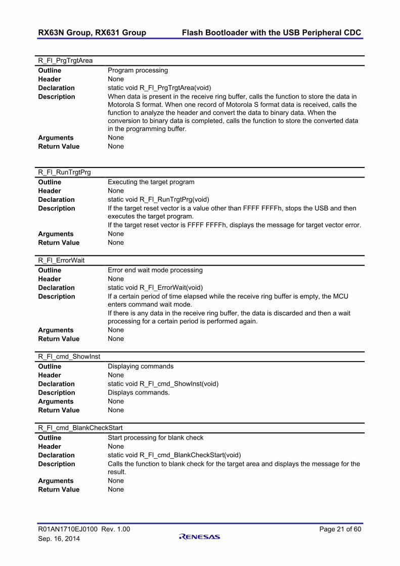
5.13.12 Start Processing for Programming Figure 5.21 shows the Start Processing for Programming.
R_Fl_cmd_PrgStart
return
Clearing variables for Motorola S format data
R_Fl_Prg_ClearMotSVariables()
Display the message for starting a program operation
R_Fl_SetDisplayMsgData()
Enter program mode
Figure 5.21 Start Processing for Programming
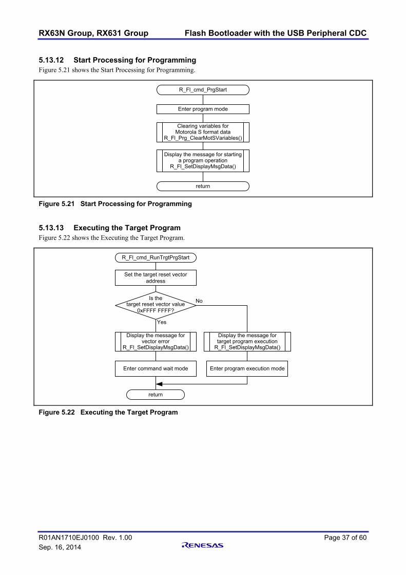
5.13.13 Executing the Target Program Figure 5.22 shows the Executing the Target Program.
R_Fl_cmd_RunTrgtPrgStart
return
Set the target reset vector address
Is the target reset vector value
0xFFFF FFFF?
No
Display the message for vector error
R_Fl_SetDisplayMsgData()
Yes
Enter command wait mode
Display the message for target program execution
R_Fl_SetDisplayMsgData()
Enter program execution mode
Figure 5.22 Executing the Target Program

RX63N Group, RX631 Group Flash Bootloader with the USB Peripheral CDC
R01AN1710EJ0100 Rev. 1.00 Page 38 of 60 Sep. 16, 2014
5.13.14 Blank Check Figure 5.23 shows the Blank Check.
R_Fl_Blnk_BlankCheck
return ret_code
Set 'OK' to ret_code
Have all addresses been
checked?
Yes
No
Set 'NG' to ret_code
Address for checking + 1
Address for checking - 1
Was the checked address
blank?
Yes
No
Set the end address
Figure 5.23 Blank Check

RX63N Group, RX631 Group Flash Bootloader with the USB Peripheral CDC
R01AN1710EJ0100 Rev. 1.00 Page 39 of 60 Sep. 16, 2014
5.13.15 Erasing the Target Area Figure 5.24 shows the Erasing the Target Area.
R_Fl_Ers_EraseFlash
return ret_code
Set 'OK' to ret_code
Has the target area been
erased?
Yes
No
Set 'NG' to ret_code
Has the area been erased
successfully?
Erasing flash(Simple Flash API function)
R_FlashErase()
Yes
No
Store current PSW.IPL
Set PSW.IPL toFLASH_READY_IPL(5)
Restore the original value into PSW.IPL
Figure 5.24 Erasing the Target Area

RX63N Group, RX631 Group Flash Bootloader with the USB Peripheral CDC
R01AN1710EJ0100 Rev. 1.00 Page 40 of 60 Sep. 16, 2014
5.13.16 Storing Motorola S Format Data Figure 5.25 shows the Storing Motorola S Format Data.
R_Fl_Prg_StoreMotS
return ret_code
Set 'NG' to ret_code
Check for the number of MotS
data
0
Clear the counter and set 'OK' to ret_code
ASCII to Binary conversionof data length
R_Fl_AsciiToHexByte()
MotS data = 'S'?
Store the upper byte of the header and increment the counter
'S'
Other than 'S'
1
2
3
Store the MotS data and increment the counter
default
Has one format data (address and data only) been
received?
Reception completed
Reception not completed
Store the lower byte of the header and increment the counter
Store the upper byte of the data length and increment the counter
Store the lower byte of the data length and increment the counter
Figure 5.25 Storing Motorola S Format Data

RX63N Group, RX631 Group Flash Bootloader with the USB Peripheral CDC
R01AN1710EJ0100 Rev. 1.00 Page 41 of 60 Sep. 16, 2014
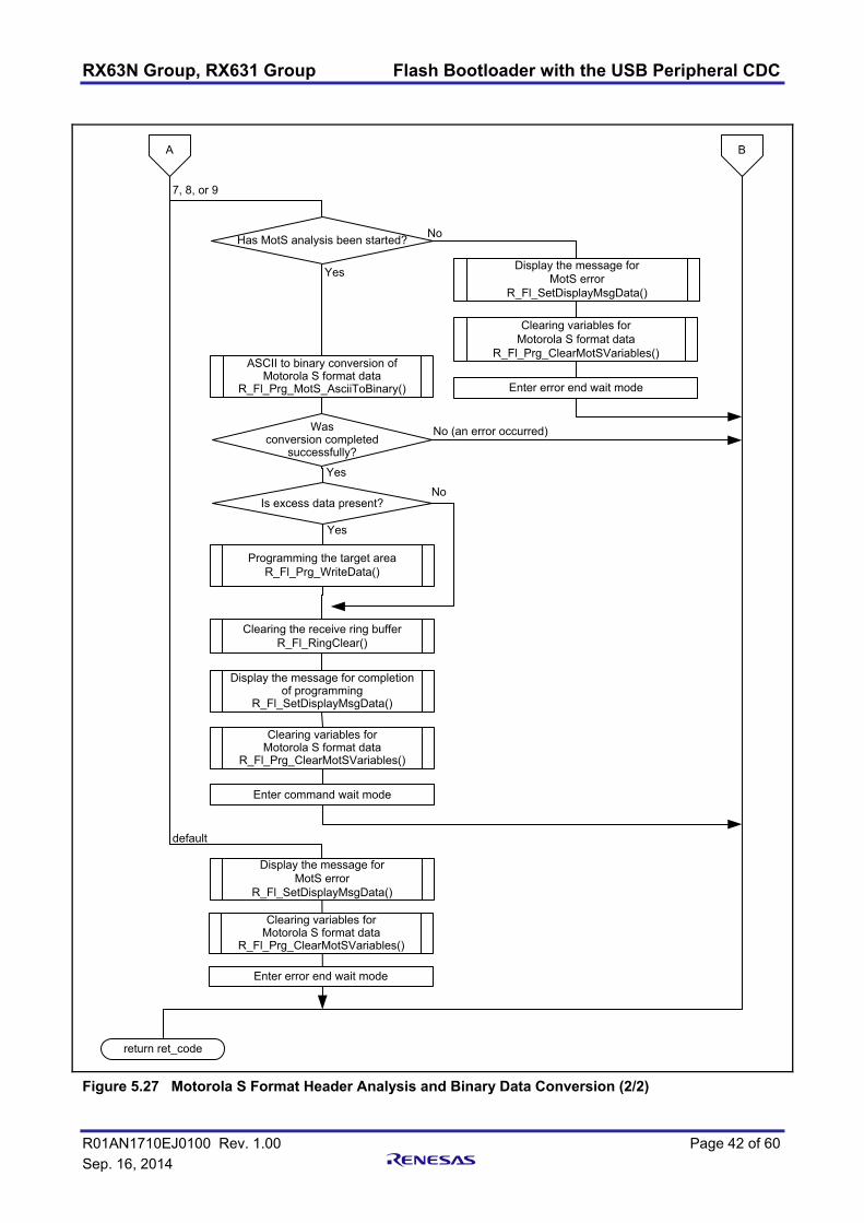
5.13.17 Motorola S Format Header Analysis and Binary Data Conversion Figure 5.26 and Figure 5.27 show the Motorola S Format Header Analysis and Binary Data Conversion.
R_Fl_Prg_ProcessForMotS_data
Check the value in the lower byte of the
header
0
Set the MotS analysis start flag
3
ASCII to Binary conversion of MotS
R_Fl_Prg_MotS_AsciiToBinary()
Was conversion completed
successfully?
Yes
No (an error occurred)
Set the MotS data completion flag
Has MotS analysis been
started?
Yes
No
ASCII to Binary conversion of MotS
R_Fl_Prg_MotS_AsciiToBinary()
Display the message for MotS error
R_Fl_SetDisplayMsgData()
Clearing variables for Motorola S format data
R_Fl_Prg_ClearMotSVariables()
Enter error end wait mode
Has MotS analysis been
started?Display the message for
MotS errorR_Fl_SetDisplayMsgData()
Clearing variables for Motorola S format data
R_Fl_Prg_ClearMotSVariables()
Enter error end wait mode
Yes
No
A B
Figure 5.26 Motorola S Format Header Analysis and Binary Data Conversion (1/2)
RX63N Group, RX631 Group Flash Bootloader with the USB Peripheral CDC
R01AN1710EJ0100 Rev. 1.00 Page 42 of 60 Sep. 16, 2014
return ret_code
7, 8, or 9
default
ASCII to binary conversion of Motorola S format data
R_Fl_Prg_MotS_AsciiToBinary()
Was conversion completed
successfully?
Yes
No (an error occurred)
Is excess data present?
Programming the target areaR_Fl_Prg_WriteData()
Yes
No
Clearing the receive ring bufferR_Fl_RingClear()
Display the message for completion of programming
R_Fl_SetDisplayMsgData()
Clearing variables for Motorola S format data
R_Fl_Prg_ClearMotSVariables()
Enter command wait mode
Display the message for MotS error
R_Fl_SetDisplayMsgData()
Clearing variables for Motorola S format data
R_Fl_Prg_ClearMotSVariables()
Enter error end wait mode
No
Yes Display the message for MotS error
R_Fl_SetDisplayMsgData()
Clearing variables for Motorola S format data
R_Fl_Prg_ClearMotSVariables()
Enter error end wait mode
A B
Has MotS analysis been started?
Figure 5.27 Motorola S Format Header Analysis and Binary Data Conversion (2/2)

RX63N Group, RX631 Group Flash Bootloader with the USB Peripheral CDC
R01AN1710EJ0100 Rev. 1.00 Page 43 of 60 Sep. 16, 2014
5.13.18 ASCII to Binary Conversion of Motorola S Format Data Figure 5.28 shows the ASCII to Binary Conversion of Motorola S Format Data.
R_Fl_Prg_MotS_AsciiToBinary
return ret_code
ASCII to Binary conversion of data length
R_Fl_AsciiToHexByte()
Store the data length (subtract length of checksum and
address)
Display the message for checksum error
R_Fl_SetDisplayMsgData()
Yes
No
Set 'NG' to ret_code
Clearing variables for Motorola S format data
R_Fl_Prg_ClearMotSVariables()
Enter error end wait mode
Did achecksum error
occur?
Store the address
Store the data
Set 'OK' to ret_code
Convert all data to binary data
Figure 5.28 ASCII to Binary Conversion of Motorola S Format Data

RX63N Group, RX631 Group Flash Bootloader with the USB Peripheral CDC
R01AN1710EJ0100 Rev. 1.00 Page 44 of 60 Sep. 16, 2014
5.13.19 Making Programming Data Figure 5.29 shows the Making Programming Data.
R_Fl_Prg_MakeWriteData
return ret_code
Set 'NG' to ret_code
Total of programming data ≥
256?
> 256
≤ 256
Has the programming address
been specified?
Yes
No
Store MotS data (binary) in the programming buffer
Specify the programming address
Total of the programming data
> 256?
≥ 256
≤ 257
Store 256 bytes of MotS data (binary) in the programming buffer
Store excess data and set the programming address for the
excess data
Clear the MotS data completion flag
Set 'OK' to ret_code
Figure 5.29 Making Programming Data

RX63N Group, RX631 Group Flash Bootloader with the USB Peripheral CDC
R01AN1710EJ0100 Rev. 1.00 Page 45 of 60 Sep. 16, 2014
5.13.20 Programming the Target Area Figure 5.30 show the Programming the Target Area.
R_Fl_Prg_WriteData
return ret_code
Has the area been programmed
successfully?
Yes
No
Set 'OK' to ret_code
Programming Flash(Simple Flash API function)
R_FlashWrite()
Display the message for programming error
R_Fl_SetDisplayMsgData()
Clearing variables for Motorola S format data
R_Fl_Prg_ClearMotSVariables()
Enter error end wait mode
Set 'NG' to ret_code
Read the programmed data
Is the programmed data correct?
Yes
No
Display the message for verify errorR_Fl_SetDisplayMsgData()
Clearing variables for Motorola S format data
R_Fl_Prg_ClearMotSVariables()
Enter error end wait mode
Set 'NG' to ret_code
Clear the programming addressand the programming buffer
Has the programming address for
excess data been specified?
Yes
No
Store the excess data in the programming buffer
Clear the MotS data completion flag
Clear the programming address for excess data
Set the programming address
Restore the original value into PSW.IPL
Store the current PSW.IPL
Set PSW.IPL toFLASH_READY_IPL(5)
Figure 5.30 Programming the Target Area

RX63N Group, RX631 Group Flash Bootloader with the USB Peripheral CDC
R01AN1710EJ0100 Rev. 1.00 Page 46 of 60 Sep. 16, 2014
5.13.21 Clearing Variables for Motorola S Format Data Figure 5.31 shows the Clearing Variables for Motorola S Format Data.
R_Fl_Prg_ClearMotSVariables
return ret_code
- Clear the MotS data completion flag- Clear the MotS analysis start flag- Clear the programming address for excess data- Clear the programming address- Clear the programming buffer
Figure 5.31 Clearing Variables for Motorola S Format Data

RX63N Group, RX631 Group Flash Bootloader with the USB Peripheral CDC
R01AN1710EJ0100 Rev. 1.00 Page 47 of 60 Sep. 16, 2014
5.13.22 Stopping USB Figure 5.32 shows the Stopping USB.
R_Fl_Run_StopUSB
return ret_code
Disable USB0 module operation
Disable USB0 interrupt request
Clear USB0 interrupt request
Enter the USB0 module-stop state
USB0.SYSCFG register USBE bit ← 0: USB operation is disabled.
IER04 register IEN1 bit ← 0: Interrupt request is disabled. IEN2 bit ← 0: Interrupt request is disabled. IEN3 bit ← 0: Interrupt request is disabled.IER0B register IEN2 bit ← 0: Interrupt request is disabled.
IR33 register IR bit ← 0: No interrupt request is generated.IR34 register IR bit ← 0: No interrupt request is generated.IR35 register IR bit ← 0: No interrupt request is generated.
MSTPCRB register MSTPB19 bit ← 1: Transition to the module-stop state is made.
Disable USB1 module operation
Disable USB1 interrupt request
Clear USB1 interrupt request
Enter the USB1 module-stop state
USB1.SYSCFG register USBE bit ← 0: USB operation is disabled.
IER04 register IEN4 bit ← 0: Interrupt request is disabled. IEN5 bit ← 0: Interrupt request is disabled. IEN6 bit ← 0: Interrupt request is disabled.IER0B register IEN3 bit ← 0: Interrupt request is disabled.IR36 register IR bit ← 0: No interrupt request is generated.IR37 register IR bit ← 0: No interrupt request is generated.IR38 register IR bit ← 0: No interrupt request is generated.
MSTPCRB register MSTPB18 bit ← 1: Transition to the module-stop state is made.
Executed when USB_FUNCSEL_USBIP1_PP == USB_PERI_PP
Enable writing to related registers PRCR register ← A502h PRC1 bit = 1
Disable writing to related registers PRCR register ← A500h PRC1 bit = 0
Executed when USB_FUNCSEL_USBIP0_PP == USB_PERI_PP
Figure 5.32 Stopping USB

RX63N Group, RX631 Group Flash Bootloader with the USB Peripheral CDC
R01AN1710EJ0100 Rev. 1.00 Page 48 of 60 Sep. 16, 2014
5.13.23 Storing USB Receive Data Figure 5.33 shows the Storing USB Receive Data.
R_Fl_RcvDataString
return ret_code
Set 'OK' to ret_code
Is there enough space in the receive
buffer?
No
Checking the number of data in the receive ring buffer
R_Fl_RingCheck()
Yes
Store receive data Set 'NG' to ret_code
Figure 5.33 Storing USB Receive Data
5.13.24 Storing USB Transmit Data Figure 5.34 shows the Storing USB Transmit Data.
R_Fl_SetSendData
return ret_code
Number of transmit data > space in the
transmit buffer?
Number of transmit data >space in the transmit buffer
Checking the number of data in the transmit ring buffer
R_Fl_Ring2Check()
Set the number of transmit data Set the number of transmit data for the space size in the transmit buffer
Number of transmit data ≤space in the transmit buffer
Set the number of data to ret_code
Set the transmit data for the number of transmit data
Figure 5.34 Storing USB Transmit Data
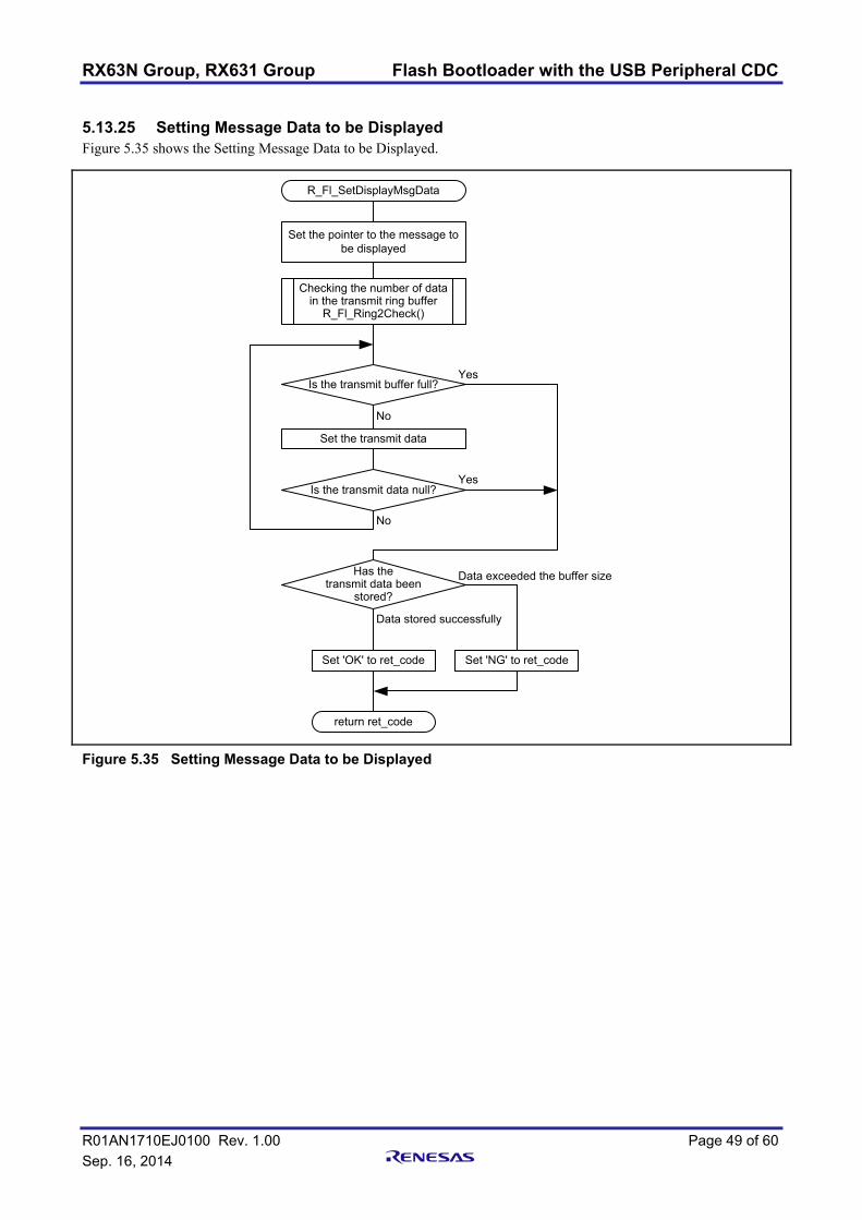
RX63N Group, RX631 Group Flash Bootloader with the USB Peripheral CDC
R01AN1710EJ0100 Rev. 1.00 Page 49 of 60 Sep. 16, 2014
5.13.25 Setting Message Data to be Displayed Figure 5.35 shows the Setting Message Data to be Displayed.
R_Fl_SetDisplayMsgData
return ret_code
Is the transmit buffer full?
No
Checking the number of data in the transmit ring buffer
R_Fl_Ring2Check()
Set the transmit data
Set 'OK' to ret_code
Set the pointer to the message to be displayed
Yes
Has the transmit data been
stored?
Data stored successfully
Data exceeded the buffer size
Set 'NG' to ret_code
Is the transmit data null?
No
Yes
Figure 5.35 Setting Message Data to be Displayed

RX63N Group, RX631 Group Flash Bootloader with the USB Peripheral CDC
R01AN1710EJ0100 Rev. 1.00 Page 50 of 60 Sep. 16, 2014
5.13.26 Checking Receive Ring Buffer Space Figure 5.36 shows the Checking Receive Ring Buffer Space.
R_Fl_RingCheckBlank
return ret_code
Checking the number of data in the receive ring buffer
R_Fl_RingCheck()
Set 'OK' to ret_code
Is there enough space for
the number of bytes the USB receives?
Yes
No
Set 'NG' to ret_code
Figure 5.36 Checking Receive Ring Buffer Space
5.13.27 Checking Data in the Transmit Ring Buffer Figure 5.37 shows the Checking Data in the Transmit Ring Buffer.
R_Fl_Ring2CheckData
return ret_code
Checking the number of data in the transmit ring buffer
R_Fl_Ring2Check()
Set 'OK' to ret_code
Is transmit data present?
Yes
No
Set 'NG' to ret_code
Figure 5.37 Checking Data in the Transmit Ring Buffer

RX63N Group, RX631 Group Flash Bootloader with the USB Peripheral CDC
R01AN1710EJ0100 Rev. 1.00 Page 51 of 60 Sep. 16, 2014
5.13.28 Executing the Target Program with the USB Disconnected Figure 5.38 shows the Executing the Target Program with the USB Disconnected.
R_Fl_USB_NonConnect_Run
Is the target reset vector value
0xFFFF FFFF?
No
Yes
Stopping USBR_Fl_Run_StopUSB()
Executing the target program
return
Figure 5.38 Executing the Target Program with the USB Disconnected
5.13.29 Storing Data in the Receive Ring Buffer Figure 5.39 shows the Storing Data in the Receive Ring Buffer.
R_Fl_RingEnQueue
Is there any space in the receive
buffer
Yes
No
return
Store data
Set 'OK' as the return value Set 'NG' as the return value
Figure 5.39 Storing Data in the Receive Ring Buffer

RX63N Group, RX631 Group Flash Bootloader with the USB Peripheral CDC
R01AN1710EJ0100 Rev. 1.00 Page 52 of 60 Sep. 16, 2014
5.13.30 Reading the Receive Ring Buffer Figure 5.40 shows the Reading the Receive Ring Buffer.
R_Fl_RingDeQueue
Is there data in the buffer?
Yes
No
return
Read the data
Set 'OK' as the return value Set 'NG' as the return value
Figure 5.40 Reading the Receive Ring Buffer
5.13.31 Clearing the Receive Ring Buffer Figure 5.41 shows the Clearing the Receive Ring Buffer.
R_Fl_RingClear
return
Clear the buffer pointer
Figure 5.41 Clearing the Receive Ring Buffer
5.13.32 Checking the Number of Data in the Receive Ring Buffer Figure 5.42 shows the Checking the Number of Data in the Receive Ring Buffer.
R_Fl_RingCheck
return
Set the number of dataas the return value
Figure 5.42 Checking the Number of Data in the Receive Ring Buffer

RX63N Group, RX631 Group Flash Bootloader with the USB Peripheral CDC
R01AN1710EJ0100 Rev. 1.00 Page 53 of 60 Sep. 16, 2014
5.13.33 Storing Data in the Transmit Ring Buffer Figure 5.43 shows the Storing Data in the Transmit Ring Buffer.
R_Fl_Ring2EnQueue
Is there enough space
for storing data in the buffer?
Yes
No
return
Store data
Set 'OK' as the return value Set 'NG' as the return value
Figure 5.43 Storing Data in the Transmit Ring Buffer
5.13.34 Reading the Transmit Ring Buffer Figure 5.44 shows the Reading the Transmit Ring Buffer.
R_Fl_Ring2DeQueue
Is there data in the buffer?
Yes
No
return
Read data
Set 'OK' as the return value Set 'NG' as the return value
Figure 5.44 Reading the Transmit Ring Buffer
5.13.35 Clearing the Transmit Ring Buffer Figure 5.45 shows the Clearing the Transmit Ring Buffer.
R_Fl_Ring2Clear
return
Clear the buffer pointer
Figure 5.45 Clearing the Transmit Ring Buffer

RX63N Group, RX631 Group Flash Bootloader with the USB Peripheral CDC
R01AN1710EJ0100 Rev. 1.00 Page 54 of 60 Sep. 16, 2014
5.13.36 Checking the Number of Data in the Transmit Ring Buffer Figure 5.46 shows the Checking the Number of Data in the Transmit Ring Buffer.
R_Fl_Ring2Check
return
Set the number of data as the return value
Figure 5.46 Checking the Number of Data in the Transmit Ring Buffer
5.13.37 ASCII to Binary Conversion Figure 5.47 shows the ASCII to Binary Conversion.
R_Fl_AsciiToHexByte
return
Convert upper 4 bits
Convert lower 4 bits
Figure 5.47 ASCII to Binary Conversion

RX63N Group, RX631 Group Flash Bootloader with the USB Peripheral CDC
R01AN1710EJ0100 Rev. 1.00 Page 55 of 60 Sep. 16, 2014
6. Using the Sample Code (1) Change the vendor ID and product ID for the sample code.
Change USB_VENDORID and USB_PRODUCTID in the r_usb_pcdc_descriptor.c file appropriate to your environment. Refer to the USB Peripheral Communication Device Class Driver and USB Basic Firmware application notes for details.
/******************************************************************************User define macro definitions******************************************************************************/#define USB_VENDORID 0x0000#define USB_PRODUCTID 0x0002
Figure 6.1 Vendor ID and Product ID in r_usb_pcdc_descriptor.c for the Sample Code
(2) Change the vendor ID and product ID for the USB driver. Change VID_0000 and PID_0002 in the CDC_Demo.inf or CDC_Demo_Win7.inf file in the usb_driver folder. The changed values must be the same as the vendor ID and product ID for the sample code set in step (1) above. Refer to the USB Peripheral Communication Device Class Driver and USB Basic Firmware application notes for details.
[Manufacturer] %STRING_MAUNUFACTURER%=Model
[Model] %STRING_MODEL%=CDC, USB\VID_0000&PID_0002
Figure 6.2 Vendor ID and Product ID in CDC_Demo.inf for the USB Driver
[DeviceList]%DESCRIPTION%=DriverInstall, USB\VID_0000&PID_0002
[DeviceList.NTamd64]%DESCRIPTION%=DriverInstall, USB\VID_0000&PID_0002
Figure 6.3 Vendor ID and Product ID in CDC_Demo_Win7.inf for the USB Driver
(3) Build all codes of the sample code and program the codes into the MCU.
(4) After the MCU is powered on, connect the PC and MCU via the USB. (1)
(5) In the Windows installation screen for the USB driver, select the CDC_Demo.inf or CDC_Demo_Win7.inf file in the usb_driver folder to install the driver. If the USB driver is already installed, this step can be skipped.
(6) Start the terminal application to start communication with the MCU.
(7) After step (6), follow the message displayed in the terminal application to continue the operation.
Note: 1. If a value other than FFFF FFFFh is written to the target reset vector, and the USB interface remains
disconnected for a certain time, the target program will be executed. Note that the USB will be stopped when the target program is executed. Write FFFF FFFFh to the target reset vector when the USB driver is installed since it may take some time to connect the USB interface.

RX63N Group, RX631 Group Flash Bootloader with the USB Peripheral CDC
R01AN1710EJ0100 Rev. 1.00 Page 56 of 60 Sep. 16, 2014
7. Sample Target Program A sample target program (UsrPrgSample.zip) is provided with this application note. In the sample target program, LEDs on the board listed on "2. Operation Confirmation Conditions" are turned on in order. Use this program as a reference when setting the target reset vector and sections. This program assumes an operation with 1 MB ROM.
8. Notes on Using This Application Note
8.1 Programming Speed Programming speed may be extremely slow depending on the terminal application used. If this is the case, try another terminal application.
8.2 USB Disconnection During Programming or Erasing Do not disconnect or reconnect the USB interface during programming or erasing the target area.
8.3 HEW Configuration When reprogramming the flash, the sample code on the ROM is transferred to the RAM and executed. For details on settings regarding the sample code operations, refer to 2.10 “Adding Middleware to Your Project” and 2.12 “Putting Flash API Code in RAM” in the RX600 & RX200 Series Simple Flash API for RX application note.
8.4 Vender ID and Product ID for the USB When using the sample code, the vender ID and product ID for the USB need to be changed. Refer to 6. “Using the Sample Code” in this application note, and the USB Peripheral Communication Device Class Driver and USB Basic Firmware application notes.
8.5 Interrupts in the Fixed Vector Table The sample code only defines the reset vector from interrupts allocated to the fixed vector table. If the other interrupts in the fixed vector table are necessary, change the sample code appropriate to the user program.
8.6 Reset Vector of the Target Program The start address of the target program, which is programmed by the sample code, is specified with the value in the target reset vector (FFFD FFFCh). Therefore the reset vector of the target program needs to be FFFD FFFCh. Refer to 5.3 “Start Address of the Target Program” for details on the start address, and refer to 7. “Sample Target Program” for details on the target program.
8.7 Motorola S Format The sample code only supports S0, S3, and S7 of the Motorola S formats. Also the order of addresses must be in ascending order. Do not transmit a mot file with addresses that are in descending order or mixed order.
8.8 Processing with the while(1) Statement In the sample code, when the transmit ring buffer overflows, the while(1) statement is used for deadlock.
8.9 Stop of the Program During USB Communication If the MCU is reset while the MCU is connected to the terminal application on the PC, and if the MCU is restarted, communication may not be performed correctly. In this case, exit the terminal application and then connect the MCU to the PC again.
8.10 Endian This sample code only supports the little endian.

RX63N Group, RX631 Group Flash Bootloader with the USB Peripheral CDC
R01AN1710EJ0100 Rev. 1.00 Page 57 of 60 Sep. 16, 2014
8.11 Changes in the Simple Flash API for RX The sample code uses the Simple Flash API program with some changes. Refer to the RX600 & RX200 Series Simple Flash API for RX application note for details on the specifications of the Simple Flash API.
Files r_flash_api_rx600_config.h and r_bsp_config.h are changed in the Simple Flash API for this application note.
Changes in r_flash_api_rx600_config.h:
1. The processor interrupt priority level (IPL) of the processor status word (PSW) is changed to the value specified with the macro definition shown below to prevent ROM access due to interrupts during programming and erasing the flash. The value is set to 5 in the application note.
Macro definition: #define FLASH_READY_IPL 5
2. Settings for the Simple Flash API are changed as follows:
Before: //#define FLASH_API_RX_CFG_FLASH_TO_FLASH
#define FLASH_API_RX_CFG_IGNORE_LOCK_BITS
#define FLASH_API_RX_CFG_COPY_CODE_BY_API
After: #define FLASH_API_RX_CFG_FLASH_TO_FLASH
//#define FLASH_API_RX_CFG_IGNORE_LOCK_BITS
//#define FLASH_API_RX_CFG_COPY_CODE_BY_API
Changes in r_bsp_config.h:
1. Files stored in the r_bsp/board/rskrx63n of the Simple Flash API are used.
2. Settings for the Simple Flash API are changed as follows:
Before: #define BSP_CFG_PCKA_DIV (4)
#define BSP_CFG_IEBCK_DIV (8)
#define BSP_CFG_BCLK_OUTPUT (0)
After: #define BSP_CFG_PCKA_DIV (2)
#define BSP_CFG_IEBCK_DIV (2)
#define BSP_CFG_BCLK_OUTPUT (2)

RX63N Group, RX631 Group Flash Bootloader with the USB Peripheral CDC
R01AN1710EJ0100 Rev. 1.00 Page 58 of 60 Sep. 16, 2014
8.12 Changes in the USB PCDC Driver The sample code uses programs that use the ANSI interface in the USB PCDC driver with some changes. For details on the specifications of the USB PCDC driver, refer to the USB PCDC Driver and USB Basic Firmware application notes.
8.12.1 Changed Items Files r_usb_pcdc_apl.c, dbsct_pcdc.c, and rx_mcu.c are changed in the USB PCDC driver for this application note.
Changes in r_usb_pcdc_apl.c:
1. Include files have been added.
Added: #include "r_Flash_main.h"
#include " r_Flash_buff.h"
2. Changes other than above are included in the section of #ifdef R_FLASH_USB.
Changes in dbsct_pcdc.c:
The changes are indicated with the comment "// Flash table".
Changes in rx_mcu.c:
1. Include files have been added.
Added: #include "r_init_clock.h"
#include "r_init_non_existent_port.h"
#include "r_init_stop_module.h"
2. The CPU initialization (usb_cpu_McuInitialize function) is changed to use the R_INIT_StopModule, R_INIT_NonExistentPort, and R_INIT_Clock functions in the RX63N Group, RX631 Group Initial Setting application note.
8.12.2 Additional Files For details on files added to the USB PCDC driver, refer to 5.7 “File Composition”.
8.12.3 Additional Sections Table 8.1 lists the Additional Sections.
Table 8.1 Additional Sections
Section Name Description B_flash_api_sec Section for variables used in the flash reprogramming codes which operate
in the RAM R_flash_api_sec RPFRAM Section for the flash reprogramming codes which operate in the RAM TRGT_DMMY_FIXEDVECT Section for the fixed vector of the target program

RX63N Group, RX631 Group Flash Bootloader with the USB Peripheral CDC
R01AN1710EJ0100 Rev. 1.00 Page 59 of 60 Sep. 16, 2014
8.12.4 Include File Directory Include file directories “WorkSpace\FLASH” and “WorkSpace\r_bsp” have been added.
8.12.5 Linker Settings Settings for ROM to RAM mapping have been added to the Linker.
- ROM PFRAM is mapped to RPFRAM.
- ROM D_flash_api_sec is mapped to R_flash_api_sec.
8.13 Changes in the RX63N Group, RX631 Group Initial Setting The sample code uses programs in the RX63N Group, RX631 Group initial setting with some changes. For details on the specifications of the initial setting, refer to the RX63N Group, RX631 Group Initial Setting application note.
The r_init_clock.c file is changed in the initial setting.
1. The BCLK division ratio is changed from divide-by-4 to divide-by-8.
Before: SYSTEM.SCKCR.LONG = 0x21C21211;
while (0x21C21211 != SYSTEM.SCKCR.LONG)
After: SYSTEM.SCKCR.LONG = 0x21C31211;
while (0x21C31211 != SYSTEM.SCKCR.LONG)
2. The USB clock setting is changed from ‘not used’ to divide-by-4.
Before: SYSTEM.SCKCR2.WORD = 0x0012;
After: SYSTEM.SCKCR2.WORD = 0x0032;
3. The BCLK pin output is changed from ‘no division’ to divide-by-2.
Before: SYSTEM.BCKCR.BYTE = 0x00;
while (0x00 != SYSTEM.BCKCR.BYTE)
After: SYSTEM.BCKCR.BYTE = 0x01;
while (0x01 != SYSTEM.BCKCR.BYTE)

RX63N Group, RX631 Group Flash Bootloader with the USB Peripheral CDC
R01AN1710EJ0100 Rev. 1.00 Page 60 of 60 Sep. 16, 2014
9. Sample Code Sample code can be downloaded from the Renesas Electronics website.
10. Reference Documents User’s Manual: Hardware
RX63N Group, RX631 Group User’s Manual: Hardware Rev.1.70 (R01UH0041EJ) The latest version can be downloaded from the Renesas Electronics website.
Technical Update/Technical News
The latest information can be downloaded from the Renesas Electronics website. User’s Manual: Development Tools
RX Family C/C++ Compiler Package V.1.01 User’s Manual Rev.1.00 (R20UT0570EJ) The latest version can be downloaded from the Renesas Electronics website.
Website and Support Renesas Electronics website
http://www.renesas.com Inquiries
http://www.renesas.com/contact/
A-1
REVISION HISTORY RX63N Group, RX631 Group Application Note Flash Bootloader with the USB Peripheral CDC
Rev. Date Description
Page Summary 1.00 Sep. 16, 2014 — First edition issued
All trademarks and registered trademarks are the property of their respective owners.
General Precautions in the Handling of MPU/MCU Products The following usage notes are applicable to all MPU/MCU products from Renesas. For detailed usage notes on the products covered by this document, refer to the relevant sections of the document as well as any technical updates that have been issued for the products.
1. Handling of Unused Pins Handle unused pins in accordance with the directions given under Handling of Unused Pins in the manual. The input pins of CMOS products are generally in the high-impedance state. In operation with an
unused pin in the open-circuit state, extra electromagnetic noise is induced in the vicinity of LSI, an associated shoot-through current flows internally, and malfunctions occur due to the false recognition of the pin state as an input signal become possible. Unused pins should be handled as described under Handling of Unused Pins in the manual.
2. Processing at Power-on The state of the product is undefined at the moment when power is supplied. The states of internal circuits in the LSI are indeterminate and the states of register settings and
pins are undefined at the moment when power is supplied. In a finished product where the reset signal is applied to the external reset pin, the states of pins are not guaranteed from the moment when power is supplied until the reset process is completed. In a similar way, the states of pins in a product that is reset by an on-chip power-on reset function are not guaranteed from the moment when power is supplied until the power reaches the level at which resetting has been specified.
3. Prohibition of Access to Reserved Addresses Access to reserved addresses is prohibited. The reserved addresses are provided for the possible future expansion of functions. Do not access
these addresses; the correct operation of LSI is not guaranteed if they are accessed. 4. Clock Signals
After applying a reset, only release the reset line after the operating clock signal has become stable. When switching the clock signal during program execution, wait until the target clock signal has stabilized. When the clock signal is generated with an external resonator (or from an external oscillator)
during a reset, ensure that the reset line is only released after full stabilization of the clock signal. Moreover, when switching to a clock signal produced with an external resonator (or by an external oscillator) while program execution is in progress, wait until the target clock signal is stable.
5. Differences between Products Before changing from one product to another, i.e. to a product with a different part number, confirm that the change will not lead to problems. The characteristics of an MPU or MCU in the same group but having a different part number may
differ in terms of the internal memory capacity, layout pattern, and other factors, which can affect the ranges of electrical characteristics, such as characteristic values, operating margins, immunity to noise, and amount of radiated noise. When changing to a product with a different part number, implement a system-evaluation test for the given product.
Notice1. Descriptions of circuits, software and other related information in this document are provided only to illustrate the operation of semiconductor products and application examples. You are fully responsible for
the incorporation of these circuits, software, and information in the design of your equipment. Renesas Electronics assumes no responsibility for any losses incurred by you or third parties arising from the
use of these circuits, software, or information.
2. Renesas Electronics has used reasonable care in preparing the information included in this document, but Renesas Electronics does not warrant that such information is error free. Renesas Electronics
assumes no liability whatsoever for any damages incurred by you resulting from errors in or omissions from the information included herein.
3. Renesas Electronics does not assume any liability for infringement of patents, copyrights, or other intellectual property rights of third parties by or arising from the use of Renesas Electronics products or
technical information described in this document. No license, express, implied or otherwise, is granted hereby under any patents, copyrights or other intellectual property rights of Renesas Electronics or
others.
4. You should not alter, modify, copy, or otherwise misappropriate any Renesas Electronics product, whether in whole or in part. Renesas Electronics assumes no responsibility for any losses incurred by you or
third parties arising from such alteration, modification, copy or otherwise misappropriation of Renesas Electronics product.
5. Renesas Electronics products are classified according to the following two quality grades: "Standard" and "High Quality". The recommended applications for each Renesas Electronics product depends on
the product's quality grade, as indicated below.
"Standard": Computers; office equipment; communications equipment; test and measurement equipment; audio and visual equipment; home electronic appliances; machine tools; personal electronic
equipment; and industrial robots etc.
"High Quality": Transportation equipment (automobiles, trains, ships, etc.); traffic control systems; anti-disaster systems; anti-crime systems; and safety equipment etc.
Renesas Electronics products are neither intended nor authorized for use in products or systems that may pose a direct threat to human life or bodily injury (artificial life support devices or systems, surgical
implantations etc.), or may cause serious property damages (nuclear reactor control systems, military equipment etc.). You must check the quality grade of each Renesas Electronics product before using it
in a particular application. You may not use any Renesas Electronics product for any application for which it is not intended. Renesas Electronics shall not be in any way liable for any damages or losses
incurred by you or third parties arising from the use of any Renesas Electronics product for which the product is not intended by Renesas Electronics.
6. You should use the Renesas Electronics products described in this document within the range specified by Renesas Electronics, especially with respect to the maximum rating, operating supply voltage
range, movement power voltage range, heat radiation characteristics, installation and other product characteristics. Renesas Electronics shall have no liability for malfunctions or damages arising out of the
use of Renesas Electronics products beyond such specified ranges.
7. Although Renesas Electronics endeavors to improve the quality and reliability of its products, semiconductor products have specific characteristics such as the occurrence of failure at a certain rate and
malfunctions under certain use conditions. Further, Renesas Electronics products are not subject to radiation resistance design. Please be sure to implement safety measures to guard them against the
possibility of physical injury, and injury or damage caused by fire in the event of the failure of a Renesas Electronics product, such as safety design for hardware and software including but not limited to
redundancy, fire control and malfunction prevention, appropriate treatment for aging degradation or any other appropriate measures. Because the evaluation of microcomputer software alone is very difficult,
please evaluate the safety of the final products or systems manufactured by you.
8. Please contact a Renesas Electronics sales office for details as to environmental matters such as the environmental compatibility of each Renesas Electronics product. Please use Renesas Electronics
products in compliance with all applicable laws and regulations that regulate the inclusion or use of controlled substances, including without limitation, the EU RoHS Directive. Renesas Electronics assumes
no liability for damages or losses occurring as a result of your noncompliance with applicable laws and regulations.
9. Renesas Electronics products and technology may not be used for or incorporated into any products or systems whose manufacture, use, or sale is prohibited under any applicable domestic or foreign laws or
regulations. You should not use Renesas Electronics products or technology described in this document for any purpose relating to military applications or use by the military, including but not limited to the
development of weapons of mass destruction. When exporting the Renesas Electronics products or technology described in this document, you should comply with the applicable export control laws and
regulations and follow the procedures required by such laws and regulations.
10. It is the responsibility of the buyer or distributor of Renesas Electronics products, who distributes, disposes of, or otherwise places the product with a third party, to notify such third party in advance of the
contents and conditions set forth in this document, Renesas Electronics assumes no responsibility for any losses incurred by you or third parties as a result of unauthorized use of Renesas Electronics
products.
11. This document may not be reproduced or duplicated in any form, in whole or in part, without prior written consent of Renesas Electronics.
12. Please contact a Renesas Electronics sales office if you have any questions regarding the information contained in this document or Renesas Electronics products, or if you have any other inquiries.
(Note 1) "Renesas Electronics" as used in this document means Renesas Electronics Corporation and also includes its majority-owned subsidiaries.
(Note 2) "Renesas Electronics product(s)" means any product developed or manufactured by or for Renesas Electronics.
http://www.renesas.comRefer to "http://www.renesas.com/" for the latest and detailed information.
Renesas Electronics America Inc.2801 Scott Boulevard Santa Clara, CA 95050-2549, U.S.A.Tel: +1-408-588-6000, Fax: +1-408-588-6130Renesas Electronics Canada Limited1101 Nicholson Road, Newmarket, Ontario L3Y 9C3, CanadaTel: +1-905-898-5441, Fax: +1-905-898-3220Renesas Electronics Europe LimitedDukes Meadow, Millboard Road, Bourne End, Buckinghamshire, SL8 5FH, U.KTel: +44-1628-585-100, Fax: +44-1628-585-900Renesas Electronics Europe GmbHArcadiastrasse 10, 40472 Düsseldorf, GermanyTel: +49-211-6503-0, Fax: +49-211-6503-1327Renesas Electronics (China) Co., Ltd.Room 1709, Quantum Plaza, No.27 ZhiChunLu Haidian District, Beijing 100191, P.R.ChinaTel: +86-10-8235-1155, Fax: +86-10-8235-7679Renesas Electronics (Shanghai) Co., Ltd.Unit 301, Tower A, Central Towers, 555 Langao Road, Putuo District, Shanghai, P. R. China 200333Tel: +86-21-2226-0888, Fax: +86-21-2226-0999Renesas Electronics Hong Kong LimitedUnit 1601-1613, 16/F., Tower 2, Grand Century Place, 193 Prince Edward Road West, Mongkok, Kowloon, Hong KongTel: +852-2265-6688, Fax: +852 2886-9022/9044Renesas Electronics Taiwan Co., Ltd.13F, No. 363, Fu Shing North Road, Taipei 10543, TaiwanTel: +886-2-8175-9600, Fax: +886 2-8175-9670Renesas Electronics Singapore Pte. Ltd.80 Bendemeer Road, Unit #06-02 Hyflux Innovation Centre, Singapore 339949Tel: +65-6213-0200, Fax: +65-6213-0300Renesas Electronics Malaysia Sdn.Bhd.Unit 906, Block B, Menara Amcorp, Amcorp Trade Centre, No. 18, Jln Persiaran Barat, 46050 Petaling Jaya, Selangor Darul Ehsan, MalaysiaTel: +60-3-7955-9390, Fax: +60-3-7955-9510Renesas Electronics Korea Co., Ltd.12F., 234 Teheran-ro, Gangnam-Ku, Seoul, 135-920, KoreaTel: +82-2-558-3737, Fax: +82-2-558-5141
SALES OFFICES
© 2014 Renesas Electronics Corporation. All rights reserved. Colophon 4.0