Embed Size (px)
Citation preview
8-bit MIPS Processor
EN160 Class Project
May 2007

Finite State Machine
Candice SheldonBrendan Hargreaves
EN160

Module Objective
• Control logic for the CPU– Fetch– Decode– Execute
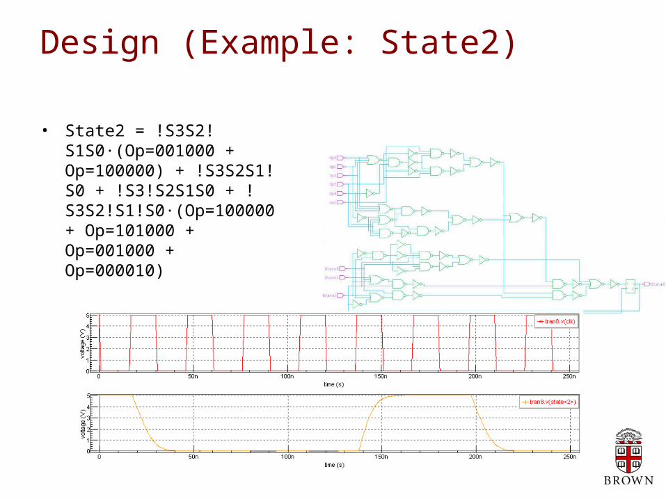
Design (Example: State2)
• State2 = !S3S2!S1S0∙(Op=001000 + Op=100000) + !S3S2S1!S0 + !S3!S2S1S0 + !S3S2!S1!S0∙(Op=100000 + Op=101000 + Op=001000 + Op=000010)

Layout
• Standard Cells: 242• Nets: 254• Length of Nets: 182070.5• Vias: 847• Dimensions: 1187 x 2000• Area: 2,374,0002

Simulation Results
10.813ns
Worst Case (AluSrcB<0>)
6.254ns
Best Case (IRWrite<0>)
Power ≈ 4μW

Wouldn’t It Be Nice…
• If we could draw a state machine diagram and export to a layout program
• If SPICE could simulate faster
• If S-Edit’s library system was better designed for collaboration
• If this could have been done in Verilog, VHDL, or even ABEL
Draw State Diagram
Export as EDIF
Import toS-Edit
Import toL-Edit
Derive 24Logic
Equations
Draw 24+Schematics
Export toVerilog
Covert to EDIF
XXX
X
X
ALU Control Unit and Input Multiplexor
Mike Kadin
EN160

ALU Support Hardware
ReadInput1
ReadInput2
Instr
InstrWriteBack
PC
ALUSrcB ALUSrcA ALUOp

Logic Design
Multiplexors ALU Control Combo Logic
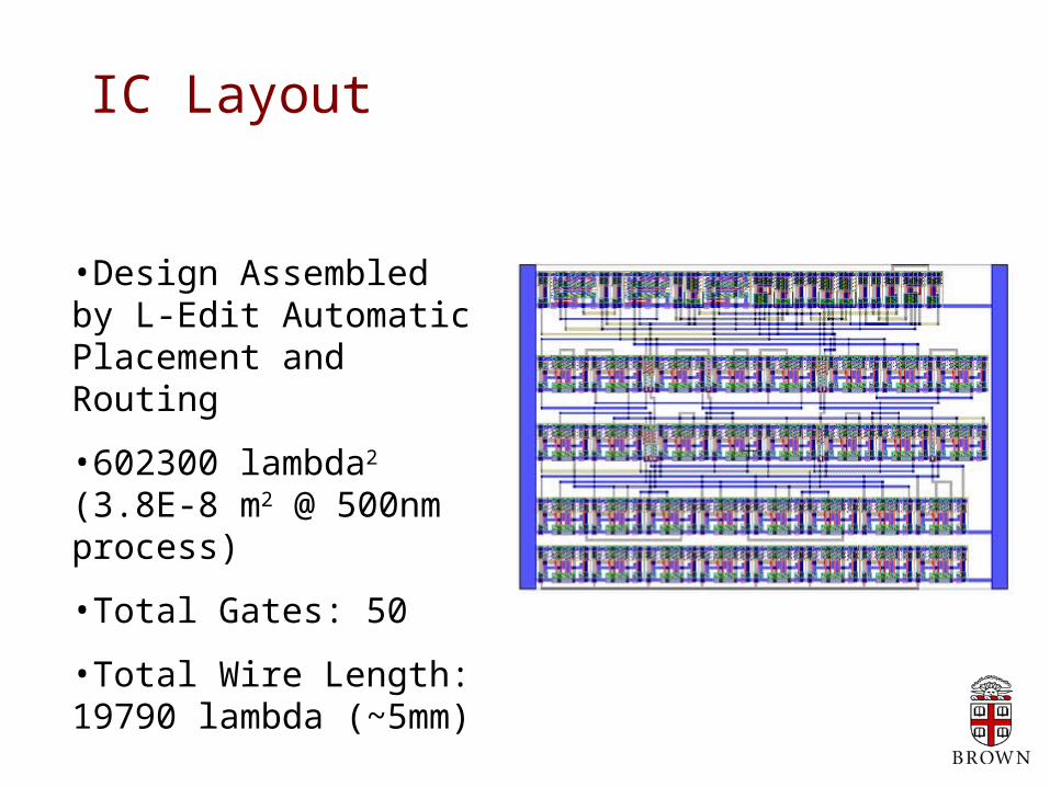
IC Layout
•Design Assembled by L-Edit Automatic Placement and Routing
•602300 lambda2 (3.8E-8 m2 @ 500nm process)
•Total Gates: 50
•Total Wire Length: 19790 lambda (~5mm)
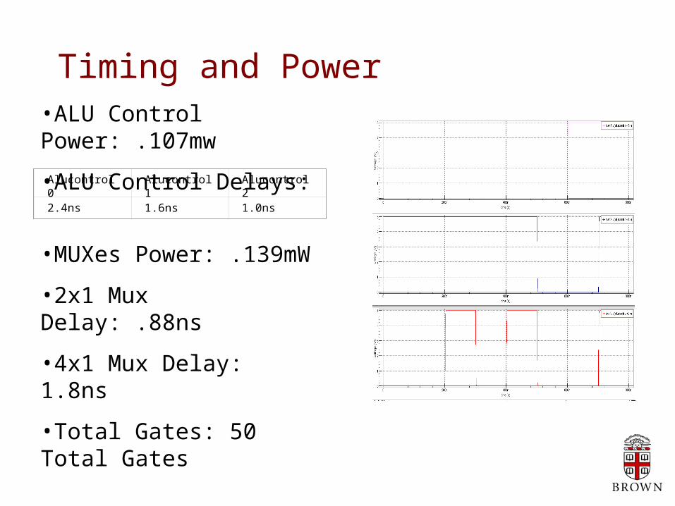
Timing and Power•ALU Control Power: .107mw
•ALU Control Delays:Alucontrol0 Alucontrol1 Alucontrol2
2.4ns 1.6ns 1.0ns
•MUXes Power: .139mW
•2x1 Mux Delay: .88ns
•4x1 Mux Delay: 1.8ns
•Total Gates: 50 Total Gates

Design Problems
• VDD & GND
•2 Inputs from the Same Signal
•Many Inputs Required Much Repeated Typing in the L-Edit Core Setup
•Not Much Room for Creativity In Design

ALU design
Nuno Alves
Yiwen Shi
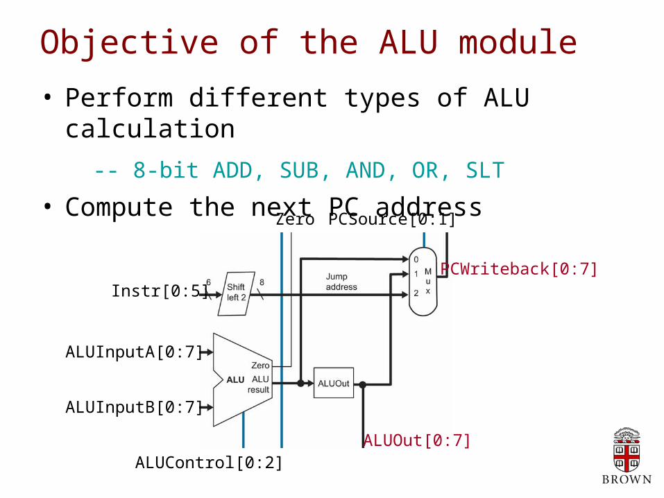
Objective of the ALU module
• Perform different types of ALU calculation
-- 8-bit ADD, SUB, AND, OR, SLT
• Compute the next PC address
Instr[0:5]
ALUOut[0:7]
ALUInputA[0:7]
ALUInputB[0:7]
ALUControl[0:2]
Zero PCSource[0:1]
PCWriteback[0:7]

Logic design 1/2
ALU kernel ADD/SUB module

ALUOut
ShiftLeft2
MUX3
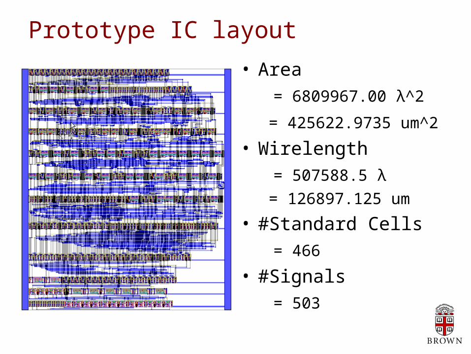
Prototype IC layout
• Area
= 6809967.00 λ^2
= 425622.9735 um^2 • Wirelength
= 507588.5 λ
= 126897.125 um
• #Standard Cells
= 466
• #Signals
= 503
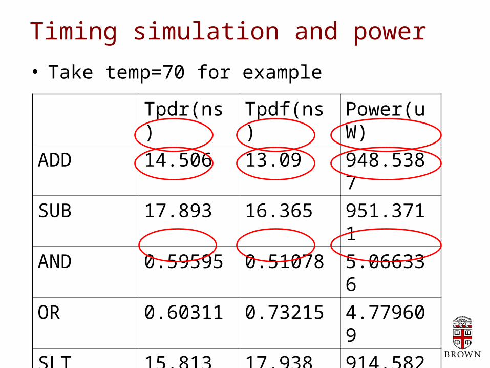
Timing simulation and power
• Take temp=70 for example
Tpdr(ns) Tpdf(ns) Power(uW)
ADD 14.506 13.09 948.5387
SUB 17.893 16.365 951.3711
AND 0.59595 0.51078 5.066336
OR 0.60311 0.73215 4.779609
SLT 15.813 17.938 914.5821
ALUOut 0.9584 0.79592 10.00396
Shifter 0.41479 0.38713 9.457175
MUX3 1.5418 1.3992 5.804854

What we have learned…
• Modularity = smaller designs
• Simulations agree with theoretical results
• It is unfortunate than S-Edit, L-Edit and Spice are not combined into a single package
• Very hard to debug schematics in S-Edit

Register File
Luis Camacho

Register File Module
• Reads up to 2 register (same time)• Writes into a destination register• Uses (8) 8-bit registers• (8) I/O pins
WRITE ENABLE
READREG 1
READREG 2
WRITEREGISTER
DATA
READDATA 1
READDATA 2
CLK
A
B

8-bit Register 8x8 Multiplexer
Register File Schematic
Enable write destination register

3x8 Decoder
8-bit Register
D Q
Q’
CLK
1 0 1 0 1 0 1 0 1 1 0 0 1 1 0 0 1 1 1 1 0 0 0 0
Timing Simulations

8x8 Multiplexer
Timing Simulations
R$0R$1R$2R$3R$4R$5R$6R$7
Out[0:7]
Add[0:2]
10101010
100

INPUT: 10101010 READ R$0 READ R$1
Register File - Timing Simulation
[13-18ns] [6-11ns] [9-10ns]

Layout Analysis
Area : 739.375μmx1.13mm
Write-Read Cycle:
[13-18ns]
Wirelength = 30cm Read delay ≈ 9ns
#vias = 3119 Write delay ≈ 6ns
cells = 585 Power = 6.295 mW
#nets = 660

Comments
Lessons learnt:
• Tristate buffer vs Multiplexer• Performance of SmartSpice vs T-Spice• Alternative way to ground Register 0
Things that could have speed up simulations:
• Feature to connect ports (one-to-many)• Better way to export SmartView figures

Integration
Brian Reggiannini

CPU Floorplan
PCAddress
GeneratorAddr[7:0]
Control FSM
RE
SE
T
Mem
Write
Mem
Read
ALU WriteData[7:0]
Register File MemData[7:0]
ALU Control
IorD PC
En
PCWriteBack[7:0]
Zero
PC
Source
ALUInputA[7:0]
ALUInputB[7:0]
ALUControl[2:0]
ALU
SrcA
ALU
SrcB
[1:0]
ALU
Op[1:0]
Op[5:0]
IRWrite
RegDst
RegWrite
MemtoRegR
eadData2[7:0]
ReadD
ata1[7:0]
PC[7:0]
ALUOutput[7:0]
ALU
Output[7:0]
Instr[5:0]
Instr[7:0]
Instr[7:0]


Layout
• Area– Total area 4234.5 x 6555.0 λ2
– λ = 250 nm– Total area 1.73 mm2
• 1346 standard cells
• Wire Length– 2305973.5 λ = 57.6 cm

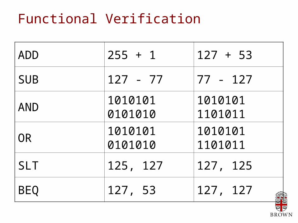
Functional Verification
ADD 255 + 1 127 + 53
SUB 127 - 77 77 - 127
AND1010101 0101010
1010101 1101011
OR1010101 0101010
1010101 1101011
SLT 125, 127 127, 125
BEQ 127, 53 127, 127
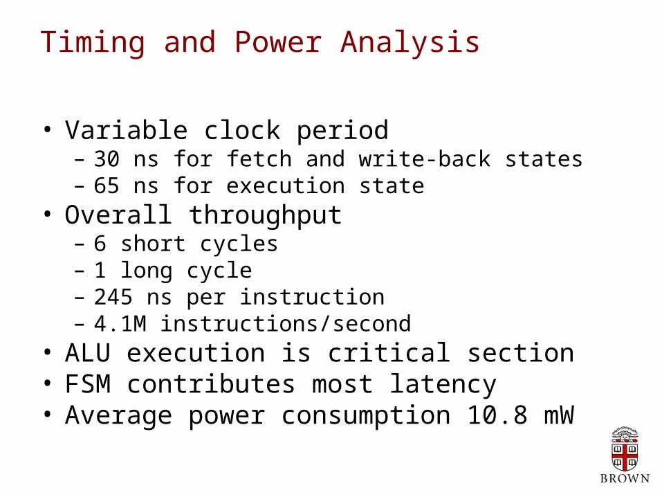
Timing and Power Analysis
• Variable clock period– 30 ns for fetch and write-back states– 65 ns for execution state
• Overall throughput– 6 short cycles– 1 long cycle– 245 ns per instruction– 4.1M instructions/second
• ALU execution is critical section• FSM contributes most latency• Average power consumption 10.8 mW