Embed Size (px)
Citation preview
S4103N-channel SiC power MOSFET bare die
VDSS 1200V
RDS(on) (Typ.) 22mW
ID 95A*1
・Switch mode power supplies
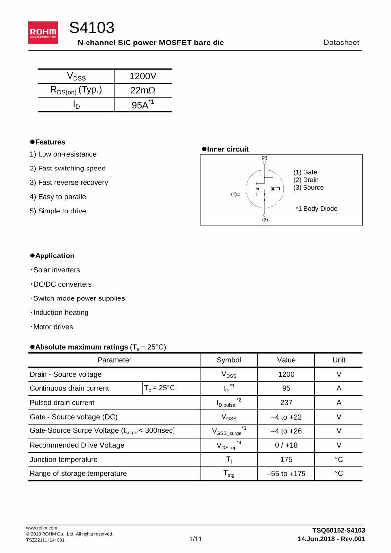
lFeatureslInner circuit
1) Low on-resistance
2) Fast switching speed
3) Fast reverse recovery
4) Easy to parallel
5) Simple to drive
lApplication
・Solar inverters
・DC/DC converters
・Induction heating
・Motor drives
lAbsolute maximum ratings (Ta = 25°C)
Parameter Symbol
Continuous drain current Tc = 25°C ID *1 95 A
Unit
Drain - Source voltage VDSS 1200 V
Value
Pulsed drain current ID,pulse *2 237 A
Gate - Source voltage (DC) VGSS -4 to +22 V
Junction temperature Tj 175 °C
Range of storage temperature Tstg -55 to +175 °C
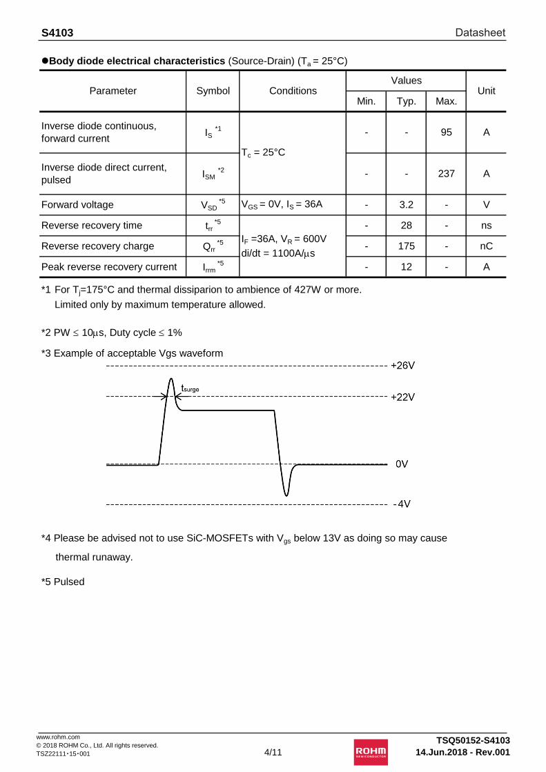
Gate-Source Surge Voltage (tsurge < 300nsec) VGSS_surge*3
-4 to +26 V
Recommended Drive Voltage VGS_op*4 0 / +18 V
(1) Gate (2) Drain (3) Source
*1 Body Diode
www.rohm.com
© 2018 ROHM Co., Ltd. All rights reserved.
TSZ22111・14・001 1/11
TSQ50152-S4103
14.Jun.2018 - Rev.001
Datasheet
S4103
UnitMin. Typ. Max.
lElectrical characteristics (Ta = 25°C)
Parameter Symbol ConditionsValues
V
Zero gate voltage
drain currentIDSS
VDS = 1200V, VGS = 0V
mATj = 25°C -
Drain - Source breakdown
voltageV(BR)DSS VGS = 0V, ID = 1mA 1200 - -
1 10
Tj = 150°C - 2 -
Gate - Source leakage current IGSS+ VGS = +22V, VDS = 0V - - 100 nA
Gate - Source leakage current IGSS- VGS = -4V, VDS = 0V - - -100 nA
5.6 V
Static drain - source
on - state resistanceRDS(on)
*5
VGS = 18V, ID = 36A
mWTj = 25°C
Gate threshold voltage VGS (th) VDS = 10V, ID = 18.2mA 2.7 -
- 22 27.5
Tj = 125°C - 33 -
WGate input resistance RG f = 1MHz, open drain - 4 -
www.rohm.com
© 2018 ROHM Co., Ltd. All rights reserved.
TSZ22111・15・001 2/11
TSQ50152-S4103
14.Jun.2018 - Rev.001
Datasheet
S4103
lElectrical characteristics (Ta = 25°C)
Parameter Symbol ConditionsValues
UnitMin. Typ. Max.
S
Input capacitance Ciss VGS = 0V - 2879 -
pFOutput capacitance Coss
Transconductance gfs *5 VDS = 10V, ID = 36A - 14.2 -
VDS = 800V - 237 -
Reverse transfer capacitance Crss f = 1MHz - 108 -
pF
Turn - on delay time td(on) *5 VDD = 400V, ID = 18A - 29 -
nsRise time
Effective output capacitance,
energy relatedCo(er)
VGS = 0V
VDS = 0V to 600V- 213 -
-
Fall time tf *5 RG = 0W - 28 -
tr *5 VGS = 18V/0V - 44 -
Turn - off delay time td(off) *5 RL = 22W - 67
mJ
Turn - off switching loss Eoff *5 - 243 -
Turn - on switching loss Eon *5 VDD = 600V, ID=36A
VGS = 18V/0V
RG = 0W L=250mH
*Eon includes diode
reverse recovery
- 632 -
- 178 -
lGate Charge characteristics (Ta = 25°C)
Parameter Symbol ConditionsValues
UnitMin. Typ. Max.
V
- 80 -
Gate plateau voltage V(plateau) VDD = 600V, ID = 36A - 9.6 -
nCGate - Source charge Qgs *5 ID = 36A - 40 -
Gate - Drain charge Qgd *5 VGS = 18V
Total gate charge Qg *5 VDD = 600V
www.rohm.com
© 2018 ROHM Co., Ltd. All rights reserved.
TSZ22111・15・001 3/11
TSQ50152-S4103
14.Jun.2018 - Rev.001
Datasheet
S4103
lBody diode electrical characteristics (Source-Drain) (Ta = 25°C)
*1 Limited only by maximum temperature allowed.For Tj=175°C and thermal dissiparion to ambience of 427W or more.
Limited only by maximum temperature allowed.
*2 PW 10ms, Duty cycle 1%
*3 Example of acceptable Vgs waveform
*4 Please be advised not to use SiC-MOSFETs with Vgs below 13V as doing so may cause
thermal runaway.
*5 Pulsed
Parameter Symbol ConditionsValues
UnitMin. Typ. Max.
A
Inverse diode direct current,
pulsedISM
*2 - - 237 A
Inverse diode continuous,
forward currentIS
*1
Tc = 25°C
- - 95
V
Reverse recovery time trr *5
IF =36A, VR = 600V
di/dt = 1100A/ms
- 28 - ns
Reverse recovery charge
Forward voltage VSD *5 VGS = 0V, IS = 36A - 3.2 -
Peak reverse recovery current Irrm *5
- 12 - A
Qrr *5 - 175 - nC
www.rohm.com
© 2018 ROHM Co., Ltd. All rights reserved.
TSZ22111・15・001 4/11
TSQ50152-S4103
14.Jun.2018 - Rev.001
Datasheet
S4103
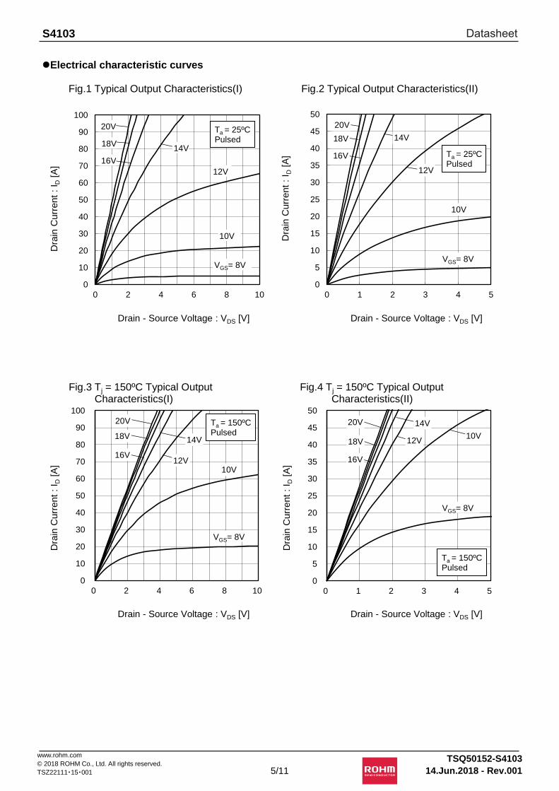
lElectrical characteristic curves
Fig.1 Typical Output Characteristics(I)
Dra
in C
urr
ent
: I D
[A
]
Drain - Source Voltage : VDS [V]
Fig.2 Typical Output Characteristics(II)
Drain - Source Voltage : VDS [V]
Fig.3 Tj = 150ºC Typical Output Characteristics(I)
Dra
in C
urr
ent
: I D
[A
]
Drain - Source Voltage : VDS [V]
Fig.4 Tj = 150ºC Typical Output Characteristics(II)
Dra
in C
urr
ent
: I D
[A
]
Drain - Source Voltage : VDS [V]
Dra
in C
urr
ent
: I D
[A
] 0
10
20
30
40
50
60
70
80
90
100
0 2 4 6 8 10
Ta = 25ºC Pulsed
10V
VGS= 8V
12V
16V
20V
18V 14V
0
5
10
15
20
25
30
35
40
45
50
0 1 2 3 4 5
Ta = 25ºC Pulsed
VGS= 8V
10V
14V
16V
18V
20V
12V
0
10
20
30
40
50
60
70
80
90
100
0 2 4 6 8 10
Ta = 150ºC Pulsed
10V
VGS= 8V
18V
16V
20V
14V
12V
0
5
10
15
20
25
30
35
40
45
50
0 1 2 3 4 5
Ta = 150ºC Pulsed
VGS= 8V
18V
16V
14V
12V
20V
10V
www.rohm.com
© 2018 ROHM Co., Ltd. All rights reserved.
TSZ22111・15・001 5/11
TSQ50152-S4103
14.Jun.2018 - Rev.001
Datasheet
S4103
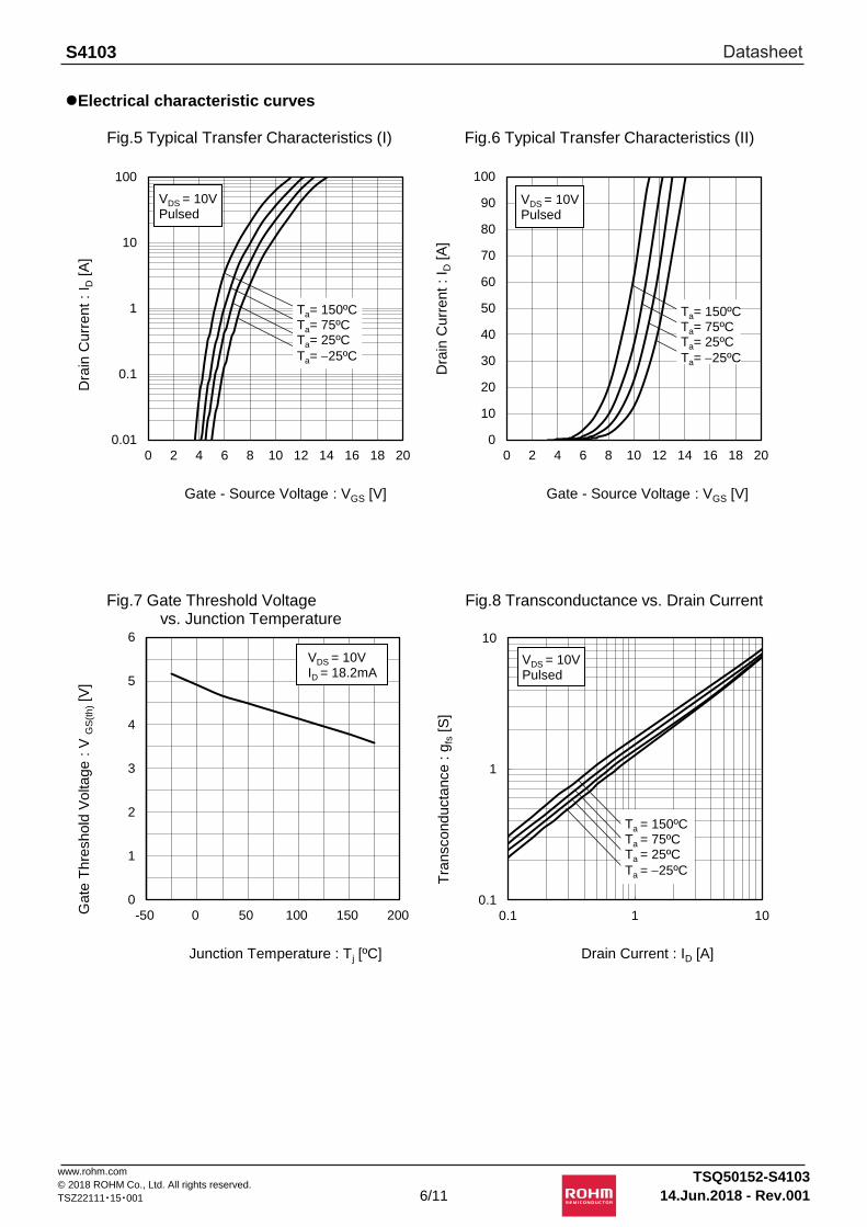
lElectrical characteristic curves
Fig.5 Typical Transfer Characteristics (I)
Dra
in C
urr
ent
: I D
[A
]
Gate - Source Voltage : VGS [V]
Fig.6 Typical Transfer Characteristics (II)
Gate - Source Voltage : VGS [V]
Fig.7 Gate Threshold Voltage vs. Junction Temperature
Gate
Thre
shold
Voltage :
V G
S(t
h) [V
]
Junction Temperature : Tj [ºC]
Fig.8 Transconductance vs. Drain Current
Tra
nsconducta
nce :
gfs [S
]
Drain Current : ID [A]
Dra
in C
urr
ent
: I D
[A
]
0.1
1
10
0.1 1 10
VDS = 10V Pulsed
Ta = 150ºC Ta = 75ºC Ta = 25ºC
Ta = -25ºC
0
1
2
3
4
5
6
-50 0 50 100 150 200
VDS = 10V ID = 18.2mA
0.01
0.1
1
10
100
0 2 4 6 8 10 12 14 16 18 20
Ta= 150ºC Ta= 75ºC Ta= 25ºC
Ta= -25ºC
VDS = 10V Pulsed
0
10
20
30
40
50
60
70
80
90
100
0 2 4 6 8 10 12 14 16 18 20
Ta= 150ºC Ta= 75ºC Ta= 25ºC
Ta= -25ºC
VDS = 10V Pulsed
www.rohm.com
© 2018 ROHM Co., Ltd. All rights reserved.
TSZ22111・15・001 6/11
TSQ50152-S4103
14.Jun.2018 - Rev.001
Datasheet
S4103
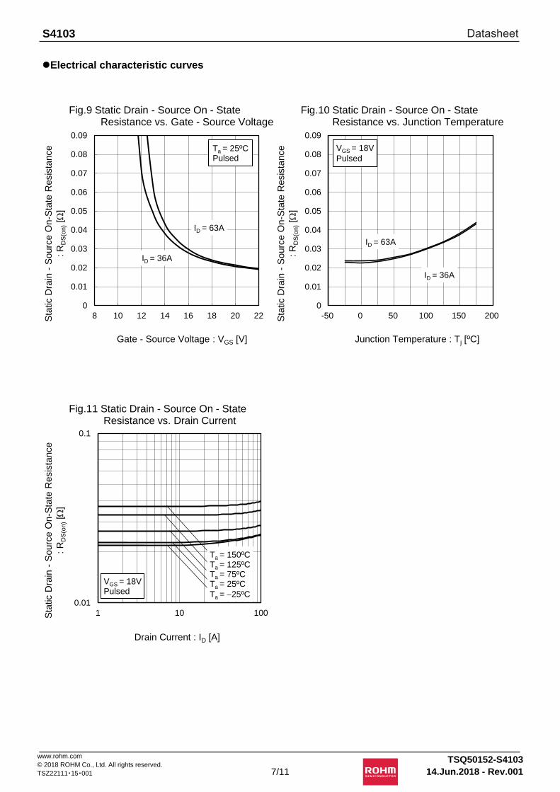
lElectrical characteristic curves
Fig.9 Static Drain - Source On - State Resistance vs. Gate - Source Voltage
Sta
tic D
rain
- S
ourc
e O
n-S
tate
Resis
tance
: R
DS
(on) [W
]
Gate - Source Voltage : VGS [V]
Fig.10 Static Drain - Source On - State Resistance vs. Junction Temperature
Junction Temperature : Tj [ºC]
Fig.11 Static Drain - Source On - State Resistance vs. Drain Current
Drain Current : ID [A]
Sta
tic D
rain
- S
ourc
e O
n-S
tate
Resis
tance
: R
DS
(on) [W
]
Sta
tic D
rain
- S
ourc
e O
n-S
tate
Resis
tance
: R
DS
(on) [W
]
0
0.01
0.02
0.03
0.04
0.05
0.06
0.07
0.08
0.09
8 10 12 14 16 18 20 22
ID = 36A
ID = 63A
Ta = 25ºC Pulsed
0
0.01
0.02
0.03
0.04
0.05
0.06
0.07
0.08
0.09
-50 0 50 100 150 200
VGS = 18V
Pulsed
ID = 63A
ID = 36A
0.01
0.1
1 10 100
VGS = 18V Pulsed
Ta = 150ºC Ta = 125ºC Ta = 75ºC Ta = 25ºC
Ta = -25ºC
www.rohm.com
© 2018 ROHM Co., Ltd. All rights reserved.
TSZ22111・15・001 7/11
TSQ50152-S4103
14.Jun.2018 - Rev.001
Datasheet
S4103
lElectrical characteristic curves
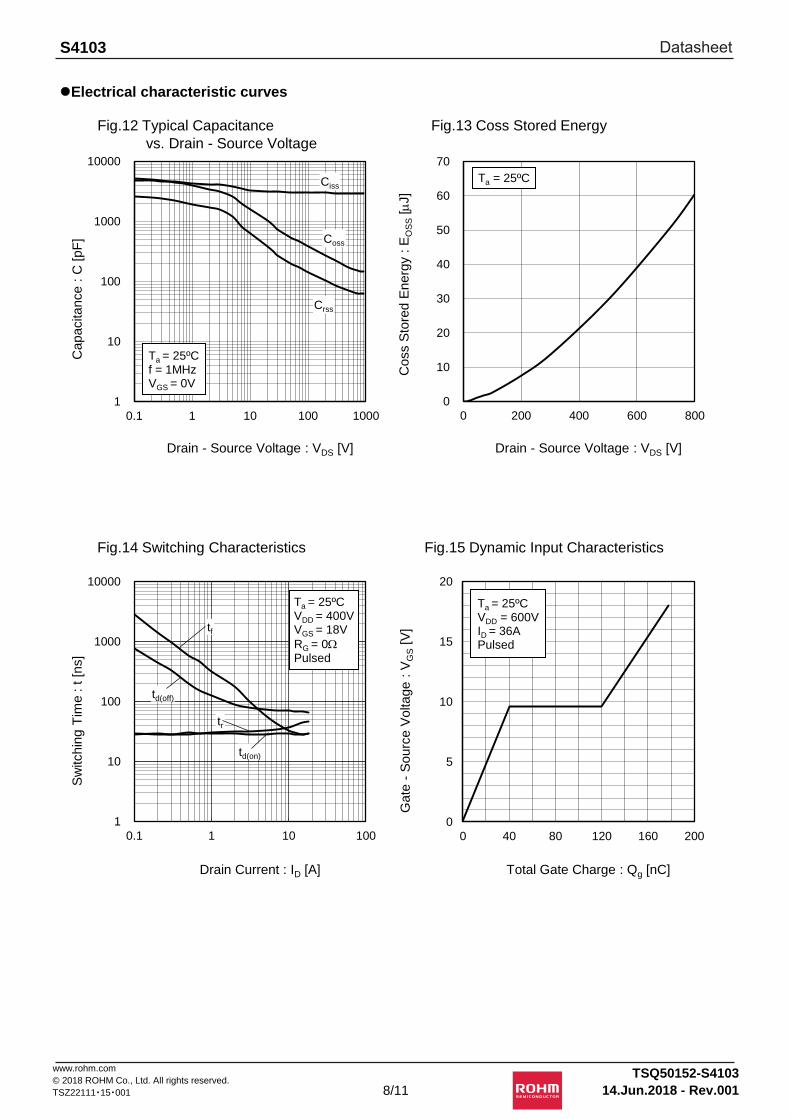
Fig.12 Typical Capacitance
vs. Drain - Source Voltage
Capacitance :
C [pF
]
Drain - Source Voltage : VDS [V]
Fig.13 Coss Stored Energy
Drain - Source Voltage : VDS [V]
Fig.14 Switching Characteristics
Sw
itchin
g T
ime : t [
ns]
Drain Current : ID [A]
Fig.15 Dynamic Input Characteristics
Gate
- S
ourc
e V
oltage :
VG
S [V
]
Total Gate Charge : Qg [nC]
Coss S
tore
d E
nerg
y : E
OS
S [
mJ]
0
10
20
30
40
50
60
70
0 200 400 600 800
Ta = 25ºC
1
10
100
1000
10000
0.1 1 10 100 1000
Ciss
Coss
Crss
Ta = 25ºC f = 1MHz VGS = 0V
0
5
10
15
20
0 40 80 120 160 200
Ta = 25ºC VDD = 600V ID = 36A Pulsed
1
10
100
1000
10000
0.1 1 10 100
td(on)
td(off)
Ta = 25ºC VDD = 400V VGS = 18V
RG = 0W
Pulsed
tr
tf
www.rohm.com
© 2018 ROHM Co., Ltd. All rights reserved.
TSZ22111・15・001 8/11
TSQ50152-S4103
14.Jun.2018 - Rev.001
Datasheet
S4103
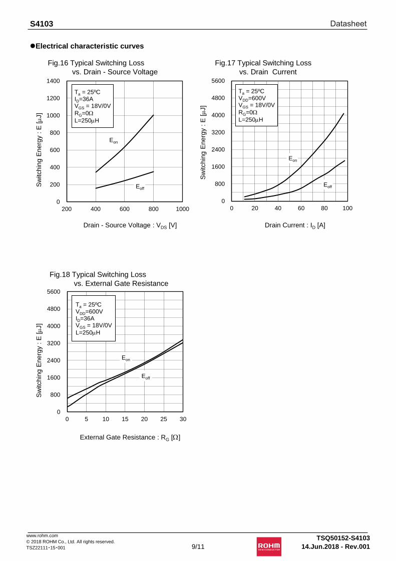
lElectrical characteristic curves
Fig.16 Typical Switching Loss
vs. Drain - Source Voltage
Sw
itchin
g E
nerg
y : E
[mJ]
Drain - Source Voltage : VDS [V]
Fig.17 Typical Switching Loss
vs. Drain Current
Drain Current : ID [A]
Fig.18 Typical Switching Loss
vs. External Gate Resistance
Sw
itchin
g E
nerg
y : E
[mJ]
External Gate Resistance : RG [W]
Sw
itchin
g E
nerg
y : E
[mJ]
0
800
1600
2400
3200
4000
4800
5600
0 20 40 60 80 100
Ta = 25ºC VDD=600V VGS = 18V/0V
RG=0W
L=250mH
Eon
Eoff
0
200
400
600
800
1000
1200
1400
200 400 600 800 1000
Ta = 25ºC ID=36A VGS = 18V/0V
RG=0W
L=250mH
Eon
Eoff
0
800
1600
2400
3200
4000
4800
5600
0 5 10 15 20 25 30
Ta = 25ºC VDD=600V ID=36A VGS = 18V/0V
L=250mH
Eon
Eoff
www.rohm.com
© 2018 ROHM Co., Ltd. All rights reserved.
TSZ22111・15・001 9/11
TSQ50152-S4103
14.Jun.2018 - Rev.001
Datasheet
S4103
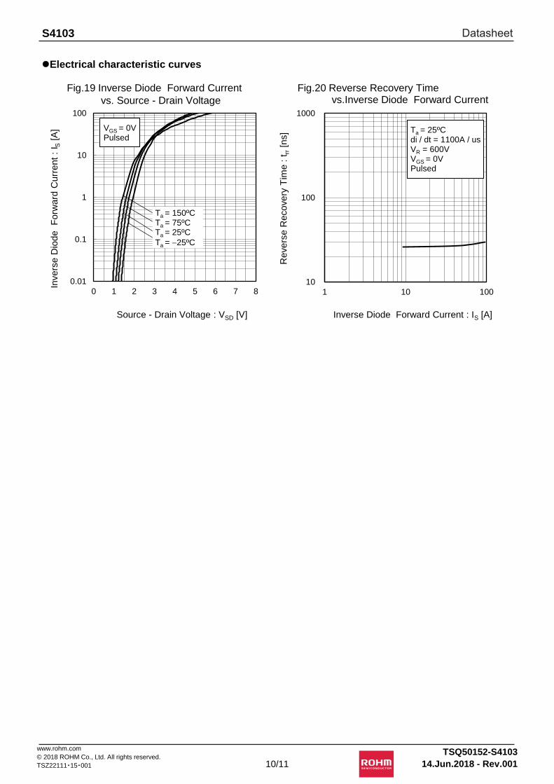
lElectrical characteristic curves
Fig.19 Inverse Diode Forward Current
vs. Source - Drain Voltage
Invers
e D
iode
Forw
ard
Curr
ent
: I S
[A
]
Source - Drain Voltage : VSD [V]
Fig.20 Reverse Recovery Time vs.Inverse Diode Forward Current
Inverse Diode Forward Current : IS [A]
Revers
e R
ecovery
Tim
e : t
rr [ns]
0.01
0.1
1
10
100
0 1 2 3 4 5 6 7 8
VGS = 0V Pulsed
Ta = 150ºC Ta = 75ºC Ta = 25ºC
Ta = -25ºC
10
100
1000
1 10 100
Ta = 25ºC di / dt = 1100A / us VR = 600V VGS = 0V Pulsed
www.rohm.com
© 2018 ROHM Co., Ltd. All rights reserved.
TSZ22111・15・001 10/11
TSQ50152-S4103
14.Jun.2018 - Rev.001
Datasheet

S4103
lMeasurement circuits
Fig.1-1 Switching Time Measurement Circuit Fig.1-2 Switching Waveforms
Fig.2-1 Gate Charge Measurement Circuit Fig.2-2 Gate Charge Waveform
Fig.3-1 Switching Energy Measurement Circuit Fig.3-2 Switching Waveforms
Fig.4-1 Reverse Recovery Time Measurement Circuit Fig.4-2 Reverse Recovery Waveform
D.U.T.
Vsurge Irr
Eon = ID×VDS Eoff = ID×VDS
ID
VDS
Same type device as
D.U.T.
D.U.T.
ID
www.rohm.com
© 2018 ROHM Co., Ltd. All rights reserved.
TSZ22111・15・001 11/11
TSQ50152-S4103
14.Jun.2018 - Rev.001
Datasheet
R1102Swww.rohm.com© 2015 ROHM Co., Ltd. All rights reserved.
Notice
ROHM Customer Support System http://www.rohm.com/contact/
Thank you for your accessing to ROHM product informations. More detail product informations and catalogs are available, please contact us.
N o t e s
The information contained herein is subject to change without notice.
Before you use our Products, please contact our sales representative and verify the latest specifica-tions :
Although ROHM is continuously working to improve product reliability and quality, semicon-ductors can break down and malfunction due to various factors.Therefore, in order to prevent personal injury or fire arising from failure, please take safety measures such as complying with the derating characteristics, implementing redundant and fire prevention designs, and utilizing backups and fail-safe procedures. ROHM shall have no responsibility for any damages arising out of the use of our Poducts beyond the rating specified by ROHM.
Examples of application circuits, circuit constants and any other information contained herein are provided only to illustrate the standard usage and operations of the Products. The peripheral conditions must be taken into account when designing circuits for mass production.
The technical information specified herein is intended only to show the typical functions of and examples of application circuits for the Products. ROHM does not grant you, explicitly or implicitly, any license to use or exercise intellectual property or other rights held by ROHM or any other parties. ROHM shall have no responsibility whatsoever for any dispute arising out of the use of such technical information.
The Products specified in this document are not designed to be radiation tolerant.
For use of our Products in applications requiring a high degree of reliability (as exemplified below), please contact and consult with a ROHM representative : transportation equipment (i.e. cars, ships, trains), primary communication equipment, traffic lights, fire/crime prevention, safety equipment, medical systems, and power transmission systems.
Do not use our Products in applications requiring extremely high reliability, such as aerospace equipment, nuclear power control systems, and submarine repeaters.
ROHM shall have no responsibility for any damages or injury arising from non-compliance with the recommended usage conditions and specifications contained herein.
ROHM has used reasonable care to ensur the accuracy of the information contained in this document. However, ROHM does not warrants that such information is error-free, and ROHM shall have no responsibility for any damages arising from any inaccuracy or misprint of such information.
Please use the Products in accordance with any applicable environmental laws and regulations, such as the RoHS Directive. For more details, including RoHS compatibility, please contact a ROHM sales office. ROHM shall have no responsibility for any damages or losses resulting non-compliance with any applicable laws or regulations.
When providing our Products and technologies contained in this document to other countries, you must abide by the procedures and provisions stipulated in all applicable export laws and regulations, including without limitation the US Export Administration Regulations and the Foreign Exchange and Foreign Trade Act.
This document, in part or in whole, may not be reprinted or reproduced without prior consent of ROHM.
1)
2)
3)
4)
5)
6)
7)
8)
9)
10)
11)
12)
13)