Embed Size (px)
Citation preview

Datasheet
www.renesas.com
S7G2 Microcontroller Group
Datasheet
Renesas Synergy™ PlatformSynergy MicrocontrollersS7 Series
Jan 2018Rev.1.30
All information contained in these materials, including products and product specifications,represents information on the product at the time of publication and is subject to change byRenesas Electronics Corp. without notice. Please review the latest information published byRenesas Electronics Corp. through various means, including the Renesas Electronics Corp.website (http://www.renesas.com).
Cover
R01DS0262EU0130 Rev.1.30 Page 2 of 122Jan 3, 2018
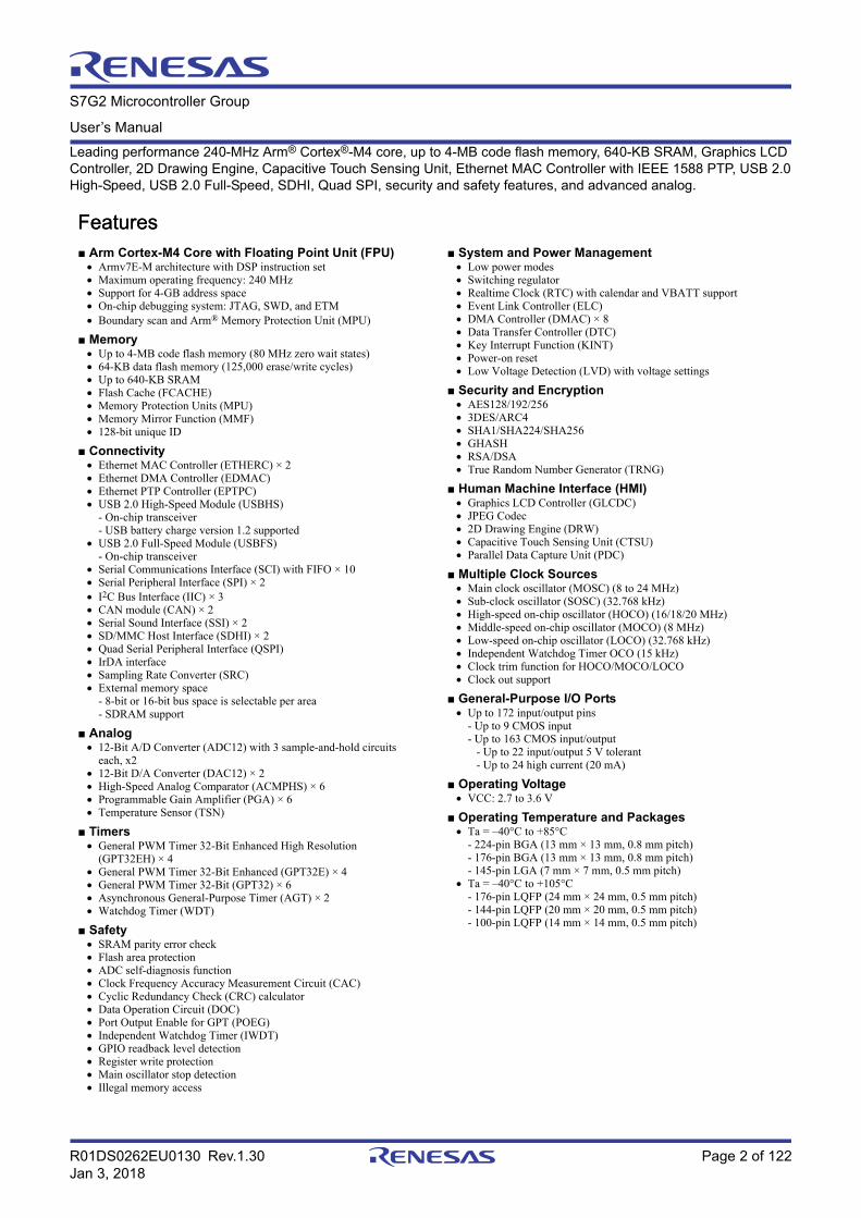
Features Arm Cortex-M4 Core with Floating Point Unit (FPU) Armv7E-M architecture with DSP instruction set Maximum operating frequency: 240 MHz Support for 4-GB address space On-chip debugging system: JTAG, SWD, and ETM Boundary scan and Arm® Memory Protection Unit (MPU)
Memory Up to 4-MB code flash memory (80 MHz zero wait states) 64-KB data flash memory (125,000 erase/write cycles) Up to 640-KB SRAM Flash Cache (FCACHE) Memory Protection Units (MPU) Memory Mirror Function (MMF) 128-bit unique ID
Connectivity Ethernet MAC Controller (ETHERC) × 2 Ethernet DMA Controller (EDMAC) Ethernet PTP Controller (EPTPC) USB 2.0 High-Speed Module (USBHS)
- On-chip transceiver- USB battery charge version 1.2 supported
USB 2.0 Full-Speed Module (USBFS)- On-chip transceiver
Serial Communications Interface (SCI) with FIFO × 10 Serial Peripheral Interface (SPI) × 2 I2C Bus Interface (IIC) × 3 CAN module (CAN) × 2 Serial Sound Interface (SSI) × 2 SD/MMC Host Interface (SDHI) × 2 Quad Serial Peripheral Interface (QSPI) IrDA interface Sampling Rate Converter (SRC) External memory space
- 8-bit or 16-bit bus space is selectable per area- SDRAM support
Analog 12-Bit A/D Converter (ADC12) with 3 sample-and-hold circuits
each, x2 12-Bit D/A Converter (DAC12) × 2 High-Speed Analog Comparator (ACMPHS) × 6 Programmable Gain Amplifier (PGA) × 6 Temperature Sensor (TSN)
Timers General PWM Timer 32-Bit Enhanced High Resolution
(GPT32EH) × 4 General PWM Timer 32-Bit Enhanced (GPT32E) × 4 General PWM Timer 32-Bit (GPT32) × 6 Asynchronous General-Purpose Timer (AGT) × 2 Watchdog Timer (WDT)
Safety SRAM parity error check Flash area protection ADC self-diagnosis function Clock Frequency Accuracy Measurement Circuit (CAC) Cyclic Redundancy Check (CRC) calculator Data Operation Circuit (DOC) Port Output Enable for GPT (POEG) Independent Watchdog Timer (IWDT) GPIO readback level detection Register write protection Main oscillator stop detection Illegal memory access
System and Power Management Low power modes Switching regulator Realtime Clock (RTC) with calendar and VBATT support Event Link Controller (ELC) DMA Controller (DMAC) × 8 Data Transfer Controller (DTC) Key Interrupt Function (KINT) Power-on reset Low Voltage Detection (LVD) with voltage settings
Security and Encryption AES128/192/256 3DES/ARC4 SHA1/SHA224/SHA256 GHASH RSA/DSA True Random Number Generator (TRNG)
Human Machine Interface (HMI) Graphics LCD Controller (GLCDC) JPEG Codec 2D Drawing Engine (DRW) Capacitive Touch Sensing Unit (CTSU) Parallel Data Capture Unit (PDC)
Multiple Clock Sources Main clock oscillator (MOSC) (8 to 24 MHz) Sub-clock oscillator (SOSC) (32.768 kHz) High-speed on-chip oscillator (HOCO) (16/18/20 MHz) Middle-speed on-chip oscillator (MOCO) (8 MHz) Low-speed on-chip oscillator (LOCO) (32.768 kHz) Independent Watchdog Timer OCO (15 kHz) Clock trim function for HOCO/MOCO/LOCO Clock out support
General-Purpose I/O Ports Up to 172 input/output pins
- Up to 9 CMOS input- Up to 163 CMOS input/output - Up to 22 input/output 5 V tolerant - Up to 24 high current (20 mA)
Operating Voltage VCC: 2.7 to 3.6 V
Operating Temperature and Packages Ta = –40°C to +85°C
- 224-pin BGA (13 mm × 13 mm, 0.8 mm pitch)- 176-pin BGA (13 mm × 13 mm, 0.8 mm pitch)- 145-pin LGA (7 mm × 7 mm, 0.5 mm pitch)
Ta = –40°C to +105°C- 176-pin LQFP (24 mm × 24 mm, 0.5 mm pitch)- 144-pin LQFP (20 mm × 20 mm, 0.5 mm pitch)- 100-pin LQFP (14 mm × 14 mm, 0.5 mm pitch)
Leading performance 240-MHz Arm® Cortex®-M4 core, up to 4-MB code flash memory, 640-KB SRAM, Graphics LCD Controller, 2D Drawing Engine, Capacitive Touch Sensing Unit, Ethernet MAC Controller with IEEE 1588 PTP, USB 2.0 High-Speed, USB 2.0 Full-Speed, SDHI, Quad SPI, security and safety features, and advanced analog.
S7G2 Microcontroller Group
User’s Manual
Features
R01DS0262EU0130 Rev.1.30 Page 3 of 122Jan 3, 2018
S7G2 Datasheet 1. Overview
1. OverviewThe MCU integrates multiple series of software- and pin-compatible Arm®-based 32-bit MCUs that share the same set of Renesas peripherals to facilitate design scalability and efficient platform-based product development.
The MCU provides a high-performance Arm Cortex®-M4 core running up to 240 MHz with the following features:
Up to 4-MB code flash memory
640-KB SRAM
Graphics LCD Controller (GLCDC)
2D Drawing Engine (DRW)
Capacitive Touch Sensing Unit (CTSU)
Ethernet MAC Controller (ETHERC) with IEEE 1588 PTP, USBFS, USBHS, SD/MMC Host Interface
Quad Serial Peripheral Interface (QSPI)
Security and safety features
Analog peripherals.
1.1 Function Outline
Table 1.1 Arm core
Feature Functional description
Arm Cortex-M4 Maximum operating frequency: up to 240 MHz Arm Cortex-M4 core:
- Revision: r0p1-01rel0- Armv7E-M architecture profile- Single precision floating point unit compliant with the ANSI/IEEE Std 754-2008
Arm Memory Protection Unit (MPU):- Armv7 Protected Memory System Architecture- 8 protect regions
SysTick timer:- Driven by SYSTICCLK (LOCO) or ICLK.
Table 1.2 Memory
Feature Functional description
Code flash memory Maximum 4 MB of code flash memory. See section 54, Flash Memory in User’s Manual.
Data flash memory 64 KB of data flash memory. See section 54, Flash Memory in User’s Manual.
Option-setting memory The option-setting memory determines the state of the MCU after a reset. See section 7, Option-Setting Memory in User’s Manual.
Memory Mirror Function (MMF) The MMF can be configured to mirror the wanted application image load address in code flash memory to the application image link address in the 23-bit unused memory space (memory mirror space addresses). Your application code is developed and linked to run from this MMF destination address. The application code does not need to know the load location where it is stored in code flash memory. See section 5, Memory Mirror Function (MMF) in User’s Manual.
SRAM On-chip high-speed SRAM providing either parity-bit or double-bit error detection (DED). The first 32 KB of SRAM0 is subject to DED. Parity check is performed for other areas. See section 52, SRAM in User’s Manual.
Standby SRAM On-chip SRAM that can retain data in Deep Software Standby mode. See section 53, Standby SRAM in User’s Manual.
R01DS0262EU0130 Rev.1.30 Page 4 of 122Jan 3, 2018
S7G2 Datasheet 1. Overview
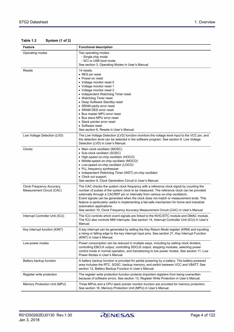
Table 1.3 System (1 of 2)
Feature Functional description
Operating modes Two operating modes: - Single-chip mode - SCI or USB boot mode.See section 3, Operating Modes in User’s Manual.
Resets 14 resets: RES pin reset Power-on reset Voltage monitor reset 0 Voltage monitor reset 1 Voltage monitor reset 2 Independent Watchdog Timer reset Watchdog Timer reset Deep Software Standby reset SRAM parity error reset SRAM DED error reset Bus master MPU error reset Bus slave MPU error reset Stack pointer error reset Software reset.See section 6, Resets in User’s Manual.
Low Voltage Detection (LVD) The Low Voltage Detection (LVD) function monitors the voltage level input to the VCC pin, and the detection level can be selected in the software program. See section 8, Low Voltage Detection (LVD) in User’s Manual.
Clocks Main clock oscillator (MOSC) Sub-clock oscillator (SOSC) High-speed on-chip oscillator (HOCO) Middle-speed on-chip oscillator (MOCO) Low-speed on-chip oscillator (LOCO) PLL frequency synthesizer Independent Watchdog Timer (WDT) on-chip oscillator Clock out support.See section 9, Clock Generation Circuit in User’s Manual.
Clock Frequency Accuracy Measurement Circuit (CAC)
The CAC checks the system clock frequency with a reference clock signal by counting the number of pulses of the system clock to be measured. The reference clock can be provided externally through a CACREF pin or internally from various on-chip oscillators.Event signals can be generated when the clock does not match or measurement ends. This feature is particularly useful in implementing a fail-safe mechanism for home and industrial automation applications.See section 10, Clock Frequency Accuracy Measurement Circuit (CAC) in User’s Manual.
Interrupt Controller Unit (ICU) The ICU controls which event signals are linked to the NVIC/DTC module and DMAC module. The ICU also controls NMI interrupts. See section 14, Interrupt Controller Unit (ICU) in User’s Manual.
Key interrupt function (KINT) A key interrupt can be generated by setting the Key Return Mode register (KRM) and inputting a rising or falling edge to the key interrupt input pins. See section 21, Key Interrupt Function (KINT) in User’s Manual.
Low-power modes Power consumption can be reduced in multiple ways, including by setting clock dividers, controlling EBCLK output, controlling SDCLK output, stopping modules, selecting power control mode in normal operation, and transitioning to low power modes. See section 11, Low Power Modes in User’s Manual.
Battery backup function A battery backup function is provided for partial powering by a battery. The battery-powered area includes the RTC, SOSC, backup memory, and switch between VCC and VBATT. See section 12, Battery Backup Function in User’s Manual.
Register write protection The register write protection function protects important registers from being overwritten because of software errors. See section 13, Register Write Protection in User’s Manual.
Memory Protection Unit (MPU) Three MPUs and a CPU stack pointer monitor function are provided for memory protection. See section 16, Memory Protection Unit (MPU) in User’s Manual.
R01DS0262EU0130 Rev.1.30 Page 5 of 122Jan 3, 2018
S7G2 Datasheet 1. Overview
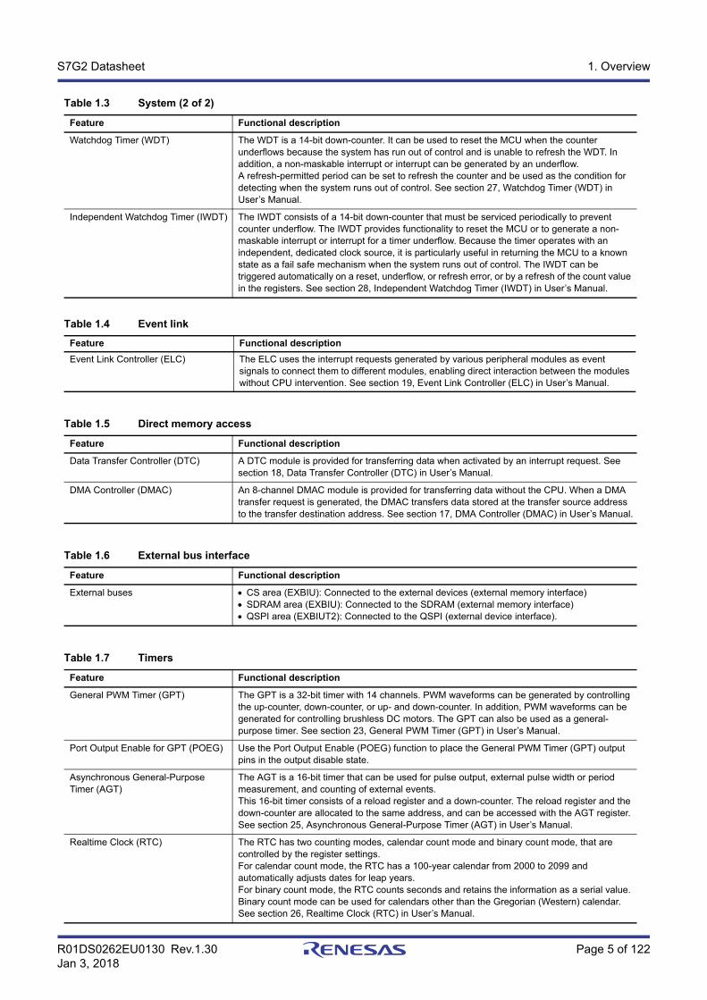
Watchdog Timer (WDT) The WDT is a 14-bit down-counter. It can be used to reset the MCU when the counter underflows because the system has run out of control and is unable to refresh the WDT. In addition, a non-maskable interrupt or interrupt can be generated by an underflow.A refresh-permitted period can be set to refresh the counter and be used as the condition for detecting when the system runs out of control. See section 27, Watchdog Timer (WDT) in User’s Manual.
Independent Watchdog Timer (IWDT) The IWDT consists of a 14-bit down-counter that must be serviced periodically to prevent counter underflow. The IWDT provides functionality to reset the MCU or to generate a non-maskable interrupt or interrupt for a timer underflow. Because the timer operates with an independent, dedicated clock source, it is particularly useful in returning the MCU to a known state as a fail safe mechanism when the system runs out of control. The IWDT can be triggered automatically on a reset, underflow, or refresh error, or by a refresh of the count value in the registers. See section 28, Independent Watchdog Timer (IWDT) in User’s Manual.
Table 1.4 Event link
Feature Functional description
Event Link Controller (ELC) The ELC uses the interrupt requests generated by various peripheral modules as event signals to connect them to different modules, enabling direct interaction between the modules without CPU intervention. See section 19, Event Link Controller (ELC) in User’s Manual.
Table 1.5 Direct memory access
Feature Functional description
Data Transfer Controller (DTC) A DTC module is provided for transferring data when activated by an interrupt request. See section 18, Data Transfer Controller (DTC) in User’s Manual.
DMA Controller (DMAC) An 8-channel DMAC module is provided for transferring data without the CPU. When a DMA transfer request is generated, the DMAC transfers data stored at the transfer source address to the transfer destination address. See section 17, DMA Controller (DMAC) in User’s Manual.
Table 1.6 External bus interface
Feature Functional description
External buses CS area (EXBIU): Connected to the external devices (external memory interface) SDRAM area (EXBIU): Connected to the SDRAM (external memory interface) QSPI area (EXBIUT2): Connected to the QSPI (external device interface).
Table 1.7 Timers
Feature Functional description
General PWM Timer (GPT) The GPT is a 32-bit timer with 14 channels. PWM waveforms can be generated by controlling the up-counter, down-counter, or up- and down-counter. In addition, PWM waveforms can be generated for controlling brushless DC motors. The GPT can also be used as a general-purpose timer. See section 23, General PWM Timer (GPT) in User’s Manual.
Port Output Enable for GPT (POEG) Use the Port Output Enable (POEG) function to place the General PWM Timer (GPT) output pins in the output disable state.
Asynchronous General-Purpose Timer (AGT)
The AGT is a 16-bit timer that can be used for pulse output, external pulse width or period measurement, and counting of external events.This 16-bit timer consists of a reload register and a down-counter. The reload register and the down-counter are allocated to the same address, and can be accessed with the AGT register. See section 25, Asynchronous General-Purpose Timer (AGT) in User’s Manual.
Realtime Clock (RTC) The RTC has two counting modes, calendar count mode and binary count mode, that are controlled by the register settings.For calendar count mode, the RTC has a 100-year calendar from 2000 to 2099 and automatically adjusts dates for leap years.For binary count mode, the RTC counts seconds and retains the information as a serial value. Binary count mode can be used for calendars other than the Gregorian (Western) calendar. See section 26, Realtime Clock (RTC) in User’s Manual.
Table 1.3 System (2 of 2)
Feature Functional description
R01DS0262EU0130 Rev.1.30 Page 6 of 122Jan 3, 2018
S7G2 Datasheet 1. Overview
Table 1.8 Communication interfaces (1 of 2)
Feature Functional description
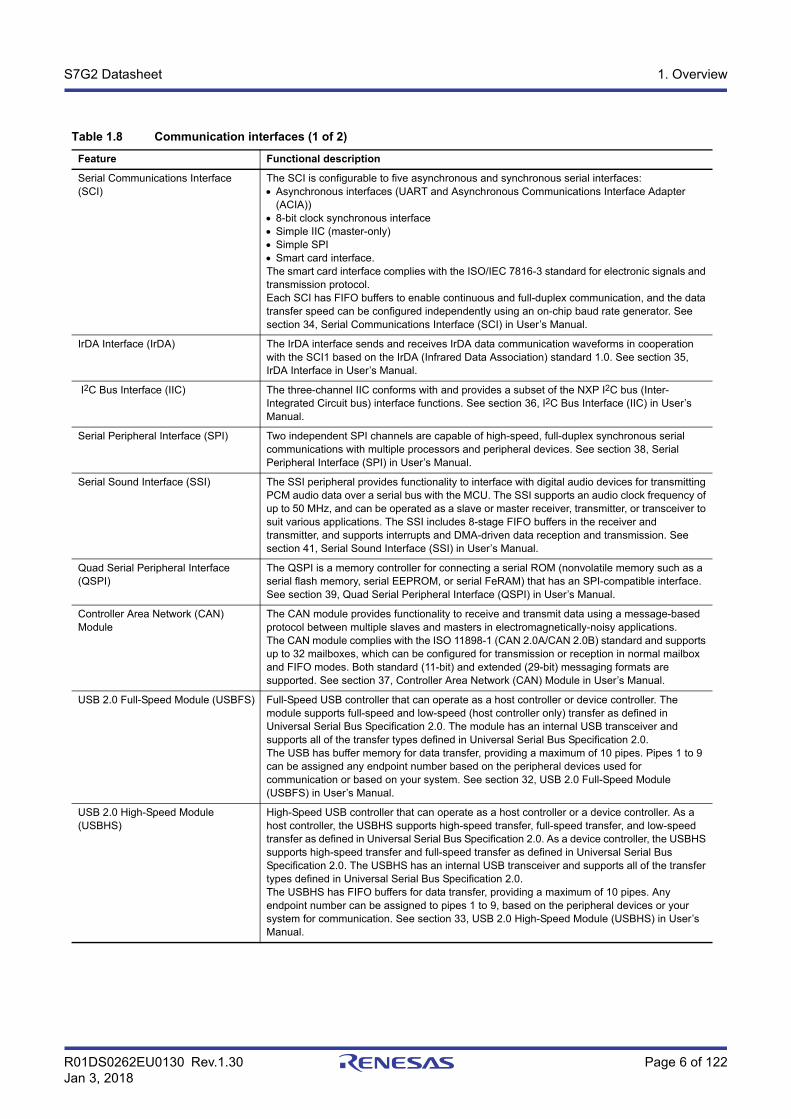
Serial Communications Interface (SCI)
The SCI is configurable to five asynchronous and synchronous serial interfaces: Asynchronous interfaces (UART and Asynchronous Communications Interface Adapter
(ACIA)) 8-bit clock synchronous interface Simple IIC (master-only) Simple SPI Smart card interface.The smart card interface complies with the ISO/IEC 7816-3 standard for electronic signals and transmission protocol.Each SCI has FIFO buffers to enable continuous and full-duplex communication, and the data transfer speed can be configured independently using an on-chip baud rate generator. See section 34, Serial Communications Interface (SCI) in User’s Manual.
IrDA Interface (IrDA) The IrDA interface sends and receives IrDA data communication waveforms in cooperation with the SCI1 based on the IrDA (Infrared Data Association) standard 1.0. See section 35, IrDA Interface in User’s Manual.
I2C Bus Interface (IIC) The three-channel IIC conforms with and provides a subset of the NXP I2C bus (Inter-Integrated Circuit bus) interface functions. See section 36, I2C Bus Interface (IIC) in User’s Manual.
Serial Peripheral Interface (SPI) Two independent SPI channels are capable of high-speed, full-duplex synchronous serial communications with multiple processors and peripheral devices. See section 38, Serial Peripheral Interface (SPI) in User’s Manual.
Serial Sound Interface (SSI) The SSI peripheral provides functionality to interface with digital audio devices for transmitting PCM audio data over a serial bus with the MCU. The SSI supports an audio clock frequency of up to 50 MHz, and can be operated as a slave or master receiver, transmitter, or transceiver to suit various applications. The SSI includes 8-stage FIFO buffers in the receiver and transmitter, and supports interrupts and DMA-driven data reception and transmission. See section 41, Serial Sound Interface (SSI) in User’s Manual.
Quad Serial Peripheral Interface (QSPI)
The QSPI is a memory controller for connecting a serial ROM (nonvolatile memory such as a serial flash memory, serial EEPROM, or serial FeRAM) that has an SPI-compatible interface. See section 39, Quad Serial Peripheral Interface (QSPI) in User’s Manual.
Controller Area Network (CAN) Module
The CAN module provides functionality to receive and transmit data using a message-based protocol between multiple slaves and masters in electromagnetically-noisy applications.The CAN module complies with the ISO 11898-1 (CAN 2.0A/CAN 2.0B) standard and supports up to 32 mailboxes, which can be configured for transmission or reception in normal mailbox and FIFO modes. Both standard (11-bit) and extended (29-bit) messaging formats are supported. See section 37, Controller Area Network (CAN) Module in User’s Manual.
USB 2.0 Full-Speed Module (USBFS) Full-Speed USB controller that can operate as a host controller or device controller. The module supports full-speed and low-speed (host controller only) transfer as defined in Universal Serial Bus Specification 2.0. The module has an internal USB transceiver and supports all of the transfer types defined in Universal Serial Bus Specification 2.0.The USB has buffer memory for data transfer, providing a maximum of 10 pipes. Pipes 1 to 9 can be assigned any endpoint number based on the peripheral devices used for communication or based on your system. See section 32, USB 2.0 Full-Speed Module (USBFS) in User’s Manual.
USB 2.0 High-Speed Module (USBHS)
High-Speed USB controller that can operate as a host controller or a device controller. As a host controller, the USBHS supports high-speed transfer, full-speed transfer, and low-speed transfer as defined in Universal Serial Bus Specification 2.0. As a device controller, the USBHS supports high-speed transfer and full-speed transfer as defined in Universal Serial Bus Specification 2.0. The USBHS has an internal USB transceiver and supports all of the transfer types defined in Universal Serial Bus Specification 2.0.The USBHS has FIFO buffers for data transfer, providing a maximum of 10 pipes. Any endpoint number can be assigned to pipes 1 to 9, based on the peripheral devices or your system for communication. See section 33, USB 2.0 High-Speed Module (USBHS) in User’s Manual.
R01DS0262EU0130 Rev.1.30 Page 7 of 122Jan 3, 2018
S7G2 Datasheet 1. Overview
Ethernet MAC with IEEE 1588 PTP (ETHERC)
Two-channel Ethernet MAC Controller (ETHERC) compliant with the Ethernet/IEEE802.3 Media Access Control (MAC) layer protocol. Each ETHERC channel provides one channel of the MAC layer interface, connecting the MCU to the physical layer LSI (PHY-LSI) that allows transmission and reception of frames compliant with the Ethernet and IEEE802.3 standards. The ETHERC is connected to the Ethernet DMA Controller (EDMAC) so data can be transferred without using the CPU.To handle timing and synchronization between devices, an on-chip Precision Time Protocol (PTP) module for the Ethernet PTP Controller (EPTPC) applies the PTP defined in the IEEE 1588-2008 version 2.0 standard.The EPTPC is composed of: Synchronization Frame Processing units (SYNFP0 and SYNFP1) A Packet Relation Controller unit (PRC-TC) A Statistical Time Correction Algorithm unit (STCA).Use the EPTPC in combination with the on-chip Ethernet MAC Controller (ETHERC) and the DMA Controller for the PTP Ethernet Controller (PTPEDMAC). See section 29, Ethernet MAC Controller (ETHERC) in User’s Manual.
SD/MMC Host Interface (SDHI) The SDHI and MultiMediaCard (MMC) interface module provides the functionality required to connect a variety of external memory cards to the MCU. The SDHI supports both 1- and 4-bit buses for connecting memory cards that support SD, SDHC, and SDXC formats. When developing host devices that are compliant with the SD Specifications, you must comply with the SD Host/Ancillary Product License Agreement (SD HALA).The MMC interface supports 1-, 4-, and 8-bit MMC buses that provide eMMC 4.51 (JEDEC Standard JESD 84-B451) device access. This interface also provides backward compatibility and supports high-speed SDR transfer modes. See section 43, SD/MMC Host Interface (SDHI) in User’s Manual.
Table 1.9 Analog
Feature Functional description
12-Bit A/D Converter (ADC12) Up to two successive approximation 12-Bit A/D Converters are provided. In unit 0, up to 13 analog input channels are selectable. In unit 1, up to 12 analog input channels, the temperature sensor output, and an internal reference voltage are selectable for conversion. The A/D conversion accuracy is selectable from 12-, 10-, and 8-bit conversion, making it possible to optimize the tradeoff between speed and resolution in generating a digital value. See section 46, 12-Bit A/D Converter (ADC12) in User’s Manual.
12-Bit D/A Converter (DAC12) The DAC12 D/A converts data and includes an output amplifier. See section 47, 12-Bit D/A Converter (DAC12) in User’s Manual.
Temperature sensor (TSN) The on-chip temperature sensor can determine and monitor the die temperature for reliable operation of the device. The sensor outputs a voltage directly proportional to the die temperature, and the relationship between the die temperature and the output voltage is linear.The output voltage is provided to the ADC12 for conversion and can also be used by the end application. See section 48, Temperature Sensor (TSN) in User’s Manual.
High-Speed Analog Comparator (ACMPHS)
Analog comparators can be used to compare a test voltage with a reference voltage and to provide a digital output based on the conversion result.Both the test and reference voltages can be provided to the comparator from internal sources such as the DAC12 output and internal reference voltage, and an external source with or without an internal PGA.Such flexibility is useful in applications that require go/no-go comparisons to be performed between analog signals without necessarily requiring A/D conversion. See section 49, High-Speed Analog Comparator (ACMPHS) in User’s Manual.
Table 1.10 Human machine interfaces
Feature Functional description
Capacitive Touch Sensing Unit (CTSU)
The CTSU measures the electrostatic capacitance of the touch sensor. Changes in the electrostatic capacitance are determined by the software, which enables the CTSU to detect whether a finger is in contact with the touch sensor. The electrode surface of the touch sensor is usually enclosed with an electrical insulator so that fingers do not come into direct contact with the electrodes. See section 50, Capacitive Touch Sensing Unit (CTSU) in User’s Manual.
Table 1.8 Communication interfaces (2 of 2)
Feature Functional description
R01DS0262EU0130 Rev.1.30 Page 8 of 122Jan 3, 2018
S7G2 Datasheet 1. Overview
Table 1.11 Graphics
Feature Functional description
Graphics LCD Controller (GLCDC) The GLCDC provides multiple functions and supports various data formats and panels. Key GLCDC features include: GPX bus master function for accessing graphics data Superimposition of three planes (single color background plane, graphic 1 plane, and
graphic 2 plane) Support for many types of 32- or 16-bit per pixel graphics data and 8-, 4-, or 1-bit LUT data
format Digital interface signal output supporting a video image size of WVGA or greater.See section 57, Graphics LCD Controller (GLCDC) in User’s Manual.
2D Drawing Engine (DRW) The 2D Drawing Engine (DRW) provides flexible functions that can support almost any object geometry rather than being bound to only a few specific geometries such as lines, triangles, or circles. The edges of every object can be independently blurred or antialiased.Rasterization is executed at one pixel per clock on the bounding box of the object from left to right and top to bottom. The DRW can also raster from bottom to top to optimize the performance in certain cases. In addition, optimization methods are available to avoid rasterization of many empty pixels of the bounding box.The distances to the edges of the object are calculated by a set of edge equations for every pixel of the bounding box. These edge equations can be combined to describe the entire object.If a pixel is inside the object, it is selected for rendering. If it is outside, it is discarded. If it is on the edge, an alpha value can be chosen proportional to the distance of the pixel to the nearest edge for antialiasing.Every pixel that is selected for rendering can be textured. The resulting aRGB quadruple can be modified by a general raster operation approach independently for each of the four channels. The aRGB quadruples can then be blended with one of the multiple blend modes of the DRW.The DRW provides two inputs (texture read and framebuffer read), and one output (framebuffer write).The internal color format is always aRGB (8888). The color formats from the inputs are converted to the internal format on read and a conversion back is made on write.See section 55, 2D Drawing Engine (DRW) in User’s Manual.
JPEG Codec (JPEG) The JPEG Codec (JPEG) incorporates a JPEG codec that conforms to the JPEG baseline compression and decompression standard. This provides high-speed compression of image data and high-speed decoding of JPEG data. See section 56, JPEG Codec in User’s Manual.
Parallel Data Capture Unit (PDC) One PDC unit is provided for communicating with external I/O devices, including image sensors, and transferring parallel data such as an image output from the external I/O device through the DTC or DMAC to the on-chip SRAM and external address spaces (the CS and SDRAM areas). See section 44, Parallel Data Capture Unit (PDC) in User’s Manual.
Table 1.12 Data processing
Feature Functional description
Cyclic Redundancy Check (CRC) calculator
The CRC calculator generates CRC codes to detect errors in the data. The bit order of CRC calculation results can be switched for LSB-first or MSB-first communication. Additionally, various CRC-generating polynomials are available. The snoop function allows monitoring reads from and writes to specific addresses. This function is useful in applications that require CRC code to be generated automatically in certain events, such as monitoring writes to the serial transmit buffer and reads from the serial receive buffer. See section 40, Cyclic Redundancy Check (CRC) Calculator in User’s Manual.
Data Operation Circuit (DOC) The DOC compares, adds, and subtracts 16-bit data. See section 51, Data Operation Circuit (DOC) in User’s Manual.
Sampling Rate Converter (SRC) The SRC converts the sampling rate of data produced by various audio decoders, such as the WMA, MP3, and AAC. Both 16-bit stereo and monaural data are supported. See section 42, Sampling Rate Converter (SRC) in User’s Manual.
R01DS0262EU0130 Rev.1.30 Page 9 of 122Jan 3, 2018
S7G2 Datasheet 1. Overview
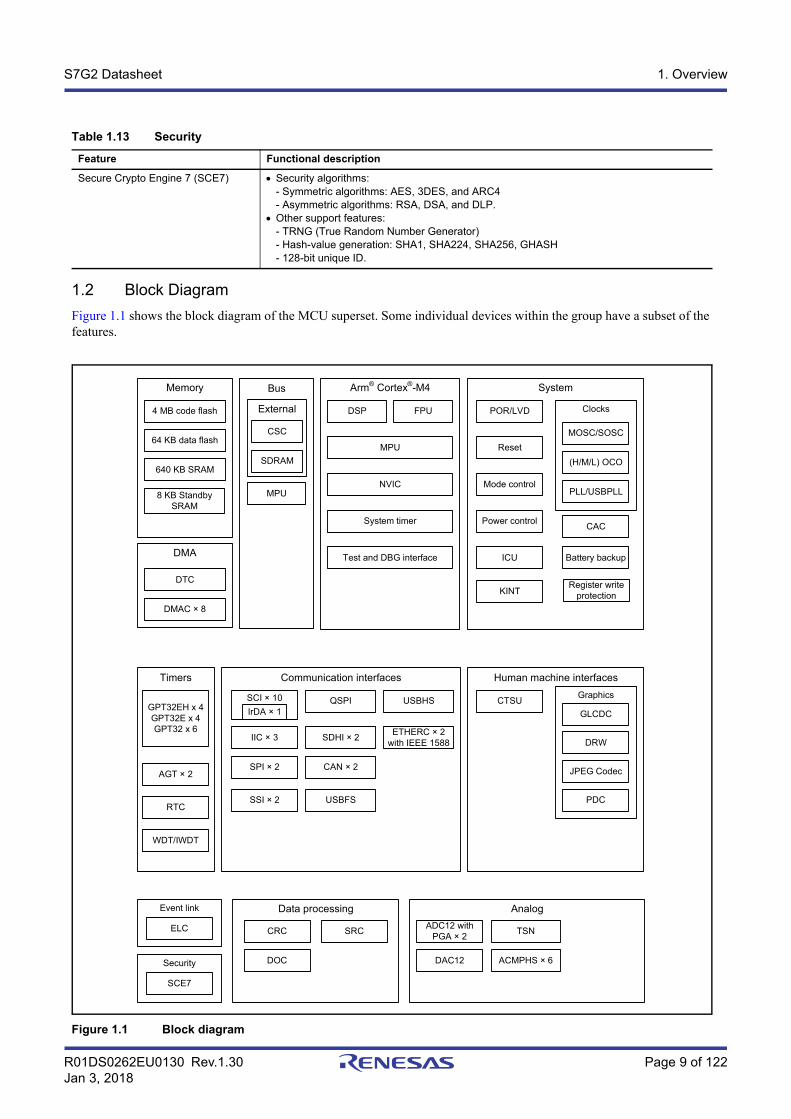
1.2 Block Diagram
Figure 1.1 shows the block diagram of the MCU superset. Some individual devices within the group have a subset of the features.
Figure 1.1 Block diagram
Table 1.13 Security
Feature Functional description
Secure Crypto Engine 7 (SCE7) Security algorithms:- Symmetric algorithms: AES, 3DES, and ARC4- Asymmetric algorithms: RSA, DSA, and DLP.
Other support features:- TRNG (True Random Number Generator)- Hash-value generation: SHA1, SHA224, SHA256, GHASH- 128-bit unique ID.
Memory
4 MB code flash
64 KB data flash
640 KB SRAM
DMA
DMAC × 8
System
Mode control
Power control
ICU
MOSC/SOSC
Clocks
(H/M/L) OCO
PLL/USBPLL
Battery backup
GPT32EH x 4GPT32E x 4GPT32 x 6
Timers
AGT × 2
RTC
CTSU
Arm® Cortex®-M4
DSP FPU
MPU
NVIC
System timer
Test and DBG interface
Bus
MPU
DTC
CSC
External
SDRAM
WDT/IWDT
CAC
POR/LVD
Reset
Human machine interfaces
GLCDC
Graphics
DRW
JPEG Codec
PDC
ELC
Event link
SCE7
Security
Analog
CRC
Data processing
DOC
SRC
Communication interfaces
QSPI USBHS
IIC × 3 SDHI × 2ETHERC × 2
with IEEE 1588
SPI × 2 CAN × 2
SSI × 2 USBFS
SCI × 10
IrDA × 1
TSN
DAC12 ACMPHS × 6
ADC12 with PGA × 2
8 KB Standby SRAM
Register write protectionKINT
R01DS0262EU0130 Rev.1.30 Page 10 of 122Jan 3, 2018
S7G2 Datasheet 1. Overview
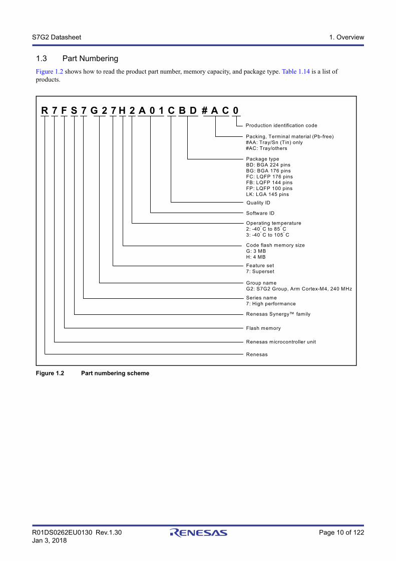
1.3 Part Numbering
Figure 1.2 shows how to read the product part number, memory capacity, and package type. Table 1.14 is a list of products.
Figure 1.2 Part numbering scheme
R 7 F S 7 G 2 7
Package typeBD: BGA 224 pinsBG: BGA 176 pinsFC: LQFP 176 pinsFB: LQFP 144 pinsFP: LQFP 100 pinsLK: LGA 145 pins
Quality ID
Software ID
Operating temperature2: -40° C to 85° C3: -40° C to 105° C
Code flash memory sizeG: 3 MBH: 4 MB
Feature set7: Superset
Group nameG2: S7G2 Group, Arm Cortex-M4, 240 MHz
Series name7: High performance
Renesas Synergy™ family
Flash memory
Renesas microcontroller unit
Renesas
H 2 A 0 1 C B D # A C 0
Packing, Terminal material (Pb-free)#AA: Tray/Sn (Tin) only#AC: Tray/others
Production identification code
R01DS0262EU0130 Rev.1.30 Page 11 of 122Jan 3, 2018
S7G2 Datasheet 1. Overview
1.4 Function Comparison
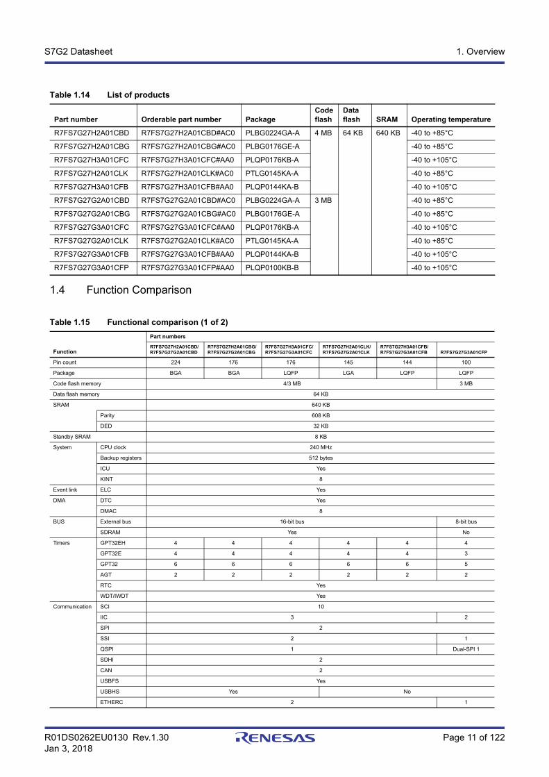
Table 1.14 List of products
Part number Orderable part number PackageCode flash
Data flash SRAM Operating temperature
R7FS7G27H2A01CBD R7FS7G27H2A01CBD#AC0 PLBG0224GA-A 4 MB 64 KB 640 KB -40 to +85°C
R7FS7G27H2A01CBG R7FS7G27H2A01CBG#AC0 PLBG0176GE-A -40 to +85°C
R7FS7G27H3A01CFC R7FS7G27H3A01CFC#AA0 PLQP0176KB-A -40 to +105°C
R7FS7G27H2A01CLK R7FS7G27H2A01CLK#AC0 PTLG0145KA-A -40 to +85°C
R7FS7G27H3A01CFB R7FS7G27H3A01CFB#AA0 PLQP0144KA-B -40 to +105°C
R7FS7G27G2A01CBD R7FS7G27G2A01CBD#AC0 PLBG0224GA-A 3 MB -40 to +85°C
R7FS7G27G2A01CBG R7FS7G27G2A01CBG#AC0 PLBG0176GE-A -40 to +85°C
R7FS7G27G3A01CFC R7FS7G27G3A01CFC#AA0 PLQP0176KB-A -40 to +105°C
R7FS7G27G2A01CLK R7FS7G27G2A01CLK#AC0 PTLG0145KA-A -40 to +85°C
R7FS7G27G3A01CFB R7FS7G27G3A01CFB#AA0 PLQP0144KA-B -40 to +105°C
R7FS7G27G3A01CFP R7FS7G27G3A01CFP#AA0 PLQP0100KB-B -40 to +105°C
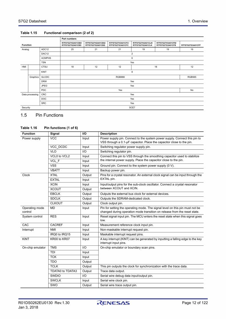
Table 1.15 Functional comparison (1 of 2)
Function
Part numbers
R7FS7G27H2A01CBD/R7FS7G27G2A01CBD
R7FS7G27H2A01CBG/R7FS7G27G2A01CBG
R7FS7G27H3A01CFC/R7FS7G27G3A01CFC
R7FS7G27H2A01CLK/R7FS7G27G2A01CLK
R7FS7G27H3A01CFB/R7FS7G27G3A01CFB R7FS7G27G3A01CFP
Pin count 224 176 176 145 144 100
Package BGA BGA LQFP LGA LQFP LQFP
Code flash memory 4/3 MB 3 MB
Data flash memory 64 KB
SRAM 640 KB
Parity 608 KB
DED 32 KB
Standby SRAM 8 KB
System CPU clock 240 MHz
Backup registers 512 bytes
ICU Yes
KINT 8
Event link ELC Yes
DMA DTC Yes
DMAC 8
BUS External bus 16-bit bus 8-bit bus
SDRAM Yes No
Timers GPT32EH 4 4 4 4 4 4
GPT32E 4 4 4 4 4 3
GPT32 6 6 6 6 6 5
AGT 2 2 2 2 2 2
RTC Yes
WDT/IWDT Yes
Communication SCI 10
IIC 3 2
SPI 2
SSI 2 1
QSPI 1 Dual-SPI 1
SDHI 2
CAN 2
USBFS Yes
USBHS Yes No
ETHERC 2 1
R01DS0262EU0130 Rev.1.30 Page 12 of 122Jan 3, 2018
S7G2 Datasheet 1. Overview
1.5 Pin Functions
Analog ADC12 25 21 21 19 19 16
DAC12 2
ACMPHS 6
TSN Yes
HMI CTSU 18 12 12 18 12
KINT 8
Graphics GLCDC RGB888 RGB565
DRW Yes
JPEG Yes
PDC Yes No
Data processing CRC Yes
DOC Yes
SRC Yes
Security SCE7
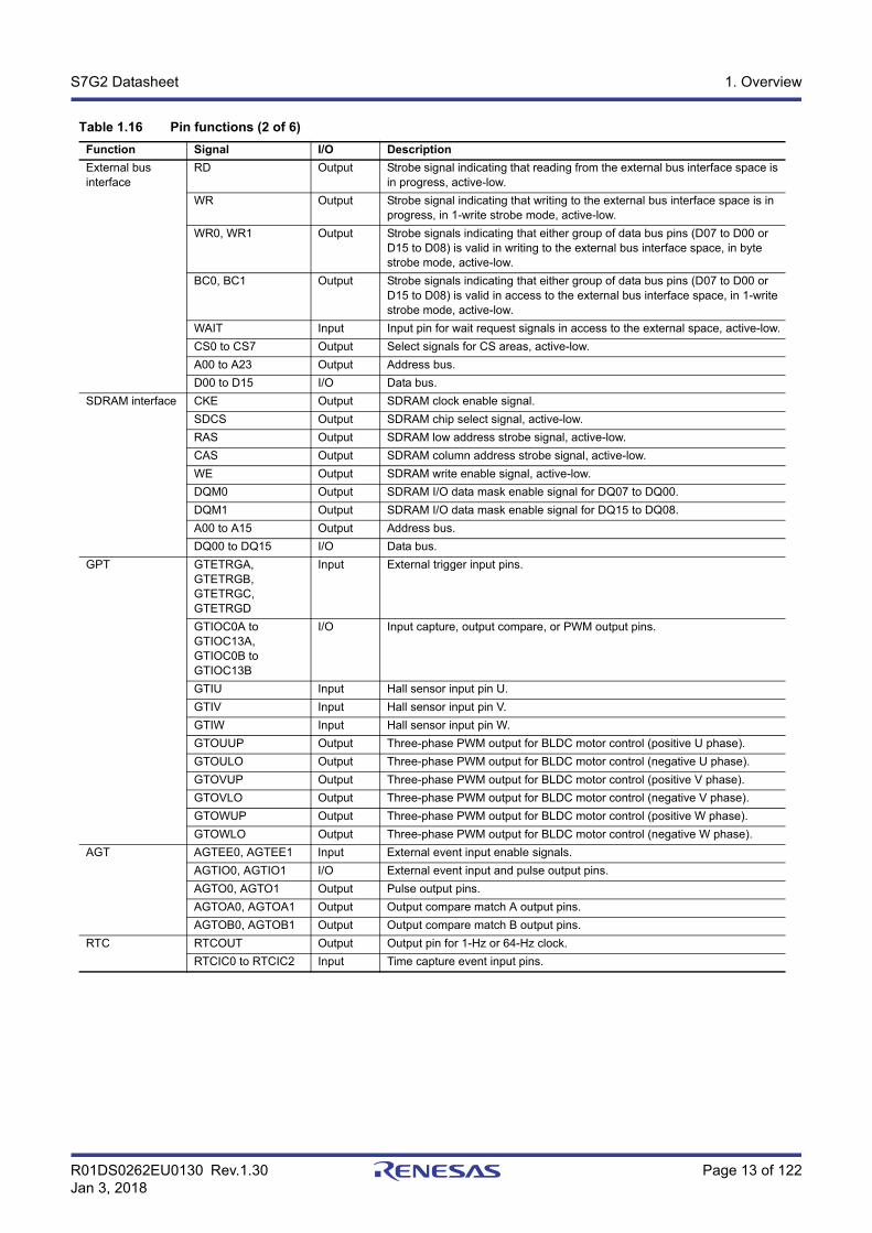
Table 1.16 Pin functions (1 of 6)
Function Signal I/O Description
Power supply VCC Input Power supply pin. Connect to the system power supply. Connect this pin to VSS through a 0.1-μF capacitor. Place the capacitor close to the pin.
VCC_DCDC Input Switching regulator power supply pin.
VLO I/O Switching regulator pin.
VCL0 to VCL2 Input Connect this pin to VSS through the smoothing capacitor used to stabilize the internal power supply. Place the capacitor close to the pin.VCL_F Input
VSS Input Ground pin. Connect to the system power supply (0 V).
VBATT Input Backup power pin.
Clock XTAL Output Pins for a crystal resonator. An external clock signal can be input through the EXTAL pin.EXTAL Input
XCIN Input Input/output pins for the sub-clock oscillator. Connect a crystal resonator between XCOUT and XCIN.XCOUT Output
EBCLK Output Outputs the external bus clock for external devices.
SDCLK Output Outputs the SDRAM-dedicated clock.
CLKOUT Output Clock output pin.
Operating mode control
MD Input Pin for setting the operating mode. The signal level on this pin must not be changed during operation mode transition on release from the reset state.
System control RES Input Reset signal input pin. The MCU enters the reset state when this signal goes low.
CAC CACREF Input Measurement reference clock input pin.
Interrupt NMI Input Non-maskable interrupt request pin.
IRQ0 to IRQ15 Input Maskable interrupt request pins.
KINT KR00 to KR07 Input A key interrupt (KINT) can be generated by inputting a falling edge to the key interrupt input pins.
On-chip emulator TMS I/O On-chip emulator or boundary scan pins.
TDI Input
TCK Input
TDO Output
TCLK Output This pin outputs the clock for synchronization with the trace data.
TDATA0 to TDATA3 Output Trace data output.
SWDIO I/O Serial wire debug data input/output pin.
SWCLK Input Serial wire clock pin.
SWO Output Serial wire trace output pin.
Table 1.15 Functional comparison (2 of 2)
Function
Part numbers
R7FS7G27H2A01CBD/R7FS7G27G2A01CBD
R7FS7G27H2A01CBG/R7FS7G27G2A01CBG
R7FS7G27H3A01CFC/R7FS7G27G3A01CFC
R7FS7G27H2A01CLK/R7FS7G27G2A01CLK
R7FS7G27H3A01CFB/R7FS7G27G3A01CFB R7FS7G27G3A01CFP
R01DS0262EU0130 Rev.1.30 Page 13 of 122Jan 3, 2018
S7G2 Datasheet 1. Overview
External bus interface
RD Output Strobe signal indicating that reading from the external bus interface space is in progress, active-low.
WR Output Strobe signal indicating that writing to the external bus interface space is in progress, in 1-write strobe mode, active-low.
WR0, WR1 Output Strobe signals indicating that either group of data bus pins (D07 to D00 or D15 to D08) is valid in writing to the external bus interface space, in byte strobe mode, active-low.
BC0, BC1 Output Strobe signals indicating that either group of data bus pins (D07 to D00 or D15 to D08) is valid in access to the external bus interface space, in 1-write strobe mode, active-low.
WAIT Input Input pin for wait request signals in access to the external space, active-low.
CS0 to CS7 Output Select signals for CS areas, active-low.
A00 to A23 Output Address bus.
D00 to D15 I/O Data bus.
SDRAM interface CKE Output SDRAM clock enable signal.
SDCS Output SDRAM chip select signal, active-low.
RAS Output SDRAM low address strobe signal, active-low.
CAS Output SDRAM column address strobe signal, active-low.
WE Output SDRAM write enable signal, active-low.
DQM0 Output SDRAM I/O data mask enable signal for DQ07 to DQ00.
DQM1 Output SDRAM I/O data mask enable signal for DQ15 to DQ08.
A00 to A15 Output Address bus.
DQ00 to DQ15 I/O Data bus.
GPT GTETRGA, GTETRGB, GTETRGC, GTETRGD
Input External trigger input pins.
GTIOC0A to GTIOC13A, GTIOC0B to GTIOC13B
I/O Input capture, output compare, or PWM output pins.
GTIU Input Hall sensor input pin U.
GTIV Input Hall sensor input pin V.
GTIW Input Hall sensor input pin W.
GTOUUP Output Three-phase PWM output for BLDC motor control (positive U phase).
GTOULO Output Three-phase PWM output for BLDC motor control (negative U phase).
GTOVUP Output Three-phase PWM output for BLDC motor control (positive V phase).
GTOVLO Output Three-phase PWM output for BLDC motor control (negative V phase).
GTOWUP Output Three-phase PWM output for BLDC motor control (positive W phase).
GTOWLO Output Three-phase PWM output for BLDC motor control (negative W phase).
AGT AGTEE0, AGTEE1 Input External event input enable signals.
AGTIO0, AGTIO1 I/O External event input and pulse output pins.
AGTO0, AGTO1 Output Pulse output pins.
AGTOA0, AGTOA1 Output Output compare match A output pins.
AGTOB0, AGTOB1 Output Output compare match B output pins.
RTC RTCOUT Output Output pin for 1-Hz or 64-Hz clock.
RTCIC0 to RTCIC2 Input Time capture event input pins.
Table 1.16 Pin functions (2 of 6)
Function Signal I/O Description
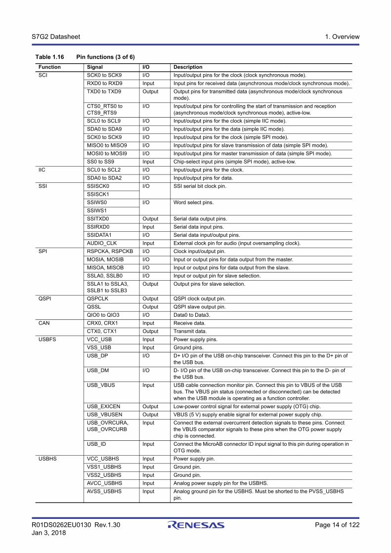
R01DS0262EU0130 Rev.1.30 Page 14 of 122Jan 3, 2018
S7G2 Datasheet 1. Overview
SCI SCK0 to SCK9 I/O Input/output pins for the clock (clock synchronous mode).
RXD0 to RXD9 Input Input pins for received data (asynchronous mode/clock synchronous mode).
TXD0 to TXD9 Output Output pins for transmitted data (asynchronous mode/clock synchronous mode).
CTS0_RTS0 to CTS9_RTS9
I/O Input/output pins for controlling the start of transmission and reception (asynchronous mode/clock synchronous mode), active-low.
SCL0 to SCL9 I/O Input/output pins for the clock (simple IIC mode).
SDA0 to SDA9 I/O Input/output pins for the data (simple IIC mode).
SCK0 to SCK9 I/O Input/output pins for the clock (simple SPI mode).
MISO0 to MISO9 I/O Input/output pins for slave transmission of data (simple SPI mode).
MOSI0 to MOSI9 I/O Input/output pins for master transmission of data (simple SPI mode).
SS0 to SS9 Input Chip-select input pins (simple SPI mode), active-low.
IIC SCL0 to SCL2 I/O Input/output pins for the clock.
SDA0 to SDA2 I/O Input/output pins for data.
SSI SSISCK0 I/O SSI serial bit clock pin.
SSISCK1
SSIWS0 I/O Word select pins.
SSIWS1
SSITXD0 Output Serial data output pins.
SSIRXD0 Input Serial data input pins.
SSIDATA1 I/O Serial data input/output pins.
AUDIO_CLK Input External clock pin for audio (input oversampling clock).
SPI RSPCKA, RSPCKB I/O Clock input/output pin.
MOSIA, MOSIB I/O Input or output pins for data output from the master.
MISOA, MISOB I/O Input or output pins for data output from the slave.
SSLA0, SSLB0 I/O Input or output pin for slave selection.
SSLA1 to SSLA3, SSLB1 to SSLB3
Output Output pins for slave selection.
QSPI QSPCLK Output QSPI clock output pin.
QSSL Output QSPI slave output pin.
QIO0 to QIO3 I/O Data0 to Data3.
CAN CRX0, CRX1 Input Receive data.
CTX0, CTX1 Output Transmit data.
USBFS VCC_USB Input Power supply pins.
VSS_USB Input Ground pins.
USB_DP I/O D+ I/O pin of the USB on-chip transceiver. Connect this pin to the D+ pin of the USB bus.
USB_DM I/O D- I/O pin of the USB on-chip transceiver. Connect this pin to the D- pin of the USB bus.
USB_VBUS Input USB cable connection monitor pin. Connect this pin to VBUS of the USB bus. The VBUS pin status (connected or disconnected) can be detected when the USB module is operating as a function controller.
USB_EXICEN Output Low-power control signal for external power supply (OTG) chip.
USB_VBUSEN Output VBUS (5 V) supply enable signal for external power supply chip.
USB_OVRCURA, USB_OVRCURB
Input Connect the external overcurrent detection signals to these pins. Connect the VBUS comparator signals to these pins when the OTG power supply chip is connected.
USB_ID Input Connect the MicroAB connector ID input signal to this pin during operation in OTG mode.
USBHS VCC_USBHS Input Power supply pin.
VSS1_USBHS Input Ground pin.
VSS2_USBHS Input Ground pin.
AVCC_USBHS Input Analog power supply pin for the USBHS.
AVSS_USBHS Input Analog ground pin for the USBHS. Must be shorted to the PVSS_USBHS pin.
Table 1.16 Pin functions (3 of 6)
Function Signal I/O Description
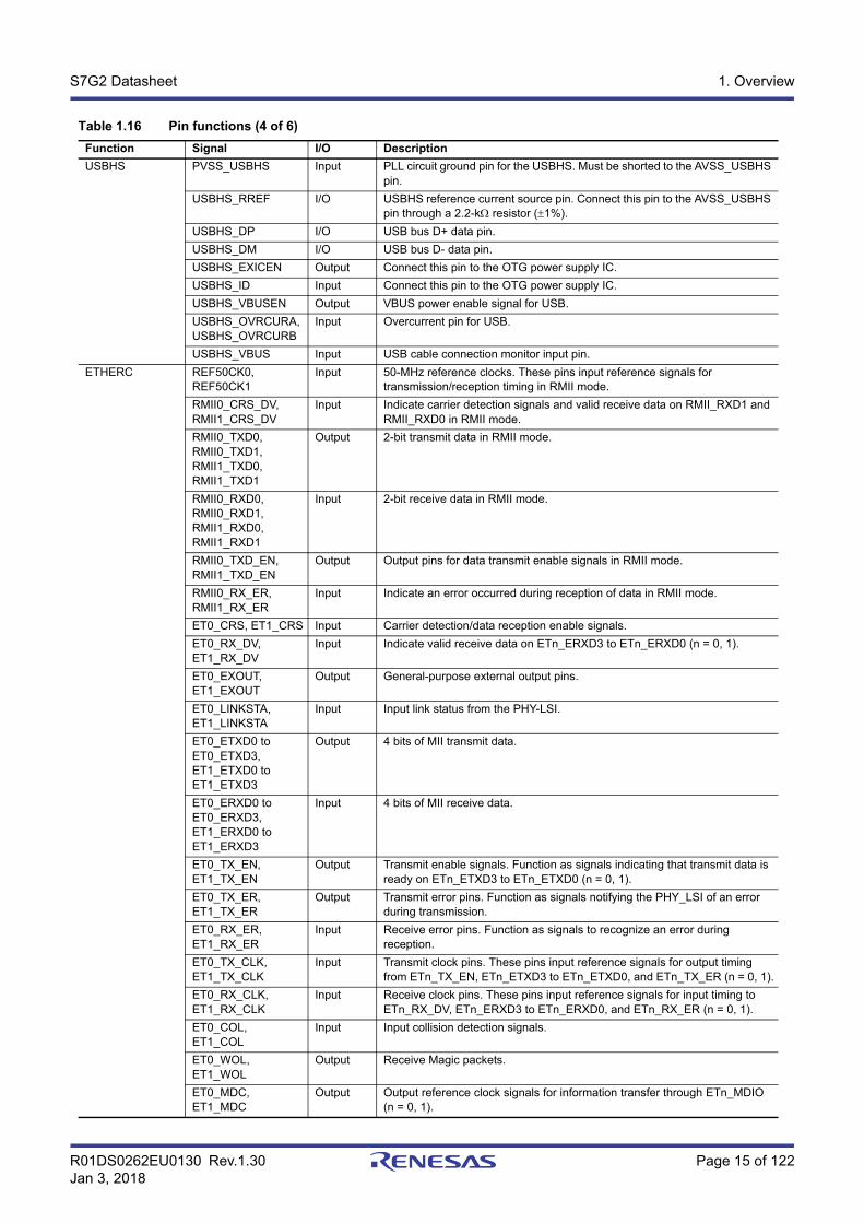
R01DS0262EU0130 Rev.1.30 Page 15 of 122Jan 3, 2018
S7G2 Datasheet 1. Overview
USBHS PVSS_USBHS Input PLL circuit ground pin for the USBHS. Must be shorted to the AVSS_USBHS pin.
USBHS_RREF I/O USBHS reference current source pin. Connect this pin to the AVSS_USBHS pin through a 2.2-k resistor (1%).
USBHS_DP I/O USB bus D+ data pin.
USBHS_DM I/O USB bus D- data pin.
USBHS_EXICEN Output Connect this pin to the OTG power supply IC.
USBHS_ID Input Connect this pin to the OTG power supply IC.
USBHS_VBUSEN Output VBUS power enable signal for USB.
USBHS_OVRCURA, USBHS_OVRCURB
Input Overcurrent pin for USB.
USBHS_VBUS Input USB cable connection monitor input pin.
ETHERC REF50CK0, REF50CK1
Input 50-MHz reference clocks. These pins input reference signals for transmission/reception timing in RMII mode.
RMII0_CRS_DV, RMII1_CRS_DV
Input Indicate carrier detection signals and valid receive data on RMII_RXD1 and RMII_RXD0 in RMII mode.
RMII0_TXD0, RMII0_TXD1,RMII1_TXD0, RMII1_TXD1
Output 2-bit transmit data in RMII mode.
RMII0_RXD0, RMII0_RXD1, RMII1_RXD0, RMII1_RXD1
Input 2-bit receive data in RMII mode.
RMII0_TXD_EN, RMII1_TXD_EN
Output Output pins for data transmit enable signals in RMII mode.
RMII0_RX_ER, RMII1_RX_ER
Input Indicate an error occurred during reception of data in RMII mode.
ET0_CRS, ET1_CRS Input Carrier detection/data reception enable signals.
ET0_RX_DV, ET1_RX_DV
Input Indicate valid receive data on ETn_ERXD3 to ETn_ERXD0 (n = 0, 1).
ET0_EXOUT, ET1_EXOUT
Output General-purpose external output pins.
ET0_LINKSTA, ET1_LINKSTA
Input Input link status from the PHY-LSI.
ET0_ETXD0 to ET0_ETXD3, ET1_ETXD0 to ET1_ETXD3
Output 4 bits of MII transmit data.
ET0_ERXD0 to ET0_ERXD3, ET1_ERXD0 to ET1_ERXD3
Input 4 bits of MII receive data.
ET0_TX_EN, ET1_TX_EN
Output Transmit enable signals. Function as signals indicating that transmit data is ready on ETn_ETXD3 to ETn_ETXD0 (n = 0, 1).
ET0_TX_ER, ET1_TX_ER
Output Transmit error pins. Function as signals notifying the PHY_LSI of an error during transmission.
ET0_RX_ER, ET1_RX_ER
Input Receive error pins. Function as signals to recognize an error during reception.
ET0_TX_CLK, ET1_TX_CLK
Input Transmit clock pins. These pins input reference signals for output timing from ETn_TX_EN, ETn_ETXD3 to ETn_ETXD0, and ETn_TX_ER (n = 0, 1).
ET0_RX_CLK, ET1_RX_CLK
Input Receive clock pins. These pins input reference signals for input timing to ETn_RX_DV, ETn_ERXD3 to ETn_ERXD0, and ETn_RX_ER (n = 0, 1).
ET0_COL, ET1_COL
Input Input collision detection signals.
ET0_WOL, ET1_WOL
Output Receive Magic packets.
ET0_MDC, ET1_MDC
Output Output reference clock signals for information transfer through ETn_MDIO (n = 0, 1).
Table 1.16 Pin functions (4 of 6)
Function Signal I/O Description
R01DS0262EU0130 Rev.1.30 Page 16 of 122Jan 3, 2018
S7G2 Datasheet 1. Overview
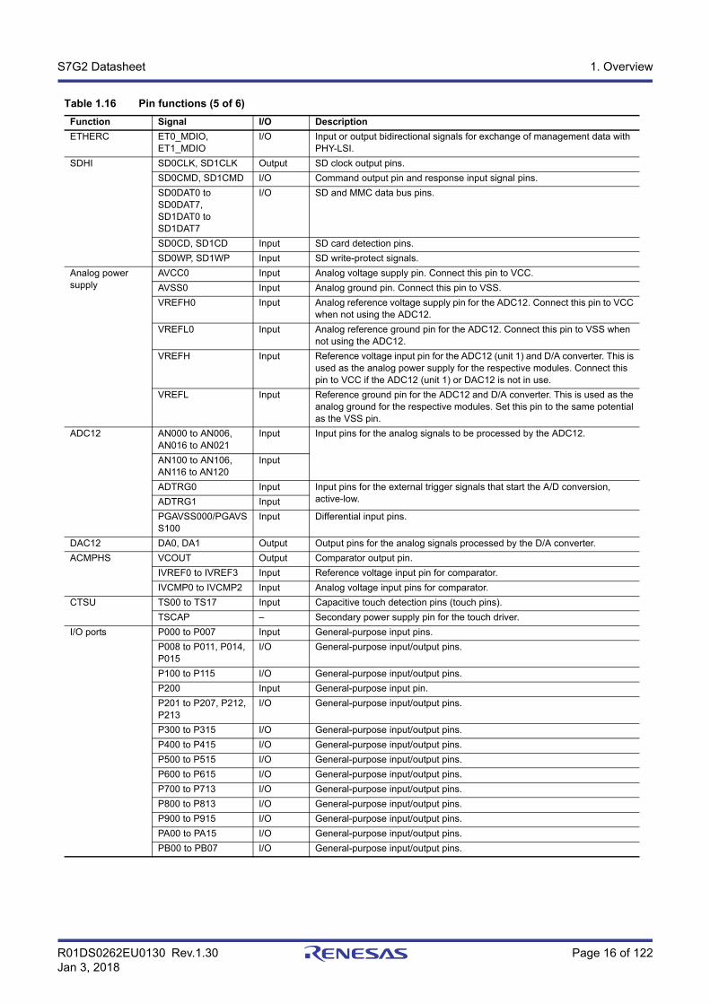
ETHERC ET0_MDIO, ET1_MDIO
I/O Input or output bidirectional signals for exchange of management data with PHY-LSI.
SDHI SD0CLK, SD1CLK Output SD clock output pins.
SD0CMD, SD1CMD I/O Command output pin and response input signal pins.
SD0DAT0 to SD0DAT7,SD1DAT0 to SD1DAT7
I/O SD and MMC data bus pins.
SD0CD, SD1CD Input SD card detection pins.
SD0WP, SD1WP Input SD write-protect signals.
Analog power supply
AVCC0 Input Analog voltage supply pin. Connect this pin to VCC.
AVSS0 Input Analog ground pin. Connect this pin to VSS.
VREFH0 Input Analog reference voltage supply pin for the ADC12. Connect this pin to VCC when not using the ADC12.
VREFL0 Input Analog reference ground pin for the ADC12. Connect this pin to VSS when not using the ADC12.
VREFH Input Reference voltage input pin for the ADC12 (unit 1) and D/A converter. This is used as the analog power supply for the respective modules. Connect this pin to VCC if the ADC12 (unit 1) or DAC12 is not in use.
VREFL Input Reference ground pin for the ADC12 and D/A converter. This is used as the analog ground for the respective modules. Set this pin to the same potential as the VSS pin.
ADC12 AN000 to AN006, AN016 to AN021
Input Input pins for the analog signals to be processed by the ADC12.
AN100 to AN106, AN116 to AN120
Input
ADTRG0 Input Input pins for the external trigger signals that start the A/D conversion, active-low.ADTRG1 Input
PGAVSS000/PGAVSS100
Input Differential input pins.
DAC12 DA0, DA1 Output Output pins for the analog signals processed by the D/A converter.
ACMPHS VCOUT Output Comparator output pin.
IVREF0 to IVREF3 Input Reference voltage input pin for comparator.
IVCMP0 to IVCMP2 Input Analog voltage input pins for comparator.
CTSU TS00 to TS17 Input Capacitive touch detection pins (touch pins).
TSCAP – Secondary power supply pin for the touch driver.
I/O ports P000 to P007 Input General-purpose input pins.
P008 to P011, P014, P015
I/O General-purpose input/output pins.
P100 to P115 I/O General-purpose input/output pins.
P200 Input General-purpose input pin.
P201 to P207, P212, P213
I/O General-purpose input/output pins.
P300 to P315 I/O General-purpose input/output pins.
P400 to P415 I/O General-purpose input/output pins.
P500 to P515 I/O General-purpose input/output pins.
P600 to P615 I/O General-purpose input/output pins.
P700 to P713 I/O General-purpose input/output pins.
P800 to P813 I/O General-purpose input/output pins.
P900 to P915 I/O General-purpose input/output pins.
PA00 to PA15 I/O General-purpose input/output pins.
PB00 to PB07 I/O General-purpose input/output pins.
Table 1.16 Pin functions (5 of 6)
Function Signal I/O Description
R01DS0262EU0130 Rev.1.30 Page 17 of 122Jan 3, 2018
S7G2 Datasheet 1. Overview
1.6 Pin Assignments
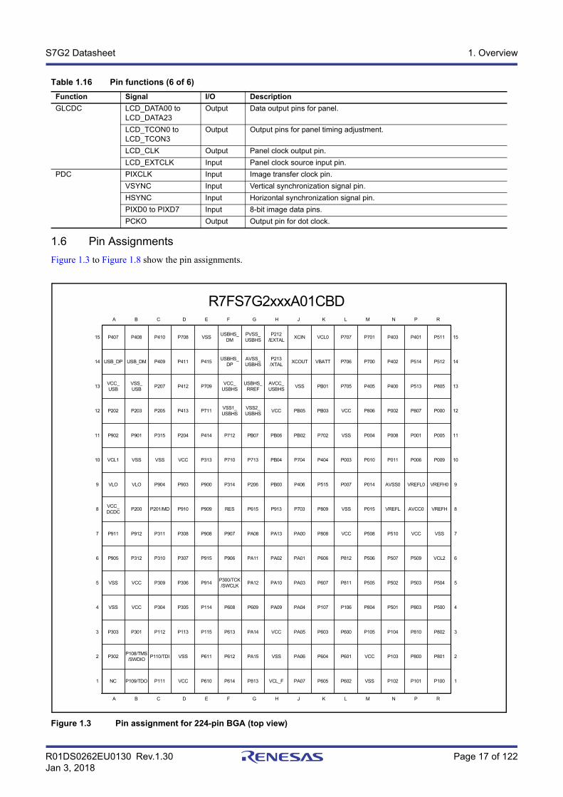
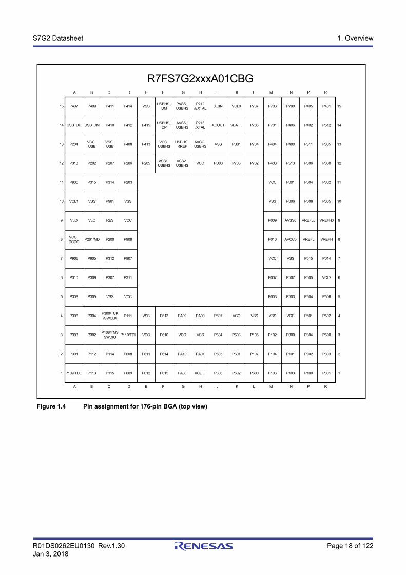
Figure 1.3 to Figure 1.8 show the pin assignments.
Figure 1.3 Pin assignment for 224-pin BGA (top view)
GLCDC LCD_DATA00 to LCD_DATA23
Output Data output pins for panel.
LCD_TCON0 toLCD_TCON3
Output Output pins for panel timing adjustment.
LCD_CLK Output Panel clock output pin.
LCD_EXTCLK Input Panel clock source input pin.
PDC PIXCLK Input Image transfer clock pin.
VSYNC Input Vertical synchronization signal pin.
HSYNC Input Horizontal synchronization signal pin.
PIXD0 to PIXD7 Input 8-bit image data pins.
PCKO Output Output pin for dot clock.
Table 1.16 Pin functions (6 of 6)
Function Signal I/O Description
N P RK L MG H JD E FA B C
N P RK L MG H JD E FA B C
P511
P512
P805
P000
P005
P009
VREFH0
VREFH
VSS
VCL2
P504
P500
P802
P801
P100
P401
P514
P513
P807
P001
P006
VREFL0
AVCC0
VCC
P509
P503
P803
P810
P800
P101
P403
P402
P400
P002
P008
P011
AVSS0
VREFL
P510
P507
P502
P501
P104
P103
P102
P701
P700
P405
P806
P004
P010
P014
P015
P508
P506
P505
P804
P105
VCC
VSS
P707
P706
P705
VCC
VSS
P003
P007
VSS
VCC
P812
P811
P106
P600
P601
P602
VCL0
VBATT
PB01
PB03
P702
P404
P515
P809
P808
P606
P607
P107
P603
P604
P605
XCIN
XCOUT
VSS
PB05
PB02
P704
P406
P703
PA00
PA01
PA03
PA04
PA05
PA06
PA07
P212/EXTAL
P213/XTAL
AVCC_USBHS
VCC
PB06
PB04
PB00
P913
PA13
PA02
PA10
PA09
VCC
VSS
VCL_F
PVSS_USBHS
AVSS_USBHS
USBHS_RREF
VSS2_USBHS
PB07
P713
P206
P615
PA08
PA11
PA12
P609
PA14
PA15
P813
USBHS_DM
USBHS_DP
VCC_USBHS
VSS1_USBHS
P712
P710
P314
RES
P907
P906
P300/TCK/SWCLK
P608
P613
P612
P614
VSS
P415
P709
P711
P414
P313
P900
P909
P908
P915
P914
P114
P115
P611
P610
P708
P411
P412
P413
P204
VCC
P903
P910
P308
P307
P306
P305
P113
VSS
VCC
P410
P409
P207
P205
P315
VSS
P904
P201/MD
P311
P310
P309
P304
P112
P110/TDI
P111
P408
USB_DM
VSS_USB
P203
P901
VSS
VLO
P200
P912
P312
VCC
VCC
P301
P108/TMS/SWDIO
P109/TDO
P407
USB_DP
VCC_USB
P202
P902
VCL1
VLO
VCC_DCDC
P911
P905
VSS
VSS
P303
P302
NC
15
14
13
12
11
10
9
8
7
6
5
4
3
2
1
15
14
13
12
11
10
9
8
7
6
5
4
3
2
1
R7FS7G2xxxA01CBD
R01DS0262EU0130 Rev.1.30 Page 18 of 122Jan 3, 2018
S7G2 Datasheet 1. Overview
Figure 1.4 Pin assignment for 176-pin BGA (top view)
P201/MD
N P RK L MG H JD E FA B C
N P RK L MG H JD E FA B C
P401
P512
P805
P000
P002
P005
VREFH0
VREFH
P014
VCL2
P506
P502
P500
P803
P801
P405
P402
P511
P806
P004
P008
VREFL0
VREFL
P015
P505
P504
P501
P804
P802
P100
P700
P406
P400
P513
P001
P006
AVSS0
AVCC0
VSS
P507
P503
VCC
P800
P101
P103
P703
P701
P404
P403
VCC
VSS
P009
P010
VCC
P007
P003
VSS
P102
P104
P106
P707
P706
P704
P702
VSS
P105
P107
P600
VCL0
VBATT
PB01
P705
VCC
P603
P601
P602
XCIN
XCOUT
VSS
PB00
P607
P604
P605
P606
P212/EXTAL
P213/XTAL
AVCC_USBHS
VCC
PA00
VSS
PA01
VCL_F
PVSS_USBHS
AVSS_USBHS
USBHS_RREF
VSS2_USBHS
PA09
VCC
PA10
PA08
USBHS_DM
USBHS_DP
VCC_USBHS
VSS1_USBHS
P613
P610
P614
P615
VSS
P415
P413
P205
VSS
VCC
P611
P612
P414
P412
P408
P206
P203
VSS
VCC
P908
P907
P311
VCC
P111
P110/TDI
P608
P609
P411
P410
VSS_USB
P207
P314
P901
RES
P200
P312
P307
VSS
P300/TCK/SWCLK
P108/TMSSWDIO
P114
P115
P409
USB_DM
VCC_USB
P202
P315
VSS
VLO
P905
P309
P305
P304
P302
P112
P113
P407
USB_DP
P204
P313
P900
VCL1
VLO
VCC_DCDC
P906
P310
P308
P306
P303
P301
P109/TDO
15
14
13
12
11
10
9
8
7
6
5
4
3
2
1
15
14
13
12
11
10
9
8
7
6
5
4
3
2
1
R7FS7G2xxxA01CBG
R01DS0262EU0130 Rev.1.30 Page 19 of 122Jan 3, 2018
S7G2 Datasheet 1. Overview
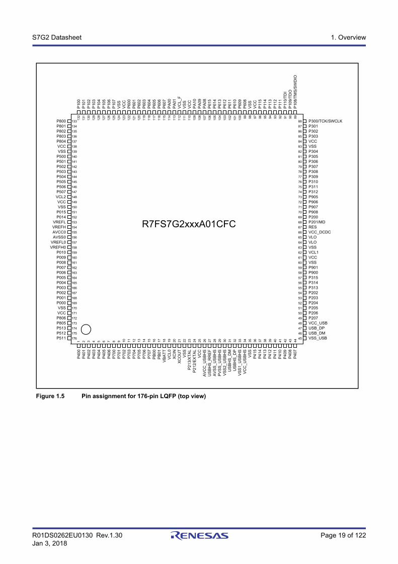
Figure 1.5 Pin assignment for 176-pin LQFP (top view)
1 2 3 4 5 6 7 8 9 10 11 12 13 14 15 16 17 18 19 20 21 22 23 24 25 26 27 28 29 30 31 32 33 34 35 36 37 38 39 40 41 42 43 44
132
131
130
129
128
127
126
125
124
123
122
121
120
119
118
117
116
115
114
113
112
111
110
109
108
107
106
105
104
103
102
101
100 99 98 97 96 95 94 93 92 91 90 89
88
87
86
85
84
83
82
81
80
79
78
77
76
75
74
73
72
71
70
69
68
67
66
65
64
63
62
61
60
59
58
57
56
55
54
53
52
51
50
49
48
47
46
45
133
134
135
136
137
138
139
140
141
142
143
144
145
146
147
148
149
150
151
152
153
154
155
156
157
158
159
160
161
162
163
164
165
166
167
168
169
170
171
172
173
174
175
176
P802P803P804VCCVSS
P500P501P502P503P504P505P506
VCL2VCCVSS
P015P014
VREFLVREFHAVCC0AVSS0
VREFL0VREFH0
P010
P008
P006
P004
P002
P000
VCC
P805
P511
P801
P507
P512VSS_USB
P10
0
P10
2P
103
P10
4P
105
P10
6P
107
VS
SV
CC
P60
0P
601
P60
2P
603
P60
5P
606
P60
7P
A00
PA
01V
CL_
FV
SS
VC
CP
A10
PA
09P
A08
P61
5
P61
3P
612
P60
9P
608
VC
C
P11
4
P11
2
P10
8/T
MS
/SW
DIO
P10
1
P60
4
P10
9/T
DO
P4
00
P4
02
P4
03
P4
04
P4
05
P4
06
P7
00
P7
01
P7
02
P7
03
P7
04
P7
05
P7
06
PB
00
PB
01
VB
AT
TV
CL
0X
CIN
XC
OU
TV
SS
P2
13/
XT
AL
VC
C
US
BH
S_R
RE
F
US
BH
S_
DM
VS
S1_
US
BH
S
VS
S
P4
14
P4
12
P4
10P
40
9
P4
07
P2
12/E
XT
AL
P4
01
P7
07
PV
SS
_U
SB
HS
P800
AV
CC
_U
SB
HS
AV
SS
_U
SB
HS
VS
S2_
US
BH
S
US
BH
S_
DP
VC
C_
US
BH
S
P4
15
P4
13
P4
11
P4
08
USB_DMUSB_DPVCC_USBP207P206P205P204P203P202P313P314P315P900P901VSSVCCVCL1
VLOVLO
P312
P310P309P308P307P306P305P304VSSVCC
VSS
VCC_DCDCRESP201/MDP200P908P907P906P905
P311
P303P302P301P300/TCK/SWCLK
P61
4
P61
1P
610
VS
S
P11
5
P11
3
P11
0/T
DI
P11
1
P009
P007
P005
P003
P001
VSS
P513
P806
R7FS7G2xxxA01CFC
R01DS0262EU0130 Rev.1.30 Page 20 of 122Jan 3, 2018
S7G2 Datasheet 1. Overview
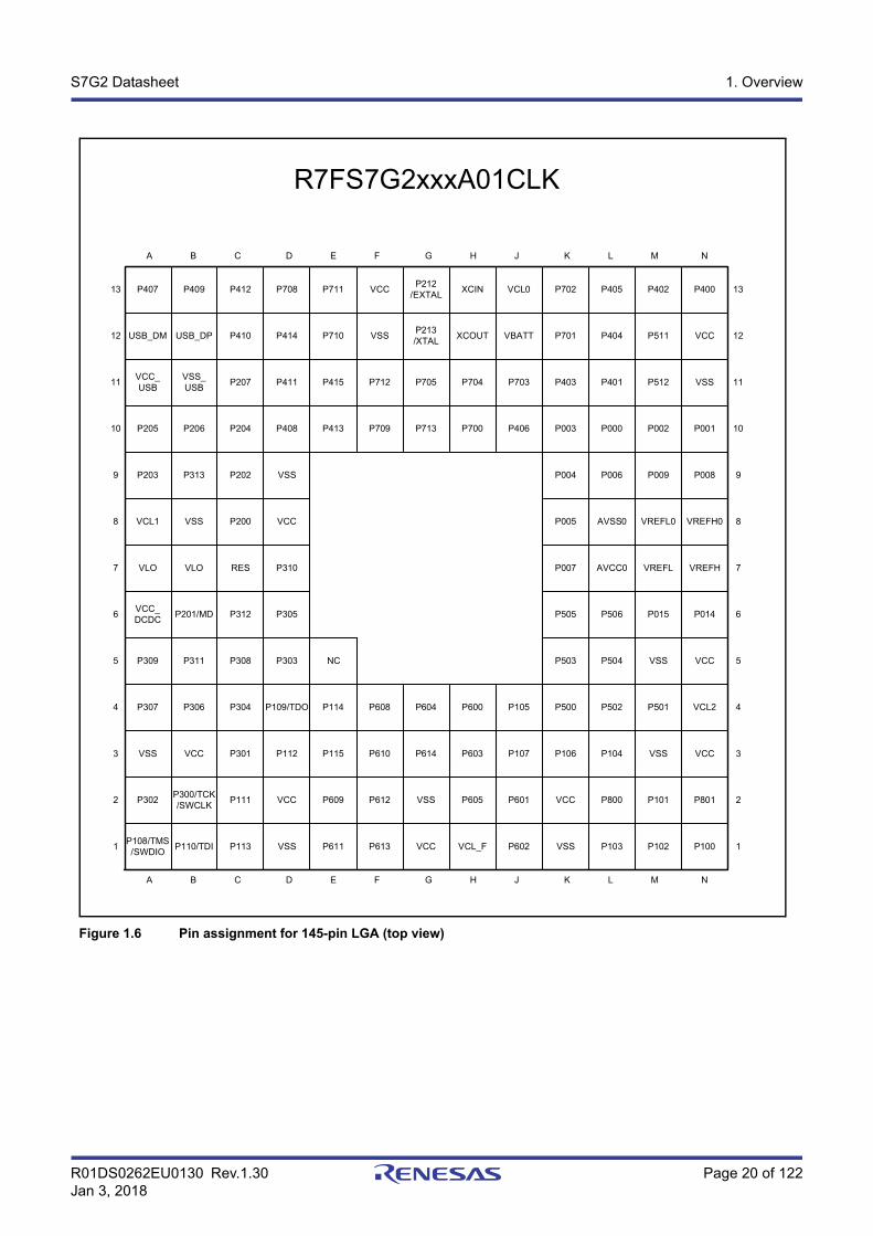
Figure 1.6 Pin assignment for 145-pin LGA (top view)
P400
VCC
VSS
P001
P008
VREFH0
VREFH
P014
VCC
VCL2
VCC
P801
P100
P402
P511
P512
P002
P009
VREFL0
VREFL
P015
VSS
P501
VSS
P101
P102
P405
P404
P401
P000
P006
AVSS0
AVCC0
P506
P504
P502
P104
P800
P103
P702
P701
P403
P003
P004
P005
P007
P505
P503
P500
P106
VCC
VSS
VCL0
VBATT
P703
P406
P105
P107
P601
P602
XCIN
XCOUT
P704
P700
P600
P603
P605
VCL_F
P212/EXTAL
P213/XTAL
P705
P713
P604
P614
VSS
VCC
VCC
VSS
P712
P709
P608
P610
P612
P613
P711
P710
P415
P413
P114
P115
P609
P611
P708
P414
P411
P408
VSS
VCC
P310
P305
P303
P109/TDO
P112
VCC
VSS
P412
P410
P207
P204
P202
P200
RES
P312
P308
P304
P301
P111
P113
P409
USB_DP
VSS_USB
P206
P313
VSS
VLO
P201/MD
P311
P306
VCC
P300/TCK/SWCLK
P110/TDI
P407
USB_DM
VCC_USB
P205
P203
VCL1
VLO
VCC_DCDC
P309
P307
VSS
P302
P108/TMS/SWDIO
R7FS7G2xxxA01CLK
13
12
11
10
9
8
7
6
5
4
3
2
1
13
12
11
10
9
8
7
6
5
4
3
2
1
N K L MG H JD E FA B C
N K L MG H JD E FA B C
NC
R01DS0262EU0130 Rev.1.30 Page 21 of 122Jan 3, 2018
S7G2 Datasheet 1. Overview
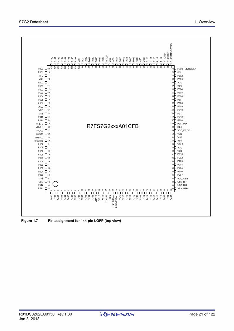
Figure 1.7 Pin assignment for 144-pin LQFP (top view)
1 2 3 4 5 6 7 8 9 10
11
12
13
14
15
16
17
18
19
20
21
22
23
24
25
26
27
28
29
30
31
32
33
34
35
36
108
107
106
105
104
103
102
101
100 99 98 97 96 95 94 93 92 91 90 89 88 87 86 85 84 83 82 81 80 79 78 77 76 75 74 73
72
71
70
69
68
67
66
65
64
63
62
61
60
59
58
57
56
55
54
53
52
51
50
49
48
47
46
45
44
43
42
41
40
39
38
37
109
110
111
112
113
114
115
116
117
118
119
120
121
122
123
124
125
126
127
128
129
130
131
132
133
134
135
136
137
138
139
140
141
142
143
144
VCC
VSS
P500
P501
P502
P503
P504
P505
P506
VCL2
VCC
VSS
P014
VREFLVREFH
AVCC0
AVSS0
VREFL0
VREFH0
P009
P008
P007
P006
P005
P004
P003
P002
P001
P000
VSS
VCC
P511
P801
P015
P512
P300/TCK/SWCLK
P302
P303
VCC
VSS
P304
P305
P306
P307
P308
P309
P310
P311
P200
P201/MD
RES
VCC_DCDC
VLO
VLO
VSS
VCL1
VCC
VSSP313
P202
P203
P204
P205
P206
P207
VCC_USB
USB_DP
VSS_USB
P301
P312
USB_DM
P10
0
P10
2
P10
3
P10
4
P10
5
P10
6
P10
7
VS
S
VC
C
P60
0
P60
1
P60
2
P60
3
P60
5
VC
L_F
VS
S
VC
C
P61
4
P61
3
P61
2
P61
1
P61
0
P60
9
P60
8
VS
S
VC
C
P11
5
P11
4
P11
3
P11
2
P11
1
P11
0/T
DI
P10
8/T
MS
/SW
DIO
P10
1
P60
4
P10
9/T
DO
P4
00
P4
02
P4
03
P4
04
P4
05
P4
06
P7
00
P7
01
P7
02
P7
03
P7
04
P7
05
VB
AT
T
XC
IN
XC
OU
T
VS
SP
21
3/X
TA
L
P21
2/E
XT
AL
VC
C
P7
13
P7
12
P7
11
P7
10
P7
08
P4
15
P4
14
P4
13
P4
12
P4
11
P41
0
P4
09
P4
07
P4
01
VC
L0
P4
08
P7
09
P800
R7FS7G2xxxA01CFB
R01DS0262EU0130 Rev.1.30 Page 22 of 122Jan 3, 2018
S7G2 Datasheet 1. Overview
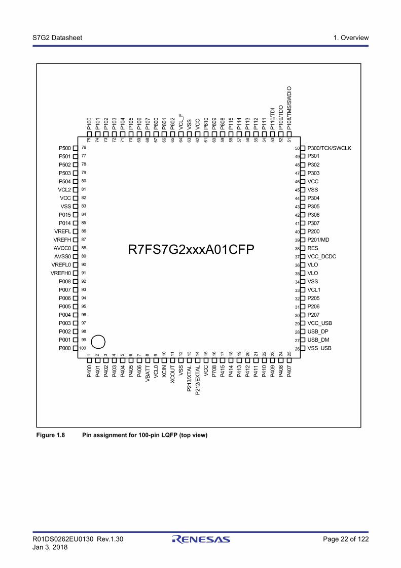
Figure 1.8 Pin assignment for 100-pin LQFP (top view)
1 2 3 4 5 6 7 8 9 10 11 12 13 14 15 16 17 18 19 20 21 22 23 24 25
75 74 73 72 71 70 69 68 67 66 65 64 63 62 61 60 59 58 57 56 55 54 53 52 51
50
49
48
47
46
45
44
43
42
41
40
39
38
37
36
35
34
33
32
31
30
29
28
27
26
76
77
78
79
80
81
82
83
84
85
86
87
88
89
90
91
92
93
94
95
96
97
98
99
100
P502
P503
P504
VCL2
VCC
VSS
P015
P014
VREFL
VREFH
AVCC0
AVSS0
VREFH0
P008
P007
P006
P005
P004
P003
P002
P001
P501
VREFL0
P300/TCK/SWCLK
P302
P303
VCC
VSS
P304
P305
P306
P307
P200
P201/MD
RES
VCC_DCDC
VLO
VSS
VCL1
P205
P206
P207
VCC_USB
USB_DP
USB_DM
VSS_USB
P301
VLO
P10
0
P10
2
P10
3
P10
4
P10
5
P10
6
P10
7
P60
0
P60
1
P60
2
VC
L_F
VS
S
VC
C
P60
9
P60
8
P11
5
P11
4
P11
3
P11
2
P11
1
P11
0/T
DI
P10
9/T
DO
P10
8/T
MS
/SW
DIO
P10
1
P61
0
P40
0
P40
2
P40
3
P40
4
P40
5
P40
6
VB
AT
T
VC
L0
XC
IN
XC
OU
T
VS
S
P21
3/X
TA
L
VC
C
P70
8
P41
5
P41
4
P41
3
P41
2
P41
1
P41
0
P40
9
P40
7
P40
1
P21
2/E
XT
AL
P500
P000
P40
8
R7FS7G2xxxA01CFP
R01DS0262EU0130 Rev.1.30 Page 23 of 122Jan 3, 2018
S7G2 Datasheet 1. Overview
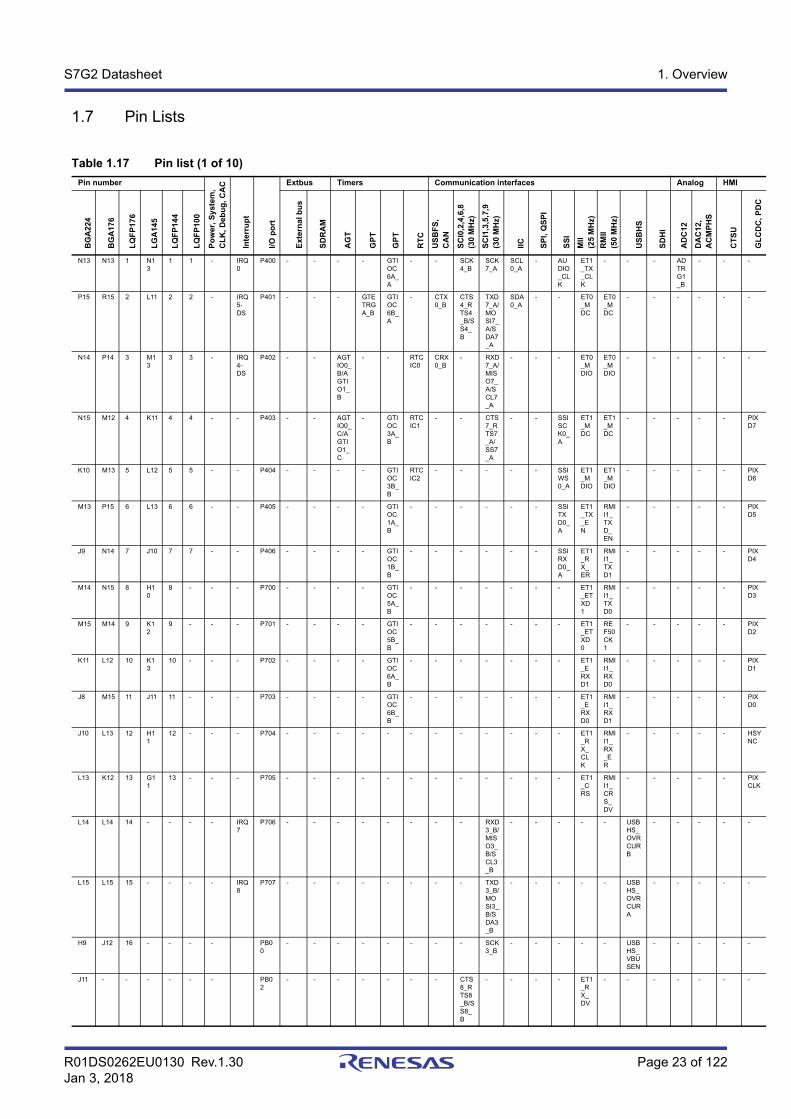
1.7 Pin Lists
Table 1.17 Pin list (1 of 10)
Pin number
Po
wer
, S
yst
em,
CL
K, D
ebu
g, C
AC
Inte
rru
pt
I/O
po
rt
Extbus Timers Communication interfaces Analog HMI
BG
A2
24
BG
A1
76
LQ
FP
176
LG
A14
5
LQ
FP
144
LQ
FP
100
Ext
ern
al b
us
SD
RA
M
AG
T
GP
T
GP
T
RT
C
US
BF
S,
CA
N
SC
I0,2
,4,6
,8(3
0 M
Hz)
SC
I1,3
,5,7
,9(3
0 M
Hz)
IIC
SP
I, Q
SP
I
SS
I
MII
(25
MH
z)
RM
II(5
0 M
Hz)
US
BH
S
SD
HI
AD
C12
DA
C12
,A
CM
PH
S
CT
SU
GL
CD
C,
PD
C
N13 N13 1 N13
1 1 - IRQ0
P400 - - - - GTIOC6A_A
- - SCK4_B
SCK7_A
SCL0_A
- AUDIO_CLK
ET1_TX_CLK
- - - ADTRG1_B
- - -
P15 R15 2 L11 2 2 - IRQ5-DS
P401 - - - GTETRGA_B
GTIOC6B_A
- CTX0_B
CTS4_RTS4_B/SS4_B
TXD7_A/MOSI7_A/SDA7_A
SDA0_A
- - ET0_MDC
ET0_MDC
- - - - - -
N14 P14 3 M13
3 3 - IRQ4-DS
P402 - - AGTIO0_B/AGTIO1_B
- - RTCIC0
CRX0_B
- RXD7_A/MISO7_A/SCL7_A
- - - ET0_MDIO
ET0_MDIO
- - - - - -
N15 M12 4 K11 4 4 - - P403 - - AGTIO0_C/AGTIO1_C
- GTIOC3A_B
RTCIC1
- - CTS7_RTS7_A/SS7_A
- - SSISCK0_A
ET1_MDC
ET1_MDC
- - - - - PIXD7
K10 M13 5 L12 5 5 - - P404 - - - - GTIOC3B_B
RTCIC2
- - - - - SSIWS0_A
ET1_MDIO
ET1_MDIO
- - - - - PIXD6
M13 P15 6 L13 6 6 - - P405 - - - - GTIOC1A_B
- - - - - - SSITXD0_A
ET1_TX_EN
RMII1_TXD_EN
- - - - - PIXD5
J9 N14 7 J10 7 7 - - P406 - - - - GTIOC1B_B
- - - - - - SSIRXD0_A
ET1_RX_ER
RMII1_TXD1
- - - - - PIXD4
M14 N15 8 H10
8 - - - P700 - - - - GTIOC5A_B
- - - - - - - ET1_ETXD1
RMII1_TXD0
- - - - - PIXD3
M15 M14 9 K12
9 - - - P701 - - - - GTIOC5B_B
- - - - - - - ET1_ETXD0
REF50CK1
- - - - - PIXD2
K11 L12 10 K13
10 - - - P702 - - - - GTIOC6A_B
- - - - - - - ET1_ERXD1
RMII1_RXD0
- - - - - PIXD1
J8 M15 11 J11 11 - - - P703 - - - - GTIOC6B_B
- - - - - - - ET1_ERXD0
RMII1_RXD1
- - - - - PIXD0
J10 L13 12 H11
12 - - - P704 - - - - - - - - - - - - ET1_RX_CLK
RMII1_RX_ER
- - - - - HSYNC
L13 K12 13 G11
13 - - - P705 - - - - - - - - - - - - ET1_CRS
RMII1_CRS_DV
- - - - - PIXCLK
L14 L14 14 - - - - IRQ7
P706 - - - - - - - - RXD3_B/MISO3_B/SCL3_B
- - - - - USBHS_OVRCURB
- - - - -
L15 L15 15 - - - - IRQ8
P707 - - - - - - - - TXD3_B/MOSI3_B/SDA3_B
- - - - - USBHS_OVRCURA
- - - - -
H9 J12 16 - - - - PB00
- - - - - - - - SCK3_B
- - - - - USBHS_VBUSEN
- - - - -
J11 - - - - - - PB02
- - - - - - - CTS8_RTS8_B/SS8_B
- - - - ET1_RX_DV
- - - - - - -
R01DS0262EU0130 Rev.1.30 Page 24 of 122Jan 3, 2018
S7G2 Datasheet 1. Overview
K12 - - - - - - PB03
- - - - - - - SCK8_B
- - - - ET1_COL
- - - - - - -
H10 - - - - - - IRQ12
PB04
- - - - - - - TXD8_B/MOSI8_B/SDA8_B
- - - - ET1_ERXD2
- - - - - - -
K13 K13 17 - - - - PB01
- - - - - - - - CTS3_RTS3_B/SS3_B
- - - - - USBHS_VBUS
- - - - -
J12 - - - - - - IRQ13
PB05
- - - - - - - RXD8_B/MISO8_B/SCL8_B
- - - - ET1_ERXD3
- - - - - - -
H11 - - - - - - - PB06
- - - - - - - - - - - ET1_WOL
ET1_WOL
- - - - - -
G11 - - - - - - - PB07
- - - - - - - - - - - ET1_LINKSTA
ET1_LINKSTA
- - - - - -
K14 K14 18 J12 14 8 VBATT
- - - - - - - - - - - - - - - - - - - - - -
K15 K15 19 J13 15 9 VCL0
- - - - - - - - - - - - - - - - - - - - - -
J15 J15 20 H13
16 10 XCIN
- - - - - - - - - - - - - - - - - - - - - -
J14 J14 21 H12
17 11 XCOUT
- - - - - - - - - - - - - - - - - - - - - -
J13 J13 22 F12 18 12 VSS - - - - - - - - - - - - - - - - - - - - - -
H14 H14 23 G12
19 13 XTAL
IRQ2
P213 - - - GTETRGC_A
- - - - TXD1_A/MOSI1_A/SDA1_A
- - - - - - - ADTRG1_A
- - -
H15 H15 24 G13
20 14 EXTAL
IRQ3
P212 - - AGTEE1
GTETRGD_A
- - - - RXD1_A/MISO1_A/SCL1_A
- - - - - - - - - - -
H12 H12 25 F13 21 15 VCC - - - - - - - - - - - - - - - - - - - - - -
H13 H13 26 - - - AVCC_USBHS
- - - - - - - - - - - - - - - - - - - - - -
G13 G13 27 - - - USBHS_RREF
- - - - - - - - - - - - - - - - - - - - - -
G14 G14 28 - - - AVSS_USBHS
- - - - - - - - - - - - - - - - - - - - - -
G15 G15 29 - - - PVSS_USBHS
- - - - - - - - - - - - - - - - - - - - - -
G12 G12 30 - - - VSS2_USBHS
- - - - - - - - - - - - - - - - - - - - - -
F15 F15 31 - - - - - - - - - - - - - - - - - - - - USBHS_DM
- - - - -
F14 F14 32 - - - - - - - - - - - - - - - - - - - - USBHS_DP
- - - - -
F12 F12 33 - - - VSS1_USBHS
- - - - - - - - - - - - - - - - - - - - - -
F13 F13 34 - - - VCC_USBHS
- - - - - - - - - - - - - - - - - - - - - -
E15 E15 35 - - - VSS - - - - - - - - - - - - - - - - - - - - -
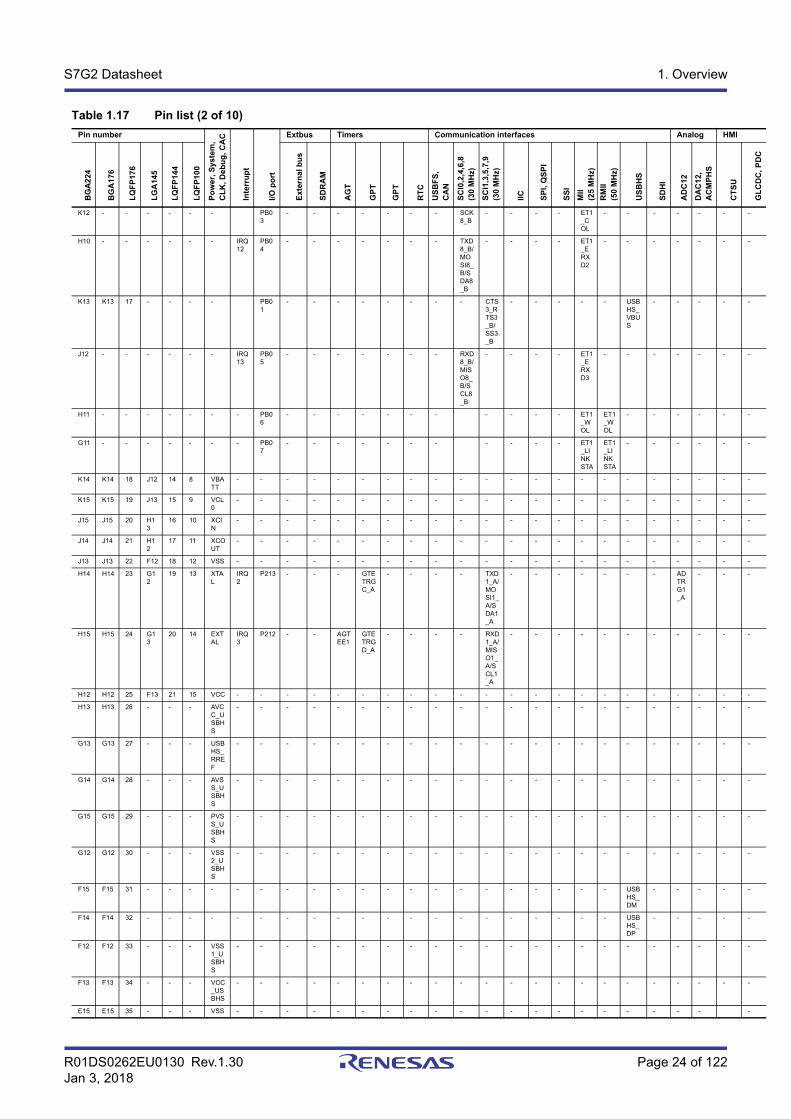
Table 1.17 Pin list (2 of 10)
Pin number
Po
wer
, S
yst
em,
CL
K, D
ebu
g, C
AC
Inte
rru
pt
I/O
po
rt
Extbus Timers Communication interfaces Analog HMI
BG
A2
24
BG
A1
76
LQ
FP
176
LG
A14
5
LQ
FP
144
LQ
FP
100
Ext
ern
al b
us
SD
RA
M
AG
T
GP
T
GP
T
RT
C
US
BF
S,
CA
N
SC
I0,2
,4,6
,8(3
0 M
Hz)
SC
I1,3
,5,7
,9(3
0 M
Hz)
IIC
SP
I, Q
SP
I
SS
I
MII
(25
MH
z)
RM
II(5
0 M
Hz)
US
BH
S
SD
HI
AD
C12
DA
C12
,A
CM
PH
S
CT
SU
GL
CD
C,
PD
C
R01DS0262EU0130 Rev.1.30 Page 25 of 122Jan 3, 2018
S7G2 Datasheet 1. Overview
G10 - - G10
22 - - - P713 - - - - GTIOC2A_B
- - - - - - - ET1_EXOUT
ET1_EXOUT
- - - - TS17
-
F11 - - F11 23 - - - P712 - - - - GTIOC2B_B
- - - - - - - - - - - - - TS16
-
E12 - - E13
24 - - - P711 - - - - - - - - CTS1_RTS1_B/SS1_B
- - - ET0_TX_CLK
- - - - - TS15
-
F10 - - E12
25 - - - P710 - - - - - - - - SCK1_B
- - - ET0_TX_ER
- - - - - TS14
-
E13 - - F10 26 - - IRQ10
P709 - - - - - - - - TXD1_B/MOSI1_B/SDA1_B
- - - ET0_ETXD2
- - - - - TS13
-
D15 - - D13
27 16 CACREF_B
IRQ11
P708 - - - - - - - - RXD1_B/MISO1_B/SCL1_B
- SSLA3_B
- ET0_ETXD3
- - - - - TS12
-
E14 E14 36 E11 28 17 - - P415 - - - - - - - - - - SSLA2_B
- ET0_TX_EN
RMII0_TXD_EN
- - - - TS11
-
E11 D15 37 D12
29 18 - - P414 - - - - - - - - - - SSLA1_B
- ET0_RX_ER
RMII0_TXD1
- SD0WP
- - TS10
-
D12 E13 38 E10
30 19 - - P413 - - - GTOUUP_B
- - - CTS0_RTS0_B/SS0_B
- - SSLA0_B
- ET0_ETXD1
RMII0_TXD0
- SD0CLK
- - TS09
-
D13 D14 39 C13
31 20 - - P412 - - - GTOULO_B
- - - SCK0_B
- - RSPCKA_B
- ET0_ETXD0
REF50CK0
- SD0CMD
- - TS08
-
D14 C15 40 D11
32 21 - IRQ4
P411 - - AGTOA1
GTOVUP_B
GTIOC9A_A
- - TXD0_B/MOSI0_B/SDA0_B
CTS3_RTS3_A/SS3_A
- MOSIA_B
- ET0_ERXD1
RMII0_RXD0
- SD0DAT0
- - TS07
-
C15 C14 41 C12
33 22 - IRQ5
P410 - - AGTOB1
GTOVLO_B
GTIOC9B_A
- - RXD0_B/MISO0_B/SCL0_B
SCK3_A
- MISOA_B
- ET0_ERXD0
RMII0_RXD1
- SD0DAT1
- - TS06
-
C14 B15 42 B13
34 23 - IRQ6
P409 - - - GTOWUP_B
GTIOC10A_A
- USB_EXICEN_A
- TXD3_A/MOSI3_A/SDA3_A
- - - ET0_RX_CLK
RMII0_RX_ER
USBHS_EXICEN
- - - TS05
-
B15 D13 43 D10
35 24 - IRQ7
P408 - - - GTOWLO_B
GTIOC10B_A
- USB_ID_A
- RXD3_A/MISO3_A/SCL3_A
- - - ET0_CRS
RMII0_CRS_DV
USBHS_ID
- - - TS04
-
A15 A15 44 A13
36 25 - - P407 - - - - - RTCOUT
USB_VBUS
CTS4_RTS4_A/SS4_A
- SDA0_B
SSLB3_A
- ET0_EXOUT
ET0_EXOUT
- - ADTRG0
- TS03
-
B13 C13 45 B11 37 26 VSS_USB
- - - - - - - - - - - - - - - - - - - - - -
B14 B14 46 A12
38 27 - - - - - - - - USB_DM
- - - - - - - - - - - - -
A14 A14 47 B12
39 28 - - - - - - - - USB_DP
- - - - - - - - - - - - -
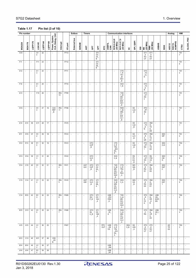
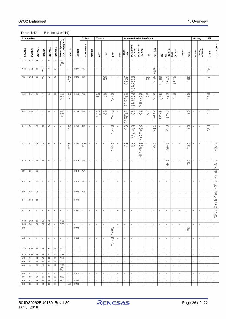
Table 1.17 Pin list (3 of 10)
Pin number
Po
wer
, S
yst
em,
CL
K, D
ebu
g, C
AC
Inte
rru
pt
I/O
po
rt
Extbus Timers Communication interfaces Analog HMI
BG
A2
24
BG
A1
76
LQ
FP
176
LG
A14
5
LQ
FP
144
LQ
FP
100
Ext
ern
al b
us
SD
RA
M
AG
T
GP
T
GP
T
RT
C
US
BF
S,
CA
N
SC
I0,2
,4,6
,8(3
0 M
Hz)
SC
I1,3
,5,7
,9(3
0 M
Hz)
IIC
SP
I, Q
SP
I
SS
I
MII
(25
MH
z)
RM
II(5
0 M
Hz)
US
BH
S
SD
HI
AD
C12
DA
C12
,A
CM
PH
S
CT
SU
GL
CD
C,
PD
C
R01DS0262EU0130 Rev.1.30 Page 26 of 122Jan 3, 2018
S7G2 Datasheet 1. Overview
A13 B13 48 A11 40 29 VCC_USB
- - - - - - - - - - - - - - - - - - - - - -
C13 C12 49 C11
41 30 - - P207 A17 - - - - - - - - - SSLB2_A
- - - - - - - TS02
-
G9 D12 50 B10
42 31 - IRQ0-DS
P206 WAIT - - GTIU_A
- - USB_VBUSEN_A
RXD4_A/MISO4_A/SCL4_A
- SDA1_A
SSLB1_A
SSIDATA1_A
ET0_LINKSTA
ET0_LINKSTA
- SD0DAT2
- - TS01
-
C12 E12 51 A10
43 32 CLKOUT_A
IRQ1-DS
P205 A16 - AGTO1
GTIV_A
GTIOC4A_B
- USB_OVRCURA_A-DS
TXD4_A/MOSI4_A/SDA4_A
CTS9_RTS9_A/SS9_A
SCL1_A
SSLB0_A
SSIWS1_A
ET0_WOL
ET0_WOL
- SD0DAT3
- - TSCAP_A
-
D11 A13 52 C10
44 - CACREF_A
- P204 A18 - AGTIO1_A
GTIW_A
GTIOC4B_B
- USB_OVRCURB_A-DS
SCK4_A
SCK9_A
SCL0_B
RSPCKB_A
SSISCK1_A
ET0_RX_DV
- - SD0DAT4
- - TS00
-
B12 D11 53 A9 45 - - IRQ2-DS
P203 A19 - - - GTIOC5A_A
- CTX0_A
CTS2_RTS2_A/SS2_A
TXD9_A/MOSI9_A/SDA9_A
- MOSIB_A
- ET0_COL
- - SD0DAT5
- - TSCAP_B
-
A12 B12 54 C9 46 - - IRQ3-DS
P202 WR1/BC1
- - - GTIOC5B_A
- CRX0_A
SCK2_A
RXD9_A/MISO9_A/SCL9_A
- MISOB_A
ET0_ERXD2
- - SD0DAT6
- - - LCD_TCON3_B
E10 A12 55 B9 47 - - - P313 A20 - - - - - - - - - - - ET0_ERXD3
- - SD0DAT7
- - - LCD_TCON2_B
F9 C11 56 - - - - - P314 A21 - - - - - - - - - - - - - - - - - - LCD_TCON1_B
C11 B11 57 - - - - - P315 A22 - - - - - - - - - - - - - - - - - - LCD_TCON0_B
E9 A11 58 - - - - - P900 A23 - - - - - - - - - - - - - - - - - - LCD_CLK_B
B11 C10 59 - - - - - P901 - - - - - - - - - - - - - - - - - - LCD_DATA15_B
A11 - - - - - - - P902 - - - - - - - - - - - - - - - - - - - LCD_DATA23_B
C10 D10 60 D9 48 - VSS - - - - - - - - - - - - - - - - - - - - - -
D10 D9 61 D8 49 - VCC - - - - - - - - - - - - - - - - - - - - - -
D9 - - - - - - - P903 - - - - GTIOC7A_B
- - - - - - - - - - SD0CD
- - - -
C9 - - - - - - - P904 - - - - GTIOC7B_B
- - - - - - - - - - - - - - -
A10 A10 62 A8 50 33 VCL1
- - - - - - - - - - - - - - - - - - - - - -
B10 B10 63 B8 51 34 VSS - - - - - - - - - - - - - - - - - - - - - -
A9 A9 64 A7 52 35 VLO - - - - - - - - - - - - - - - - - - - - - -
B9 B9 65 B7 53 36 VLO - - - - - - - - - - - - - - - - - - - - - -
A8 A8 66 A6 54 37 VCC_DCDC
- - - - - - - - - - - - - - - - - - - - - -
H8 - - - - - - P913 - - - - - - - - - - - - - - - - - - - -
F8 C9 67 C7 55 38 RES - - - - - - - - - - - - - - - - - - - - -
C8 B8 68 B6 56 39 MD - P201 - - - - - - - - - - - - - - - - - - - -
B8 C8 69 C8 57 40 - NMI P200 - - - - - - - - - - - - - - - - - - - -
Table 1.17 Pin list (4 of 10)
Pin number
Po
wer
, S
yst
em,
CL
K, D
ebu
g, C
AC
Inte
rru
pt
I/O
po
rt
Extbus Timers Communication interfaces Analog HMI
BG
A2
24
BG
A1
76
LQ
FP
176
LG
A14
5
LQ
FP
144
LQ
FP
100
Ext
ern
al b
us
SD
RA
M
AG
T
GP
T
GP
T
RT
C
US
BF
S,
CA
N
SC
I0,2
,4,6
,8(3
0 M
Hz)
SC
I1,3
,5,7
,9(3
0 M
Hz)
IIC
SP
I, Q
SP
I
SS
I
MII
(25
MH
z)
RM
II(5
0 M
Hz)
US
BH
S
SD
HI
AD
C12
DA
C12
,A
CM
PH
S
CT
SU
GL
CD
C,
PD
C
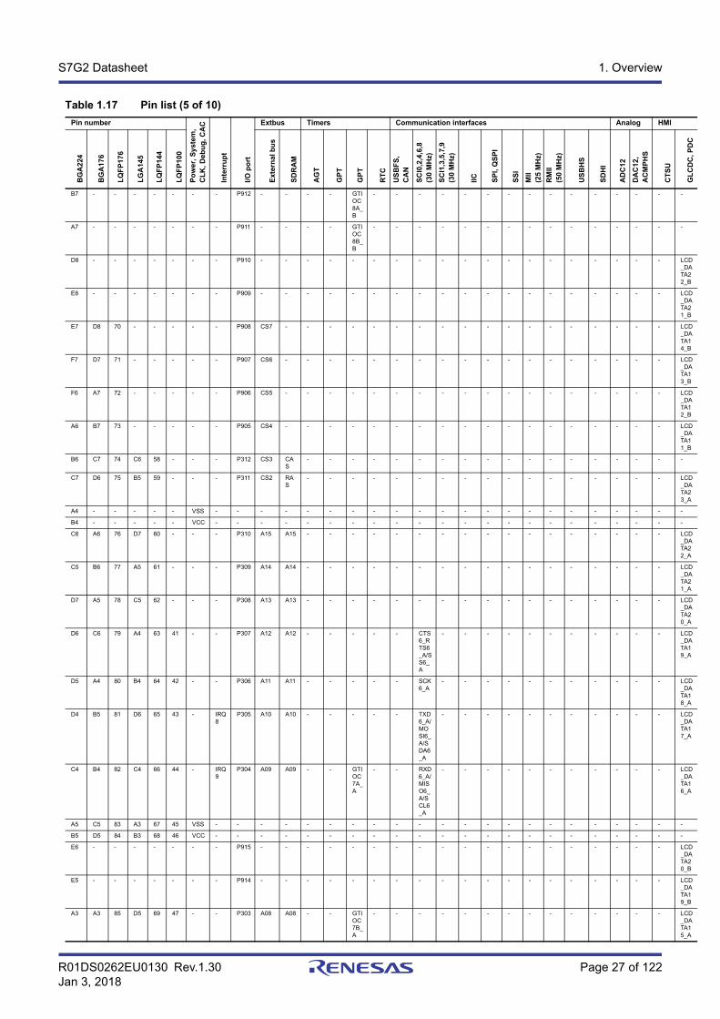
R01DS0262EU0130 Rev.1.30 Page 27 of 122Jan 3, 2018
S7G2 Datasheet 1. Overview
B7 - - - - - - - P912 - - - - GTIOC8A_B
- - - - - - - - - - - - - - -
A7 - - - - - - - P911 - - - - GTIOC8B_B
- - - - - - - - - - - - - - -
D8 - - - - - - - P910 - - - - - - - - - - - - - - - - - - - LCD_DATA22_B
E8 - - - - - - - P909 - - - - - - - - - - - - - - - - - - - LCD_DATA21_B
E7 D8 70 - - - - - P908 CS7 - - - - - - - - - - - - - - - - - - LCD_DATA14_B
F7 D7 71 - - - - - P907 CS6 - - - - - - - - - - - - - - - - - - LCD_DATA13_B
F6 A7 72 - - - - - P906 CS5 - - - - - - - - - - - - - - - - - - LCD_DATA12_B
A6 B7 73 - - - - - P905 CS4 - - - - - - - - - - - - - - - - - - LCD_DATA11_B
B6 C7 74 C6 58 - - - P312 CS3 CAS
- - - - - - - - - - - - - - - - - -
C7 D6 75 B5 59 - - - P311 CS2 RAS
- - - - - - - - - - - - - - - - - LCD_DATA23_A
A4 - - - - - VSS - - - - - - - - - - - - - - - - - - - - - -
B4 - - - - - VCC - - - - - - - - - - - - - - - - - - - - - -
C6 A6 76 D7 60 - - - P310 A15 A15 - - - - - - - - - - - - - - - - - LCD_DATA22_A
C5 B6 77 A5 61 - - - P309 A14 A14 - - - - - - - - - - - - - - - - - LCD_DATA21_A
D7 A5 78 C5 62 - - - P308 A13 A13 - - - - - - - - - - - - - - - - - LCD_DATA20_A
D6 C6 79 A4 63 41 - - P307 A12 A12 - - - - - CTS6_RTS6_A/SS6_A
- - - - - - - - - - - LCD_DATA19_A
D5 A4 80 B4 64 42 - - P306 A11 A11 - - - - - SCK6_A
- - - - - - - - - - - LCD_DATA18_A
D4 B5 81 D6 65 43 - IRQ8
P305 A10 A10 - - - - - TXD6_A/MOSI6_A/SDA6_A
- - - - - - - - - - - LCD_DATA17_A
C4 B4 82 C4 66 44 - IRQ9
P304 A09 A09 - - GTIOC7A_A
- - RXD6_A/MISO6_A/SCL6_A
- - - - - - - - - - - LCD_DATA16_A
A5 C5 83 A3 67 45 VSS - - - - - - - - - - - - - - - - - - - - - -
B5 D5 84 B3 68 46 VCC - - - - - - - - - - - - - - - - - - - - - -
E6 - - - - - - - P915 - - - - - - - - - - - - - - - - - - - LCD_DATA20_B
E5 - - - - - - - P914 - - - - - - - - - - - - - - - - - - - LCD_DATA19_B
A3 A3 85 D5 69 47 - - P303 A08 A08 - - GTIOC7B_A
- - - - - - - - - - - - - - LCD_DATA15_A
Table 1.17 Pin list (5 of 10)
Pin number
Po
wer
, S
yst
em,
CL
K, D
ebu
g, C
AC
Inte
rru
pt
I/O
po
rt
Extbus Timers Communication interfaces Analog HMI
BG
A2
24
BG
A1
76
LQ
FP
176
LG
A14
5
LQ
FP
144
LQ
FP
100
Ext
ern
al b
us
SD
RA
M
AG
T
GP
T
GP
T
RT
C
US
BF
S,
CA
N
SC
I0,2
,4,6
,8(3
0 M
Hz)
SC
I1,3
,5,7
,9(3
0 M
Hz)
IIC
SP
I, Q
SP
I
SS
I
MII
(25
MH
z)
RM
II(5
0 M
Hz)
US
BH
S
SD
HI
AD
C12
DA
C12
,A
CM
PH
S
CT
SU
GL
CD
C,
PD
C
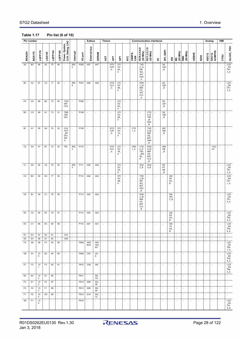
R01DS0262EU0130 Rev.1.30 Page 28 of 122Jan 3, 2018
S7G2 Datasheet 1. Overview
A2 B3 86 A2 70 48 - IRQ5
P302 A07 A07 - GTOUUP_A
GTIOC4A_A
- - TXD2_A/MOSI2_A/SDA2_A
- - SSLB3_B
- - - - - - - - LCD_DATA14_A
B3 A2 87 C3 71 49 - IRQ6
P301 A06 A06 - GTOULO_A
GTIOC4B_A
- - RXD2_A/MISO2_A/SCL2_A
- - SSLB2_B
- - - - - - - - LCD_DATA13_A
F5 C4 88 B2 72 50 TCK/SWCLK
- P300 - - - - GTIOC0A_A
- - - - - SSLB1_B
- - - - - - - - -
B2 C3 89 A1 73 51 TMS/SWDIO
- P108 - - - - GTIOC0B_A
- - - CTS9_RTS9_B/SS9_B
- SSLB0_B
- - - - - - - - -
B1 A1 90 D4 74 52 CLKOUT_B/TDO/SWO
- P109 - - - GTOVUP_A
GTIOC1A_A
- CTX1_A
- TXD9_B/MISO9_B/SDA9_B
- MOSIB_B
- - - - - - - - -
C2 D3 91 B1 75 53 TDI IRQ3
P110 - - - GTOVLO_A
GTIOC1B_A
- CRX1_A
CTS2_RTS2_B/SS2_B
RXD9_B/MISO9_B/SCL9_B
- MISOB_B
- - - - - - VCOUT
- -
C1 D4 92 C2 76 54 - IRQ4
P111 A05 A05 - - GTIOC3A_A
- - SCK2_B
SCK9_B
- RSPCKB_B
- - - - - - - - LCD_DATA12_A
C3 B2 93 D3 77 55 - - P112 A04 A04 - - GTIOC3B_A
- - TXD2_B/MOSI2_B/SDA2_B
- - - SSISCK0_B
- - - - - - LCD_DATA11_A
D3 B1 94 C1 78 56 - - P113 A03 A03 - - - - - RXD2_B/MISO2_B/SCL2_B
- - - SSIWS0_B
- - - - - - LCD_DATA10_A
E4 C2 95 E4 79 57 - - P114 A02 A02 - - - - - - - - - SSIRXD0_B
- - - - - - LCD_DATA09_A
E3 C1 96 E3 80 58 - - P115 A01 A01 - - - - - - - - - SSITXD0_B
- - - - - - LCD_DATA08_A
D1 E3 97 D2 81 - VCC - - - - - - - - - - - - - - - - - - - - -
D2 E4 98 D1 82 - VSS - - - - - - - - - - - - - - - - - - - - -
F4 D2 99 F4 83 59 - - P608 A00/BC0
A00/DQM1
- - - - - - - - - - - - - - - - - LCD_DATA07_A
G4 D1 100
E2 84 60 - - P609 CS1 CKE
- - - - - - - - - - - - - - - - - LCD_DATA06_A
E1 F3 101
F3 85 61 - - P610 CS0 WE - - - - - - - - - - - - - - - - - LCD_DATA05_A
E2 E2 102
E1 86 - - - P611 SDCS
- - - - - - - - - - - - - - - - - -
F2 E1 103
F2 87 - - - P612 D08 DQ08
- - - - - - - - - - - - - - - - - -
F3 F4 104
F1 88 - - - P613 D09 DQ09
- - - - - - - - - - - - - - - - - -
F1 F2 105
G3 89 - - - P614 D10 DQ10
- - - - - - - - - - - - - - - - - -
G8 F1 106
- - - - - P615 - - - - - - - - - - - - - - - - - - - LCD_DATA10_B
Table 1.17 Pin list (6 of 10)
Pin number
Po
wer
, S
yst
em,
CL
K, D
ebu
g, C
AC
Inte
rru
pt
I/O
po
rt
Extbus Timers Communication interfaces Analog HMI
BG
A2
24
BG
A1
76
LQ
FP
176
LG
A14
5
LQ
FP
144
LQ
FP
100
Ext
ern
al b
us
SD
RA
M
AG
T
GP
T
GP
T
RT
C
US
BF
S,
CA
N
SC
I0,2
,4,6
,8(3
0 M
Hz)
SC
I1,3
,5,7
,9(3
0 M
Hz)
IIC
SP
I, Q
SP
I
SS
I
MII
(25
MH
z)
RM
II(5
0 M
Hz)
US
BH
S
SD
HI
AD
C12
DA
C12
,A
CM
PH
S
CT
SU
GL
CD
C,
PD
C
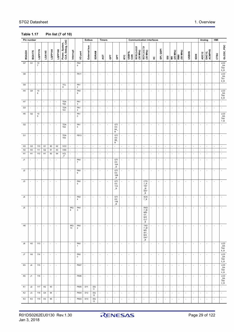
R01DS0262EU0130 Rev.1.30 Page 29 of 122Jan 3, 2018
S7G2 Datasheet 1. Overview
G7 G1 107
- - - - - PA08
- - - - - - - - - - - - - - - - - - - LCD_DATA09_B
G6 - - - - - - - PA11 - - - - - - - - - - - - - - - - - - - LCD_DATA18_B
G5 - - - - - TCLK
- PA12
- - - - - - - - - - - - - - - - - - -
H4 G4 108
- - - - - PA09
- - - - - - - - - - - - - - - - - - - LCD_DATA08_B
H7 - - - - - TDATA0
- PA13
- - - - - - - - - - - - - - - - - - - -
G3 - - - - - TDATA1
- PA14
- - - - - - - - - - - - - - - - - - - -
H5 G2 109
- - - - - PA10
- - - - - - - - - - - - - - - - - - - LCD_DATA07_B
G2 - - - - - TDATA2
- PA15
- - - - GTIOC9A_B
- - - - - - - - - - - - - - -
G1 - - - - - TDATA3
- P813 - - - - GTIOC9B_B
- - - - - - - - - - - - - - -
H3 G3 110 G1 90 62 VCC - - - - - - - - - - - - - - - - - - - - - -
H2 H3 111 G2 91 63 VSS - - - - - - - - - - - - - - - - - - - - - -
H1 H1 112 H1 92 64 VCL_F
- - - - - - - - - - - - - - - - - - - - - -
J1 - - - - - - PA07
- - - - GTIOC10A_B
- - - - - - - - - - - - - - -
J2 - - - - - - PA06
- - - - GTIOC10B_B
- - - - - - - - - - - - - - -
J3 - - - - - - PA05
- - - - GTIOC11A_B
- - - CTS7_RTS7_B/SS7_B
- - - - - - - - - - -
J4 - - - - - - PA04
- - - - GTIOC11B_B
- - - SCK7_B
- - - - - - - - - - -
J5 - - - - - IRQ9
PA03
- - - - - - - - RXD7_B/MISO7_B/SCL7_B
- - - - - - - - - - -
H6 - - - - - IRQ10
PA02
- - - - - - - - TXD7_B/MOSI7_B/SDA7_B
- - - - - - - - - - -
J6 H2 113 - - - - PA01
- - - - - - - - - - - - - - - - - - - LCD_DATA06_B
J7 H4 114 - - - - PA00
- - - - - - - - - - - - - - - - - - - LCD_DATA05_B
K5 J4 115 - - - - P607 - - - - - - - - - - - - - - - - - - - LCD_DATA04_B
K6 J1 116 - - - - P606 - - - - - - - - - - - - - - - - - - - LCD_DATA03_B
K1 J2 117 H2 93 - - P605 D11 DQ11
- - - - - - - - - - - - - - - - - -
K2 J3 118 G4 94 - - P604 D12 DQ12
- - - - - - - - - - - - - - - - - -
K3 K3 119 H3 95 - - P603 D13 DQ13
- - - - - - - - - - - - - - - - - -
Table 1.17 Pin list (7 of 10)
Pin number
Po
wer
, S
yst
em,
CL
K, D
ebu
g, C
AC
Inte
rru
pt
I/O
po
rt
Extbus Timers Communication interfaces Analog HMI
BG
A2
24
BG
A1
76
LQ
FP
176
LG
A14
5
LQ
FP
144
LQ
FP
100
Ext
ern
al b
us
SD
RA
M
AG
T
GP
T
GP
T
RT
C
US
BF
S,
CA
N
SC
I0,2
,4,6
,8(3
0 M
Hz)
SC
I1,3
,5,7
,9(3
0 M
Hz)
IIC
SP
I, Q
SP
I
SS
I
MII
(25
MH
z)
RM
II(5
0 M
Hz)
US
BH
S
SD
HI
AD
C12
DA
C12
,A
CM
PH
S
CT
SU
GL
CD
C,
PD
C
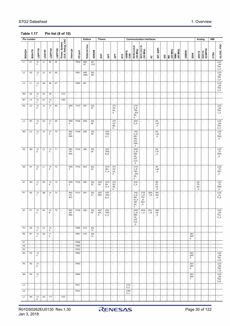
R01DS0262EU0130 Rev.1.30 Page 30 of 122Jan 3, 2018
S7G2 Datasheet 1. Overview
L1 K1 120
J1 96 65 - P602 EBCLK
SDCLK
- - - - - - - - - - - - - - - - - LCD_DATA04_A
L2 K2 121
J2 97 66 - - P601 WR/WR0
DQM0
- - - - - - - - - - - - - - - - - LCD_DATA03_A
L3 L1 122
H4 98 67 - - P600 RD - - - - - - - - - - - - - - - - - - LCD_DATA02_A
M2 K4 123
K2 99 - VCC - - - - - - - - - - - - - - - - - - - - - -
M1 L4 124
K1 100
- VSS - - - - - - - - - - - - - - - - - - - - - -
K4 L2 125
J3 101
68 - KR07
P107 D07 DQ07
- - GTIOC8A_A
- - CTS8_RTS8_A/SS8_A
- - - - - - - - - - - LCD_DATA01_A
L4 M1 126
K3 102
69 - KR06
P106 D06 DQ06
- - GTIOC8B_A
- - SCK8_A
- - SSLA3_A
- - - - - - - - LCD_DATA00_A
M3 L3 127
J4 103
70 - IRQ0/KR05
P105 D05 DQ05
- GTETRGA_C
- - - TXD8_A/MOSI8_A/SDA8_A
- - SSLA2_A
- - - - - - - - LCD_TCON3_A
N3 M2 128
L3 104
71 - IRQ1/KR04
P104 D04 DQ04
- GTETRGB_B
- - - RXD8_A/MISO8_A/SCL8_A
- - SSLA1_A
- - - - - - - - LCD_TCON2_A
N2 N1 129
L1 105
72 - KR03
P103 D03 DQ03
- GTOWUP_A
GTIOC2A_A
- - CTS0_RTS0_A/SS0_A
- - SSLA0_A
- - - - - - - - LCD_TCON1_A
N1 M3 130
M1 106
73 - KR02
P102 D02 DQ02
AGTO0
GTOWLO_A
GTIOC2B_A
- - SCK0_A
- - RSPCKA_A
- - - - - ADTRG0_A
- - LCD_TCON0_A
P1 N2 131
M2 107
74 - IRQ1/KR01
P101 D01 DQ01
AGTEE0
GTETRGB_A
- - - TXD0_A/MOSI_A/SDA0_A
CTS1_RTS1_A/SS1_A
SDA1_B
MOSIA_A
- - - - - - - - LCD_CLK_A
R1 P1 132
N1 108
75 - IRQ2/KR00
P100 D00 DQ00
AGTIO0_A
GTETRGA_A
- - - RXD0_A/MISO0_A/SCL0_A
SCK1_A
SCL1_B
MISOA_A
- - - - - - - - LCD_EXTCLK_A
P2 N3 133
L2 109
- - - P800 D14 DQ14
- - - - - - - - - - - - - - - - - -
R2 R1 134
N2 110
- - - P801 D15 DQ15
- - - - - - - - - - - - - SD1DAT4
- - - -
K7 - - - - - - - P808 - - - - - - - - - - - - - - - - - - - -
K8 - - - - - - - P809 - - - - - - - - - - - - - - - - - - - -
P3 - - - - - - - P810 - - - - - - - - - - - - - - - - - - - -
R3 P2 135
- - - - - P802 - - - - - - - - - - - - - - - SD1DAT5
- - - LCD_DATA02_B
P4 R2 136
- - - - - P803 - - - - - - - - - - - - - - - SD1DAT6
- - - LCD_DATA01_B
M4 P3 137
- - - - P804 - - - - - - - - - - - - - - - SD1DAT7
- - - LCD_DATA00_B
L5 - - - - - - P811 - - - - - - CTX0_C
- - - - - - - - - - - - -
L6 - - - - - - P812 - - - - - - CRX0_C
- - - - - - - - - - - - -
L7 N4 138
N3 111 - VCC - - - - - - - - - - - - - - - - - - - -
Table 1.17 Pin list (8 of 10)
Pin number
Po
wer
, S
yst
em,
CL
K, D
ebu
g, C
AC
Inte
rru
pt
I/O
po
rt
Extbus Timers Communication interfaces Analog HMI
BG
A2
24
BG
A1
76
LQ
FP
176
LG
A14
5
LQ
FP
144
LQ
FP
100
Ext
ern
al b
us
SD
RA
M
AG
T
GP
T
GP
T
RT
C
US
BF
S,
CA
N
SC
I0,2
,4,6
,8(3
0 M
Hz)
SC
I1,3
,5,7
,9(3
0 M
Hz)
IIC
SP
I, Q
SP
I
SS
I
MII
(25
MH
z)
RM
II(5
0 M
Hz)
US
BH
S
SD
HI
AD
C12
DA
C12
,A
CM
PH
S
CT
SU
GL
CD
C,
PD
C
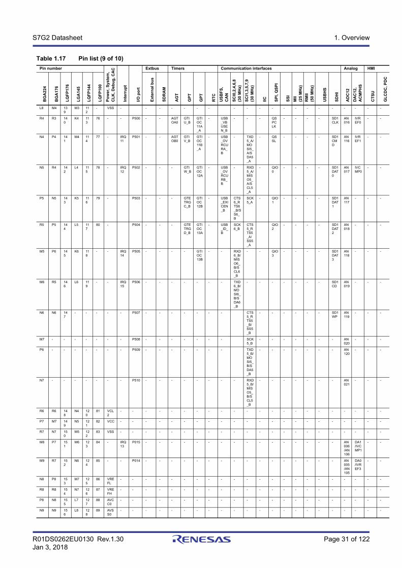
R01DS0262EU0130 Rev.1.30 Page 31 of 122Jan 3, 2018
S7G2 Datasheet 1. Overview
L8 M4 139
M3 112
- VSS - - - - - - - - - - - - - - - - - - - -
R4 R3 140
K4 113
76 - - P500 - - AGTOA0
GTIU_B
GTIOC11A_A
- USB_VBUSEN_B
- - - QSPCLK
- - - - SD1CLK
AN016
IVREF0
- -
N4 P4 141
M4 114
77 - IRQ11
P501 - - AGTOB0
GTIV_B
GTIOC11B_A
- USB_OVRCURA_B
- TXD5_A/MOSI5_A/SDA5_A
- QSSL
- - - - SD1CMD
AN116
IVREF1
- -
N5 R4 142
L4 115
78 - IRQ12
P502 - - - GTIW_B
GTIOC12A
- USB_OVRCURB_B
- RXD5_A/MISO5_A/SCL5_A
- QIO0
- - - - SD1DAT0
AN017
IVCMP0
- -
P5 N5 143
K5 116
79 - P503 - - - GTETRGC_B
GTIOC12B
- USB_EXICEN_B
CTS6_RTS6_B/SS6_B
SCK5_A
- QIO1
- - - - SD1DAT1
AN117
- - -
R5 P5 144
L5 117
80 - P504 - - - GTETRGD_B
GTIOC13A
- USB_ID_B
SCK6_B
CTS5_RTS5_A/SS5_A
QIO2
- - - - SD1DAT2
AN018
- - -
M5 P6 145
K6 118
- - IRQ14
P505 - - - - GTIOC13B
- - RXD6_B/MISO6_B/SCL6_B
- - QIO3
- - - - SD1DAT3
AN118
- - -
M6 R5 146
L6 119
- - IRQ15
P506 - - - - - - - TXD6_B/MOSI6_B/SDA6_B
- - - - - - - SD1CD
AN019
- - -
N6 N6 147
- - - - - P507 - - - - - - - CTS5_RTS5_B/SS5_B
- - - - - - SD1WP
AN119
- - -
M7 - - - - - - - P508 - - - - - - - SCK5_B
- - - - - - - AN020
- - -
P6 - - - - - - - P509 - - - - - - - TXD5_B/MOSI5_B/SDA5_B
- - - - - - - AN120
- - -
N7 - - - - - - - P510 - - - - - - - - RXD5_B/MISO5_B/SCL5_B
- - - - - - - AN021
- - -
R6 R6 148
N4 120
81 VCL2
- - - - - - - - - - - - - - - - - - - - - -
P7 M7 149
N5 121
82 VCC - - - - - - - - - - - - - - - - - - - - - -
R7 N7 150
M5 122
83 VSS - - - - - - - - - - - - - - - - - - - - - -
M8 P7 151
M6 123
84 - IRQ13
P015 - - - - - - - - - - - - - - - - AN006/AN106
DA1/IVCMP1
- -
M9 R7 152
N6 124
85 - - P014 - - - - - - - - - - - - - - - - AN005/AN105
DA0/IVREF3
- -
N8 P8 153
M7 125
86 VREFL
- - - - - - - - - - - - - - - - - - - - - -
R8 R8 154
N7 126
87 VREFH
- - - - - - - - - - - - - - - - - - - - - -
P8 N8 155
L7 127
88 AVCC0
- - - - - - - - - - - - - - - - - - - - - -
N9 N9 156
L8 128
89 AVSS0
- - - - - - - - - - - - - - - - - - - - - -
Table 1.17 Pin list (9 of 10)
Pin number
Po
wer
, S
yst
em,
CL
K, D
ebu
g, C
AC
Inte
rru
pt
I/O
po
rt
Extbus Timers Communication interfaces Analog HMI
BG
A2
24
BG
A1
76
LQ
FP
176
LG
A14
5
LQ
FP
144
LQ
FP
100
Ext
ern
al b
us
SD
RA
M
AG
T
GP
T
GP
T
RT
C
US
BF
S,
CA
N
SC
I0,2
,4,6
,8(3
0 M
Hz)
SC
I1,3
,5,7
,9(3
0 M
Hz)
IIC
SP
I, Q
SP
I
SS
I
MII
(25
MH
z)
RM
II(5
0 M
Hz)
US
BH
S
SD
HI
AD
C12
DA
C12
,A
CM
PH
S
CT
SU
GL
CD
C,
PD
C
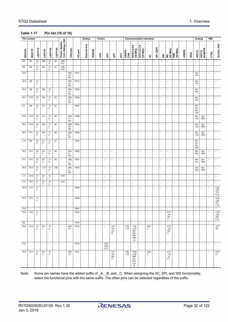
R01DS0262EU0130 Rev.1.30 Page 32 of 122Jan 3, 2018
S7G2 Datasheet 1. Overview
Note: Some pin names have the added suffix of _A, _B, and _C. When assigning the IIC, SPI, and SSI functionality, select the functional pins with the same suffix. The other pins can be selected regardless of the suffix.
P9 P9 157
M8 129
90 VREFL0
- - - - - - - - - - - - - - - - - - - - - -
R9 R9 158
N8 130
91 VREFH0
- - - - - - - - - - - - - - - - - - - - - -
N10 - - - - - - IRQ15-DS
P011 - - - - - - - - - - - - - - - - AN104
- - -
M10 M8 159
- - - - IRQ14-DS
P010 - - - - - - - - - - - - - - - - AN103
- - -
R10 M9 160
M9 131
- - IRQ13-DS
P009 - - - - - - - - - - - - - - - - AN004
- - -
N11 P10 161
N9 132
92 - IRQ12-DS
P008 - - - - - - - - - - - - - - - - AN003
- - -
L9 M6 162
K7 133
93 - - P007 - - - - - - - - - - - - - - - - PGAVSS100
- - -
P10 N10 163
L9 134
94 - IRQ11-DS
P006 - - - - - - - - - - - - - - - - AN102
IVCMP2
- -
R11 R10 164
K8 135
95 - IRQ10-DS
P005 - - - - - - - - - - - - - - - - AN101
IVCMP2
- -
M11 P11 165
K9 136
96 - IRQ9-DS
P004 - - - - - - - - - - - - - - - - AN100
IVCMP2
- -
L10 M5 166
K10
137
97 - - P003 - - - - - - - - - - - - - - - - PGAVSS000
- - -
N12 R11 167
M10
138
98 - IRQ8-DS
P002 - - - - - - - - - - - - - - - - AN002
IVCMP2
- -
P11 N11 168
N10
139
99 - IRQ7-DS
P001 - - - - - - - - - - - - - - - - AN001
IVCMP2
- -
R12 R12 169
L10 140
100 - IRQ6-DS
P000 - - - - - - - - - - - - - - - - AN000
IVCMP2
- -
L11 M10 170
N11
141
- VSS - - - - - - - - - - - - - - - - - - - - - -
L12 M11 171
N12
142
- VCC - - - - - - - - - - - - - - - - - - - - - -
M12 P12 172
- - - - - P806 - - - - - - - - - - - - - - - - - - - LCD_EXTCLK_B
R13 R13 173
- - - - - P805 - - - - - - - - - - - - - - - - - - - LCD_DATA17_B
P12 - - - - - - - P807 - - - - - - - - - - - - - - - - - - - -
P13 N12 174
- - - - - P513 - - - - - - - - - - - - ET1_ETXD3
- - - - - - LCD_DATA16_B
K9 - - - - - - - P515 - - - - - - - - - - - - - - - - - - - -
R14 R14 175
M11
143
- - IRQ14
P512 - - - - GTIOC0A_B
- CTX1_B
TXD4_B/MOSI4_B/SDA4_B
- SCL2
- - ET1_ETXD2
- - - - - - VSYNC
P14 - - - - - - P514 - - - GTETRGB_C
- - - - - - - - - - - - - - - -
R15 P13 176
M12
144
- - IRQ15
P511 - - - - GTIOC0B_B
- CRX1_B
RXD4_B/MISO4_B/SCL4_B
- SDA2
- - ET1_TX_ER
- - - - - - PCKO
Table 1.17 Pin list (10 of 10)
Pin number
Po
wer
, S
yst
em,
CL
K, D
ebu
g, C
AC
Inte
rru
pt
I/O
po
rt
Extbus Timers Communication interfaces Analog HMI
BG
A2
24
BG
A1
76
LQ
FP
176
LG
A14
5
LQ
FP
144
LQ
FP
100
Ext
ern
al b
us
SD
RA
M
AG
T
GP
T
GP
T
RT
C
US
BF
S,
CA
N
SC
I0,2
,4,6
,8(3
0 M
Hz)
SC
I1,3
,5,7
,9(3
0 M
Hz)
IIC
SP
I, Q
SP
I
SS
I
MII
(25
MH
z)
RM
II(5
0 M
Hz)
US
BH
S
SD
HI
AD
C12
DA
C12
,A
CM
PH
S
CT
SU
GL
CD
C,
PD
C
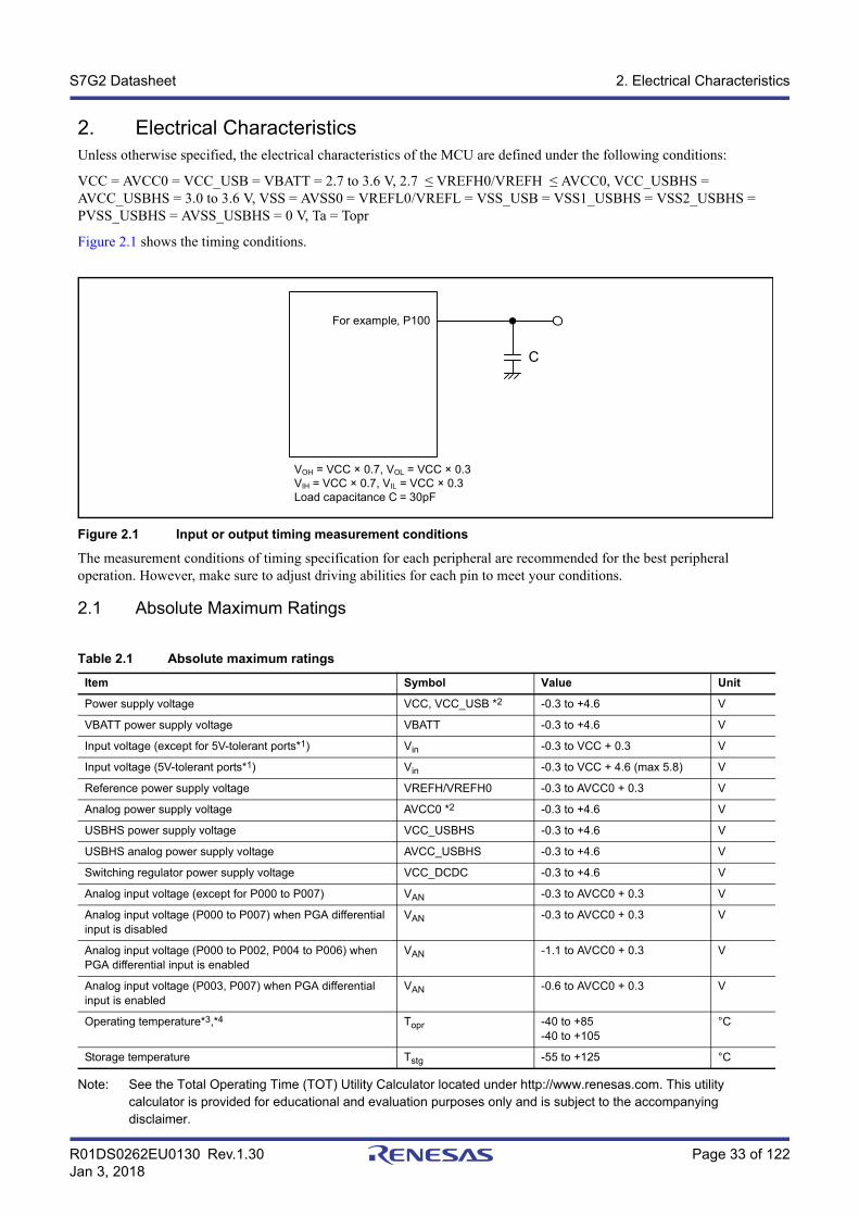
R01DS0262EU0130 Rev.1.30 Page 33 of 122Jan 3, 2018
S7G2 Datasheet 2. Electrical Characteristics
2. Electrical CharacteristicsUnless otherwise specified, the electrical characteristics of the MCU are defined under the following conditions:
VCC = AVCC0 = VCC_USB = VBATT = 2.7 to 3.6 V, 2.7 ≤ VREFH0/VREFH ≤ AVCC0, VCC_USBHS = AVCC_USBHS = 3.0 to 3.6 V, VSS = AVSS0 = VREFL0/VREFL = VSS_USB = VSS1_USBHS = VSS2_USBHS = PVSS_USBHS = AVSS_USBHS = 0 V, Ta = Topr
Figure 2.1 shows the timing conditions.
Figure 2.1 Input or output timing measurement conditions
The measurement conditions of timing specification for each peripheral are recommended for the best peripheral operation. However, make sure to adjust driving abilities for each pin to meet your conditions.
2.1 Absolute Maximum Ratings
Note: See the Total Operating Time (TOT) Utility Calculator located under http://www.renesas.com. This utility calculator is provided for educational and evaluation purposes only and is subject to the accompanying disclaimer.
Table 2.1 Absolute maximum ratings
Item Symbol Value Unit
Power supply voltage VCC, VCC_USB *2 -0.3 to +4.6 V
VBATT power supply voltage VBATT -0.3 to +4.6 V
Input voltage (except for 5V-tolerant ports*1) Vin -0.3 to VCC + 0.3 V
Input voltage (5V-tolerant ports*1) Vin -0.3 to VCC + 4.6 (max 5.8) V
Reference power supply voltage VREFH/VREFH0 -0.3 to AVCC0 + 0.3 V
Analog power supply voltage AVCC0 *2 -0.3 to +4.6 V
USBHS power supply voltage VCC_USBHS -0.3 to +4.6 V
USBHS analog power supply voltage AVCC_USBHS -0.3 to +4.6 V
Switching regulator power supply voltage VCC_DCDC -0.3 to +4.6 V
Analog input voltage (except for P000 to P007) VAN -0.3 to AVCC0 + 0.3 V
Analog input voltage (P000 to P007) when PGA differential input is disabled
VAN -0.3 to AVCC0 + 0.3 V
Analog input voltage (P000 to P002, P004 to P006) when PGA differential input is enabled
VAN -1.1 to AVCC0 + 0.3 V
Analog input voltage (P003, P007) when PGA differential input is enabled
VAN -0.6 to AVCC0 + 0.3 V
Operating temperature*3,*4 Topr -40 to +85-40 to +105
°C
Storage temperature Tstg -55 to +125 °C
For example, P100
C
VOH = VCC × 0.7, VOL = VCC × 0.3VIH = VCC × 0.7, VIL = VCC × 0.3Load capacitance C = 30pF
R01DS0262EU0130 Rev.1.30 Page 34 of 122Jan 3, 2018
S7G2 Datasheet 2. Electrical Characteristics
Note 1. Ports P205, P206, P400, P401, P407 to P415, P511, P512, P708 to P713, and PB01 are 5V-tolerant.Note 2. Connect AVCC0 and VCC_USB to VCC.Note 3. See section 2.2.1, Tj/Ta Definition.Note 4. The upper limit of operating temperature is 85°C or 105°C, depending on the product. For details, see section
1.3, Part Numbering.Caution: Permanent damage to the MCU might result if absolute maximum ratings are exceeded.
2.2 DC Characteristics
2.2.1 Tj/Ta Definition
Note: Make sure that Tj = Ta + θja × total power consumption (W), where total power consumption = (VCC – VOH) ×
ΣIOH + VOL × ΣIOL + ICCmax × VCC.
Note 1. The upper limit of operating temperature is 85°C or 105°C depending on the product. For details, see section 1.3, Part Numbering. If the part number shows the operation temperature as 85°C, then the maximum value of Tj is 105°C, otherwise it is 125°C.
Table 2.2 Recommended operating conditions
Item Symbol Value Min Typ Max Unit
Power supply voltages VCC When USB/SDRAM is not used 2.7 - 3.6 V
When USB/SDRAM is used 3.0 - 3.6 V
VSS - 0 - V
USB power supply voltages VCC_USB,VCC_USBHS
- VCC - V
VSS_USB,AVSS_USBHS,PVSS_USBHS,VSS1_USBHS,VSS2_USBHS
- 0 - V
Switching regulator power supply voltage
VCC_DCDC When switching regulator is used
- VCC - V
When switching regulator is not used
- 0 - V
VBATT power supply voltage VBATT 2.0 3.6 V
Analog power supply voltages AVCC0 - VCC - V
AVSS0 - 0 - V
Table 2.3 DC characteristicsConditions: Products with operating temperature (Ta) –40 to +105°C
Item Symbol Typ Max Unit Test conditions
Permissible junction temperature Tj - 125 °C High-speed modeLow-speed modeSubosc-speed mode
105*1
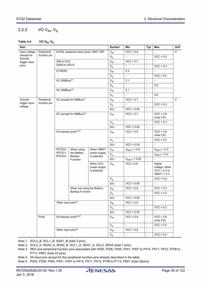
R01DS0262EU0130 Rev.1.30 Page 35 of 122Jan 3, 2018
S7G2 Datasheet 2. Electrical Characteristics
2.2.2 I/O VIH, VIL
Note 1. SCL0_B, SCL1_B, SDA1_B (total 3 pins).Note 2. SCL0_A, SDA0_A, SDA0_B, SCL1_A, SDA1_A, SCL2, SDA2 (total 7 pins).Note 3. RES and peripheral function pins associated with P205, P206, P400, P401, P407 to P415, P511, P512, P708 to
P713, PB01 (total 23 pins).Note 4. All input pins except for the peripheral function pins already described in the table.Note 5. P205, P206, P400, P401, P407 to P415, P511, P512, P708 to P713, PB01 (total 22pins).
Table 2.4 I/O VIH, VIL
Item Symbol Min Typ Max Unit
Input voltage (except for Schmitt trigger input pins)
Peripheral function pin
EXTAL (external clock input), WAIT, SPI VIH VCC × 0.8 - - V
VIL - - VCC × 0.2
D00 to D15,DQ00 to DQ15
VIH VCC × 0.7 - -
VIL - - VCC × 0.3
ETHERC VIH 2.3 - -
VIL - - VCC × 0.2
IIC (SMBus)*1 VIH 2.1 - -
VIL - - 0.8
IIC (SMBus)*2 VIH 2.1 - -
VIL - - 0.8
Schmitt trigger input voltage
Peripheral function pin
IIC (except for SMBus)*1 VIH VCC × 0.7 - - V
VIL - - VCC × 0.3
∆VT VCC × 0.05 - -
IIC (except for SMBus)*2 VIH VCC × 0.7 - VCC + 3.6 (max 5.8)
VIL - - VCC × 0.3
∆VT VCC × 0.05 - -
5V-tolerant ports*3*7 VIH VCC × 0.8 - VCC + 3.6 (max 5.8)
VIL - - VCC × 0.2
∆VT VCC × 0.05 - -
RTCIC0, RTCIC1, RTCIC2
When using the Battery Backup Function
When VBATT power supply is selected
VIH VBATT × 0.8 - VBATT + 0.3
VIL - - VBATT × 0.2
∆VT VBATT × 0.05 - -
When VCC power supply is selected
VIH VCC x 0.8 - Higher voltage, either VCC + 0.3 or VBATT + 0.3
VIL - - VCC × 0.2
∆VT VCC × 0.05 - -
When not using the Battery Backup Function
VIH VCC × 0.8 - VCC + 0.3
VIL - - VCC × 0.2
∆VT VCC × 0.05 - -
Other input pins*4 VIH VCC × 0.8 - -
VIL - - VCC × 0.2
∆VT VCC × 0.05 - -
Ports 5V-tolerant ports*5*7 VIH VCC × 0.8 - VCC + 3.6 (max 5.8)
VIL - - VCC × 0.2
Other input pins*6 VIH VCC × 0.8 - -
VIL - - VCC × 0.2
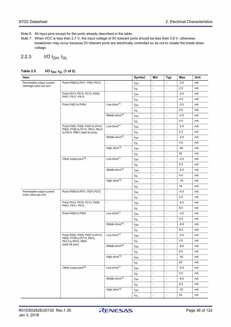
R01DS0262EU0130 Rev.1.30 Page 36 of 122Jan 3, 2018
S7G2 Datasheet 2. Electrical Characteristics
Note 6. All input pins except for the ports already described in the table.Note 7. When VCC is less than 2.7 V, the input voltage of 5V-tolerant ports should be less than 3.6 V, otherwise
breakdown may occur because 5V-tolerant ports are electrically controlled so as not to violate the break down voltage.
2.2.3 I/O IOH, IOL
Table 2.5 I/O IOH, IOL (1 of 2)
Item Symbol Min Typ Max Unit
Permissible output current (average value per pin)
Ports P008 to P011, P201,P212 - IOH - -- -2.0 mA
IOL - - 2.0 mA
Ports P014, P015, P213, P400, P401, P511, P512
- IOH - - -4.0 mA
IOL - - 4.0 mA
Ports P402 to P404 Low drive*1 IOH - - -2.0 mA
IOL - - 2.0 mA
Middle drive*2 IOH - - -4.0 mA
IOL - - 4.0 mA
Ports P205, P206, P407 to P415, P602, P708 to P713, P813, PA12 to PA15, PB01 (total 24 pins)
Low drive*1 IOH - - -2.0 mA
IOL - - 2.0 mA
Middle drive*2 IOH - - -4.0 mA
IOL - - 4.0 mA
High drive*3 IOH - - -20 mA
IOL - - 20 mA
Other output pins*4 Low drive*1 IOH - - -2.0 mA
IOL - - 2.0 mA
Middle drive*2 IOH - - -4.0 mA
IOL - - 4.0 mA
High drive*3 IOH - - -16 mA
IOL - - 16 mA
Permissible output current (max value per pin)
Ports P008 to P011, P201,P212 - IOH - - -4.0 mA
IOL - - 4.0 mA
Ports P014, P015, P213, P400, P401, P511, P512
- IOH - - -8.0 mA
IOL - - 8.0 mA
Ports P402 to P404 Low drive*1 IOH - - -4.0 mA
IOL - - 4.0 mA
Middle drive*2 IOH - - -8.0 mA
IOL - - 8.0 mA
Ports P205, P206, P407 to P415, P602, P708 to P713, P813, PA12 to PA15, PB01(total 24 pins)
Low drive*1 IOH - - -4.0 mA
IOL - - 4.0 mA
Middle drive*2 IOH - - -8.0 mA
IOL - - 8.0 mA
High drive*3 IOH - - -40 mA
IOL - - 40 mA
Other output pins*4 Low drive*1 IOH - - -4.0 mA
IOL - - 4.0 mA
Middle drive*2 IOH - - -8.0 mA
IOL - - 8.0 mA
High drive*3 IOH - - -32 mA
IOL - - 32 mA
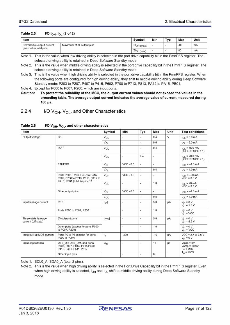
R01DS0262EU0130 Rev.1.30 Page 37 of 122Jan 3, 2018
S7G2 Datasheet 2. Electrical Characteristics
Note 1. This is the value when low driving ability is selected in the port drive capability bit in the PmnPFS register. The selected driving ability is retained in Deep Software Standby mode.
Note 2. This is the value when middle driving ability is selected in the port drive capability bit in the PmnPFS register. The selected driving ability is retained in Deep Software Standby mode.
Note 3. This is the value when high driving ability is selected in the port drive capability bit in the PmnPFS register. When the following ports are configured for high driving ability, they shift to middle driving ability during Deep Software Standby mode: P203 to P207, P407 to P415, P602, P708 to P713, P813, PA12 to PA15, PB01.
Note 4. Except for P000 to P007, P200, which are input ports.Caution: To protect the reliability of the MCU, the output current values should not exceed the values in the
preceding table. The average output current indicates the average value of current measured during 100 μs.
2.2.4 I/O VOH, VOL, and Other Characteristics
Note 1. SCL0_A, SDA0_A (total 2 pins).Note 2. This is the value when high driving ability is selected in the Port Drive Capability bit in the PmnPFS register. Even
when high driving ability is selected, IOH and IOL shift to middle driving ability during Deep Software Standby
mode.
Permissible output current (max value total pins)
Maximum of all output pins ΣIOH (max) - - -80 mA
ΣIOL (max) - - 80 mA
Table 2.6 I/O VOH, VOL, and other characteristics
Item Symbol Min Typ Max Unit Test conditions
Output voltage IIC VOL - - 0.4 V IOL = 3.0 mA
VOL - - 0.6 IOL = 6.0 mA
IIC*1 VOL - - 0.4 IOL = 15.0 mA(ICFER.FMPE = 1)
VOL - 0.4 - IOL = 20.0 mA(ICFER.FMPE = 1)
ETHERC VOH VCC - 0.5 - - IOH = –1.0 mA
VOL - - 0.4 IOL = 1.0 mA
Ports P205, P206, P407 to P415, P602, P708 to P713, P813, PA12 to PA15, PB01 (total 24 pins)*2
VOH VCC - 1.0 - - IOH = –20 mAVCC = 3.3 V
VOL - - 1.0 IOL = 20 mAVCC = 3.3 V
Other output pins VOH VCC - 0.5 - - IOH = –1.0 mA
VOL - - 0.5 IOL = 1.0 mA
Input leakage current RES |Iin| - - 5.0 μA Vin = 0 VVin = 5.5 V
Ports P000 to P007, P200 - - 1.0 Vin = 0 VVin = VCC
Three-state leakage current (off state)
5V-tolerant ports |ITSI| - - 5.0 μA Vin = 0 VVin = 5.5 V
Other ports (except for ports P000 to P007, P200)
- - 1.0 Vin = 0 VVin = VCC
Input pull-up MOS current Ports P0 to PB (except for ports P000 to P007)
Ip -300 - -10 μA VCC = 2.7 to 3.6 VVin = 0 V
Input capacitance USB_DP, USB_DM, and ports P003, P007, P014, P015,P400, P415, P401, P511, P512
Cin - - 16 pF Vbias = 0VVamp = 20mVf = 1 MHzTa = 25°C
Other input pins - - 8
Table 2.5 I/O IOH, IOL (2 of 2)
Item Symbol Min Typ Max Unit
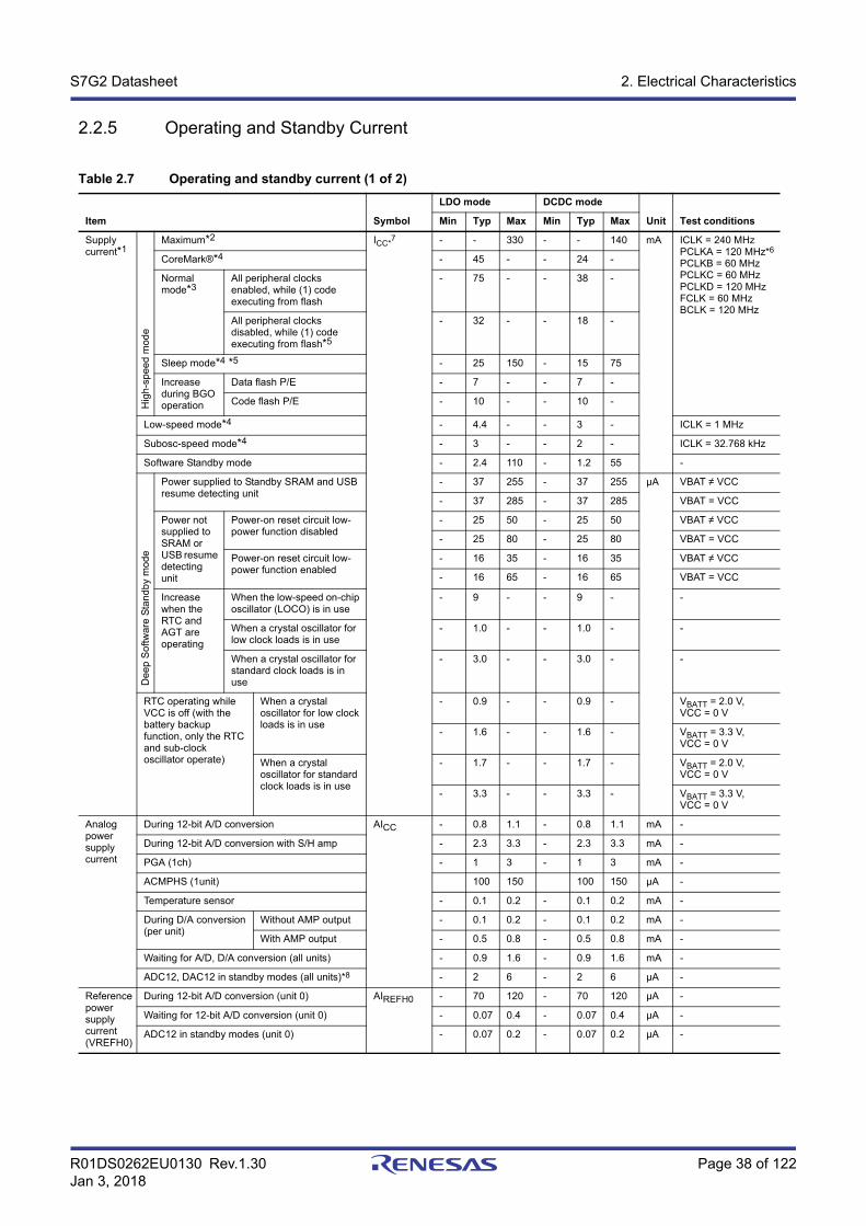
R01DS0262EU0130 Rev.1.30 Page 38 of 122Jan 3, 2018
S7G2 Datasheet 2. Electrical Characteristics
2.2.5 Operating and Standby Current
Table 2.7 Operating and standby current (1 of 2)
Item Symbol
LDO mode DCDC mode
Unit Test conditionsMin Typ Max Min Typ Max
Supply current*1
Hig
h-s
pe
ed m
ode
Maximum*2 ICC*7 - - 330 - - 140 mA ICLK = 240 MHz
PCLKA = 120 MHz*6
PCLKB = 60 MHzPCLKC = 60 MHzPCLKD = 120 MHzFCLK = 60 MHzBCLK = 120 MHz
CoreMark®*4 - 45 - - 24 -
Normal mode*3
All peripheral clocks enabled, while (1) code executing from flash
- 75 - - 38 -
All peripheral clocks disabled, while (1) code executing from flash*5
- 32 - - 18 -
Sleep mode*4 *5 - 25 150 - 15 75
Increase during BGO operation
Data flash P/E - 7 - - 7 -
Code flash P/E - 10 - - 10 -
Low-speed mode*4 - 4.4 - - 3 - ICLK = 1 MHz
Subosc-speed mode*4 - 3 - - 2 - ICLK = 32.768 kHz
Software Standby mode - 2.4 110 - 1.2 55 -
Dee
p S
oftw
are
Sta
nd
by
mo
de
Power supplied to Standby SRAM and USB resume detecting unit
- 37 255 - 37 255 μA VBAT ≠ VCC
- 37 285 - 37 285 VBAT = VCC
Power not supplied to SRAM or USB resume detecting unit
Power-on reset circuit low-power function disabled
- 25 50 - 25 50 VBAT ≠ VCC
- 25 80 - 25 80 VBAT = VCC
Power-on reset circuit low-power function enabled
- 16 35 - 16 35 VBAT ≠ VCC
- 16 65 - 16 65 VBAT = VCC
Increase when the RTC and AGT are operating
When the low-speed on-chip oscillator (LOCO) is in use
- 9 - - 9 - -
When a crystal oscillator for low clock loads is in use
- 1.0 - - 1.0 - -
When a crystal oscillator for standard clock loads is in use
- 3.0 - - 3.0 - -
RTC operating while VCC is off (with the battery backup function, only the RTC and sub-clock oscillator operate)
When a crystal oscillator for low clock loads is in use
- 0.9 - - 0.9 - VBATT = 2.0 V, VCC = 0 V
- 1.6 - - 1.6 - VBATT = 3.3 V, VCC = 0 V
When a crystal oscillator for standard clock loads is in use
- 1.7 - - 1.7 - VBATT = 2.0 V, VCC = 0 V
- 3.3 - - 3.3 - VBATT = 3.3 V, VCC = 0 V
Analog power supply current
During 12-bit A/D conversion AICC - 0.8 1.1 - 0.8 1.1 mA -
During 12-bit A/D conversion with S/H amp - 2.3 3.3 - 2.3 3.3 mA -
PGA (1ch) - 1 3 - 1 3 mA -
ACMPHS (1unit) 100 150 100 150 µA -
Temperature sensor - 0.1 0.2 - 0.1 0.2 mA -
During D/A conversion (per unit)
Without AMP output - 0.1 0.2 - 0.1 0.2 mA -
With AMP output - 0.5 0.8 - 0.5 0.8 mA -
Waiting for A/D, D/A conversion (all units) - 0.9 1.6 - 0.9 1.6 mA -
ADC12, DAC12 in standby modes (all units)*8 - 2 6 - 2 6 µA -
Reference power supply current (VREFH0)
During 12-bit A/D conversion (unit 0) AIREFH0 - 70 120 - 70 120 μA -
Waiting for 12-bit A/D conversion (unit 0) - 0.07 0.4 - 0.07 0.4 μA -
ADC12 in standby modes (unit 0) - 0.07 0.2 - 0.07 0.2 µA -
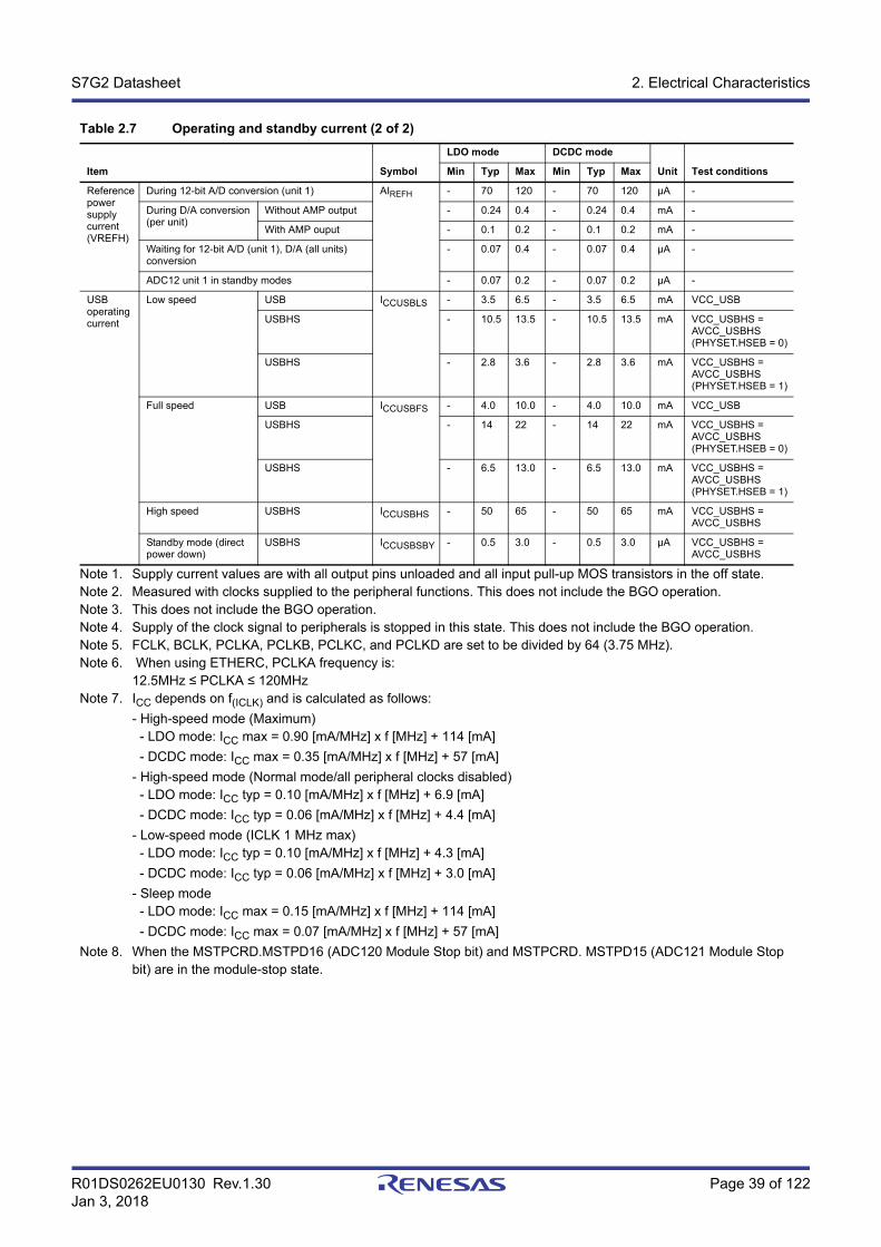
R01DS0262EU0130 Rev.1.30 Page 39 of 122Jan 3, 2018
S7G2 Datasheet 2. Electrical Characteristics
Note 1. Supply current values are with all output pins unloaded and all input pull-up MOS transistors in the off state.Note 2. Measured with clocks supplied to the peripheral functions. This does not include the BGO operation.Note 3. This does not include the BGO operation.Note 4. Supply of the clock signal to peripherals is stopped in this state. This does not include the BGO operation.Note 5. FCLK, BCLK, PCLKA, PCLKB, PCLKC, and PCLKD are set to be divided by 64 (3.75 MHz).Note 6. When using ETHERC, PCLKA frequency is:
12.5MHz ≤ PCLKA ≤ 120MHzNote 7. ICC depends on f(ICLK) and is calculated as follows:
- High-speed mode (Maximum)- LDO mode: ICC max = 0.90 [mA/MHz] x f [MHz] + 114 [mA]
- DCDC mode: ICC max = 0.35 [mA/MHz] x f [MHz] + 57 [mA]
- High-speed mode (Normal mode/all peripheral clocks disabled)- LDO mode: ICC typ = 0.10 [mA/MHz] x f [MHz] + 6.9 [mA]
- DCDC mode: ICC typ = 0.06 [mA/MHz] x f [MHz] + 4.4 [mA]
- Low-speed mode (ICLK 1 MHz max)- LDO mode: ICC typ = 0.10 [mA/MHz] x f [MHz] + 4.3 [mA]
- DCDC mode: ICC typ = 0.06 [mA/MHz] x f [MHz] + 3.0 [mA]
- Sleep mode - LDO mode: ICC max = 0.15 [mA/MHz] x f [MHz] + 114 [mA]
- DCDC mode: ICC max = 0.07 [mA/MHz] x f [MHz] + 57 [mA]
Note 8. When the MSTPCRD.MSTPD16 (ADC120 Module Stop bit) and MSTPCRD. MSTPD15 (ADC121 Module Stop bit) are in the module-stop state.
Reference power supply current (VREFH)
During 12-bit A/D conversion (unit 1) AIREFH - 70 120 - 70 120 µA -
During D/A conversion (per unit)
Without AMP output - 0.24 0.4 - 0.24 0.4 mA -
With AMP ouput - 0.1 0.2 - 0.1 0.2 mA -
Waiting for 12-bit A/D (unit 1), D/A (all units) conversion
- 0.07 0.4 - 0.07 0.4 µA -
ADC12 unit 1 in standby modes - 0.07 0.2 - 0.07 0.2 µA -
USB operating current
Low speed USB ICCUSBLS - 3.5 6.5 - 3.5 6.5 mA VCC_USB
USBHS - 10.5 13.5 - 10.5 13.5 mA VCC_USBHS = AVCC_USBHS (PHYSET.HSEB = 0)
USBHS - 2.8 3.6 - 2.8 3.6 mA VCC_USBHS = AVCC_USBHS (PHYSET.HSEB = 1)
Full speed USB ICCUSBFS - 4.0 10.0 - 4.0 10.0 mA VCC_USB
USBHS - 14 22 - 14 22 mA VCC_USBHS = AVCC_USBHS (PHYSET.HSEB = 0)
USBHS - 6.5 13.0 - 6.5 13.0 mA VCC_USBHS = AVCC_USBHS (PHYSET.HSEB = 1)
High speed USBHS ICCUSBHS - 50 65 - 50 65 mA VCC_USBHS = AVCC_USBHS
Standby mode (direct power down)
USBHS ICCUSBSBY - 0.5 3.0 - 0.5 3.0 μA VCC_USBHS = AVCC_USBHS
Table 2.7 Operating and standby current (2 of 2)
Item Symbol
LDO mode DCDC mode
Unit Test conditionsMin Typ Max Min Typ Max
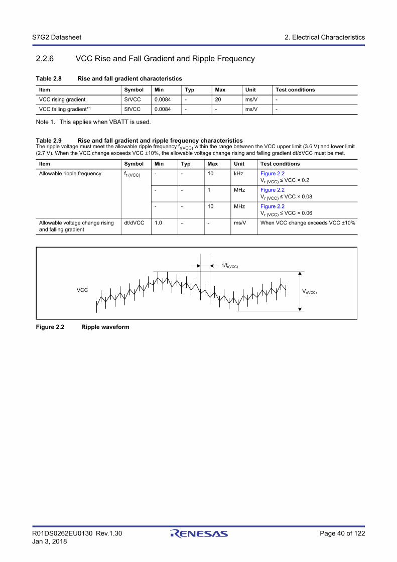
R01DS0262EU0130 Rev.1.30 Page 40 of 122Jan 3, 2018
S7G2 Datasheet 2. Electrical Characteristics
2.2.6 VCC Rise and Fall Gradient and Ripple Frequency
Note 1. This applies when VBATT is used.
Figure 2.2 Ripple waveform
Table 2.8 Rise and fall gradient characteristics
Item Symbol Min Typ Max Unit Test conditions
VCC rising gradient SrVCC 0.0084 - 20 ms/V -
VCC falling gradient*1 SfVCC 0.0084 - - ms/V -
Table 2.9 Rise and fall gradient and ripple frequency characteristicsThe ripple voltage must meet the allowable ripple frequency fr(VCC) within the range between the VCC upper limit (3.6 V) and lower limit (2.7 V). When the VCC change exceeds VCC ±10%, the allowable voltage change rising and falling gradient dt/dVCC must be met.
Item Symbol Min Typ Max Unit Test conditions
Allowable ripple frequency fr (VCC) - - 10 kHz Figure 2.2Vr (VCC) ≤ VCC × 0.2
- - 1 MHz Figure 2.2Vr (VCC) ≤ VCC × 0.08
- - 10 MHz Figure 2.2Vr (VCC) ≤ VCC × 0.06
Allowable voltage change rising and falling gradient
dt/dVCC 1.0 - - ms/V When VCC change exceeds VCC ±10%
Vr(VCC)VCC
1/fr(VCC)
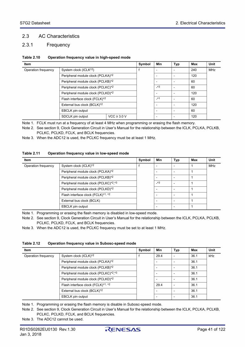
R01DS0262EU0130 Rev.1.30 Page 41 of 122Jan 3, 2018
S7G2 Datasheet 2. Electrical Characteristics
2.3 AC Characteristics
2.3.1 Frequency
Note 1. FCLK must run at a frequency of at least 4 MHz when programming or erasing the flash memory.Note 2. See section 9, Clock Generation Circuit in User’s Manual for the relationship between the ICLK, PCLKA, PCLKB,
PCLKC, PCLKD, FCLK, and BCLK frequencies.Note 3. When the ADC12 is used, the PCLKC frequency must be at least 1 MHz.
Note 1. Programming or erasing the flash memory is disabled in low-speed mode.Note 2. See section 9, Clock Generation Circuit in User’s Manual for the relationship between the ICLK, PCLKA, PCLKB,
PCLKC, PCLKD, FCLK, and BCLK frequencies.Note 3. When the ADC12 is used, the PCLKC frequency must be set to at least 1 MHz.
Note 1. Programming or erasing the flash memory is disable in Subosc-speed mode.Note 2. See section 9, Clock Generation Circuit in User’s Manual for the relationship between the ICLK, PCLKA, PCLKB,
PCLKC, PCLKD, FCLK, and BCLK frequencies.Note 3. The ADC12 cannot be used.
Table 2.10 Operation frequency value in high-speed mode
Item Symbol Min Typ Max Unit
Operation frequency System clock (ICLK*2) f - - 240 MHz
Peripheral module clock (PCLKA)*2 - - 120
Peripheral module clock (PCLKB)*2 - - 60
Peripheral module clock (PCLKC)*2 -*3 - 60
Peripheral module clock (PCLKD)*2 - - 120
Flash interface clock (FCLK)*2 -*1 - 60
External bus clock (BCLK)*2 - - 120
EBCLK pin output - - 60
SDCLK pin output VCC ≥ 3.0 V - - 120
Table 2.11 Operation frequency value in low-speed mode
Item Symbol Min Typ Max Unit
Operation frequency System clock (ICLK)*2 f - - 1 MHz
Peripheral module clock (PCLKA)*2 - - 1
Peripheral module clock (PCLKB)*2 - - 1
Peripheral module clock (PCLKC)*2,*3 -*3 - 1
Peripheral module clock (PCLKD)*2 - - 1
Flash interface clock (FCLK)*1, *2 - - 1
External bus clock (BCLK) - - 1
EBCLK pin output - - 1
Table 2.12 Operation frequency value in Subosc-speed mode
Item Symbol Min Typ Max Unit
Operation frequency System clock (ICLK)*2 f 29.4 - 36.1 kHz
Peripheral module clock (PCLKA)*2 - - 36.1
Peripheral module clock (PCLKB)*2 - - 36.1
Peripheral module clock (PCLKC)*2,*3 - - 36.1
Peripheral module clock (PCLKD)*2 - - 36.1
Flash interface clock (FCLK)*1, *2 29.4 - 36.1
External bus clock (BCLK)*2 - - 36.1
EBCLK pin output - - 36.1
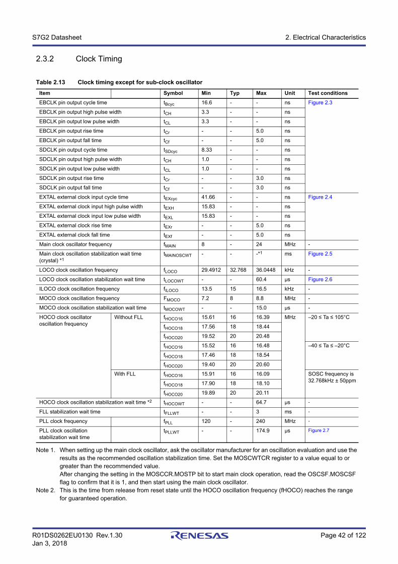
R01DS0262EU0130 Rev.1.30 Page 42 of 122Jan 3, 2018
S7G2 Datasheet 2. Electrical Characteristics
2.3.2 Clock Timing
Note 1. When setting up the main clock oscillator, ask the oscillator manufacturer for an oscillation evaluation and use the results as the recommended oscillation stabilization time. Set the MOSCWTCR register to a value equal to or greater than the recommended value.After changing the setting in the MOSCCR.MOSTP bit to start main clock operation, read the OSCSF.MOSCSF flag to confirm that it is 1, and then start using the main clock oscillator.
Note 2. This is the time from release from reset state until the HOCO oscillation frequency (fHOCO) reaches the range for guaranteed operation.
Table 2.13 Clock timing except for sub-clock oscillator
Item Symbol Min Typ Max Unit Test conditions
EBCLK pin output cycle time tBcyc 16.6 - - ns Figure 2.3
EBCLK pin output high pulse width tCH 3.3 - - ns
EBCLK pin output low pulse width tCL 3.3 - - ns
EBCLK pin output rise time tCr - - 5.0 ns
EBCLK pin output fall time tCf - - 5.0 ns
SDCLK pin output cycle time tSDcyc 8.33 - - ns
SDCLK pin output high pulse width tCH 1.0 - - ns
SDCLK pin output low pulse width tCL 1.0 - - ns
SDCLK pin output rise time tCr - - 3.0 ns
SDCLK pin output fall time tCf - - 3.0 ns
EXTAL external clock input cycle time tEXcyc 41.66 - - ns Figure 2.4
EXTAL external clock input high pulse width tEXH 15.83 - - ns
EXTAL external clock input low pulse width tEXL 15.83 - - ns
EXTAL external clock rise time tEXr - - 5.0 ns
EXTAL external clock fall time tEXf - - 5.0 ns
Main clock oscillator frequency fMAIN 8 - 24 MHz -
Main clock oscillation stabilization wait time (crystal) *1
tMAINOSCWT - - -*1 ms Figure 2.5
LOCO clock oscillation frequency fLOCO 29.4912 32.768 36.0448 kHz -
LOCO clock oscillation stabilization wait time tLOCOWT - - 60.4 μs Figure 2.6
ILOCO clock oscillation frequency fILOCO 13.5 15 16.5 kHz -
MOCO clock oscillation frequency FMOCO 7.2 8 8.8 MHz -
MOCO clock oscillation stabilization wait time tMOCOWT - - 15.0 μs -
HOCO clock oscillator oscillation frequency
Without FLL fHOCO16 15.61 16 16.39 MHz –20 ≤ Ta ≤ 105°C
fHOCO18 17.56 18 18.44
fHOCO20 19.52 20 20.48
fHOCO16 15.52 16 16.48 –40 ≤ Ta ≤ –20°C
fHOCO18 17.46 18 18.54
fHOCO20 19.40 20 20.60
With FLL fHOCO16 15.91 16 16.09 SOSC frequency is 32.768kHz ± 50ppmfHOCO18 17.90 18 18.10
fHOCO20 19.89 20 20.11
HOCO clock oscillation stabilization wait time *2 tHOCOWT - - 64.7 μs -
FLL stabilization wait time tFLLWT - - 3 ms -
PLL clock frequency fPLL 120 - 240 MHz -
PLL clock oscillation stabilization wait time
tPLLWT - - 174.9 μs Figure 2.7
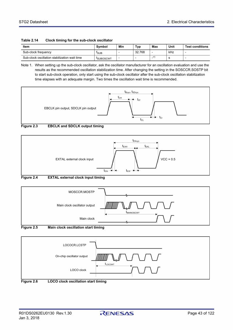
R01DS0262EU0130 Rev.1.30 Page 43 of 122Jan 3, 2018
S7G2 Datasheet 2. Electrical Characteristics
Note 1. When setting up the sub-clock oscillator, ask the oscillator manufacturer for an oscillation evaluation and use the results as the recommended oscillation stabilization time. After changing the setting in the SOSCCR.SOSTP bit to start sub-clock operation, only start using the sub-clock oscillator after the sub-clock oscillation stabilization time elapses with an adequate margin. Two times the oscillation wait time is recommended.
Figure 2.3 EBCLK and SDCLK output timing
Figure 2.4 EXTAL external clock input timing
Figure 2.5 Main clock oscillation start timing
Figure 2.6 LOCO clock oscillation start timing
Table 2.14 Clock timing for the sub-clock oscillator
Item Symbol Min Typ Max Unit Test conditions
Sub-clock frequency fSUB - 32.768 - kHz -
Sub-clock oscillation stabilization wait time tSUBOSCWT - - -*1 s -
tCftCH
tBcyc, tSDcyc
tCrtCL
EBCLK pin output, SDCLK pin output
tEXH
tEXcyc
EXTAL external clock input VCC × 0.5
tEXL
tEXr tEXf
Main clock oscillator output
MOSCCR.MOSTP
Main clock
tMAINOSCWT
LOCO clock
LOCOCR.LCSTP
tLOCOWT
On-chip oscillator output
R01DS0262EU0130 Rev.1.30 Page 44 of 122Jan 3, 2018
S7G2 Datasheet 2. Electrical Characteristics
Figure 2.7 PLL clock oscillation start timing
Note: Only operate the PLL is operated after main clock oscillation has stabilized.
2.3.3 Reset Timing
Figure 2.8 Power-on reset timing
Figure 2.9 Reset input timing
Table 2.15 Reset timing
Item Symbol Min Typ Max UnitTest conditions
RES pulse width Power-on LDO mode tRESWP 1 - - ms Figure 2.8
DCDC mode 1.5 - - ms
Deep Software Standby mode tRESWD 0.6 - - ms Figure 2.9
Software Standby mode, Subosc-speed mode
tRESWS 0.3 - - ms
All other tRESW 200 - - μs
Wait time after RES cancellation tRESWT - - 33.4 μs Figure 2.8
Wait time after internal reset cancellation(IWDT reset, WDT reset, software reset, SRAM parity error reset, SRAM DED error reset, bus master MPU error reset, bus slave MPU error reset, stack pointer error reset)
tRESW2 - - 390 μs -
PLLCR.PLLSTP
OSCSF.PLLSF
PLL clock
tPLLWT
PLL circuit output
VCC
RES
Internal reset signal(active-low)
tRESWP
tRESWT
RES
Internal reset signal(active-low)
tRESWD, tRESWS, tRESW
tRESWT
R01DS0262EU0130 Rev.1.30 Page 45 of 122Jan 3, 2018
S7G2 Datasheet 2. Electrical Characteristics
2.3.4 Wakeup Timing and Duration
Note 1. The recovery time is determined by the system clock source. When multiple oscillators are active, the recovery time can be determined with the following equation:Total recovery time = recovery time for an oscillator as the system clock source + the longest oscillation stabilization time of any oscillators requiring longer stabilization times than the system clock source + 2 LOCO cycles (when LOCO is operating) + 3 SOSC cycles (when Subosc is oscillating and MSTPC0 = 0 (CAC module stop)).
Note 2. When the frequency of the crystal is 24 MHz (Main Clock Oscillator Wait Control Register (MOSCWTCR) is set to 05h). For other settings (MOSCWTCR is set to Xh), the recovery time can be determined with the following equation:tSBYMC (MOSCWTCR = Xh) = tSBYMC (MOSCWTCR = 05h) + (tMAINOSCWT (MOSCWTCR = Xh) - tMAINOSCWT
(MOSCWTCR = 05h))Note 3. When the frequency of PLL is 240 MHz (Main Clock Oscillator Wait Control Register (MOSCWTCR) is set to
05h). For other settings (MOSCWTCR is set to Xh), the recovery time can be determined with the following equation:tSBYMC (MOSCWTCR = Xh) = tSBYMC (MOSCWTCR = 05h) + (tMAINOSCWT (MOSCWTCR = Xh) - tMAINOSCWT
(MOSCWTCR = 05h))Note 4. When the frequency of the external clock is 24 MHz (Main Clock Oscillator Wait Control Register (MOSCWTCR)
is set to 00h). For other settings (MOSCWTCR is set to Xh), the recovery time can be determined with the following equation:tSBYMC (MOSCWTCR = Xh) = tSBYMC (MOSCWTCR = 00h) + (tMAINOSCWT (MOSCWTCR = Xh) - tMAINOSCWT
(MOSCWTCR = 00h))Note 5. When the frequency of PLL is 240 MHz (Main Clock Oscillator Wait Control Register (MOSCWTCR) is set to
00h). For other settings (MOSCWTCR is set to Xh), the recovery time can be determined with the following equation:
Table 2.16 Timing of recovery from low power modes and duration
Item Symbol Min Typ Max Unit Test conditions
Recovery time from Software Standby mode*1
Crystal resonator connected to main clock oscillator
System clock source is main clock oscillator*2
tSBYMC - - 2.8 ms Figure 2.10The division ratio of all oscillators is 1.
System clock source is PLL with main clock oscillator*3
tSBYPC - - 3.2 ms
External clock input to main clock oscillator
System clock source is main clock oscillator*4
tSBYEX - - 280 μs
System clock source is PLL with main clock oscillator*5
tSBYPE - - 700 μs
System clock source is sub-clock oscillator*8
tSBYSC - - 1.3 ms
System clock source is LOCO*8 tSBYLO - - 1.4 ms
System clock source is HOCO clock oscillator*6
tSBYHO - - 300 µs
System clock source is MOCO clock oscillator*7
tSBYMO - - 300 µs
Recovery time from Deep Software Standby mode tDSBY - - 1.0 ms Figure 2.11
Wait time after cancellation of Deep Software Standby mode tDSBYWT 31 - 32 tcyc
Recovery time from Software Standby mode to Snooze mode
High-speed mode when system clock source is HOCO (20 MHz)
tSNZ - - 68 μs Figure 2.12
High-speed mode when system clock source is MOCO (8 MHz)
tSNZ - - 14*9 μs
Normal mode duration*10
System clock source is main clock oscillator
tNML -*11 - - tcycmosc Figure 2.10
System clock source is PLL with main clock oscillator
R01DS0262EU0130 Rev.1.30 Page 46 of 122Jan 3, 2018
S7G2 Datasheet 2. Electrical Characteristics
tSBYMC (MOSCWTCR = Xh) = tSBYMC (MOSCWTCR = 00h) + (tMAINOSCWT (MOSCWTCR = Xh) - tMAINOSCWT
(MOSCWTCR = 00h))Note 6. The HOCO frequency is 20 MHz.Note 7. The MOCO frequency is 8 MHz.Note 8. In Subosc-speed mode, the sub-clock oscillator or LOCO continues oscillating in Software Standby mode.Note 9. When the SNZCR.RXDREQEN bit is set to 0, 86 μs is added as the power supply recovery time.Note 10. This defines the duration of Normal mode after a transition from Snooze to Normal mode.
The following cases are valid uses of the main clock oscillator:- The crystal resonator is connected to main clock oscillator- The external clock is input to main clock oscillator.The following cases are excluded:- The main clock resonator is not connected to the system clock source- Transition is made from Software Standby to Normal mode.
Note 11. The same value as set in MOSCWTCR.MSTS[3:0]. Duration of Normal mode must be longer than the main clock oscillator wait time.MOSCWTCR: Main Clock Oscillator Wait Control Registertcycmosc: Main clock oscillator frequency cycle.
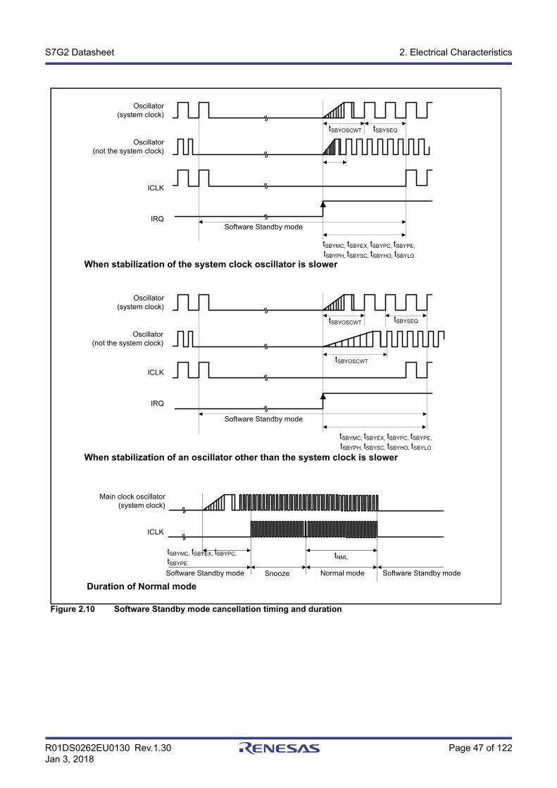
R01DS0262EU0130 Rev.1.30 Page 47 of 122Jan 3, 2018
S7G2 Datasheet 2. Electrical Characteristics
Figure 2.10 Software Standby mode cancellation timing and duration
Oscillator(system clock)
ICLK
IRQSoftware Standby mode
tSBYMC, tSBYEX, tSBYPC, tSBYPE,
tSBYPH, tSBYSC, tSBYHO, tSBYLO
Oscillator(not the system clock)
tSBYOSCWT tSBYSEQ
Oscillator(system clock)
ICLK
IRQ
Software Standby mode
tSBYMC, tSBYEX, tSBYPC, tSBYPE,
tSBYPH, tSBYSC, tSBYHO, tSBYLO
tSBYOSCWT
tSBYOSCWT
When stabilization of the system clock oscillator is slower
tSBYSEQ
Oscillator(not the system clock)
When stabilization of an oscillator other than the system clock is slower
Duration of Normal mode
Main clock oscillator(system clock)
tSBYMC, tSBYEX, tSBYPC,
tSBYPE
Normal modeSoftware Standby mode
tNML
ICLK
Software Standby modeSnooze
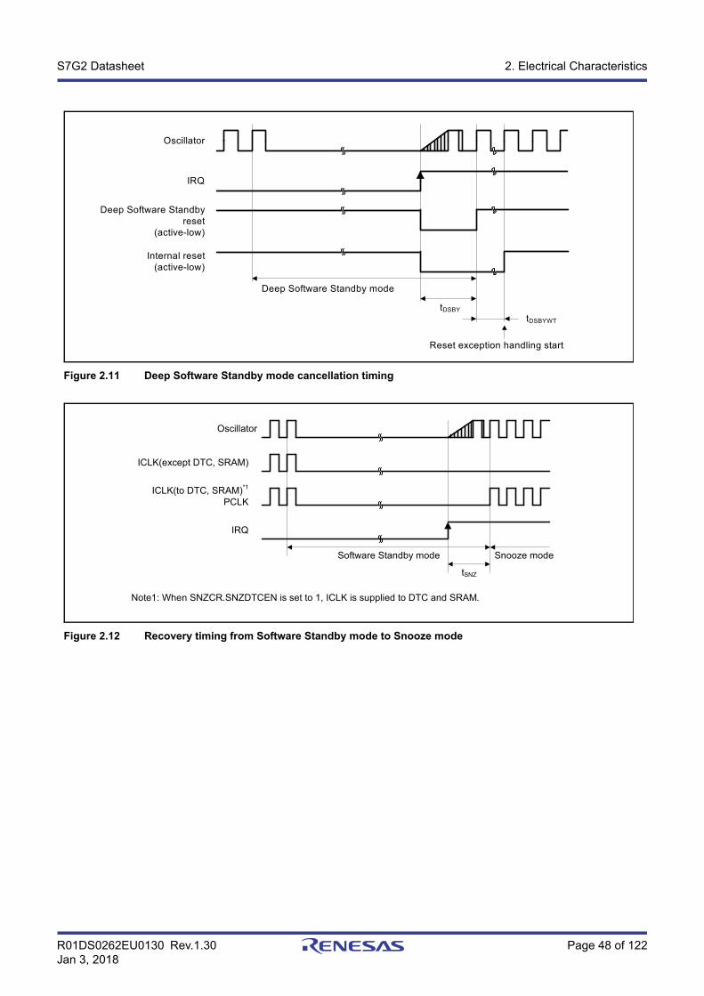
R01DS0262EU0130 Rev.1.30 Page 48 of 122Jan 3, 2018
S7G2 Datasheet 2. Electrical Characteristics
Figure 2.11 Deep Software Standby mode cancellation timing
Figure 2.12 Recovery timing from Software Standby mode to Snooze mode
Oscillator
IRQ
Internal reset(active-low)
Reset exception handling start
Deep Software Standby mode
Deep Software Standby reset
(active-low)
tDSBY
tDSBYWT
tSNZ
IRQ
ICLK(to DTC, SRAM)*1
PCLK
ICLK(except DTC, SRAM)
Note1: When SNZCR.SNZDTCEN is set to 1, ICLK is supplied to DTC and SRAM.
Oscillator
Software Standby mode Snooze mode
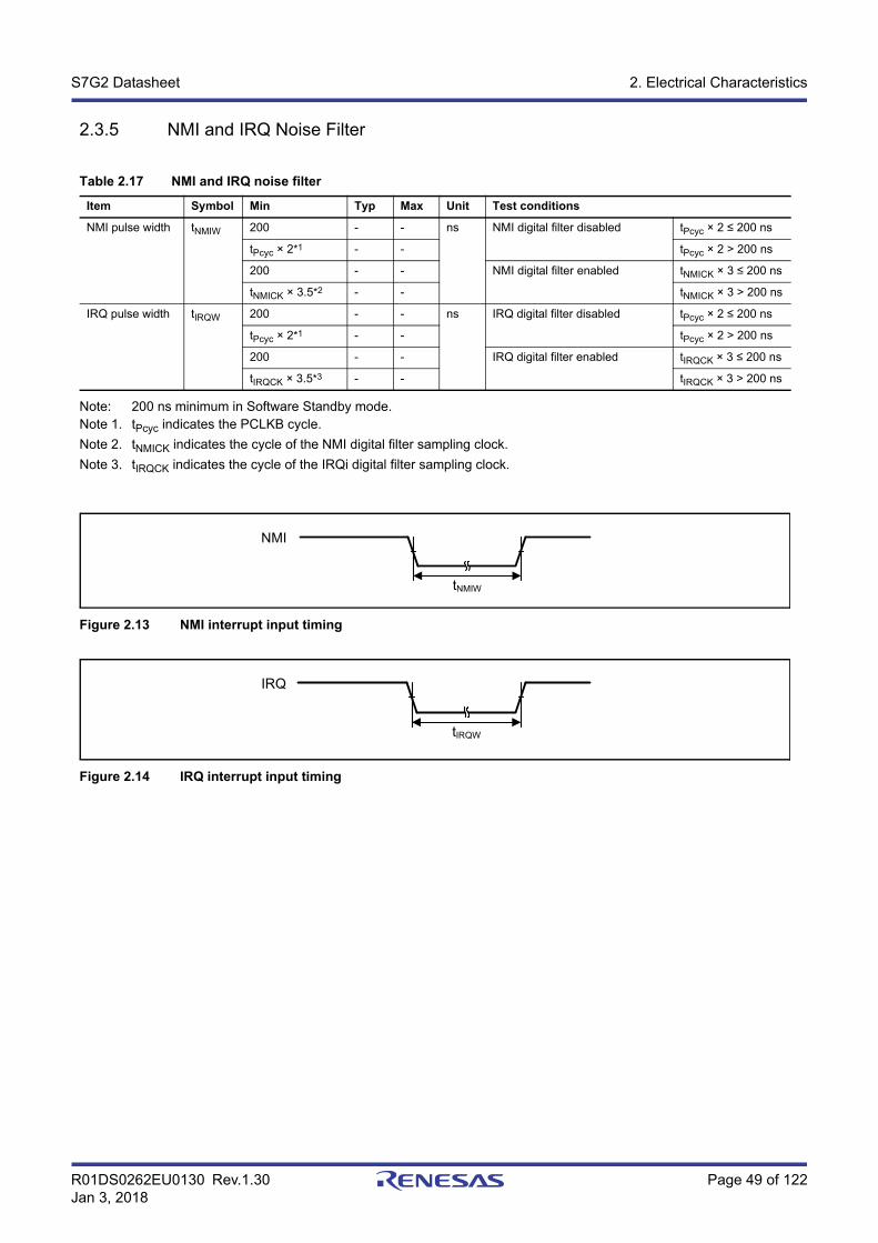
R01DS0262EU0130 Rev.1.30 Page 49 of 122Jan 3, 2018
S7G2 Datasheet 2. Electrical Characteristics
2.3.5 NMI and IRQ Noise Filter
Note: 200 ns minimum in Software Standby mode.Note 1. tPcyc indicates the PCLKB cycle.
Note 2. tNMICK indicates the cycle of the NMI digital filter sampling clock.
Note 3. tIRQCK indicates the cycle of the IRQi digital filter sampling clock.
Figure 2.13 NMI interrupt input timing
Figure 2.14 IRQ interrupt input timing
Table 2.17 NMI and IRQ noise filter
Item Symbol Min Typ Max Unit Test conditions
NMI pulse width tNMIW 200 - - ns NMI digital filter disabled tPcyc × 2 ≤ 200 ns
tPcyc × 2*1 - - tPcyc × 2 > 200 ns
200 - - NMI digital filter enabled tNMICK × 3 ≤ 200 ns
tNMICK × 3.5*2 - - tNMICK × 3 > 200 ns
IRQ pulse width tIRQW 200 - - ns IRQ digital filter disabled tPcyc × 2 ≤ 200 ns
tPcyc × 2*1 - - tPcyc × 2 > 200 ns
200 - - IRQ digital filter enabled tIRQCK × 3 ≤ 200 ns
tIRQCK × 3.5*3 - - tIRQCK × 3 > 200 ns
tNMIW
NMI
tIRQW
IRQ
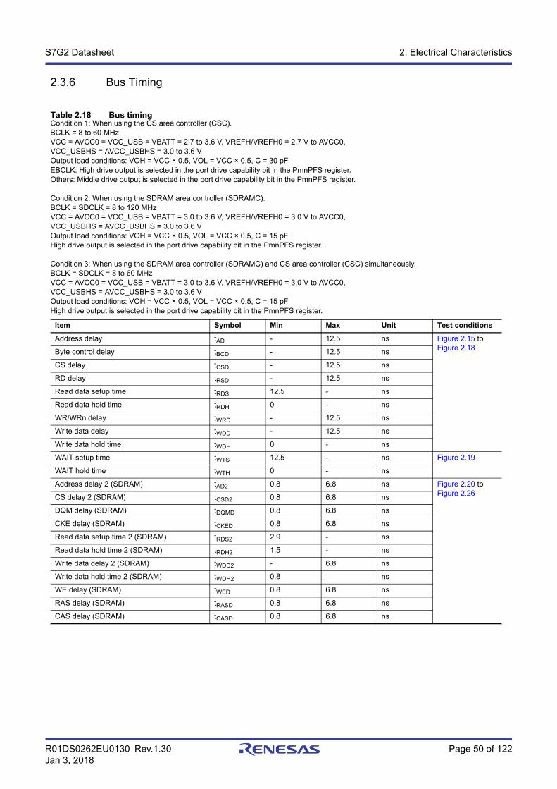
R01DS0262EU0130 Rev.1.30 Page 50 of 122Jan 3, 2018
S7G2 Datasheet 2. Electrical Characteristics
2.3.6 Bus Timing
Table 2.18 Bus timingCondition 1: When using the CS area controller (CSC).BCLK = 8 to 60 MHzVCC = AVCC0 = VCC_USB = VBATT = 2.7 to 3.6 V, VREFH/VREFH0 = 2.7 V to AVCC0,VCC_USBHS = AVCC_USBHS = 3.0 to 3.6 VOutput load conditions: VOH = VCC × 0.5, VOL = VCC × 0.5, C = 30 pFEBCLK: High drive output is selected in the port drive capability bit in the PmnPFS register.Others: Middle drive output is selected in the port drive capability bit in the PmnPFS register.
Condition 2: When using the SDRAM area controller (SDRAMC).BCLK = SDCLK = 8 to 120 MHzVCC = AVCC0 = VCC_USB = VBATT = 3.0 to 3.6 V, VREFH/VREFH0 = 3.0 V to AVCC0,VCC_USBHS = AVCC_USBHS = 3.0 to 3.6 VOutput load conditions: VOH = VCC × 0.5, VOL = VCC × 0.5, C = 15 pFHigh drive output is selected in the port drive capability bit in the PmnPFS register.
Condition 3: When using the SDRAM area controller (SDRAMC) and CS area controller (CSC) simultaneously.BCLK = SDCLK = 8 to 60 MHzVCC = AVCC0 = VCC_USB = VBATT = 3.0 to 3.6 V, VREFH/VREFH0 = 3.0 V to AVCC0,VCC_USBHS = AVCC_USBHS = 3.0 to 3.6 VOutput load conditions: VOH = VCC × 0.5, VOL = VCC × 0.5, C = 15 pFHigh drive output is selected in the port drive capability bit in the PmnPFS register.
Item Symbol Min Max Unit Test conditions
Address delay tAD - 12.5 ns Figure 2.15 to Figure 2.18Byte control delay tBCD - 12.5 ns
CS delay tCSD - 12.5 ns
RD delay tRSD - 12.5 ns
Read data setup time tRDS 12.5 - ns
Read data hold time tRDH 0 - ns
WR/WRn delay tWRD - 12.5 ns
Write data delay tWDD - 12.5 ns
Write data hold time tWDH 0 - ns
WAIT setup time tWTS 12.5 - ns Figure 2.19
WAIT hold time tWTH 0 - ns
Address delay 2 (SDRAM) tAD2 0.8 6.8 ns Figure 2.20 to Figure 2.26CS delay 2 (SDRAM) tCSD2 0.8 6.8 ns
DQM delay (SDRAM) tDQMD 0.8 6.8 ns
CKE delay (SDRAM) tCKED 0.8 6.8 ns
Read data setup time 2 (SDRAM) tRDS2 2.9 - ns
Read data hold time 2 (SDRAM) tRDH2 1.5 - ns
Write data delay 2 (SDRAM) tWDD2 - 6.8 ns
Write data hold time 2 (SDRAM) tWDH2 0.8 - ns
WE delay (SDRAM) tWED 0.8 6.8 ns
RAS delay (SDRAM) tRASD 0.8 6.8 ns
CAS delay (SDRAM) tCASD 0.8 6.8 ns
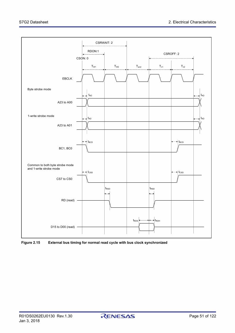
R01DS0262EU0130 Rev.1.30 Page 51 of 122Jan 3, 2018
S7G2 Datasheet 2. Electrical Characteristics
Figure 2.15 External bus timing for normal read cycle with bus clock synchronized
A23 to A01
CS7 to CS0
tAD
EBCLK
A23 to A00
D15 to D00 (read)
Byte strobe mode
1-write strobe mode
BC1, BC0
Common to both byte strobe mode and 1-write strobe mode
tBCD
tCSD tCSD
RD (read)
tRSD tRSD
tAD
tRDHtRDS
tAD
tAD
tBCD
TW1 TW2 Tend Tn1 Tn2
RDON:1
CSRWAIT: 2
CSROFF: 2
CSON: 0
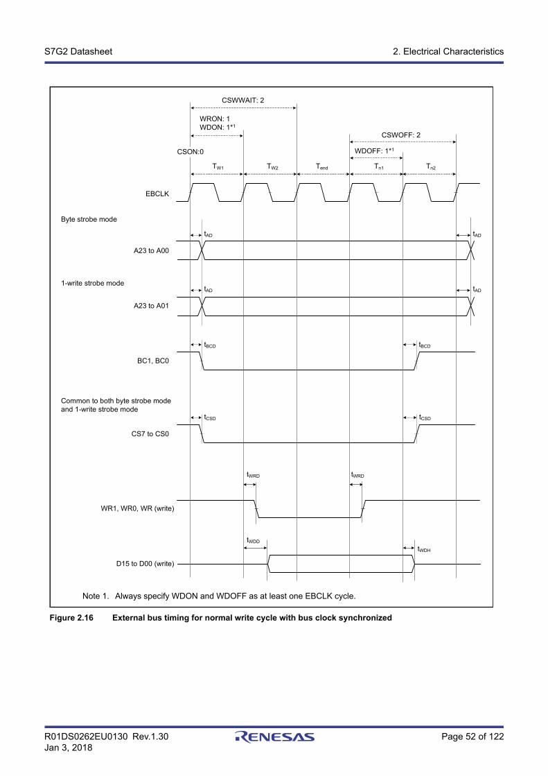
R01DS0262EU0130 Rev.1.30 Page 52 of 122Jan 3, 2018
S7G2 Datasheet 2. Electrical Characteristics
Figure 2.16 External bus timing for normal write cycle with bus clock synchronized
Note 1. Always specify WDON and WDOFF as at least one EBCLK cycle.
A23 to A01
CS7 to CS0
tAD
EBCLK
A23 to A00
Byte strobe mode
1-write strobe mode
BC1, BC0
Common to both byte strobe mode and 1-write strobe mode
tBCD
tCSD tCSD
tAD
tAD
tAD
tBCD
D15 to D00 (write)
WR1, WR0, WR (write)
tWRD tWRD
tWDH
tWDD
TW1 TW2 Tend Tn1 Tn2
WRON: 1WDON: 1*1
CSWWAIT: 2
WDOFF: 1*1CSON:0
CSWOFF: 2
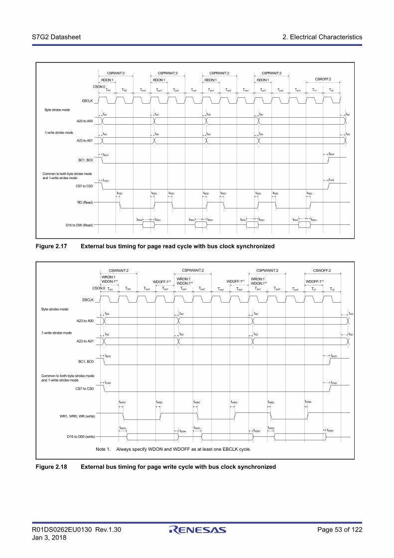
R01DS0262EU0130 Rev.1.30 Page 53 of 122Jan 3, 2018
S7G2 Datasheet 2. Electrical Characteristics
Figure 2.17 External bus timing for page read cycle with bus clock synchronized
Figure 2.18 External bus timing for page write cycle with bus clock synchronized
A23 to A01
CS7 to CS0
tAD
EBCLK
A23 to A00
D15 to D00 (Read)
Byte strobe mode
1-write strobe mode
BC1, BC0
Common to both byte strobe mode and 1-write strobe mode
tBCD
tCSDtCSD
RD (Read)
tRSD tRSD
tRDHtRDS
tAD
tBCD
TW1 TW2 Tend Tpw1 Tpw2
tAD tAD
tRSD tRSD
tRDHtRDS
tRSD tRSD
tRDHtRDS
Tend Tpw1 Tpw2 Tend Tn1 Tn2
tAD tAD tAD tAD
RDON:1
CSRWAIT:2
CSROFF:2
tRSD tRSD
tRDHtRDS
tAD
tAD
CSPRWAIT:2
Tpw1 Tpw2 Tend
RDON:1
CSPRWAIT:2
RDON:1
CSPRWAIT:2
RDON:1
CSON:0
Note 1. Always specify WDON and WDOFF as at least one EBCLK cycle.
A23 to A01
CS7 to CS0
tAD
EBCLK
A23 to A00
Byte strobe mode
1-write strobe mode
BC1, BC0
Common to both byte strobe mode and 1-write strobe mode
tBCD
tCSD tCSD
tAD
tBCD
TW1
D15 to D00 (write)
WR1, WR0, WR (write)
tWRD tWRD
tWDH
tWDD
TW2 Tend Tpw1 Tpw2
tAD tAD
tWRD tWRD
tWDH
tWDD
tWRD tWRD
tWDHtWDD
Tdw1 Tend Tpw1 Tpw2 Tend Tn1 Tn2Tdw1
tAD tAD tAD tAD
WRON:1WDON:1*1
CSWWAIT:2 CSPWWAIT:2
WDOFF:1*1
CSPWWAIT:2
WDOFF:1*1 WDOFF:1*1
CSON:0
WRON:1WDON:1*1
WRON:1WDON:1*1
CSWOFF:2
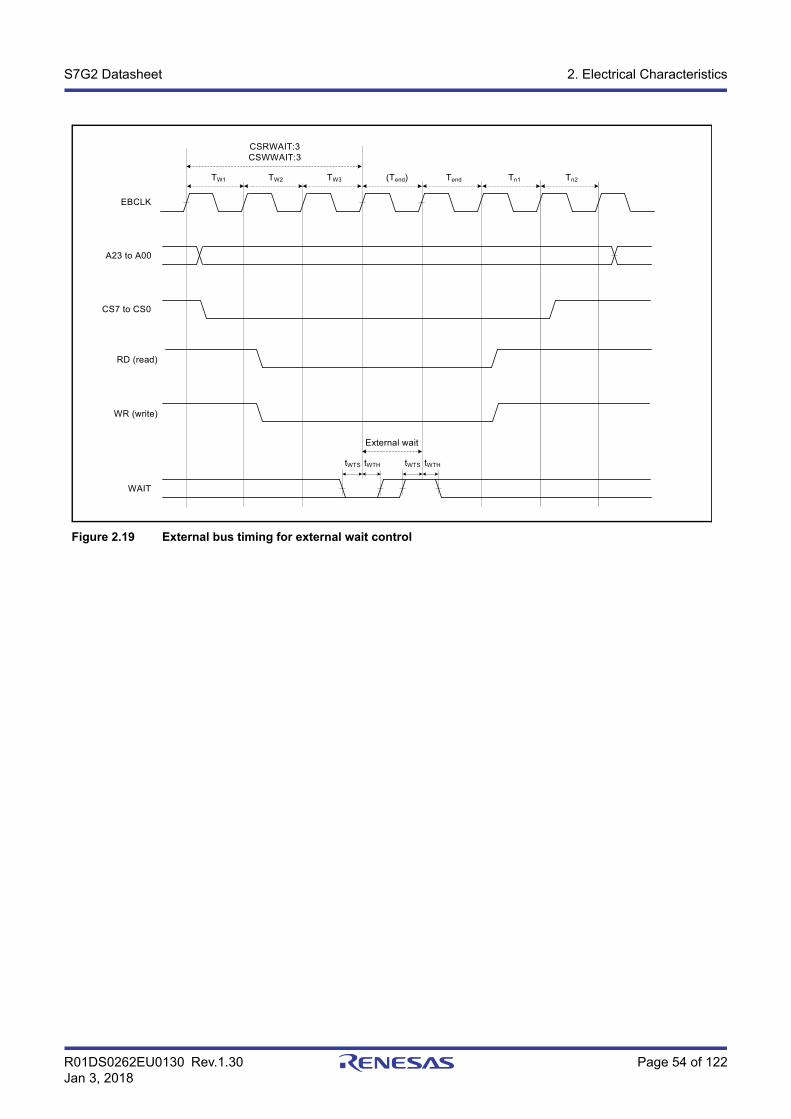
R01DS0262EU0130 Rev.1.30 Page 54 of 122Jan 3, 2018
S7G2 Datasheet 2. Electrical Characteristics
Figure 2.19 External bus timing for external wait control
tWTS tWTH tWTS tWTH
CSRWAIT:3CSWWAIT:3
EBCLK
A23 to A00
CS7 to CS0
RD (read)
WR (write)
WAIT
TW1 TW2 (Tend) TendTW3 Tn1 Tn2
External wait
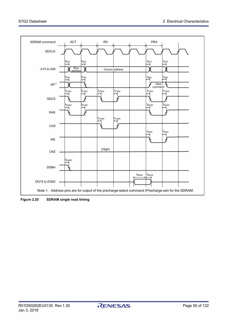
R01DS0262EU0130 Rev.1.30 Page 55 of 122Jan 3, 2018
S7G2 Datasheet 2. Electrical Characteristics
Figure 2.20 SDRAM single read timing
Note 1. Address pins are for output of the precharge-select command (Precharge-sel) for the SDRAM.
tAD2
SDCLK
A15 to A00
SDCS
AP*1
DQMn
DQ15 to DQ00
RAS
CAS
WE
CKE
tDQMD
(High)
Rowaddress Column address
SDRAM command ACT RD PRA
tAD2
tCSD2
tRASD
tAD2
tAD2
tCSD2
tRASD
tAD2
tAD2
tCSD2
tRASD
tAD2
tAD2
tCSD2
tRASD
tWED tWED
tCSD2 tCSD2
tCASD tCASD
tRDS2 tRDH2
PRAcommand
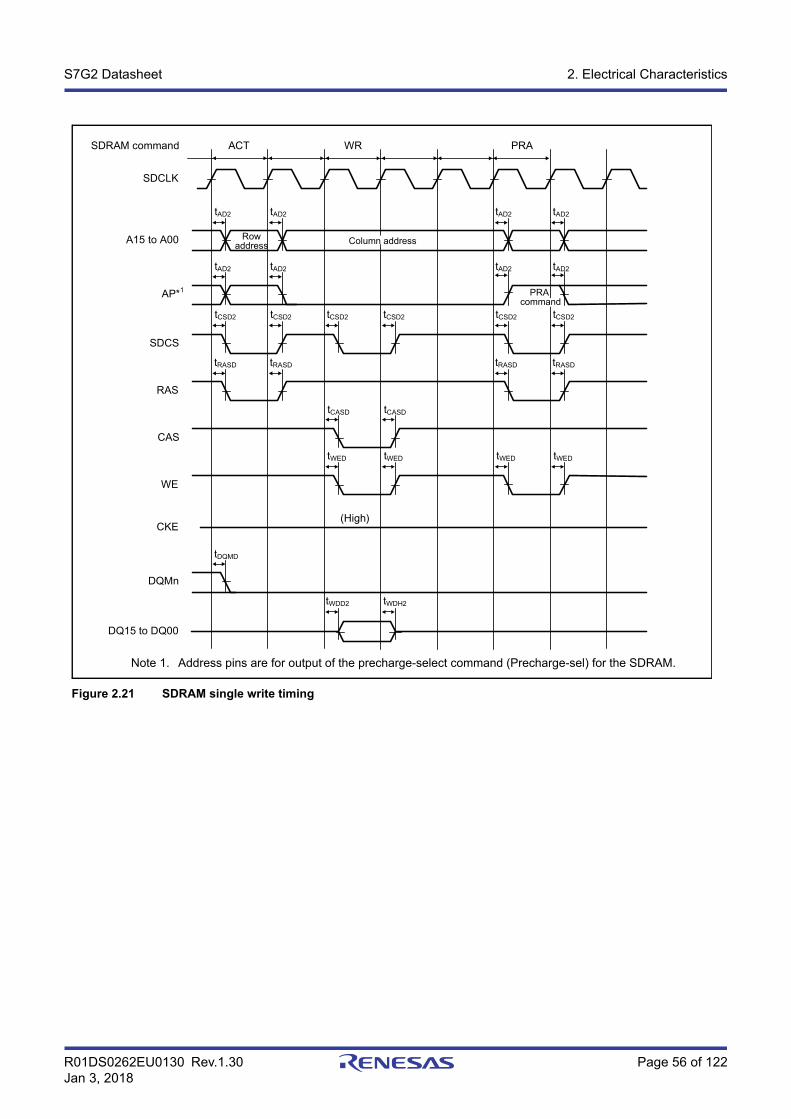
R01DS0262EU0130 Rev.1.30 Page 56 of 122Jan 3, 2018
S7G2 Datasheet 2. Electrical Characteristics
Figure 2.21 SDRAM single write timing
Note 1. Address pins are for output of the precharge-select command (Precharge-sel) for the SDRAM.
tAD2
SDCLK
A15 to A00
SDCS
AP*1
DQMn
DQ15 to DQ00
RAS
CAS
WE
CKE
tDQMD
(High)
Rowaddress Column address
SDRAM command ACT WR PRA
tAD2
tCSD2
tRASD
tWED
tCASD
tWDD2
tAD2
tAD2
tCSD2
tRASD
tAD2
tAD2
tCSD2
tRASD
tAD2
tAD2
tCSD2
tRASD
tCSD2 tCSD2
tCASD
tWED tWED tWED
tWDH2
PRAcommand
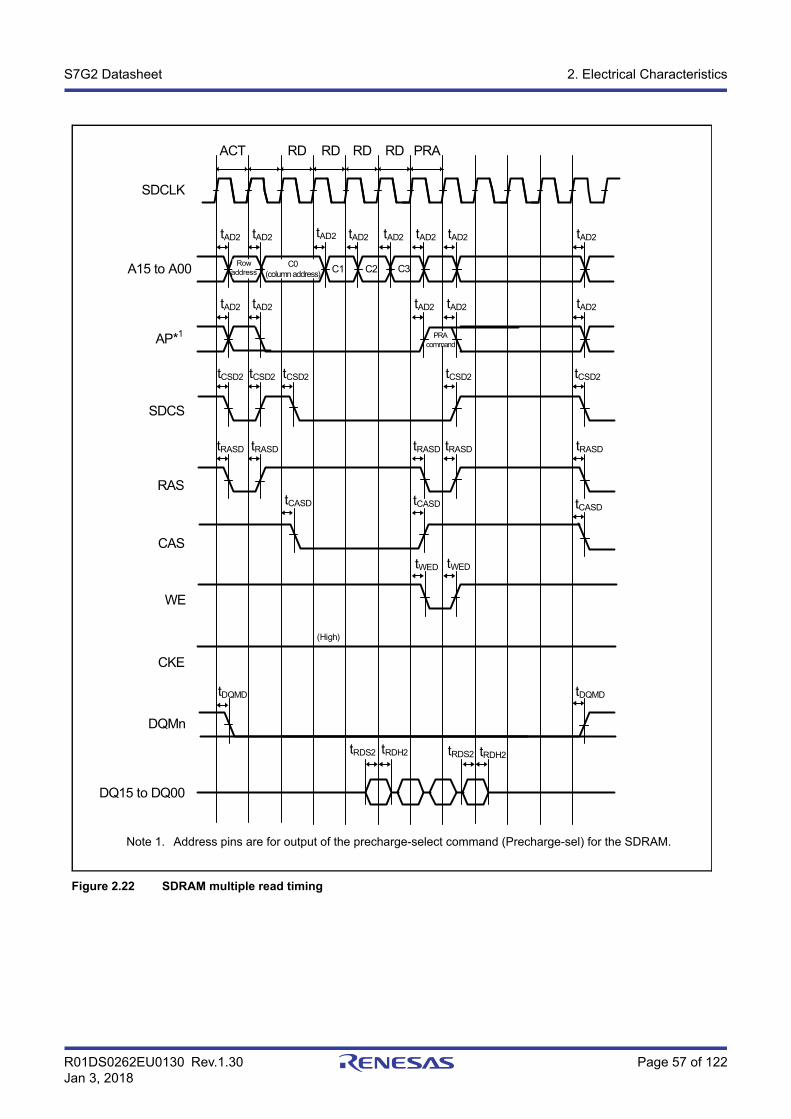
R01DS0262EU0130 Rev.1.30 Page 57 of 122Jan 3, 2018
S7G2 Datasheet 2. Electrical Characteristics
Figure 2.22 SDRAM multiple read timing
Note 1. Address pins are for output of the precharge-select command (Precharge-sel) for the SDRAM.
SDCLK
ACT RD RD RD RD PRA
A15 to A00
tAD2 tAD2 tAD2 tAD2 tAD2 tAD2 tAD2 tAD2
AP*1
SDCS
RAS
CAS
WE
CKE
DQMn
DQ15 to DQ00
C1 C2 C3Row
addressC0
(column address)
tAD2 tAD2 tAD2 tAD2 tAD2
tCSD2 tCSD2 tCSD2 tCSD2 tCSD2
tRASD tRASD tRASD tRASD tRASD
tCASD tCASD tCASD
tWED tWED
(High)
tDQMD tDQMD
tRDS2 tRDH2 tRDS2 tRDH2
PRAcommand
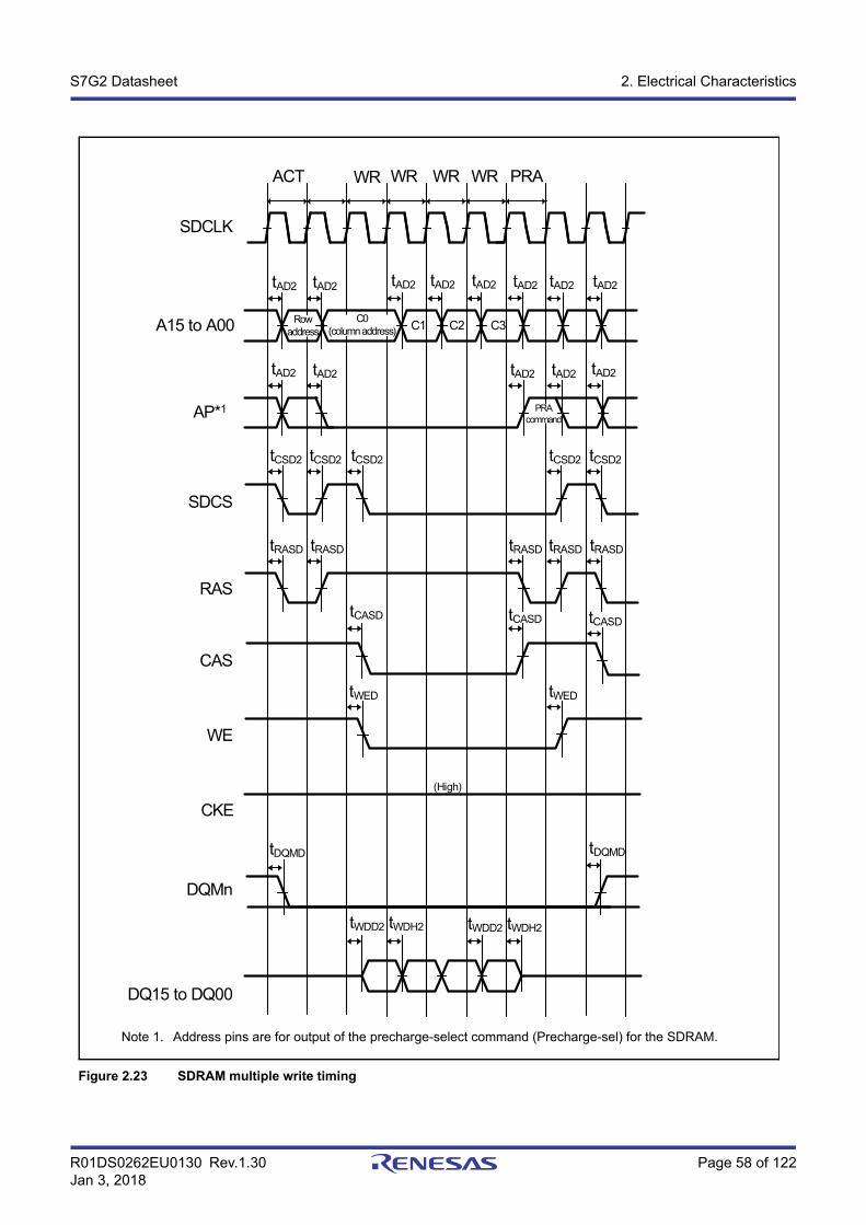
R01DS0262EU0130 Rev.1.30 Page 58 of 122Jan 3, 2018
S7G2 Datasheet 2. Electrical Characteristics
Figure 2.23 SDRAM multiple write timing
Note 1. Address pins are for output of the precharge-select command (Precharge-sel) for the SDRAM.
ACT WR PRAWR WR WR
SDCLK
A15 to A00
AP*1
SDCS
RAS
CAS
WE
CKE
DQMn
DQ15 to DQ00
tAD2 tAD2 tAD2 tAD2 tAD2 tAD2 tAD2 tAD2
tAD2 tAD2 tAD2 tAD2 tAD2
tCSD2 tCSD2 tCSD2 tCSD2 tCSD2
tRASD tRASD tRASD tRASD tRASD
tCASD tCASD tCASD
tWED tWED
(High)
tDQMD tDQMD
tWDD2 tWDH2 tWDD2 tWDH2
C1 C2 C3Rowaddress
C0(column address)
PRAcommand
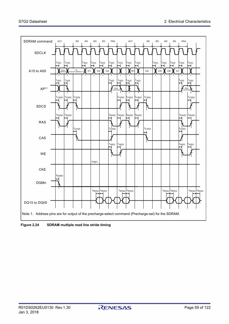
R01DS0262EU0130 Rev.1.30 Page 59 of 122Jan 3, 2018
S7G2 Datasheet 2. Electrical Characteristics
Figure 2.24 SDRAM multiple read line stride timing
Note 1. Address pins are for output of the precharge-select command (Precharge-sel) for the SDRAM.
R1A15 to A00
SDCLK
SDCS
AP*1
DQMn
DQ15 to DQ00
RAS
CAS
WE
CKE
SDRAM command ACT RD RD RD RD PRA ACT RD RD RD RD PRA
tCASD
tRASD
t CSD2
t AD2 t AD2 t AD2 t AD2 t AD2 t AD2 t AD2 t AD2 t AD2 t AD2 t AD2 t AD2 t AD2 t AD2
t AD2 t AD2 t AD2 t AD2 t AD2 t AD2 t AD2 t AD2
t CSD2 t CSD2 t CSD2 tCSD2 tCSD2 tCSD2 tCSD2
tRASD tRASD tRASD tRASD tRASD
tCASD tCASD
tRASD tRASD
tCASD
tDQMD
t RDS2 tRDH2 t RDS2 tRDH2 t RDS2 tRDH2 t RDS2 tRDH2
(High)
Rowaddress
C0(column address 0) C1 C2 C3 C4 C5 C6 C7
PRAcommand
PRAcommand
t WED t WED t WED t WED
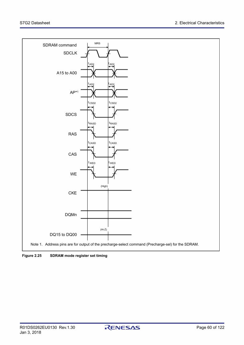
R01DS0262EU0130 Rev.1.30 Page 60 of 122Jan 3, 2018
S7G2 Datasheet 2. Electrical Characteristics
Figure 2.25 SDRAM mode register set timing
Note 1. Address pins are for output of the precharge-select command (Precharge-sel) for the SDRAM.
A15 to A00
SDCLK
SDCS
AP*1
DQMn
DQ15 to DQ00
RAS
CAS
WE
CKE
SDRAM command
(Hi-Z)
(High)
tCASD
tRASD
t CSD2
t AD2
MRS
t AD2
t AD2
t AD2
tCASD
tRASD
tCSD2
t WED t WED
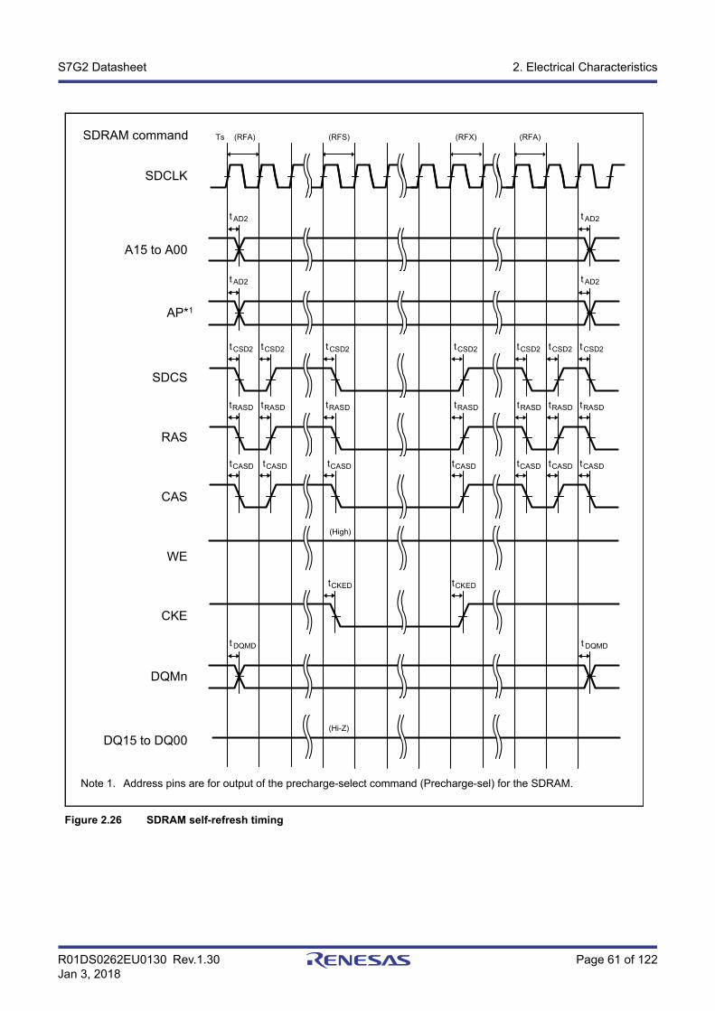
R01DS0262EU0130 Rev.1.30 Page 61 of 122Jan 3, 2018
S7G2 Datasheet 2. Electrical Characteristics
Figure 2.26 SDRAM self-refresh timing
Note 1. Address pins are for output of the precharge-select command (Precharge-sel) for the SDRAM.
A15 to A00
(RFS)
SDCLK
SDCS
AP*1
DQMn
DQ15 to DQ00
RAS
CAS
WE
CKE
(Hi-Z)
tCKED
(High)
tCASDtCASDtCASD
tRASD tRASD tRASD
t CSD2tCSD2tCSD2
t AD2
t AD2
(RFA)Ts (RFX) (RFA)
t AD2
t AD2
tCSD2 t CSD2tCSD2tCSD2
tRASD tRASD tRASD tRASD
tCASD tCASD tCASD tCASD
tCKED
SDRAM command
t DQMD t DQMD
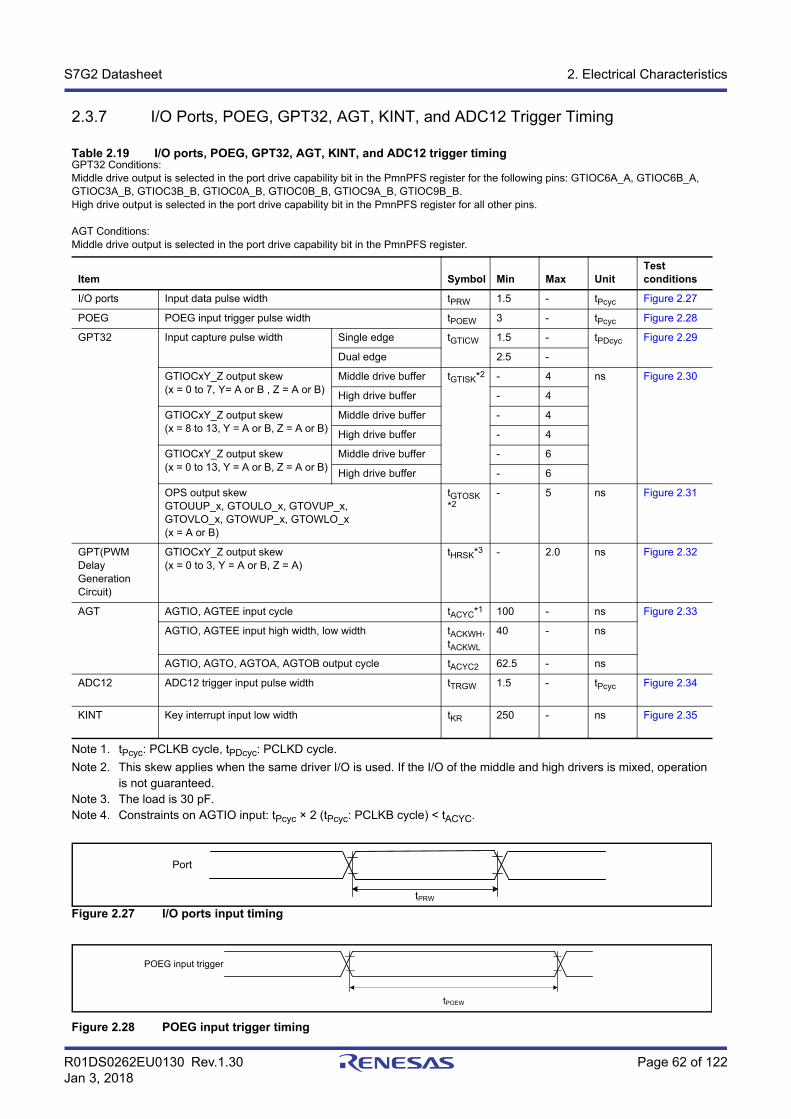
R01DS0262EU0130 Rev.1.30 Page 62 of 122Jan 3, 2018
S7G2 Datasheet 2. Electrical Characteristics
2.3.7 I/O Ports, POEG, GPT32, AGT, KINT, and ADC12 Trigger Timing
Note 1. tPcyc: PCLKB cycle, tPDcyc: PCLKD cycle.
Note 2. This skew applies when the same driver I/O is used. If the I/O of the middle and high drivers is mixed, operation is not guaranteed.
Note 3. The load is 30 pF.Note 4. Constraints on AGTIO input: tPcyc × 2 (tPcyc: PCLKB cycle) < tACYC.
Figure 2.27 I/O ports input timing
Figure 2.28 POEG input trigger timing
Table 2.19 I/O ports, POEG, GPT32, AGT, KINT, and ADC12 trigger timingGPT32 Conditions:Middle drive output is selected in the port drive capability bit in the PmnPFS register for the following pins: GTIOC6A_A, GTIOC6B_A, GTIOC3A_B, GTIOC3B_B, GTIOC0A_B, GTIOC0B_B, GTIOC9A_B, GTIOC9B_B.High drive output is selected in the port drive capability bit in the PmnPFS register for all other pins.
AGT Conditions:Middle drive output is selected in the port drive capability bit in the PmnPFS register.
Item Symbol Min Max UnitTest conditions
I/O ports Input data pulse width tPRW 1.5 - tPcyc Figure 2.27
POEG POEG input trigger pulse width tPOEW 3 - tPcyc Figure 2.28
GPT32 Input capture pulse width Single edge tGTICW 1.5 - tPDcyc Figure 2.29
Dual edge 2.5 -
GTIOCxY_Z output skew(x = 0 to 7, Y= A or B , Z = A or B)
Middle drive buffer tGTISK*2 - 4 ns Figure 2.30
High drive buffer - 4
GTIOCxY_Z output skew(x = 8 to 13, Y = A or B, Z = A or B)
Middle drive buffer - 4
High drive buffer - 4
GTIOCxY_Z output skew(x = 0 to 13, Y = A or B, Z = A or B)
Middle drive buffer - 6
High drive buffer - 6
OPS output skewGTOUUP_x, GTOULO_x, GTOVUP_x,GTOVLO_x, GTOWUP_x, GTOWLO_x(x = A or B)
tGTOSK*2
- 5 ns Figure 2.31
GPT(PWM Delay Generation Circuit)
GTIOCxY_Z output skew (x = 0 to 3, Y = A or B, Z = A)
tHRSK*3 - 2.0 ns Figure 2.32
AGT AGTIO, AGTEE input cycle tACYC*1 100 - ns Figure 2.33
AGTIO, AGTEE input high width, low width tACKWH, tACKWL
40 - ns
AGTIO, AGTO, AGTOA, AGTOB output cycle tACYC2 62.5 - ns
ADC12 ADC12 trigger input pulse width tTRGW 1.5 - tPcyc Figure 2.34
KINT Key interrupt input low width tKR 250 - ns Figure 2.35
Port
tPRW
POEG input trigger
tPOEW
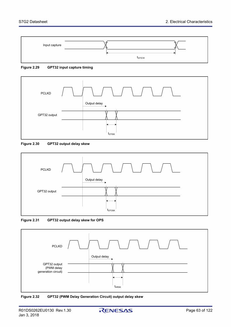
R01DS0262EU0130 Rev.1.30 Page 63 of 122Jan 3, 2018
S7G2 Datasheet 2. Electrical Characteristics
Figure 2.29 GPT32 input capture timing
Figure 2.30 GPT32 output delay skew
Figure 2.31 GPT32 output delay skew for OPS
Figure 2.32 GPT32 (PWM Delay Generation Circuit) output delay skew
Input capture
tGTICW
GPT32 output
PCLKD
tGTISK
Output delay
GPT32 output
PCLKD
tGTOSK
Output delay
GPT32 output(PWM delay
generation circuit)
PCLKD
tHRSK
Output delay
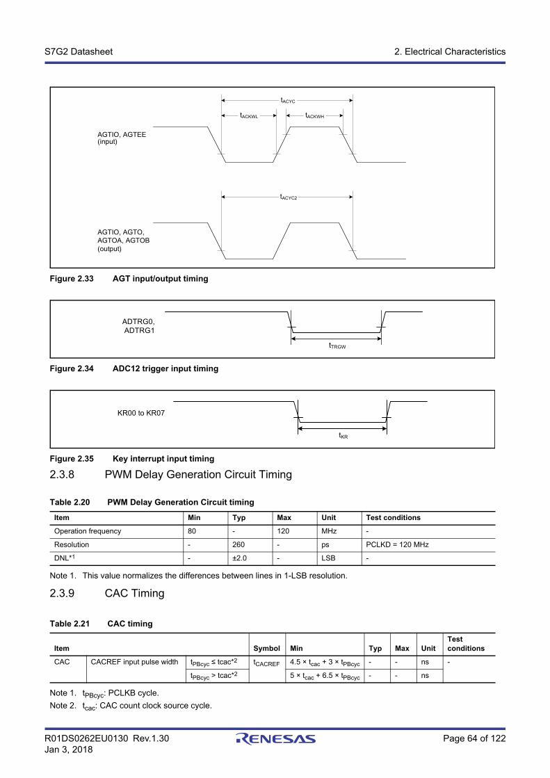
R01DS0262EU0130 Rev.1.30 Page 64 of 122Jan 3, 2018
S7G2 Datasheet 2. Electrical Characteristics
Figure 2.33 AGT input/output timing
Figure 2.34 ADC12 trigger input timing
Figure 2.35 Key interrupt input timing
2.3.8 PWM Delay Generation Circuit Timing
Note 1. This value normalizes the differences between lines in 1-LSB resolution.
2.3.9 CAC Timing
Note 1. tPBcyc: PCLKB cycle.
Note 2. tcac: CAC count clock source cycle.
Table 2.20 PWM Delay Generation Circuit timing
Item Min Typ Max Unit Test conditions
Operation frequency 80 - 120 MHz -
Resolution - 260 - ps PCLKD = 120 MHz
DNL*1 - ±2.0 - LSB -
Table 2.21 CAC timing
Item Symbol Min Typ Max UnitTest conditions
CAC CACREF input pulse width tPBcyc ≤ tcac*2 tCACREF 4.5 × tcac + 3 × tPBcyc - - ns -
tPBcyc > tcac*2 5 × tcac + 6.5 × tPBcyc - - ns
tACYC2
AGTIO, AGTEE(input)
tACYC
tACKWL tACKWH
AGTIO, AGTO,AGTOA, AGTOB(output)
ADTRG0, ADTRG1
tTRGW
KR00 to KR07
tKR
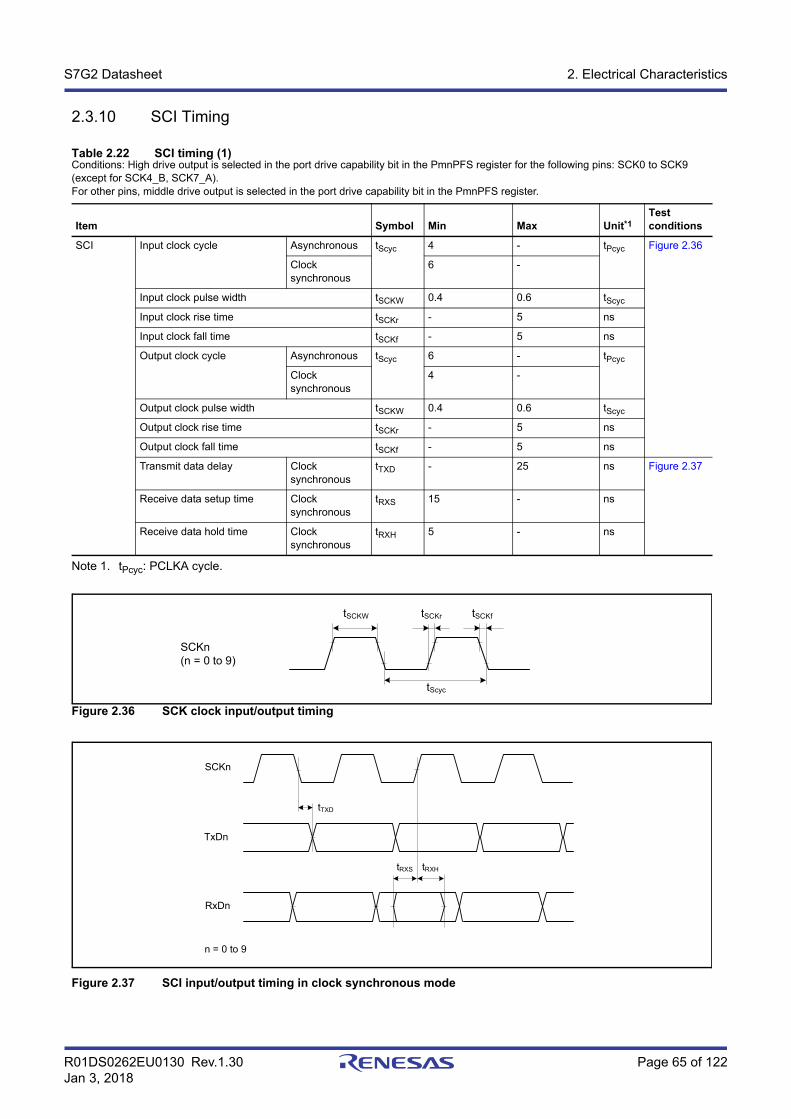
R01DS0262EU0130 Rev.1.30 Page 65 of 122Jan 3, 2018
S7G2 Datasheet 2. Electrical Characteristics
2.3.10 SCI Timing
Note 1. tPcyc: PCLKA cycle.
Figure 2.36 SCK clock input/output timing
Figure 2.37 SCI input/output timing in clock synchronous mode
Table 2.22 SCI timing (1)Conditions: High drive output is selected in the port drive capability bit in the PmnPFS register for the following pins: SCK0 to SCK9 (except for SCK4_B, SCK7_A).For other pins, middle drive output is selected in the port drive capability bit in the PmnPFS register.
Item Symbol Min Max Unit*1Test conditions
SCI Input clock cycle Asynchronous tScyc 4 - tPcyc Figure 2.36
Clock synchronous
6 -
Input clock pulse width tSCKW 0.4 0.6 tScyc
Input clock rise time tSCKr - 5 ns
Input clock fall time tSCKf - 5 ns
Output clock cycle Asynchronous tScyc 6 - tPcyc
Clock synchronous
4 -
Output clock pulse width tSCKW 0.4 0.6 tScyc
Output clock rise time tSCKr - 5 ns
Output clock fall time tSCKf - 5 ns
Transmit data delay Clock synchronous
tTXD - 25 ns Figure 2.37
Receive data setup time Clock synchronous
tRXS 15 - ns
Receive data hold time Clock synchronous
tRXH 5 - ns
tSCKW tSCKr tSCKf
tScyc
SCKn(n = 0 to 9)
tTXD
tRXS tRXH
TxDn
RxDn
SCKn
n = 0 to 9
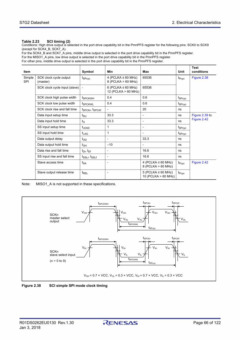
R01DS0262EU0130 Rev.1.30 Page 66 of 122Jan 3, 2018
S7G2 Datasheet 2. Electrical Characteristics
Note: MISO1_A is not supported in these specifications.
Figure 2.38 SCI simple SPI mode clock timing
Table 2.23 SCI timing (2)Conditions: High drive output is selected in the port drive capability bit in the PmnPFS register for the following pins: SCK0 to SCK9 (except for SCK4_B, SCK7_A).For the SCK4_B and SCK7_A pins, middle drive output is selected in the port drive capability bit in the PmnPFS register.For the MISO1_A pins, low drive output is selected in the port drive capability bit in the PmnPFS register.For other pins, middle drive output is selected in the port drive capability bit in the PmnPFS register.
Item Symbol Min Max UnitTest conditions
Simple SPI
SCK clock cycle output (master)
tSPcyc 4 (PCLKA ≤ 60 MHz)8 (PCLKA > 60 MHz)
65536 tPcyc Figure 2.38
SCK clock cycle input (slave) - 6 (PCLKA ≤ 60 MHz)12 (PCLKA > 60 MHz)
65536
SCK clock high pulse width tSPCKWH 0.4 0.6 tSPcyc
SCK clock low pulse width tSPCKWL 0.4 0.6 tSPcyc
SCK clock rise and fall time tSPCKr, tSPCKf - 20 ns
Data input setup time tSU 33.3 - ns Figure 2.39 to Figure 2.42
Data input hold time tH 33.3 - ns
SS input setup time tLEAD 1 - tSPcyc
SS input hold time tLAG 1 - tSPcyc
Data output delay tOD - 33.3 ns
Data output hold time tOH –10 - ns
Data rise and fall time tDr, tDf - 16.6 ns
SS input rise and fall time tSSLr, tSSLf - 16.6 ns
Slave access time tSA - 4 (PCLKA ≤ 60 MHz)8 (PCLKA > 60 MHz)
tPcyc Figure 2.42
Slave output release time tREL - 5 (PCLKA ≤ 60 MHz)10 (PCLKA > 60 MHz)
tPcyc
tSPCKWH
VOH VOH
VOL VOL
VOH VOH
tSPCKWL
tSPCKr tSPCKf
VOL
tSPcyc
tSPCKWH
VIH VIH
VIL VIL
VIH VIH
tSPCKWL
tSPCKr tSPCKf
VIL
tSPcyc
VOH = 0.7 × VCC, VOL = 0.3 × VCC, VIH = 0.7 × VCC, VIL = 0.3 × VCC
(n = 0 to 9)
SCKnmaster select output
SCKnslave select input
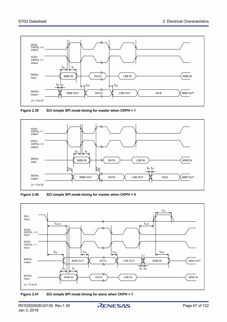
R01DS0262EU0130 Rev.1.30 Page 67 of 122Jan 3, 2018
S7G2 Datasheet 2. Electrical Characteristics
Figure 2.39 SCI simple SPI mode timing for master when CKPH = 1
Figure 2.40 SCI simple SPI mode timing for master when CKPH = 0
Figure 2.41 SCI simple SPI mode timing for slave when CKPH = 1
tDr, tDf
tSU tH
tOH tOD
MSB IN DATA LSB IN MSB IN
MSB OUT DATA LSB OUT IDLE MSB OUT
SCKnCKPOL = 0output
SCKnCKPOL = 1output
MISOninput
MOSInoutput
(n = 0 to 9)
tSU tH
tOH tOD
MSB IN DATA LSB IN MSB IN
MSB OUT DATA LSB OUT IDLE MSB OUT
SCKnCKPOL = 1output
SCKnCKPOL = 0output
MISOninput
MOSInoutput
(n = 0 to 9)
tDr, tDf
tDr, tDftSU tH
tLEAD
tTD
tLAG
tSA
MSB IN DATA LSB IN MSB IN
MSB OUT DATA LSB OUT MSB IN MSB OUT
tOH tOD tREL
SSninput
SCKnCKPOL = 0input
SCKnCKPOL = 1input
MISOnoutput
MOSIninput
(n = 0 to 9)
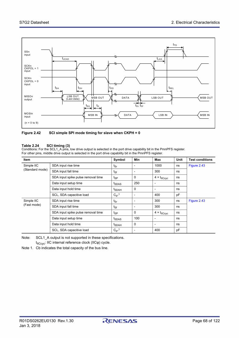
R01DS0262EU0130 Rev.1.30 Page 68 of 122Jan 3, 2018
S7G2 Datasheet 2. Electrical Characteristics
Figure 2.42 SCI simple SPI mode timing for slave when CKPH = 0
Note: SCL1_A output is not supported in these specifications.tIICcyc: IIC internal reference clock (IICφ) cycle.
Note 1. Cb indicates the total capacity of the bus line.
Table 2.24 SCI timing (3)Conditions: For the SCL1_A pins, low drive output is selected in the port drive capability bit in the PmnPFS register.For other pins, middle drive output is selected in the port drive capability bit in the PmnPFS register.
Item Symbol Min Max Unit Test conditions
Simple IIC(Standard mode)
SDA input rise time tSr - 1000 ns Figure 2.43
SDA input fall time tSf - 300 ns
SDA input spike pulse removal time tSP 0 4 × tIICcyc ns
Data input setup time tSDAS 250 - ns
Data input hold time tSDAH 0 - ns
SCL, SDA capacitive load Cb*1 - 400 pF
Simple IIC(Fast mode)
SDA input rise time tSr - 300 ns Figure 2.43
SDA input fall time tSf - 300 ns
SDA input spike pulse removal time tSP 0 4 × tIICcyc ns
Data input setup time tSDAS 100 - ns
Data input hold time tSDAH 0 - ns
SCL, SDA capacitive load Cb*1 - 400 pF
tDr, tDf
tSA tOH
tLEAD
tTD
tLAG
tH
LSB OUT(Last data) DATA MSB OUT
MSB IN DATA LSB IN MSB IN
LSB OUT
tSU
tOD tREL
MSB OUT
SSninput
SCKnCKPOL = 1input
SCKnCKPOL = 0input
MISOnoutput
MOSIninput
(n = 0 to 9)
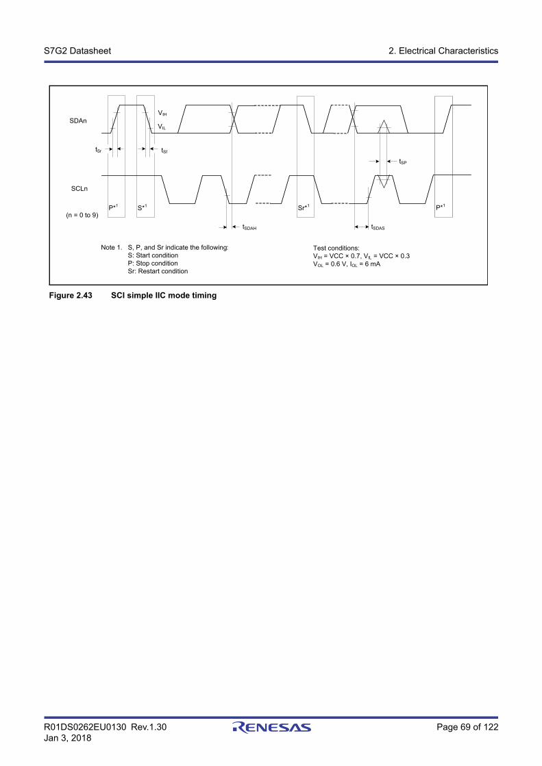
R01DS0262EU0130 Rev.1.30 Page 69 of 122Jan 3, 2018
S7G2 Datasheet 2. Electrical Characteristics
Figure 2.43 SCI simple IIC mode timing
SDAn
SCLn
VIH
VIL
P*1 S*1
tSftSr
tSDAH tSDAS
tSP
P*1
Test conditions:VIH = VCC × 0.7, VIL = VCC × 0.3VOL = 0.6 V, IOL = 6 mA
Sr*1
Note 1. S, P, and Sr indicate the following:S: Start conditionP: Stop conditionSr: Restart condition
(n = 0 to 9)
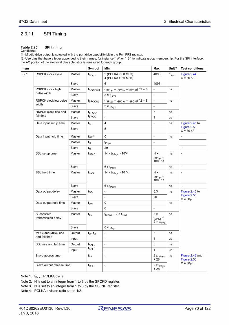
R01DS0262EU0130 Rev.1.30 Page 70 of 122Jan 3, 2018
S7G2 Datasheet 2. Electrical Characteristics
2.3.11 SPI Timing
Note 1. tPcyc: PCLKA cycle.
Note 2. N is set to an integer from 1 to 8 by the SPCKD register.Note 3. N is set to an integer from 1 to 8 by the SSLND register.Note 4. PCLKA division ratio set to 1/2.
Table 2.25 SPI timingConditions:(1) Middle drive output is selected with the port drive capability bit in the PmnPFS register.(2) Use pins that have a letter appended to their names, for instance “_A” or “_B”, to indicate group membership. For the SPI interface, the AC portion of the electrical characteristics is measured for each group.
Item Symbol Min Max Unit*1 Test conditions
SPI RSPCK clock cycle Master tSPcyc 2 (PCLKA 60 MHz)4 (PCLKA > 60 MHz)
4096 tPcyc Figure 2.44C = 30 pF
Slave 6 4096
RSPCK clock high pulse width
Master tSPCKWH (tSPcyc – tSPCKr – tSPCKf) / 2 – 3 - ns
Slave 3 × tPcyc -
RSPCK clock low pulse width
Master tSPCKWL (tSPcyc – tSPCKr – tSPCKf) / 2 – 3 - ns
Slave 3 × tPcyc -
RSPCK clock rise and fall time
Master tSPCKr, tSPCKf
- 5 ns
Slave - 1 µs
Data input setup time Master tSU 4 - ns Figure 2.45 toFigure 2.50C = 30 pF
Slave 5 -
Data input hold time Master tHF*4 0 - ns -
Master tH tPcyc -
Slave tH 20 - -
SSL setup time Master tLEAD N × tSPcyc - 10*2 N × tSPcyc + 100 *2
ns -
Slave 6 x tPcyc - ns -
SSL hold time Master tLAG N × tSPcyc - 10 *3 N × tSPcyc + 100 *3
ns -
Slave 6 x tPcyc - ns -
Data output delay Master tOD - 6.3 ns Figure 2.45 to Figure 2.50C = 30PF
Slave - 20
Data output hold time Master tOH 0 - ns
Slave 0 -
Successive transmission delay
Master tTD tSPcyc + 2 × tPcyc 8 × tSPcyc + 2 × tPcyc
ns
Slave 6 × tPcyc
MOSI and MISO rise and fall time
Output tDr, tDf - 5 ns
Input - 1 μs
SSL rise and fall time Output tSSLr, tSSLf
- 5 ns
Input - 1 μs
Slave access time tSA - 2 x tPcyc + 28
ns Figure 2.49 and Figure 2.50C = 30PF
Slave output release time tREL - 2 x tPcyc + 28
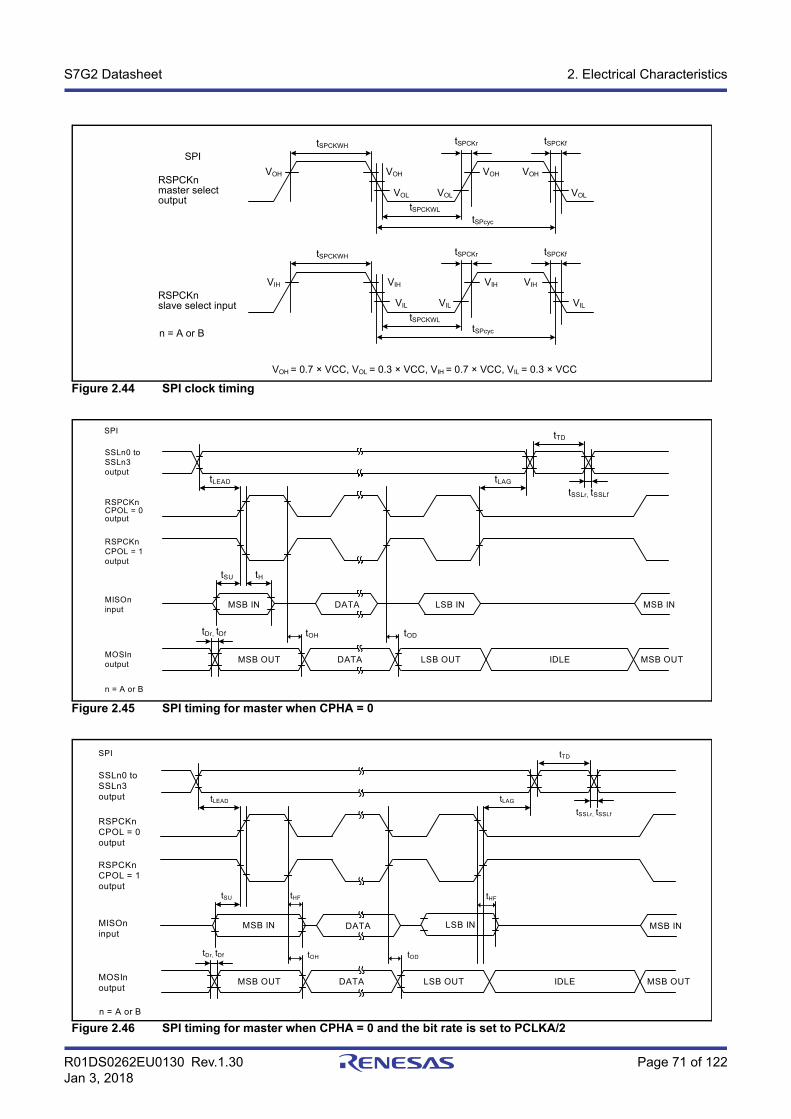
R01DS0262EU0130 Rev.1.30 Page 71 of 122Jan 3, 2018
S7G2 Datasheet 2. Electrical Characteristics
Figure 2.44 SPI clock timing
Figure 2.45 SPI timing for master when CPHA = 0
Figure 2.46 SPI timing for master when CPHA = 0 and the bit rate is set to PCLKA/2
RSPCKnmaster select output
RSPCKnslave select input
tSPCKWH
VOH VOH
VOL VOL
VOH VOH
tSPCKWL
tSPCKr tSPCKf
VOL
tSPcyc
tSPCKWH
VIH VIH
VIL VIL
VIH VIH
tSPCKWL
tSPCKr tSPCKf
VIL
tSPcyc
VOH = 0.7 × VCC, VOL = 0.3 × VCC, VIH = 0.7 × VCC, VIL = 0.3 × VCC
SPI
n = A or B
tDr, tDf
tSU tH
tLEAD
tTD
tLAG
tSSLr, tSSLf
tOH tOD
MSB IN DATA LSB IN MSB IN
MSB OUT DATA LSB OUT IDLE MSB OUT
SSLn0 to SSLn3output
RSPCKnCPOL = 0output
RSPCKnCPOL = 1output
MISOninput
MOSInoutput
SPI
n = A or B
SSLn0 to SSLn3output
RSPCKnCPOL = 0output
RSPCKnCPOL = 1output
MISOninput
MOSInoutput
LSB IN
tDr, tDf
tSU tHF
tLEAD
tTD
tLAG
tSSLr, tSSLf
tOH tOD
MSB IN
MSB OUT DATA LSB OUT IDLE MSB OUT
MSB IN DATA
tHF
SPI
n = A or B
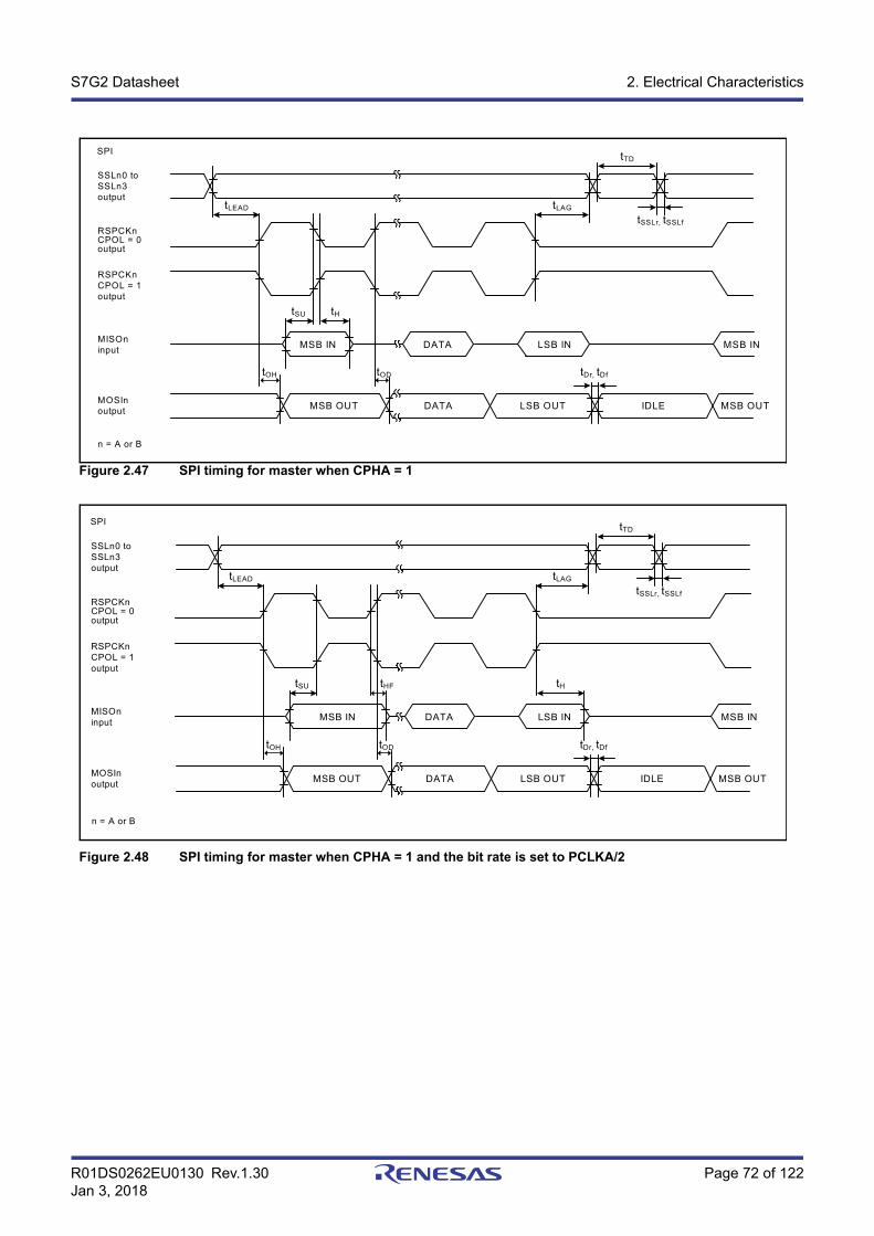
R01DS0262EU0130 Rev.1.30 Page 72 of 122Jan 3, 2018
S7G2 Datasheet 2. Electrical Characteristics
Figure 2.47 SPI timing for master when CPHA = 1
Figure 2.48 SPI timing for master when CPHA = 1 and the bit rate is set to PCLKA/2
tSU tH
tLEAD
tTD
tLAG
tSSLr, tSSLf
tOH tOD
MSB IN DATA LSB IN MSB IN
MSB OUT DATA LSB OUT IDLE MSB OUT
SSLn0 to SSLn3output
RSPCKnCPOL = 0output
RSPCKnCPOL = 1output
MISOninput
MOSInoutput
SPI
tDr, tDf
n = A or B
tSU tHF
tLEAD
tTD
tLAG
tSSLr, tSSLf
tOH tOD
MSB IN DATA LSB IN MSB IN
MSB OUT DATA LSB OUT IDLE MSB OUT
SSLn0 to SSLn3output
RSPCKnCPOL = 0output
RSPCKnCPOL = 1output
MISOninput
MOSInoutput
SPI
tDr, tDf
tH
n = A or B
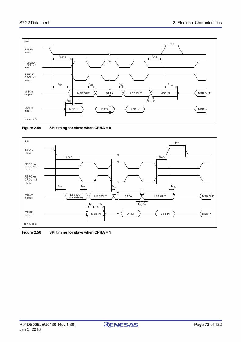
R01DS0262EU0130 Rev.1.30 Page 73 of 122Jan 3, 2018
S7G2 Datasheet 2. Electrical Characteristics
Figure 2.49 SPI timing for slave when CPHA = 0
Figure 2.50 SPI timing for slave when CPHA = 1
tDr, tDftSU tH
tLEAD
tTD
tLAG
tSA
MSB IN DATA LSB IN MSB IN
MSB OUT DATA LSB OUT MSB IN MSB OUT
tOH tOD tREL
SSLn0input
RSPCKnCPOL = 0input
RSPCKnCPOL = 1input
MISOnoutput
MOSIninput
SPI
n = A or B
SSLn0input
RSPCKnCPOL = 0input
RSPCKnCPOL = 1input
MISOnoutput
MOSIninput
tDr, tDf
tSA tOH
tLEAD
tTD
tLAG
tH
LSB OUT(Last data) DATA MSB OUT
MSB IN DATA LSB IN MSB IN
LSB OUT
tSU
tOD tREL
MSB OUT
SPI
n = A or B
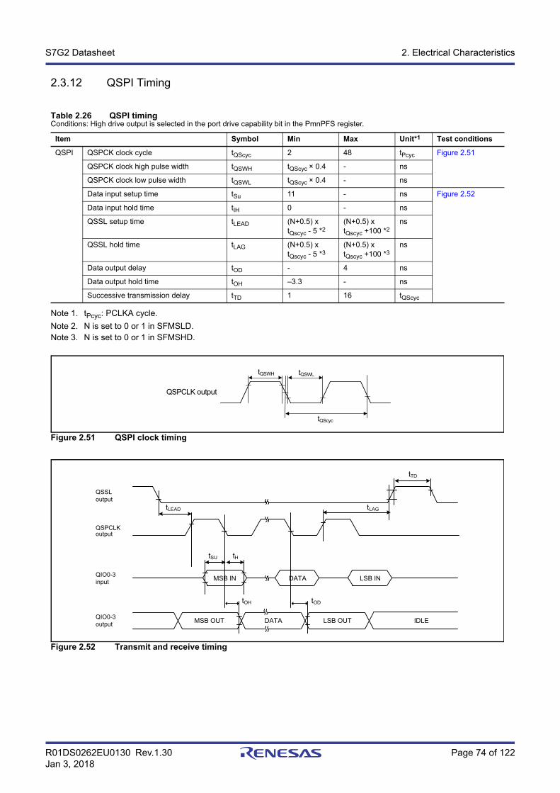
R01DS0262EU0130 Rev.1.30 Page 74 of 122Jan 3, 2018
S7G2 Datasheet 2. Electrical Characteristics
2.3.12 QSPI Timing
Note 1. tPcyc: PCLKA cycle.
Note 2. N is set to 0 or 1 in SFMSLD.Note 3. N is set to 0 or 1 in SFMSHD.
Figure 2.51 QSPI clock timing
Figure 2.52 Transmit and receive timing
Table 2.26 QSPI timingConditions: High drive output is selected in the port drive capability bit in the PmnPFS register.
Item Symbol Min Max Unit*1 Test conditions
QSPI QSPCK clock cycle tQScyc 2 48 tPcyc Figure 2.51
QSPCK clock high pulse width tQSWH tQScyc × 0.4 - ns
QSPCK clock low pulse width tQSWL tQScyc × 0.4 - ns
Data input setup time tSu 11 - ns Figure 2.52
Data input hold time tIH 0 - ns
QSSL setup time tLEAD (N+0.5) x tQscyc - 5 *2
(N+0.5) x tQscyc +100 *2
ns
QSSL hold time tLAG (N+0.5) x tQscyc - 5 *3
(N+0.5) x tQscyc +100 *3
ns
Data output delay tOD - 4 ns
Data output hold time tOH –3.3 - ns
Successive transmission delay tTD 1 16 tQScyc
tQScyc
QSPCLK output
tQSWH tQSWL
tSU tH
tLEAD
tTD
tLAG
tOH tOD
MSB IN DATA LSB IN
MSB OUT DATA LSB OUT IDLE
QSSLoutput
QSPCLKoutput
QIO0-3input
QIO0-3output
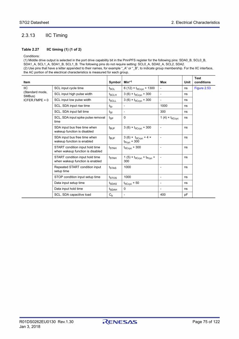
R01DS0262EU0130 Rev.1.30 Page 75 of 122Jan 3, 2018
S7G2 Datasheet 2. Electrical Characteristics
2.3.13 IIC Timing
Table 2.27 IIC timing (1) (1 of 2)
Conditions: (1) Middle drive output is selected in the port drive capability bit in the PmnPFS register for the following pins: SDA0_B, SCL0_B, SDA1_A, SCL1_A, SDA1_B, SCL1_B. The following pins do not require setting: SCL0_A, SDA0_A, SCL2, SDA2.(2) Use pins that have a letter appended to their names, for example “_A” or “_B”, to indicate group membership. For the IIC interface, the AC portion of the electrical characteristics is measured for each group.
Item Symbol Min*1 Max UnitTest conditions
IIC(Standard mode, SMBus)ICFER.FMPE = 0
SCL input cycle time tSCL 6 (12) × tIICcyc + 1300 - ns Figure 2.53
SCL input high pulse width tSCLH 3 (6) × tIICcyc + 300 - ns
SCL input low pulse width tSCLL 3 (6) × tIICcyc + 300 - ns
SCL, SDA input rise time tSr - 1000 ns
SCL, SDA input fall time tSf - 300 ns
SCL, SDA input spike pulse removal time
tSP 0 1 (4) × tIICcyc ns
SDA input bus free time when wakeup function is disabled
tBUF 3 (6) × tIICcyc + 300 - ns
SDA input bus free time when wakeup function is enabled
tBUF 3 (6) × tIICcyc + 4 × tPcyc + 300
- ns
START condition input hold time when wakeup function is disabled
tSTAH tIICcyc + 300 - ns
START condition input hold time when wakeup function is enabled
tSTAH 1 (5) × tIICcyc + tPcyc + 300
- ns
Repeated START condition input setup time
tSTAS 1000 - ns
STOP condition input setup time tSTOS 1000 - ns
Data input setup time tSDAS tIICcyc + 50 - ns
Data input hold time tSDAH 0 - ns
SCL, SDA capacitive load Cb - 400 pF
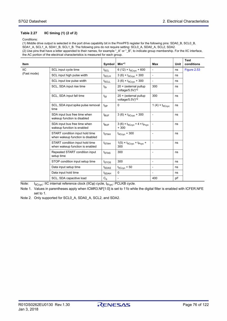
R01DS0262EU0130 Rev.1.30 Page 76 of 122Jan 3, 2018
S7G2 Datasheet 2. Electrical Characteristics
Note: tIICcyc: IIC internal reference clock (IICφ) cycle, tPcyc: PCLKB cycle.
Note 1. Values in parentheses apply when ICMR3.NF[1:0] is set to 11b while the digital filter is enabled with ICFER.NFE set to 1.
Note 2. Only supported for SCL0_A, SDA0_A, SCL2, and SDA2.
IIC(Fast mode)
SCL input cycle time tSCL 6 (12) × tIICcyc + 600 - ns Figure 2.53
SCL input high pulse width tSCLH 3 (6) × tIICcyc + 300 - ns
SCL input low pulse width tSCLL 3 (6) × tIICcyc + 300 - ns
SCL, SDA input rise time tSr 20 × (external pullup voltage/5.5V)*2
300 ns
SCL, SDA input fall time tSf 20 × (external pullup voltage/5.5V)*2
300 ns
SCL, SDA input spike pulse removal time
tSP 0 1 (4) × tIICcyc ns
SDA input bus free time when wakeup function is disabled
tBUF 3 (6) × tIICcyc + 300 - ns
SDA input bus free time when wakeup function is enabled
tBUF 3 (6) × tIICcyc + 4 × tPcyc + 300
- ns
START condition input hold time when wakeup function is disabled
tSTAH tIICcyc + 300 - ns
START condition input hold time when wakeup function is enabled
tSTAH 1(5) × tIICcyc + tPcyc + 300
- ns
Repeated START condition input setup time
tSTAS 300 - ns
STOP condition input setup time tSTOS 300 - ns
Data input setup time tSDAS tIICcyc + 50 - ns
Data input hold time tSDAH 0 - ns
SCL, SDA capacitive load Cb - 400 pF
Table 2.27 IIC timing (1) (2 of 2)
Conditions: (1) Middle drive output is selected in the port drive capability bit in the PmnPFS register for the following pins: SDA0_B, SCL0_B, SDA1_A, SCL1_A, SDA1_B, SCL1_B. The following pins do not require setting: SCL0_A, SDA0_A, SCL2, SDA2.(2) Use pins that have a letter appended to their names, for example “_A” or “_B”, to indicate group membership. For the IIC interface, the AC portion of the electrical characteristics is measured for each group.
Item Symbol Min*1 Max UnitTest conditions
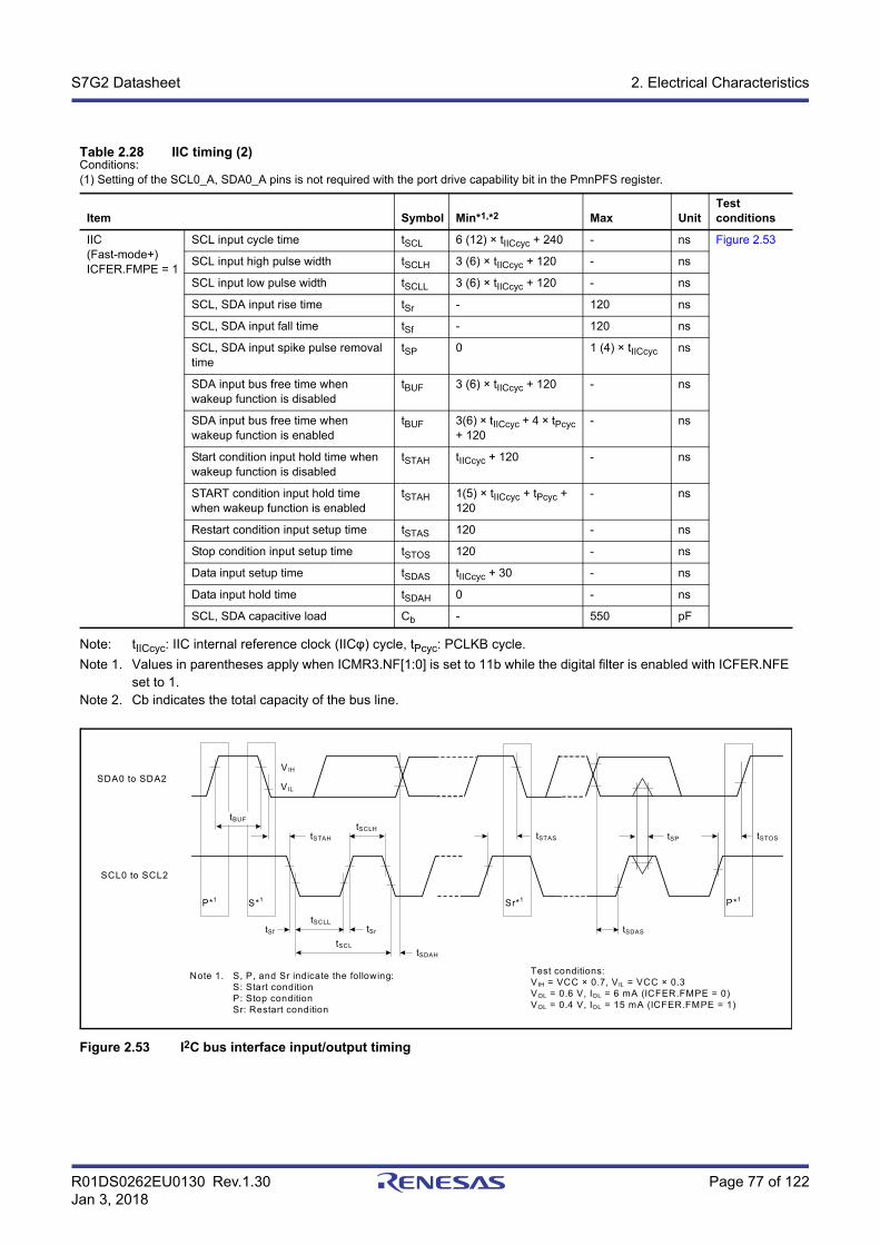
R01DS0262EU0130 Rev.1.30 Page 77 of 122Jan 3, 2018
S7G2 Datasheet 2. Electrical Characteristics
Note: tIICcyc: IIC internal reference clock (IICφ) cycle, tPcyc: PCLKB cycle.
Note 1. Values in parentheses apply when ICMR3.NF[1:0] is set to 11b while the digital filter is enabled with ICFER.NFE set to 1.
Note 2. Cb indicates the total capacity of the bus line.
Figure 2.53 I2C bus interface input/output timing
Table 2.28 IIC timing (2)Conditions:(1) Setting of the SCL0_A, SDA0_A pins is not required with the port drive capability bit in the PmnPFS register.
Item Symbol Min*1,*2 Max UnitTest conditions
IIC(Fast-mode+) ICFER.FMPE = 1
SCL input cycle time tSCL 6 (12) × tIICcyc + 240 - ns Figure 2.53
SCL input high pulse width tSCLH 3 (6) × tIICcyc + 120 - ns
SCL input low pulse width tSCLL 3 (6) × tIICcyc + 120 - ns
SCL, SDA input rise time tSr - 120 ns
SCL, SDA input fall time tSf - 120 ns
SCL, SDA input spike pulse removal time
tSP 0 1 (4) × tIICcyc ns
SDA input bus free time when wakeup function is disabled
tBUF 3 (6) × tIICcyc + 120 - ns
SDA input bus free time when wakeup function is enabled
tBUF 3(6) × tIICcyc + 4 × tPcyc + 120
- ns
Start condition input hold time when wakeup function is disabled
tSTAH tIICcyc + 120 - ns
START condition input hold time when wakeup function is enabled
tSTAH 1(5) × tIICcyc + tPcyc + 120
- ns
Restart condition input setup time tSTAS 120 - ns
Stop condition input setup time tSTOS 120 - ns
Data input setup time tSDAS tIICcyc + 30 - ns
Data input hold time tSDAH 0 - ns
SCL, SDA capacitive load Cb - 550 pF
SDA0 to SDA2
SCL0 to SCL2
VIH
VIL
tSTAH
tSCLH
tSCLL
P*1 S*1
tSf tSr
tSCLtSDAH
tSDAS
tSTAS tSP tSTOS
P*1
tBUF
Test conditions:VIH = VCC × 0.7, VIL = VCC × 0.3VOL = 0.6 V, IOL = 6 mA (ICFER.FMPE = 0)VOL = 0.4 V, IOL = 15 mA (ICFER.FMPE = 1)
Sr*1
Note 1. S, P, and Sr indicate the following:S: Start conditionP: Stop conditionSr: Restart condition
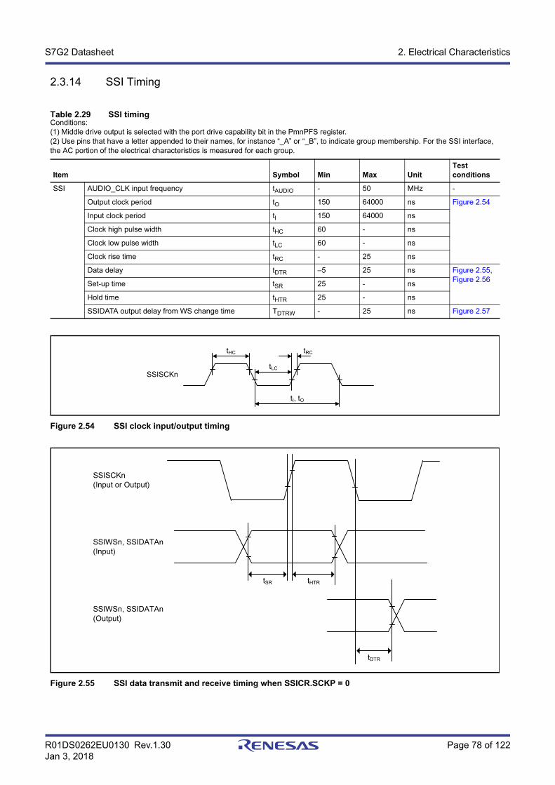
R01DS0262EU0130 Rev.1.30 Page 78 of 122Jan 3, 2018
S7G2 Datasheet 2. Electrical Characteristics
2.3.14 SSI Timing
Figure 2.54 SSI clock input/output timing
Figure 2.55 SSI data transmit and receive timing when SSICR.SCKP = 0
Table 2.29 SSI timingConditions:(1) Middle drive output is selected with the port drive capability bit in the PmnPFS register.(2) Use pins that have a letter appended to their names, for instance “_A” or “_B”, to indicate group membership. For the SSI interface, the AC portion of the electrical characteristics is measured for each group.
Item Symbol Min Max UnitTest conditions
SSI AUDIO_CLK input frequency tAUDIO - 50 MHz -
Output clock period tO 150 64000 ns Figure 2.54
Input clock period tI 150 64000 ns
Clock high pulse width tHC 60 - ns
Clock low pulse width tLC 60 - ns
Clock rise time tRC - 25 ns
Data delay tDTR –5 25 ns Figure 2.55, Figure 2.56
Set-up time tSR 25 - ns
Hold time tHTR 25 - ns
SSIDATA output delay from WS change time TDTRW - 25 ns Figure 2.57
SSISCKn
tHC
tLC
tRC
tI, tO
tSR tHTR
tDTR
SSISCKn(Input or Output)
SSIWSn, SSIDATAn(Input)
SSIWSn, SSIDATAn(Output)
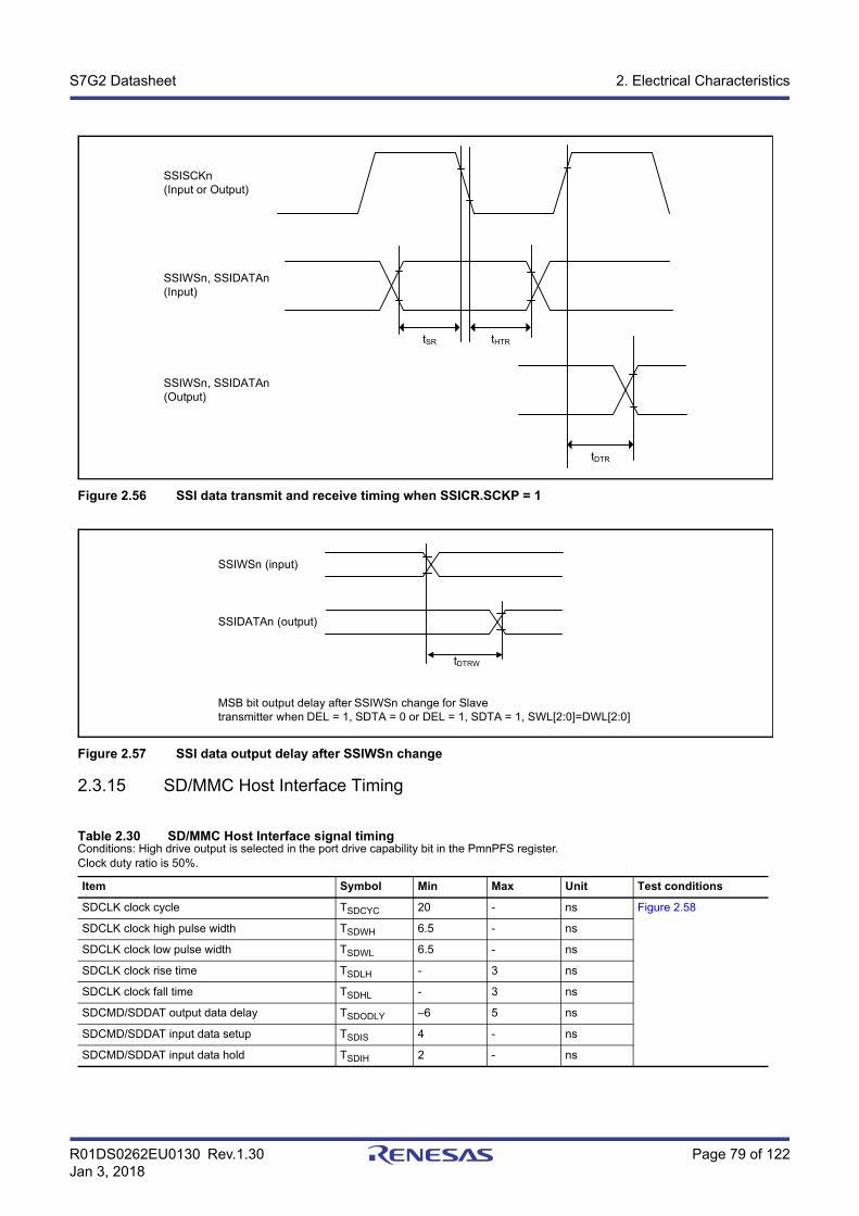
R01DS0262EU0130 Rev.1.30 Page 79 of 122Jan 3, 2018
S7G2 Datasheet 2. Electrical Characteristics
Figure 2.56 SSI data transmit and receive timing when SSICR.SCKP = 1
Figure 2.57 SSI data output delay after SSIWSn change
2.3.15 SD/MMC Host Interface Timing
Table 2.30 SD/MMC Host Interface signal timingConditions: High drive output is selected in the port drive capability bit in the PmnPFS register.Clock duty ratio is 50%.
Item Symbol Min Max Unit Test conditions
SDCLK clock cycle TSDCYC 20 - ns Figure 2.58
SDCLK clock high pulse width TSDWH 6.5 - ns
SDCLK clock low pulse width TSDWL 6.5 - ns
SDCLK clock rise time TSDLH - 3 ns
SDCLK clock fall time TSDHL - 3 ns
SDCMD/SDDAT output data delay TSDODLY –6 5 ns
SDCMD/SDDAT input data setup TSDIS 4 - ns
SDCMD/SDDAT input data hold TSDIH 2 - ns
tSR tHTR
tDTR
SSISCKn(Input or Output)
SSIWSn, SSIDATAn(Input)
SSIWSn, SSIDATAn(Output)
tDTRW
SSIWSn (input)
SSIDATAn (output)
MSB bit output delay after SSIWSn change for Slavetransmitter when DEL = 1, SDTA = 0 or DEL = 1, SDTA = 1, SWL[2:0]=DWL[2:0]
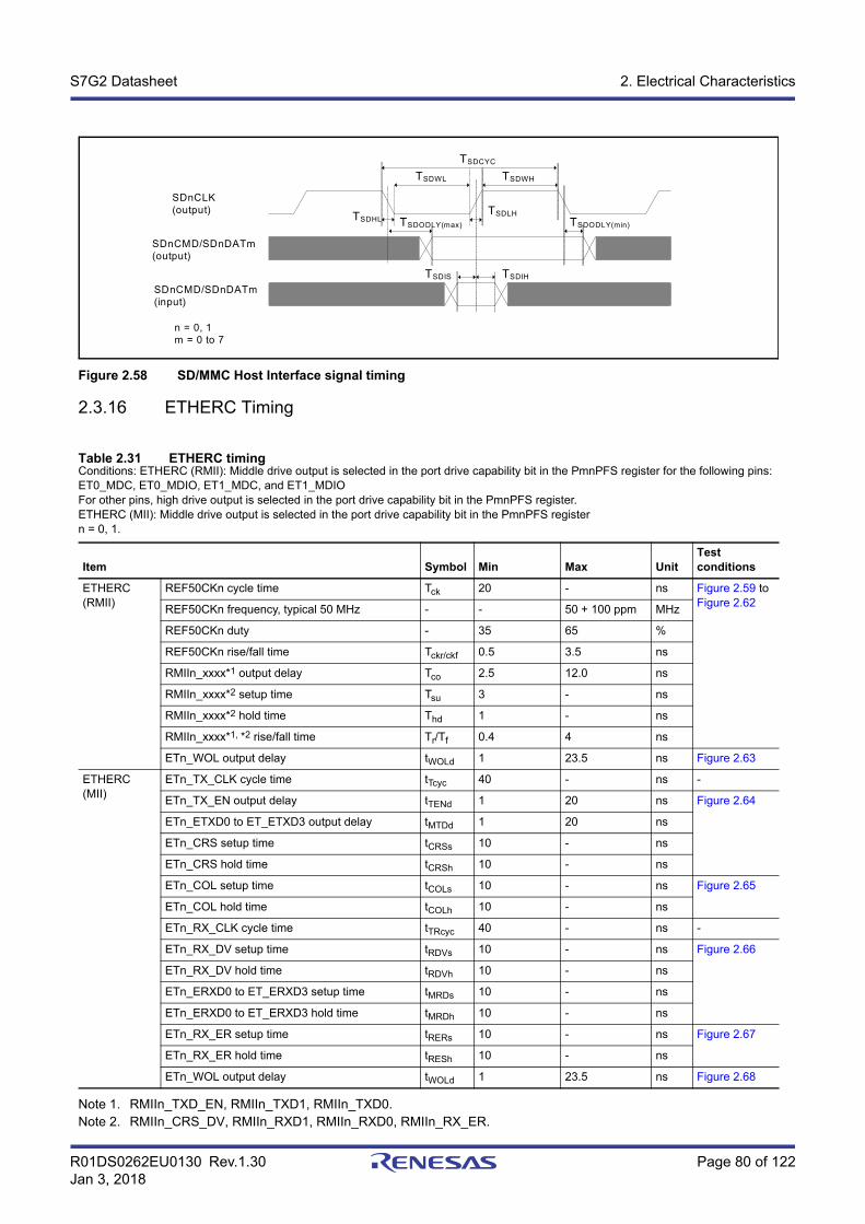
R01DS0262EU0130 Rev.1.30 Page 80 of 122Jan 3, 2018
S7G2 Datasheet 2. Electrical Characteristics
Figure 2.58 SD/MMC Host Interface signal timing
2.3.16 ETHERC Timing
Note 1. RMIIn_TXD_EN, RMIIn_TXD1, RMIIn_TXD0.Note 2. RMIIn_CRS_DV, RMIIn_RXD1, RMIIn_RXD0, RMIIn_RX_ER.
Table 2.31 ETHERC timingConditions: ETHERC (RMII): Middle drive output is selected in the port drive capability bit in the PmnPFS register for the following pins: ET0_MDC, ET0_MDIO, ET1_MDC, and ET1_MDIOFor other pins, high drive output is selected in the port drive capability bit in the PmnPFS register.ETHERC (MII): Middle drive output is selected in the port drive capability bit in the PmnPFS registern = 0, 1.
Item Symbol Min Max UnitTest conditions
ETHERC (RMII)
REF50CKn cycle time Tck 20 - ns Figure 2.59 to Figure 2.62
REF50CKn frequency, typical 50 MHz - - 50 + 100 ppm MHz
REF50CKn duty - 35 65 %
REF50CKn rise/fall time Tckr/ckf 0.5 3.5 ns
RMIIn_xxxx*1 output delay Tco 2.5 12.0 ns
RMIIn_xxxx*2 setup time Tsu 3 - ns
RMIIn_xxxx*2 hold time Thd 1 - ns
RMIIn_xxxx*1, *2 rise/fall time Tr/Tf 0.4 4 ns
ETn_WOL output delay tWOLd 1 23.5 ns Figure 2.63
ETHERC (MII)
ETn_TX_CLK cycle time tTcyc 40 - ns -
ETn_TX_EN output delay tTENd 1 20 ns Figure 2.64
ETn_ETXD0 to ET_ETXD3 output delay tMTDd 1 20 ns
ETn_CRS setup time tCRSs 10 - ns
ETn_CRS hold time tCRSh 10 - ns
ETn_COL setup time tCOLs 10 - ns Figure 2.65
ETn_COL hold time tCOLh 10 - ns
ETn_RX_CLK cycle time tTRcyc 40 - ns -
ETn_RX_DV setup time tRDVs 10 - ns Figure 2.66
ETn_RX_DV hold time tRDVh 10 - ns
ETn_ERXD0 to ET_ERXD3 setup time tMRDs 10 - ns
ETn_ERXD0 to ET_ERXD3 hold time tMRDh 10 - ns
ETn_RX_ER setup time tRERs 10 - ns Figure 2.67
ETn_RX_ER hold time tRESh 10 - ns
ETn_WOL output delay tWOLd 1 23.5 ns Figure 2.68
SDnCLK(output)
SDnCMD/SDnDATm(input)
SDnCMD/SDnDATm(output)
TSDODLY(max)
TSDIS TSDIH
TSDLHTSDHL
TSDCYC
TSDWHTSDWL
TSDODLY(min)
n = 0, 1 m = 0 to 7
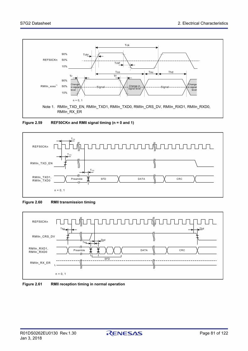
R01DS0262EU0130 Rev.1.30 Page 81 of 122Jan 3, 2018
S7G2 Datasheet 2. Electrical Characteristics
Figure 2.59 REF50CKn and RMII signal timing (n = 0 and 1)
Figure 2.60 RMII transmission timing
Figure 2.61 RMII reception timing in normal operation
Note 1. RMIIn_TXD_EN, RMIIn_TXD1, RMIIn_TXD0, RMIIn_CRS_DV, RMIIn_RXD1, RMIIn_RXD0, RMIIn_RX_ER
Change in signal level
Signal
ThdTsuTco
TfTr
Tckr
Tckf
Tck
Signal
90%
50%
10%
90%
50%
REF50CKn
RMIIn_xxxx*1
10%
Change in signal level
Change in signal
level
n = 0, 1
Preamble SFD DATA CRC
TCO
TCO
TCK
REF50CKn
RMIIn_TXD_EN
RMIIn_TXD1,RMIIn_TXD0
n = 0, 1
Preamble DATA CRC
SFD
Tsu
TsuThd
Thd
L
REF50CKn
RMIIn_CRS_DV
RMIIn_RXD1,RMIIn_RXD0
RMIIn_RX_ER
n = 0, 1
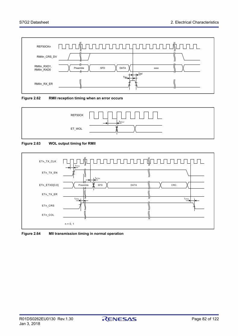
R01DS0262EU0130 Rev.1.30 Page 82 of 122Jan 3, 2018
S7G2 Datasheet 2. Electrical Characteristics
Figure 2.62 RMII reception timing when an error occurs
Figure 2.63 WOL output timing for RMII
Figure 2.64 MII transmission timing in normal operation
Preamble DATA
REF50CKn
RMIIn_CRS_DV
RMIIn_RXD1,RMIIn_RXD0
SFD xxxx
RMIIn_RX_ER
Tsu
Thd
tWOLd
REF50CK
ET_WOL
ETn_TX_CLK
ETn_TX_EN
ETn_ETXD[3:0]
ETn_TX_ER
ETn_CRS
ETn_COL
SFD DATA CRCPreamble
tTENd
tMTDd
tCRSs tCRSh
n = 0, 1
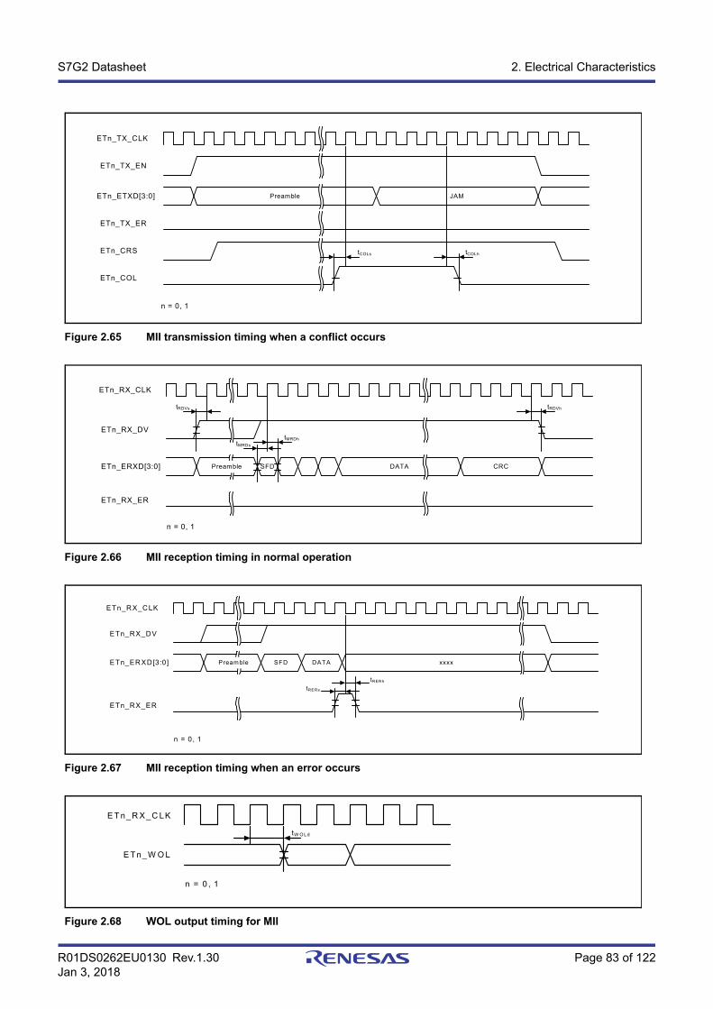
R01DS0262EU0130 Rev.1.30 Page 83 of 122Jan 3, 2018
S7G2 Datasheet 2. Electrical Characteristics
Figure 2.65 MII transmission timing when a conflict occurs
Figure 2.66 MII reception timing in normal operation
Figure 2.67 MII reception timing when an error occurs
Figure 2.68 WOL output timing for MII
ETn_TX_CLK
ETn_TX_EN
ETn_ETXD[3:0]
ETn_TX_ER
ETn_CRS
ETn_COL
JAMPreamble
tCOLs tCOLh
n = 0, 1
Preamble DATA CRCSFD
tRDVs
tMRDs
tMRDh
tRDVh
ETn_RX_CLK
ETn_RX_DV
ETn_ERXD[3:0]
ETn_RX_ER
n = 0, 1
Pream ble DATASFD
tRERs
ETn_R X_C LK
ETn_RX_DV
ETn_ER XD[3:0]
ETn_RX_ER
xxxx
tRERh
n = 0, 1
tW O Ld
E T n_R X _C LK
E T n_W O L
n = 0 , 1
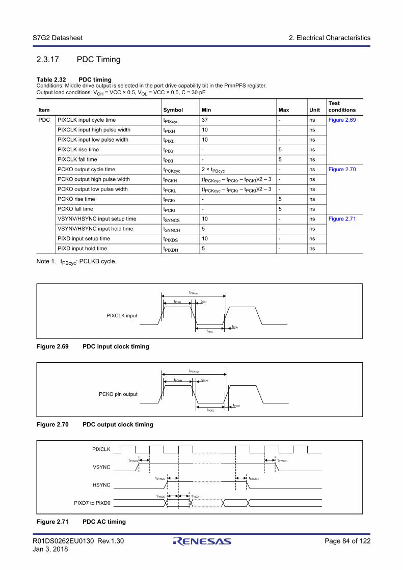
R01DS0262EU0130 Rev.1.30 Page 84 of 122Jan 3, 2018
S7G2 Datasheet 2. Electrical Characteristics
2.3.17 PDC Timing
Note 1. tPBcyc: PCLKB cycle.
Figure 2.69 PDC input clock timing
Figure 2.70 PDC output clock timing
Figure 2.71 PDC AC timing
Table 2.32 PDC timingConditions: Middle drive output is selected in the port drive capability bit in the PmnPFS register.Output load conditions: VOH = VCC × 0.5, VOL = VCC × 0.5, C = 30 pF
Item Symbol Min Max UnitTest conditions
PDC PIXCLK input cycle time tPIXcyc 37 - ns Figure 2.69
PIXCLK input high pulse width tPIXH 10 - ns
PIXCLK input low pulse width tPIXL 10 - ns
PIXCLK rise time tPIXr - 5 ns
PIXCLK fall time tPIXf - 5 ns
PCKO output cycle time tPCKcyc 2 × tPBcyc - ns Figure 2.70
PCKO output high pulse width tPCKH (tPCKcyc – tPCKr – tPCKf)/2 – 3 - ns
PCKO output low pulse width tPCKL (tPCKcyc – tPCKr – tPCKf)/2 – 3 - ns
PCKO rise time tPCKr - 5 ns
PCKO fall time tPCKf - 5 ns
VSYNV/HSYNC input setup time tSYNCS 10 - ns Figure 2.71
VSYNV/HSYNC input hold time tSYNCH 5 - ns
PIXD input setup time tPIXDS 10 - ns
PIXD input hold time tPIXDH 5 - ns
tPIXcyc
tPIXH tPIXf
tPIXL
tPIXr
PIXCLK input
tPCKcyc
tPCKH tPCKf
tPCKL
tPCKr
PCKO pin output
PIXCLK
VSYNC
HSYNC
PIXD7 to PIXD0
tSYNCS
tSYNCS
tPIXDS tPIXDH
tSYNCH
tSYNCH
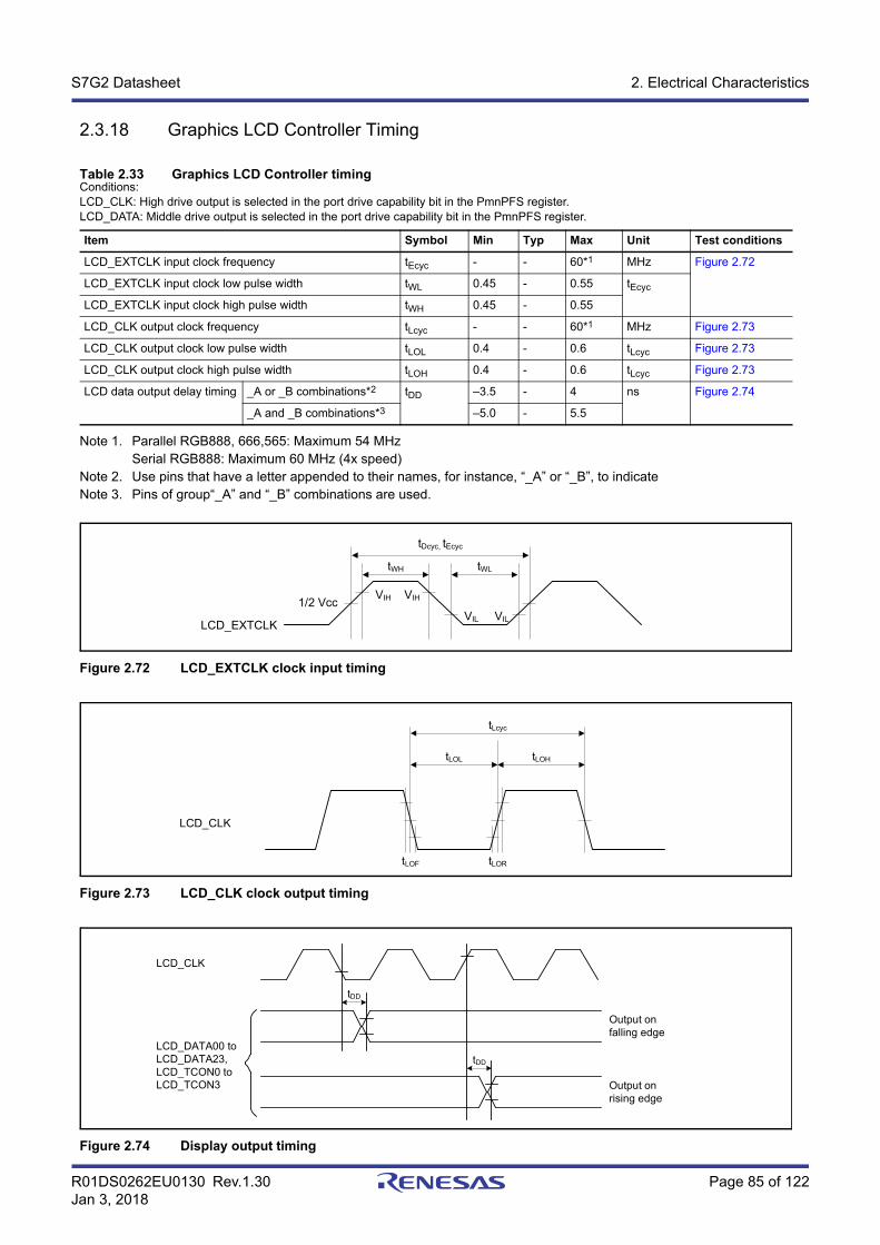
R01DS0262EU0130 Rev.1.30 Page 85 of 122Jan 3, 2018
S7G2 Datasheet 2. Electrical Characteristics
2.3.18 Graphics LCD Controller Timing
Note 1. Parallel RGB888, 666,565: Maximum 54 MHzSerial RGB888: Maximum 60 MHz (4x speed)
Note 2. Use pins that have a letter appended to their names, for instance, “_A” or “_B”, to indicateNote 3. Pins of group“_A” and “_B” combinations are used.
Figure 2.72 LCD_EXTCLK clock input timing
Figure 2.73 LCD_CLK clock output timing
Figure 2.74 Display output timing
Table 2.33 Graphics LCD Controller timingConditions:LCD_CLK: High drive output is selected in the port drive capability bit in the PmnPFS register.LCD_DATA: Middle drive output is selected in the port drive capability bit in the PmnPFS register.
Item Symbol Min Typ Max Unit Test conditions
LCD_EXTCLK input clock frequency tEcyc - - 60*1 MHz Figure 2.72
LCD_EXTCLK input clock low pulse width tWL 0.45 - 0.55 tEcyc
LCD_EXTCLK input clock high pulse width tWH 0.45 - 0.55
LCD_CLK output clock frequency tLcyc - - 60*1 MHz Figure 2.73
LCD_CLK output clock low pulse width tLOL 0.4 - 0.6 tLcyc Figure 2.73
LCD_CLK output clock high pulse width tLOH 0.4 - 0.6 tLcyc Figure 2.73
LCD data output delay timing _A or _B combinations*2 tDD –3.5 - 4 ns Figure 2.74
_A and _B combinations*3 –5.0 - 5.5
1/2 VccVIH VIH
VIL VIL
tDcyc, tEcyc
tWH tWL
LCD_EXTCLK
tLcyc
tLOL tLOH
tLOF tLOR
LCD_CLK
LCD_CLK
tDD
tDD
LCD_DATA00 to LCD_DATA23,LCD_TCON0 to LCD_TCON3
Output on falling edge
Output on rising edge
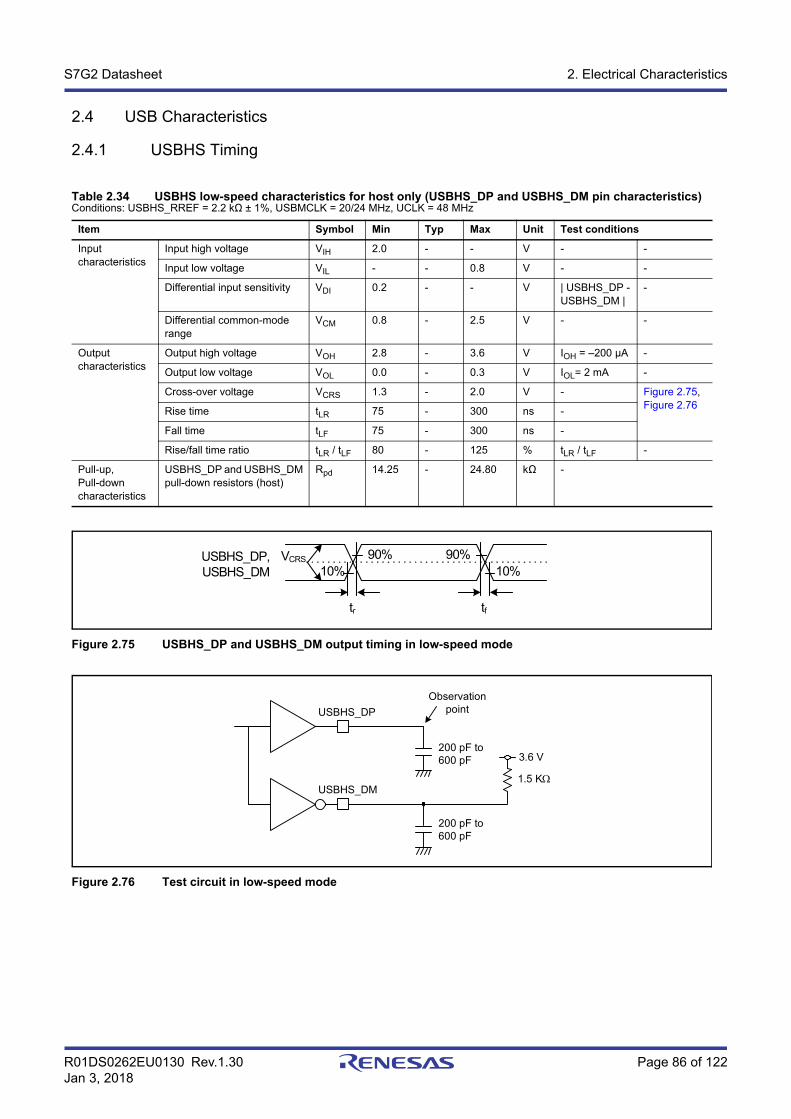
R01DS0262EU0130 Rev.1.30 Page 86 of 122Jan 3, 2018
S7G2 Datasheet 2. Electrical Characteristics
2.4 USB Characteristics
2.4.1 USBHS Timing
Figure 2.75 USBHS_DP and USBHS_DM output timing in low-speed mode
Figure 2.76 Test circuit in low-speed mode
Table 2.34 USBHS low-speed characteristics for host only (USBHS_DP and USBHS_DM pin characteristics)Conditions: USBHS_RREF = 2.2 kΩ ± 1%, USBMCLK = 20/24 MHz, UCLK = 48 MHz
Item Symbol Min Typ Max Unit Test conditions
Input characteristics
Input high voltage VIH 2.0 - - V - -
Input low voltage VIL - - 0.8 V - -
Differential input sensitivity VDI 0.2 - - V | USBHS_DP - USBHS_DM |
-
Differential common-mode range
VCM 0.8 - 2.5 V - -
Output characteristics
Output high voltage VOH 2.8 - 3.6 V IOH = –200 μA -
Output low voltage VOL 0.0 - 0.3 V IOL= 2 mA -
Cross-over voltage VCRS 1.3 - 2.0 V - Figure 2.75, Figure 2.76
Rise time tLR 75 - 300 ns -
Fall time tLF 75 - 300 ns -
Rise/fall time ratio tLR / tLF 80 - 125 % tLR / tLF -
Pull-up, Pull-down characteristics
USBHS_DP and USBHS_DM pull-down resistors (host)
Rpd 14.25 - 24.80 kΩ -
USBHS_DP, USBHS_DM
tftr
90%10%10%
90%VCRS
Observation point
200 pF to 600 pF
USBHS_DP
USBHS_DM
200 pF to 600 pF
1.5 K
3.6 V
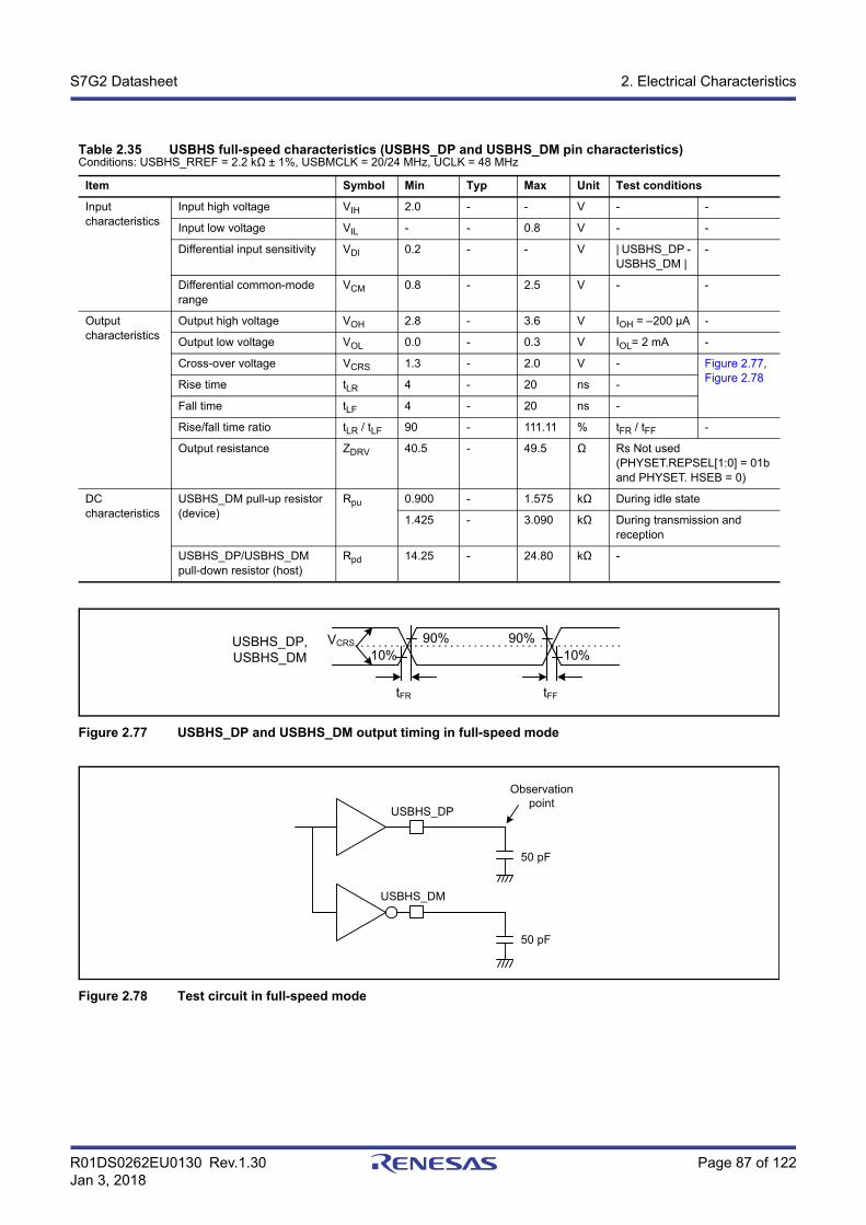
R01DS0262EU0130 Rev.1.30 Page 87 of 122Jan 3, 2018
S7G2 Datasheet 2. Electrical Characteristics
Figure 2.77 USBHS_DP and USBHS_DM output timing in full-speed mode
Figure 2.78 Test circuit in full-speed mode
Table 2.35 USBHS full-speed characteristics (USBHS_DP and USBHS_DM pin characteristics)Conditions: USBHS_RREF = 2.2 kΩ ± 1%, USBMCLK = 20/24 MHz, UCLK = 48 MHz
Item Symbol Min Typ Max Unit Test conditions
Input characteristics
Input high voltage VIH 2.0 - - V - -
Input low voltage VIL - - 0.8 V - -
Differential input sensitivity VDI 0.2 - - V | USBHS_DP - USBHS_DM |
-
Differential common-mode range
VCM 0.8 - 2.5 V - -
Output characteristics
Output high voltage VOH 2.8 - 3.6 V IOH = –200 μA -
Output low voltage VOL 0.0 - 0.3 V IOL= 2 mA -
Cross-over voltage VCRS 1.3 - 2.0 V - Figure 2.77, Figure 2.78
Rise time tLR 4 - 20 ns -
Fall time tLF 4 - 20 ns -
Rise/fall time ratio tLR / tLF 90 - 111.11 % tFR / tFF -
Output resistance ZDRV 40.5 - 49.5 Ω Rs Not used(PHYSET.REPSEL[1:0] = 01b and PHYSET. HSEB = 0)
DC characteristics
USBHS_DM pull-up resistor (device)
Rpu 0.900 - 1.575 kΩ During idle state
1.425 - 3.090 kΩ During transmission and reception
USBHS_DP/USBHS_DM pull-down resistor (host)
Rpd 14.25 - 24.80 kΩ -
USBHS_DP,USBHS_DM
tFFtFR
90%10%10%
90%VCRS
Observation point
50 pF
50 pF
USBHS_DP
USBHS_DM
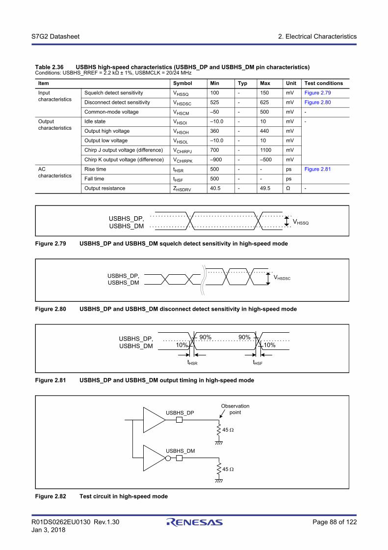
R01DS0262EU0130 Rev.1.30 Page 88 of 122Jan 3, 2018
S7G2 Datasheet 2. Electrical Characteristics
Figure 2.79 USBHS_DP and USBHS_DM squelch detect sensitivity in high-speed mode
Figure 2.80 USBHS_DP and USBHS_DM disconnect detect sensitivity in high-speed mode
Figure 2.81 USBHS_DP and USBHS_DM output timing in high-speed mode
Figure 2.82 Test circuit in high-speed mode
Table 2.36 USBHS high-speed characteristics (USBHS_DP and USBHS_DM pin characteristics)Conditions: USBHS_RREF = 2.2 kΩ ± 1%, USBMCLK = 20/24 MHz
Item Symbol Min Typ Max Unit Test conditions
Input characteristics
Squelch detect sensitivity VHSSQ 100 - 150 mV Figure 2.79
Disconnect detect sensitivity VHSDSC 525 - 625 mV Figure 2.80
Common-mode voltage VHSCM –50 - 500 mV -
Output characteristics
Idle state VHSOI –10.0 - 10 mV -
Output high voltage VHSOH 360 - 440 mV
Output low voltage VHSOL –10.0 - 10 mV
Chirp J output voltage (difference) VCHIRPJ 700 - 1100 mV
Chirp K output voltage (difference) VCHIRPK –900 - –500 mV
AC characteristics
Rise time tHSR 500 - - ps Figure 2.81
Fall time tHSF 500 - - ps
Output resistance ZHSDRV 40.5 - 49.5 Ω -
USBHS_DP,USBHS_DM
VHSSQ
USBHS_DP,USBHS_DM
VHSDSC
USBHS_DP,USBHS_DM
tHSFtHSR
90%10%10%
90%
Observation pointUSBHS_DP
USBHS_DM
45
45
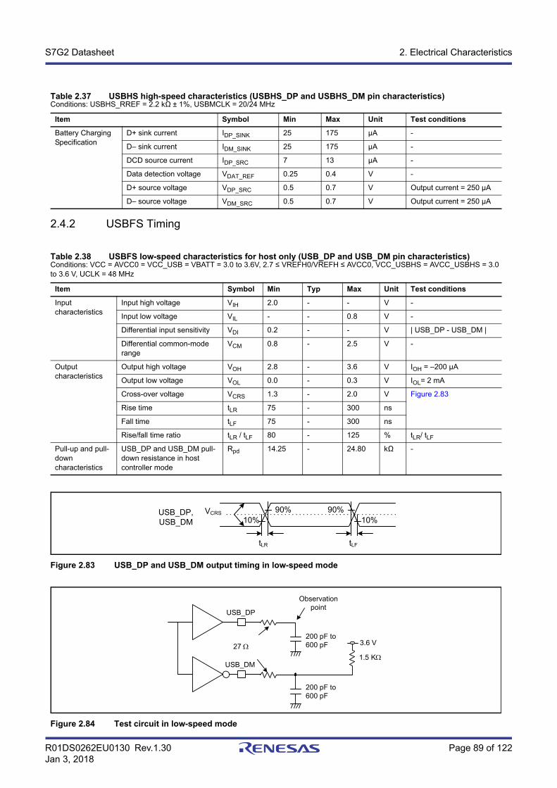
R01DS0262EU0130 Rev.1.30 Page 89 of 122Jan 3, 2018
S7G2 Datasheet 2. Electrical Characteristics
2.4.2 USBFS Timing
Figure 2.83 USB_DP and USB_DM output timing in low-speed mode
Figure 2.84 Test circuit in low-speed mode
Table 2.37 USBHS high-speed characteristics (USBHS_DP and USBHS_DM pin characteristics)Conditions: USBHS_RREF = 2.2 kΩ ± 1%, USBMCLK = 20/24 MHz
Item Symbol Min Max Unit Test conditions
Battery Charging Specification
D+ sink current IDP_SINK 25 175 μA -
D– sink current IDM_SINK 25 175 μA -
DCD source current IDP_SRC 7 13 μA -
Data detection voltage VDAT_REF 0.25 0.4 V -
D+ source voltage VDP_SRC 0.5 0.7 V Output current = 250 μA
D– source voltage VDM_SRC 0.5 0.7 V Output current = 250 μA
Table 2.38 USBFS low-speed characteristics for host only (USB_DP and USB_DM pin characteristics)Conditions: VCC = AVCC0 = VCC_USB = VBATT = 3.0 to 3.6V, 2.7 ≤ VREFH0/VREFH ≤ AVCC0, VCC_USBHS = AVCC_USBHS = 3.0 to 3.6 V, UCLK = 48 MHz
Item Symbol Min Typ Max Unit Test conditions
Input characteristics
Input high voltage VIH 2.0 - - V -
Input low voltage VIL - - 0.8 V -
Differential input sensitivity VDI 0.2 - - V | USB_DP - USB_DM |
Differential common-mode range
VCM 0.8 - 2.5 V -
Output characteristics
Output high voltage VOH 2.8 - 3.6 V IOH = –200 μA
Output low voltage VOL 0.0 - 0.3 V IOL= 2 mA
Cross-over voltage VCRS 1.3 - 2.0 V Figure 2.83
Rise time tLR 75 - 300 ns
Fall time tLF 75 - 300 ns
Rise/fall time ratio tLR / tLF 80 - 125 % tLR/ tLF
Pull-up and pull-down characteristics
USB_DP and USB_DM pull-down resistance in host controller mode
Rpd 14.25 - 24.80 kΩ -
USB_DP,USB_DM
tLFtLR
90%10%10%
90%VCRS
Observation point
200 pF to 600 pF
USB_DP
USB_DM
200 pF to 600 pF
1.5 K
3.6 V27
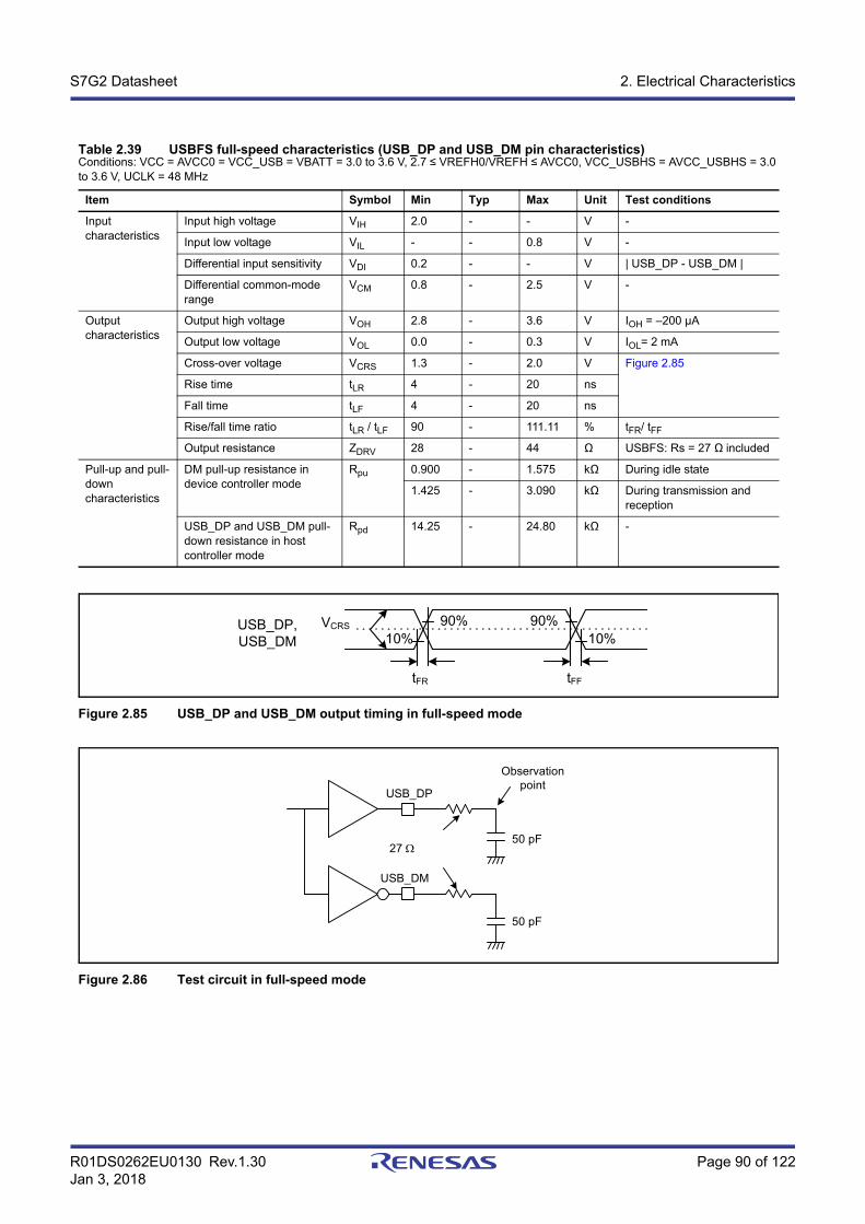
R01DS0262EU0130 Rev.1.30 Page 90 of 122Jan 3, 2018
S7G2 Datasheet 2. Electrical Characteristics
Figure 2.85 USB_DP and USB_DM output timing in full-speed mode
Figure 2.86 Test circuit in full-speed mode
Table 2.39 USBFS full-speed characteristics (USB_DP and USB_DM pin characteristics)Conditions: VCC = AVCC0 = VCC_USB = VBATT = 3.0 to 3.6 V, 2.7 ≤ VREFH0/VREFH ≤ AVCC0, VCC_USBHS = AVCC_USBHS = 3.0 to 3.6 V, UCLK = 48 MHz
Item Symbol Min Typ Max Unit Test conditions
Input characteristics
Input high voltage VIH 2.0 - - V -
Input low voltage VIL - - 0.8 V -
Differential input sensitivity VDI 0.2 - - V | USB_DP - USB_DM |
Differential common-mode range
VCM 0.8 - 2.5 V -
Output characteristics
Output high voltage VOH 2.8 - 3.6 V IOH = –200 μA
Output low voltage VOL 0.0 - 0.3 V IOL= 2 mA
Cross-over voltage VCRS 1.3 - 2.0 V Figure 2.85
Rise time tLR 4 - 20 ns
Fall time tLF 4 - 20 ns
Rise/fall time ratio tLR / tLF 90 - 111.11 % tFR/ tFF
Output resistance ZDRV 28 - 44 Ω USBFS: Rs = 27 Ω included
Pull-up and pull-down characteristics
DM pull-up resistance in device controller mode
Rpu 0.900 - 1.575 kΩ During idle state
1.425 - 3.090 kΩ During transmission and reception
USB_DP and USB_DM pull-down resistance in host controller mode
Rpd 14.25 - 24.80 kΩ -
USB_DP,USB_DM
tFFtFR
90%10%10%
90%VCRS
Observation point
50 pF
50 pF
USB_DP
USB_DM
27
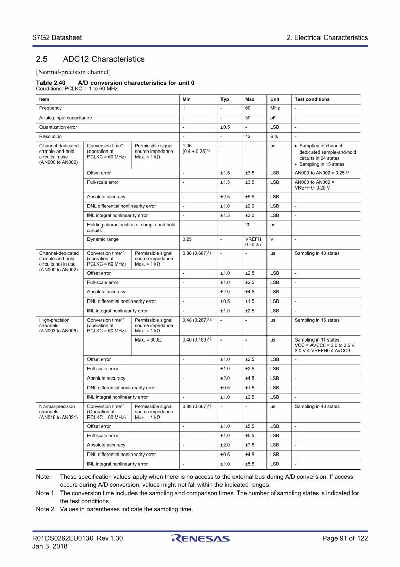
R01DS0262EU0130 Rev.1.30 Page 91 of 122Jan 3, 2018
S7G2 Datasheet 2. Electrical Characteristics
2.5 ADC12 Characteristics
[Normal-precision channel]
Note: These specification values apply when there is no access to the external bus during A/D conversion. If access occurs during A/D conversion, values might not fall within the indicated ranges.
Note 1. The conversion time includes the sampling and comparison times. The number of sampling states is indicated for the test conditions.
Note 2. Values in parentheses indicate the sampling time.
Table 2.40 A/D conversion characteristics for unit 0Conditions: PCLKC = 1 to 60 MHz
Item Min Typ Max Unit Test conditions
Frequency 1 - 60 MHz -
Analog input capacitance - - 30 pF -
Quantization error - ±0.5 - LSB -
Resolution - - 12 Bits -
Channel-dedicated sample-and-hold circuits in use (AN000 to AN002)
Conversion time*1 (operation at PCLKC = 60 MHz)
Permissible signal source impedance Max. = 1 kΩ
1.06 (0.4 + 0.25)*2
- - μs Sampling of channel-dedicated sample-and-hold circuits in 24 states
Sampling in 15 states
Offset error - ±1.5 ±3.5 LSB AN000 to AN002 = 0.25 V
Full-scale error - ±1.5 ±3.5 LSB AN000 to AN002 = VREFH0- 0.25 V
Absolute accuracy - ±2.5 ±5.5 LSB -
DNL differential nonlinearity error - ±1.0 ±2.0 LSB -
INL integral nonlinearity error - ±1.5 ±3.0 LSB -
Holding characteristics of sample-and hold circuits
- - 20 μs -
Dynamic range 0.25 - VREFH0 –0.25
V -
Channel-dedicated sample-and-hold circuits not in use (AN000 to AN002)
Conversion time*1 (operation at PCLKC = 60 MHz)
Permissible signal source impedance Max. = 1 kΩ
0.88 (0.667)*2 - - μs Sampling in 40 states
Offset error - ±1.0 ±2.5 LSB -
Full-scale error - ±1.0 ±2.5 LSB -
Absolute accuracy - ±2.0 ±4.5 LSB -
DNL differential nonlinearity error - ±0.5 ±1.5 LSB -
INL integral nonlinearity error - ±1.0 ±2.5 LSB -
High-precision channels(AN003 to AN006)
Conversion time*1
(operation at PCLKC = 60 MHz)
Permissible signal source impedance Max. = 1 kΩ
0.48 (0.267)*2 - - μs Sampling in 16 states
Max. = 300Ω 0.40 (0.183)*2 - - μs Sampling in 11 statesVCC = AVCC0 = 3.0 to 3.6 V3.0 V ≤ VREFH0 ≤ AVCC0
Offset error - ±1.0 ±2.5 LSB -
Full-scale error - ±1.0 ±2.5 LSB -
Absolute accuracy - ±2.0 ±4.5 LSB -
DNL differential nonlinearity error - ±0.5 ±1.5 LSB -
INL integral nonlinearity error - ±1.0 ±2.5 LSB -
Normal-precision channels(AN016 to AN021)
Conversion time*1 (Operation at PCLKC = 60 MHz)
Permissible signal source impedance Max. = 1 kΩ
0.88 (0.667)*2 - - μs Sampling in 40 states
Offset error - ±1.0 ±5.5 LSB -
Full-scale error - ±1.0 ±5.5 LSB -
Absolute accuracy - ±2.0 ±7.5 LSB -
DNL differential nonlinearity error - ±0.5 ±4.5 LSB -
INL integral nonlinearity error - ±1.0 ±5.5 LSB -
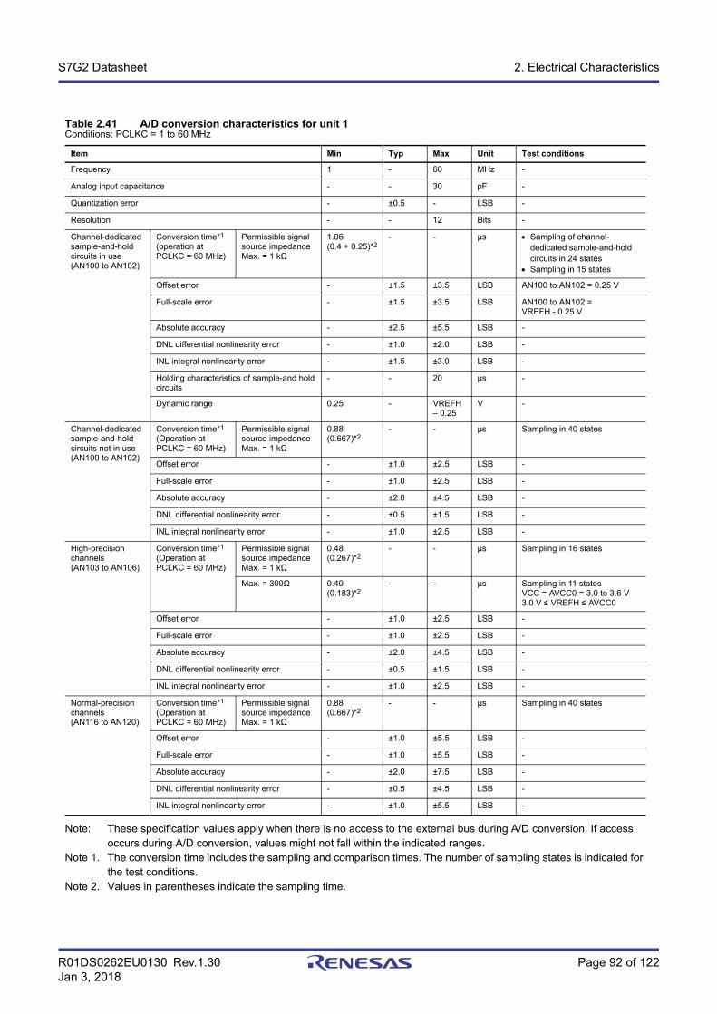
R01DS0262EU0130 Rev.1.30 Page 92 of 122Jan 3, 2018
S7G2 Datasheet 2. Electrical Characteristics
Note: These specification values apply when there is no access to the external bus during A/D conversion. If access occurs during A/D conversion, values might not fall within the indicated ranges.
Note 1. The conversion time includes the sampling and comparison times. The number of sampling states is indicated for the test conditions.
Note 2. Values in parentheses indicate the sampling time.
Table 2.41 A/D conversion characteristics for unit 1Conditions: PCLKC = 1 to 60 MHz
Item Min Typ Max Unit Test conditions
Frequency 1 - 60 MHz -
Analog input capacitance - - 30 pF -
Quantization error - ±0.5 - LSB -
Resolution - - 12 Bits -
Channel-dedicated sample-and-hold circuits in use (AN100 to AN102)
Conversion time*1 (operation at PCLKC = 60 MHz)
Permissible signal source impedance Max. = 1 kΩ
1.06 (0.4 + 0.25)*2
- - μs Sampling of channel-dedicated sample-and-hold circuits in 24 states
Sampling in 15 states
Offset error - ±1.5 ±3.5 LSB AN100 to AN102 = 0.25 V
Full-scale error - ±1.5 ±3.5 LSB AN100 to AN102 = VREFH - 0.25 V
Absolute accuracy - ±2.5 ±5.5 LSB -
DNL differential nonlinearity error - ±1.0 ±2.0 LSB -
INL integral nonlinearity error - ±1.5 ±3.0 LSB -
Holding characteristics of sample-and hold circuits
- - 20 μs -
Dynamic range 0.25 - VREFH – 0.25
V -
Channel-dedicated sample-and-hold circuits not in use (AN100 to AN102)
Conversion time*1 (Operation at PCLKC = 60 MHz)
Permissible signal source impedance Max. = 1 kΩ
0.88 (0.667)*2
- - μs Sampling in 40 states
Offset error - ±1.0 ±2.5 LSB -
Full-scale error - ±1.0 ±2.5 LSB -
Absolute accuracy - ±2.0 ±4.5 LSB -
DNL differential nonlinearity error - ±0.5 ±1.5 LSB -
INL integral nonlinearity error - ±1.0 ±2.5 LSB -
High-precision channels(AN103 to AN106)
Conversion time*1
(Operation at PCLKC = 60 MHz)
Permissible signal source impedance Max. = 1 kΩ
0.48 (0.267)*2
- - μs Sampling in 16 states
Max. = 300Ω 0.40 (0.183)*2
- - μs Sampling in 11 statesVCC = AVCC0 = 3.0 to 3.6 V3.0 V ≤ VREFH ≤ AVCC0
Offset error - ±1.0 ±2.5 LSB -
Full-scale error - ±1.0 ±2.5 LSB -
Absolute accuracy - ±2.0 ±4.5 LSB -
DNL differential nonlinearity error - ±0.5 ±1.5 LSB -
INL integral nonlinearity error - ±1.0 ±2.5 LSB -
Normal-precision channels(AN116 to AN120)
Conversion time*1 (Operation at PCLKC = 60 MHz)
Permissible signal source impedanceMax. = 1 kΩ
0.88 (0.667)*2
- - μs Sampling in 40 states
Offset error - ±1.0 ±5.5 LSB -
Full-scale error - ±1.0 ±5.5 LSB -
Absolute accuracy - ±2.0 ±7.5 LSB -
DNL differential nonlinearity error - ±0.5 ±4.5 LSB -
INL integral nonlinearity error - ±1.0 ±5.5 LSB -
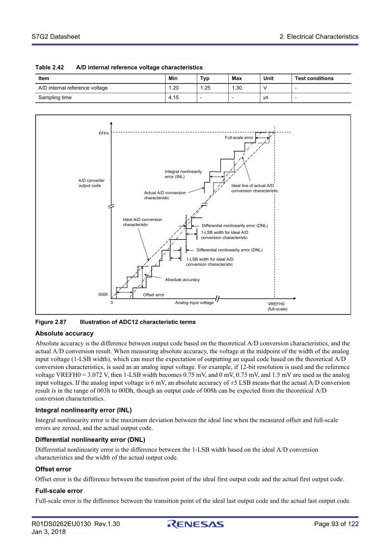
R01DS0262EU0130 Rev.1.30 Page 93 of 122Jan 3, 2018
S7G2 Datasheet 2. Electrical Characteristics
Figure 2.87 Illustration of ADC12 characteristic terms
Absolute accuracy
Absolute accuracy is the difference between output code based on the theoretical A/D conversion characteristics, and the actual A/D conversion result. When measuring absolute accuracy, the voltage at the midpoint of the width of the analog input voltage (1-LSB width), which can meet the expectation of outputting an equal code based on the theoretical A/D conversion characteristics, is used as an analog input voltage. For example, if 12-bit resolution is used and the reference voltage VREFH0 = 3.072 V, then 1-LSB width becomes 0.75 mV, and 0 mV, 0.75 mV, and 1.5 mV are used as the analog input voltages. If the analog input voltage is 6 mV, an absolute accuracy of ±5 LSB means that the actual A/D conversion result is in the range of 003h to 00Dh, though an output code of 008h can be expected from the theoretical A/D conversion characteristics.
Integral nonlinearity error (INL)
Integral nonlinearity error is the maximum deviation between the ideal line when the measured offset and full-scale errors are zeroed, and the actual output code.
Differential nonlinearity error (DNL)
Differential nonlinearity error is the difference between the 1-LSB width based on the ideal A/D conversion characteristics and the width of the actual output code.
Offset error
Offset error is the difference between the transition point of the ideal first output code and the actual first output code.
Full-scale error
Full-scale error is the difference between the transition point of the ideal last output code and the actual last output code.
Table 2.42 A/D internal reference voltage characteristics
Item Min Typ Max Unit Test conditions
A/D internal reference voltage 1.20 1.25 1.30 V -
Sampling time 4.15 - - μs -
Integral nonlinearity error (INL)
Actual A/D conversion characteristic
Ideal A/D conversion characteristic
Analog input voltage
Offset error
Absolute accuracy
Differential nonlinearity error (DNL)
Full-scale errorFFFh
000h
0
Ideal line of actual A/D conversion characteristic
1-LSB width for ideal A/D conversion characteristic
Differential nonlinearity error (DNL)
1-LSB width for ideal A/D conversion characteristic
VREFH0(full-scale)
A/D converteroutput code
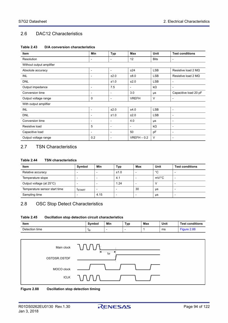
R01DS0262EU0130 Rev.1.30 Page 94 of 122Jan 3, 2018
S7G2 Datasheet 2. Electrical Characteristics
2.6 DAC12 Characteristics
2.7 TSN Characteristics
2.8 OSC Stop Detect Characteristics
Figure 2.88 Oscillation stop detection timing
Table 2.43 D/A conversion characteristics
Item Min Typ Max Unit Test conditions
Resolution - - 12 Bits -
Without output amplifier
Absolute accuracy - - ±24 LSB Resistive load 2 MΩ
INL - ±2.0 ±8.0 LSB Resistive load 2 MΩ
DNL ±1.0 ±2.0 LSB -
Output impedance - 7.5 - kΩ -
Conversion time - - 3.0 μs Capacitive load 20 pF
Output voltage range 0 - VREFH V -
With output amplifier
INL - ±2.0 ±4.0 LSB -
DNL - ±1.0 ±2.0 LSB -
Conversion time - - 4.0 μs -
Resistive load 5 - - kΩ -
Capacitive load - - 50 pF -
Output voltage range 0.2 - VREFH – 0.2 V -
Table 2.44 TSN characteristics
Item Symbol Min Typ Max Unit Test conditions
Relative accuracy - - ±1.0 - °C -
Temperature slope - - 4.1 - mV/°C -
Output voltage (at 25°C) - - 1.24 - V -
Temperature sensor start time tSTART - - 30 μs -
Sampling time - 4.15 - - μs -
Table 2.45 Oscillation stop detection circuit characteristics
Item Symbol Min Typ Max Unit Test conditions
Detection time tdr - - 1 ms Figure 2.88
tdr
Main clock
OSTDSR.OSTDF
MOCO clock
ICLK
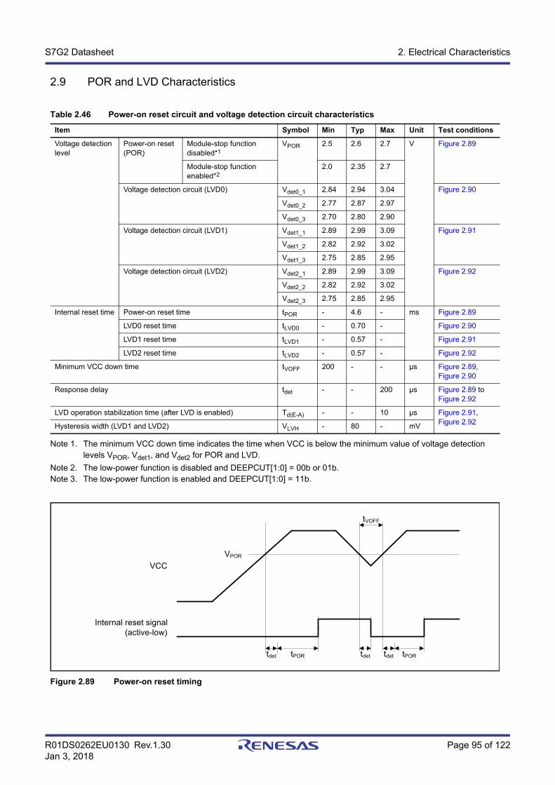
R01DS0262EU0130 Rev.1.30 Page 95 of 122Jan 3, 2018
S7G2 Datasheet 2. Electrical Characteristics
2.9 POR and LVD Characteristics
Note 1. The minimum VCC down time indicates the time when VCC is below the minimum value of voltage detection levels VPOR, Vdet1, and Vdet2 for POR and LVD.
Note 2. The low-power function is disabled and DEEPCUT[1:0] = 00b or 01b.Note 3. The low-power function is enabled and DEEPCUT[1:0] = 11b.
Figure 2.89 Power-on reset timing
Table 2.46 Power-on reset circuit and voltage detection circuit characteristics
Item Symbol Min Typ Max Unit Test conditions
Voltage detection level
Power-on reset (POR)
Module-stop function disabled*1
VPOR 2.5 2.6 2.7 V Figure 2.89
Module-stop function enabled*2
2.0 2.35 2.7
Voltage detection circuit (LVD0) Vdet0_1 2.84 2.94 3.04 Figure 2.90
Vdet0_2 2.77 2.87 2.97
Vdet0_3 2.70 2.80 2.90
Voltage detection circuit (LVD1) Vdet1_1 2.89 2.99 3.09 Figure 2.91
Vdet1_2 2.82 2.92 3.02
Vdet1_3 2.75 2.85 2.95
Voltage detection circuit (LVD2) Vdet2_1 2.89 2.99 3.09 Figure 2.92
Vdet2_2 2.82 2.92 3.02
Vdet2_3 2.75 2.85 2.95
Internal reset time Power-on reset time tPOR - 4.6 - ms Figure 2.89
LVD0 reset time tLVD0 - 0.70 - Figure 2.90
LVD1 reset time tLVD1 - 0.57 - Figure 2.91
LVD2 reset time tLVD2 - 0.57 - Figure 2.92
Minimum VCC down time tVOFF 200 - - μs Figure 2.89, Figure 2.90
Response delay tdet - - 200 μs Figure 2.89 to Figure 2.92
LVD operation stabilization time (after LVD is enabled) Td(E-A) - - 10 μs Figure 2.91, Figure 2.92
Hysteresis width (LVD1 and LVD2) VLVH - 80 - mV
Internal reset signal(active-low)
VCC
tVOFF
tdet tPORtdettPORtdet
VPOR
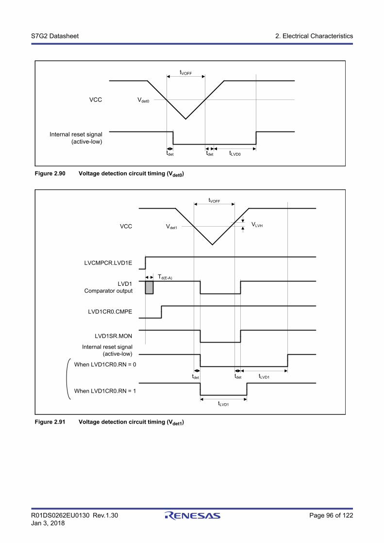
R01DS0262EU0130 Rev.1.30 Page 96 of 122Jan 3, 2018
S7G2 Datasheet 2. Electrical Characteristics
Figure 2.90 Voltage detection circuit timing (Vdet0)
Figure 2.91 Voltage detection circuit timing (Vdet1)
tVOFF
tLVD0tdet
Vdet0VCC
Internal reset signal(active-low)
tdet
tVOFF
Vdet1VCC
tdettdet
tLVD1
Td(E-A)
LVCMPCR.LVD1E
LVD1Comparator output
LVD1CR0.CMPE
LVD1SR.MON
Internal reset signal(active-low)
When LVD1CR0.RN = 0
When LVD1CR0.RN = 1
VLVH
tLVD1
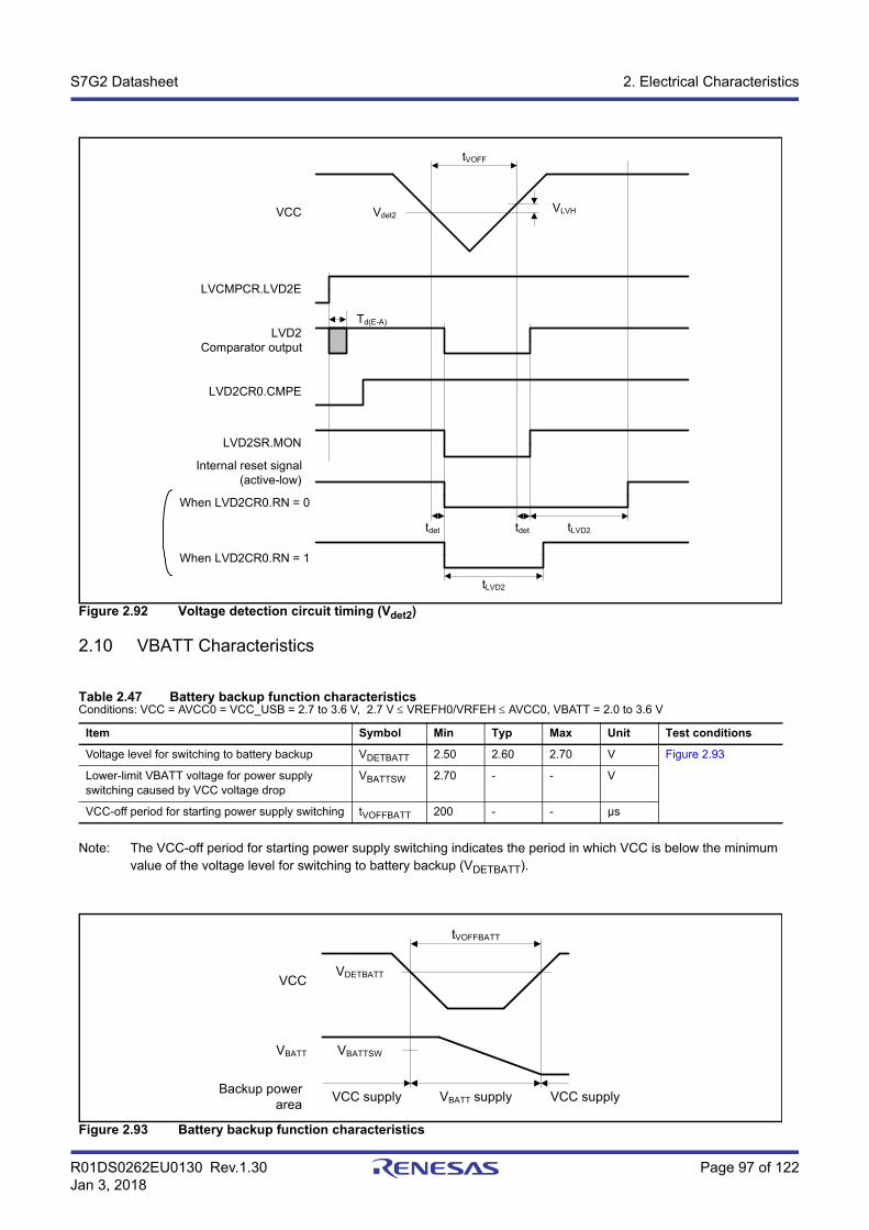
R01DS0262EU0130 Rev.1.30 Page 97 of 122Jan 3, 2018
S7G2 Datasheet 2. Electrical Characteristics
Figure 2.92 Voltage detection circuit timing (Vdet2)
2.10 VBATT Characteristics
Note: The VCC-off period for starting power supply switching indicates the period in which VCC is below the minimum value of the voltage level for switching to battery backup (VDETBATT).
Figure 2.93 Battery backup function characteristics
Table 2.47 Battery backup function characteristicsConditions: VCC = AVCC0 = VCC_USB = 2.7 to 3.6 V, 2.7 V VREFH0/VRFEH AVCC0, VBATT = 2.0 to 3.6 V
Item Symbol Min Typ Max Unit Test conditions
Voltage level for switching to battery backup VDETBATT 2.50 2.60 2.70 V Figure 2.93
Lower-limit VBATT voltage for power supply switching caused by VCC voltage drop
VBATTSW 2.70 - - V
VCC-off period for starting power supply switching tVOFFBATT 200 - - μs
tVOFF
Vdet2VCC
tdettdet
tLVD2
Td(E-A)
VLVH
tLVD2
LVCMPCR.LVD2E
LVD2Comparator output
LVD2CR0.CMPE
LVD2SR.MON
Internal reset signal(active-low)
When LVD2CR0.RN = 0
When LVD2CR0.RN = 1
VCC
tVOFFBATT
VDETBATT
VBATTSWVBATT
VCC supplyVBATT supplyVCC supplyBackup power
area
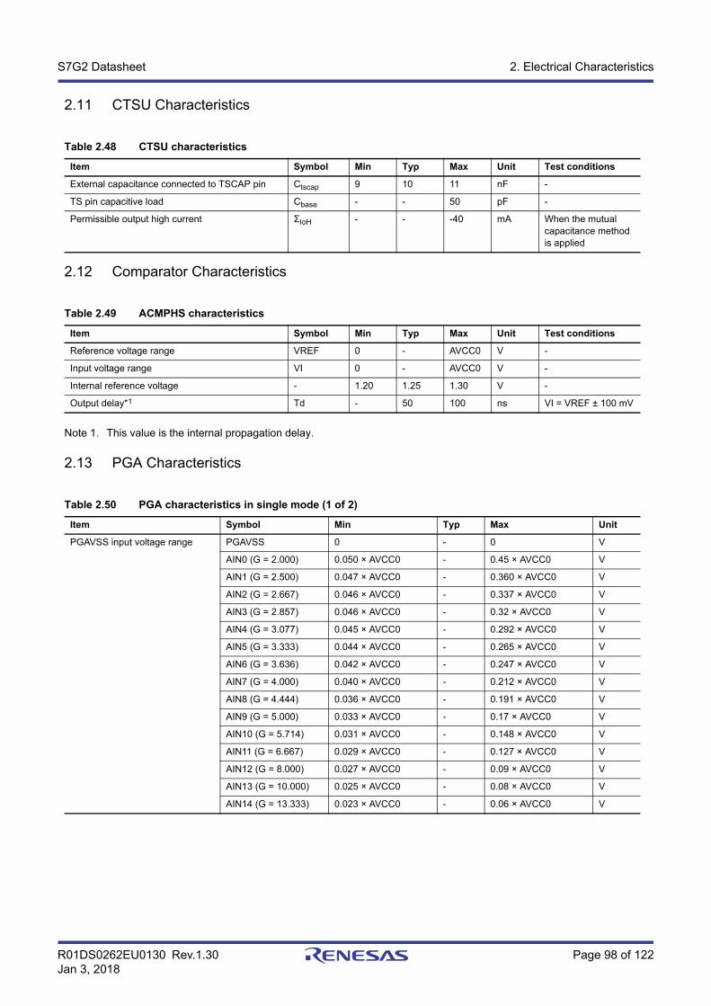
R01DS0262EU0130 Rev.1.30 Page 98 of 122Jan 3, 2018
S7G2 Datasheet 2. Electrical Characteristics
2.11 CTSU Characteristics
2.12 Comparator Characteristics
Note 1. This value is the internal propagation delay.
2.13 PGA Characteristics
Table 2.48 CTSU characteristics
Item Symbol Min Typ Max Unit Test conditions
External capacitance connected to TSCAP pin Ctscap 9 10 11 nF -
TS pin capacitive load Cbase - - 50 pF -
Permissible output high current ΣIoH - - -40 mA When the mutual capacitance method is applied
Table 2.49 ACMPHS characteristics
Item Symbol Min Typ Max Unit Test conditions
Reference voltage range VREF 0 - AVCC0 V -
Input voltage range VI 0 - AVCC0 V -
Internal reference voltage - 1.20 1.25 1.30 V -
Output delay*1 Td - 50 100 ns VI = VREF ± 100 mV
Table 2.50 PGA characteristics in single mode (1 of 2)
Item Symbol Min Typ Max Unit
PGAVSS input voltage range PGAVSS 0 - 0 V
AIN0 (G = 2.000) 0.050 × AVCC0 - 0.45 × AVCC0 V
AIN1 (G = 2.500) 0.047 × AVCC0 - 0.360 × AVCC0 V
AIN2 (G = 2.667) 0.046 × AVCC0 - 0.337 × AVCC0 V
AIN3 (G = 2.857) 0.046 × AVCC0 - 0.32 × AVCC0 V
AIN4 (G = 3.077) 0.045 × AVCC0 - 0.292 × AVCC0 V
AIN5 (G = 3.333) 0.044 × AVCC0 - 0.265 × AVCC0 V
AIN6 (G = 3.636) 0.042 × AVCC0 - 0.247 × AVCC0 V
AIN7 (G = 4.000) 0.040 × AVCC0 - 0.212 × AVCC0 V
AIN8 (G = 4.444) 0.036 × AVCC0 - 0.191 × AVCC0 V
AIN9 (G = 5.000) 0.033 × AVCC0 - 0.17 × AVCC0 V
AIN10 (G = 5.714) 0.031 × AVCC0 - 0.148 × AVCC0 V
AIN11 (G = 6.667) 0.029 × AVCC0 - 0.127 × AVCC0 V
AIN12 (G = 8.000) 0.027 × AVCC0 - 0.09 × AVCC0 V
AIN13 (G = 10.000) 0.025 × AVCC0 - 0.08 × AVCC0 V
AIN14 (G = 13.333) 0.023 × AVCC0 - 0.06 × AVCC0 V
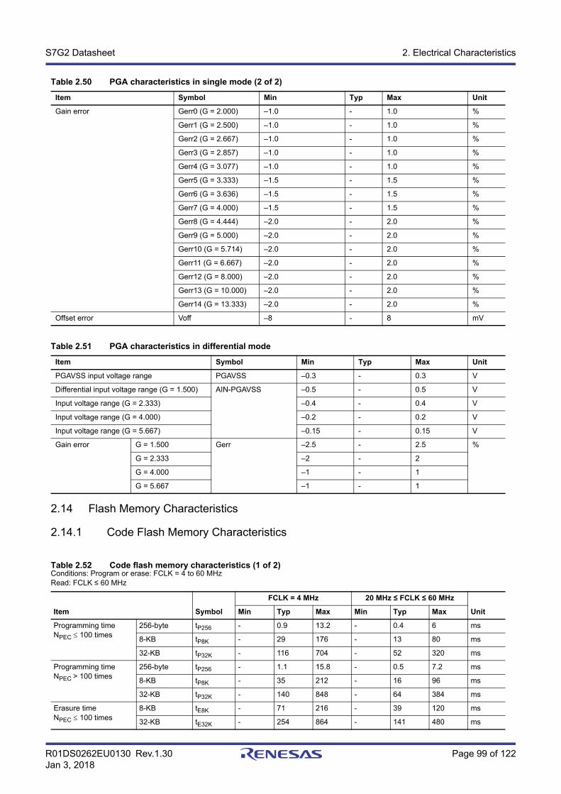
R01DS0262EU0130 Rev.1.30 Page 99 of 122Jan 3, 2018
S7G2 Datasheet 2. Electrical Characteristics
2.14 Flash Memory Characteristics
2.14.1 Code Flash Memory Characteristics
Gain error Gerr0 (G = 2.000) –1.0 - 1.0 %
Gerr1 (G = 2.500) –1.0 - 1.0 %
Gerr2 (G = 2.667) –1.0 - 1.0 %
Gerr3 (G = 2.857) –1.0 - 1.0 %
Gerr4 (G = 3.077) –1.0 - 1.0 %
Gerr5 (G = 3.333) –1.5 - 1.5 %
Gerr6 (G = 3.636) –1.5 - 1.5 %
Gerr7 (G = 4.000) –1.5 - 1.5 %
Gerr8 (G = 4.444) –2.0 - 2.0 %
Gerr9 (G = 5.000) –2.0 - 2.0 %
Gerr10 (G = 5.714) –2.0 - 2.0 %
Gerr11 (G = 6.667) –2.0 - 2.0 %
Gerr12 (G = 8.000) –2.0 - 2.0 %
Gerr13 (G = 10.000) –2.0 - 2.0 %
Gerr14 (G = 13.333) –2.0 - 2.0 %
Offset error Voff –8 - 8 mV
Table 2.51 PGA characteristics in differential mode
Item Symbol Min Typ Max Unit
PGAVSS input voltage range PGAVSS –0.3 - 0.3 V
Differential input voltage range (G = 1.500) AIN-PGAVSS –0.5 - 0.5 V
Input voltage range (G = 2.333) –0.4 - 0.4 V
Input voltage range (G = 4.000) –0.2 - 0.2 V
Input voltage range (G = 5.667) –0.15 - 0.15 V
Gain error G = 1.500 Gerr –2.5 - 2.5 %
G = 2.333 –2 - 2
G = 4.000 –1 - 1
G = 5.667 –1 - 1
Table 2.52 Code flash memory characteristics (1 of 2)Conditions: Program or erase: FCLK = 4 to 60 MHzRead: FCLK ≤ 60 MHz
Item Symbol
FCLK = 4 MHz 20 MHz ≤ FCLK ≤ 60 MHz
UnitMin Typ Max Min Typ Max
Programming timeNPEC 100 times
256-byte tP256 - 0.9 13.2 - 0.4 6 ms
8-KB tP8K - 29 176 - 13 80 ms
32-KB tP32K - 116 704 - 52 320 ms
Programming timeNPEC > 100 times
256-byte tP256 - 1.1 15.8 - 0.5 7.2 ms
8-KB tP8K - 35 212 - 16 96 ms
32-KB tP32K - 140 848 - 64 384 ms
Erasure timeNPEC 100 times
8-KB tE8K - 71 216 - 39 120 ms
32-KB tE32K - 254 864 - 141 480 ms
Table 2.50 PGA characteristics in single mode (2 of 2)
Item Symbol Min Typ Max Unit
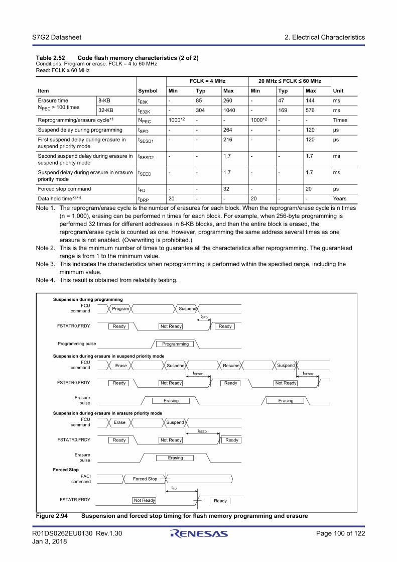
R01DS0262EU0130 Rev.1.30 Page 100 of 122Jan 3, 2018
S7G2 Datasheet 2. Electrical Characteristics
Note 1. The reprogram/erase cycle is the number of erasures for each block. When the reprogram/erase cycle is n times (n = 1,000), erasing can be performed n times for each block. For example, when 256-byte programming is performed 32 times for different addresses in 8-KB blocks, and then the entire block is erased, the reprogram/erase cycle is counted as one. However, programming the same address several times as one erasure is not enabled. (Overwriting is prohibited.)
Note 2. This is the minimum number of times to guarantee all the characteristics after reprogramming. The guaranteed range is from 1 to the minimum value.
Note 3. This indicates the characteristics when reprogramming is performed within the specified range, including the minimum value.
Note 4. This result is obtained from reliability testing.
Figure 2.94 Suspension and forced stop timing for flash memory programming and erasure
Erasure timeNPEC > 100 times
8-KB tE8K - 85 260 - 47 144 ms
32-KB tE32K - 304 1040 - 169 576 ms
Reprogramming/erasure cycle*1 NPEC 1000*2 - - 1000*2 - - Times
Suspend delay during programming tSPD - - 264 - - 120 μs
First suspend delay during erasure in suspend priority mode
tSESD1 - - 216 - - 120 μs
Second suspend delay during erasure in suspend priority mode
tSESD2 - - 1.7 - - 1.7 ms
Suspend delay during erasure in erasure priority mode
tSEED - - 1.7 - - 1.7 ms
Forced stop command tFD - - 32 - - 20 μs
Data hold time*3*4 tDRP 20 - - 20 - - Years
Table 2.52 Code flash memory characteristics (2 of 2)Conditions: Program or erase: FCLK = 4 to 60 MHzRead: FCLK ≤ 60 MHz
Item Symbol
FCLK = 4 MHz 20 MHz ≤ FCLK ≤ 60 MHz
UnitMin Typ Max Min Typ Max
FCU command
FSTATR0.FRDY
Programming pulse
Suspension during programming
FCU command
FSTATR0.FRDY
Erasure pulse
Suspension during erasure in suspend priority mode
FCU command
FSTATR0.FRDY
Erasure pulse
Suspension during erasure in erasure priority mode
Program Suspend
Ready Not Ready Ready
Programming
tSPD
Erase Suspend
Ready Not Ready Ready
tSEED
Erasing
Erase Suspend Resume Suspend
Ready Not Ready Ready Not Ready
tSESD1 tSESD2
Erasing Erasing
tFD
Forced Stop
FACI command
FSTATR.FRDY
Forced Stop
Not Ready Ready
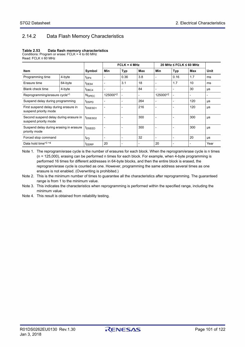
R01DS0262EU0130 Rev.1.30 Page 101 of 122Jan 3, 2018
S7G2 Datasheet 2. Electrical Characteristics
2.14.2 Data Flash Memory Characteristics
Note 1. The reprogram/erase cycle is the number of erasures for each block. When the reprogram/erase cycle is n times (n = 125,000), erasing can be performed n times for each block. For example, when 4-byte programming is performed 16 times for different addresses in 64-byte blocks, and then the entire block is erased, the reprogram/erase cycle is counted as one. However, programming the same address several times as one erasure is not enabled. (Overwriting is prohibited.)
Note 2. This is the minimum number of times to guarantee all the characteristics after reprogramming. The guaranteed range is from 1 to the minimum value.
Note 3. This indicates the characteristics when reprogramming is performed within the specified range, including the minimum value.
Note 4. This result is obtained from reliability testing.
Table 2.53 Data flash memory characteristicsConditions: Program or erase: FCLK = 4 to 60 MHzRead: FCLK ≤ 60 MHz
Item Symbol
FCLK = 4 MHz 20 MHz ≤ FCLK ≤ 60 MHz
UnitMin Typ Max Min Typ Max
Programming time 4-byte tDP4 - 0.36 3.8 - 0.16 1.7 ms
Erasure time 64-byte tDE64 - 3.1 18 - 1.7 10 ms
Blank check time 4-byte tDBC4 - - 84 - - 30 μs
Reprogramming/erasure cycle*1 NDPEC 125000*2 - - 125000*2 - - -
Suspend delay during programming tDSPD - - 264 - - 120 μs
First suspend delay during erasure in suspend priority mode
tDSESD1 - - 216 - - 120 μs
Second suspend delay during erasure in suspend priority mode
tDSESD2 - - 300 - - 300 μs
Suspend delay during erasing in erasure priority mode
tDSEED - - 300 - - 300 μs
Forced stop command tFD - - 32 - - 20 μs
Data hold time*3 *4 tDDRP 20 - - 20 - - Year
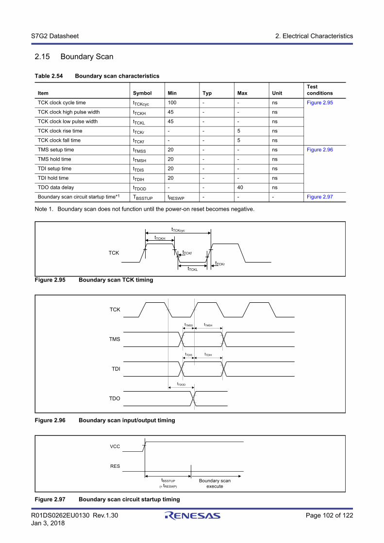
R01DS0262EU0130 Rev.1.30 Page 102 of 122Jan 3, 2018
S7G2 Datasheet 2. Electrical Characteristics
2.15 Boundary Scan
Note 1. Boundary scan does not function until the power-on reset becomes negative.
Figure 2.95 Boundary scan TCK timing
Figure 2.96 Boundary scan input/output timing
Figure 2.97 Boundary scan circuit startup timing
Table 2.54 Boundary scan characteristics
Item Symbol Min Typ Max UnitTest conditions
TCK clock cycle time tTCKcyc 100 - - ns Figure 2.95
TCK clock high pulse width tTCKH 45 - - ns
TCK clock low pulse width tTCKL 45 - - ns
TCK clock rise time tTCKr - - 5 ns
TCK clock fall time tTCKf - - 5 ns
TMS setup time tTMSS 20 - - ns Figure 2.96
TMS hold time tTMSH 20 - - ns
TDI setup time tTDIS 20 - - ns
TDI hold time tTDIH 20 - - ns
TDO data delay tTDOD - - 40 ns
Boundary scan circuit startup time*1 TBSSTUP tRESWP - - - Figure 2.97
tTCKcyc
tTCKH
tTCKf
tTCKL
tTCKr
TCK
tTMSS tTMSH
tTDIS tTDIH
tTDOD
TCK
TMS
TDI
TDO
VCC
RES
Boundary scan execute
tBSSTUP
(= tRESWP)
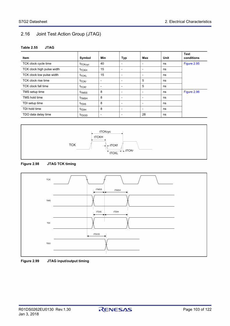
R01DS0262EU0130 Rev.1.30 Page 103 of 122Jan 3, 2018
S7G2 Datasheet 2. Electrical Characteristics
2.16 Joint Test Action Group (JTAG)
Figure 2.98 JTAG TCK timing
Figure 2.99 JTAG input/output timing
Table 2.55 JTAG
Item Symbol Min Typ Max UnitTest conditions
TCK clock cycle time tTCKcyc 40 - - ns Figure 2.95
TCK clock high pulse width tTCKH 15 - - ns
TCK clock low pulse width tTCKL 15 - - ns
TCK clock rise time tTCKr - - 5 ns
TCK clock fall time tTCKf - - 5 ns
TMS setup time tTMSS 8 - - ns Figure 2.96
TMS hold time tTMSH 8 - - ns
TDI setup time tTDIS 8 - - ns
TDI hold time tTDIH 8 - - ns
TDO data delay time tTDOD - - 28 ns
TCK
tTCKH
tTCKcyc
tTCKL
tTCKf
tTCKr
TCK
TMS
tTMSS tTMSH
TDI
tTDIS tTDIH
TDO
tTDOD
R01DS0262EU0130 Rev.1.30 Page 104 of 122Jan 3, 2018
S7G2 Datasheet 2. Electrical Characteristics
2.17 Serial Wire Debug (SWD)
Figure 2.100 SWD SWCLK timing
Figure 2.101 SWD input/output timing
Table 2.56 SWD
Item Symbol Min Typ Max UnitTest conditions
SWCLK clock cycle time tSWCKcyc 40 - - ns Figure 2.100
SWCLK clock high pulse width tSWCKH 15 - - ns
SWCLK clock low pulse width tSWCKL 15 - - ns
SWCLK clock rise time tSWCKr - - 5 ns
SWCLK clock fall time tSWCKf - - 5 ns
SWDIO setup time tSWDS 8 - - ns Figure 2.101
SWDIO hold time tSWDH 8 - - ns
SWDIO data delay time tSWDD 2 - 28 ns
SWCLK
tSWCKH
tSWCKcyc
tSWCKL
SWCLK
SWDIO(Input)
tSWDS tSWDH
SWDIO(Output)
tSWDD
SWDIO(Output)
tSWDD
SWDIO(Output)
tSWDD
R01DS0262EU0130 Rev.1.30 Page 105 of 122Jan 3, 2018
S7G2 Datasheet 2. Electrical Characteristics
2.18 Embedded Trace Macro Interface (ETM)
Figure 2.102 ETM TCLK timing
Figure 2.103 ETM output timing
Table 2.57 ETM
Item Symbol Min Typ Max UnitTest conditions
TCLK clock cycle time tTCLKcyc 16.6 - - ns Figure 2.102
TCLK clock high pulse width tTCLKH 5.8 - - ns
TCLK clock low pulse width tTCLKL 5.8 - - ns
TCLK clock rise time tTCLKr - - 2.5 ns
TCLK clock fall time tTCLKf - - 2.5 ns
TDATA0-3 output setup time tTRDS 1.6 - - ns Figure 2.103
TDATA0-3 output hold time tTRDH 1.6 - - ns
TCLK
tTCLKH
tTCLKcyc
tTCLKL
tTCLKf
tTCLKr
TDATA0-3
TCLK
tTRDS tTRDStTRDH tTRDH
R01DS0262EU0130 Rev.1.30 Page 106 of 122Jan 3, 2018
S7G2 Datasheet Appendix 1. Package Dimensions
Appendix 1. Package DimensionsFor information on the latest version of the package dimensions or mountings, go to “Packages” on the Renesas Electronics Corporation website.
Figure 1.1 224-pin BGA
MASS (Typ) [g]
0.4
Unit: mm
Previous CodeRENESAS Code
PLBG0224GA-A 224FHE
JEITA Package Code
DEAA1
ebx1
x2
yy1
nZD
ZE
12.912.9
0.30
0.40
P-LFBGA224-13x13-0.80
Min NomDimensions in millimetersReference
Symbol
13.013.0
0.350.800.45
2240.900.90
13.113.11.400.40
0.500.150.080.100.20
Max
© 2016 Renesas Electronics Corporation. All rights reserved.
y CZ
S
y1 S
A
A1
(ZE)
e
e
(ZD)
INDEX AREA
B EA
D
ABCDEFGH
JKLMNPR
1 2 3 4 5 6 7 8 9 10 11 12 13 14 15
n x b x1 S A Bx2 S
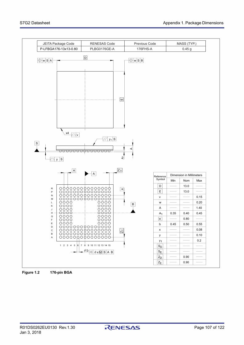
R01DS0262EU0130 Rev.1.30 Page 107 of 122Jan 3, 2018
S7G2 Datasheet Appendix 1. Package Dimensions
Figure 1.2 176-pin BGA
JEITA Package Code RENESAS Code Previous Code MASS (TYP.) PLBG0176GE-A 176FHS-A 0.45 gP-LFBGA176-13x13-0.80
e
A1
MaxNomMin
Dimension in MillimetersSymbol
Reference
A
b
x
y
13.0
0.10
0.80
0.45 0.50 0.55
0.35 0.40 0.45
1.40
13.0
0.08
v
w
0.90
0.90
y1 0.2
0.20
0.15
ZE
ZD
SE
SD
E
D
1E
D
1
A
x4
A
B
x M S A B
S
Sy
Sw A Sw B
vSy1
2 3 4 5 6 7 8 9 10 11 12 13 14 15
BCDEFGHJKLMNPR
Ze
e Z
A
AE
D
b
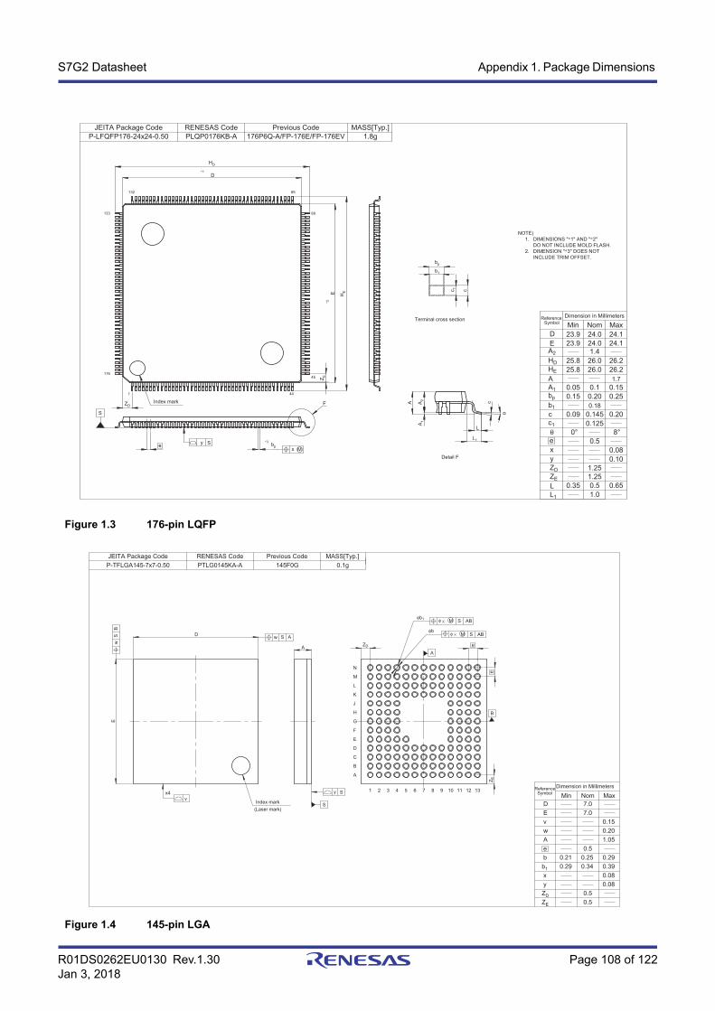
R01DS0262EU0130 Rev.1.30 Page 108 of 122Jan 3, 2018
S7G2 Datasheet Appendix 1. Package Dimensions
Figure 1.3 176-pin LQFP
Figure 1.4 145-pin LGA
NOTE)
1. DIMENSIONS "*1" AND "*2"
DO NOT INCLUDE MOLD FLASH.
2. DIMENSION "*3" DOES NOT
INCLUDE TRIM OFFSET.
Dimension in MillimetersReferenceSymbol Min Nom Max
bp
b1
c1
c
*2
E HE
*1
D
HD
Terminal cross section
Detail F
θ
c
L
F
M
S
S
ye
L1
A1
A2
A
xbp
*3
Index markZD
ZE
1
176
133
132 89
88
45
44
23.9 24.0 24.1
23.9 24.01.4
24.1
25.8 26.0 26.2
25.8 26.0 26.2
0.05 0.1
0.18
0.15
0.15 0.20 0.25
0.09 0.145
0.125
0.5
1.0
1.25
1.25
0° 8°
0.20
0.35 0.5 0.65
0.08
0.10
1.7
JEITA Package Code RENESAS Code Previous Code MASS[Typ.]
P-LFQFP176-24x24-0.50 PLQP0176KB-A 176P6Q-A/FP-176E/FP-176EV 1.8g
L1
c1
θ
b1
A1
A2
A
bp
HE
E
D
HD
ZE
ZD
L
y
x
e
c
0.5ZE
ZD 0.5
0.290.250.21b
b1
y 0.08
e 0.5
x
A 1.05
E 7.0
D 7.0
ReferenceSymbol
Dimension in Millimeters
Min Nom Max
0.29 0.34 0.39
0.08
w 0.20
v 0.15
PTLG0145KA-A 145F0GP-TFLGA145-7x7-0.50 0.1g
MASS[Typ.]RENESAS CodeJEITA Package Code Previous Code
131211109
N
M
L
K
J
Index mark
(Laser mark)
x4
v
AB
A
B
S
AB
S
S
y
S
87654321
B
C
D
E
F
G
H
A
S Aw S
wB
ZE
ZDA
e
e
E
D
φb1M
φb
φ
φ M
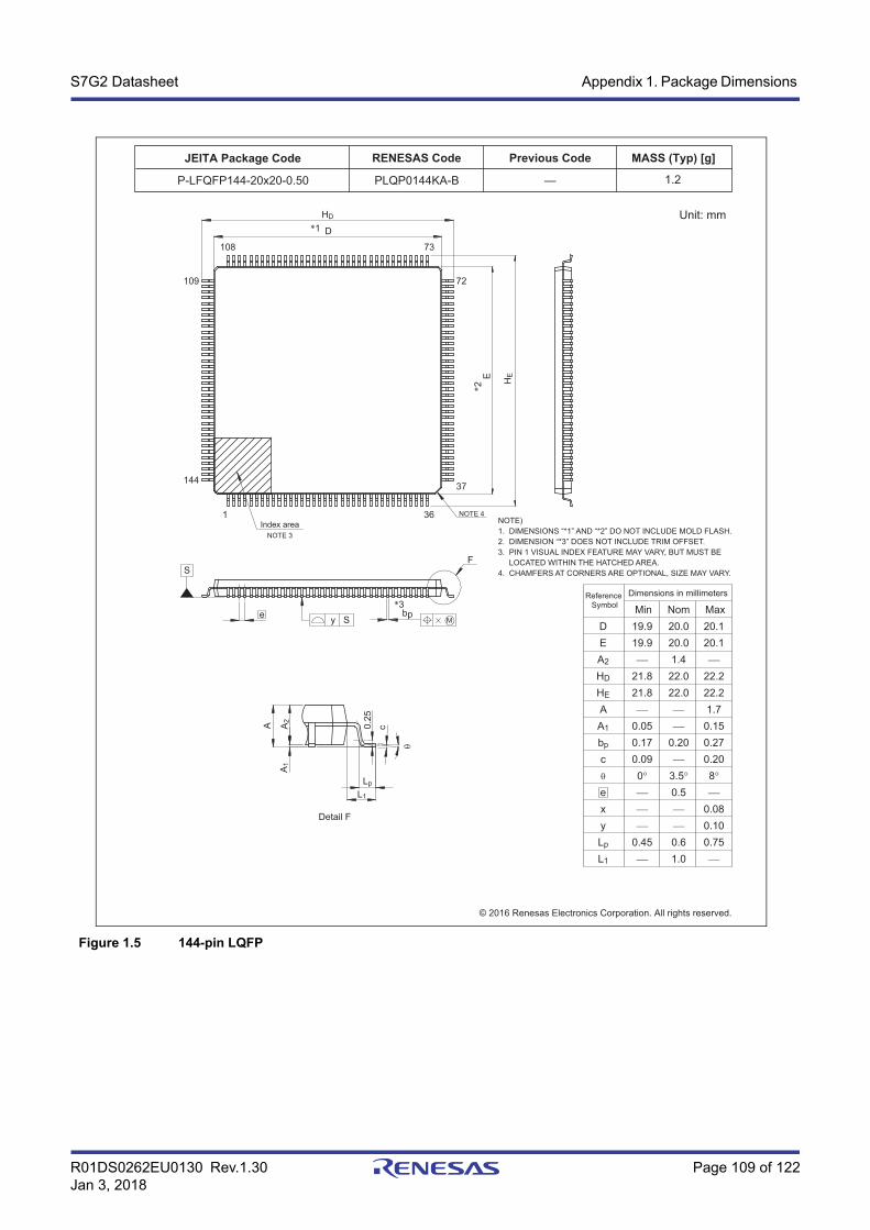
R01DS0262EU0130 Rev.1.30 Page 109 of 122Jan 3, 2018
S7G2 Datasheet Appendix 1. Package Dimensions
Figure 1.5 144-pin LQFP
MASS (Typ) [g]
1.2
Unit: mm
Previous CodeRENESAS Code
PLQP0144KA-B —
JEITA Package Code
P-LFQFP144-20x20-0.50
© 2016 Renesas Electronics Corporation. All rights reserved.
DEA2
HD
HE
AA1
bp
c
exyLp
L1
19.919.9
21.821.8
0.050.170.090
0.45
Min NomDimensions in millimetersReference
Symbol Max20.020.01.422.022.0
0.20
3.50.5
0.61.0
20.120.1
22.222.21.7
0.150.270.208
0.080.100.75
NOTE)1. DIMENSIONS “*1” AND “*2” DO NOT INCLUDE MOLD FLASH.2. DIMENSION “*3” DOES NOT INCLUDE TRIM OFFSET.3. PIN 1 VISUAL INDEX FEATURE MAY VARY, BUT MUST BE LOCATED WITHIN THE HATCHED AREA.4. CHAMFERS AT CORNERS ARE OPTIONAL, SIZE MAY VARY.
HD
A2
A1
Lp
L1
Detail F
A c0.25
HE
D
E
108 73
72
37
109
144
1 36
F
NOTE 4
NOTE 3Index area
*1
*2
*3bpe y S
S
M
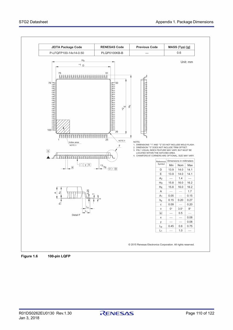
R01DS0262EU0130 Rev.1.30 Page 110 of 122Jan 3, 2018
S7G2 Datasheet Appendix 1. Package Dimensions
Figure 1.6 100-pin LQFP
MASS (Typ) [g]
0.6
Unit: mm
Previous CodeRENESAS Code
PLQP0100KB-B —
JEITA Package Code
P-LFQFP100-14x14-0.50
© 2015 Renesas Electronics Corporation. All rights reserved.
DEA2
HD
HE
AA1
bp
c
exyLp
L1
13.913.9
15.815.8
0.050.150.090
0.45
Min NomDimensions in millimetersReference
Symbol Max14.014.01.4
16.016.0
0.20
3.50.5
0.61.0
14.114.1
16.216.21.7
0.150.270.208
0.080.080.75
NOTE)1. DIMENSIONS “*1” AND “*2” DO NOT INCLUDE MOLD FLASH.2. DIMENSION “*3” DOES NOT INCLUDE TRIM OFFSET.3. PIN 1 VISUAL INDEX FEATURE MAY VARY, BUT MUST BE LOCATED WITHIN THE HATCHED AREA.4. CHAMFERS AT CORNERS ARE OPTIONAL, SIZE MAY VARY.
HDA
2A
1
Lp
L1
Detail F
A c0.25
D
75
76
10026
251
50
51
F
NOTE 4
NOTE 3Index area
*1
HEE
*2
*3 bpey S
S
M
S7G2 Microcontroller Group Datasheet
Proprietary NoticeAll text, graphics, photographs, trademarks, logos, artwork and computer code, collectively known as content, contained in this document is owned, controlled or licensed by or to Renesas, and is protected by trade dress, copyright, patent and trademark laws, and other intellectual property rights and unfair competition laws. Except as expressly provided herein, no part of this document or content may be copied, reproduced, republished, posted, publicly displayed, encoded, translated, transmitted or distributed in any other medium for publication or distribution or for any commercial enterprise, without prior written consent from Renesas.
Arm® and Cortex® are registered trademarks of Arm Limited. CoreSight™ is a trademark of Arm Limited.
CoreMark® is a registered trademark of the Embedded Microprocessor Benchmark Consortium.
Magic Packet™ is a trademark of Advanced Micro Devices, Inc.
SuperFlash® is a registered trademark of Silicon Storage Technology, Inc. in several countries including the United States and Japan.
Other brands and names mentioned in this document may be the trademarks or registered trademarks of their respectiveholders.
Rev. Date Summary
1.00 Feb 23, 2016 1st release
1.30 Jan 3, 2018 Updated for 1.30
Revision History

S7G2 Microcontroller Group Datasheet
Publication Date: Rev.1.30 Jan 3, 2018
Published by: Renesas Electronics Corporation
Colophon
Address ListGeneral Precautions
1. Precaution against Electrostatic Discharge (ESD) A strong electrical field, when exposed to a CMOS device, can cause destruction of the gate oxide and ultimately
degrade the device operation. Steps must be taken to stop the generation of static electricity as much as possible, and quickly dissipate it when it occurs. Environmental control must be adequate. When it is dry, a humidifier should be used. This is recommended to avoid using insulators that can easily build up static electricity. Semiconductor devices must be stored and transported in an anti-static container, static shielding bag or conductive material. All test and measurement tools including work benches and floors must be grounded. The operator must also be grounded using a wrist strap. Semiconductor devices must not be touched with bare hands. Similar precautions must be taken for printed circuit boards with mounted semiconductor devices.
2. Processing at power-on The state of the product is undefined at the time when power is supplied. The states of internal circuits in the LSI are
indeterminate and the states of register settings and pins are undefined at the time when power is supplied. In a finished product where the reset signal is applied to the external reset pin, the states of pins are not guaranteed from the time when power is supplied until the reset process is completed. In a similar way, the states of pins in a product that is reset by an on-chip power-on reset function are not guaranteed from the time when power is supplied until the power reaches the level at which resetting is specified.
3. Input of signal during power-off state Do not input signals or an I/O pull-up power supply while the device is powered off. The current injection that results
from input of such a signal or I/O pull-up power supply may cause malfunction and the abnormal current that passes in the device at this time may cause degradation of internal elements. Follow the guideline for input signal during power-off state as described in your product documentation.
4. Handling of unused pins Handle unused pins in accordance with the directions given under handling of unused pins in the manual. The input pins
of CMOS products are generally in the high-impedance state. In operation with an unused pin in the open-circuit state, extra electromagnetic noise is induced in the vicinity of the LSI, an associated shoot-through current flows internally, and malfunctions occur due to the false recognition of the pin state as an input signal become possible.
5. Clock signals After applying a reset, only release the reset line after the operating clock signal becomes stable. When switching the
clock signal during program execution, wait until the target clock signal is stabilized. When the clock signal is generated with an external resonator or from an external oscillator during a reset, ensure that the reset line is only released after full stabilization of the clock signal. Additionally, when switching to a clock signal produced with an external resonator or by an external oscillator while program execution is in progress, wait until the target clock signal is stable.
6. Voltage application waveform at input pin Waveform distortion due to input noise or a reflected wave may cause malfunction. If the input of the CMOS device
stays in the area between VIL (Max.) and VIH (Min.) due to noise, for example, the device may malfunction. Take care to prevent chattering noise from entering the device when the input level is fixed, and also in the transition period when the input level passes through the area between VIL (Max.) and VIH (Min.).
7. Prohibition of access to reserved addressesAccess to reserved addresses is prohibited. The reserved addresses are provided for possible future expansion of functions. Do not access these addresses as the correct operation of the LSI is not guaranteed.
8. Differences between products Before changing from one product to another, for example to a product with a different part number, confirm that the
change will not lead to problems. The characteristics of a microprocessing unit or microcontroller unit products in the same group but having a different part number might differ in terms of internal memory capacity, layout pattern, and other factors, which can affect the ranges of electrical characteristics, such as characteristic values, operating margins, immunity to noise, and amount of radiated noise. When changing to a product with a different part number, implement a system-evaluation test for the given product.
http://www.renesas.com Refer to "http://www.renesas.com/" for the latest and detailed information.
Renesas Electronics America Inc.1001 Murphy Ranch Road, Milpitas, CA 95035, U.S.A.Tel: +1-408-432-8888, Fax: +1-408-434-5351Renesas Electronics Canada Limited9251 Yonge Street, Suite 8309 Richmond Hill, Ontario Canada L4C 9T3Tel: +1-905-237-2004Renesas Electronics Europe LimitedDukes Meadow, Millboard Road, Bourne End, Buckinghamshire, SL8 5FH, U.KTel: +44-1628-651-700, Fax: +44-1628-651-804Renesas Electronics Europe GmbHArcadiastrasse 10, 40472 Düsseldorf, Germany Tel: +49-211-6503-0, Fax: +49-211-6503-1327Renesas Electronics (China) Co., Ltd.Room 1709 Quantum Plaza, No.27 ZhichunLu, Haidian District, Beijing, 100191 P. R. ChinaTel: +86-10-8235-1155, Fax: +86-10-8235-7679Renesas Electronics (Shanghai) Co., Ltd.Unit 301, Tower A, Central Towers, 555 Langao Road, Putuo District, Shanghai, 200333 P. R. China Tel: +86-21-2226-0888, Fax: +86-21-2226-0999Renesas Electronics Hong Kong LimitedUnit 1601-1611, 16/F., Tower 2, Grand Century Place, 193 Prince Edward Road West, Mongkok, Kowloon, Hong KongTel: +852-2265-6688, Fax: +852 2886-9022Renesas Electronics Taiwan Co., Ltd.13F, No. 363, Fu Shing North Road, Taipei 10543, TaiwanTel: +886-2-8175-9600, Fax: +886 2-8175-9670Renesas Electronics Singapore Pte. Ltd.80 Bendemeer Road, Unit #06-02 Hyflux Innovation Centre, Singapore 339949Tel: +65-6213-0200, Fax: +65-6213-0300Renesas Electronics Malaysia Sdn.Bhd.Unit 1207, Block B, Menara Amcorp, Amcorp Trade Centre, No. 18, Jln Persiaran Barat, 46050 Petaling Jaya, Selangor Darul Ehsan, MalaysiaTel: +60-3-7955-9390, Fax: +60-3-7955-9510Renesas Electronics India Pvt. Ltd.No.777C, 100 Feet Road, HAL 2nd Stage, Indiranagar, Bangalore 560 038, IndiaTel: +91-80-67208700, Fax: +91-80-67208777Renesas Electronics Korea Co., Ltd.17F, KAMCO Yangjae Tower, 262, Gangnam-daero, Gangnam-gu, Seoul, 06265 KoreaTel: +82-2-558-3737, Fax: +82-2-558-5338
SALES OFFICES
© 2018 Renesas Electronics Corporation. All rights reserved. Colophon 7.0
(Rev.4.0-1 November 2017)
Notice
1. Descriptions of circuits, software and other related information in this document are provided only to illustrate the operation of semiconductor products and application examples. You are fully responsible for
the incorporation or any other use of the circuits, software, and information in the design of your product or system. Renesas Electronics disclaims any and all liability for any losses and damages incurred by
you or third parties arising from the use of these circuits, software, or information.
2. Renesas Electronics hereby expressly disclaims any warranties against and liability for infringement or any other claims involving patents, copyrights, or other intellectual property rights of third parties, by or
arising from the use of Renesas Electronics products or technical information described in this document, including but not limited to, the product data, drawings, charts, programs, algorithms, and application
examples.
3. No license, express, implied or otherwise, is granted hereby under any patents, copyrights or other intellectual property rights of Renesas Electronics or others.
4. You shall not alter, modify, copy, or reverse engineer any Renesas Electronics product, whether in whole or in part. Renesas Electronics disclaims any and all liability for any losses or damages incurred by
you or third parties arising from such alteration, modification, copying or reverse engineering.
5. Renesas Electronics products are classified according to the following two quality grades: “Standard” and “High Quality”. The intended applications for each Renesas Electronics product depends on the
product’s quality grade, as indicated below.
"Standard": Computers; office equipment; communications equipment; test and measurement equipment; audio and visual equipment; home electronic appliances; machine tools; personal electronic
equipment; industrial robots; etc.
"High Quality": Transportation equipment (automobiles, trains, ships, etc.); traffic control (traffic lights); large-scale communication equipment; key financial terminal systems; safety control equipment; etc.
Unless expressly designated as a high reliability product or a product for harsh environments in a Renesas Electronics data sheet or other Renesas Electronics document, Renesas Electronics products are
not intended or authorized for use in products or systems that may pose a direct threat to human life or bodily injury (artificial life support devices or systems; surgical implantations; etc.), or may cause
serious property damage (space system; undersea repeaters; nuclear power control systems; aircraft control systems; key plant systems; military equipment; etc.). Renesas Electronics disclaims any and all
liability for any damages or losses incurred by you or any third parties arising from the use of any Renesas Electronics product that is inconsistent with any Renesas Electronics data sheet, user’s manual or
other Renesas Electronics document.
6. When using Renesas Electronics products, refer to the latest product information (data sheets, user’s manuals, application notes, “General Notes for Handling and Using Semiconductor Devices” in the
reliability handbook, etc.), and ensure that usage conditions are within the ranges specified by Renesas Electronics with respect to maximum ratings, operating power supply voltage range, heat dissipation
characteristics, installation, etc. Renesas Electronics disclaims any and all liability for any malfunctions, failure or accident arising out of the use of Renesas Electronics products outside of such specified
ranges.
7. Although Renesas Electronics endeavors to improve the quality and reliability of Renesas Electronics products, semiconductor products have specific characteristics, such as the occurrence of failure at a
certain rate and malfunctions under certain use conditions. Unless designated as a high reliability product or a product for harsh environments in a Renesas Electronics data sheet or other Renesas
Electronics document, Renesas Electronics products are not subject to radiation resistance design. You are responsible for implementing safety measures to guard against the possibility of bodily injury, injury
or damage caused by fire, and/or danger to the public in the event of a failure or malfunction of Renesas Electronics products, such as safety design for hardware and software, including but not limited to
redundancy, fire control and malfunction prevention, appropriate treatment for aging degradation or any other appropriate measures. Because the evaluation of microcomputer software alone is very difficult
and impractical, you are responsible for evaluating the safety of the final products or systems manufactured by you.
8. Please contact a Renesas Electronics sales office for details as to environmental matters such as the environmental compatibility of each Renesas Electronics product. You are responsible for carefully and
sufficiently investigating applicable laws and regulations that regulate the inclusion or use of controlled substances, including without limitation, the EU RoHS Directive, and using Renesas Electronics
products in compliance with all these applicable laws and regulations. Renesas Electronics disclaims any and all liability for damages or losses occurring as a result of your noncompliance with applicable
laws and regulations.
9. Renesas Electronics products and technologies shall not be used for or incorporated into any products or systems whose manufacture, use, or sale is prohibited under any applicable domestic or foreign laws
or regulations. You shall comply with any applicable export control laws and regulations promulgated and administered by the governments of any countries asserting jurisdiction over the parties or
transactions.
10. It is the responsibility of the buyer or distributor of Renesas Electronics products, or any other party who distributes, disposes of, or otherwise sells or transfers the product to a third party, to notify such third
party in advance of the contents and conditions set forth in this document.
11. This document shall not be reprinted, reproduced or duplicated in any form, in whole or in part, without prior written consent of Renesas Electronics.
12. Please contact a Renesas Electronics sales office if you have any questions regarding the information contained in this document or Renesas Electronics products.
(Note 1) “Renesas Electronics” as used in this document means Renesas Electronics Corporation and also includes its directly or indirectly controlled subsidiaries.
(Note 2) “Renesas Electronics product(s)” means any product developed or manufactured by or for Renesas Electronics.
Renesas Synergy™ PlatformS7G2 Microcontroller Group
R01DS0262EU0130
Back cover