Embed Size (px)
Citation preview

SA3600Low voltage dual-band RF front-end
Product specificationSupersedes data of 1999 March 18
1999 Nov 02
INTEGRATED CIRCUITS

Philips Semiconductors Product specification
SA3600Low voltage dual-band RF front-end
21999 Nov 02 853–2183 22617
DESCRIPTIONThe SA3600 is an integrated dual-band RF front-end that operates atboth cellular (AMPS and TDMA) and PCS (TDMA) frequencies, andis designed in a 20 GHz fT BiCMOS process—QUBiC2.
The low-band (LB) receiver is a combined low-noise amplifier (LNA)and mixer. The LNA has a 1.7 dB noise figure (NF) at 881 MHz with17 dB of gain and an IIP3 of –7 dBm. The wide-dynamic range mixerhas a 9.5 dB NF at 881 MHz with 9.5 dB of gain and an IIP3 of+6 dBm.
The high-band (HB) receiver is a combined low-noise amplifier (LNA)and mixer, with the low-band and high-band mixers sharing the samemixer output. The LNA has a 2.2 dB NF at 1960 MHz with 16 dB ofgain and an IIP3 of –5 dBm. The wide-dynamic range mixer has a 8.5dB NF at 1960 MHz with 8.5 dB of gain and an IIP3 of +5.5 dBm.
FEATURES• Low current consumption: LB ICC = 14.5 mA; HB ICC = 20.5 mA
• Outstanding low- and high-band noise figure
• LNAs with gain control (30 dB gain step)
• LO input and output buffers
• Selectable frequency doubler
• On chip logic for network selection and power down
• Very small outline package
APPLICATIONS• 800 to 1000 MHz analog and digital receivers
• 1800 to 2000 MHz digital receivers
• Portable radios
• Mobile communications equipment
PIN CONFIGURATION
SR01596
HB_LNA_OUT
GND
HB_LNA_IN
VCC
HB_MXR+_IN
HB_MXR–_IN
PD1
GND
HB_VCO_OUT
PD2
GND
LB_LNA_OUT
GND
LB_LNA_IN
VCC
LB_MXR_IN
GND
MXR+_OUT
GND
MXR–_OUT
LB_VCO_IN
PD3
HB_VCO_INLB_VCO_OUT
1
2
3
4
5
6
7
8
9
10
11
12 13
14
15
16
17
18
19
20
21
22
23
24
ORDERING INFORMATION
TYPE NUMBERPACKAGE
TYPE NUMBERNAME DESCRIPTION VERSION
SA3600 TSSOP24 Plastic thin shrink small outline package; 24 leads; body width 4.4 mm SOT355–1
PIN DESCRIPTIONSPINNO. PIN NAME DESCRIPTION
PINNO. PIN NAME DESCRIPTION
1 HB_LNA_OUT Highband LNA output 13 HB_VCO_IN Highband VCO input
2 GND Ground 14 PD3 Power down control 3
3 HB_LNA_IN Highband LNA input 15 LB_VCO_IN Lowband VCO input
4 Vcc Power supply 16 GND Ground
5 HB_MXR+_IN Highband mixer positive input 17 MXR–_OUT Mixer negative output
6 HB_MXR–_IN Highband mixer negative input 18 MXR+_OUT Mixer positive output
7 PD1 Power down control 1 19 GND Ground
8 GND Ground 20 LB_MXR_IN Lowband mixer input
9 HB_VCO_OUT Highband VCO buffered output 21 VCC Power supply
10 PD2 Power down control 2 22 LB_LNA_IN Lowband LNA input
11 GND Ground 23 GND Ground
12 LB_VCO_OUT Lowband VCO buffered output 24 LB_LNA_OUT Lowband LNA output

Philips Semiconductors Product specification
SA3600Low voltage dual-band RF front-end
1999 Nov 02 3
BLOCK DIAGRAM
x2
SA3600
SR01594
1
2
3
4
5
6
7
8
9
10
11
12 13
14
15
16
17
18
19
20
21
22
23
24HB_LNA_OUT
GND
HB_LNA_IN
VCC
HB_MXR+_IN
HB_MXR–_IN
PD1
GND
HB_VCO_OUT
PD2
GND
LB_LNA_OUT
GND
LB_LNA_IN
VCC
LB_MXR_IN
GND
MXR+_OUT
GND
MXR–_OUT
LB_VCO_IN
PD3
HB_VCO_INLB_VCO_OUT
Figure 1. Block Diagram
MODE SELECT LOGIC
PD1 PD2 PD3 OPERATING MODECelLNA
CelMXR
PCSLNA
PCSMXR
x2DBL
LB LOO/P
HB LOO/P
0 0 0 Sleep mode off off off off off off off
0 0 1 Tx mode, LO lowband buffer off off off off off on off
0 1 0 Rx mode cellular, low gain off on off off off on off
0 1 1 Rx mode cellular, high gain on on off off off on off
1 0 0 Rx mode PCS, low gain, x2 off off off on on on off
1 0 1 Rx mode PCS, high gain, x2 off off on on on on off
1 1 0 Rx mode PCS, low gain, no x2 off off off on off off on
1 1 1 Rx mode PCS, high gain, no x2 off off on on off off on

Philips Semiconductors Product specification
SA3600Low voltage dual-band RF front-end
1999 Nov 02 4
OPERATIONThe SA3600 is a highly integrated dual-band radio frequency (RF)front-end integrated circuit (IC) targeted for TDMA applications. ThisIC is split into separate low-band (LB) and high-band (HB) receivers.The LB receiver contains a low noise amplifier (LNA) and mixer thatare designed to operate in the cellular frequency range(869–894MHz). The HB receiver contains an LNA and mixer thatare designed to operate in the PCS frequency range(1930–1990 MHz). The SA3600 also contains a frequency doublerthat can drive the HB mixer local oscillator (LO) port, allowing asingle-band voltage controlled oscillator (VCO) to be used to driveboth mixers. Modes for bypassing the doubler are also provided, inthe case where a dual-band VCO is used.
The SA3600 has eight modes of operation that control the LNAs,mixers, LO buffers and doubler. The select pins (PD1,2,3) are usedto change modes of operation. The internal select logic powers thedevice down (0,0,0), turns on the LB LO buffer for use in transmitmode (0,0,1), enables cellular receive mode for high and low gain(0,1,X), enables PCS receive mode for high and low gain bothwithout doubler (1,1,X) and with doubler (1,0,X).
Low-Band Receive Section
The LB circuit contains a LNA followed by a wide dynamic rangeactive mixer. In a typical application circuit, the LNA output uses anexternal pull-up inductor to VCC and is AC coupled. The mixer IFoutputs are differential and are combined with the high-band IFmixer outputs thereby eliminating the need for extra output pins.External inductors and capacitors can be used to convert thedifferential mixer outputs to single-ended. Furthermore, the LNAprovides two gain settings: high gain (17dB) and low gain (–15 dB).The desired gain state can be selected by setting the logic pins(PD1,PD2,PD3) appropriately.
High-Band Receive Section
The HB circuit contains a LNA followed by a Gilbert cell mixer withdifferential inputs. The LNA output uses an internal pull-up inductorto VCC , which eliminates the need for an external pull-up. Themixer IF outputs are differential and are combined with the low-bandIF mixer outputs thereby eliminating the need for extra output pins.Similar to the LB LNA, the HB LNA has two gain settings: high gain(16 dB) and low gain (–15 dB).
Control Logic Section
Pins PD1, PD2, and PD3, control the logic functions of the SA3600.The PD1 selects between LB and HB operations. In LB receivemode, the LB LNA is in high gain mode (or on) when PD1,2,3 are(0,1,1). In all other modes, the LB LNA is off. The LB mixer is onwhen PD1,2,3 are (0,1,X). In all other modes, the LB mixer is off.During transmit mode when PD1,2,3 are (0,0,1), the LB LO buffer ison, enabling use of the LO signal for the transmitter.
In HB receive mode, the HB LNA is in high gain mode (or on) whenPD1,2,3 are (1,X,1). In all other modes, the HB LNA is off. The HBmixer is on when PD1,2,3 are (1,X,X), and is off in all other modes.The on-chip frequency doubler (X2) is on in (1,0,X) modes. Whenthe frequency doubler is on, the input signal from the LB LO buffer isdoubled in frequency, which can then be used to drive the HB mixerLO port. The frequency doubler can also be bypassed in modes(1,1,X), in which case the HB mixer is driven directly by an external2 GHz LO signal.
Local Oscillator (LO) Section
The LB LO buffers are on for all modes except sleep mode, whenPD1,2,3 are (0,0,0), and for HB receive mode without doubler,PD1,2,3 are (1,1,X). The HB LO buffers are on only when PD1,2,3are (1,1,X). The PD1,2,3 pins are used to power-up/down all LOinput buffers, which minimizes the pulling effect on the external VCOwhen entering receive or transmit mode.

Philips Semiconductors Product specification
SA3600Low voltage dual-band RF front-end
1999 Nov 02 5
ABSOLUTE MAXIMUM RATINGS 1
SYMBOL PARAMETERLIMITS
UNITSSYMBOL PARAMETERMIN. MAX.
UNITS
VCC Supply voltage –0.3 +4.5 V
VIN Voltage applied to any other pin –0.3 VCC+0.3 V
PD Power dissipation, Tamb = +25 °C (still air) 555 mW
TJ MAX Maximum junction temperature 150 °C
PMAX Power input/output +20 dBm
IMAX DC current into any I/O pin –10 +10 mA
TSTG Storage temperature range –65 +150 °C
TO Operating temperature –40 +85 °CNOTES:1. IC is protected against ESD voltages up to 500 V (human body model).
DC ELECTRICAL CHARACTERISTICSUnless otherwise specified, all Input/Output ports are single-ended.
DC PARAMETERSVCC = +3.0 V, Tamb = +25°C unless otherwise specified
SYMBOL PARAMETERTEST CONDITIONS TESTER LIMITS
UNITSYMBOL PARAMETERPD1 PD2 PD3 MIN TYP MAX
UNIT
Sleep mode 0 0 0 0.1 1 µA
Tx mode, LO lowband buffer 0 0 1 4.3 5.5 mA
Rx mode cellular, low gain 0 1 0 10.1 12 mA
ICCRx mode cellular, high gain 0 1 1 14 16.5 mA
ICCRx mode PCS, low gain, x2 1 0 0 17.5 21 mA
Rx mode PCS, high gain, x2 1 0 1 23.5 28 mA
Rx mode PCS, low gain, no x2 1 1 0 14.5 17.5 mA
Rx mode PCS, high gain, no x2 1 1 1 20.5 24.5 mA
VIH Input HIGH voltage 0.5xVCC VCC+0.3 V
VIL Input LOW voltage –0.3 0.2xVCC V
IBIAS Input bias current Logic 1 or logic 0 –5 +5 µA

Philips Semiconductors Product specification
SA3600Low voltage dual-band RF front-end
1999 Nov 02 6
AC ELECTRICAL CHARACTERISTICSVCC = +3.0 V, fRF = 881 MHz, fLO = 963 MHz, Tamb = +25°C, unless otherwise specified
SYMBOL PARAMETER TEST CONDITIONSLIMITS
UNITSYMBOL PARAMETER TEST CONDITIONSMIN. –3 σ TYP +3 σ MAX.
UNIT
Cascaded Gain Section
GSYS LB LNA + Mixer, High Gain Filter loss = 3 dB 20.5 23.5 26.5 dB
GBYP LB LNA + Mixer, Low Gain Filter loss = 3 dB –11.5 –8.5 –5.5 dB
Low-band LNA Section
fRF RF input frequency range 869 894 MHz
GENA Small signal gain ENABLED 16.1 17 17.9 dB
NFENA Noise figure ENABLED 1.5 1.7 1.9 dB
IIP3ENA Input 3rd order Intercept Point –8.1 –7 –5.9 dBm
P1dBENA Input 1 dB Compression Point –20 dBm
GBYP Small signal gain BYPASSED –15 dB
NFBYP Noise figure BYPASSED 15 dB
IIP3BYP Input 3rd order Intercept Point 15 dBm
ZIN Input return loss2 50 Ω system 10 dB
ZOUT Output return loss2 50 Ω system 10 dB
TSW ENABLE/DISABLE speed1 20 µs
Low-band Mixer Section
fRF RF input frequency range 869 894 MHz
fIF IF output frequency range 70 200 MHz
fLO LO input range 939 1100 MHz
GMXR Small signal gain PLO = –5 dBm 9 9.5 10 dB
NFMXR SSB Noise figure PLO = –5 dBm 8.6 9.5 10.4 dB
IIP3MXR Input 3rd order Intercept Point PLO = –5 dBm 5.1 6 6.9 dBm
P1dBMXR Input 1 dB Compression Point PLO = –5 dBm –14 dBm
PLO LO input power range –7 –5 –3 dBm
ZIN Input return loss2 50 Ω system 10 dB
ZOUT Output return loss2 50 Ω system 10 dB
Two-tone spurious rejection: PLO = –5 dBm
2-Tone 2(fRF–fTx), fRF–fTx=fIF/2 fRF=890.0 MHz @–36 dBmfTx=848.9 MHz @–20 dBm –110 dBm
3(fRF–fTx), fRF–fTx=fIF/3 fRF=876.3 MHz @–36 dBmfTx=848.9 MHz @–20 dBm –110
RF–LO RF to LO isolation 25 dB
LO–RF LO to RF isolation 40 dB
TSW ENABLE/DISABLE speed1 20 µs
Low-band LO Buffer Section
PLO LO Input frequency range 939 1100 MHz
PIN LO Input power 50 Ω matched LB_VCO_IN –7 –5 –3 dBm
POUT LO Output power 50 Ω matched LB_VCO_OUT –8 –7.5 –7 dBm
ZIN Input return loss2 50 Ω system 10 dB
ZOUT Output return loss2 50 Ω system 10 dB
Harmonic content PLO = –5 dBm –20 dBc
TSW ENABLE/DISABLE speed1 20 µs

Philips Semiconductors Product specification
SA3600Low voltage dual-band RF front-end
1999 Nov 02 7
AC ELECTRICAL CHARACTERISTICSVCC = +3.0 V, fRF = 1960 MHz, fLO = 2042 MHz, Tamb = +25°C, unless otherwise specified
SYMBOL PARAMETER TEST CONDITIONSLIMITS
UNITSYMBOL PARAMETER TEST CONDITIONSMIN. –3 σ TYP +3 σ MAX.
UNIT
Cascaded Gain Section
GSYS HB LNA + Mixer, High Gain Filter loss = 3 dB 18.5 21.5 24.5 dB
GBYP HB LNA + Mixer, Low Gain Filter loss = 3 dB –12.5 –9.5 –6.5 dB
High-band LNA Section
fRF RF input frequency range 1930 1990 MHz
GENA Small signal gain ENABLED 15 16 17 dB
NFENA Noise figure ENABLED 1.9 2.2 2.5 dB
IIP3ENA Input 3rd order Intercept Point –6.5 –5 –3.5 dBm
P1dBENA Input 1 dB Compression Point –14 dBm
GBYP Small signal gain BYPASSED –15 dB
NFBYP Noise figure BYPASSED 15 dB
IIP3BYP Input 3rd order Intercept Point 15 dBm
ZIN Input return loss2 50 Ω system, ENA and BYP 10 dB
ZOUT Output return loss 50 Ω system, ENA and BYP 10 dB
TSW ENABLE/DISABLE speed1 20 µs
High-band Mixer Section
fRF RF input frequency range 1930 1990 MHz
fIF IF output frequency range 70 200 MHz
fLO LO input range 2000 2190 MHz
GMXR Small signal gain PLO = –5 dBm 7.8 8.5 9.2 dB
NFSSB Noise figure, doubler off PLO = –5 dBm 7.6 8.5 9.4 dB
NFMXRSSB Noise figure, doubler on PLO = –5 dBm 8.1 9 9.9 dB
IIP3Input 3rd order Intercept Point, doubler off PLO = –5 dBm 4 5.5 7 dBm
IIP3MXRInput 3rd order Intercept Point, doubler on PLO = –5 dBm 1.9 3 4.1 dBm
P1dBMXR Input 1 dB Compression Point PLO = –5 dBm –14 dBm
IF/2 rej
Half-IF spurious rejection2(fRF–fLO), fRF–fLO=fIF/2, doubler off fRF=1972.0 MHz @–36 dBm
–90dBmIF/2 rej.
Half-IF spurious rejection2(fRF–fLO), fRF–fLO=fIF/2, doubler on
RFfLO=2013.1 MHz @–5 dBm
–85dBm
IF/3 rej. Third-IF spurious rejection3(fRF–fLO), fRF–fLO=fIF/3
fRF=1985.7 MHz @–36 dBmfLO=2013.1 MHz @–5 dBm –114 dBm
Two-tone spurious rejection: PLO = –5 dBm,
fRF–fTx, fRF–fTx=fIFfRF=1933.0 MHz @–36 dBmfTx=1850.8 MHz @–20 dBm –70
2-tone 2(fRF–fTx), fRF–fTx=fIF/2 fRF=1951.0 MHz @–36 dBm
fTx=1909.9 MHz @–20 dBm –115 dBm
3(fRF–fTx), fRF–fTx=fIF/3 fRF=1937.3 MHz @–36 dBmfTx=1909.9 MHz @–20 dBm –125
PLO LO input power range –7 –5 –3 dBm
ZIN Input return loss2 50 Ω system 10 dB
ZOUT Output return loss2 50 Ω system 10 dB
RF–LO RF to LO isolation 40 dB
LO–RF LO to RF isolation 30 dB
TSW ENABLE/DISABLE speed1 20 µs

Philips Semiconductors Product specification
SA3600Low voltage dual-band RF front-end
1999 Nov 02 8
AC ELECTRICAL CHARACTERISTICSVCC = +3.0 V, Tamb= +25°C, unless otherwise specified
SYMBOL PARAMETER TEST CONDITIONSLIMITS
UNITSSYMBOL PARAMETER TEST CONDITIONSMIN. –3 σ TYP +3 σ MAX.
UNITS
High-band LO Buffer Section
PLO LO Input frequency range 2000 2190 MHz
PIN LO Input power 50 Ω matched HB_VCO_IN –7 –5 –3 dBm
POUT LO Output power 50 Ω matched HB_VCO_OUT –8.8 –8 –7.2 dBm
ZIN Input return loss2 50 Ω system 10 dB
ZOUT Output return loss2 50 Ω system 10 dB
Harmonic content PLO = –5 dBm –20 dBc
TSW ENABLE/DISABLE speed1 20 µs
x2 LO Doubler Section
fLO LO Input frequency 1000 1095 MHz
PIN LO Input power 50 Ω matched LB_VCO_IN –7 –5 –3 dBm
ZIN Input return loss2 50 Ω system 10 dB
ZOUT Output return loss2 50 Ω system 10 dB
TSW ENABLE/DISABLE speed1 20 µs
NOTES:1. Dependent on external components.2. External matching required.

Philips Semiconductors Product specification
SA3600Low voltage dual-band RF front-end
1999 Nov 02 9
PIN NO PIN MNEMONIC DC V EQUIVALENT CIRCUIT
1 HB LNA OUT
SR01786
VCC
3 HB LNA IN 0.8
SR01787
VBIAS
5K
4 VCC
VCC
VBIAS
5 HB MXR+ IN 1.2
6 HB MXR– IN 1.2
SR01788
7 PD1
10 PD2 Apply externally
14 PD3SR01789
9 HB VCO OUT Pull-up externally to VCC
SR01790
VCC
VCC

Philips Semiconductors Product specification
SA3600Low voltage dual-band RF front-end
1999 Nov 02 10
PIN NO EQUIVALENT CIRCUITDC VPIN MNEMONIC
12 LB VCO OUT VCC – 0.2 V
SR01791
VCC
13 HB VCO IN 1.9
SR01792
VBIAS VBIASVCC
15 LB VCO IN 1.0
SR01793
VCC
17 MXR– OUT
Pull-up externally to VCC
2 pF
VCC
VCC
18 MXR+ OUT
Pull-u externally to VCC
SR01794
2 pF

Philips Semiconductors Product specification
SA3600Low voltage dual-band RF front-end
1999 Nov 02 11
PIN NO EQUIVALENT CIRCUITDC VPIN MNEMONIC
20 LB MXR IN 1.2
SR01795
VBIASVCC
22 LB LNA IN 0.8
SR01796
VBIAS
5K
VCC
24 LB LNA OUT Pull-up externally to VCC
SR01797
VCC

Philips Semiconductors Product specification
SA3600Low voltage dual-band RF front-end
1999 Nov 02 12
PERFORMANCE CHARACTERISTICSVCC = +3.0 V, Tamb = +25C; unless otherwise specified.
Icc
(uA
)
0.20
0.15
0.10
00.0
+25° C
+85° C
–40° C
SR02201
VCC (V)
2.5 3.0 3.5 4.0
0.05
Figure 2. I CC versus V CC (mode 000 – sleep mode)
VCC (V)
4.8
4.4
4.2
4.0
+25° C
+85° C
–40° C
SR02202
2.5 3.0 3.5 4.0
Icc
(mA
)
5.0
4.6
Figure 3. I CC versus V CC (mode 001 – transmit mode)
11.0
10.5
10.0
9.5
2.5 3.0 3.5 4.0
Icc
(mA
)
SR02203
+85° C
–40° C,+25° C
VCC (V)
Figure 4. I CC versus V CC (mode 010 – LB receive, low gain)
15.0
14.0
13.0
12.0
11.0
SR02204
+25° C
+85° C
–40° C
16.0
2.5 3.0 3.5 4.0
VCC (V)
Icc
(mA
)
Figure 5. I CC versus V CC (mode 011 – LB receive, high gain)
19.0
18.5
18.0
17.5
17.0
SR02205
+85° C,+25° C
–40° C
VCC (V)
Icc
(mA
)
16.5
2.5 3.0 3.5 4.0
Figure 6. I CC versus V CC (mode 100 – HB receive, low gain,doubler on)
26.5
25.0
23.5
22.0
SR02206
+25° C
+85° C
–40° C
2.5 3.0 3.5 4.0
20.5
Icc
(mA
)
VCC (V)
Figure 7. I CC versus V CC (mode 101 – HB receive, high gain,doubler on)

Philips Semiconductors Product specification
SA3600Low voltage dual-band RF front-end
1999 Nov 02 13
SR02207
+25° C
+85° C
–40° C
2.5 3.0 3.5 4.0
Icc
(mA
)
16.0
15.5
15.0
14.5
14.0
VCC (V)
Figure 8. I CC versus V CC (mode 110 – HB receive, low gain,doubler off)
VCC (V)
22.0
18.0
16.0
SR02208
+25° C
+85° C
–40° C
2.5 3.0 3.5 4.0
20.0
24.0
Icc
(mA
)
Figure 9. I CC versus V CC (mode 111 – HB receive, high gain,doubler off)
Frequency (MHz)
Gai
n (d
B)
18.0
17.5
17.0
16.0
865 870 875 880 885 890 895 900
SR02209
+25° C
+85° C
–40° C
16.5
Figure 10. LB LNA gain versus frequency
Frequency (MHz)
–13.0
–15.0
–16.0
–17.0
–18.0
865 870 875 880 885 890 895 900
Low
gai
n (d
B)
SR02210
+25° C
+85° C
–40° C–14.0
Figure 11. LB LNA low gain versus frequency
Frequency (MHz)
NF
(dB
)
SR02211
+25° C
+85° C
–40° C
865 870 875 880 885 890 895 900
3.0
2.5
2.0
1.5
1.0
Figure 12. LB LNA noise figure versus frequency(high gain mode)
Frequency (MHz)
–4.0
–6.0
–8.0
–10.0865 870 875 880 885 890 895 900
IIP3
(dB
m)
SR02212
+25° C
+85° C
–40° C
Figure 13. LB LNA IIP3 versus frequency(high gain mode)

Philips Semiconductors Product specification
SA3600Low voltage dual-band RF front-end
1999 Nov 02 14
Frequency (MHz)
1 dB
(dB
m)
–18.0
–19.0
–20.0
–21.0
SR02213
+25° C+85° C
–40° C
865 870 875 880 885 890 895 900
–22.0
Figure 14. LB LNA 1 dB compression versus frequency(high gain mode)
Frequency (MHz)
1920 1930 1940 1950 1960 1970 1980 1990 2000
SR02214
+25° C
+85° C
–40° C
–11.0
–12.0
–13.0
–14.0
–15.0
–16.0
–17.0
1 dB
(dB
m)
Figure 15. HB LNA 1 dB compression versus frequency(high gain mode)
Frequency (MHz)
17.0
16.5
16.0
15.0
1920 1930 1940 1950 1960 1970 1980 1990 2000
SR02215
+25° C
+85° C
–40° C
15.5
Gai
n (d
B)
Figure 16. HB LNA gain versus frequency
Frequency (MHz)
–13.0
–15.0
–16.0
–17.0
–18.0
1920 1930 1940 1950 1960 1970 1980 1990 2000
Low
gai
n (d
B)
SR02216
+25° C
+85° C
–40° C
–14.0
–12.0
Figure 17. HB LNA low gain versus frequency
Frequency (MHz)
3.0
2.5
2.0
1.5
1920 1930 1940 1950 1960 1970 1980 1990 2000
IIP3
(dB
m)
SR02217
+25° C
+85° C
–40° C
1.0
Figure 18. HB LNA noise figure versus frequency(high gain mode)
Frequency (MHz)
0.0
–2.0
–4.0
–6.0
–10.01920 1930 1940 1950 1960 1970 1980 1990 2000
IIP3
(dB
m)
SR02218
+25° C
+85° C
–40° C–8.0
Figure 19. HB LNA IIP3 versus frequency(high gain mode)
Philips Semiconductors Product specification
SA3600Low voltage dual-band RF front-end
1999 Nov 02 15
Frequency (MHz)
11.0
10.0
9.0
8.0
7.0
865 870 875 880 885 890 895 900
Gai
n (d
B)
SR02219
+25° C
+85° C
–40° C
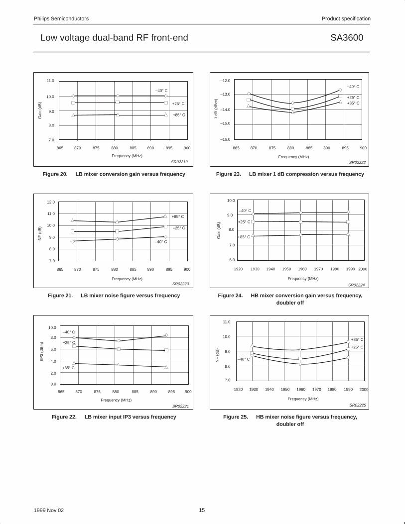
Figure 20. LB mixer conversion gain versus frequency
Frequency (MHz)
12.0
11.0
10.0
9.0
8.0
865 870 875 880 885 890 895 900
NF
(dB
)
SR02220
+25° C
+85° C
–40° C
7.0
Figure 21. LB mixer noise figure versus frequency
Frequency (MHz)
10.0
8.0
6.0
4.0
SR02221
+25° C
+85° C
–40° C
IIP3
(dB
m)
2.0
0.0
865 870 875 880 885 890 895 900
Figure 22. LB mixer input IP3 versus frequency
Frequency (MHz)
–12.0
–13.0
–14.0
–15.0
–16.0
865 870 875 880 885 890 895 900
1 dB
(dB
m)
SR02222
+25° C+85° C
–40° C
Figure 23. LB mixer 1 dB compression versus frequency
Frequency (MHz)
10.0
8.0
7.0
6.0
1920 1930 1940 1950 1960 1970 1980 1990 2000
SR02224
+25° C
+85° C
–40° C
Gai
n (d
B)
9.0
Figure 24. HB mixer conversion gain versus frequency,doubler off
Frequency (MHz)
11.0
10.0
9.0
8.0
7.0
1920 1930 1940 1950 1960 1970 1980 1990 2000
NF
(dB
)
SR02225
+25° C
+85° C
–40° C
Figure 25. HB mixer noise figure versus frequency,doubler off
Philips Semiconductors Product specification
SA3600Low voltage dual-band RF front-end
1999 Nov 02 16
Frequency (MHz)
IIP3
(dB
m)
10.0
4.0
2.0
0.0
SR02226
+25° C
+85° C
–40° C
1920 1930 1940 1950 1960 1970 1980 1990 2000
8.0
6.0
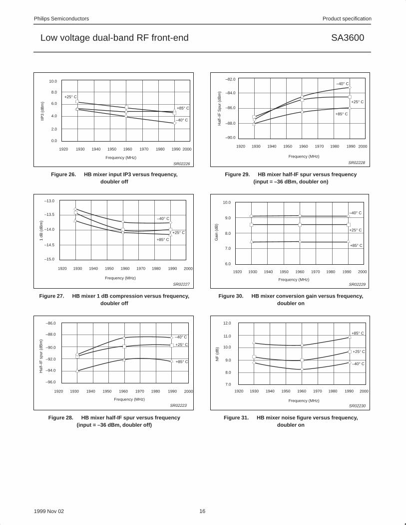
Figure 26. HB mixer input IP3 versus frequency,doubler off
Frequency (MHz)
–13.0
–13.5
–14.0
–14.5
–15.0
1920 1930 1940 1950 1960 1970 1980 1990 2000
1 dB
(dB
m)
SR02227
+25° C
+85° C
–40° C
Figure 27. HB mixer 1 dB compression versus frequency,doubler off
Frequency (MHz)
Hal
f–IF
spu
r (d
Bm
)
–86.0
–88.0
–90.0
–92.0
1920 1930 1940 1950 1960 1970 1980 1990 2000
SR02223
+25° C
+85° C
–40° C
–94.0
–96.0
Figure 28. HB mixer half-IF spur versus frequency(input = –36 dBm, doubler off)
Frequency (MHz)
–82.0
–84.0
–86.0
–88.0
–90.0
1920 1930 1940 1950 1960 1970 1980 1990 2000
Hal
f–IF
Spu
r (d
Bm
)
SR02228
+25° C
+85° C
–40° C
Figure 29. HB mixer half-IF spur versus frequency(input = –36 dBm, doubler on)
Frequency (MHz)
10.0
9.0
8.0
7.0
6.0
Gai
n (d
B)
SR02229
+25° C
+85° C
–40° C
1920 1930 1940 1950 1960 1970 1980 1990 2000
Figure 30. HB mixer conversion gain versus frequency,doubler on
Frequency (MHz)
12.0
11.0
10.0
9.0
8.0
1920 1930 1940 1950 1960 1970 1980 1990 2000
NF
(dB
)
SR02230
+25° C
+85° C
–40° C
7.0
Figure 31. HB mixer noise figure versus frequency,doubler on

Philips Semiconductors Product specification
SA3600Low voltage dual-band RF front-end
1999 Nov 02 17
Frequency (MHz)
6.0
5.0
4.0
1.0
0.0
IIP3
(dB
m)
SR02231
+25° C
+85° C
–40° C
3.0
2.0
1920 1930 1940 1950 1960 1970 1980 1990 2000
Figure 32. HB mixer input IP3 versus frequency,doubler on
Frequency (MHz)
IIP2
(dB
m)
30.0
28.0
26.0
24.0
1920 1930 1940 1950 1960 1970 1980 1990 2000
+25° C
+85° C
–40° C
SR02232
Figure 33. HB mixer input IP2 versus frequency,doubler on
Frequency (MHz)
Lo o
utpu
t pow
er (
dBm
)
–5.0
–6.0
–7.0
–8.0
950 955 960 965 970 975 980
SR02233
+25° C
+85° C
–40° C
–9.0
–10.0
Figure 34. LB LO output power versus frequency (mode 010)
Frequency (MHz)
LO o
utpu
t pow
er (
dBm
)
–6.0
–7.0
–8.0
–9.0
2010 2020 2030 2040 2050 2060 2070 2080
SR02234
+25° C
+85° C
–40° C
–10.0
–11.0
Figure 35. HB LO output power versus frequency(mode 110)

Philips Semiconductors Product specification
SA3600Low voltage dual-band RF front-end
1999 Nov 02 18
SR02235
HB_LNA_OUT
GND
HB_LNA_IN
VCC
HB_MXR+_IN
HB_MXR–_IN
PD1
GND
HB_VCO_OUT
PD2
GND
LB_LNA_OUT
GND
LB_LNA_IN
VCC
LB_MXR_IN
GND
MXR+_OUT
GND
MXR–_OUT
LB_VCO_IN
PD3
HB_VCO_INLB_VCO_OUT
1
2
3
4
5
6
7
8
9
10
11
12 13
14
15
16
17
18
19
20
21
22
23
24
PMU
PMU
10 kΩ
0.01 µF
220 pF
RFSource
10 kΩ
PMU100 pF
PMU10 kΩ
100 pF
220 pF 220 pF
5.6 nh
3 dB Pad
PMU1 kΩ
0.1 pF
PMU
100 pF
220 pF
10 nh
RF Meas.
0.1 µF
PMU1 kΩ
4.7 nh100 pF
PMU10 kΩ
RF Meas.
PMU
10 nh220 pF 1.8 pF
6.8 pF
PMU10 kΩ
RF Source
PMU0.01 µF100 pF
12 nh
PMU10 kΩ
3 dB Pad
220 pF10 nh
18 nh
470 nh8.2 pF
8.2 pF 10 pF
470 nh
RF Meas.
PMU100 pF 0.01 µF
RF Source
PMU10 kΩ
18 pF
4.7 nh
0.1 µF
1 kPMU
2.7 pF
RF Source
PMU10 kΩ
Figure 36. SA3600 production test circuit schematic

Philips Semiconductors Product specification
SA3600Low voltage dual-band RF front-end
1999 Nov 02 19
SR02236
LBLNA_OUT
GND
LBLNA_IN
VCC
LBMIX_IN
GND
MIXER_OUT-P
GND
LBVCO_IN
PD3
HBVCO_IN
HBLNA_OUT
GND
HBLNA_IN
VCC
HBMIX_IN-P
HBMIX_IN-N
PD1
GND
HBVCO_OUT
PD2
GND
LBVCO_OUTx2
1
2
3
4
5
6
7
8
9
10
11
12 13
14
15
16
17
18
19
20
21
22
23
24
L12UL
R410k
R11000
L19UL
R9UL
L18TOKO 8.2nH
R8330
R1010
C3710nF
J1SMA
J2SMA
J3SMA
J4SMA
J5SMA
J12VCC
SA3600
J11SMA
J6SMA
J7SMA
J8SMA
82MHz IFJ9
SMA
J10SMA
HBLOUT
HBLIN
HBMIN
HBLOOUT
LBLOOUT
VCC
GND R610
C26100nF
C25100pF
C38100pF
PD3
C302.2pF
L9120nHC27
6.8pFC21100pF
L132.7nH
C318.2pF0402
MIXER_OUT-N
C328.2pF0402
C23100pF
R310k
L6180nH
L7180nH
L8120nH
MIXOUT
C221nF
C2027pF
C286.8pF
C331pF
C181nF
LBMIN
LBLIN
LBLOUT
C1927pF
C121.5pF
L168.2nH
C13100pF
C3410nF
R210
C16100pF
C16100nF
L1522nH
C111.2pF
C105.6pF
R710
C2422pFL10
10nH
Tx mode, LO LB BufferRx mode cell, LO GainRx mode cell, HI Gain
Rx mode PCS, HI Gain X2Rx mode PCS, LO Gain X2
Rx mode PCS, HI Gain No X2Rx mode PCS, LO Gain No X2
Sleep mode
Mode Select PD1 PD2 PD3
00001111
00110011
01010101
PD2
PD1
L11UL
L22.7nH
L51.8nH
L32.7nH
R110
R12000
C3100nF
C4100pF
C10.5pF
C2100pF
L41.8nH
C5100pF
C61.8pF
C6100pF
C71.8pF
C9100pF
Figure 37. SA3600 Application circuit (f IF = 82 MHz)

Philips Semiconductors Product specification
SA3600Low voltage dual-band RF front-end
1999 Nov 02 20
Table 1. Low-band LNA S-parameters (high gain mode)
Freq (MHz) |S11| (U) <S11 (deg) |S21| (U) <S21 (deg) |S12| (U) <S12 (deg) |S22| (U) <S22 (deg)
800 0.42 –89 5.19 89 0.006 14 0.98 –37
810 0.42 –89 5.17 89 0.006 19 0.98 –37
820 0.41 –90 5.11 88 0.005 45 0.98 –38
830 0.41 –91 5.11 87 0.004 11 0.98 –38
840 0.41 –91 5.03 86 0.008 14 0.98 –38
850 0.41 –92 4.97 85 0.007 –2 0.98 –39
860 0.40 –92 4.97 84 0.006 32 0.98 –40
870 0.40 –93 4.92 83 0.008 8 0.98 –40
880 0.40 –93 4.85 82 0.007 –9 0.98 –41
890 0.39 –93 4.84 81 0.006 –18 0.98 –42
900 0.39 –93 4.77 81 0.005 3 0.98 –42
910 0.39 –94 4.73 79 0.005 –12 0.97 –42
920 0.38 –94 4.67 79 0.009 3 0.98 –43
930 0.38 –94 4.61 78 0.007 13 0.98 –43
940 0.38 –95 4.55 77 0.003 –1 0.98 –44
950 0.37 –95 4.49 77 0.006 –33 0.98 –44
960 0.37 –95 4.43 76 0.005 –29 0.98 –44
970 0.37 –96 4.36 75 0.008 –46 0.98 –45
980 0.36 –96 4.30 75 0.006 8 0.97 –46
990 0.36 –96 4.25 74 0.009 –24 0.98 –47
1000 0.36 –97 4.23 74 0.005 21 0.98 –47
1010 0.36 –96 4.16 73 0.007 –8 0.98 –47
1020 0.36 –97 4.15 73 0.008 –20 0.98 –48
1030 0.36 –97 4.11 73 0.008 –22 0.97 –48
1040 0.35 –97 4.07 71 0.007 –55 0.97 –49
1050 0.35 –97 4.04 71 0.009 –35 0.98 –49

Philips Semiconductors Product specification
SA3600Low voltage dual-band RF front-end
1999 Nov 02 21
Table 2. Low-band LO input (pin 15) and output (pin 12) S-parameters
Freq(MHz) |S11| (U) <S11 (deg) |S22| (U) <S22 (deg)
670 0.37 –168 0.46 75
680 0.37 –168 0.47 73
690 0.35 –169 0.49 71
700 0.33 –171 0.50 69
710 0.32 –171 0.50 67
720 0.31 –171 0.51 66
730 0.30 –172 0.52 64
740 0.28 –171 0.53 63
750 0.27 –171 0.53 61
760 0.26 –170 0.54 60
770 0.25 –170 0.55 58
780 0.24 –168 0.56 56
790 0.23 –168 0.56 55
800 0.22 –165 0.58 54
810 0.21 –162 0.58 52
820 0.20 –160 0.59 51
830 0.20 –157 0.59 49
840 0.21 –153 0.60 48
850 0.21 –149 0.60 46
860 0.20 –147 0.61 45
870 0.21 –145 0.62 44
880 0.22 –141 0.62 42
890 0.23 –140 0.62 41
900 0.24 –137 0.63 40
910 0.25 –136 0.64 38
920 0.26 –136 0.64 37
930 0.27 –134 0.64 35
940 0.29 –134 0.65 35
950 0.30 –135 0.65 33
960 0.31 –134 0.65 32
970 0.32 –134 0.65 31
980 0.34 –135 0.66 30
990 0.35 –136 0.66 29
1000 0.37 –136 0.66 28
1010 0.38 –137 0.66 26
1020 0.39 –138 0.66 26
1030 0.41 –139 0.66 25
1040 0.42 –140 0.66 24
1050 0.43 –141 0.67 23
1060 0.44 –142 0.66 22

Philips Semiconductors Product specification
SA3600Low voltage dual-band RF front-end
1999 Nov 02 22
Table 2. Low-band LO input (pin 15) and output (pin 12) S-parameters (continued)
Freq(MHz) |S11| (U) <S11 (deg) |S22| (U) <S22 (deg)
1070 0.46 –143 0.66 21
1080 0.48 –144 0.66 21
1090 0.49 –145 0.66 20
1100 0.51 –147 0.66 20
1110 0.52 –150 0.67 19
1120 0.53 –151 0.67 18
1130 0.53 –153 0.67 18
1140 0.54 –155 0.67 18
1150 0.55 –156 0.68 17
1160 0.56 –157 0.68 16
1170 0.57 –159 0.68 16

Philips Semiconductors Product specification
SA3600Low voltage dual-band RF front-end
1999 Nov 02 23
Table 3. Mixer output S-parameters
Both pins (17, 18)
Freq(MHz) |S11| (U) <S11 (deg)
70 1.00 –8
80 1.00 –9
90 0.99 –10
100 0.99 –11
110 0.99 –12
120 0.99 –13
130 0.99 –14
140 0.99 –16
150 0.99 –16
160 0.99 –18
170 0.99 –19
180 0.99 –20
190 0.99 –21
200 0.99 –22

Philips Semiconductors Product specification
SA3600Low voltage dual-band RF front-end
1999 Nov 02 24
Table 4. Low-band mixer input S-parameters
Freq(MHz) |S11| (U) <S11 (deg)
800 0.84 –14
810 0.85 –14
820 0.85 –14
830 0.85 –15
840 0.84 –15
850 0.85 –15
860 0.85 –15
870 0.84 –15
880 0.85 –15
890 0.85 –15
900 0.84 –16
910 0.85 –15
920 0.84 –16
930 0.85 –16
940 0.85 –17
950 0.85 –17
960 0.85 –17
970 0.84 –17
980 0.85 –17
990 0.84 –18
1000 0.84 –18
1010 0.85 –18
1020 0.84 –18
1030 0.85 –19
1040 0.84 –19
1050 0.85 –19

Philips Semiconductors Product specification
SA3600Low voltage dual-band RF front-end
1999 Nov 02 25
Table 5. High-band LNA S-parameters
Freq (MHz) |S11| (U) <S11 (deg) |S21| (U) <S21 (deg) |S12| (U) <S12 (deg) |S22| (U) <S22 (deg)
1800 0.38 156 6.73 172 0.05 105 0.13 –106
1810 0.37 156 6.77 170 0.05 113 0.11 –100
1820 0.37 155 6.82 168 0.05 109 0.10 –95
1830 0.37 154 6.79 167 0.05 107 0.10 –88
1840 0.36 155 6.84 165 0.05 106 0.09 –74
1850 0.36 154 6.80 164 0.05 102 0.09 –67
1860 0.35 155 6.81 162 0.05 108 0.10 –51
1870 0.35 154 6.85 161 0.05 101 0.10 –47
1880 0.34 152 6.84 159 0.05 102 0.12 –41
1890 0.33 154 6.84 158 0.05 107 0.13 –36
1900 0.33 153 6.83 157 0.05 102 0.14 –32
1910 0.33 154 6.83 155 0.05 101 0.15 –30
1920 0.32 153 6.87 154 0.05 102 0.17 –28
1930 0.32 154 6.84 152 0.05 99 0.18 –28
1940 0.32 153 6.86 151 0.05 101 0.19 –26
1950 0.32 153 6.84 149 0.05 103 0.21 –26
1960 0.32 154 6.78 148 0.05 101 0.22 –26
1970 0.32 155 6.80 146 0.05 100 0.24 –26
1980 0.31 154 6.75 145 0.04 100 0.26 –26
1990 0.32 156 6.72 143 0.04 99 0.27 –27
2000 0.31 155 6.68 142 0.05 100 0.28 –27
2010 0.31 156 6.68 141 0.05 103 0.30 –30
2020 0.31 157 6.65 139 0.04 104 0.31 –31
2030 0.31 158 6.63 138 0.04 96 0.32 –30
2040 0.31 158 6.59 137 0.05 105 0.33 –32
2050 0.31 159 6.58 135 0.05 104 0.34 –34

Philips Semiconductors Product specification
SA3600Low voltage dual-band RF front-end
1999 Nov 02 26
Table 6. High-band LO input (pin 13) and output (pin 9) S-parameters
Freq(MHz) |S11| (U) <S11 (deg) |S22| (U) <S22 (deg)
1700 0.82 –36 0.31 86
1710 0.82 –36 0.30 85
1720 0.82 –37 0.29 83
1730 0.82 –36 0.29 81
1740 0.82 –37 0.29 81
1750 0.83 –37 0.27 79
1760 0.82 –37 0.26 76
1770 0.82 –38 0.25 76
1780 0.82 –38 0.24 74
1790 0.83 –39 0.24 72
1800 0.82 –39 0.23 71
1810 0.82 –39 0.21 69
1820 0.83 –40 0.20 68
1830 0.82 –40 0.20 66
1840 0.82 –41 0.18 67
1850 0.82 –41 0.16 63
1860 0.82 –42 0.16 61
1870 0.82 –42 0.14 60
1880 0.82 –42 0.12 56
1890 0.82 –43 0.11 52
1900 0.82 –43 0.11 53
1910 0.81 –44 0.08 47
1920 0.82 –44 0.07 42
1930 0.81 –45 0.06 34
1940 0.81 –46 0.04 29
1950 0.81 –46 0.03 –1
1960 0.81 –47 0.02 –21
1970 0.80 –47 0.03 –57
1980 0.80 –48 0.04 –85
1990 0.80 –48 0.05 –103
2000 0.80 –48 0.07 –112
2010 0.80 –49 0.08 –112
2020 0.80 –50 0.10 –119
2030 0.80 –51 0.12 –120
2040 0.79 –51 0.13 –125
2050 0.79 –52 0.15 –127
2060 0.79 –52 0.16 –130
2070 0.79 –52 0.18 –133
2080 0.78 –53 0.20 –135
2090 0.77 –54 0.21 –136

Philips Semiconductors Product specification
SA3600Low voltage dual-band RF front-end
1999 Nov 02 27
Table 6. High-band LO input (pin 13) and output (pin 9) S-parameters (continued)
Freq(MHz) |S11| (U) <S11 (deg) |S22| (U) <S22 (deg)
2100 0.78 –54 0.23 –138
2110 0.77 –55 0.24 –139
2120 0.77 –56 0.26 –142
2130 0.77 –57 0.27 –144
2140 0.76 –57 0.29 –144
2150 0.77 –58 0.29 –145
2160 0.76 –58 0.31 –147
2170 0.76 –59 0.33 –148
2180 0.76 –60 0.34 –150
2190 0.76 –60 0.35 –150
2200 0.76 –61 0.36 –152

Philips Semiconductors Product specification
SA3600Low voltage dual-band RF front-end
1999 Nov 02 28
TSSOP24: plastic thin shrink small outline package; 24 leads; body width 4.4 mm SOT355-1

Philips Semiconductors Product specification
SA3600Low voltage dual-band RF front-end
1999 Nov 02 29
NOTES

Philips Semiconductors Product specification
SA3600Low voltage dual-band RF front-end
1999 Nov 02 30
DefinitionsShort-form specification — The data in a short-form specification is extracted from a full data sheet with the same type number and title. Fordetailed information see the relevant data sheet or data handbook.
Limiting values definition — Limiting values given are in accordance with the Absolute Maximum Rating System (IEC 134). Stress above oneor more of the limiting values may cause permanent damage to the device. These are stress ratings only and operation of the device at these orat any other conditions above those given in the Characteristics sections of the specification is not implied. Exposure to limiting values for extendedperiods may affect device reliability.
Application information — Applications that are described herein for any of these products are for illustrative purposes only. PhilipsSemiconductors make no representation or warranty that such applications will be suitable for the specified use without further testing ormodification.
DisclaimersLife support — These products are not designed for use in life support appliances, devices or systems where malfunction of these products canreasonably be expected to result in personal injury. Philips Semiconductors customers using or selling these products for use in such applicationsdo so at their own risk and agree to fully indemnify Philips Semiconductors for any damages resulting from such application.
Right to make changes — Philips Semiconductors reserves the right to make changes, without notice, in the products, including circuits, standardcells, and/or software, described or contained herein in order to improve design and/or performance. Philips Semiconductors assumes noresponsibility or liability for the use of any of these products, conveys no license or title under any patent, copyright, or mask work right to theseproducts, and makes no representations or warranties that these products are free from patent, copyright, or mask work right infringement, unlessotherwise specified.
Philips Semiconductors811 East Arques AvenueP.O. Box 3409Sunnyvale, California 94088–3409Telephone 800-234-7381
Copyright Philips Electronics North America Corporation 1999All rights reserved. Printed in U.S.A.
Date of release: 11-99
Document order number: 9397-750-06558
Data sheetstatus
Objective specification
Preliminary specification
Product specification
Productstatus
Development
Qualification
Production
Definition [1]
This data sheet contains the design target or goal specifications for product development.Specification may change in any manner without notice.
This data sheet contains preliminary data, and supplementary data will be published at a later date.Philips Semiconductors reserves the right to make changes at any time without notice in order toimprove design and supply the best possible product.
This data sheet contains final specifications. Philips Semiconductors reserves the right to makechanges at any time without notice in order to improve design and supply the best possible product.
Data sheet status
[1] Please consult the most recently issued datasheet before initiating or completing a design.

This datasheet has been download from:
www.datasheetcatalog.com
Datasheets for electronics components.


![Atmel ATmega16U4, ATmega32U4 Datasheet …...ATmega16U4/32U4 [DATASHEET] 8](https://img.pdfslide.net/doc/110x75/5f0a39897e708231d42a9d86/-atmel-atmega16u4-atmega32u4-datasheet-atmega16u432u4-datasheet-8.jpg)