Embed Size (px)
Citation preview

SMART ARM-based Microcontrollers
SAME70-XPLD
USER GUIDE
Preface
The Atmelreg SAM E70 Xplained evaluation kit is a hardware platform toevaluate the Atmel ATSAME70Q21 microcontroller
Supported by the Atmel Studio integrated development platform the kitprovides easy access to the features of the ATSAME70Q21 and explainshow to integrate the device in a custom design
The Xplained Pro MCU series evaluation kits include an on-boardEmbedded Debugger and no external tools are necessary to program ordebug the ATSAME70Q21
The Xplained Pro extension series evaluation kits offers additionalperipherals to extend the features of the board and ease the development ofcustom designs
Atmel-44050A-SAME70-XPLD_User Guide-122015
Table of Contents
Preface 1
1 Introduction311 Kit Contents312 Related Items 313 Kit Overview 3
2 Getting Started621 Xplained Pro Quick Start 622 Design documentation and relevant links6
3 Xplained Pro 731 Embedded Debugger 732 Hardware Identification System733 Power Sources 834 Xplained Pro Standard Extension Header835 Xplained Pro Power Header9
4 Hardware User Guide 1141 Microcontroller 1142 Power Distribution1143 Connectors 1244 Peripherals 3045 Zero Ohm Resistors 3846 Embedded Debugger Implementation41
5 Board Schematics44
6 Board Layout 51
7 Evaluation Boardkit Important Notice 57
Atmel SAME70-XPLD [USER GUIDE]Atmel-44050A-SAME70-XPLD_User Guide-122015
2
1 IntroductionThis user guide introduces the Atmel SAME70-XPLD evaluation kit and describes the development anddebugging capabilities for applications running on a SAM E70 ARM-based embedded microcontroller
11 Kit Contentsbull Boards
ndash One SAME70-XPLD boardbull Cables
ndash One Micro-AB type USB cable
12 Related Itemsbull Atmel SAM E70 Series Datasheet
13 Kit Overview
131 Evaluation Kit ArchitectureFigure 1-1 Evaluation Kit Architecture
SDRAM16Mb SDRAM
ETHERNETEthernet 10100 InterfaceSDCARD
4-bit SDCARDReader Interface
USB DEBUGUSB Micro AB Connector
ATMEL EDBGAtmel Embedded Debugguer
JTAG20-Pin JTAG Connector
ARDUINO CONNECTORS8-Expansion Headers Arduino R3 compatible PIO Signals(Not Populated)
XPRO CONNECTORS3-Expansions HeadersCompatible with Atmel XPRO Extensions
TARGET USBUSB Micro AB Connector
CAMERA MODULECamera Interface Connector
for CAMx-EB Camera Module series(Not Populated)
TRACE20-pin debug connector
For Trace (Not Populated)
EEPROMIsup2C - 2k-bit serial EEprom
And Unique 128-bit serial numberAT24MAC402
Atmel SAME70-XPLD [USER GUIDE]Atmel-44050A-SAME70-XPLD_User Guide-122015
3
132 Evaluation Kit SpecificationsTable 1-1 Evaluation Kit Specifications
Characteristic Specifications
Temperature Operating 0degC to +70degC
Storage -40degC to +85degC
Relative Humidity 0 to 90 (non-condensing)
RoHS status Compliant
Ordering code ATSAME70-XPLD
133 Board FeaturesTable 1-2 Board Specifications
Characteristics Specifications
PCB characteristics 835 times 105 times 16mm (4 layers)
Processor ATSAME70Q21 (144-lead LQFP package) ARM Cortex-M7 Processor
Processor clock sources 12 MHz crystal oscillator32768 kHz crystal oscillator (not populated)
EEPROM One AT24MAC402 EEPROM
SDRAM One IS42S16100E 16 Mb SDRAM
SDMMC One 4-bit SD card connector
USB One Micro-AB USB deviceOne Micro-AB USB for EDBG debug interface
Camera interface Camera Extension Header for connection with ISI Modules (not populated)
Ethernet One Ethernet PHY (RMII 10100)
Debug port One JTAG interface connectorOne ETM Trace interface connector (not populated)
Expansion connectors Three Atmel XPRO Extension HeadersArduino R3 compatible set of headers (not populated)
GPIOTWI SPI USART UART and Audio interfaces are accessible via theseheaders
Board supply voltage 5V from USB target from USB Debug or from Arduino shieldOn-board power regulation is performed by a 33V LDO
User interface Reset and free user pushbuttonOne green user LED
134 Board OverviewThe Atmel SAME70-XPLD is a hardware platform to evaluate the Atmel ATSAME70Q21
Atmel SAME70-XPLD [USER GUIDE]Atmel-44050A-SAME70-XPLD_User Guide-122015
4
It offers a set of features that enables the ATSAME70Q21 user to get started with the SAM V71 SAMV70 SAM E70 and SAM S70 peripherals right away and to get an understanding of how to integrate thedevice in their own design
The SAME70-XPLD board is equipped with the interface connectors described in Table 1-3
Table 1-3 SAME70-XPLD Board Interface Connectors
Header Interfaces to
J302 USB A device Supports USB device using a Micro-AB connector
J400 Camera Interface Connector (not populated)
J401-J402 Atmel XPRO expansion connectors
J403 Connector for Trace (not populated) (Footprint available on bottom side)
J406 JTAG 20-pin connector
J500ndashJ507 Expansion connectors with Arduino R3 compatible PIO signals (not populated)
J600 SDMMC connector (available on bottom side)
J700 Ethernet ETH1
J900 Debug USB interface Supports USB device using a Micro-AB connector Interface used fortarget debug
Figure 1-2 SAME70-XPLD Board Overview
Atmel SAME70-XPLD [USER GUIDE]Atmel-44050A-SAME70-XPLD_User Guide-122015
5
2 Getting Started
21 Xplained Pro Quick StartThree steps to start exploring the Atmel Xplained Pro platform
1 Download Atmel Studio2 Launch Atmel Studio3 Connect a USB cable (Standard-A to Micro-B or Micro-AB) between the PC and the DEBUG USB
port of the board
When the Atmel SAME70-XPLD is connected to your computer for the first time the operating system willperform a driver software installation The driver file supports both 32- and 64-bit versions of Microsoftreg
Windowsreg XP Windows Vistareg Windows 7 and Windows 8
Once the board is powered Atmel Studio will auto detect which kind of MCU and extension board(s) areconnected Atmel Studio will present links to relevant information like datasheets and kit documentationThe kit landing page in Atmel Studio also has the option to launch Atmel Software Framework (ASF)example applications for the kit The SAM E70 device is programmed and debugged by the on-boardEmbedded Debugger and therefore no external programmer or debugger tool is needed
22 Design documentation and relevant linksThe following list contains links to the most relevant documents and software for SAME70-XPLD
bull Xplained Pro products - Atmel Xplained Pro is a series of small-sized and easy-to-use evaluationkits for Atmel microcontrollers and other Atmel products It consists of a series of low-cost MCUboards for evaluation and demonstration of features and capabilities of different MCU families
bull Atmel Studio - Free Atmel IDE for development of CC++ and assembler code for Atmelmicrocontrollers
bull Atmel sample store - Atmel sample store where you can order samples of devicesbull EDBG User Guide - User guide containing more information about the on-board Embedded
Debuggerbull IAR Embedded Workbenchreg for ARMreg - This is a commercial CC++ compiler that is available for
ARMreg There is a 30 day evaluation version as well as a code size limited kick-start versionavailable from their website The code size limit is 16KB for devices with M0 M0+ and M1 coresand 32KB for devices with other cores
bull Atmel Data Visualizer - Atmel Data Visualizer is a program used for processing and visualizingdata Data Visualizer can receive data from various sources such as the Embedded Debugger DataGateway Interface found on Xplained Pro boards and COM ports
bull Design Documentation - Package containing schematics BOM assembly drawings 3D plotslayer plots etc
bull Hardware Users Guide in PDF format - PDF version of this User Guide
Atmel SAME70-XPLD [USER GUIDE]Atmel-44050A-SAME70-XPLD_User Guide-122015
6
3 Xplained ProXplained Pro is an evaluation platform that provides the full Atmel microcontroller experience Theplatform consists of a series of Microcontroller (MCU) boards and extension boards which are integratedwith Atmel Studio have Atmel Software Framework (ASF) drivers and demo code support datastreaming and more Xplained Pro MCU boards support a wide range of Xplained Pro extension boardswhich are connected through a set of standardized headers and connectors Each extension board hasan identification (ID) chip to uniquely identify which boards are connected to an Xplained Pro MCU boardThis information is used to present relevant user guides application notes datasheets and examplecode through Atmel Studio
31 Embedded DebuggerThe SAME70-XPLD contains the Atmel Embedded Debugger (EDBG) for on-board debugging TheEDBG is a composite USB device of three interfaces a debugger Virtual COM Port and a Data GatewayInterface (DGI)
Together with Atmel Studio the EDBG can program and debug the ATSAME70Q21 On the SAME70-XPLD the SWD interface is connected between the EDBG and the ATSAME70Q21
The Virtual COM Port is connected to a UART on the ATSAME70Q21 and provides an easy way tocommunicate with the target application through terminal software It offers variable baud rate parity andstop bit settings Note that the settings on the ATSAME70Q21 must match the settings applied in theterminal software
Note If not set automatically data terminal ready (DTR) must be set in the terminal software
The DGI consists of several physical interfaces for communication with the host computerCommunication over the interfaces are bidirectional It can be used to send events and values from theATSAME70Q21 or as a generic printf-style data channel Traffic over the interfaces can be timestampedon the EDBG for more accurate tracing of events Note that timestamping imposes an overhead thatreduces maximal throughput Atmel Data Visualizer is used to send and receive data through DGI
For further documentation on the EDBG see the EDBG User Guide
32 Hardware Identification SystemAll Xplained Pro compatible extension boards have an Atmel ATSHA204 CryptoAuthenticationtrade chipmounted This chip contains information that identifies the extension with its name and some extra dataWhen an Xplained Pro extension is connected to an Xplained Pro MCU board the information is read andsent to Atmel Studio The Atmel Kits extension installed with Atmel Studio will give relevant informationcode examples and links to relevant documents The table below shows the data fields stored in the IDchip with example content
Table 3-1 Xplained Pro ID Chip Content
Data field Data type Example content
Manufacturer ASCII string Atmel0
Product Name ASCII string Segment LCD1 Xplained Pro0
Product Revision ASCII string 020
Product Serial Number ASCII string 1774020200000010rsquo0rsquo
Atmel SAME70-XPLD [USER GUIDE]Atmel-44050A-SAME70-XPLD_User Guide-122015
7
Data field Data type Example content
Minimum Voltage [mV] uint16_t 3000
Maximum Voltage [mV] uint16_t 3600
Maximum Current [mA] uint16_t 30
33 Power SourcesThe SAME70-XPLD kit can be powered by several power sources listed in the table below
Warning The 33V power domain is locally generated and must never be supplied fromexternal sources or this would damage the on-board regulators
Table 3-2 SAME70-XPLD Power Sources
Power input Voltage requirements Connector marking
Embedded debugger USB 44V to 525V (USB spec) DEBUG USB
Target USB 44V to 525V (USB spec) TARGET USB
Arduino connector 50V typically J501 (pin 5)
In case of USB power sources the board automatically detects and switches to the available one If thetwo are present (which is no problem whatsoever) the following priority applies
1 Target USB (J302 connector)2 Embedded Debugger USB (J900 connector)
Info USB sources supposedly provide a maximum current of 500mA Calculate the powerbudget of your system there is a possiblity this could be not enough if your SAME70-XPLD alsoconnects to power demanding extension boards
The optional 5Vcc power source from the Arduino connector J501 is connected in parallel to the USBpower switching system hence the following warning
Warning do not power the board form the Arduino shield (J501) when either of the two USBsources are connected Doing so could damage the board and potentially also damage the USBport of your PC
34 Xplained Pro Standard Extension HeaderAll Xplained Pro kits have one or more dual row 20-pin 100mil extension header Xplained Pro MCUboards have male headers while Xplained Pro extensions have their female counterparts Note that allpins are not always connected All connected pins follow the defined pin-out description in the tablebelow
Atmel SAME70-XPLD [USER GUIDE]Atmel-44050A-SAME70-XPLD_User Guide-122015
8
The extension headers can be used to connect a variety of Xplained Pro extensions to Xplained Pro MCUboards or to access the pins of the target MCU on Xplained Pro MCU boards directly
Table 3-3 Xplained Pro Standard Extension Header
Pin number Name Description
1 ID Communication line to the ID chip on an extension board
2 GND Ground
3 ADC(+) Analog to digital converter alternatively positive part of differentialADC
4 ADC(-) Analog to digital converter alternatively negative part of differentialADC
5 GPIO1 General purpose IO
6 GPIO2 General purpose IO
7 PWM(+) Pulse width modulation alternatively positive part of differentialPWM
8 PWM(-) Pulse width modulation alternatively negative part of differentialPWM
9 IRQGPIO Interrupt request line andor general purpose IO
10 SPI_SS_BGPIO
Slave select for SPI andor general purpose IO
11 I2C_SDA Data line for I2C interface Always implemented bus type
12 I2C_SCL Clock line for I2C interface Always implemented bus type
13 UART_RX Receiver line of target device UART
14 UART_TX Transmitter line of target device UART
15 SPI_SS_A Slave select for SPI Should preferably be unique
16 SPI_MOSI Master out slave in line of serial peripheral interface Alwaysimplemented bus type
17 SPI_MISO Master in slave out line of serial peripheral interface Alwaysimplemented bus type
18 SPI_SCK Clock for serial peripheral interface Always implemented bus type
19 GND Ground
20 VCC Power for extension board
35 Xplained Pro Power HeaderThe power header can only be used as supply for external peripherals or extension boards Care must betaken not to exceed the total current limitation of the on-board regulator when using the 33V pin
Atmel SAME70-XPLD [USER GUIDE]Atmel-44050A-SAME70-XPLD_User Guide-122015
9
Table 3-4 Xplained Pro Power Header
Pin number Pin name Description
1 na not connected
2 GND Ground
3 VCC_5V0 Output unregulated 5V (output derived from one of the inputsources)
4 VCC_3V3 Output regulated 33V (output used as main power supply for thekit)
Atmel SAME70-XPLD [USER GUIDE]Atmel-44050A-SAME70-XPLD_User Guide-122015
10
4 Hardware User Guide
41 MicrocontrollerThe SAME70-XPLD board is built around the ATSAME70Q21 in a 144-lead LQFP package It is a low-power ARM Cortex-M7 application microcontroller achieving high-performance computing device andembedding a wide range of communication peripherals It features a combination of user interfacefunctionalities and high data rate IOs camera interface 10100 Ethernet ports high-speed USB and SDCard
The ARM Cortex-M7 processor supports SDRAM memory through an EBI interface An internal 150 MHzmulti-layer AHB bus architecture associated with 24 XDMA channels 384 Kbytes of SRAM and 2048Kbytes of Flash sustains the high bandwidth required by the microcontroller and the high-speedperipherals
Figure 4-1 SAM E70 Block Diagram
12-layer Bus Matrix fMAX 150 MHz
XDMA
PCK02
XIN32XOUT32
ERASE
VDDCORE
VDDIOVDDOUT
VoltageRegulator
TST
WKUP013
VDDIO
XINXOUT
VDDPLL
RTCOUT0RTCOUT1
S M MMMSS S S
S
MM
M
M
M
S
System Controller
SM
In-Circuit Emulator
MPU
Cortex-M7 ProcessorfMAX 300 MHzNVIC
FPU
TPIU
ETM
16 Kbytes ICache + ECC16 Kbytes DCache + ECC
TCMInterface
AXIMAHBP AHBS
AXI Bridge
TCKSWCLK
TDITDOTRACESWO
JTAGSEL
Serial Wire DebugJTAG Boundary Scan
TRACECLK
TRACED03
TMSSWDIO
NRST
PIOABCDE
24-channelXDMA
ROM
Boot Program
Multi-portSRAM
Flash2048 Kbytes1024 Kbytes512 Kbytes
FlashUnique ID
ITCM
DTCM USBHS
Transceiver
External Bus Interface Static Memory Controller (SMC)SDRAM Controller (SDRAMC)
NAND Flash Logic
QSPI
XIP DMA
ISI GMACMIIRMII
5 xUART
3 xTWIHS
3 xUSART
2 xPWM
2 x12-bit AFE ACC 12-bit
DACPIO SSC HSMCI 2 x
SPI4 x TC
XDMA
DMA
Peripheral Bridge
URXD04
UTXD04
VREFN
CANRX01
CANTX01
RXD02
SCK02
RTS02
TXD02
CTS02
DSR02 D
TR02
RI02 D
CD02
ICMSHA
PIODCCLK
PIODCEN12
PIODC07 TFTKTD RD RK RF
MCDA03
MCCDAMCCK
SPIx_NPCS03
SPIx_MISO
SPIx_MOSI
SPIx_SPCK
PWMCx_PWMH03
PWMCx_PWML03
PWMCx_PWMFI02
PWMCx_PWMEXTRG01
AFEx_ADTRG
AFEx_AD01
1
DAC01
DATRG
TWD02
TWCK02
2 x MCAN
GTXCK GRXCK G
REFCK
GCRS GCOL G
CRSDV
GMDC GMDIO
GTSUCOMP
GRX03 G
TX03
GRXER GRXDV
GTXER GTXDV
ISI_D[110]
ISI_PCK ISI_MCK
ISI_HSYNC ISI_VSYNC
HSDPHSDM
QMISOQIO
1
QMOSIQIO
0
QSCK QCS
QIO23
A[230] D[150]
A21NANDALE
A22NANDCLE
NANDOE NANDWE
A0NLB N
UB
NWAIT N
CS03 N
RD NWE
A16SDBA0 A17SDBA1
RAS CAS D
QM01 S
DCK SDCKE S
DA10
DMA DMA
Temp Sensor
TIOB01
1
TCLK011
TIOA01
1
XDMAXDMAXDMAXDMAXDMAXDMAXDMAXDMAXDMA
XDMA
FIFO
XDMA
TRNGAES
DMA
VREFP
Backup RAM1 Kbyte
TCM SRAM
System RAM
0ndash256 Kbytes
128ndash384 Kbytes0ndash256 Kbytes
PMC4812 MHz
RC Oscillator
RSTC
SM
POR
SUPC
RTTRTC
WDT
UPLL
PLLA
3-20 MHzCrystal
Oscillator
32 kHzCrystal
Oscillator
32 kHzRC Oscillator
Immediate Clear256-bit SRAM
(GPBR)
Backup
RSWDT
42 Power DistributionThe SAME70-XPLD has two power sources as described in the figure Power Supply Block Diagram
The kit can be powered from the EDBG USB or from the target USB The kit automatically selects asource to draw power Priority is given to TARGET USB power input
Atmel SAME70-XPLD [USER GUIDE]Atmel-44050A-SAME70-XPLD_User Guide-122015
11
Figure 4-2 Power Supply Block Diagram
Coin Cell
TARGET USB
EDBG USB
VCC_5V0
43 ConnectorsThese sections describe the implementation of all connectors and headers on SAME70-XPLD and theirconnection to the ATSAME70Q21 The tables of connections in these sections also describe whichsignals are shared between the headers and on-board functionality The figure below shows all availableconnectors and jumpers on the SAME70-XPLD
Figure 4-3 SAME70-XPLD Connector Overview
J406
- SA
ME7
0 De
bug
(SW
D)
CAMERAINTERFACE
J600 - SDCARD Socket(Bottom Side)
J900DEBUG USB
Coresight 20 - SWD + ETM(Bottom Side)
J506 - SPI
J504
- An
alog
Hig
hJ5
02 -
Anal
og Lo
wJ5
01 -
Pow
er
J500
- Di
gita
l Hig
hJ5
03 -
Digi
tal L
owJ5
05 -
Com
mun
icat
ion
J402
- Ex
tens
ion
Head
er 2
J401
- Ex
tens
ion
Head
er 1
J101
- Po
wer
Hea
der
VDDCORE VCC_MCU_3V3
J200 - ERASE
J700 - Ethernet RJ45
J507 - Digital Extra
J302
Targ
et U
SB
OPT
ION
OPT
ION
OPT
ION O
PTIO
NO
PTIO
NO
PTIO
N
OPTION
OPTION
OPTION
Atmel SAME70-XPLD [USER GUIDE]Atmel-44050A-SAME70-XPLD_User Guide-122015
12
431 Extension HeadersThe Xplained Pro headers EXT1 and EXT2 on SAME70-XPLD give access to the IO of themicrocontroller in order to expand the system eg by connecting extensions boards The headers have apitch of 254mm
Table 4-1 EXT1 Header
EXT1 Pin SAM E70Pin
Function Shared Functionality
1 [ID ] -- ID_EXT1 Signal connected to Embedded Debugger
2 [GND] -- -- Ground Connection with Extension Board
3 [ADC(+)] PC31 AFE1_AD6 J502 Header amp J504 Header (Arduino Shield)
4 [ADC(-)] PA19 AFE0_AD8 J502 Header (Arduino Shield)
5 [GPIO1] PB3 GPIORTS0 Camera Connector EXT2 Header J504 Header amp J507 Header (Arduino Shield)
6 [GPIO2] PB2 GPIOCTS0 EXT2 Header J504 Header amp J507 Header(Arduino Shield)
7 [PWM(+)] PA0 PWMC0_H0 --
8 [PWM(-)] PC30 TIOB5 J502 Header (Arduino Shield)
9 [IRQGPIO] PD28 WKUP5 Camera Connector Embedded Debugger J503Header amp J505 Header (Arduino Shield)
10 [SPI_SS_BGPIO] PC17 GPIO --
11 [I2C_SDA] PA3 TWD0 Camera Connector EXT2 Header J500 Header (Arduino Shield) AT24MAC402 EmbeddedDebugger
12 [I2C_SCL] PA4 TWCK0 Camera Connector EXT2 Header J500 Header (Arduino Shield) AT24MAC402 EmbeddedDebugger
13 [UART_RX] PB0 RXD0 EXT2 Header J505 Header amp J507 Header(Arduino Shield)
14 [UART_TX] PB1 TXD0 EXT2 Header J505 Header amp J507 Header(Arduino Shield)
15 [SPI_SS_A] PD25 SPI0_NPCS1 Camera Connector J500 Header (Arduino Shield)
16 [SPI_MOSI] PD21 SPI0_MOSI EXT2 Header Camera Connector J500 Header amp J506 Header (Arduino Shield) EmbeddedDebugger
17 [SPI_MISO] PD20 SPI0_MISO EXT2 Header J500 Header amp J506 Header(Arduino Shield) Embedded Debugger
18 [SPI_SCK PD22 SPI0_SPCK EXT2 Header Camera Connector J500 Header amp J506 Header (Arduino Shield) EmbeddedDebugger
Atmel SAME70-XPLD [USER GUIDE]Atmel-44050A-SAME70-XPLD_User Guide-122015
13
EXT1 Pin SAM E70Pin
Function Shared Functionality
19 [GND] -- -- Ground Connection with Extension Board
20 [VCC] -- -- Power For Extension Board (33V only)
Table 4-2 EXT2 Header
EXT2 Pin SAM E70Pin
Function Shared Functionality
1 [ID ] -- ID_EXT2 Signal connected to EmbeddedDebugger
2 [GND] -- -- Ground Connection with ExtensionBoard
3 [ADC(+)] PD30 AFE0_AD0 Camera Connector J502 Header amp J503 Header (Arduino Shield)
4 [ADC(-)] PC13 AFE1_AD1 J502 Header (Arduino Shield)
5 [GPIO1] PA6 GPIO Camera Connector J503 Header (Arduino Shield)
6 [GPIO2] PD11 GPIO Camera Connector J500 Header amp J503 Header (Arduino Shield)
7 [PWM(+)] PC19 PWMC0_H2 Camera Connector J503 Header (Arduino Shield)
8 [PWM(-)] PD26 PWMC0_L2 J502 Header (Arduino Shield)
9 [IRQGPIO] PA2 WKUP2 J503 Header (Arduino Shield) Embedded Debugger
10 [SPI_SS_BGPIO]
PA24 GPIO Camera Connector J507 Header (Arduino Shield)
11 [I2C_SDA] PA3 TWD0 Camera Connector EXT1 Header J500 Header (Arduino Shield) AT24MAC402 Embedded Debugger
12 [I2C_SCL] PA4 TWCK0 Camera Connector EXT1 Header J500 Header (Arduino Shield) AT24MAC402 Embedded Debugger
13 [UART_RX] PA21 RXD1 J507 Header (Arduino Shield) Embedded Debugger
14 [UART_TX] PB4 TXD1 J507 Header (Arduino Shield) Embedded Debugger
Atmel SAME70-XPLD [USER GUIDE]Atmel-44050A-SAME70-XPLD_User Guide-122015
14
EXT2 Pin SAM E70Pin
Function Shared Functionality
15 [SPI_SS_A] PB3 USART_SPI_NSS_MASTER_0 EXT1 Header Camera Connector J504 Header amp J507 Header (ArduinoShield)
PD31 USART_SPI_NSS_MASTER_0 Camera Connector
PB2 USART_SPI_NSS_SLAVE EXT1 Header J504 Header amp J507Header (Arduino Shield)
PD27 SPI0_NPCS3 Camera Connector J503 Header amp J505 Header (Arduino Shield)
16 [SPI_MOSI] PD21 SPI0_MOSI EXT1 Header Camera Connector J500 Header amp J506 Header (ArduinoShield) Embedded Debugger
PB1 USART_SPI_MOSI EXT1 Header J505 Header amp J507Header (Arduino Shield)
17 [SPI_MISO] PD20 SPI0_MISO EXT1 Header J500 Header amp J506Header (Arduino Shield) EmbeddedDebugger
PB0 USART_SPI_MOSI EXT1 Header J505 Header amp J507Header (Arduino Shield)
18 [SPI_SCK PD22 SPI0_SPCK EXT1 Header Camera Connector J500 Header amp J506 Header (ArduinoShield) Embedded Debugger
PB13 USART_SPI_SPCK J504 Header amp J507 Header (ArduinoShield)
19 [GND] -- -- Ground Connection with ExtensionBoard
20 [VCC] -- -- Power For Extension Board (33V only)
432 Arduino ConnectorsFive 8-pin one 10-pin one 2times3-pin and one 2times18-pin headers footprints (J500 to J507) are implementedon the board to enable the addition of Arduino shields extension cards These accessory boards arevarious and widely available on the market often custom developed Due to the PIO multiplexing of theATSAME70Q21 various peripheral signals may be connected to each pin These connectors aremechanically (location and footprint) compatible with the Arduino R3 shields
Important As the SAM E70 signals have a voltage level of 33V 5V level shields cannotproperly function with SAME70-XPLD
In addition to its standard IO functionality the SAM E70 microcontroller can provide alternate functions toexternal IO lines available on the J500 to J507 headers
These alternate functions are
Atmel SAME70-XPLD [USER GUIDE]Atmel-44050A-SAME70-XPLD_User Guide-122015
15
bull UARTs UART1 UART2 UART3 UART4bull USARTs USART0 USART1 USART2bull SPI SPI0bull Isup2C TWI0 TWI2bull Timer capture and compare TIOA[0 211] TIOB[5 7 811] TCLK[1 2 5 811]bull Clock out PCK0 PCK1 PCK2bull PWMs PWMC0_PWMEXTRG[01] PWMC0_PWMH[03] PWMC_PWML[0 2 3]
PWMC1_PWMEXTRG[01] PWMC1_PWMFI[02] PWMC1_PWMH[0 2] PWMC1_PWML[03]bull DIGITAL AUDIO TD TK TF RD RK RF GTSUCOMPbull CAN CANRX0 CANTX0 CANRX1 CANTX1bull Analog ADVREF AFE0_AD[0 6 8] AFE1_AD[1 3 5 6] DAC[01]bull GPIO MISCbull RESET
Refer to the SAM E70 Series datasheet for further details on the PIO multiplexing and alternate functionselection
Caution Like the Arduino Due SAME70-XPLD runs at 33V and the maximum voltage thatthe IO pins can tolerate is 33V connecting higher voltages eg 5V to those IO pin coulddamage the board
Important not all pins of the shield connectors are necessarily connected to an IO of theATSAME70Q21 Each shield should be checked for compatibility against the SAME70-XPLDschematics before it is purchased and connected
4321 J500 HeaderJ500 is a 10-pin header with 254mm pitch It is not populated by default and can be used to connect toArduino Shields It includes PWM Timer Counter and I2C interface signals and analog reference
Atmel SAME70-XPLD [USER GUIDE]Atmel-44050A-SAME70-XPLD_User Guide-122015
16
Figure 4-4 J500 Header
J406
- SA
ME7
0 De
bug
(SW
D)
J600 - SDCARD Socket(Bottom Side)
J900DEBUG USB
Coresight 20 - SWD + ETM(Bottom Side)
VDDCORE VCC_MCU_3V3
J200 - ERASE
J700 - Ethernet RJ45
J302
Targ
et U
SB
CAMERAINTERFACE
J501
- Po
wer
OPT
ION
J502
- An
alog
Low
OPT
ION
J504
- An
alog
Hig
h
OPT
ION
J506 - SPI
OPTION
OPTION
J500
- Di
gita
l Hig
h
OPT
ION
J503
- Di
gita
l Low
OPT
ION
J505
- Co
mm
unic
atio
n
OPT
ION
J507 - Digital Extra
OPTION
J402
- Ex
tens
ion
Head
er 2
J401
- Ex
tens
ion
Head
er 1
J101
- Po
wer
Hea
der
Table 4-3 J500 Header IOs
Pin PCBMarking
PIO PrimaryFunction
Alternate Function
10 SCL PA4 TWCK0 TCLK0 UTXD1 WKUP3
9 SDA PA3 TWD0 PCK2 -- --
8 AREF ADVREF -- -- -- --
7 GND -- Systemground
-- -- --
6 D13 PD22 SPI0_SPCK TIOB11 PWMC0_PWMH2 --
5 D12 PD20 SPI0_MISO GSTUCOMP PWMC0_PWMH0 --
4 D11 PD21 SPI0_MOSI TIOA11 PWMC0_PWMH1 --
PD11 GTSUCOMP PWMC0_PWMH0 -- --
3 D10 PD25 SPI0_NPCS1 URXD2 PWMC0PWML1 --
2 D9 PC9 TIOB7 -- -- --
1 D8 PA17 PWMC0_PWMH3
AFE0_AD6 PCK1 --
Info By default pin 4 is connected to PD21 PIO through a 0R serial resistor Alternately it canbe connected to PD11 To do so R210 must be removed and R212 must be mounted
Atmel SAME70-XPLD [USER GUIDE]Atmel-44050A-SAME70-XPLD_User Guide-122015
17
4322 J501 HeaderJ501 is a 8-pin header with 254mm pitch It is not populated by default and can be used to connect toArduino Shields It allows power distribution (33V and 5V) to any Arduino Shield connected on theSAME70-XPLD board
Figure 4-5 J501 Header
J406
- SA
ME7
0 De
bug
(SW
D)
J600 - SDCARD Socket(Bottom Side)
J900DEBUG USB
Coresight 20 - SWD + ETM(Bottom Side)
VDDCORE VCC_MCU_3V3
J200 - ERASE
J700 - Ethernet RJ45
J302
Targ
et U
SBCAMERA
INTERFACE
J501
- Po
wer
OPT
ION
J502
- An
alog
Low
OPT
ION
J504
- An
alog
Hig
h
OPT
ION
J506 - SPI
OPTION
OPTION
J500
- Di
gita
l Hig
h
OPT
ION
J503
- Di
gita
l Low
OPT
ION
J505
- Co
mm
unic
atio
n
OPT
ION
J507 - Digital Extra
OPTIONJ4
02 -
Exte
nsio
n He
ader
2J4
01 -
Exte
nsio
n He
ader
1J1
01 -
Pow
er H
eade
r
Table 4-4 J501 Header IOs
Pin PCB Marking Function
1 VBAT Not used on SAME70-XPLD board Connected to testpoint TP910
2 IOREF ADVREF Reference voltage for the analog inputs of the SAM E70microcontroller Actually connected to 33V
3 RESET System reset
4 3V3 Main 33V supply - generated by the on-board regulator
5 5V0 Main 50V supply (ouput or input) In case that pin is used as power supplysource do check the recommendations given in Power Sources on page 8section
6 GND System ground
7 GND System ground
8 VIN Not connected by default Optional 5Vcc supply for any Arduino Shield
Info Pin 8 is connected to the SAME70-XPLD board through an 0R serial resistor It isnecessary to mount 0R resistor R623 to enable the functionality
Atmel SAME70-XPLD [USER GUIDE]Atmel-44050A-SAME70-XPLD_User Guide-122015
18
4323 J502 HeaderJ502 is a 8-pin header with 254mm pitch It is not populated by default and can be used to connect toArduino Shields It includes ADC inputs and a part of the Digital Audio Interface (TD)
Figure 4-6 J502 Header
J406
- SA
ME7
0 De
bug
(SW
D)
J600 - SDCARD Socket(Bottom Side)
J900DEBUG USB
Coresight 20 - SWD + ETM(Bottom Side)
VDDCORE VCC_MCU_3V3
J200 - ERASE
J700 - Ethernet RJ45
J302
Targ
et U
SB
CAMERAINTERFACE
J501
- Po
wer
OPT
ION
J502
- An
alog
Low
OPT
ION
J504
- An
alog
Hig
h
OPT
ION
J506 - SPI
OPTION
OPTION
J500
- Di
gita
l Hig
h
OPT
ION
J503
- Di
gita
l Low
OPT
ION
J505
- Co
mm
unic
atio
n
OPT
ION
J507 - Digital Extra
OPTION
J402
- Ex
tens
ion
Head
er 2
J401
- Ex
tens
ion
Head
er 1
J101
- Po
wer
Hea
der
Table 4-5 J502 Header IOs
Pin PCBMarking
PIO PrimaryFunction
Alternate Function
1 AD0 PD26 TD UTXD2 UTXD1 PWMC0_PWML2
2 AD1 PC31 AFE1_AD6 TCLK5 -- --
3 AD2 PD30 AFE0_AD0 UTXD3 -- --
4 AD3 PA19 AFE0_AD8 PWMC0_PWML0 WKUP9 --
5 AD4 PC13 AFE1_AD1 PWMC0_PWMH3 -- --
6 AD5 PC30 AFE1_AD5 TIOB5 SPI1_NPCS3 --
7 AD6 PA17 AFE0_AD6 PWMC0_PWMH3 PCK1 --
8 AD7 PC12 AFE1_AD3 TIOB8 CANRX1 --
Info Pins 6 7 8 are connected to SAM E70 PIOs through 0R serial resistors It is necessaryto mount them to enable the PIO functionality respectively R214 R216 R236
Atmel SAME70-XPLD [USER GUIDE]Atmel-44050A-SAME70-XPLD_User Guide-122015
19
4324 J503 HeaderJ503 is a 8-pin header with 254mm pitch It is not populated by default and can be used to connect toArduino Shields It includes PWM Timer Counter SPI Chip Select and UART3
Figure 4-7 J503 Header
J406
- SA
ME7
0 De
bug
(SW
D)
J600 - SDCARD Socket(Bottom Side)
J900DEBUG USB
Coresight 20 - SWD + ETM(Bottom Side)
VDDCORE VCC_MCU_3V3
J200 - ERASE
J700 - Ethernet RJ45
J302
Targ
et U
SB
CAMERAINTERFACE
J501
- Po
wer
OPT
ION
J502
- An
alog
Low
OPT
ION
J504
- An
alog
Hig
h
OPT
ION
J506 - SPI
OPTION
OPTION
J500
- Di
gita
l Hig
h
OPT
ION
J503
- Di
gita
l Low
OPT
ION
J505
- Co
mm
unic
atio
n
OPT
ION
J507 - Digital Extra
OPTION
J402
- Ex
tens
ion
Head
er 2
J401
- Ex
tens
ion
Head
er 1
J101
- Po
wer
Hea
der
Table 4-6 J503 Header IOs
Pin PCBMarking
PIO Primary Function Alternate Function
8 D7 PA2 PWMC0_PWMH1 WKUP2 --
7 D6 PC19 PWMC0_PWMH2 -- --
6 D5 PD11 PWMC0_PWMH0 -- --
5 D4 PD27 SPI0_NPCS3 PWMC0_PWML3 TWD2
4 D3 PA6 PCK0 UTXD1 --
PD10 PWMC0_PWML0 TD --
3 D2 PA5 PWMC1_PWML3 URXD1 WKUP4
2 D1(TXD)
PD30 UTXD3 AFE0_AD0 --
4 D0(RXD)
PD28 URXD3 TWCK2 CANRX1
Atmel SAME70-XPLD [USER GUIDE]Atmel-44050A-SAME70-XPLD_User Guide-122015
20
Info By default pin 4 is connected to SAM E70 PA6 PIO through a 0R serial resistorAlternately it can be connected to PD10 To do so R217 must be removed and R218 must bemounted
4325 J504 HeaderJ504 is a 8-pin header with 254mm pitch It is not populated by default and can be used to connect toArduino Shields It includes ADC inputs DAC outputs CAN interface and Digital Audio Receive interface(RF RD RK)
Figure 4-8 J504 Header
J406
- SA
ME7
0 De
bug
(SW
D)
J600 - SDCARD Socket(Bottom Side)
J900DEBUG USB
Coresight 20 - SWD + ETM(Bottom Side)
VDDCORE VCC_MCU_3V3
J200 - ERASE
J700 - Ethernet RJ45
J302
Targ
et U
SB
CAMERAINTERFACE
J501
- Po
wer
OPT
ION
J502
- An
alog
Low
OPT
ION
J504
- An
alog
Hig
h
OPT
ION
J506 - SPI
OPTION
OPTION
J500
- Di
gita
l Hig
h
OPT
ION
J503
- Di
gita
l Low
OPT
ION
J505
- Co
mm
unic
atio
n
OPT
ION
J507 - Digital Extra
OPTION
J402
- Ex
tens
ion
Head
er 2
J401
- Ex
tens
ion
Head
er 1
J101
- Po
wer
Hea
der
Table 4-7 J504 Header IO
Pin PCBMarking
PIO PrimaryFunction
Alternate Function
1 AD8 PD24 RF TCLK11 PWMC0_PWML0 -- --
2 AD9 PA10 RD PWMC0_PWMEXTRG0
-- -- --
3 AD10 PA22 RK PWMC0_PWMEXTRG1
-- -- --
4 AD11 PC31 AFE1_AD6 TCLK5 -- -- --
5 DAC0 PB13 DAC0 PWMC0_PWML2 PCK0 -- --
6 DAC1 PD0 DAC1 PWMC1_PWML0 SPI1_NPCS1 -- --
7 CANRX PB3 CANRX0 RTS0 PCK2 AFE0_AD2 WKUP12
8 CANTX PB2 CANTX0 AFE0_AD5 SPI0_NPCS0 CTS0 --
Atmel SAME70-XPLD [USER GUIDE]Atmel-44050A-SAME70-XPLD_User Guide-122015
21
4326 J505 HeaderJ505 is a 8-pin header with 254mm pitch It is not populated by default and can be used to connect toArduino Shields It includes UART0 UART2 UART4 and TWI interfaces
Figure 4-9 J505 Header
J406
- SA
ME7
0 De
bug
(SW
D)
J600 - SDCARD Socket(Bottom Side)
J900DEBUG USB
Coresight 20 - SWD + ETM(Bottom Side)
VDDCORE VCC_MCU_3V3
J200 - ERASE
J700 - Ethernet RJ45
J302
Targ
et U
SB
CAMERAINTERFACE
J501
- Po
wer
OPT
ION
J502
- An
alog
Low
OPT
ION
J504
- An
alog
Hig
h
OPT
ION
J506 - SPI
OPTION
OPTION
J500
- Di
gita
l Hig
h
OPT
ION
J503
- Di
gita
l Low
OPT
ION
J505
- Co
mm
unic
atio
n
OPT
ION
J507 - Digital Extra
OPTION
J402
- Ex
tens
ion
Head
er 2
J401
- Ex
tens
ion
Head
er 1
J101
- Po
wer
Hea
der
Table 4-8 J505 Header IOs
Pin PCBMarking
PIO PrimaryFunction
Alternate Function
8 D14 PB1 TXD0 TK GTSUCOMP PWMC0_PWMH1 AFE1_AD0
7 D15 PB0 RXD0 TF PWMC0_PWMH0 AFE0_AD10 --
6 D16 PD16 TXD2 -- -- -- --
5 D17 PD15 RXD2 -- -- -- --
4 D18 PD19 UTXD4 CTS2 -- -- --
3 D19 PD18 URXD4 RTS2 -- -- --
2 D20 PD27 TWD2 SPI0_NPCS3 PWMC0_PWML3 -- --
1 D21 PD28 TWCK2 CANRX1 URXD3 WKUP5 --
4327 J506 HeaderJ506 is a 2x3-pin header with 254mm pitch It is not populated by default and can be used to connect toArduino Shields It includes the SPI interface
Atmel SAME70-XPLD [USER GUIDE]Atmel-44050A-SAME70-XPLD_User Guide-122015
22
Figure 4-10 J506 Header
J406
- SA
ME7
0 De
bug
(SW
D)
J600 - SDCARD Socket(Bottom Side)
J900DEBUG USB
Coresight 20 - SWD + ETM(Bottom Side)
VDDCORE VCC_MCU_3V3
J200 - ERASE
J700 - Ethernet RJ45
J302
Targ
et U
SB
CAMERAINTERFACE
J501
- Po
wer
OPT
ION
J502
- An
alog
Low
OPT
ION
J504
- An
alog
Hig
h
OPT
ION
J506 - SPI
OPTION
OPTION
J500
- Di
gita
l Hig
h
OPT
ION
J503
- Di
gita
l Low
OPT
ION
J505
- Co
mm
unic
atio
n
OPT
ION
J507 - Digital Extra
OPTION
J402
- Ex
tens
ion
Head
er 2
J401
- Ex
tens
ion
Head
er 1
J101
- Po
wer
Hea
der
Table 4-9 J506 Header IOs
Pin PCB Marking PIO Primary Function
1 MISO PD20 SPI0_MISO
2 5V0 -- Power supply
3 SPCK PD22 SPI0_SPCK
4 MOSI PD21 SPI0_MOSI
5 RST NRST System reset
6 GND -- System ground
4328 J507 HeaderJ507 is a 2x18-pin header with 254mm pitch It is not populated by default and can be used to connect toArduino Shields It includes PWM Timer Counters Audio Transmit interface CAN interface USART1 andUSART2 interfaces and four UART interfaces
Atmel SAME70-XPLD [USER GUIDE]Atmel-44050A-SAME70-XPLD_User Guide-122015
23
Figure 4-11 J507 Header
J406
- SA
ME7
0 De
bug
(SW
D)
J600 - SDCARD Socket(Bottom Side)
J900DEBUG USB
Coresight 20 - SWD + ETM(Bottom Side)
VDDCORE VCC_MCU_3V3
J200 - ERASE
J700 - Ethernet RJ45
J302
Targ
et U
SB
CAMERAINTERFACE
J501
- Po
wer
OPT
ION
J502
- An
alog
Low
OPT
ION
J504
- An
alog
Hig
h
OPT
ION
J506 - SPI
OPTION
OPTION
J500
- Di
gita
l Hig
h
OPT
ION
J503
- Di
gita
l Low
OPT
ION
J505
- Co
mm
unic
atio
n
OPT
ION
J507 - Digital Extra
OPTION
J402
- Ex
tens
ion
Head
er 2
J401
- Ex
tens
ion
Head
er 1
J101
- Po
wer
Hea
der
Table 4-10 J507 Header IOs
Pin PCBMarking
PIO Primary Function Alternate Function
1 5V0 -- Power supply -- -- --
2 5V0 -- Power supply -- -- --
3 D22 PA18 PCK2 PWMC1_PWMEXTRG1
-- --
4 D23 PB1 TK PWMC0_PWMH1 AFE1_AD0 GTSUCOMP
5 D24 PB0 TF PWMC0_PWMH0 AFE0_AD10 RXD0
6 D25 PD17 SCK2 -- -- --
7 D26 PD19 CTS2 UTXD4 -- --
8 D27 PD18 RTS2 URXD4 -- --
9 D28 PA5 PWMC1_PWML3 URXD1 WKUP4 --
10 D29 Not Connected
11 D30 PA29 TCLK2 -- -- --
12 D31 PA1 WKUP1 PWMC0_PWML0 TIOB0 --
13 D32 Not Connected
14 D33 PA26 PWMC1_PWMFI1 TIOA2 -- --
15 D34 Not Connected
Atmel SAME70-XPLD [USER GUIDE]Atmel-44050A-SAME70-XPLD_User Guide-122015
24
Pin PCBMarking
PIO Primary Function Alternate Function
16 D35 PA12 PWMC1_PWMH0 PWMC0_PWMH1 -- --
17 D36 PA13 PWMC1_PWML1 PWMC0_PWMH2 -- --
18 D37 Not Connected
19 D38 PB13 SCK0 PWMC0_PWML2 DAC0 PCK0
20 D39 PB2 CTS0 SPI0_NPCS0 CANTX0 AFE0_AD5
21 D40 PB3 RTS0 PCK2 CANRX0 AFE0_AD2
22 D41 PA31 PWMC1_PWMH2 PCK2 SPI0_NPCS1 --
23 D42 Not Connected
24 D43 PA23 PWMC0_PWMH0 PWMC1_PWML2 SCK1 --
25 D44 PA25 CTS1 PWMC0_PWMH2 -- --
26 D45 PA24 RTS1 PWMC0_PWMH1 -- --
27 D46 PA21 RXD1 PWMC1_PWMFI0 AFE0_AD1 PCK1
28 D47 PB4 TXD1 PWMC0_PWMH2 TWD1 --
29 D48 PA30 PWMC1_PWMEXTRG0
PWMC0_PWML2 WKUP11 --
30 D49 PA28 PWMC1_PWMFI2 TCLK1 -- --
31 D50 PA18 PWMC1_PWMEXTRG1
PCK2 -- --
32 D51 Not Connected
33 D52 PC12 CANRX1 AFE1_AD3 TIOB8 --
34 D53 PC14 CANTX1 TCLK8 -- --
35 GND -- System ground -- -- --
36 GND -- System ground -- -- --
433 Camera ConnectorA 2times15-pin 100mil pin-header camera connector is implemented to give access to the SAM E70 parallelImage Sensor Interface (ISI)
Atmel SAME70-XPLD [USER GUIDE]Atmel-44050A-SAME70-XPLD_User Guide-122015
25
Figure 4-12 Camera Connector
J406
- SA
ME7
0 De
bug
(SW
D)
J600 - SDCARD Socket(Bottom Side)
J900DEBUG USB
Coresight 20 - SWD + ETM(Bottom Side)
VDDCORE VCC_MCU_3V3
J200 - ERASE
J700 - Ethernet RJ45
J302
Targ
et U
SB
CAMERAINTERFACE
J501
- Po
wer
OPT
ION
J502
- An
alog
Low
OPT
ION
J504
- An
alog
Hig
h
OPT
ION
J506 - SPI
OPTION
OPTION
J500
- Di
gita
l Hig
h
OPT
ION
J503
- Di
gita
l Low
OPT
ION
J505
- Co
mm
unic
atio
n
OPT
ION
J507 - Digital Extra
OPTION
J402
- Ex
tens
ion
Head
er 2
J401
- Ex
tens
ion
Head
er 1
J101
- Po
wer
Hea
der
Table 4-11 J400 - Camera Connector
Pin Number SAM E70 Pin Function Shared Functionality
1 - 3 -- VCC_3V3 --
2 - 4 -- GND --
5 PA13 ISI_RST J507 Header (Arduino Shield)
6 PC19 ISI_PWD EXT2 Header J503 Header (Arduino Shield)
7 PA4 TWCK0 EXT1 Header EXT2 Header AT24MAC402 J500 Header(Arduino Shield) Embedded Debugger
8 PA3 TWD0 EXT1 Header EXT2 Header J503 Header J500 Header(Arduino Shield) Embedded Debugger
9 -- GND --
10 PA6 PCK0 EXT2 Header J503 Header (Arduino Shield)
11 -- GND --
12 PD25 ISI_VSYNC EXT1 Header J500 Header (Arduino Shield)
13 -- GND --
14 PD24 ISI_HSYNC J504 Header (Arduino Shield)
15 -- GND --
16 PA24 ISI_PCK EXT2 Header J507 Header (Arduino Shield)
17 -- GND --
Atmel SAME70-XPLD [USER GUIDE]Atmel-44050A-SAME70-XPLD_User Guide-122015
26
Pin Number SAM E70 Pin Function Shared Functionality
18 PD22 ISI_D0 EXT1 Header EXT2 Header J500 Header amp J506 Header(Arduino Shield) Embedded Debugger
19 PD21 ISI_D1 EXT1 Header EXT2 Header J500 Header amp J506 Header(Arduino Shield) Embedded Debugger
20 PB3 ISI_D2 EXT1 Header EXT2 Header J504 Header amp J507 Header(Arduino Shield)
21 PA9 ISI_D3 Embedded Debugger
22 PA5 ISI_D4 J503 Header amp J507 Header (Arduino Shield)
23 PD11 ISI_D5 EXT2 Header J500 Header amp J503 Header (Arduino Shield)
24 PD12 ISI_D6 Embedded Debugger
25 PA27 ISI_D7 SD Card
26 PD27 ISI_D8 EXT2 Header J503 Header amp J505 Header (Arduino Shield)
27 PD28 ISI_D9 EXT1 Header J503 Header amp J505 Header (Arduino Shield) Embedded Debugger
28 PD30 ISI_D10 EXT2 Header J502 Header amp J503 Header (Arduino Shield)
29 PD31 ISI_D11 EXT2 Header
30 -- GND --
434 USBThe SAME70-XPLD board features a Micro-USB connector that implements the SAM E70 USB highspeed interface This connector is labeled as TARGET USB on the board
Figure 4-13 USB Interface Schematic
ATMEL SAME70
VCC_USB
C21910pF
5VD-
D+ID
G
MICRO USB AB 5J302
1
2
3
4
5
R233562K
D302PRTR5V0U2XDNP1
2
3
4
HSDP137
HSDM136
VBG140
Table 4-12 USB Interface Signal Descriptions
J302 Pin Mnemonic Pin on SAM E70 SAM E70 Signal Name Signal Description
1 VBUS -- -- 5V power
2 DM 136 HSDM Data minus
3 DP 137 HSDP Data plus
Atmel SAME70-XPLD [USER GUIDE]Atmel-44050A-SAME70-XPLD_User Guide-122015
27
J302 Pin Mnemonic Pin on SAM E70 SAM E70 Signal Name Signal Description
4 ID -- -- On-the-go identification
5 Ground GND GND System Ground
435 Current Measurement Header (VCC_MCU_P3V3 )A 100mil pin-header marked J203 is located at the upper edge of the SAME70-XPLD All the powergoing to the ATSAME70Q21 is routed through this header To measure the power consumption of thedevice remove the jumper and replace it with an ammeter
Figure 4-14 VCC_MCU_P3V3 Connector Placement J203
J203
Caution Removing the jumper from the pin-header while the board is connected to otherwisepowered extension boards or systems may cause the ATSAME70Q21 to be powered through itsIO pins This could cause permanent damage to the device
436 VDDCORE Current MeasurementA 100mil pin-header marked J201 is located at the upper edge of the SAME70-XPLD board It is notmounted by default and is replaced by a shunt trace between the two pads of the connector All power toVDDCORE of the ATSAME70Q21 is routed through this header To measure the power consumption ofVDDCORE cut the shunt trace between the two points mount a header or solder wires and connect anammeter
Figure 4-15 VDDCORE Connector Placement J201
J201
Atmel SAME70-XPLD [USER GUIDE]Atmel-44050A-SAME70-XPLD_User Guide-122015
28
Caution Leaving J201 open while the main power source is present is to be avoided Thiswould feed all power pins of the ATSAME70Q21 except VDDCORE which may causepermanent damage to the device
437 Chip Erase HeaderThe chip erase header J200 is connected to the SAM E70 erase pin (PB12) and the main 33V To erasethe contents of the SAM E70 flash memory set a jumper on J200 and turn the power supply on Thejumper can be removed soon after the power is on (flash erasing takes only 200ms) Using the chip erasejumper is the only way to erase a chip with the security bit set
Figure 4-16 ERASE Chip Connector Placement J200
J200
PB12
3V3
438 Trace ConnectorATSAME70Q21 supports 4-bit parallel trace SAME70-XPLD implements a CoreSight 20 20-pin 50-milconnector footprint on PCB bottom side (not mounted by default)
Figure 4-17 Trace connector location on PCB
CORESIGHT20
SWD+ETM
J403
To use the trace functionality an external debugger with trace support and CoreSight 20 pinout has to beused The table CoreSight 20-Pin Trace Connector shows the connections on the board
Figure 4-18 CoreSight 20-Pin Trace Connector Schematic
SWDIOSWCLKTRACESWO
TRACECLKTRACED0TRACED1TRACED2TRACED3
VTREF
TRACEVCC_3V3
PB6PB7PB5
PD8TARGET_RESET
PD4PD5PD6PD7
J403
CONN_HDR_10X2_19
DNP
1 23 4
658
9 1011 1213 1415 1617 1819 20
Atmel SAME70-XPLD [USER GUIDE]Atmel-44050A-SAME70-XPLD_User Guide-122015
29
Table 4-13 CoreSight 20-Pin Trace Connector
Pin Number SAM E70 Pin Function Shared With
1-[VTREF] - VCC_3V3 --
2-[SWDIO] PB6 SWDIO Embedded Debugger
3-5-9-15-17-19[GND] - System Ground --
4-[SWCLK] PB7 SWCLK Embedded Debugger
6-[TRACESWO] PB5 TRACESWO Embedded Debugger
7-[KEY] - - --
8-11-13[NC] - - --
10-[nSRST] NRST NRST Arduino Connectors and Embedded Debugger
12-[TRACECLK] PD8 TRACECLK Ethernet
14-[TRACED0] PD4 TRACED0 Ethernet
16-[TRACED1] PD5 TRACED1 Ethernet
18-[TRACED2] PD6 TRACED2 Ethernet
20-[TRACED3] PD7 TRACED3 Ethernet
44 Peripherals
441 Clock CircuitryThe SAME70-XPLD board features three clock sources
bull Two crystals for the ATSAME70Q21 processorbull One crystal oscillator for the Ethernet MIIRMII chip
The crystals of the ATSAME70Q21 have cut-straps next to them that can be used to measure theoscillator safety factor This is done by cutting the strap and adding a resistor across the strapInformation about oscillator allowance and safety factor can be found in the application note AVR4100information about clock calibration and compensation can be found in the application note AT03155
Table 4-14 Main Components Associated with the Clock Systems
Quantity Description Component Assignment
1 Crystal for internal clock 12 MHz XC301
1 Crystal for RTC clock 32768 kHz (Not Populated) XC300
1 Oscillator for Ethernet clock RMII 25 MHz XC700
Table 4-15 External Crystals Connected on SAM E70
SAM E70 pin Function
32768 kHz External Crystal Connection (Not Populated by default)
PA7 XIN32 Slow Clock Oscillator Input
Atmel SAME70-XPLD [USER GUIDE]Atmel-44050A-SAME70-XPLD_User Guide-122015
30
SAM E70 pin Function
PA8 XOUT32 Slow Clock Oscillator Output
12 MHz External Crystal Connection
PB9 XIN Main Oscillator Input
PB8 XOUT Main Oscillator Output
Figure 4-19 SAM E70 Crystals Schematic
SAME70
XIN
XOUT
C30212pF
C30312pF
XC30112MHz
321 4
PB8141
PB9142
J3011 2
PA8PA7
XOUT32
XIN32PA8
J300
12
C301 18pFDNP 36
35
XC300 32768 kHzDNP
C30018pFDNP
PA7
442 Mechanical ButtonsTwo pushbutton switches are available When a button is pressed it drives the corresponding IO line toGND
bull One board reset button (SW100) When pressed and released this pushbutton causes a power-onreset of the whole board
bull One wakeup pushbutton that brings the processor out of Low-power mode (SW300)
Figure 4-20 Mechanical Button SchematicVCC_3V3
EDBG_TARGET_RESET
TARGET_RESET_SENSE
TARGET_RESETR11039R
C10410nF
R1220R
TP100
SW100
14
23
R107
330R
R106100K
SAME70 USER BUTTON
WKUP6 PA11R300
39RPA11
64
TP300
SW3001
423
Important There is no pull-up resistor connected to SW300 button Remember to enable theinternal pull-up in the SAM E70 to use the button
443 LEDsThere is one green LED mounted on the SAME70-XPLD It can be activated by driving the connected IOline to a low level
Figure 4-21 LED Indicators SchematicUSER LED
LED0 PC8
VCC_3V3
R303330R
D301Green
Atmel SAME70-XPLD [USER GUIDE]Atmel-44050A-SAME70-XPLD_User Guide-122015
31
Table 4-16 LED Connection
SAM E70 Pin Function Shared With
PC8 Green LED --
444 SDRAMThe SAME70-XPLD features one IS42S16100F-5BL 512Ktimes16times2 10ns SDRAM chip The SDRAM isconnected to chip select NCS1 SDRAM access can be configured in the SDRAM Controller in the SAME70 Table 4-17 SDRAM Connections on page 32 lists all IO lines connected to the SDRAM
Figure 4-22 SDRAM Schematic
D0D1D2D3D4D5
D7D6
D8D9D10D11D12D13D14D15
A2A3
A5A4
A6A7A8A9A10A11SDA10
BA0
SDCKSDCKE
SDCSRASCASSDWE
A0NBS0NWR1NBS1
VCC_3V3
VCC_3V3
VCC_3V3
PC0PC1PC2PC3PC4PC5PC6PC7PE0PE1PE2PE3PE4PE5PA15PA16
PC20PC21PC22PC23PC24PC25PC26PC27PC28PC29PD13
PA20
PD23PD14
PC15PD16PD17PD29
PC18PD15
R137 22R
R115 22R
R617 100K
C90822uF
R128 22R
R119 22RR132 22R
R124 22R
C922100nF
R136 22R
R140 22R
R114 22RR127 22R
R118 22R
C918100nF
R125 22R
R131 22R
R123 22R
R111 22R
C921100nF
R135 22R
R139 22R
R113 22RR126 22R
R117 22R
C917100nF
R130 22R
R121 22R
C920100nF
R134 22R
R138 22R
R112 22R
R116 22R
C919100nF
C916100nF
U901
IS42S16100F-5BL
A0N6
A1P7
A2P6
A3R6
A4R2
A5P2
A6P1
A7N2
A8N1
A9M2
A10N7
A11M1
DQ0A6
DQ1B7
DQ2C7
DQ3D7
DQ4D6
DQ5E7
DQ6F7
DQ7G7
DQ8G1
DQ9F1
DQ10E1
DQ11D2
DQ12D1
DQ13C1
DQ14B1
DQ15A2CLK
K2
CKEL1
CSL7
RASK6
CASK7
WEJ7
LDQMJ6
UDQMJ2
VDD2R7
VDD3H6
VDD1A7
VSS1A1
VSS2R1
VSSQ4F6VSSQ3E2VSSQ2C6VSSQ1B2
VDDQ4F2VDDQ3E6VDDQ2C2VDDQ1B6
NC1G2
NC2G6
NC3H1
NC4H2
NC5H7
NC7K1
NC8L2
NC9L6
NC10M6
NC11M7
NC6J1
R129 22R
R120 22RR133 22R
Table 4-17 SDRAM Connections
SAM E70 Pin Function SDRAM Function Shared With
PC0 D0 Data line 0 ndash
PC1 D1 Data line 1 ndash
PC2 D2 Data line 2 ndash
PC3 D3 Data line 3 ndash
PC4 D4 Data line 4 ndash
PC5 D5 Data line 5 ndash
PC6 D6 Data line 6 ndash
PC7 D7 Data line 7 ndash
PE0 D8 Data line 8 ndash
PE1 D9 Data line 9 ndash
PE2 D10 Data line 10 ndash
PE3 D11 Data line 11 ndash
PE4 D12 Data line 12 ndash
PE5 D13 Data line 13 ndash
Atmel SAME70-XPLD [USER GUIDE]Atmel-44050A-SAME70-XPLD_User Guide-122015
32
SAM E70 Pin Function SDRAM Function Shared With
PA15 D14 Data line 14 ndash
PA16 D15 Data line 15 ndash
PC20 A2 Address line 0 ndash
PC21 A3 Address line 1 ndash
PC22 A4 Address line 2 ndash
PC23 A5 Address line 3 ndash
PC24 A6 Address line 4 ndash
PC25 A7 Address line 5 ndash
PC26 A8 Address line 6 ndash
PC27 A9 Address line 7 ndash
PC28 A10 Address line 8 ndash
PC29 A11 Address line 9 ndash
PD13 SDA10 Address line 10 ndash
PA20 BA0 Bank select line 0 ndash
PD23 SDCK Clock ndash
PD14 SDCKE Clock Enable ndash
PC15 SDCS Chip Select ndash
PD16 RAS RAS Shield J505 Header (Arduino Shield)
PD17 CAS CAS J507 Header (Arduino Shield)
PD29 SDWE Write Enable ndash
PC18 A0NBS0 LDQM ndash
PD15 NWR1NBS1 UDQM J505 Header (Arduino Shield)
445 SD CardThe SAME70-XPLD has one standard SD card slot connected to the High-speed Multimedia CardInterface (HSMCI) of the SAM E70 Table 4-18 SDMMC Socket J600 Signal Descriptions on page 34lists all IO lines connected to the SD card connector
Figure 4-23 SDMMC Socket J600 Schematic
SD_WP
SD_D0SD_D1SD_D2SD_D3
SD_CLK
SD_DETECTSD_CMD
VCC_3V3
VCC_3V3
PA30PA31PA26PA27
PA28PA25
PC16
R607100K
J901
J600
SD Card SOCKET
DAT07
DAT18
DAT29
DAT31
VDD4
VSS13
VSS26
SHELL12
CLK5
CMD2
CD10
WP11
SHELL13
SHELL14
SHELL15
R60610K
R610100K
R61210K
R609100K
R61110K
TP600
C613100nF
R608100K
C61210uF
Atmel SAME70-XPLD [USER GUIDE]Atmel-44050A-SAME70-XPLD_User Guide-122015
33
Table 4-18 SDMMC Socket J600 Signal Descriptions
Pin Mnemonic SAM E70 Pin Signal Description Shared WIth
1 DAT3 PA27 Data bit (MCDA3) Camera Connector
2 CMD PA28 Command line (MCCDA) J507 Header (Arduino Shield)
3 VSS -- Common ground --
4 VCC -- Supply voltage 33V --
5 CLK PA25 Clock command line (MCCK) J507 Header (Arduino Shield)
6 VSS -- Common ground --
7 DAT0 PA30 Data bit (MCDA0) J507 Header (Arduino Shield)
8 DAT1 PA31 Data bit (MCDA1) J507 Header (Arduino Shield)
9 DAT2 PA26 Data bit (MCDA2) J507 Header (Arduino Shield)
10 CD PC16 Card Detect --
11 WP -- Protect --
12 SHELL -- Connected to Ground --
13 SHELL -- Connected to Ground --
14 SHELL -- Connected to Ground --
15 SHELL -- Connected to Ground --
446 EthernetThe ATSAME70Q21 has a built-in 10100 Mbps Ethernet IEEE 8023 compatible MAC with RMIIinterface The SAME70-XPLD connects the MAC to a Micrel KSZ8081RNACA RMII physical-layertransceiver (PHY) which is connected to one RJ45 Ethernet connector
A unique EUI-48trade address is available on every SAME70-XPLD through the on-board AT24MAC402 theEUI-48 address can be used as a MAC address for the KSZ8081RNACA The address is alsoprogrammed into the on-board EDBG
Table 4-19 KSZ8081RNACA Connections on page 35 lists all pins connected from the SAM E70 to theEthernet PHY
Info Several of the Ethernet signals are shared with the trace connector and thus there is noEthernet support if trace is used in an application
Atmel SAME70-XPLD [USER GUIDE]Atmel-44050A-SAME70-XPLD_User Guide-122015
34
Figure 4-24 RMII Ethernet Schematic
PHY_RESET
PHY_INTERRUPT
PHY_MDC
PHY_MDIO
PHY_CRS_DV
PHY_TXEN
PHY_TXD0PHY_TXD1
PHY_RXER
PHY_RXD0PHY_RXD1PHY_REFCLK
PHY_MDIO
PHY_RXD1PHY_RXD0
PHY_CRS_DV
PHY_MDC
RMII_XTALO
RMII_XTALI
VDDPLL_12V
VDDA_ENETVCC_3V3
VCC_3V3
VCC_3V3
VCC_3V3
VCC_3V3
PD0
PD1
PD2PD3
PD5PD6
PD4
PD7PC10
PA14
PD8
PD9PD8
PD5PD6
PD9
PD4
KSZ8081RNACA
U700
VDD
_1V2
1
VDD
A_3V
32
RXM3RXP4
TXM5TXP6
XO7
XI8
REXT9
MDIO10
MDC11
RXD112RXD013
VDD
IO14
CRS_RVPHYAD1PHYAD015
REF_CLK16
RXER17
INTRP18
TXEN19
TXD020
TXD121
GN
D1
22
LED0ANEN_SPEED23RST
24
GN
D2
25
R5615K
C70424PF
R238 39R
C70822uF
R70210K
C70924PF
C700
100nF
L700
C711
100nF
R6710K
DNP
C702
100nFC220
10uF
R704649K
R6910K
DNPR7010K
C92100PFDNP
C713
10uF
C710
100nF
R9061K
R7110K
DNP
XC700
25MHZ
1 4
32
R5515KDNP
C701
47uF
PHY_TXPPHY_TXM
PHY_RXPPHY_RXM
LED0_SPEED
Figure 4-25 Ethernet RJ45 Schematic
LED1_LINKVCC_3V3
VCC_3V3
R703470
C706100nF
R701 470
L701
TD+_R1
TD-_R2
TCT_R3
RD+_R7
1000pF
Y
+
75 OHMS
1 1
NC_4
C7
C6_RX-
C3_RX+
C5
C4
C8
C2_TX-
C1_TX+
NC_5
L4
L3
L2
L1
1 1
75 OHMS
75 OHMS75 OHMS
G
S2 S1
RD-_R8
RCT_R6
+
J700
RJ45
1
2
7
3
6
8
14
1311
910
45
12
C705100nF
PHY_TXP
PHY_TXM
PHY_RXP
PHY_RXM
LED0_SPEEDVCC_3V3
R604 10K
Table 4-19 KSZ8081RNACA Connections
SAM E70 Pin Exthernet Function Shared With
PD0 PHY_REFCLK J504 Header (Arduino Shield)
PD1 PHY_TXEN ndash
PD2 PHY_TXD0 ndash
PD3 PHY_TXD1 ndash
PD4 PHY_CRS_DV Trace Connector
PD5 PHY_RXD0 Trace Connector
PD6 PHY_RXD1 Trace Connector
Atmel SAME70-XPLD [USER GUIDE]Atmel-44050A-SAME70-XPLD_User Guide-122015
35
SAM E70 Pin Exthernet Function Shared With
PD7 PHY_RXER Trace Connector
PD8 PHY_MDC Trace Connector
PD9 PHY_MDIO ndash
PC10 PHY_RESET ndash
PA14 PHY_INTERRUPT ndash
The KSZ8081RNACA also has a set of parameters that are latched in during reset based on IO pinlevels These configuration options have a default mode on the kit done by external pull-up and pull-downresistors For detailed information about the configuration refer to the KSZ8081RNACA datasheet
Table 4-20 KSZ8081RNACA Configuration
Configuration Name Default Value onKit
Default Configuration
PHYAD 0x0h The PHYs address is 0x0h It can be set to 0x3h if R70and R71 are permutted
AUTONEG Pull-Up Auto negotiation enabled and set 100Mbps speed
447 AT24MAC402The SAME70-XPLD features one Atmel AT24MAC402 serial EEPROM with an EIA-48 MAC addressconnected to the SAM E70 through I2C This AT24MAC402 is configured on the I2C interface with theaddress 0x37h It contains a MAC address for use with the Ethernet interface Table 4-21 AT24MAC402Connections on page 36 lists all IO lines connected to the AT24MAC402 device
Figure 4-26 AT24MAC402 Schematic
MAC24_A0MAC24_A1MAC24_A2
TWD0TWCK0
VCC_3V3
VCC_3V3
PA3PA4PC11
R60310K
U600
AT24MAC402-MAHM-T
A01
A12
A23
GND4
SDA5
SCL6
WP7
VCC8
R60010K
R60110K
R60210K
C600
100nF
Table 4-21 AT24MAC402 Connections
SAM E70 Pin Function AT24MAC402 Function Shared With
PA3 TWD0 SDA (Serial Data Line) Camera Connector EXT1 Header EXT2 Header J500 Header (Arduino Shield) EmbeddedDebugger
PA4 TWCK0 SCL (Serial Click Line) Camera Connector EXT1 Header EXT2 Header J500 Header (Arduino Shield) EmbeddedDebugger
PC11 GPIO WP (Write Protect) --
Atmel SAME70-XPLD [USER GUIDE]Atmel-44050A-SAME70-XPLD_User Guide-122015
36
448 Debug JTAGICEA 2times10-pin JTAG header is implemented on the SAME70-XPLD board to enable software developmentand debugging of the board by using various JTAG emulators The interface signals have a voltage levelof 33V
Figure 4-27 JTAGICE Interface SchematicARM JTAG
SWDIO
SWCLK
TRACESWO
VCC_3V3
PB6
PB7
PB5
TARGET_RESET
R4010R
R4020R
R4030R
J4061234
6 57891011121314151617181920
R4000R
Table 4-22 JTAGICE Connector J406 Signal Descriptions
Pin Signal Type Signal Description
1 VTref VCC_3V3
Input This is the target reference voltage It is used tocheck if the target has power to create the logic-level reference for the input comparators and tocontrol the output logic levels to the target It isnormally fed from Vdd of the target board and mustnot have a series resistor
2 Vsupply VCC_3V3
Not Used This pin is not connected in J-Link It is reserved forcompatibility with other equipment Connect to Vddor leave open in target system
3 Not used NC This pin is not used by J-Link If the device mayalso be accessed via JTAG this pin may beconnected to nTRST otherwise leave open
5 Not used NC This pin is not used by J-Link If the device mayalso be accessed via JTAG this pin may beconnected to TDI otherwise leave open
7 SWDIO IO Single bi-directional data pin
9 SWCLK Output Clock signal to target CPU It is recommended thatthis pin is pulled to a defined state of the targetboard Typically connected to TCK of target CPU
11 Not used NC This pin is not used by J-Link This pin is not usedby J-Link when operating in SWD mode If thedevice may also be accessed via JTAG this pinmay be connected to RTCK otherwise leave open
13 SWO Output Serial Wire Output trace port (Optional notrequired for SWD communication)
15 RESET IO Target CPU reset signal Typically connected to theRESET pin of the target CPU which is typicallycalled nRST nRESET or RESET
17 Not used NC This pin is not connected in J-Link
Atmel SAME70-XPLD [USER GUIDE]Atmel-44050A-SAME70-XPLD_User Guide-122015
37
Pin Signal Type Signal Description
19 Not Used(5V-Supply)
Output This pin is used to supply power to some evalboards Not all JLinks supply power on this pin onlythe KS (Kickstart) versions Typically left open ontarget hardware
4-6-8-10-12-14-16-18-20 GND -- System Ground
45 Zero Ohm ResistorsThe SAME70-XPLD has several zero ohm resistors that can be used to disconnect IO pins of theATSAME70Q21 from connectors and on-board ICs and to disconnect power signals All Arduino pinnumbers are listed in Arduino Connectors The table Zero Ohm Resistors lists all zero ohm resistors onthe kit The figures Zero Ohm Resistors - Top Side and Zero Ohm Resistors - Bottom Side show wherethey are located
Info Note that some zero ohm resistors listed in the table Zero Ohm Resistors are notmounted by default on the kit
Table 4-23 Zero Ohm Resistors
Designator Mounted From To Comments
R122 Yes TARGET_RESET TARGET_RESET_SENSE ndash
R201 Yes PB0 J401 - Pin 13 RXD0 on EXT1 Connector
R202 Yes PB1 J401 - Pin 14 TXD0 on EXT1 Connector
R203 Yes PD28 J401 - Pin 9
R204 Yes PD27 J402 - Pin 15 SPI Interface Chip Select
R205 Yes J402 - Pin 17 PD20 SPI Interface MISO Line
R207 Yes PB1 J505 - Pin 8 Arduino DUE Pin 17
R208 Yes PB0 J505 - Pin 7 Arduino DUE Pin 18
R209 Yes PD26 EXT2 ndash
R210 Yes PD21 J500 - Pin 4 SPI Interface MOSI Line -Arduino DUE Pin 20
R211 Yes PB1 J507 - Pin 4 ndash
R212 No PD11 J500 - Pin 4 Used for GTSUCOMP - ArduinoDUE Pin 20
R213 Yes PB0 J507 - Pin 5
R214 No PC30 J502 - Pin 6 Arduino DUE Pin 83
R215 Yes PD26 J502 - Pin 1 Arduino DUE Pin 78
R216 No PA17 J502 - Pin 7 Arduino DUE Pin 84
Atmel SAME70-XPLD [USER GUIDE]Atmel-44050A-SAME70-XPLD_User Guide-122015
38
Designator Mounted From To Comments
R217 Yes PA6 J503 - Pin 4 Arduino DUE Pin 139
R218 No PD10 J503 - Pin 4 Arduino DUE Pin 139
R219 Yes PD24 J504 - Pin 1 Arduino DUE Pin 88
R220 Yes PA10 J504 - Pin 2 Arduino DUE Pin 89
R221 Yes PA22 J504 - Pin 3 Arduino DUE Pin 90
R222 No PA13 J400 - Pin 5 Camera Module ResetCommand
R223 No PD22 J400 - Pin 18 ISI Interface Data Line 0
R224 No PB3 J402 - Pin 15 Chip Select for USART in SPIMode with Master Mode
R225 No PD31 J402 - Pin 15 Chip Select for USART in SPIMode with Master Mode
R226 No PB2 J402 - Pin 15 Chip Select for USART in SPIMode with Slave Mode
R227 No J402 - Pin 17 PB0 MISO for USART in SPI Mode
R228 No PB1 J402 - Pin 16 MOSI for USART in SPI Mode
R229 No PB13 J402 - Pin 18 SPI Clock for USART in SPIMode
R230 Yes PD22 J402 - Pin 18 SPI Interface Clock Line
R234 Yes PD16 J505 - Pin 6 Arduino DUE Pin 6
R235 Yes PD21 J402 - Pin 16 SPI Interface MOSI Line
R236 No PC12 J502 - Pin 8 Arduino DUE Pin 85
R400 Yes PB6 J406 - Pin 7 SWDIO for JTAG Interface
R401 Yes PB7 J406 - Pin 9 SWCLK for JTAG Interface
R402 Yes J406 - Pin 15 TARGET_RESET Reset From JTAG Interface
R403 Yes PB5 J406 - Pin 13 TRACESWO for JTAG Interface
R623 No VCC_5V0 VIN For 5V supply of any shield
R624 Yes SAM E70 Pin 3 VDDOUT Node LDO Output for currentmeasurement
Atmel SAME70-XPLD [USER GUIDE]Atmel-44050A-SAME70-XPLD_User Guide-122015
39
Figure 4-28 Zero Ohm Resistors Position ndash Top Side
R400
R401
R403
R402
R214
R215
R221
R220
R219
R236
R216
R223
R623
R222
R211
R213
R208
R234
R207
R229R205
R204R226R227R230
R224R225R235R228
R209
R212
R210
R202
R201
R203
Atmel SAME70-XPLD [USER GUIDE]Atmel-44050A-SAME70-XPLD_User Guide-122015
40
Figure 4-29 Zero Ohm Resistors Position ndash Bottom Side
R624
R122
46 Embedded Debugger ImplementationSAME70-XPLD contains an Embedded Debugger (EDBG) that can be used to program and debug theATSAME70Q21 using Serial Wire Debug (SWD) The EDBG also includes
bull a Virtual Com port interface over UARTbull an Atmel Data Gateway Interface over SPIbull an I2C channelbull connections to four of the SAM E70 GPIOs
Atmel Studio can be used as a front end for the Embedded Debugger
461 Serial Wire DebugThe Serial Wire Debug (SWD) uses two pins to communicate with the target For further information onhow to use the programming and debugging capabilities of the EDBG see Embedded Debugger on page7
Atmel SAME70-XPLD [USER GUIDE]Atmel-44050A-SAME70-XPLD_User Guide-122015
41
Table 4-24 SWD Connections
SAM E70 Pin Function Shared Functionality
PB5 SWO Trace Data Trace Connector (J403) Embedded Debugger
PB6 SWD Data Trace Connector (J403) Embedded Debugger
PB7 SWD Clock Trace Connector (J403) Embedded Debugger
PB12 Erase Embedded Debugger
462 Virtual COM PortThe Embedded Debugger acts as a Virtual Com Port gateway by using one of the ATSAME70Q21UARTs For further information on how to use the Virtual COM port see Embedded Debugger on page 7
Table 4-25 Virtual COM Port Connections
SAM E70 Pin Function Shared Functionality
PB4 TXD1 (SAM E70 UART TX Line) EXT2 Header J507 Header Embedded Debugger
PA21 RXD1 (SAM E70 UART RX Line) EXT2 Header J507 Header Embedded Debugger
463 Atmel Data Gateway InterfaceThe Embedded Debugger features an Atmel Data Gateway Interface (DGI) by using either a SPI or I2Cport The DGI can be used to send a variety of data from the ATSAME70Q21 to the host PC For furtherinformation on how to use the DGI interface see Embedded Debugger on page 7
Table 4-26 DGI Interface Connections When Using SPI
SAM E70 Pin Function Shared Functionality
PD12 SPI0_NPCS2 (Slave Select) Camera Connector Embedded Debugger
PD20 SPI0_MISO (Master In SlaveOut)
EXT1 Header EXT2 Header J500 Header J506Header Embedded Debugger
PD21 SPI0_MOSI (Master Out -Slave In)
EXT1 Header EXT2 Header J500 Header J506Header Camera Connector Embedded Debugger
PD22 SPI0_SPCK EXT1 Header EXT2 Header J500 Header J506Header Camera Connector Embedded Debugger
Table 4-27 DGI Interface Connections When Using Isup2C
SAM E70 Pin Function Shared Functionality
PA3 TWD0 (Isup2C Data Line) EXT1 Header EXT2 Header J500 Header AT24MAC402 Camera Connector Embedded Debugger
PA4 TWCK0 (Isup2C Clock Line) EXT1 Header EXT2 Header J500 Header CameraConnector Camera Connector Embedded Debugger
Four GPIO lines are connected to the Embedded Debugger The EDBG can monitor these lines andtimestamp pin value changes This makes it possible to accurately timestamp events in the SAM E70application code For further information on how to configure and use the GPIO monitoring features see Embedded Debugger on page 7
Atmel SAME70-XPLD [USER GUIDE]Atmel-44050A-SAME70-XPLD_User Guide-122015
42
Table 4-28 GPIO Lines Connected to the EDBG
SAM E70 Pin Function Shared Functionality
PA9 DGI_GPIO0 Camera Connector Embedded Debugger
PA23 DGI_GPIO1 J507 Header Embedded Debugger
PD28 DGI_GPIO2 EXT1 Header Camera ConnectorJ503 Header J505 Header EmbeddedDebugger
PA2 DGI_GPIO3 EXT2 Header J503 Header Embedded Debugger
Atmel SAME70-XPLD [USER GUIDE]Atmel-44050A-SAME70-XPLD_User Guide-122015
43
5 Board SchematicsThis section contains the following schematics
bull Block Diagrambull SAM E70 Device Crystals and USB Device interfacebull Atmel XPRO Extended Connectors Debug and Camera Interface Connectorsbull Arduino R3 Extended Connectorsbull Memories and Powerbull Ethernet 10100bull EDBG Interface
Figure 5-1 Block Diagram5
5
4
4
3
3
2
2
1
1
D D
C C
B B
A A
Target MCU SAME70
EDBG
ID_SYS ID_SYS
Connectors
Peripherals
ETHERNET
CAN
Power Supply
OPTIONAL
TARGET_RESET
DWSDWS
EDBG_DGI_SPIEDBG_DGI_I2C
EDBG_DGI_GPIOEDBG_CDC_UART
EDBG_DGI_SPIEDBG_DGI_I2CEDBG_DGI_GPIOEDBG_CDC_UART
TRACECAMERAEXT1EXT2
TRACECAMERA
EXT1EXT2
SWD
BTN0LED0LED1
BTN0LED0LED1
TARGET_USB_PTARGET_USB_N
TARGET_USB_PTARGET_USB_N
VBUS_DETECTVBUS_DETECTVBUS_HOST_ENVBUS_HOST_ENXIN32XOUT32
XINXOUT
XIN32XOUT32
XINXOUT
ETHERNET
CANCAN
ETHERNET
TARGET_RESET_SENSE
IOHIOLCOMADCLADCHDIGSPI
IOHIOLCOMADCLADCHDIGSPI
TESER_TEGRATTESER_TEGRAT_GBDE
VCC_3V3
VCC_3V3
VCC_5V0
Memory
EBI
EBI
I2C
I2C
SDRAM
SDCARD
SDRAM
SDCARD
REV DATEMODIF DES DATE VERSCALE 11 REV SHEET
INIT EDITAA RevA
17ATOP
SAME70-XPLD
Embest 14-Oct-15
REV DATEMODIF DES DATE VERSCALE 11 REV SHEET
INIT EDITAA RevA
17ATOP
SAME70-XPLD
Embest 14-Oct-15
REV DATEMODIF DES DATE VERSCALE 11 REV SHEET
INIT EDITAA RevA
17ATOP
SAME70-XPLD
Embest 14-Oct-15
Atmel SAME70-XPLD [USER GUIDE]Atmel-44050A-SAME70-XPLD_User Guide-122015
44
Figure 5-2 SAM E70 Device Crystals and USB Device interface5
5
4
4
3
3
2
2
1
1
D D
C C
B B
A A
ATMEL Cortex-M7 Processor
SAME70 QFP144
These straps with SMD pads can be used to place a resistor in the XOUT signal in order to measure the oscillator allowance By default these straps are closed and nothing is mounted on the pads
These straps with SMD pads can be used to place a resistor in the XOUT signal in order to measure the oscillator allowance By default these straps are closed and nothing is mounted on the pads USER LEDs
USER BUTTONs
LED0
Re-power the kit to erase SAME70 chip
SDA
SCL
For current measurements of the target MCUremove jumper and connect a measurement instrument
With jumper EraseWithout jumper Normal (default)
WKUP6
XOUT32
XIN32
XOUT
PC8
PC16
PA0PA1PA2PA3PA4PA5PA6
PA10
PA12PA13PA14PA15PA16PA17PA18PA19PA20PA21PA22
PA24PA25PA26PA27PA28PA29PA30PA31
PC0
PA23
PC1PC2PC3PC4PC5PC6PC7PC8PC9PC10PC11PC12PC13PC14PC15
PC17PC18PC19PC20PC21PC22PC23PC24PC25PC26PC27PC28PC29PC30PC31
PD9PD10
PD0PD1PD2PD3PD4PD5PD6PD7PD8
PD11PD12PD13PD14PD15PD16PD17PD18PD19PD20PD21
PD23PD24PD25PD26PD27PD28PD29PD30PD31
PE0PE1PE2PE3PE4PE5
PB0PB1PB2PB3PB4PB5PB6PB7
PB13
PD22
PA11
PB12
PA3
PA4
PA8PA9
PA11
PB12
XIN32PA8
XIN XIN
VCC_MCU_P3V3VDDCORE VDDOUT
VCC_MCU_P3V3
VCC_USB
VCC_3V3
VCC_3V3
VCC_3V3
VCC_3V3VCC_3V3
EDBG_TARGET_RESET7
TARGET_RESET_SENSE7
PD[031] 34567
TARGET_RESET 234
TARGET_RESET 234
ADVREF 4
PA[031]34567
PC[031]3456PE[05] 45
PB[013] 347
REV DATEMODIF DES DATE VERSCALE 11 REV SHEET
INIT EDITAA RevA
27ASAME70
SAME70-XPLD
Embest 14-Oct-15
REV DATEMODIF DES DATE VERSCALE 11 REV SHEET
INIT EDITAA RevA
27ASAME70
SAME70-XPLD
Embest 14-Oct-15
REV DATEMODIF DES DATE VERSCALE 11 REV SHEET
INIT EDITAA RevA
27ASAME70
SAME70-XPLD
Embest 14-Oct-15
C30212pF
C207
100nF
C30312pF
C21910pF
J300
C301 18pFDNP
R231 47KC202
100nF
5VD-
D+ID
G
MICRO USB AB 5J302
1
2
3
4
S2
5
S1S3S4
XC30112MHz
321 4
C209
100nF
R233562K
R232 47K
L200
R20639R
R11039R
C210
100nF
C10410nF
R303330R
C201
100nF
C200
100nFR6240R
R1220R
D301Green
C211
100nF
R300
39R
XC300 32768 kHzDNP
TP100
U200
PD6121
PD7119
PD1869
GN
D_1
44
PD1967
PD8113
PD2260
PD3034
PD2552PD2455
VDD
CO
RE_
129
PD29108
PD9110
PD10101
PD1198
PD1292
PD1484
PD15106
PA2662 PA2559 PA2456
PA2022 PA1923 PA1824
PA836
PC138
PC654
VDD
IO_1
30
HSDP137
JTAGSEL104TST85
GN
D_2
95
PD4126
VDD
CO
RE_
233
PD5125
PC748
PC011
NRST83
VDD
IO_2
43
GN
D_3
61
VDD
PLL
123
PC882
PC558 PC441 PC340 PC239
PA29129 PA28112 PA2770
PA6114
VDD
CO
RE_
350
PA391
PA2132
PA2237
PA2346
PA975
PA1066
PA1164
PA1342
PA1451
PA1549
PA1645
PA1725
VDD
IO_3
80
ADVREFN8
GN
D_4
115
PD312
PD2357
PD1388
PA573 PA477
PA1268
VDD
IN5
VDD
OU
T3
PD2163PD2065
VDD
CO
RE_
410
7
PA0102
PD2747PD2653
PD2871
PD1678
PA199
PD1774
PA735
VDD
IO_4
96
PA293
PA30116
PA31118
PC1090
PC1194
PC1217
PC1319
PC1497
PC1518
PC16100
PC17103
PC18111
PC19117
PC20120
PC21122
PC22124
PC23127
PC24130
PC25133
PC2613
PC2712
PC2876
PC2916
PC3015
PC3114
PC986
PB4105
PB5109
PB679
PB789
PB8141
PB9142
PB1287
PB13144
PB021
PB120
PB226
PB331
PE04
PE16
PE27
PE310
PE427
PE528
PD01
PD1132
PD2131
PD3128VD
DC
OR
E_5
81
VDD
UTM
IC13
9
VDD
UTM
II13
4
VDD
PLLU
SB14
3
GN
D_5
138
GN
D_6
135
HSDM136
ADVREFP9
VBG140
VDD
IO_5
72
C30018pFDNP
TP300
C2151uF
D302PRTR5V0U2XDNP1
2
3
4
C216
10uFC212
100nF
SW3001
423
L201
SW100
14
23
J200
C204
100nFC213
100nF
L202C203
100nF
J203
J301
C205
100nF
R107 330R
TP201
C214
100nF
C206
100nF
R106100K
TP200
J201 DNP
C208
100nF
C218100nF
C217
100nF
Atmel SAME70-XPLD [USER GUIDE]Atmel-44050A-SAME70-XPLD_User Guide-122015
45
Figure 5-3 Atmel XPRO Extended Connectors Debug and Camera Interface Connectors5
5
4
4
3
3
2
2
1
1
D D
C C
B B
A A
RSTTWCK0
ISI_D1ISI_D3ISI_D5ISI_D7ISI_D9ISI_D11
Camera Interface Connector
ISI_D0ISI_D2ISI_D4ISI_D6ISI_D8ISI_D10
ISI_PCKISI_HSYNCISI_VSYNCPCK0TWD0ISI_PWD
AFE1_AD6 AFE0_AD8ID_EXT1
0STC0STRPWMC0_H0 TIOB5
SPI0_MISOSPI0_NPCS1 SPI0_MOSI
SPI0_SPCK
0DXT0DXR0KCWT0DWT
OIPG5PUKW
ID_EXT2
MISONPCS
RXD1TWD0WKUP2PWMC0_H2GPIOAFE0_AD0
SPI0_SPCK
SPI0_MOSI
TXD1TWCK0GPIOPWMC0_L2GPIOAFE1_AD1
EXT1
EXT2
SWDIOSWCLKTRACESWO
TRACECLKTRACED0TRACED1TRACED2TRACED3
VTREF
ARM JTAGTRACE
SWDIO
SWCLK
TRACESWO
50 single ended fortrace signals
USART_SPI_MOSI
USART_SPI_SCK
USART_SPI_MOSI
SPI0_MISO
SPI0_NPCS3
USART_SPI_NSS_MASTER_0
USART_SPI_NSS_MASTER_1
USART_SPI_NSS_SLAVE
MOSISPCK
VCC_3V3
VCC_3V3
VCC_3V3
VCC_3V3VCC_3V3
PA1324
ID_17
PA423457
PA24 234PD24 24PD25 234PA6 234
PC19 234
ID_27
PC3124 PA19 246
PA02 PC30 24PB2 234PB3234
PD282347
PD25234 PD21 2347PD22 2347PD202347
PC17 2PA4 23457
PB024 PB1 234
PD30234
PC19234PA6234
PA2247
PD27234
PD202347
PA21247
PC13 24PD11 234PD26 24
PD21 2347
PD22 2347
PA24 234PA4 23457PB4 247
PB6 237PB7 237PB5 237
PD8 26TARGET_RESET 234
PD4 26PD5 26PD6 26PD7 26
PB6 237
PB7 237
PB5 237
TARGET_RESET 234
PA3 23457PA323457
PA323457
PD22 2347PB3 234PA5 234PD12 27PD27 234PD30 234
PD212347PA927PD11234PA2725PD282347PD3123
PB3234
PD3123
PB2234
PB02347
PB1 234
PB13 24
REV DATEMODIF DES DATE VERSCALE 11 REV SHEET
INIT EDITAA RevA
37AExtension Connectors
SAME70-XPLD
Embest 14-Oct-15
REV DATEMODIF DES DATE VERSCALE 11 REV SHEET
INIT EDITAA RevA
37AExtension Connectors
SAME70-XPLD
Embest 14-Oct-15
REV DATEMODIF DES DATE VERSCALE 11 REV SHEET
INIT EDITAA RevA
37AExtension Connectors
SAME70-XPLD
Embest 14-Oct-15
R226 0RDNP
R225 0RDNP
J4011 23 4
657 89 10
11 1213 1415 1617 1819 20
R230 0R
R403 0R
R209 0R
R227 0RDNP
R201 0R
J4061234
6 57891011121314151617181920
R229 0RDNP
R205 0R
R224 0RDNP
R402 0R
R228 0RDNP
R204 0R
J403
CONN_HDR_10X2_19
DNP
1 23 4
658
9 1011 1213 1415 1617 1819 20
J400
CONN_HDR_15X2
1 23 4
657 89 10
11 1213 1415 1617 1819 2021232527
22242628
29 30
R202 0R
R401 0R
R223 0R
R222 0R
R400 0R
J4021 23 4
657 89 10
11 1213 1415 1617 1819 20
R203 0R
R235 0R
Atmel SAME70-XPLD [USER GUIDE]Atmel-44050A-SAME70-XPLD_User Guide-122015
46
Figure 5-4 Arduino R3 Extended Conncetors5
5
4
4
3
3
2
2
1
1
D D
C C
B B
A A
SPI0_SPCK
SPI0_MOSI
SPI0_MISO
ADCL
AD0AD1AD2AD3AD4AD5AD6AD7
ADCH
AD8AD9AD10AD11DAC0DAC1
CANRX0CANTX0
AREF
PWMC0_PWMH3LED TIOB7
IOH
SPI0_NPCS1SPI0_MOSI
SPI0_MISOSPI0_SPCK
TWD0TWCK0
TWD2TWCK2
TXD0RXD0TXD2RXD2UTXD4URXD4
COM
UTXD3URXD3
PWMC0_H1PWMC0_H2PWMC0_H0
PWMC1_L3GPIO
SPI0_NPCS3
IOL
CANRX1CANTX1
1DXR1DXT1STC1STR
RTS0CTS0
CTS2RTS2TF
2KCPKT
GTSUCOMP
PWMC0_L2
PWMC1_PWML3TCLK2
PWMC1_PWML1SCK0
PWMC1_PWMEXTRG1PWMC1_PWMEXTRG0
PWMC1_PWMFI2
PWMC1_PWML2PWMC1_PWMH2
PWMC1_PWMH0PWMC1_PWMFI1WKUP1
SCK2
VCC_3V3
VCC_5V0
VCC_5V0
VCC_5V0
TARGET_RESET 23
PD22 2347
PD20 2347
PD21 2347
PD2623PC31234PD30234PA19236PC1323PC3023
PA1724
PC1224
PD2423PA102PA222PC31234PB13234PD026
PB2234PB3234
ADVREF 2
PA17 24PC9 2PD25 23
PD20 2347PD22 2347
PD21 2347
PA4 2357PA3 2357
PB0 234PB1 234
PD27 234PD28 2347
PD15 25PD16 25
PD18 245PD19 24
PA2 237PC19 23PD11 234PD27 234
PA5 234PA6 23
PD28 2347PD30 234
PC12 24PC142
PB2234
PB4237PA2423
PA21 2347PA25 25
PB3 234
PD19 24PD18245
PB1234 PA18 24PB0 234
PD11 234
PD10 2
PA5 234PA29 2
PA13 2PB13 234
PA18 24PA30 25PA2825
PA2327PA3125
PA122PA2625PA12
PD1725
REV DATEMODIF DES DATE VERSCALE 11 REV SHEET
INIT EDITAA RevA
47AShield Connectors
SAME70-XPLD
Embest 14-Oct-15
REV DATEMODIF DES DATE VERSCALE 11 REV SHEET
INIT EDITAA RevA
47AShield Connectors
SAME70-XPLD
Embest 14-Oct-15
REV DATEMODIF DES DATE VERSCALE 11 REV SHEET
INIT EDITAA RevA
47AShield Connectors
SAME70-XPLD
Embest 14-Oct-15
J502
CONN_HDR_8X1
DNP
1234
65
78
TP910
R220 0R
R214 0RDNP
J501
CONN_HDR_8X1
DNP
1234
65
78
R234 0R
R236 0RDNP
R208 0R
J504
CONN_HDR_8X1
DNP
1234
65
78
R210 0R
R215 0R
J507
CONN_HDR_18X2DNP
1234
6 57891011121314151617181920212325
222426
2729313335
2830323436
R212 0R
DNP
R217 0R
R213 0R
J503
CONN_HDR_8X1DNP
1234
65
78
J506CONN_HDR_3X2
DNP
12
346
5
J500
CONN_HDR_10X1DNP
1234
65
78910
J505
CONN_HDR_8X1DNP
1234
65
78
R211 0R
R221 0R
R207 0R
R623 0R
DNP
R218 0R
DNP
R216 0RDNP
R219 0R
Atmel SAME70-XPLD [USER GUIDE]Atmel-44050A-SAME70-XPLD_User Guide-122015
47
Figure 5-5 Memories and Power5
5
4
4
3
3
2
2
1
1
D D
C C
B B
A A
MAC24_A0MAC24_A1MAC24_A2
TWD0TWCK0
SD_WP
SD_D0SD_D1SD_D2SD_D3
SD_CLK
SD_DETECTSD_CMD
D0D1D2D3D4D5
D7D6
D8D9D10D11D12D13D14D15
A2A3
A5A4
A6A7A8A9A10A11SDA10
BA0
SDCKSDCKE
SDCSRASCASSDWE
A0NBS0NWR1NBS1
VCC_3V3
VCC_3V3
VCC_3V3
VCC_3V3
VCC_3V3
VCC_5V0
VCC_USB_EDBG
VCC_USB
VCC_5V0
VCC_5V0
VCC_3V3VCC_3V3
VCC_3V3
VCC_3V3
PA32347PA42347
PA3024PA3124PA2624PA2723
PA2824PA2524
PC162
EDBG_ADC0 7
PC0 2PC1 2PC2 2PC3 2PC4 2PC5 2PC6 2PC7 2PE0 24PE1 2PE2 2PE3 24PE4 24PE5 24PA15 24PA16 24
PC202PC212PC222PC232PC242PC252PC262PC272PC282PC292PD132
PA202
PD232PD142
PC152PD1624PD1724PD292
PC182PD1524
PC112
REV DATEMODIF DES DATE VERSCALE 11 REV SHEET
INIT EDITAA RevA
57AMemory amp Power
SAME70-XPLD
Embest 14-Oct-15
REV DATEMODIF DES DATE VERSCALE 11 REV SHEET
INIT EDITAA RevA
57AMemory amp Power
SAME70-XPLD
Embest 14-Oct-15
REV DATEMODIF DES DATE VERSCALE 11 REV SHEET
INIT EDITAA RevA
57AMemory amp Power
SAME70-XPLD
Embest 14-Oct-15
R607100K
R137 22R
R115 22R
R617 100K
R60110K
U600
AT24MAC402-MAHM-T
A01
A12
A23
GND4
SDA5
SCL6
WP7
VCC8
C90822uF
R128 22R
R119 22R
Hearder 2x2
J10113
24
R132 22R
R124 22R
J901
C922100nF
J600
SD Card SOCKET
DAT07
DAT18
DAT29
DAT31
VDD4
VSS13
VSS26
SHELL12
CLK5
CMD2
CD10
WP11
SHELL13
SHELL14
SHELL15
R614100K
R60610K
R136 22R
R140 22R
C60322UF
R114 22R
R610100K
C714
10uF
R60010K
R127 22R
R118 22R
C60247uF
C918100nF
R125 22R
R61647K
R131 22R
R123 22R
R111 22R
C921100nF
R613100K
R61210K
R135 22R
R139 22R
R113 22R
R609100K
R126 22R
R117 22R
R61110K
C917100nF
R61547K
TP600
R130 22R
R121 22R
C920100nF
R134 22R
C613100nF
R608100K
C600
100nF
R138 22R
R112 22R
R116 22R
Q109AFDC6312P
1G
1
S15
D16
R60310K
C61210uF
C919100nF
Q110AFDC6312P
1G
1
S15
D16
R60210K
Q109BFDC6312P
3G
2
S22
D24
C601100nF
C916100nF
U901
IS42S16100F-5BL
A0N6
A1P7
A2P6
A3R6
A4R2
A5P2
A6P1
A7N2
A8N1
A9M2
A10N7
A11M1
DQ0A6
DQ1B7
DQ2C7
DQ3D7
DQ4D6
DQ5E7
DQ6F7
DQ7G7
DQ8G1
DQ9F1
DQ10E1
DQ11D2
DQ12D1
DQ13C1
DQ14B1
DQ15A2CLK
K2
CKEL1
CSL7
RASK6
CASK7
WEJ7
LDQMJ6
UDQMJ2
VDD2R7
VDD3H6
VDD1A7
VSS1A1
VSS2R1
VSSQ4F6VSSQ3E2VSSQ2C6VSSQ1B2
VDDQ4F2VDDQ3E6VDDQ2C2VDDQ1B6
NC1G2
NC2G6
NC3H1
NC4H2
NC5H7
NC7K1
NC8L2
NC9L6
NC10M6
NC11M7
NC6J1
R129 22R
R120 22RR133 22R
U601
BD33IC0WEFJ-E2
Vo1
Vo_s2
GND3 NC1
4EN5
NC26
NC37
VCC8
FIN9
Q110BFDC6312P
3G
2
S22
D24
Atmel SAME70-XPLD [USER GUIDE]Atmel-44050A-SAME70-XPLD_User Guide-122015
48
Figure 5-6 Ethernet 101005
5
4
4
3
3
2
2
1
1
D D
C C
B B
A A
PHY_RESET
PHY_INTERRUPT
PHY_MDC
PHY_MDIO
PHY_CRS_DV
PHY_TXEN
PHY_TXD0PHY_TXD1
PHY_RXER
PHY_RXD0PHY_RXD1PHY_REFCLK
PHY_MDIO
PHY_RXD1PHY_RXD0
PHY_CRS_DV
PHY_MDC
RMII_XTALO
RMII_XTALI
LED1_LINK
VDDPLL_12V
LED0_SPEED
VDDA_ENETVCC_3V3
VCC_3V3
VCC_3V3
VCC_3V3
VCC_3V3
VCC_3V3
VCC_3V3
VCC_3V3
PD024
PD1 2
PD2 2PD3 2
PD5 236PD6 236
PD4 236
PD7 23PC102
PA142
PD8236
PD926
PD8236
PD5236PD6236
PD926
PD4236
REV DATEMODIF DES DATE VERSCALE 11 REV SHEET
INIT EDITAA RevA
67AEthernet
SAME70-XPLD
Embest 14-Oct-15
REV DATEMODIF DES DATE VERSCALE 11 REV SHEET
INIT EDITAA RevA
67AEthernet
SAME70-XPLD
Embest 14-Oct-15
REV DATEMODIF DES DATE VERSCALE 11 REV SHEET
INIT EDITAA RevA
67AEthernet
SAME70-XPLD
Embest 14-Oct-15
TD+_R1
TD-_R2
TCT_R3
RD+_R7
1000pFY
+
75 OHMS
1 1
NC_4
C7
C6_RX-
C3_RX+
C5
C4
C8
C2_TX-
C1_TX+
NC_5
L4
L3
L2
L1
1 1
75 OHMS
75 OHMS75 OHMS
G
S2 S1
RD-_R8
RCT_R6
+
J700
RJ45
1
2
7
3
6
8
14
1311
910
45
12
R7010K
R704649K
C702
100nF
R70210K
R238 39R
L701
L700
R7110K
DNP
R60410K
C70924PF
C706100nF
C710
100nF
KSZ8081RNACA
U700
VDD
_1V2
1
VDD
A_3V
32
RXM3RXP4
TXM5TXP6
XO7
XI8
REXT9
MDIO10
MDC11
RXD112RXD013
VDD
IO14
CRS_RVPHYAD1PHYAD015
REF_CLK16
RXER17
INTRP18
TXEN19
TXD020
TXD121
GN
D1
22
LED0ANEN_SPEED23RST
24G
ND
225
R701 470
R6910K
DNP
C70424PF
R5615K
C700
100nF
XC700
25MHZ
1 4
32
C92100PFDNP
R703470
C705100nF
R9061K
C220
10uF
C711
100nF
C701
47uF
R5515KDNP
C713
10uF
R6710K
DNP
C70822uF
Atmel SAME70-XPLD [USER GUIDE]Atmel-44050A-SAME70-XPLD_User Guide-122015
49
Figure 5-7 EDBG Interface5
5
4
4
3
3
2
2
1
1
D D
C C
B B
A A
EDBG_SPI_DGI_MISOEDBG_SPI_DGI_MOSIEDBG_SPI_DGI_SCKEDBG_SPI_DGI_SS
TARGET_CHIP_ERASE
TRACESWO
SWCLK
SWDIO
EDBG_CDC_UART_RXEDBG_CDC_UART_TX
DGI_GPIO0DGI_GPIO1DGI_GPIO2DGI_GPIO3
EDBG_DGI_I2C_SDAEDBG_DGI_I2C_SCL
Connect TP900 to TP901 during startup of the EDBG to force it into bootloader mode
POWER_LED_CTRL
STATUS_LED_CTRL
XIN
0XO
UT0
EDBG_JTAG_TCK
EDBG_JTAG_TDI
EDBG_JTAG_TDO
EDBG_RESET_N
EDBG_FORCE_BOOT
EDBG_FORCE_BOOT
EDBG_JTAG_TMS
VCC_3V3VCC_3V3
VCC_3V3
VCC_3V3
VCC_3V3
VCC_3V3
VCC_USB_EDBG
ID_13
ID_23
EDBG_TARGET_RESET2
TARGET_RESET_SENSE 2
PD22 234PD12 23
PD21 234PD20 234
PB12 2
PB6 23
PB7 23
PB5 23
PB4234PA21234
PA923
PA2324
PD28234
PA2234
PA42345PA32345
EDBG_ADC05
REV DATEMODIF DES DATE VERSCALE 11 REV SHEET
INIT EDITAA RevA
77AEmbedded Debugger
SAME70-XPLD
Embest 14-Oct-15
REV DATEMODIF DES DATE VERSCALE 11 REV SHEET
INIT EDITAA RevA
77AEmbedded Debugger
SAME70-XPLD
Embest 14-Oct-15
REV DATEMODIF DES DATE VERSCALE 11 REV SHEET
INIT EDITAA RevA
77AEmbedded Debugger
SAME70-XPLD
Embest 14-Oct-15
C91422uF
XC900
12MHz
3
21
4
TP908
C904100nF
C90922uF
TP907
R913 330R
R905 330R
R904 330R
R915 330R
TP901
TP905
D902PRTR5V0U2XDNP1
2
3
4
R921 330R
TP903
C913100nF
R900 330R
R912 330R
U900
AT32UC3A4256J-C1UR
PX6F3
PX7F4
GN
DIO
_1F5
PX19PX59F1
PX8E3
PX30G5
PX25H4PX24J2
VDD
CO
RE
E10
PX29J4
PX9E4
PX10D2
PX12D1
PX15PX32K4
PA26PB5F7 PA24PX17
J10
PA20PX18H9
PA8F8
PC1
K6
VDD
IO_1
F6
DMHSA9
USB_VBUSA10
GN
DIO
_2H
3
PX4H1
PX5G1
PC0
PX14
K5
RESET_NJ9
VDD
IO_2
F2
GN
DIO
_3C
3
PC5
A7PC
4B7
PC3
A6PC
2A5
PA29B4 PA28A1 PA27A2
PA6PA13E8
PA3F9
PA21PX22K10
PA22PX20H6
PA23PX46G6
PA9D8
PA10C10
PA11C9
PA14PX11K7
PA15PX45J7
PA16E7
VDD
IO_3
B6
DPFSB8
GN
DIO
_4E2
PX31H5
PX23K1
PX13D3
PA5G9 PA4E9
PA12PA25G7
VDD
IN_1
D10
PX21H2
PA0PA18G8
PX27K2PX26J3
PX28K3
PX16PX53D4
PA1PA17G10
PA7PA19H10
VDD
IO_4
J5
PA2PX47E1
PA30A4
PA31C2
PB4
A3
PB6
D7
PB7
D6
PB8
C6
PB9
C5
PB10
D5
PB11
C1
PB0
B1
PB1
B2
PB2
B3
PB3
C4
TDIK8
TDOJ8
TMSH7
PX0G4
PX1G2
PX2G3
PX3J1
VDD
IO_5
B5
VDD
ANA
J6
GN
DIO
_5C
8
GN
DIO
_6E6
DPHSA8
DMFSB9
USB_VBIASC7
VDD
IO_6
E5
VDD
IN_2
D9
GN
DAN
AH
8
GN
DC
OR
EF1
0
GN
DPL
LB1
0
TCKK9
R918681K
L901
C90022pF
C90522uF
C90122pF
C912100nF
C911100nF
R91739R
TP909
R911 330R
TP906
C9061nF
TP900
TP904
TP902
C91522uF
R910 330R
C90210pF
R91639R
5VD-
D+ID
G
MICRO USB AB 5
J900
1
2
3
4
S2
5
S1 S3S4
R902 1K
R914 330R
C910100nF
R9031K
Atmel SAME70-XPLD [USER GUIDE]Atmel-44050A-SAME70-XPLD_User Guide-122015
50
6 Board LayoutThis section contains the following layouts
bull Top Component Placement with Silkscreenbull Bottom Component Placement with Silkscreenbull Top Signals Layerbull Layer 2 Groundbull Layer 3 Power Planesbull Bottom Signals Layer
Figure 6-1 Top Component Placement with Silkscreen
J400
INTERFACE
J302
JTAG
R400
R401
R403
R402
J406
CAMERATP910
TARG
ET U
SB
CANTX
CANRX
DAC1
DAC0
AD11
AD9
AD10
AD8
AD6
AD7
AD4
AD5
AD3
AD2
AD1
GND
VIN
5V0
GND
3V3
D302
J507
J504
R214
J502
R215
J501
RESET
VBAT
IOREF
J700
D53
D52
GND
R601R600R602
R221
R220
R219
R236
R216
R223
R125
R126
R128R129
R137R138C300J300R6
23
XC300
R222
R133R134R135R136
R703
L701
C706L700
C701
C705
R604R701
D48
D50
AT24MAC402
U600
U901
R140
R127
C301
R123R117R118R120
C219R233
C303
XC301
XC70
0 C704C709
C702
C700
C708
C710
D45
D46
R130
R131
R56
R704
C92
U700
R702C713
D42
D44
R603C600
R132
C302J301
R69
R55
R67
D38
D40
GND
MO
SISC
K
RST
R206
R124
R139
R613
17R 07RC711C220
R238R906
D37
D34
D36
5V0
J506
MIS
O
R300
TP300
U200
J201
C714
Q109
D30
D32
R121
SAME70Q21
U601
Q110
D29
D26
D28
R232
R119
TP20
0J200
TP201
J203
R614
XC90
0
D23
D24
R211
R213
J505
R208
R234
R207
R217R218
J503
R303
D301
PB12
3V3
D11
D10
C216
C603
C601
C602
5V0
D22
J500
AREF
SDA
R916
R917
C909C910
C913
C915C9
01
C911
C900
J900
SW10
0
D21
D20 R229
D19 R205
R204R226R227R230
D17
D18R224R225R235R228
D15
D16
D14 R209
D1
D0
(TXD)
(RXD)
D3
D2
D5
D4
D6
D8
D7
D9
R212
R210
D13
D12
GND
SCL
C912
J402
R202
R201
R203
J401
R616R615
C904L901
C914
DEBUG USB
D902
EXT2
EXT1
POWER
J101
SW30
02
5
34
1
3
2 4
15
RESET SW0
Atmel SAME70-XPLD [USER GUIDE]Atmel-44050A-SAME70-XPLD_User Guide-122015
51
Figure 6-2 Bottom Component Placement with Silkscreen
PB2
PB3
PD0
PB13
PC31
PA10
PA22
PD24
PC12
PA17
PC30
PC13
PA19
PD30
PC31
PD26
VIN
GND
GND
5V0
3V3
RESET
3V3
NC
GND
PC14
GND
PC12
NCPA28
PA30
PA18
CORESIGHT2U
C920C922
C921C908
C918
C202
TP600
PB4
PA21
SWD+ETM
C919
R617C917
C210C209C205
C218
L200
R624C201
R612
PA23
PA24
PA25
NCC9
16C2
06
R115
R116
C217
C200
L202
R610
R609
R611
PB2
PA31
PB3
PB13
J403
GND
PD21
PD22
RESE
TC2
13
R111
R112
C214
R113
R114
J600
NCPA12
NC PA13
5V0
PD20
R231
C204
L201
C215C208
C613
C612
PA26
PA1
PA29
NCC2
07
C212C203
R106
C104
C211
J901
R606
R607
NCPD18
PD19
PA5
R110
R122
TP100
R107
R608
PD17
PB1
PA18
PB0
R918
R904R905R921
C902
R902R903
5V0
5V0
PD28
PD27
PD18
PD19
PD15
PD16
PB0
PB1
PD30
PD28
PD10
PA5
PD11
PD27
PC19
PA17
PA2
PD25
PC9
PD21
PD22
PD20
ADVREFGND
PA4
PA3
R912
R914
R913
U900
PD20
PB2
PA6
PD11TP
901
TP90
4TP
906
TP90
7TP90
0TP
902
TP90
3TP
905 R9
10
R911
C905
C906
TP909
PB0
GND
PA21
PB3
PD31
PD27
PA2
PA3
PC19
PA6
PD30
ID
GND
PD20
PD25
PB0
PA3
PD28
PA0
PB3
ID
PC31
TDO
VCC
TDI
TMS
5V0
NC
R900
TP90
8
EDBG R915
RST
TCK
VCC
PD22
PB13
PD21
PB4
PB1
PA4
PA24
PD26
PD11
PC13
GND
VCC
PD21
PD22
PA4
PB1
PC17
PB2
PC30
GND
PA19BO
OT
GND
3V3
GND
WW
WA
TM
EL
CO
M
Atmel SAME70-XPLD [USER GUIDE]Atmel-44050A-SAME70-XPLD_User Guide-122015
52
Figure 6-3 Top Signals Layer
Atmel SAME70-XPLD [USER GUIDE]Atmel-44050A-SAME70-XPLD_User Guide-122015
53
Figure 6-4 Layer 2 Ground
Atmel SAME70-XPLD [USER GUIDE]Atmel-44050A-SAME70-XPLD_User Guide-122015
54
Figure 6-5 Layer 3 Power Planes
Atmel SAME70-XPLD [USER GUIDE]Atmel-44050A-SAME70-XPLD_User Guide-122015
55
Figure 6-6 Bottom Signals Layer
Atmel SAME70-XPLD [USER GUIDE]Atmel-44050A-SAME70-XPLD_User Guide-122015
56
7 Evaluation Boardkit Important NoticeThis evaluation boardkit is intended for use for FURTHER ENGINEERING DEVELOPMENTDEMONSTRATION OR EVALUATION PURPOSES ONLY It is not a finished product and may not(yet) comply with some or any technical or legal requirements that are applicable to finished productsincluding without limitation directives regarding electromagnetic compatibility recycling (WEEE) FCCCE or UL (except as may be otherwise noted on the boardkit) Atmel supplied this boardkit AS ISwithout any warranties with all faults at the buyers and further users sole risk The user assumes allresponsibility and liability for proper and safe handling of the goods Further the user indemnifies Atmelfrom all claims arising from the handling or use of the goods Due to the open construction of theproduct it is the users responsibility to take any and all appropriate precautions with regard toelectrostatic discharge and any other technical or legal concerns
EXCEPT TO THE EXTENT OF THE INDEMNITY SET FORTH ABOVE NEITHER USER NOR ATMELSHALL BE LIABLE TO EACH OTHER FOR ANY INDIRECT SPECIAL INCIDENTAL ORCONSEQUENTIAL DAMAGES
No license is granted under any patent right or other intellectual property right of Atmel covering orrelating to any machine process or combination in which such Atmel products or services might be orare used
Mailing Address Atmel Corporation1600 Technology DriveSan Jose CA 95110USA
Atmel SAME70-XPLD [USER GUIDE]Atmel-44050A-SAME70-XPLD_User Guide-122015
57
Atmel Corporation 1600 Technology Drive San Jose CA 95110 USA T (+1)(408) 4410311 F (+1)(408) 4364200 | wwwatmelcom
copy 2015 Atmel Corporation Rev Atmel-44050A-SAME70-XPLD_User Guide-122015
Atmelreg Atmel logo and combinations thereof Enabling Unlimited Possibilitiesreg and others are registered trademarks or trademarks of Atmel Corporation in US andother countries ARMreg ARM Connectedreg logo and others are the registered trademarks or trademarks of ARM Ltd Other terms and product names may betrademarks of others
DISCLAIMER The information in this document is provided in connection with Atmel products No license express or implied by estoppel or otherwise to anyintellectual property right is granted by this document or in connection with the sale of Atmel products EXCEPT AS SET FORTH IN THE ATMEL TERMS ANDCONDITIONS OF SALES LOCATED ON THE ATMEL WEBSITE ATMEL ASSUMES NO LIABILITY WHATSOEVER AND DISCLAIMS ANY EXPRESS IMPLIEDOR STATUTORY WARRANTY RELATING TO ITS PRODUCTS INCLUDING BUT NOT LIMITED TO THE IMPLIED WARRANTY OF MERCHANTABILITYFITNESS FOR A PARTICULAR PURPOSE OR NON-INFRINGEMENT IN NO EVENT SHALL ATMEL BE LIABLE FOR ANY DIRECT INDIRECTCONSEQUENTIAL PUNITIVE SPECIAL OR INCIDENTAL DAMAGES (INCLUDING WITHOUT LIMITATION DAMAGES FOR LOSS AND PROFITS BUSINESSINTERRUPTION OR LOSS OF INFORMATION) ARISING OUT OF THE USE OR INABILITY TO USE THIS DOCUMENT EVEN IF ATMEL HAS BEEN ADVISEDOF THE POSSIBILITY OF SUCH DAMAGES Atmel makes no representations or warranties with respect to the accuracy or completeness of the contents of thisdocument and reserves the right to make changes to specifications and products descriptions at any time without notice Atmel does not make any commitment toupdate the information contained herein Unless specifically provided otherwise Atmel products are not suitable for and shall not be used in automotiveapplications Atmel products are not intended authorized or warranted for use as components in applications intended to support or sustain life
SAFETY-CRITICAL MILITARY AND AUTOMOTIVE APPLICATIONS DISCLAIMER Atmel products are not designed for and will not be used in connection with anyapplications where the failure of such products would reasonably be expected to result in significant personal injury or death (ldquoSafety-Critical Applicationsrdquo) withoutan Atmel officers specific written consent Safety-Critical Applications include without limitation life support devices and systems equipment or systems for theoperation of nuclear facilities and weapons systems Atmel products are not designed nor intended for use in military or aerospace applications or environmentsunless specifically designated by Atmel as military-grade Atmel products are not designed nor intended for use in automotive applications unless specificallydesignated by Atmel as automotive-grade
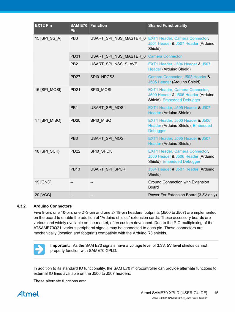
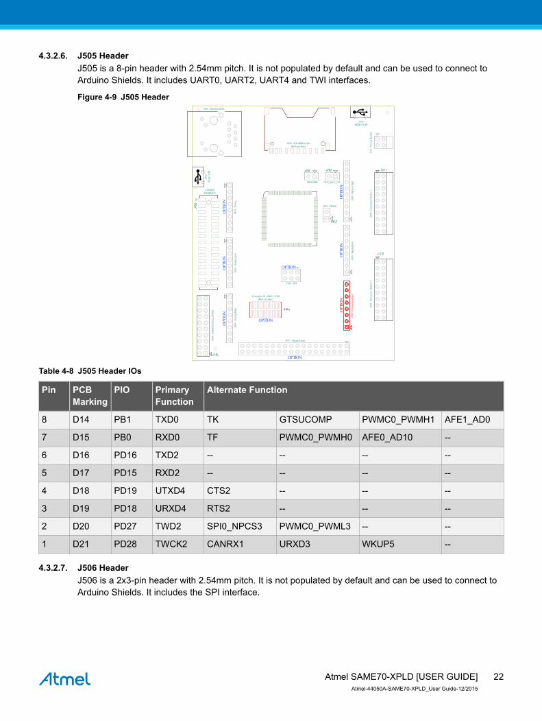
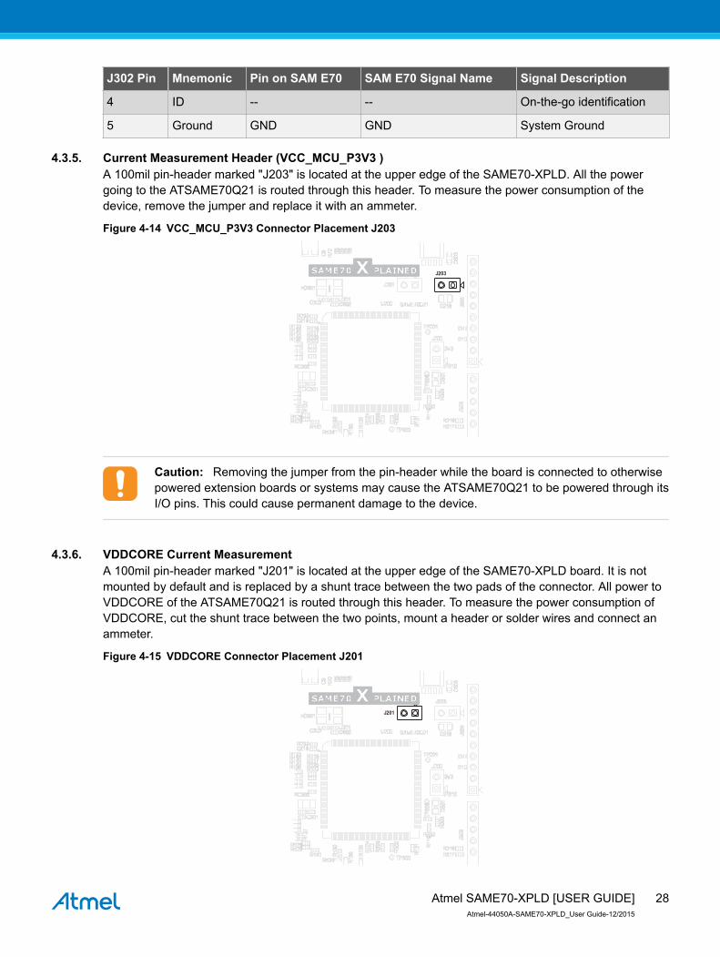
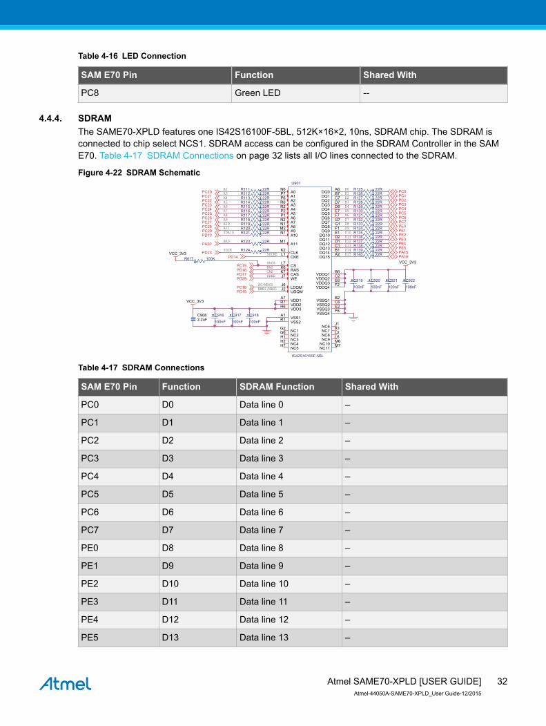
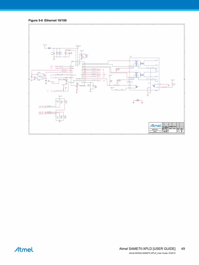


![Atmel ATSHA204 - SparkFun Electronicscdn.sparkfun.com/.../Atmel-8740-CryptoAuth-ATSHA204-Datasheet.pdf · Atmel ATSHA204 [DATASHEET] 5 Atmel–8740E–CryptoAuth–ATSHA204–Datasheet–022013](https://img.pdfslide.net/doc/110x75/5e25fe64d9a5567efa4c5ccc/atmel-atsha204-sparkfun-atmel-atsha204-datasheet-5-atmela8740eacryptoauthaatsha204adatasheeta022013.jpg)


![Atmel | SMART SAMA5D3 Series - Microchip Technologyww1.microchip.com/downloads/en/DeviceDoc/Atmel-11269-32...SAMA5D3 Xplained [USER GUIDE] Atmel-11269D-ATARM-SAMA5D3-Xplained-XPLD-User](https://img.pdfslide.net/doc/110x75/5aedd4107f8b9a3669917d67/atmel-smart-sama5d3-series-microchip-xplained-user-guide-atmel-11269d-atarm-sama5d3-xplained-xpld-user.jpg)