Embed Size (px)
Citation preview

Sample and Hold Circuits p(chapter 8)
Tuesday 2nd of February, 2010uesday d o eb ua y, 0 0
Snorre Aunet, [email protected] Group, Dept. of Informatics
Office 3432

Last time – Tuesday 26th of January• Practical issues• Learning goals• Design project, tools and methods• Syllabus
V b i f i t d ti t i• Very brief introduction to various circuit building blocks
(sample-and-holds bandgap(sample and holds, bandgap references, switched capacitor circuits, nyquist- and oversampling data converters, phase-locked loops)

Sample and Holds (S/H) – What are the purposes?p ( ) p p• Mainly used in Analog-to-Digital Converters (ADC)
• Samples analog input signal and holds value betweenSamples analog input signal and holds value between clock cycles
• Stable input value is required in many ADC-topologiesR d ADC d b i t l ADC d l• Reduces ADC-error caused by internal ADC delay variations
• Sometimes referred to as Track and Hold (T/H)Sometimes referred to as Track and Hold (T/H)• Important parameters for S/H’s
• Hold step: Voltage error during S/H-transitionSi l i l i i h ld d• Signal isolation in hold mode
• Input signal tracking speed in sample mode• Droop rate in hold mode: Small change in output voltageDroop rate in hold mode: Small change in output voltage• Aperture jitter: Sampling time uncertainty

Overview of signal spectra – conceptual and physical realizations
convert todiscrete-time
sequenceDSP
convert toimpulse
trainhold
analoglow-pass
filter
xc t( )
s t( )
xs t( )
x n( ) xc nT( )= y n( ) ys t( ) ysh t( )
yc t( )
sequence train filter
A/Dsample analogD/Axc t( )
xsh t( ) x n( ) xc nT( )= y n( )ysh t( )
y t( )
• An anti-aliasing filter (not shown) is assumed to band limit
DSPA/D
converterlow-pass
filterandhold
converterwith hold
yc t( )
An anti-aliasing filter (not shown) is assumed to band limit the continous time signal, xc(t).
• DSP (”discrete-time signal processing”) may beDSP ( discrete time signal processing ) may be accomplished using fully digital processing or discrete-time analog circuits (ex.: SC-circ.)
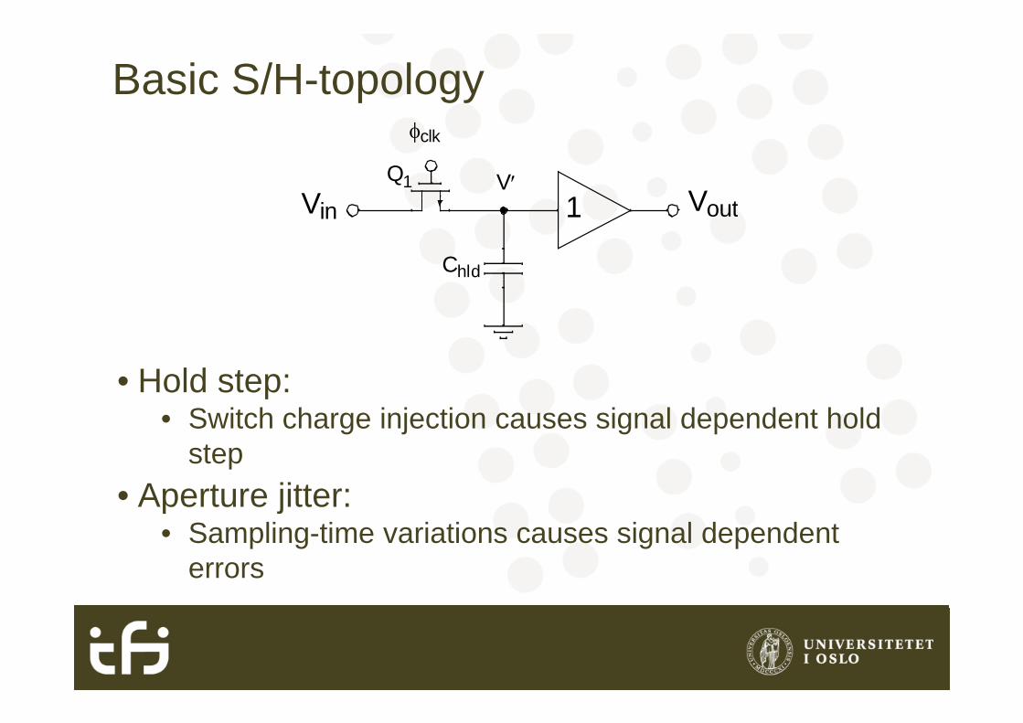
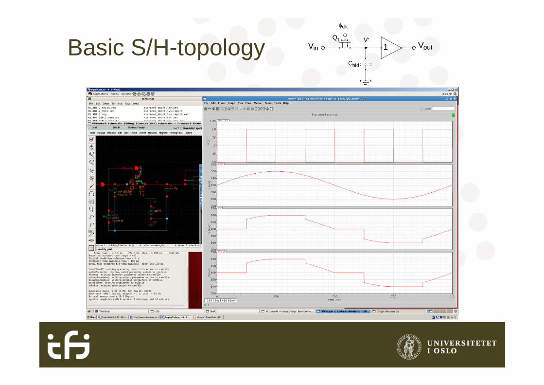
Basic S/H-topology
V V1
clk
Q1 VVin Vout1
Chld
• Hold step:• Switch charge injection causes signal dependent hold
tstep• Aperture jitter:
S li ti i ti i l d d t• Sampling-time variations causes signal dependent errors
Basic S/H-topology Vin Vout1
clk
C
Q1 V
Chld

Charge injection due to channel capacitance clkWhen goes low, the channel charge of is equally distributed between source and
drain, leaving 50% of the charge across Chld:Q1
QChld
QCH2
-----------CoxWLVeff-1
2---------------------------------= =
Veff-1 VGS1 Vtn– VDD Vtn Vin––= =clk
Q
VQC-hld
Chld------------------- CoxWL VDD Vtn Vin––
2Chld----------------------------------------------------------------–= =
Vin Vout1
Chld
Q1 V
• is linearly related to Vin, resulting in a gain error for the S/H. There is also a linear relationship to Vtn which is nonlinearly relatedV
There is also a linear relationship to Vtn, which is nonlinearly related to Vin ( through Vsb ) resulting in distortion for the overall S/H.

Charge injection due to the gate overlap capacitance:
•C WL V VSS–
VCox WLov VDD VSS–
Chld--------------------------------------------------------–
• (See eq. 7.8) This component is usually smaller than that due to the channel charge and appearsthan that due to the channel charge, and appears as an offset, since it’s signal independent. Thus it may be removed in most systemsThus it may be removed in most systems.
• The clock signal should be relatively noise free, as the power-supply rejection of this S/H might be poor (if forpower-supply rejection of this S/H might be poor. (if for example clock signal comes from an inverter with common Vdd and Vss)

Hold step reductionclk
Vin Vout1
Q1 V
clk
Vin Vout1Q1 VQ2
clkclkslightly delayed
Chldclk
Chld
• Transmission gate reduces charge injection since the charge carriers in the NMOS d PMOS h i d l it > Th ti h f th
CMOS transmission gate Dummy switch
NMOS and PMOS have inversed polarity -> The negative charge from the NMOS cancels the positive charge from the PMOS
• PMOS and NMOS are however hard to match in size, reducing the benefitreducing the benefit.
• A NMOS dummy switch (S and D short-circuited) of half channel area clocked on inverted clock may be used to absorb charge
• Hold step reduced by approximately 80%p y pp y %• The dummy switch clock must be slightly delayed to ensure that no charge leaks
through Q1 while it is still open

Aperture jitter
t 1 id l t
ts1-actual Vin clk
Vin Vout1
clk
Q1 V
ts1-ideal ts2-ideal
ts2-actual
Chld
If h i l i l h h iSampling jitter
• If the input voltage is lower than the capacitor voltage, Vin is the source of the transistor used as a
it hswitch• Vgs is then depending on Vin. For high values of Vin,
the switch turns off too fast while for low values of Vin it turns off too late causing distortion

S/H (fig. 8.7)
1Q1
V
clk
• Advantages:
Vin
Chld
1 Vout
buffer
• High input impedance• Buffer offset voltage is divided by the gain of the input opamp,
due to negative feedback Simple voltage follower may be useddue to negative feedback. Simple voltage follower may be used at the output.
• Disadvantages:E d t fi it l k i d f ll ti (PMOS d NMOS• Errors due to finite clock rise- and fall-times (PMOS and NMOS are not switched off at the same time)
• Signal dependent charge injection -> Distortion• Feedback loop and need for stability limit maximum speed• In Hold mode, the first opamp output goes to either rail. Must slew
back

Sample-and-Hold from fig. 8.7

Increased speed (fig. 8.8)clk
Q3
clk
clkQ2
VinVout
C
1Q1
D i h ld d h i ki h
Chld
• During hold mode the opamp output is tracking the input
L d t i d d• Leads to increased speed• Disadvantages in common with the previous circuit

SAMPLE (= Track) / HOLD modes (fig 8.8)
3. februar 2010 14

Sample-and-Hold from fig. 8.8

Another S/H: Fig 8.9 (Improved version of the S/H from fig 8 8 )fig. 8.8 )
3. februar 2010 16

Sample (track) mode to Hold mode (the S/H in fig. 8.9) signals, from top: Voutopamp1, V(Q2) V(Q1), Vout , Vin) g , p outopamp1, (Q2), (Q1), out , in
3. februar 2010 17

S/H with hold step independent of input signal (fig 8-9)(fig. 8-9)
ChldclkOpamp 1
Vin Vout
Q1
clk Q2
+ : Both sides of Q1 are nearly signal independent so that the
clk Q2 Opamp 2
+ : Both sides of Q1 are nearly signal independent, so that the charge injection is (nearly) signal independent, provided a sufficient gain in the 2nd Opamp. The charge injection on Chldcauses the output of the 2nd Opamp to have a positive holdcauses the output of the 2nd Opamp to have a positive hold step, which is just a dc offset, with no signal distortion, and signal independent.S li ti ill t h d t fi it l f th+: Sampling time will not change due to finite slopes of the sampling clock less aperture jitter / aperture uncertainty sample value closer to the ideal one.

S/H with hold step independent of input signal (fig 8-9)(fig. 8-9)
ChldclkOpamp 1
Vin Vout
Q1
clk Q2
+ : Q2 ground the output of OPAMP1 in hold mode, meaning that it’s
clk Q2 Opamp 2
close to (and quickly getting to) the voltage it should have in S. mode, which improves speed.
- Preventing instability reduces speed• Worsened due to two opamps in the feedback loop
• More relevant information: K. R. Stafford, P. R. Gray, R. A. yBlanchard: ”A Complete Monolithic Sample/Hold Amplifier”, IEEE Journal of Solid-State Circuits, Dec. 1974. ( available from http://ieeexplore.ieee.org , when on UiO IP-address )

”New(er) architecture”
3. februar 2010 20

Continous efforts to improve S/H circuits..
IEEEX l id S f h A• IEEEXplore may provide State-of-the-Art solutions3. februar 2010 21

Reduced DC-error (fig. 8-10)Chld
clk
Vin Vout
Q1
lkclk Q3 clkQ2
Chld
• Improved version of previous circuit (in fig. 8.9)B l i f Q1 d Chld i ll l b d d h i i• By placing a copy of Q1 and Chld in parallel between ground and the positive input of the second opamp, the voltage change due to charge injection will be equal on both inputs. Error is cancelled by opamp CMRR. Th d j ti ti (CMRR) f diff ti l lifi ( thThe common-mode rejection ratio (CMRR) of a differential amplifier (or other device) measures the tendency of the device to reject input signals common to both input leads.

Additional Background Litterature, S/H circuitsg ,• A. S. Sedra, K. C. Smith: ”Microelectronic Circuits”, Saunders College
Publishing, 1991.g,• R. Gregorian, G. C. Temes: ”Analog MOS Integrated Circuits for signal
processing”, Wiley, 1986.• K. R. Stafford, P. R. Gray, R. A. Blanchard: ”A Complete Monolithic Sample/HoldK. R. Stafford, P. R. Gray, R. A. Blanchard: A Complete Monolithic Sample/Hold
Amplifier”, IEEE Journal of Solid-State Circuits, Dec. 1974.• F. F. Kuo:”Network Analysis and Synthesis”, Wiley, 1966.• S Soma: ”Grunnbok i elektronikk” Universitetsforlaget 1979• S. Soma: Grunnbok i elektronikk , Universitetsforlaget, 1979.• National Semiconductor: ”Specifcations and Architectures of Sample-and-Hold
Architectures”, App. Note 775, July 1992.• S Aunet: ”BiCMOS Sample and Hold for Satelittkommunikasjon”• S. Aunet: BiCMOS Sample-and-Hold for Satelittkommunikasjon ,
hovedfagsoppgave, UiO, 1993.
3. februar 2010 23

S/H stuff..
3. februar 2010 24
![ANALYSIS OF SAMPLE AND HOLD CIRCUITS FOR ANALOG TO …kphang/papers/2002/... · note that most sample and hold circuits actually perform a track and hold function [3], however I shall](https://img.pdfslide.net/doc/110x75/5f3210293bb6e26dfe534132/analysis-of-sample-and-hold-circuits-for-analog-to-kphangpapers2002-note.jpg)