Embed Size (px)
Citation preview
- 1 -
SAMSUNG ELECTRONICS RESERVES THE RIGHT TO CHANGE PRODUCTS, INFORMATION AND SPECIFICATIONS WITHOUT NOTICE.
Products and specifications discussed herein are for reference purposes only. All information discussed herein is provided on an "AS IS" basis, without warranties of any kind.
This document and all information discussed herein remain the sole and exclusive property of Samsung Electronics. No license of any patent, copyright, mask work, trademark or any other intellectual property right is granted by one party to the other party under this document, by implication, estoppel or other-wise.
Samsung products are not intended for use in life support, critical care, medical, safety equipment, or similar applications where product failure could result in loss of life or personal or physical harm, or any military or defense application, or any governmental procurement to which special terms or provisions may apply.
For updates or additional information about Samsung products, contact your nearest Samsung office.
All brand names, trademarks and registered trademarks belong to their respective owners.
2011 Samsung Electronics Co., Ltd. All rights reserved.
Rev. 1.0, Oct. 2011
KLMxGxFE3B-x00x
Samsung e·MMC Product familye.MMC 4.41 Specification compatibility
datasheet
- 2 -
datasheet e·MMCRev. 1.0
KLMxGxFE3B-x00x
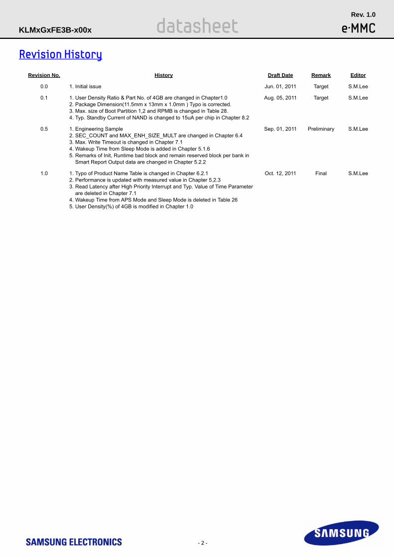
Revision History
Revision No. History Draft Date Remark Editor
0.0 1. Initial issue Jun. 01, 2011 Target S.M.Lee
0.1 1. User Density Ratio & Part No. of 4GB are changed in Chapter1.02. Package Dimension(11.5mm x 13mm x 1.0mm ) Typo is corrected.3. Max. size of Boot Partition 1,2 and RPMB is changed in Table 28.4. Typ. Standby Current of NAND is changed to 15uA per chip in Chapter 8.2
Aug. 05, 2011 Target S.M.Lee
0.5 1. Engineering Sample2. SEC_COUNT and MAX_ENH_SIZE_MULT are changed in Chapter 6.43. Max. Write Timeout is changed in Chapter 7.14. Wakeup Time from Sleep Mode is added in Chapter 5.1.65. Remarks of Init, Runtime bad block and remain reserved block per bank in Smart Report Output data are changed in Chapter 5.2.2
Sep. 01, 2011 Preliminary S.M.Lee
1.0 1. Typo of Product Name Table is changed in Chapter 6.2.12. Performance is updated with measured value in Chapter 5.2.33. Read Latency after High Priority Interrupt and Typ. Value of Time Parameter are deleted in Chapter 7.14. Wakeup Time from APS Mode and Sleep Mode is deleted in Table 26 5. User Density(%) of 4GB is modified in Chapter 1.0
Oct. 12, 2011 Final S.M.Lee
- 3 -
datasheet e·MMCRev. 1.0
KLMxGxFE3B-x00x
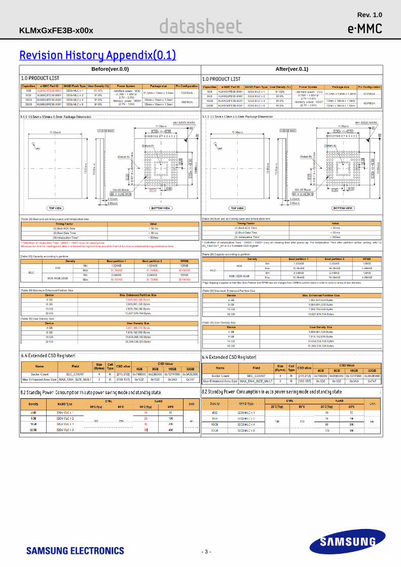
Revision History Appendix(0.1)Before(ver.0.0) After(ver.0.1)
- 4 -
datasheet e·MMCRev. 1.0
KLMxGxFE3B-x00x
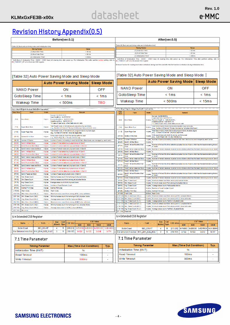
Revision History Appendix(0.5)Before(ver.0.1) After(ver.0.5)
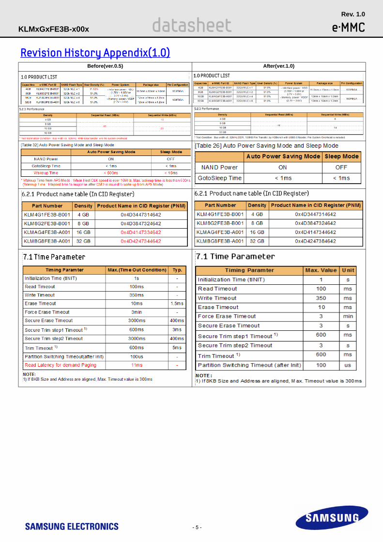
- 5 -
datasheet e·MMCRev. 1.0
KLMxGxFE3B-x00x
Revision History Appendix(1.0)Before(ver.0.5) After(ver.1.0)
Table Of Contents
- 6 -
datasheet e·MMCRev. 1.0
KLMxGxFE3B-x00x
1.0 PRODUCT LIST..........................................................................................................................................................6
2.0 KEY FEATURES......................................................................................................................................................... 6
3.0 PACKAGE CONFIGURATIONS ................................................................................................................................. 73.1 153 Ball Pin Configuration ....................................................................................................................................... 7
3.1.1 11.5mm x 13mm x 1.0mm Package Dimension................................................................................................ 83.2 169 Ball Pin Configuration ....................................................................................................................................... 9
3.2.1 12mm x 16mm x 1.0mm Package Dimension................................................................................................... 103.2.2 12mm x 16mm x 1.2mm Package Dimension................................................................................................... 11
3.3 Product Architecture ................................................................................................................................................ 12
4.0 e.MMC 4.41 features .................................................................................................................................................. 134.1 Data Write................................................................................................................................................................ 134.2 Reliable Write .......................................................................................................................................................... 144.3 Secure Trim ............................................................................................................................................................. 144.4 High Priority Interrupt............................................................................................................................................... 144.5 Background Operation............................................................................................................................................. 16
5.0 Technical Notes ..........................................................................................................................................................175.1 S/W Agorithm .......................................................................................................................................................... 17
5.1.1 Partition Management ....................................................................................................................................... 175.1.1.1 Boot Area Partition and RPMB Area Partition ............................................................................................ 175.1.1.2 Enhanced Partition (Area) .......................................................................................................................... 17
5.1.2 Write protect management................................................................................................................................ 185.1.2.1 User Area Write Protection ......................................................................................................................... 185.1.2.2 Boot Partition Write Protection.................................................................................................................... 18
5.1.3 Boot operation................................................................................................................................................... 195.1.4 Wear Leveling ................................................................................................................................................... 205.1.5 User Density...................................................................................................................................................... 205.1.6 Auto Power Saving Mode.................................................................................................................................. 215.1.7 End of Life Management ................................................................................................................................... 21
5.2 Smart Report ........................................................................................................................................................... 225.2.1 Smart Report Sequence.................................................................................................................................... 225.2.2 Smart Report Output Data (For Customer) ....................................................................................................... 235.2.3 Performance ..................................................................................................................................................... 23
6.0 REGISTER VALUE..................................................................................................................................................... 246.1 OCR Register .......................................................................................................................................................... 246.2 CID Register ............................................................................................................................................................ 24
6.2.1 Product name table (In CID Register) ............................................................................................................... 246.3 CSD Register........................................................................................................................................................... 256.4 Extended CSD Register .......................................................................................................................................... 26
7.0 AC PARAMETER........................................................................................................................................................ 297.1 Time Parameter....................................................................................................................................................... 297.2 Bus Timing Parameter............................................................................................................................................. 297.3 Bus timing for DAT signals during 2x data rate operation ....................................................................................... 31
7.3.1 Dual data rate interface timings ........................................................................................................................ 317.4 Bus signal levels...................................................................................................................................................... 32
7.4.1 Open-drain mode bus signal level..................................................................................................................... 327.4.2 Push-pull mode bus signal level.high-voltage MultiMediaCard......................................................................... 327.4.3 Push-pull mode bus signal level.dual-voltage MultiMediaCard......................................................................... 327.4.4 Push-pull mode bus signal level.e·MMC........................................................................................................... 33
8.0 DC PARAMETER .......................................................................................................................................................348.1 Active Power Consumption during operation ......................................................................................................... 348.2 Standby Power Consumption in auto power saving mode and standby state........................................................ 348.3 Sleep Power Consumption in Sleep State.............................................................................................................. 348.4 Supply Voltage ........................................................................................................................................................ 348.5 Bus Operating Conditions........................................................................................................................................ 348.6 Bus Signal Line Load............................................................................................................................................... 35
9.0 e·MMC Connection Guide .......................................................................................................................................... 369.1 x8 support Host connection Guide .......................................................................................................................... 369.2 x4 support Host connection Guide .......................................................................................................................... 36
- 6 -
datasheet e·MMCRev. 1.0
KLMxGxFE3B-x00x
INTRODUCTION
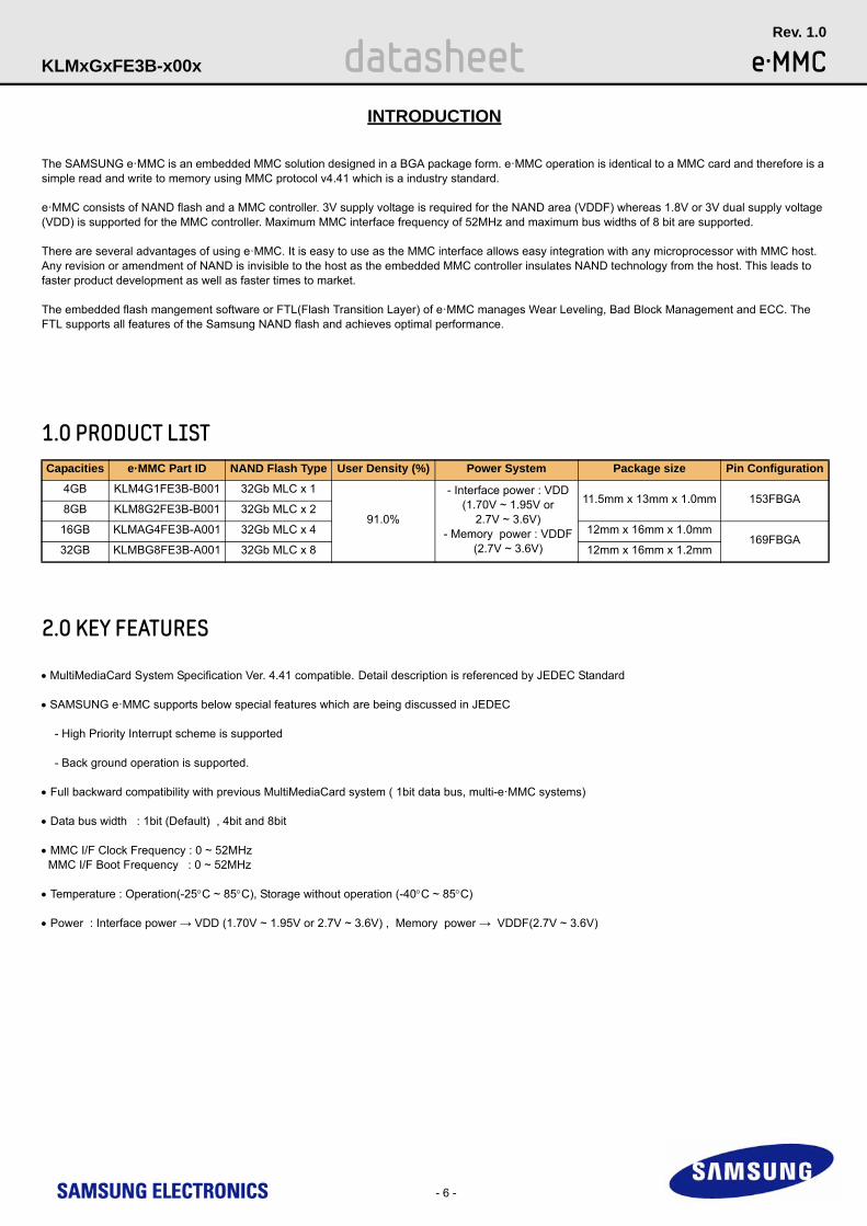
The SAMSUNG e·MMC is an embedded MMC solution designed in a BGA package form. e·MMC operation is identical to a MMC card and therefore is a simple read and write to memory using MMC protocol v4.41 which is a industry standard.
e·MMC consists of NAND flash and a MMC controller. 3V supply voltage is required for the NAND area (VDDF) whereas 1.8V or 3V dual supply voltage (VDD) is supported for the MMC controller. Maximum MMC interface frequency of 52MHz and maximum bus widths of 8 bit are supported.
There are several advantages of using e·MMC. It is easy to use as the MMC interface allows easy integration with any microprocessor with MMC host. Any revision or amendment of NAND is invisible to the host as the embedded MMC controller insulates NAND technology from the host. This leads to faster product development as well as faster times to market.
The embedded flash mangement software or FTL(Flash Transition Layer) of e·MMC manages Wear Leveling, Bad Block Management and ECC. The FTL supports all features of the Samsung NAND flash and achieves optimal performance.
1.0 PRODUCT LIST
- Interface power : VDD (1.70V ~ 1.95V or
2.7V ~ 3.6V) - Memory power : VDDF
(2.7V ~ 3.6V)
11.5mm x 13mm x 1.0mm
12mm x 16mm x 1.0mm
12mm x 16mm x 1.2mm
2.0 KEY FEATURES
MultiMediaCard System Specification Ver. 4.41 compatible. Detail description is referenced by JEDEC Standard
SAMSUNG e·MMC supports below special features which are being discussed in JEDEC
- High Priority Interrupt scheme is supported
- Back ground operation is supported.
Full backward compatibility with previous MultiMediaCard system ( 1bit data bus, multi-e·MMC systems)
Data bus width : 1bit (Default) , 4bit and 8bit
MMC I/F Clock Frequency : 0 ~ 52MHz MMC I/F Boot Frequency : 0 ~ 52MHz
Temperature : Operation(-25C ~ 85C), Storage without operation (-40C ~ 85C)
Power : Interface power → VDD (1.70V ~ 1.95V or 2.7V ~ 3.6V) , Memory power → VDDF(2.7V ~ 3.6V)
Capacities e·MMC Part ID NAND Flash Type User Density (%) Power System Package size Pin Configuration
4GB KLM4G1FE3B-B001 32Gb MLC x 1
91.0%
153FBGA8GB KLM8G2FE3B-B001 32Gb MLC x 2
16GB KLMAG4FE3B-A001 32Gb MLC x 4169FBGA
32GB KLMBG8FE3B-A001 32Gb MLC x 8
- 7 -
datasheet e·MMCRev. 1.0
KLMxGxFE3B-x00x
3.0 PACKAGE CONFIGURATIONS
Figure 1. 153-FBGA
3.1 153 Ball Pin Configuration
[Table 1] 153 Ball Information
Pin NO Name
A3 DAT0
A4 DAT1
A5 DAT2
B2 DAT3
B3 DAT4
B4 DAT5
B5 DAT6
B6 DAT7
K5 RSTN
C6 VDD
M4 VDD
N4 VDD
P3 VDD
P5 VDD
E6 VDDF
F5 VDDF
J10 VDDF
K9 VDDF
C2 VDDI
M5 CMD
M6 CLK
C4 VSS
E7 VSS
G5 VSS
H10 VSS
K8 VSS
N2 VSS
N5 VSS
P4 VSS
P6 VSS
Vss
VDDF
VDDFVss
Vss
DAT7
VDD
VDDF
CLK
Vss
DAT2
DAT6
VDDF
Vss
RSTN
CMD
Vss
VDD
DAT1
DAT5
Vss
VDD
VDD
Vss
DAT4
VDD
DAT3
Vss
DAT0
VDDI
DNU
DNU
DNUDNU
DNU
NC
DNU
DNU
DNU
DNU
DNU
DNU
DNUDNU
DNU
DNU DNU
DNU
DNU
DNU
DNU
DNU DNU
DNU
DNU
DNU
DNU DNU
DNUDNU
DNU
DNU
DNU
DNU
DNU
DNU
A
B
C
D
E
F
G
H
J
K
L
M
N
P
1 2 3 4 5 6 7 8 9 10 11 12 13 14
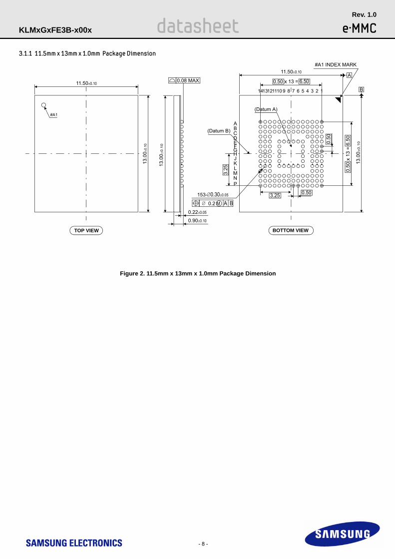
Figure 2. 11.5mm x 13mm x 1.0mm Package Dimension
- 8 -
datasheet e·MMCRev. 1.0
KLMxGxFE3B-x00x
3.1.1 11.5mm x 13mm x 1.0mm Package Dimension
0.08 MAX
0.90±0.10
TOP VIEW
11.50±0.10
#A1
13.0
0±0
.10
#A1 INDEX MARK
BOTTOM VIEW
0.22±0.05
14 14 27 6 5 389111312 10
0.50 x 13 = 6.50
11.50±0.10A
B
(Datum A)
0.50
13.0
0±0
.10
0.50
(Datum B)
153-0.30±0.05
0.2 M A B
3.25
ABC
ED
F
HJ
LK
NP
G
M
13.
00±0
.10
3.25
0.50
x 1
3 =
6.5
0
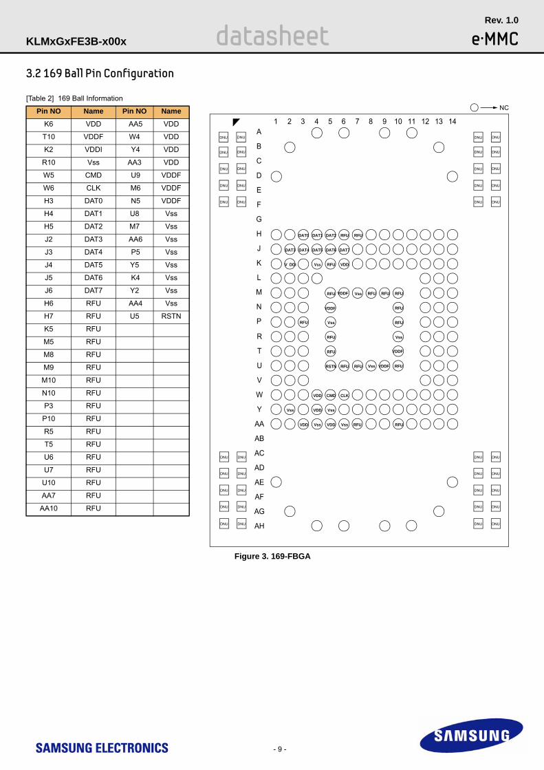
Figure 3. 169-FBGA
- 9 -
datasheet e·MMCRev. 1.0
KLMxGxFE3B-x00x
3.2 169 Ball Pin Configuration
[Table 2] 169 Ball Information
Pin NO Name Pin NO Name
K6 VDD AA5 VDD
T10 VDDF W4 VDD
K2 VDDI Y4 VDD
R10 Vss AA3 VDD
W5 CMD U9 VDDF
W6 CLK M6 VDDF
H3 DAT0 N5 VDDF
H4 DAT1 U8 Vss
H5 DAT2 M7 Vss
J2 DAT3 AA6 Vss
J3 DAT4 P5 Vss
J4 DAT5 Y5 Vss
J5 DAT6 K4 Vss
J6 DAT7 Y2 Vss
H6 RFU AA4 Vss
H7 RFU U5 RSTN
K5 RFU
M5 RFU
M8 RFU
M9 RFU
M10 RFU
N10 RFU
P3 RFU
P10 RFU
R5 RFU
T5 RFU
U6 RFU
U7 RFU
U10 RFU
AA7 RFU
AA10 RFU
DNU
DNU
DNUDNU
DNU
DNU
RFU
RFU
RFU
Vss
VDDF
RFU
RFU
VDDF
RFU
Vss
RFU
Vss
RFU
RFU
DAT7
VDD
VDDF
RFU
CLK
Vss
DAT2
DAT6
RFU
RFU
VDDF
Vss
RFU
RFU
RSTN
CMD
Vss
VDD
DAT1
DAT5
Vss
VDD
VDD
Vss
DAT4
VDD
DAT3
Vss
A
B
C
D
E
F
G
H
J
K
L
M
N
P
DAT0
1 2 3 4 5 6 7 8 9 10 11 12 13 14
V DDI
R
T
U
V
W
Y
AA
AB
AC
AD
AE
AF
AG
AH
DNU
DNU
DNUDNU
DNUDNU
DNU
DNU
DNU
DNUDNU
DNUDNU
DNU
DNU
RFU RFU
RFU
DNU
DNUDNU
DNUDNU
DNU DNU
DNU
DNU
DNUDNU
DNU
DNU
DNUDNU
DNU DNU
DNUDNU
NC

Figure 4. 12mm x 16mm x 1.0mm Package Dimension
- 10 -
datasheet e·MMCRev. 1.0
KLMxGxFE3B-x00x
3.2.1 12mm x 16mm x 1.0mm Package Dimension
0.08 MAX
0.90±0.10
TOP VIEW
12.00±0.10
16.
00±0.1
0
#A1
16
.00
±0.1
0
#A1 INDEX MARK
BOTTOM VIEW
0.22±0.05
14 14 27 6 5 389111312 10
0.50 x 13 = 6.50
12.00±0.10A
B(Datum A)
0.5
0
0.2
5
0.5
0 x
13
= 6
.50
16
.00
±0.1
0
0.50
(Datum B)
169-0.30±0.05
0.2 M A B
1.75
0.25
0.75
2.75
3.25
5.2
5
6.2
5
6.7
5
ABC
ED
F
HJ
LK
NP
G
M
RTU
WV
Y
ABAC
AEAD
AGAH
AA
AF
SIDE VIEW
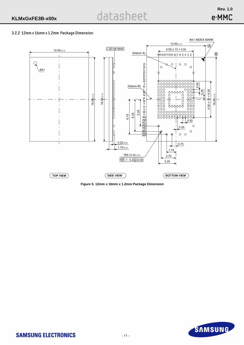
Figure 5. 12mm x 16mm x 1.2mm Package Dimension
- 11 -
datasheet e·MMCRev. 1.0
KLMxGxFE3B-x00x
3.2.2 12mm x 16mm x 1.2mm Package Dimension
0.08 MAX
1.10±0.10
TOP VIEW
12.00±0.10
16.
00±0.1
0
#A1
16
.00
±0.1
0
#A1 INDEX MARK
BOTTOM VIEW
0.22±0.05
14 14 27 6 5 389111312 10
0.50 x 13 = 6.50
12.00±0.10A
B(Datum A)
0.5
0
0.2
5
0.5
0 x
13
= 6
.50
16
.00
±0.1
0
0.50
(Datum B)
169-0.30±0.05
0.2 M A B
1.75
0.25
0.75
2.75
3.25
5.2
5
6.2
5
6.7
5
ABC
ED
F
HJ
LK
NP
G
M
RTU
WV
Y
ABAC
AEAD
AGAH
AA
AF
SIDE VIEW
- 12 -
datasheet e·MMCRev. 1.0
KLMxGxFE3B-x00x
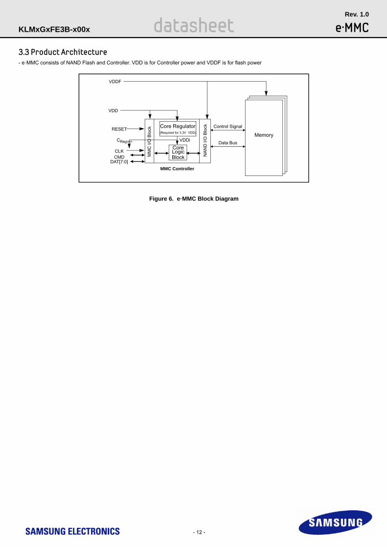
3.3 Product Architecture
Figure 6. e·MMC Block Diagram
Control Signal
Data Bus
MMC Controller
VDDF
Core Regulator
Core
Memory
NA
ND
I/O
Blo
ck
MM
C I
/O B
lock
LogicBlock
(Required for 3.3V VDD)
VDD
RESET
VDDi
CLKCMD
DAT[7:0]
CReg
- e·MMC consists of NAND Flash and Controller. VDD is for Controller power and VDDF is for flash power
- 13 -
datasheet e·MMCRev. 1.0
KLMxGxFE3B-x00x
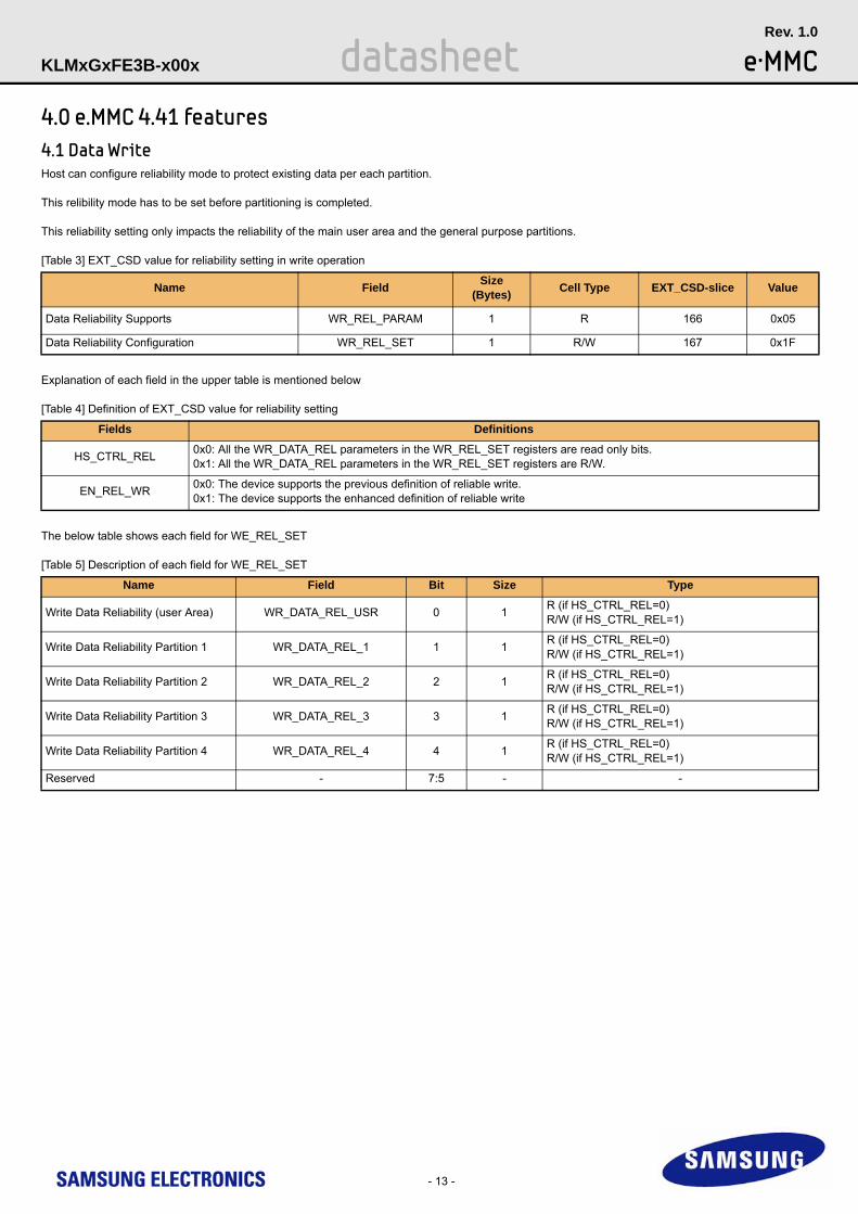
4.0 e.MMC 4.41 features4.1 Data WriteHost can configure reliability mode to protect existing data per each partition.
This relibility mode has to be set before partitioning is completed.
This reliability setting only impacts the reliability of the main user area and the general purpose partitions.
[Table 3] EXT_CSD value for reliability setting in write operation
Explanation of each field in the upper table is mentioned below
[Table 4] Definition of EXT_CSD value for reliability setting
The below table shows each field for WE_REL_SET
[Table 5] Description of each field for WE_REL_SET
Name FieldSize
(Bytes)Cell Type EXT_CSD-slice Value
Data Reliability Supports WR_REL_PARAM 1 R 166 0x05
Data Reliability Configuration WR_REL_SET 1 R/W 167 0x1F
Fields Definitions
HS_CTRL_REL0x0: All the WR_DATA_REL parameters in the WR_REL_SET registers are read only bits.0x1: All the WR_DATA_REL parameters in the WR_REL_SET registers are R/W.
EN_REL_WR0x0: The device supports the previous definition of reliable write.0x1: The device supports the enhanced definition of reliable write
Name Field Bit Size Type
Write Data Reliability (user Area) WR_DATA_REL_USR 0 1R (if HS_CTRL_REL=0)R/W (if HS_CTRL_REL=1)
Write Data Reliability Partition 1 WR_DATA_REL_1 1 1R (if HS_CTRL_REL=0)R/W (if HS_CTRL_REL=1)
Write Data Reliability Partition 2 WR_DATA_REL_2 2 1R (if HS_CTRL_REL=0)R/W (if HS_CTRL_REL=1)
Write Data Reliability Partition 3 WR_DATA_REL_3 3 1R (if HS_CTRL_REL=0)R/W (if HS_CTRL_REL=1)
Write Data Reliability Partition 4 WR_DATA_REL_4 4 1R (if HS_CTRL_REL=0)R/W (if HS_CTRL_REL=1)
Reserved - 7:5 - -
- 14 -
datasheet e·MMCRev. 1.0
KLMxGxFE3B-x00x
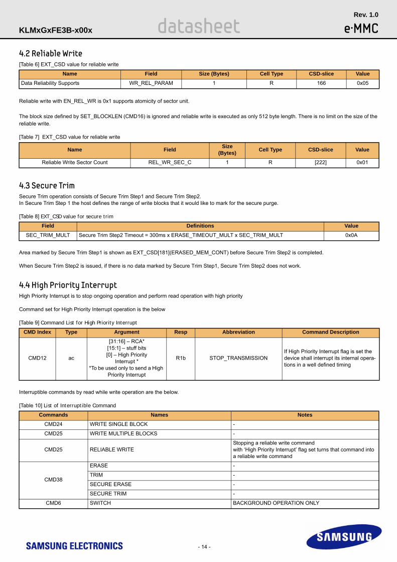
4.2 Reliable Write[Table 6] EXT_CSD value for reliable write
Reliable write with EN_REL_WR is 0x1 supports atomicity of sector unit.
The block size defined by SET_BLOCKLEN (CMD16) is ignored and reliable write is executed as only 512 byte length. There is no limit on the size of the reliable write.
[Table 7] EXT_CSD value for reliable write
4.3 Secure TrimSecure Trim operation consists of Secure Trim Step1 and Secure Trim Step2.In Secure Trim Step 1 the host defines the range of write blocks that it would like to mark for the secure purge.
[Table 8] EXT_CSD value for secure trim
Area marked by Secure Trim Step1 is shown as EXT_CSD[181](ERASED_MEM_CONT) before Secure Trim Step2 is completed.
When Secure Trim Step2 is issued, if there is no data marked by Secure Trim Step1, Secure Trim Step2 does not work.
4.4 High Priority InterruptHigh Priority Interrupt is to stop ongoing operation and perform read operation with high priority
Command set for High Priority Interrupt operation is the below
[Table 9] Command List for High Priority Interrupt
Interruptible commands by read while write operation are the below.
[Table 10] List of Interruptible Command
Name Field Size (Bytes) Cell Type CSD-slice Value
Data Reliability Supports WR_REL_PARAM 1 R 166 0x05
Name FieldSize
(Bytes)Cell Type CSD-slice Value
Reliable Write Sector Count REL_WR_SEC_C 1 R [222] 0x01
Field Definitions Value
SEC_TRIM_MULT Secure Trim Step2 Timeout = 300ms x ERASE_TIMEOUT_MULT x SEC_TRIM_MULT 0x0A
CMD Index Type Argument Resp Abbreviation Command Description
CMD12 ac
[31:16] – RCA*[15:1] – stuff bits[0] – High Priority
Interrupt **To be used only to send a High
Priority Interrupt
R1b STOP_TRANSMISSIONIf High Priority Interrupt flag is set the device shall interrupt its internal opera-tions in a well defined timing
Commands Names Notes
CMD24 WRITE SINGLE BLOCK -
CMD25 WRITE MULTIPLE BLOCKS -
CMD25 RELIABLE WRITEStopping a reliable write commandwith ‘High Priority Interrupt’ flag set turns that command into a reliable write command
CMD38
ERASE -
TRIM -
SECURE ERASE -
SECURE TRIM -
CMD6 SWITCH BACKGROUND OPERATION ONLY
- 15 -
datasheet e·MMCRev. 1.0
KLMxGxFE3B-x00x
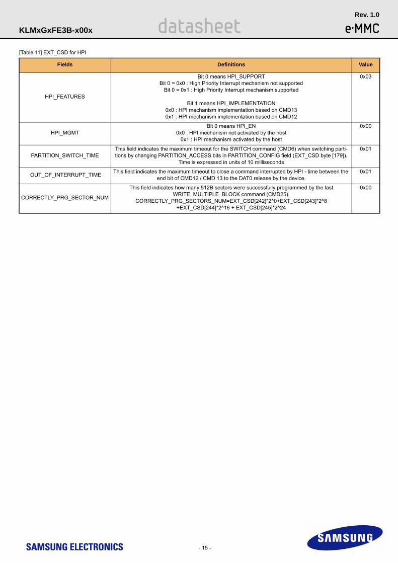
[Table 11] EXT_CSD for HPI
Fields Definitions Value
HPI_FEATURES
Bit 0 means HPI_SUPPORTBit 0 = 0x0 : High Priority Interrupt mechanism not supported
Bit 0 = 0x1 : High Priority Interrupt mechanism supported
Bit 1 means HPI_IMPLEMENTATION0x0 : HPI mechanism implementation based on CMD130x1 : HPI mechanism implementation based on CMD12
0x03
HPI_MGMTBit 0 means HPI_EN
0x0 : HPI mechanism not activated by the host0x1 : HPI mechanism activated by the host
0x00
PARTITION_SWITCH_TIMEThis field indicates the maximum timeout for the SWITCH command (CMD6) when switching parti-tions by changing PARTITION_ACCESS bits in PARTITION_CONFIG field (EXT_CSD byte [179]).
Time is expressed in units of 10 milliseconds
0x01
OUT_OF_INTERRUPT_TIMEThis field indicates the maximum timeout to close a command interrupted by HPI - time between the
end bit of CMD12 / CMD 13 to the DAT0 release by the device. 0x01
CORRECTLY_PRG_SECTOR_NUM
This field indicates how many 512B sectors were successfully programmed by the last WRITE_MULTIPLE_BLOCK command (CMD25).
CORRECTLY_PRG_SECTORS_NUM=EXT_CSD[242]*2^0+EXT_CSD[243]*2^8+EXT_CSD[244]*2^16 + EXT_CSD[245]*2^24
0x00
- 16 -
datasheet e·MMCRev. 1.0
KLMxGxFE3B-x00x
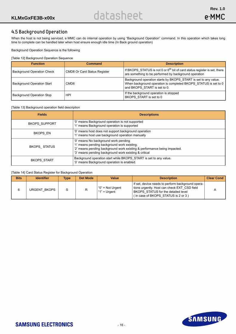
4.5 Background OperationWhen the host is not being serviced, e·MMC can do internal operation by using “Background Operation” command. In this operation which takes long time to complete can be handled later when host ensure enough idle time (In Back ground operation)
Background Operation Sequence is the following
[Table 12] Background Operation Sequence
[Table 13] Background operation field description
[Table 14] Card Status Register for Background Operation
Function Command Description
Background Operation Check CMD8 Or Card Status Register If BKOPS_STATUS is not 0 or 6th bit of card status register is set, there are something to be performed by background operation
Background Operation Start CMD6Background operation starts by BKOPS_START is set to any value.When background operation is completed BKOPS_STATUS is set to 0 and BKOPS_START is set to 0.
Background Operation Stop HPIIf the background operation is stoppedBKOPS_START is set to 0
Fields Descriptions
BKOPS_SUPPORT‘0’ means Background operation is not supported‘1’ means Background operation is supported
BKOPS_EN‘0’ means host does not support background operation‘1’ means host use background operation manually
BKOPS_ STATUS
‘0’ means No background work pending‘1’ means pending background work existing.‘2’ means pending background work existing & performance being impacted.‘3’ means pending background work existing & critical
BKOPS_STARTBackground operation start while BKOPS_START is set to any value.‘0’ means Background operation is enabled.
Bits Identifier Type Det Mode Value Description Clear Cond
6 URGENT_BKOPS S R“0” = Not Urgent“1” = Urgent
If set, device needs to perform background opera-tions urgently. Host can check EXT_CSD field BKOPS_STATUS for the detailed level( in case of BKOPS_STATUS is 2 or 3 )
A
- 17 -
datasheet e·MMCRev. 1.0
KLMxGxFE3B-x00x
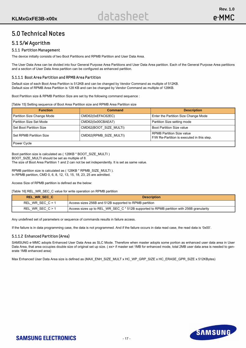
5.0 Technical Notes5.1 S/W Agorithm5.1.1 Partition Management The device initially consists of two Boot Partitions and RPMB Partition and User Data Area.
The User Data Area can be divided into four General Purpose Area Partitions and User Data Area partition. Each of the General Purpose Area partitions and a section of User Data Area partition can be configured as enhanced partition.
5.1.1.1 Boot Area Partition and RPMB Area PartitionDefault size of each Boot Area Partition is 512KB and can be changed by Vendor Command as multiple of 512KB. Default size of RPMB Area Partition is 128 KB and can be changed by Vendor Command as multiple of 128KB.
Boot Partition size & RPMB Partition Size are set by the following command sequence :
[Table 15] Setting sequence of Boot Area Partition size and RPMB Area Partition size
Boot partition size is calculated as ( 128KB * BOOT_SIZE_MULTI )BOOT_SIZE_MULTI should be set as multiple of 8.The size of Boot Area Partition 1 and 2 can not be set independently. It is set as same value.
RPMB partition size is calculated as ( 128KB * RPMB_SIZE_MULTI ).In RPMB partition, CMD 0, 6, 8, 12, 13, 15, 18, 23, 25 are admitted.
Access Size of RPMB partition is defined as the below:
[Table 16] REL_WR_SEC_C value for write operation on RPMB partition
Any undefined set of parameters or sequence of commands results in failure access.
If the failure is in data programming case, the data is not programmed. And if the failure occurs in data read case, the read data is ‘0x00’.
5.1.1.2 Enhanced Partition (Area) SAMSUNG e·MMC adopts Enhanced User Data Area as SLC Mode. Therefore when master adopts some portion as enhanced user data area in User Data Area, that area occupies double size of original set up size. ( ex> if master set 1MB for enhanced mode, total 2MB user data area is needed to gen-erate 1MB enhanced area)
Max Enhanced User Data Area size is defined as (MAX_ENH_SIZE_MULT x HC_WP_GRP_SIZE x HC_ERASE_GPR_SIZE x 512KBytes)
Function Command Description
Partition Size Change Mode CMD62(0xEFAC62EC) Enter the Partition Size Change Mode
Partition Size Set Mode CMD62(0x00CBAEA7) Partition Size setting mode
Set Boot Partition Size CMD62(BOOT_SIZE_MULTI) Boot Partition Size value
Set RPMB Partition Size CMD62(RPMB_SIZE_MULTI)RPMB Partition Size valueF/W Re-Partition is executed in this step.
Power Cycle
REL_WR_SEC_C Description
REL_WR_SEC_C = 1 Access sizes 256B and 512B supported to RPMB partition
REL_WR_SEC_C > 1 Access sizes up to REL_WR_SEC_C * 512B supported to RPMB partition with 256B granularity
- 18 -
datasheet e·MMCRev. 1.0
KLMxGxFE3B-x00x
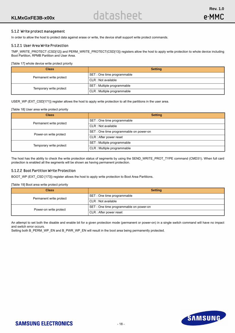
5.1.2 Write protect management In order to allow the host to protect data against erase or write, the device shall support write protect commands.
5.1.2.1 User Area Write Protection TMP_WRITE_PROTECT (CSD[12]) and PERM_WRITE_PROTECT(CSD[13]) registers allow the host to apply write protection to whole device including Boot Partition, RPMB Partition and User Area.
[Table 17] whole device write protect priority
USER_WP (EXT_CSD[171]) register allows the host to apply write protection to all the partitions in the user area.
[Table 18] User area write protect priority
The host has the ability to check the write protection status of segments by using the SEND_WRITE_PROT_TYPE command (CMD31). When full card protection is enabled all the segments will be shown as having permanent protection.
5.1.2.2 Boot Partition Write Protection BOOT_WP (EXT_CSD [173]) register allows the host to apply write protection to Boot Area Partitions.
[Table 19] Boot area write protect priority
An attempt to set both the disable and enable bit for a given protection mode (permanent or power-on) in a single switch command will have no impact and switch error occurs.Setting both B_PERM_WP_EN and B_PWR_WP_EN will result in the boot area being permanently protected.
Class Setting
Permanent write protectSET : One time programmable
CLR : Not available
Temporary write protectSET : Multiple programmable
CLR : Multiple programmable
Class Setting
Permanent write protectSET : One time programmable
CLR : Not available
Power-on write protectSET : One time programmable on power-on
CLR : After power reset
Temporary write protectSET : Multiple programmable
CLR : Multiple programmable
Class Setting
Permanent write protectSET : One time programmable
CLR : Not available
Power-on write protectSET : One time programmable on power-on
CLR : After power reset
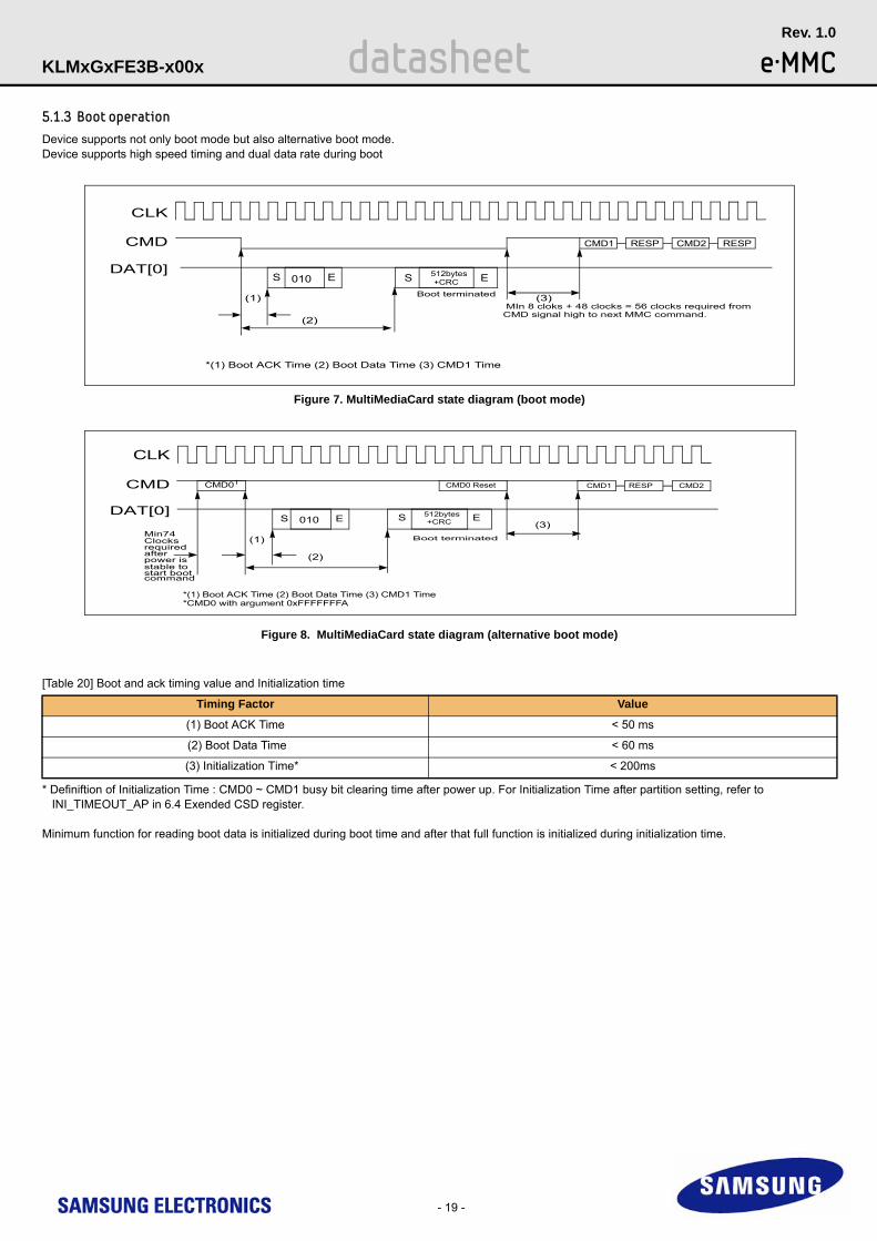
Figure 8. MultiMediaCard state diagram (alternative boot mode)
Figure 7. MultiMediaCard state diagram (boot mode)
- 19 -
datasheet e·MMCRev. 1.0
KLMxGxFE3B-x00x
5.1.3 Boot operationDevice supports not only boot mode but also alternative boot mode.Device supports high speed timing and dual data rate during boot
[Table 20] Boot and ack timing value and Initialization time
* Definiftion of Initialization Time : CMD0 ~ CMD1 busy bit clearing time after power up. For Initialization Time after partition setting, refer to INI_TIMEOUT_AP in 6.4 Exended CSD register.
Minimum function for reading boot data is initialized during boot time and after that full function is initialized during initialization time.
Timing Factor Value
(1) Boot ACK Time < 50 ms
(2) Boot Data Time < 60 ms
(3) Initialization Time* < 200ms
S E S E010512bytes+CRC
CLK
CMD
DAT[0]
CMD1 RESP CMD2 RESP
Boot terminated
MIn 8 cloks + 48 clocks = 56 clocks required fromCMD signal high to next MMC command.
(1) (3)
(2)
*(1) Boot ACK Time (2) Boot Data Time (3) CMD1 Time
S E S E010512bytes+CRC
CLK
CMD
DAT[0]
CMD1 RESP CMD2CMD01 CMD0 Reset
Min74Clocks requiredafterpower isstable to start bootcommand
*(1) Boot ACK Time (2) Boot Data Time (3) CMD1 Time*CMD0 with argument 0xFFFFFFFA
(1)
(2)
(3)
Boot terminated
CMD1
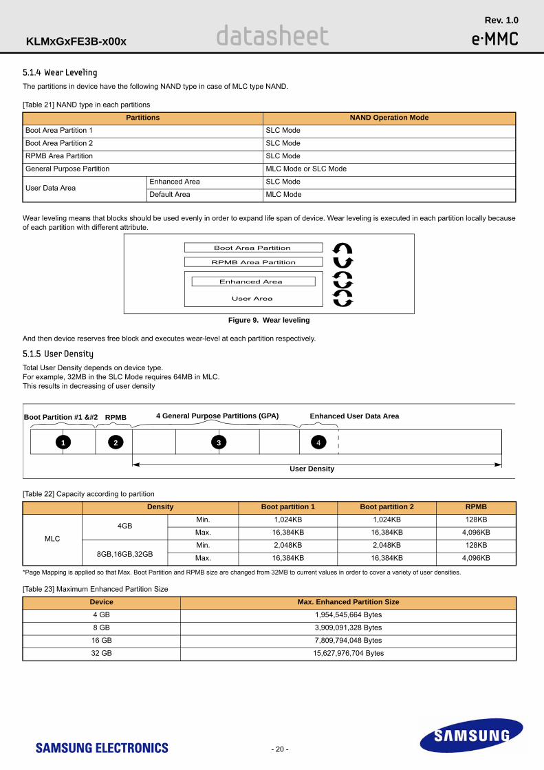
Figure 9. Wear leveling
- 20 -
datasheet e·MMCRev. 1.0
KLMxGxFE3B-x00x
5.1.4 Wear LevelingThe partitions in device have the following NAND type in case of MLC type NAND.
[Table 21] NAND type in each partitions
Wear leveling means that blocks should be used evenly in order to expand life span of device. Wear leveling is executed in each partition locally because of each partition with different attribute.
And then device reserves free block and executes wear-level at each partition respectively.
5.1.5 User DensityTotal User Density depends on device type. For example, 32MB in the SLC Mode requires 64MB in MLC. This results in decreasing of user density
[Table 22] Capacity according to partition
*Page Mapping is applied so that Max. Boot Partition and RPMB size are changed from 32MB to current values in order to cover a variety of user densities.
[Table 23] Maximum Enhanced Partition Size
Partitions NAND Operation Mode
Boot Area Partition 1 SLC Mode
Boot Area Partition 2 SLC Mode
RPMB Area Partition SLC Mode
General Purpose Partition MLC Mode or SLC Mode
User Data Area Enhanced Area SLC Mode
Default Area MLC Mode
Density Boot partition 1 Boot partition 2 RPMB
MLC
4GBMin. 1,024KB 1,024KB 128KB
Max. 16,384KB 16,384KB 4,096KB
8GB,16GB,32GBMin. 2,048KB 2,048KB 128KB
Max. 16,384KB 16,384KB 4,096KB
Device Max. Enhanced Partition Size
4 GB 1,954,545,664 Bytes
8 GB 3,909,091,328 Bytes
16 GB 7,809,794,048 Bytes
32 GB 15,627,976,704 Bytes
Boot Area Partition
RPMB Area Partition
User Area
Enhanced Area
4321
User Density
Enhanced User Data Area4 General Purpose Partitions (GPA)RPMBBoot Partition #1 
- 21 -
datasheet e·MMCRev. 1.0
KLMxGxFE3B-x00x
[Table 24] User Density Size
5.1.6 Auto Power Saving ModeIf host does not issue any command during a certain duration (1ms), after previously issued command is completed, the device enters "Power Saving mode" to reduce power consumption.
At this time, commands arriving at the device while it is in power saving mode will be serviced in normal fashion
[Table 25] Auto Power Saving Mode enter and exit
[Table 26] Auto Power Saving Mode and Sleep Mode
5.1.7 End of Life ManagementThe end of device life time is defined when there is no more available reserved block for bad block management in the device. When the deivice reaches to end of its life time, device shall change its state to permanent write protection state. In this case, write operation is not allowed any more but read oper-ation are still allowed.But, reliability of the operation can not be guaranteed after end of life
Device User Density Size
4 GB 3,909,091,328 Bytes
8 GB 7,818,182,656 Bytes
16 GB 15,634,268,160 Bytes
32 GB 31,268,536,320 Bytes
Mode Enter Condition Escape Condition
Auto Power Saving ModeWhen previous operation which came from Host is completed and no command is issued dur-ing a certain time.
If Host issues any command
Auto Power Saving Mode Sleep Mode
NAND Power ON OFF
GotoSleep Time < 1ms < 1ms
- 22 -
datasheet e·MMCRev. 1.0
KLMxGxFE3B-x00x
5.2 Smart ReportSamsung provides Report feature for the Host to notice the device state by Meta data. Samsung calls this Smart Report. So Customer can acquire prime factor for understanding at the beginning analysis of error. Below table is the information about Smart Report.
Mode Contents
5.2.1 Smart Report Sequence
Customer Report
1. Detect Error Mode2. Detect Super Block Size3. Detect Super Page Size4. Detect Optimal Write Size5. Detect Number Of Banks6.The number of Initial Bad Block, Per Bank7.The number of Init and Run Time Bad Block, Per Bank8.Number of remain block in Reserved Block 9.Max, Min, Avg Erase Count10.Number of read reclaim 11.Detect Optimal Trim Size 12.Hash code13. Max, Min, Avg Erase Count (SLC) 14. Max, Min, Avg Erase Count (MLC)
Functions Command Description
Entering Smart Report ModeCMD62h(0xEFAC62EC) → CMD62h(0xCCEE)
After entering Smart Report Mode, the report-related Values are able to be checked on Read Command.
Confirming Smart Report CMD17h(0x0) It is possible to confirm Smart Report after reading Sector 1 at Address 0.
Removing Smart Report ModeCMD62h(0xEFAC62EC)→ CMD62h(0xDECCEE)
Smart Report Mode is removed by this command.
- 23 -
datasheet e·MMCRev. 1.0
KLMxGxFE3B-x00x
5.2.2 Smart Report Output Data (For Customer)
5.2.3 Performance
* Test Condition : Bus width x8, 52MHz DDR, 100MB File Transfer, by HDBench with USB3.0 Reader, File System Overhead is included.
Data Slice
Field Width Remark
[3:0] Error Mode 4 bytes
Normal : 0xD2D2D2D2, OpenFatalError : 0x37373737, RuntimeFatalError : 0x5C5C5C5C, MetaBrokenError : 0xE1E1E1E1* In case of open error, other fields are not valid.
[7:4] Super Block Size 4 bytesTotal Size(in byte) of simultaneously erasable physical blocks(e.g., Number of Channel * N-way Interleaving * physical block size)
[11:8] Super Page Size 4 bytesTotal Size(in byte) of simultaneously programmable physical pages(e.g., Number of Channel * physical page size)
[15:12] Optimal Write Size 4 bytesWrite size(in byte) at which the device performs best(e.g., Super Page Size * N-way Interleaving)
[19:16] Number Of Banks 4 bytes Number of banks connecting to each NAND flash. Bad blocks are managed by each banks.
[23:20] Bank0 Init Bad Block 4 bytes 0
[27:24]Bank0 Init and Runtime Bad Block
4 bytesNumber of Init and Runtime defective physical blocks of plane which has the least remaining blocks in Bank0
[31:28] Bank0 remain reserved Block 4 bytes Number of remain reserved physical blocks of plane which has the least remaining blocks in Bank0
[35:32] Bank1 Init Bad Block 4 bytes 0
[39:36]Bank1 Init and Runtime Bad Block
4 bytesNumber of Init and Runtime defective physical blocks of plane which has the least remaining blocks in Bank1
[43:40] Bank1 remain reserved Block 4 bytes Number of remain reserved physical blocks of plane which has the least remaining blocks in Bank1
[47:44] Bank2 Init Bad Block 4 bytes 0
[51:48]Bank2 Init and Runtime Bad Block
4 bytesNumber of Init and Runtime defective physical blocks of plane which has the least remaining blocks in Bank2
[55:52] Bank2 remain reserved Block 4 bytes Number of remain reserved physical blocks of plane which has the least remaining blocks in Bank2
[59:56] Bank3 Init Bad Block 4 bytes 0
[63:60]Bank3 Init and Runtime Bad Block
4 bytesNumber of Init and Runtime defective physical blocks of plane which has the least remaining blocks in Bank3
[67:64] Bank3 Reserved Block 4 bytes Number of remain reserved physical blocks of plane which has the least remaining blocks in Bank3
[71:68] Max. Erase Count 4 bytes Maximum erase count from among all physical blocks
[75:72] Min. Erase Count 4 bytes Minimum erase count from among all physical blocks
[79:76] Avg. Erase Count 4 bytes Average erase count of all physical blocks
[83:80] Read Reclaim cnt 4 bytes Number of Read Reclaim Count
[87:84] Optimal Trim Size 4 bytes Optimal Trim size
[119:88] Hash Code 32 Byte Hash Code
[123:120] Max. Erase Count (SLC) 4 bytes Maximum erase count from among all SLC physical blocks
[127:124] Min. Erase Count (SLC) 4 bytes Minimum erase count from among all SLC physical blocks
[131:128] Avg. Erase Count (SLC) 4 bytes Average erase count of all SLC physical blocks
[135:132] Max. Erase Count (MLC) 4 bytes Maximum erase count from among all MLC physical blocks
[139:136] Min. Erase Count (MLC) 4 bytes Minimum erase count from among all MLC physical blocks
[143:140] Avg. Erase Count (MLC) 4 bytes Average erase count of all MLC physical blocks
[511:144] Reserved
Density Sequential Read (MB/s) Sequential Write (MB/s)
4 GB
44
8
8 GB
1416 GB
32 GB
- 24 -
datasheet e·MMCRev. 1.0
KLMxGxFE3B-x00x
6.0 REGISTER VALUE6.1 OCR RegisterThe 32-bit operation conditions register stores the VDD voltage profile of the e·MMC. In addition, this register includes a status information bit. This status bit is set if the e·MMC power up procedure has been finished. The OCR register shall be implemented by all e·MMCs.
NOTE :1) This bit is set to LOW if the e·MMC has not finished the power up routine 2) The voltage for internal flash memory(VDDF) should be 2.7-3.6v regardless of OCR Register value.
6.2 CID Register
Manufacturer ID MID 8 [127:120] 0x15
Reserved 6 [119:114] ---
Card/BGA CBX 2 [113:112] 01
OEM/Application ID OID 8 [111:104] ---1
Product name PNM 48 [103:56] See Product name table
Product revision PRV 8 [55:48] ---2
Product serial number PSN 32 [47:16] ---3
Manufacturing date MDT 8 [15:8] ---4
CRC7 checksum CRC 7 [7:1] ---5
not used, always ’1’ - 1 [0:0] ---
NOTE :1),4),5) description are same as e.MMC JEDEC standard2) PRV is composed of the revision count of controller and the revision count of F/W patch 3) A 32 bits unsigned binary integer. (Random Number)
6.2.1 Product name table (In CID Register)
OCR bit VDD voltage window2 Register Value
[6:0] Reserved 00 00000b
[7] 1.70 - 1.95 1b
[14:8] 2.0-2.6 000 0000b
[23:15] 2.7-3.6 1 1111 1111b
[28:24] Reserved 0 0000b
[30:29] Access Mode 00b (byte mode) 10b (sector mode) -[ *Higher than 2GB only]
[31] e·MMC power up status bit (busy)1
Name Field Width CID-slice CID Value
Part Number Density Product Name in CID Register (PNM)
KLM4G1FE3B-B001 4 GB 0 x 4D3447314642
KLM8G2FE3B-B001 8 GB 0 x 4D3847324642
KLMAG4FE3B-A001 16 GB 0 x 4D4147344642
KLMBG8FE3B-A001 32 GB 0 x 4D4247384642
- 25 -
datasheet e·MMCRev. 1.0
KLMxGxFE3B-x00x
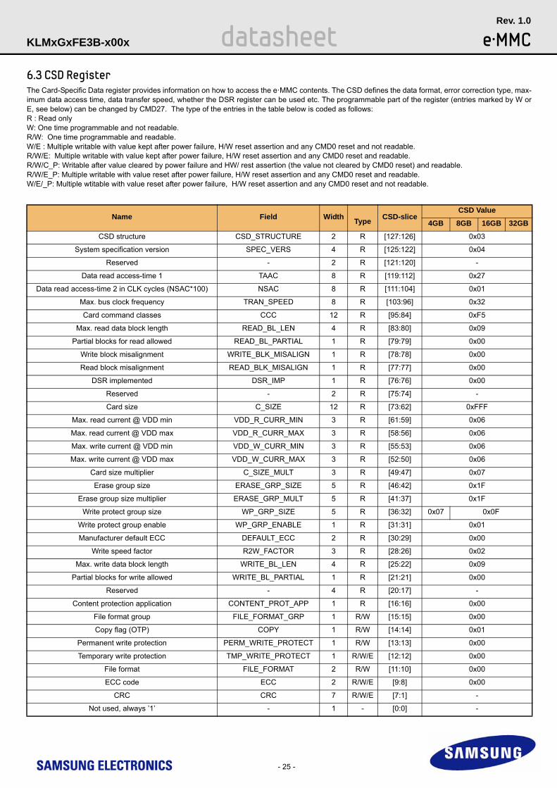
6.3 CSD RegisterThe Card-Specific Data register provides information on how to access the e·MMC contents. The CSD defines the data format, error correction type, max-imum data access time, data transfer speed, whether the DSR register can be used etc. The programmable part of the register (entries marked by W or E, see below) can be changed by CMD27. The type of the entries in the table below is coded as follows:R : Read onlyW: One time programmable and not readable.R/W: One time programmable and readable.W/E : Multiple writable with value kept after power failure, H/W reset assertion and any CMD0 reset and not readable.R/W/E: Multiple writable with value kept after power failure, H/W reset assertion and any CMD0 reset and readable.R/W/C_P: Writable after value cleared by power failure and HW/ rest assertion (the value not cleared by CMD0 reset) and readable.R/W/E_P: Multiple writable with value reset after power failure, H/W reset assertion and any CMD0 reset and readable.W/E/_P: Multiple wtitable with value reset after power failure, H/W reset assertion and any CMD0 reset and not readable.
Cell
CSD structure CSD_STRUCTURE 2 R [127:126] 0x03
System specification version SPEC_VERS 4 R [125:122] 0x04
Reserved - 2 R [121:120] -
Data read access-time 1 TAAC 8 R [119:112] 0x27
Data read access-time 2 in CLK cycles (NSAC*100) NSAC 8 R [111:104] 0x01
Max. bus clock frequency TRAN_SPEED 8 R [103:96] 0x32
Card command classes CCC 12 R [95:84] 0xF5
Max. read data block length READ_BL_LEN 4 R [83:80] 0x09
Partial blocks for read allowed READ_BL_PARTIAL 1 R [79:79] 0x00
Write block misalignment WRITE_BLK_MISALIGN 1 R [78:78] 0x00
Read block misalignment READ_BLK_MISALIGN 1 R [77:77] 0x00
DSR implemented DSR_IMP 1 R [76:76] 0x00
Reserved - 2 R [75:74] -
Card size C_SIZE 12 R [73:62] 0xFFF
Max. read current @ VDD min VDD_R_CURR_MIN 3 R [61:59] 0x06
Max. read current @ VDD max VDD_R_CURR_MAX 3 R [58:56] 0x06
Max. write current @ VDD min VDD_W_CURR_MIN 3 R [55:53] 0x06
Max. write current @ VDD max VDD_W_CURR_MAX 3 R [52:50] 0x06
Card size multiplier C_SIZE_MULT 3 R [49:47] 0x07
Erase group size ERASE_GRP_SIZE 5 R [46:42] 0x1F
Erase group size multiplier ERASE_GRP_MULT 5 R [41:37] 0x1F
Write protect group size WP_GRP_SIZE 5 R [36:32] 0x07 0x0F
Write protect group enable WP_GRP_ENABLE 1 R [31:31] 0x01
Manufacturer default ECC DEFAULT_ECC 2 R [30:29] 0x00
Write speed factor R2W_FACTOR 3 R [28:26] 0x02
Max. write data block length WRITE_BL_LEN 4 R [25:22] 0x09
Partial blocks for write allowed WRITE_BL_PARTIAL 1 R [21:21] 0x00
Reserved - 4 R [20:17] -
Content protection application CONTENT_PROT_APP 1 R [16:16] 0x00
File format group FILE_FORMAT_GRP 1 R/W [15:15] 0x00
Copy flag (OTP) COPY 1 R/W [14:14] 0x01
Permanent write protection PERM_WRITE_PROTECT 1 R/W [13:13] 0x00
Temporary write protection TMP_WRITE_PROTECT 1 R/W/E [12:12] 0x00
File format FILE_FORMAT 2 R/W [11:10] 0x00
ECC code ECC 2 R/W/E [9:8] 0x00
CRC CRC 7 R/W/E [7:1] -
Not used, always ’1’ - 1 - [0:0] -
Name Field WidthType
CSD-sliceCSD Value
4GB 8GB 16GB 32GB
- 26 -
datasheet e·MMCRev. 1.0
KLMxGxFE3B-x00x
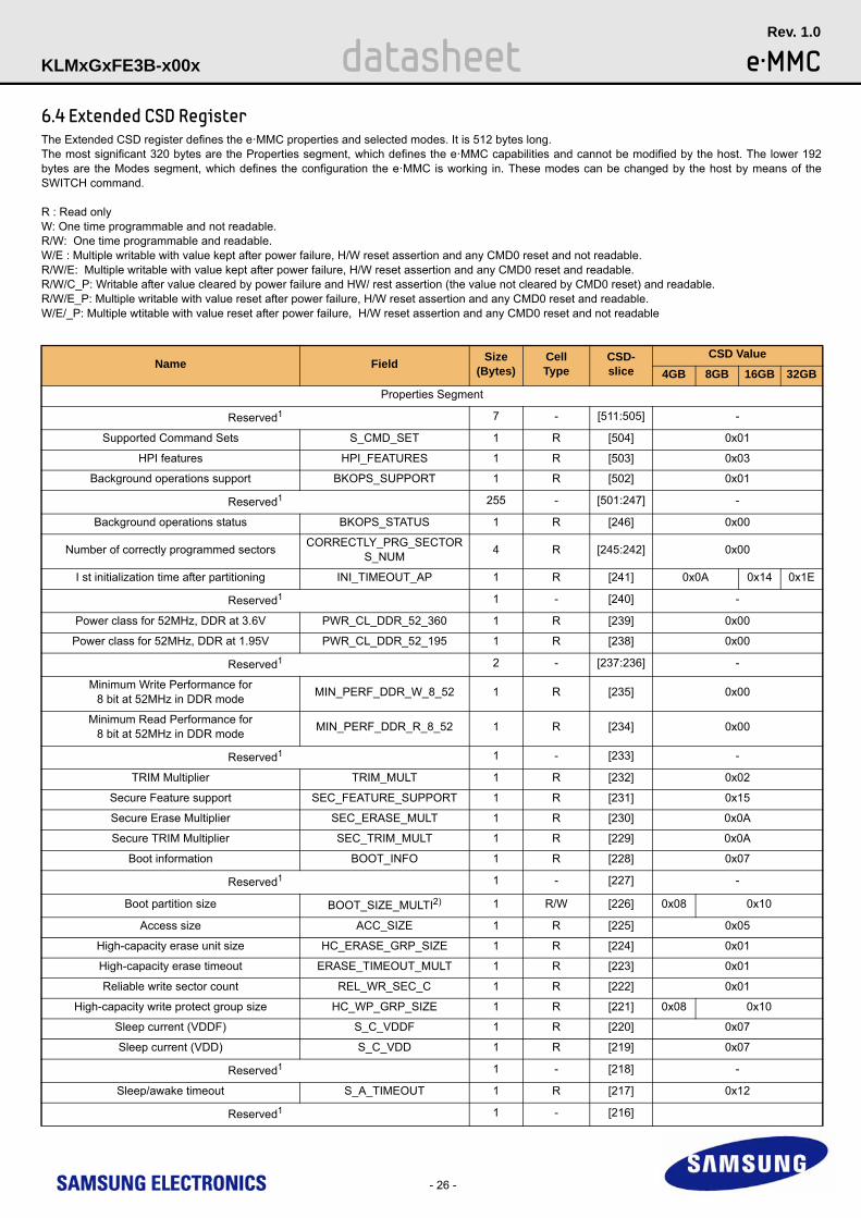
6.4 Extended CSD RegisterThe Extended CSD register defines the e·MMC properties and selected modes. It is 512 bytes long.The most significant 320 bytes are the Properties segment, which defines the e·MMC capabilities and cannot be modified by the host. The lower 192 bytes are the Modes segment, which defines the configuration the e·MMC is working in. These modes can be changed by the host by means of the SWITCH command.
R : Read onlyW: One time programmable and not readable.R/W: One time programmable and readable.W/E : Multiple writable with value kept after power failure, H/W reset assertion and any CMD0 reset and not readable.R/W/E: Multiple writable with value kept after power failure, H/W reset assertion and any CMD0 reset and readable.R/W/C_P: Writable after value cleared by power failure and HW/ rest assertion (the value not cleared by CMD0 reset) and readable.R/W/E_P: Multiple writable with value reset after power failure, H/W reset assertion and any CMD0 reset and readable.W/E/_P: Multiple wtitable with value reset after power failure, H/W reset assertion and any CMD0 reset and not readable
Name FieldSize
(Bytes)CellType
CSD-slice
CSD Value
4GB 8GB 16GB 32GB
Properties Segment
Reserved1 7 - [511:505] -
Supported Command Sets S_CMD_SET 1 R [504] 0x01
HPI features HPI_FEATURES 1 R [503] 0x03
Background operations support BKOPS_SUPPORT 1 R [502] 0x01
Reserved1 255 - [501:247] -
Background operations status BKOPS_STATUS 1 R [246] 0x00
Number of correctly programmed sectorsCORRECTLY_PRG_SECTOR
S_NUM4 R [245:242] 0x00
I st initialization time after partitioning INI_TIMEOUT_AP 1 R [241] 0x0A 0x14 0x1E
Reserved1 1 - [240] -
Power class for 52MHz, DDR at 3.6V PWR_CL_DDR_52_360 1 R [239] 0x00
Power class for 52MHz, DDR at 1.95V PWR_CL_DDR_52_195 1 R [238] 0x00
Reserved1 2 - [237:236] -
Minimum Write Performance for 8 bit at 52MHz in DDR mode
MIN_PERF_DDR_W_8_52 1 R [235] 0x00
Minimum Read Performance for8 bit at 52MHz in DDR mode
MIN_PERF_DDR_R_8_52 1 R [234] 0x00
Reserved1 1 - [233] -
TRIM Multiplier TRIM_MULT 1 R [232] 0x02
Secure Feature support SEC_FEATURE_SUPPORT 1 R [231] 0x15
Secure Erase Multiplier SEC_ERASE_MULT 1 R [230] 0x0A
Secure TRIM Multiplier SEC_TRIM_MULT 1 R [229] 0x0A
Boot information BOOT_INFO 1 R [228] 0x07
Reserved1 1 - [227] -
Boot partition size BOOT_SIZE_MULTI2) 1 R/W [226] 0x08 0x10
Access size ACC_SIZE 1 R [225] 0x05
High-capacity erase unit size HC_ERASE_GRP_SIZE 1 R [224] 0x01
High-capacity erase timeout ERASE_TIMEOUT_MULT 1 R [223] 0x01
Reliable write sector count REL_WR_SEC_C 1 R [222] 0x01
High-capacity write protect group size HC_WP_GRP_SIZE 1 R [221] 0x08 0x10
Sleep current (VDDF) S_C_VDDF 1 R [220] 0x07
Sleep current (VDD) S_C_VDD 1 R [219] 0x07
Reserved1 1 - [218] -
Sleep/awake timeout S_A_TIMEOUT 1 R [217] 0x12
Reserved1 1 - [216]
- 27 -
datasheet e·MMCRev. 1.0
KLMxGxFE3B-x00x
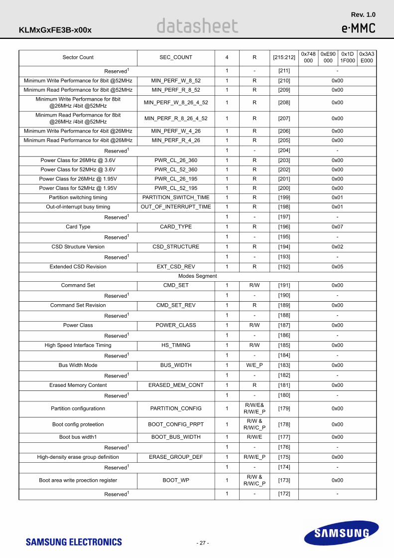
Sector Count SEC_COUNT 4 R [215:212]0x748000
0xE90000
0x1D1F000
0x3A3E000
Reserved1 1 - [211] -
Minimum Write Performance for 8bit @52MHz MIN_PERF_W_8_52 1 R [210] 0x00
Minimum Read Performance for 8bit @52MHz MIN_PERF_R_8_52 1 R [209] 0x00
Minimum Write Performance for 8bit @26MHz /4bit @52MHz
MIN_PERF_W_8_26_4_52 1 R [208] 0x00
Minimum Read Performance for 8bit @26MHz /4bit @52MHz
MIN_PERF_R_8_26_4_52 1 R [207] 0x00
Minimum Write Performance for 4bit @26MHz MIN_PERF_W_4_26 1 R [206] 0x00
Minimum Read Performance for 4bit @26MHz MIN_PERF_R_4_26 1 R [205] 0x00
Reserved1 1 - [204] -
Power Class for 26MHz @ 3.6V PWR_CL_26_360 1 R [203] 0x00
Power Class for 52MHz @ 3.6V PWR_CL_52_360 1 R [202] 0x00
Power Class for 26MHz @ 1.95V PWR_CL_26_195 1 R [201] 0x00
Power Class for 52MHz @ 1.95V PWR_CL_52_195 1 R [200] 0x00
Partition switching timing PARTITION_SWITCH_TIME 1 R [199] 0x01
Out-of-interrupt busy timing OUT_OF_INTERRUPT_TIME 1 R [198] 0x01
Reserved1 1 - [197] -
Card Type CARD_TYPE 1 R [196] 0x07
Reserved1 1 - [195] -
CSD Structure Version CSD_STRUCTURE 1 R [194] 0x02
Reserved1 1 - [193] -
Extended CSD Revision EXT_CSD_REV 1 R [192] 0x05
Modes Segment
Command Set CMD_SET 1 R/W [191] 0x00
Reserved1 1 - [190] -
Command Set Revision CMD_SET_REV 1 R [189] 0x00
Reserved1 1 - [188] -
Power Class POWER_CLASS 1 R/W [187] 0x00
Reserved1 1 - [186] -
High Speed Interface Timing HS_TIMING 1 R/W [185] 0x00
Reserved1 1 - [184] -
Bus Width Mode BUS_WIDTH 1 W/E_P [183] 0x00
Reserved1 1 - [182] -
Erased Memory Content ERASED_MEM_CONT 1 R [181] 0x00
Reserved1 1 - [180] -
Partition configurationn PARTITION_CONFIG 1R/W/E&
R/W/E_P[179] 0x00
Boot config proteetion BOOT_CONFIG_PRPT 1R/W &
R/W/C_P[178] 0x00
Boot bus width1 BOOT_BUS_WIDTH 1 R/W/E [177] 0x00
Reserved1 1 - [176] -
High-density erase group definition ERASE_GROUP_DEF 1 R/W/E_P [175] 0x00
Reserved1 1 - [174] -
Boot area write proection register BOOT_WP 1R/W &
R/W/C_P[173] 0x00
Reserved1 1 - [172] -
- 28 -
datasheet e·MMCRev. 1.0
KLMxGxFE3B-x00x
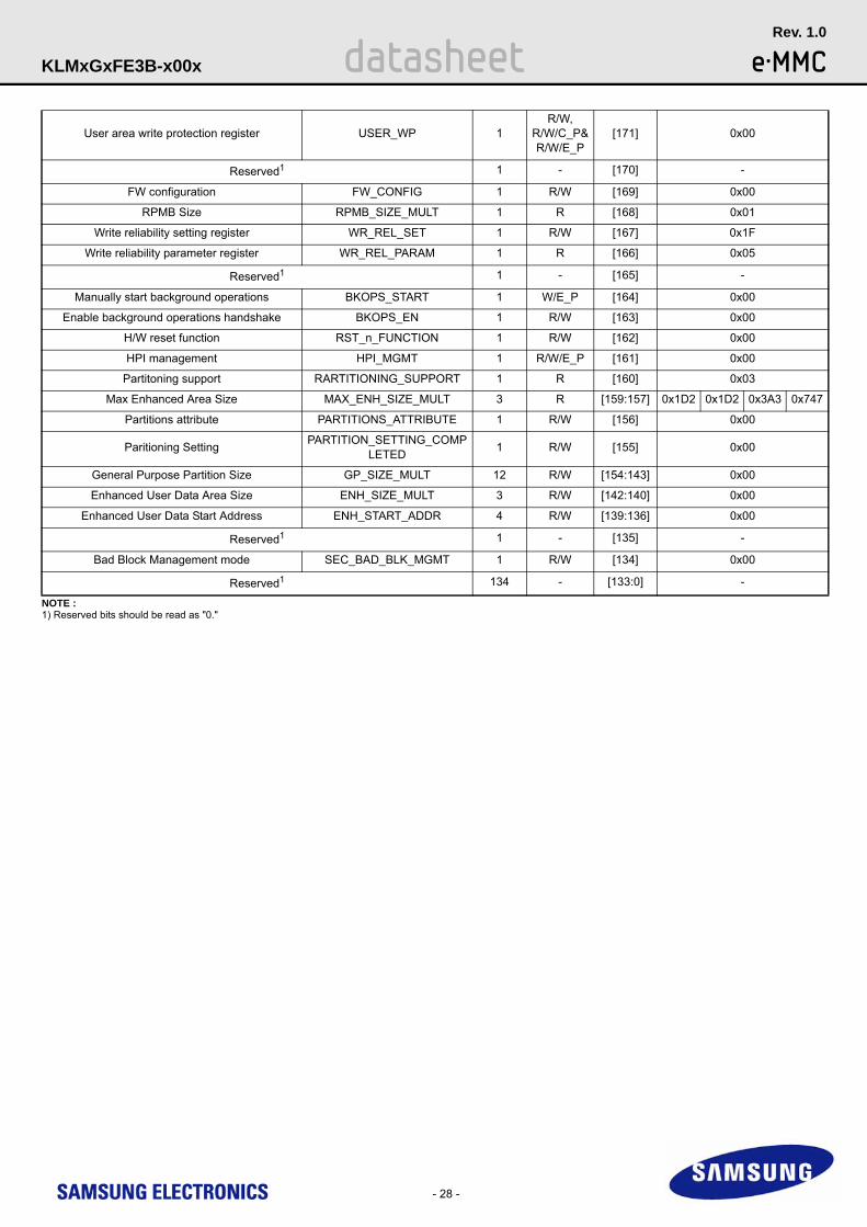
NOTE :1) Reserved bits should be read as "0."
User area write protection register USER_WP 1R/W,
R/W/C_P&R/W/E_P
[171] 0x00
Reserved1 1 - [170] -
FW configuration FW_CONFIG 1 R/W [169] 0x00
RPMB Size RPMB_SIZE_MULT 1 R [168] 0x01
Write reliability setting register WR_REL_SET 1 R/W [167] 0x1F
Write reliability parameter register WR_REL_PARAM 1 R [166] 0x05
Reserved1 1 - [165] -
Manually start background operations BKOPS_START 1 W/E_P [164] 0x00
Enable background operations handshake BKOPS_EN 1 R/W [163] 0x00
H/W reset function RST_n_FUNCTION 1 R/W [162] 0x00
HPI management HPI_MGMT 1 R/W/E_P [161] 0x00
Partitoning support RARTITIONING_SUPPORT 1 R [160] 0x03
Max Enhanced Area Size MAX_ENH_SIZE_MULT 3 R [159:157] 0x1D2 0x1D2 0x3A3 0x747
Partitions attribute PARTITIONS_ATTRIBUTE 1 R/W [156] 0x00
Paritioning SettingPARTITION_SETTING_COMP
LETED1 R/W [155] 0x00
General Purpose Partition Size GP_SIZE_MULT 12 R/W [154:143] 0x00
Enhanced User Data Area Size ENH_SIZE_MULT 3 R/W [142:140] 0x00
Enhanced User Data Start Address ENH_START_ADDR 4 R/W [139:136] 0x00
Reserved1 1 - [135] -
Bad Block Management mode SEC_BAD_BLK_MGMT 1 R/W [134] 0x00
Reserved1 134 - [133:0] -
- 29 -
datasheet e·MMCRev. 1.0
KLMxGxFE3B-x00x
7.0 AC PARAMETER7.1 Time Parameter
s
ms
Write Timeout 350 ms
Erase Timeout 10 ms
Force Erase Timeout 3 min
Secure Erase Timeout 3 s
Secure Trim step1 Timeout 1) 600 ms
Secure Trim step2 Timeout 3 s
Trim Timeout 1) 600 ms
Partition Switching Timeout (after Init) 100 us
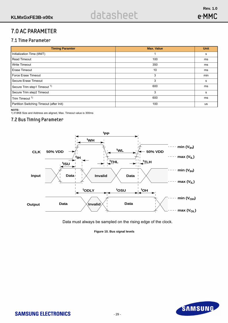
Figure 10. Bus signal levels
NOTE:1) If 8KB Size and Address are aligned, Max. Timeout value is 300ms
7.2 Bus Timing Parameter
Timing Paramter Max. Value Unit
Initialization Time (tINIT) 1
Read Timeout 100
Data Data
Data
Invalid
Invalid
tPP
tWH
tWL
tISU
tIHtTHL tTLH
tOH
CLK
Input
Output
Data must always be sampled on the rising edge of the clock.
tOSUtODLY
50% VDD50% VDD
min (VIH)
min (VOH)
max (VIL)
min (VIH)
max (VIL)
max (VOL)
Data
- 30 -
datasheet e·MMCRev. 1.0
KLMxGxFE3B-x00x
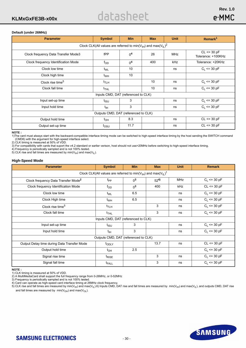
Default (under 26MHz)
NOTE :1)The card must always start with the backward-compatible interface timing mode can be switched to high-speed interface timing by the host sending the SWITCH command (CMD6) with the argument for high-speed interface select.2) CLK timing is measured at 50% of VDD.3) For compatibility with cards that suport the v4.2 standard or earlier verison, host should not use>20MHz before switching to high-speed interface timing.4) Frequency is periodically sampled and is not 100% tested.5) CLK rise and fall times are measured by min(VIH) and max(VIL).
High-Speed Mode
NOTE :1) CLK timing is measured at 50% of VDD.2) A MultiMediaCard shall support the full frequency range from 0-26MHz, or 0-52MHz3) Frequency is periodically sampled and is not 100% tested.4) Card can operate as high-speed card interface timing at 26MHz clock frequency.5) CLK rise and fall times are measured by min(VIH) and max(VIL).6) Inputs CMD, DAT rise and fall times are measured by min(VIH) and max(VIL), and outputs CMD, DAT rise
and fall times are measured by min(VOH) and max(VOL).
Parameter Symbol Min Max Unit Remark1
Clock CLK(All values are referred to min(VIH) and max(VIL)2
Clock frequency Data Transfer Mode3 fPP 04 26 MHzCL <= 30 pF
Tolerance: +100KHz
Clock frequency Identification Mode fOD 04 400 kHz Tolerance: +20KHz
Clock low time tWL 10 ns CL <= 30 pF
Clock high time tWH 10
Clock rise time5 tTLH 10 ns CL <= 30 pF
Clock fall time tTHL 10 ns CL <= 30 pF
Inputs CMD, DAT (referenced to CLK)
Input set-up time tISU 3 ns CL <= 30 pF
Input hold time tIH 3 ns CL <= 30 pF
Outputs CMD, DAT (referenced to CLK)
Output hold time tOH 8.3 ns CL <= 30 pF
Output set-up time tOSU 11.7 ns CL <= 30 pF
Parameter Symbol Min Max Unit Remark
Clock CLK(All values are referred to min(VIH) and max(VIL)1
Clock frequency Data Transfer Mode2 fPP 03 524) MHz CL <= 30 pF
Clock frequency Identification Mode fOD 03 400 kHz CL <= 30 pF
Clock low time tWL 6.5 ns CL <= 30 pF
Clock High time tWH 6.5 ns CL <= 30 pF
Clock rise time5 tTLH 3 ns CL <= 30 pF
Clock fall time tTHL 3 ns CL <= 30 pF
Inputs CMD, DAT (referenced to CLK)
Input set-up time tISU 3 ns CL <= 30 pF
Input hold time tIH 3 ns CL <= 30 pF
Outputs CMD, DAT (referenced to CLK)
Output Delay time during Data Transfer Mode tODLY 13.7 ns CL <= 30 pF
Output hold time tOH 2.5 CL <= 30 pF
Signal rise time tRISE 3 ns CL <= 30 pF
Signal fall time tFALL 3 ns CL <= 30 pF
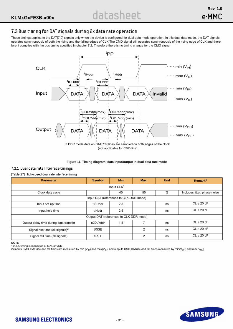
Figure 11. Timing diagram: data input/output in dual data rate mode
- 31 -
datasheet e·MMCRev. 1.0
KLMxGxFE3B-x00x
7.3 Bus timing for DAT signals during 2x data rate operationThese timings applies to the DAT[7:0] signals only when the device is configured for dual data mode operation. In this dual data mode, the DAT signals operates synchronously of both the rising and the falling edges of CLK.The CMD signal still operates synchronously of the rising edge of CLK and therefore it complies with the bus timing specified in chapter 7.2, Therefore there is no timing change for the CMD signal
7.3.1 Dual data rate interface timings[Table 27] High-speed dual rate interface timing
NOTE :1) CLK timing is measuted at 50% of VDD2) Inputs CMD, DAT rise and fall times are measured by min (VIH) and max(VIL), and outputs CMD,DATrise and fall times measured by min(VOH) and max(VOL)
Parameter Symbol Min Max. Unit Remark1
Input CLK1
Clock duty cycle 45 55 % Includes jitter, phase noise
Input DAT (referenced to CLK-DDR mode)
Input set-up time tISUddr 2.5 ns CL 20 pF
Input hold time tIHddr 2.5 ns CL 20 pF
Output DAT (referenced to CLK-DDR mode)
Output delay time during data transfer tODLYddr 1.5 7 ns CL 20 pF
Signal rise time (all signals)2 tRISE 2 ns CL 20 pF
Signal fall time (all signals) tFALL 2 ns CL 20 pF
DATA
tPP
tISUddr
Input
Output
In DDR mode data on DAT[7:0] lines are sampled on both edges of the clock
tODLYddr(max)
min (VIH)
min (VOH)
max (VIL)
min (VIH)
max (VIL)
max (VOL)
CLK
DATA DATA Invalid
tIHddr
tISUddr
tIHddr
I DATA DATA DATA
tODLYddr(min)
tODLYddr(max)
tODLYddr(min)
(not applicable for CMD line)
- 32 -
datasheet e·MMCRev. 1.0
KLMxGxFE3B-x00x
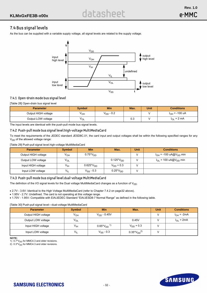
7.4 Bus signal levelsAs the bus can be supplied with a variable supply voltage, all signal levels are related to the supply voltage.
7.4.1 Open-drain mode bus signal level[Table 28] Open-drain bus signal level
The input levels are identical with the push-pull mode bus signal levels.
7.4.2 Push-pull mode bus signal level.high-voltage MultiMediaCardTo meet the requirements of the JEDEC standard JESD8C.01, the card input and output voltages shall be within the following specified ranges for any VDD of the allowed voltage range:
[Table 29] Push-pull signal level.high-voltage MultiMediaCard
7.4.3 Push-pull mode bus signal level.dual-voltage MultiMediaCardThe definition of the I/O signal levels for the Dual voltage MultiMediaCard changes as a function of VDD.
2.7V - 3.6V: Identical to the High Voltage MultiMediaCard (refer to Chapter 7.4.2 on page32 above). 1.95V - 2.7V: Undefined. The card is not operating at this voltage range.1.70V - 1.95V: Compatible with EIA/JEDEC Standard “EIA/JESD8-7 Normal Range” as defined in the following table.
[Table 30] Push-pull signal level—dual-voltage MultiMediaCard
NOTE:1) 0.7*VDD for MMC4.3 and older revisions.2) 0.3*VDD for MMC4.3 and older revisions.
Parameter Symbol Min Max. Unit Conditions
Output HIGH voltage VOH VDD - 0.2 V IOH = -100 uA
Output LOW voltage VOL 0.3 V IOL = 2 mA
Parameter Symbol Min Max. Unit Conditions
Output HIGH voltage VOH 0.75*VDD V IOH = -100 uA@VDD min
Output LOW voltage VOL 0.125*VDD V IOL = 100 uA@VDD min
Input HIGH voltage VIH 0.625*VDD VDD + 0.3 V
Input LOW voltage VIL VSS - 0.3 0.25*VDD V
Parameter Symbol Min Max. Unit Conditions
Output HIGH voltage VOH VDD - 0.45V V IOH = -2mA
Output LOW voltage VOL 0.45V V IOL = 2mA
Input HIGH voltage VIH 0.65*VDD 1) VDD + 0.3 V
Input LOW voltage VIL VSS - 0.3 0.35*VDD2) V
V
t
inputhigh level
inputlow level
outputhigh level
outputlow level
undefined
VDD
VIH
VOH
VIL
VSS
VOL
- 33 -
datasheet e·MMCRev. 1.0
KLMxGxFE3B-x00x
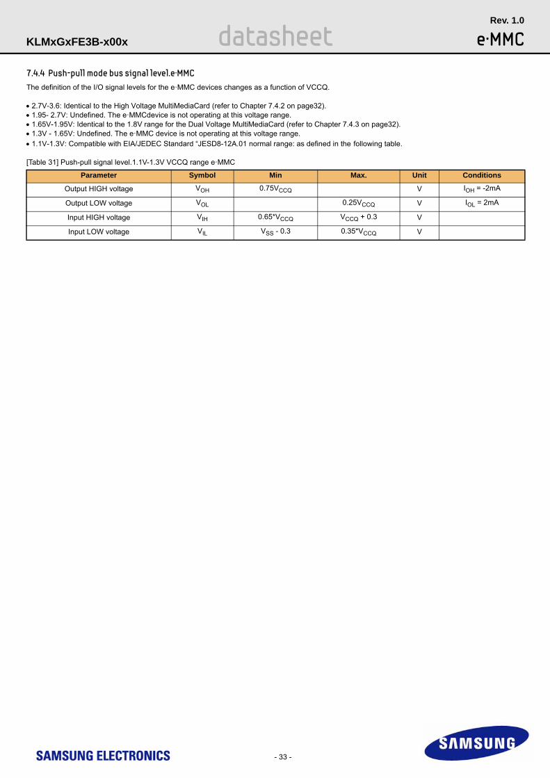
7.4.4 Push-pull mode bus signal level.e·MMCThe definition of the I/O signal levels for the e·MMC devices changes as a function of VCCQ.
2.7V-3.6: Identical to the High Voltage MultiMediaCard (refer to Chapter 7.4.2 on page32).1.95- 2.7V: Undefined. The e·MMCdevice is not operating at this voltage range.1.65V-1.95V: Identical to the 1.8V range for the Dual Voltage MultiMediaCard (refer to Chapter 7.4.3 on page32).1.3V - 1.65V: Undefined. The e·MMC device is not operating at this voltage range.1.1V-1.3V: Compatible with EIA/JEDEC Standard “JESD8-12A.01 normal range: as defined in the following table.
[Table 31] Push-pull signal level.1.1V-1.3V VCCQ range e·MMC
Parameter Symbol Min Max. Unit Conditions
Output HIGH voltage VOH 0.75VCCQ V IOH = -2mA
Output LOW voltage VOL 0.25VCCQ V IOL = 2mA
Input HIGH voltage VIH 0.65*VCCQ VCCQ + 0.3 V
Input LOW voltage VIL VSS - 0.3 0.35*VCCQ V
- 34 -
datasheet e·MMCRev. 1.0
KLMxGxFE3B-x00x
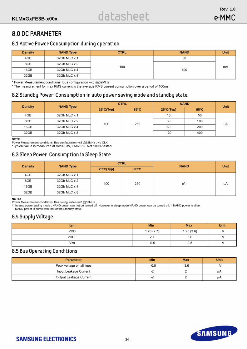
8.0 DC PARAMETER8.1 Active Power Consumption during operation
* Power Measurement conditions: Bus configuration =x8 @52MHz* The measurement for max RMS current is the average RMS current consumption over a period of 100ms.
8.2 Standby Power Consumption in auto power saving mode and standby state.
NOTE:Power Measurement conditions: Bus configuration =x8 @52MHz , No CLK*Typical value is measured at Vcc=3.3V, TA=25°C. Not 100% tested.
8.3 Sleep Power Consumption in Sleep State
NOTE:Power Measurement conditions: Bus configuration =x8 @52MHz , 1) In auto power saving mode , NAND power can not be turned off .However in sleep mode NAND power can be turned off. If NAND power is alive , NAND power is same with that of the Standby state.
8.4 Supply Voltage
8.5 Bus Operating Conditions
-2 2 A
-2 2 A
Density NAND Type CTRL NAND Unit
4GB 32Gb MLC x 1
100
50
mA8GB 32Gb MLC x 2
10016GB 32Gb MLC x 4
32GB 32Gb MLC x 8
Density NAND Type CTRL NAND
Unit25C(Typ) 85C 25C(Typ) 85C
4GB 32Gb MLC x 1
100 250
15 50
uA8GB 32Gb MLC x 2 30 100
16GB 32Gb MLC x 4 60 200
32GB 32Gb MLC x 8 120 400
Density NAND TypeCTRL
NAND Unit25C(Typ) 85C
4GB 32Gb MLC x 1
100 250 01) uA8GB 32Gb MLC x 2
16GB 32Gb MLC x 4
32GB 32Gb MLC x 8
Item Min Max Unit
VDD 1.70 (2.7) 1.95 (3.6) V
VDDF 2.7 3.6 V
Vss -0.5 0.5 V
Parameter Min Max Unit
Peak voltage on all lines -0.5 3.6 V
Input Leakage Current
Output Leakage Current
- 35 -
datasheet e·MMCRev. 1.0
KLMxGxFE3B-x00x
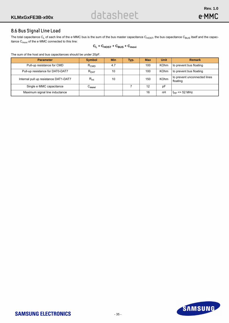
8.6 Bus Signal Line LoadThe total capacitance CL of each line of the e·MMC bus is the sum of the bus master capacitance CHOST, the bus capacitance CBUS itself and the capac-
itance Cmovi of the e·MMC connected to this line:
CL = CHOST + CBUS + Cmovi
The sum of the host and bus capacitances should be under 20pF.
Pull-up resistance for CMD RCMD 4.7 100 KOhm to prevent bus floating
Pull-up resistance for DAT0-DAT7 RDAT 10 100 KOhm to prevent bus floating
Internal pull up resistance DAT1-DAT7 Rint 10 150 KOhmto prevent unconnected lines floating
Single e·MMC capacitance Cmovi 7 12 pF
Maximum signal line inductance 16 nH fPP <= 52 MHz
Parameter Symbol Min Typ. Max Unit Remark
- 36 -
datasheet e·MMCRev. 1.0
KLMxGxFE3B-x00x
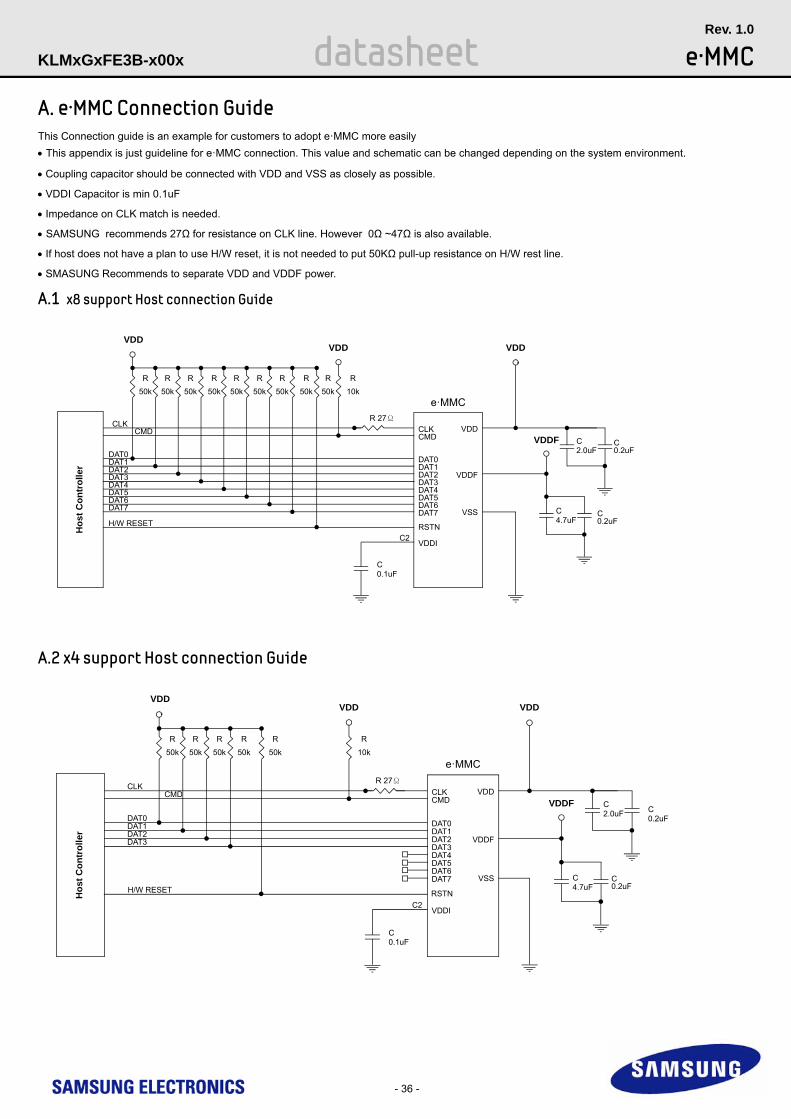
A. e·MMC Connection GuideThis Connection guide is an example for customers to adopt e·MMC more easily
This appendix is just guideline for e·MMC connection. This value and schematic can be changed depending on the system environment.
Coupling capacitor should be connected with VDD and VSS as closely as possible.
VDDI Capacitor is min 0.1uF
Impedance on CLK match is needed.
SAMSUNG recommends 27Ω for resistance on CLK line. However 0Ω ~47Ω is also available.
If host does not have a plan to use H/W reset, it is not needed to put 50KΩ pull-up resistance on H/W rest line.
SMASUNG Recommends to separate VDD and VDDF power.
A.1 x8 support Host connection Guide
A.2 x4 support Host connection Guide
e·MMC
VDDF C2.0uF
C0.1uF
Ho
st C
on
tro
ller
VDDVDD
VDD
CMDCLK
DAT0DAT1DAT2DAT3DAT4DAT5DAT6DAT7
R
50k
R
50k
R
50k
R
50k
R
50k
R
50k
R
50k
R
50k
R
10k
R 27Ω
DAT0DAT1DAT2DAT3DAT4DAT5DAT6DAT7
CMDCLK
VDDF
VDD
VSS
VDDIC2
RSTNH/W RESET
R
50k
C0.2uF
C4.7uF
C0.2uF
e·MMC
VDDFC0.2uF
C2.0uF
C0.1uF
Ho
st C
on
tro
ller
VDDVDD
VDD
CMDCLK
DAT0DAT1DAT2DAT3
R
50k
R
50k
R
50k
R
50k
R
10k
R 27Ω
DAT0DAT1DAT2DAT3DAT4DAT5DAT6DAT7
CMDCLK
VDDF
VDD
VSS
VDDIC2
RSTNH/W RESET
R
50k
C0.2uF
C4.7uF