Embed Size (px)
Citation preview

Design and Development of Low-Cost …………….. Samuel Farayola.Kolawole, D.S. Nyitamen, M.K Barau
website: www.academyjsekad.edu.ng
DESIGN AND DEVELOPMENT OF LOW-COST HANDHELD OSCILLOSCOPE
Samuel Farayola Kolawole1, D.S. Nyitamen1, M.K Barau2 1Department of Electrical//Electronic Engineering, Nigerian Defence Academy, Kaduna
2Kaduna Refining and Petrochemical Company, Kaduna
Abstract
The paper presents the design and development of a portable and-held digital oscilloscope using Atmel
Atmega644p Microcontroller Unit operating at 20MHz & 20MIPS on a mono chrome Graphical Liquid
Crystal Display. The oscilloscope has two channels through which the controller samples the analog input
signals. AC & DC signals are fed to the controller’s ADC for conversion into its digital equivalents. The
sampled signals undergo processes of pre-scaling, filtration, storage, reconstruction and then displayed on the
GLCD. The microcontroller is programmed using BASCOM-AVR, a BASIC programming language-based
Integrated Development Environment (IDE) The Oscilloscope can display the scaling factor used in readable
format in Volts/div for the vertical axis and Time/div for the horizontal axis. It can also display measured
signals from the two channels simultaneously and has channels offset control and trigger mode adjusting. The
handy Oscilloscope has the capability of displaying the measured signal frequency value in the range of 0-
250kHz. Some signal types were measured and compared with the laboratory oscilloscope and produced an
error of less than 5%. The cost of the hand-held oscilloscope was N12,410, which is less than $50, hence it is
low-cost compared with commercially available digital oscilloscope.
Keywords: A/D Conversion, ATMega644P Microcontroller, Oscilloscope, Pre-scaling, Sampling,
Transducer.
1.0 INTRODUCTION
In many applications, observing certain
voltage waveforms in a circuit plays a crucial
role in understanding the operation of the
circuit. For that purpose several measuring
instruments are used like voltmeter, ammeter,
or the oscilloscope. An oscilloscope is a
voltage sensing electronic instrument that is
used to visualize certain voltage waveforms
(Banf, 2011). An oscilloscope displays the
variation of a voltage waveform in time on the
oscilloscope’s screen graphically. Digital
oscilloscopes are quickly replacing Cathode
Ray Oscilloscopes (CRO) because of their
inherently high input impedance and small
size. (Chandan, 2004). Most oscilloscopes
have at least two input channels and each
channel can display a waveform on the screen.
Multiple channels are useful for comparing
waveforms. For example, one can observe the
voltage waveforms at the input and the output
terminals of a circuit simultaneously, by using
a two channel oscilloscope.
Special-purpose oscilloscopes may be used for
such purposes as analysing an automotive
ignition system or to display the waveform of
the heartbeat as in Electrocardiogram.
Cathode Ray Oscilloscopes are expensive and
bulky, there is always a need to develop
systems that are portable. Celma (1992),
Chandan (2016) and Shilpa (2016) developed
PC-based Oscilloscopes which can be used
instead of the expensive CRO, however, these
will require a computer. Recent research
efforts are on developing small size
oscilloscopes. (Additi, 2014; Bhagashree
2015;Hua. 2011; Ishitak 2014; Shepherd 2001;
Yogesh 2014.)
This paper is aimed at designing and
developing a low cost Microcontroller-based
‘Hand-held Oscilloscope’, using Graphic
Liquid Crystal Display (GLCD) to display the
output.

Design and Development of Low-Cost …………….. Samuel Farayola.Kolawole, D.S. Nyitamen, M.K Barau
Academy Journal of Science and Engineering 10 (1), 2016 Page 53
2.0 METHODOLOGY
Fig.1 shows the block diagram for the
handheld Oscilloscope.A dc source is used to
power the system. The input signals on two
channels are voltage signals. If the physical
quantity is not in voltage form,
transducers/sensors would have been used to
convert the physical quantity into a voltage
signal. Pre-scaling and filtering takes place on
the signal before it is fed into an ATmega644P
8-bit AVR Microcontroller. The micro-
controller has ADC which samples and codes
the analog signal. The microcontroller sends
digital form of the analog signal to the GLCD
where the signal is reconstructed and
displayed. A Key-pad is attached to the
microcontroller for the purpose of choosing
channel and scale and other operations of
moving the waveform up-down or left-right.
2.1 HARDWARE DESIGN
2.1.1 Input Signal Attenuator/Scaler
The attenuation of any input signal voltages
particularly those with higher amplitude
voltages was achieved using the combination
of input resistors network providing potential
divider arrangement with CMOS analog
multiplexer IC [TC4052B] (U1,U2).
Toshiba TC4052B is a high speed, differential
4-channel CMOS analog Multiplexer/De-
multiplexer ICthat has two binary control
inputs (A and B) and an inhibitinput. The two
binary input signals select one of four pairs
(X0Y0, X1Y1, X2Y2, X3Y3,) of channels to be
turned on and connect the analoginputs to the
respective outputs (X-out & Y-out).
Also anotheranalog multiplexer IC (U2)
provides another function of switching DC/AC
signals. The analog multiplexer IC requires a
voltage supply of ±5V in order to respond to
the AC waveform.
Input
Fig. 1 Block Diagram of Handheld Oscilloscope
Micro
controller Unit
Analog-to-
Digital
Converter GLCD Controller
Driver
Graphic LCD
Screen
I/P Signal Attnuator
Power Supply Unit
Crystal Oscillator
Key Board Unit

Design and Development of Low-Cost …………….. Samuel Farayola.Kolawole, D.S. Nyitamen, M.K Barau
Academy Journal of Science and Engineering 10 (1), 2016 Page 54
2.1.2 Channel Selection and Scaling
In order to provide a calibrated trace on the
display, input attenuators must have very
accurate resistive networks that have a flat
response over the whole oscilloscope
bandwidth. Three pairs of potential divider
arrangements of resistors were established at
the oscilloscope input for scaling the signals
connected across the probes. The control
inputs A, B of the TC4052B analog
multiplexer IC are connected to the
microcontroller which select the needed (train
of potential divider) factor to scale input
signal.
Table 1 Truth Table of TC4052B IC (U1)
X=Don’t care
The combination of the resistors with
TC4052Banalog multiplexer switch is to
configure the attenuator input sensitivity to
supports 10V, 25V and 50V on a scale factors
of 1/2, 1/5, and 1/10 respectively, whereas the
pre-scaling for lower input voltages 0.25V,
0.5V & 1V is done through the software.
2.1.2.1 DC Input Signal Scaling (Channel X)
The input signal to be measured under goes a
pre-scaling, (Fig. 2) before it is fed to the
microcontroller’s ADC. The resistors network
formed three (3) independent potential divider
configurations, with each connected to the (3
out of 4) of Multiplexer’s channels to the
ground via the IC’s internal resistance (Ron)
and the common output.
For input X3
Fig. 2 Pre-Scaling Resistor Divider
Control Inputs Output Channel Scale Factor
B A
(PA0) (PA1)
INH XoutYout
0 0 0 X0 , Y0 NC
0 1 0 X1 , Y1 X 1/2
1 0 0 X2 , Y2 X 1/5
1 1 0 X3 , Y3 X 1/10
XX 1 None, None None
TC4052B
PA1 PA0
To PA4, ADC
R1
R2
X com
X1
X2
X3
Signal input (V)
Ron
1
10
50V max

Design and Development of Low-Cost …………….. Samuel Farayola.Kolawole, D.S. Nyitamen, M.K Barau
Academy Journal of Science and Engineering 10 (1), 2016 Page 55
Using a scale factor of 1
10
Let R1 be = 10 kΩ
And Ronfrom TC4052B data sheet was given
to be 60Ω (at 5V, 40oC)
Therefore,
Using Voltage Divider Rule, 1
10𝑉 =
R2 + Ron
R1 +R2 + Ron𝑉
R2 = 1051.11Ω ≈ 1051Ω or 1.051kΩ, i.e.
1000Ω + 51Ω
For input X2
Let the scale factor be = 1
5
R2 = 2440Ω ≈ 2400Ω or 2.4kΩ (the nearest
standard value).
For input X1
Let the scale factor be = 1
2
R4 = 9940Ω ≈ 10000Ω or 10kΩ (being the
nearest standard value).
2.1.2.2 DC Input Signal Scaling (Channel Y)
The same analysis applied for oscilloscope
channel 2 using Y- channel of the analog
Multiplexers Q1 and Q2, for the D.C. and A.C
waveforms. The exception here is that, Ycom
output of IC Q2 goes to microcontroller port
PA5, (See the truth table above).
2.1.2.3AC/DC Signal Selection (Channel X),
IC[TC4052B] U2
In order to read and reconstruct A.C.
waveform another multiplexer [TC4052B]
(U2) is used via capacitor connected in series,
and also for A.C. / D.C. selection. For D.C.
input signal the MUX is switched to by-pass
the capacitor, while for the A.C. signal type it
goes straight through the capacitor. In addition
to the AC input signal, the MUX was also
equipped with a fixed offset voltage of 2.5V
via a 1.0 MΩ resistor for current limiting.
Table 2 is the truth table for the selection.
Table 2: Truth Table for AC/DC selection, TC4052B IC (U2)
X = Don’t care
2.1.3Analog-to-Digital Converter ADC
In the real world, most data is characterized by
analog signals. In order to manipulate the data
using a microprocessor, we need to convert
the analog signals to its digital equivalent, so
that the microprocessor will be able to read,
understand and manipulate the data.3The main
goal of A/D Converter is to digitize the analog
signals, which means to read, store and
produce at its output the analog signals in
numbers (binary).
2.1.3.1Sampling Ratefs
The analog signal is continuous in time and it
is necessary to convert this to a flow of digital
values. It is therefore required to define the
rate at which new digital values are sampled
from the analog signal. The rate of new values
is called the sampling rate or sampling
frequency of the converter (the number of
samples taken in a second).
Control Inputs Output Channel Scale Factor
B A
(PA2)(PA3)
INH XoutYout
0 0 0 X0 , Y0 XDC, YDC
0 1 0 X1 , Y1 Xoffset , YDC
1 0 0 X2 , Y2 XDC , Yoffset
1 1 0 X3 , Y3 Xoffset , Yoffset
XX 1 None, None None

Design and Development of Low-Cost …………….. Samuel Farayola.Kolawole, D.S. Nyitamen, M.K Barau
Academy Journal of Science and Engineering 10 (1), 2016 Page 56
A continuously varying, band limited signal
can be sampled (that is, the signal values at
intervals of time T, the sampling time, are
measured and stored) and then the original
signal can be exactly reproduced from the
discrete-time values by an inter-
polation formula. The accuracy is limited by
quantization error. However, this faithful
reproduction is only possible if the sampling
rate is higher than twice the highest frequency
of the signal. This is essentially what is
embodied in the Shannon-Nyquist sampling
theorem
2.1.4 Selection of the Microcontroller
The ATmega644 AVR microcontroller was
chosen for the microcomputer unit of this
work instead of a PIC (Programmable
Interface Controller) or Arduino module due
to its wide range of applications such as higher
memory size and better processing speed (one
instruction/clock cycle), pulse width
modulation (PWM) capabilities, digital signal
processing (DSP), multiple I/O ports (up to 5
I/O ports),. Other factors that have driven the
selection of the AVR microcontroller
(Atmega644P) are low cost, versatility, ease of
programming, and small size. The
ATmega644P architecture is based on the
Reduced Instruction Set Computer (RISC)
concept which allows the processor to
complete 20 million instructions per second
(MIPS) when operating at 20MHz.
Atmel's AVR microcontrollers use a new
RISC architecture which has been developed
to take advantage of the semiconductor
integration and software capabilities of the
1990's. The resulting micro controllers offer
the highest MIPS/mW capability available in
the 8-bit micro controllers market today.
The architecture of the AVR microcontrollers
was designed together with C-language
experts to ensure that the hardware and
software work hand-in-hand to develop a
highly efficient, high-performance code. The
family of AVR microcontrollers includes
differently equipped controllers - from a
simple 8-pin microcontroller up to a high-end
microcontroller with a large internal memory.
2.1.5 The Key Board Unit
The normal execution of the program follows
a designated sequence of instructions.
However, some times this normal sequence of
events must be interrupted to respond to high
priority faults and status both inside and
outside the micro controller. When these
higher priority events occur, the
microcontroller must temporarily suspend
normal operation and execute event specific
actions called an interrupt service routine.
Once the higher priority event has been
serviced, the microcontroller returns and
continues processing the normal program.
Those higher priority interrupts and other
unconditional calls are provided by the use of
some set of press button switches called the
Key Board Unit. The microcontroller used in
this project is equipped with a complement of
26 interrupt sources. Two of the interrupts are
provided for external interrupt sources while
the remaining interrupts support the efficient
operation of peripheral subsystems aboard the
microcontroller.
2.1.6 The Graphic Liquid Crystal Display
(GLCD) JHD12864E Unit
The graphical LCD type chosen for this work
was the JHD12864E. It is a 128 x 64 pixel
graphical LCD with backlight and driven by
two 64 x 64 pixel Samsung NT7108C and
NT7107C display drivers. This type was
chosen especially for two reasons; its low cost,
and its NT7108/07 drivers can be easily used.
Instruction is received from MPU to NT7108
for the display control. The JHD12864E
Liquid Crystal Display is basically driven by
three categories of display drivers and
controllers. These ICs control the complex AC
voltage requirements for the LCDs, and they
need an LCD controller to keep refreshing the
individual pixel information to their drive
circuitry.
The schematic diagram of the low-cost
handheld oscilloscope is as shown in Fig. 3.

Design and Development of Low-Cost …………….. Samuel Farayola.Kolawole, D.S. Nyitamen, M.K Barau
Academy Journal of Science and Engineering 10 (1), 2016 Page 57
Fig. 3 Schematic Circuit Diagram of the Handheld Oscilloscope
2.2 SOFTWARE DESIGN
2.2.1 The System Software
The assembly language used to programme
the ATmega644 consists of 135 commands
that control all functions of the
microcontroller. BASCOM allows one to mix
BASIC with assembly commands. This can be
very useful in some situations when one need
full control of the generated code. Almost all
assembly mnemonics are recognized by the
compiler. The exceptions are: SUB, SWAP
and OUT. These are BASIC reserved words
and have priority over the ASM mnemonics.
To use these mnemonics precede them with
the ‘!’sign.
On power ON, the MCU loads and executes
the first commands on the program register
which in this case is initialisation of the
system followed by loading a welcoming
message.
Constantly the processor scans/reads the
keyboard port register and branches to the
subroutine of the particular key depressed and
executes the command found there.
If we recall in the hardware design, we
computed resistance values to be used in
potential divider mode for scaling of the input
signal voltage/amplitude at different scale
factors, and that selection of the scale factor
channels were to be achieved by the use of a
Multiplexer IC [TC4052B] (U1). The control
pins B & A of multiplexer for this selection
are connected to the bits 0 & 1 of Port A (PA0
& PA1) respectively. Fig 4 shows the flow-
chart of the program.
PC6/TOSC1/PCINT2225
PC5/TDI/PCINT2124
PC4/TDO/PCINT2023
PC3/TMS/PCINT1922
PC2/TCK/PCINT1821
PC1/SDA/PCINT1720
PC0/SCL/PCINT1619
AVCC27
AREF29
PC7/TOSC2/PCINT2326
PA6/ADC6/PCINT631
PA5/ADC5/PCINT532
PA4/ADC4/PCINT433
PA3/ADC3/PCINT334
PA2/ADC2/PCINT235
PA1/ADC1/PCINT136
PA0/ADC0/PCINT037
PA7/ADC7/PCINT730
PB6/MISO/PCINT142
PB5/MOSI/PCINT131
PB4/SS/OC0B/PCINT1244
PB3/AIN1/OC0A/PCINT1143
PB2/AIN0/INT2/PCINT1042
PB1/T1/CLKO/PCINT941
PB0/XCK0/T0/PCINT840
PB7/SCK/PCINT153
PD6/ICP/OC2B/PCINT3015
PD5/OC1A/PCINT2914
PD4/OC1B/XCK1/PCINT2813
PD3/INT1/TXD1/PCINT2712
PD2/INT0/RXD1/PCINT2611
PD1/TXD0/PCINT2510
PD0/RXD0/PCINT249
PD7/OC2A/PCINT3116
RESET4
XTAL18
XTAL27
U3ATMEGA644P
CS
11
CS
22
GN
D3
VC
C4
V0
5
RS
6
R/W
7
E8
DB
09
DB
110
DB
211
DB
312
DB
413
DB
514
DB
615
DB
716
RS
T17
-Vo
ut
18
LCD1AMPIRE128X64
C110u
X012
X114
X215
X311
Y01
Y15
Y22
Y34
A10
B9
INH6
X13
Y3
U1
4052
X012
X114
X215
X311
Y01
Y15
Y22
Y34
A10
B9
INH6
X13
Y3
U2
4052
R11M
R210k
R31k
R42.4k
R510k
R6
10
0k
R7100k
R81M
R91M
R10100k
R111M
R1210k
R131k
R142.4k
R1510k
C2
100n
C3100n
C4100n
D1BAT43W
D2BAT43W
D3BAT43W
+5V
-5V
+5V
-5V
D4BAT43W
+5V
D5BAT43W
+5V
-5V
D6BAT43W
D7BAT43W
+5V
-5V
D8BAT43W
RV110K
RV210K
+5V
TRIGGER
LEVEL
CHANNEL
OFFSET
CHANNEL 1
CHANNEL 2
C522p
C622p
X1
CRYSTAL
+5V
RV3
10K
-5V
+5V
R1610K
L110u
C7100n
Reset
SW1
SW-SPDT
Display
Ch1/Ch2
SW1
SW2
SW3
SW4
SW5
SW6
SW7
SW8
SW9
SW9
Auto/Single
Run
READY
(Single)
SLOPE + / -
TIME/DIV
[SLOW]
TIME/DIV
[FAST]
VOLT/DIV
[DOWN]
VOLT/DIV
[UP]DC
/AC
SE
LE
CT
CH1
CH2
D9
BAT43W
D10BAT43W
RE
AD
FR
EQ

Design and Development of Low-Cost …………….. Samuel Farayola.Kolawole, D.S. Nyitamen, M.K Barau
Academy Journal of Science and Engineering 10 (1), 2016 Page 58
No Yes
No
Load 1st Screen Message
SRAM space all occupied?
Clear Memory Space
Stop
Any Call from Keyboard?
Send Fetched data to GLCD Drivers
Increment SRAM Addr. by 1
Start
Initialise System
Configure Ports, Timers & ADC
Start ADC Conversion
Execute Key board call
Fetch stored data array for reconstruction & Display
Process Converted Signal & Store to SRAM
A
A
Yes
Fig. 4: System Flow Chart
Design and Development of Low-Cost …………….. Samuel Farayola.Kolawole, D.S. Nyitamen, M.K Barau
Academy Journal of Science and Engineering 10 (1), 2016 Page 59
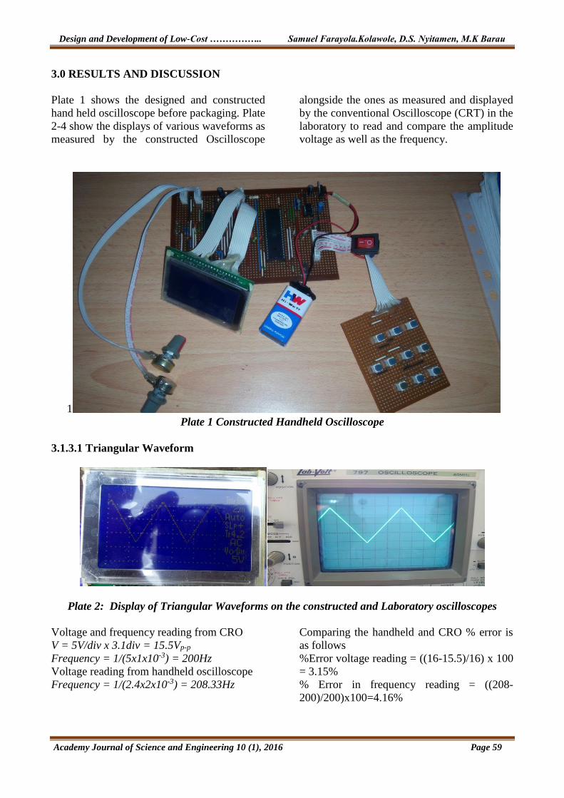
3.0 RESULTS AND DISCUSSION
Plate 1 shows the designed and constructed
hand held oscilloscope before packaging. Plate
2-4 show the displays of various waveforms as
measured by the constructed Oscilloscope
alongside the ones as measured and displayed
by the conventional Oscilloscope (CRT) in the
laboratory to read and compare the amplitude
voltage as well as the frequency.
1
Plate 1 Constructed Handheld Oscilloscope
3.1.3.1 Triangular Waveform
Plate 2: Display of Triangular Waveforms on the constructed and Laboratory oscilloscopes
Voltage and frequency reading from CRO
V = 5V/div x 3.1div = 15.5Vp-p
Frequency = 1/(5x1x10-3) = 200Hz
Voltage reading from handheld oscilloscope
Frequency = 1/(2.4x2x10-3) = 208.33Hz
Comparing the handheld and CRO % error is
as follows
%Error voltage reading = ((16-15.5)/16) x 100
= 3.15%
% Error in frequency reading = ((208-
200)/200)x100=4.16%

Design and Development of Low-Cost …………….. Samuel Farayola.Kolawole, D.S. Nyitamen, M.K Barau
Academy Journal of Science and Engineering 10 (1), 2016 Page 60
3.1.3.2 Square Waveform
Plate 3: Display of Square Waveforms on the constructed and Laboratory oscilloscopes
Voltage and frequency reading from CRO
V = 5V/div x 1.5div = 7.5Vp-p
Frequency = 1/(5.2x20x10-3) = 9.615Hz
Voltage reading from handheld oscilloscope
V=2V/div x 3.7div = 7.4V
Frequency = 1/(2.3x50x10-3) = 8.696Hz
Comparing the handheld and CRO % error is
as follows
%Error voltage reading = ((7.7-7.4)/7.5) x 100
= 1.33%
% Error in frequency reading = ((9.615-
8.696)/9.615)x100=9.56%
3.1.3.3 Sinusoidal Waveform
Plate 4: Display of Sinusoidal Waveforms on the constructed and Laboratory oscilloscopes
Voltage and frequency reading from CRO
V =10V/div x 3.6div =36Vp-p
Voltage reading from handheld oscilloscope
V =10V/div x 3.8div =38Vp-p
Comparing the handheld and CRO % error is
as follows
%Error voltage reading = ((38-36)/36) x 100 =
5.5%

Design and Development of Low-Cost …………….. Samuel Farayola.Kolawole, D.S. Nyitamen, M.K Barau
Academy Journal of Science and Engineering 10 (1), 2016 Page 61
3.1.4 Frequency Measurements
The device constructed device has the
capability of measuring and displaying the
frequency of the measured signal. Some
samples of these signals were measured using
a function generator, and the results obtained
were very good. The accuracy was very high
to the nearest hundred hertz, only at higher
values above 200 kHz that the accuracy tent to
depreciate significantly.
Comparison with the laboratory Frequency
meter was not possible up to the time of filing
this report, as such conclusion cannot be met
as per the discrepancy and reliability of the
system is concerned. The measurement was
only known from the selected or dialled value
on the function generator which could show
other minute details. Other
discrepancies/deviation from the actual values
might be as a result of unstabilised power to
the frequency generating device, excessive
temperature of the environment and etc.
Table 3: Tuned Frequencies and the Displayed Values
Tuned Frequency Value
(Hz)
Reading Displayed by the
Oscilloscope (Hz)
10 10
50 51
150 153
450 447
890 897
1140 1138
12330 12299
40500 40522
100250 100321
150000 150089
200000 199882
550000 549753
870000 871541
1000000 Not stable
5000000 Not stable
15000000 Not stable
4.0 CONCLUSION
The AVR microcontroller based handheld
Oscilloscope has beendesigned ,constructed
and tested. It is well suited for field and
laboratory uses. The program was designed
and written using a modified basic language
for AVR and its compiler called Bascom-avr.
Many waveforms were measured and
reconstructed accurately up to the speed of 20
kHz This limitation could be as a result of the
ADC’s clock speed requirement of 50 kHz to
200 kHz in order to get its maximum
resolution and the conversion of the analog to
digital signal takes 13 ADC clock-cycles to
complete, which further divides the ADC
speed by 13 making the sampling frequency to
be 200/13 kHz (15.38 kHz). By the Shannon-
Nyquist criteria with this sampling rate only
7.69 kHz signal can be fully reconstructed.
“By default, the successive approximation
circuitry of the ADC requires an input clock
frequency between 50kHz and 200 kHz to get
maximum resolution. However, If a lower
resolution than 10 bits is needed, theinput
clock frequency to the ADC can be higher
than 200 kHz to get a higher sample rate.The
ADC module contains a prescaler, which
generates an acceptable ADC clock frequency

Design and Development of Low-Cost …………….. Samuel Farayola.Kolawole, D.S. Nyitamen, M.K Barau
Academy Journal of Science and Engineering 10 (1), 2016 Page 62
from any CPU frequency above 100 kHz”.The
ADC’s pre-scaler was adjusted up to get
higher sampling rate and at the detriment of
the resolution, this made it possible to measure
up to 20 kHz.
The device is handy, that can be physically
justified, and has a low-cost because the total
cost of all the components put together was
only ₦12,410.
REFERENCES
Aditi T; Mukti A (2015) “ARM Based Handy
Portable Oscilloscope Using Graphical
Display” International Journal of
Engineering Research and Applications,
vol.5 , Issue 3, March 2015
Banf Alberta (2011), “Equivalent Sampling
Oscilloscope with External Delay
Embedded System”.IEEE International
Conference onHigh Performance
Computing and Communications
Bhagyashree D.;Amol C (2015) “Effective
Measurement of Frequency and Voltage
Using Android Oscilloscope”
International Journal pof Science,
Technology and Management. Volume
04 issue 01. March 2015
Celma S, Carlosena A (1992) “PC-based
Spectrum Analyser” IEEE Transaction
on Education, vol 35, pp 204-210, Aug
1992
Chandan B, SAikat G, Samrat K (2014) “ A
Low – Cost Based Virtual Oscilloscope”
IEEE Transaction on Education vol 47
no 2 May 2004
Hua F; Hua J (2011) The Research on the
Algorithm of Lattice LCD Drawing
Controlled by PIC (2011), 10th
International Symposium on Distributed
Computing and Applications to
Business, Engineering and Science,
2011
Ishitiak A (2014) “A Low Cost Portable
Oscilloscope Based on Arduino and
GLCD” 3rd International Conference on
Informatics, Electronics and Vision
Janani D; Nivash S (2016) “Low Cost Android
Measuring Embedded Device Using
Input Output Board” International
Journal of Engineering and Innovative
Technology Volume 5 Issue 8 February
2016for an Analog-to-Digital Converter,
IEEE 17th International Mixed Signals,
Sensors and Systems Test Workshop
Shepperd K.L; Zheng Y (2001) “On-chip
Oscilloscopes for Noninvasive Time-
Domain Measurement of waveforms.
“International Conference on Computer
Design (ICCD’01)
Shilpa D, Monika B (2016) “Android Based
Smart Oscilloscope”
International Journal of Innovative
Research in Computer and
Communication Engineering, vol 4 issue
4 April 2016
Yogesh S; Pranjali M (2014) “Graphical LCD
based Digital Oscilloscope using
ATmega32” International Journal of
Electronics, Electrical and
Computational System, Volume 3 Issue
4 June 2014


![Bascom AVR Programming [Basic]](https://img.pdfslide.net/doc/110x75/544a8b55b1af9f0f568b4d6d/bascom-avr-programming-basic.jpg)

