Embed Size (px)
Citation preview
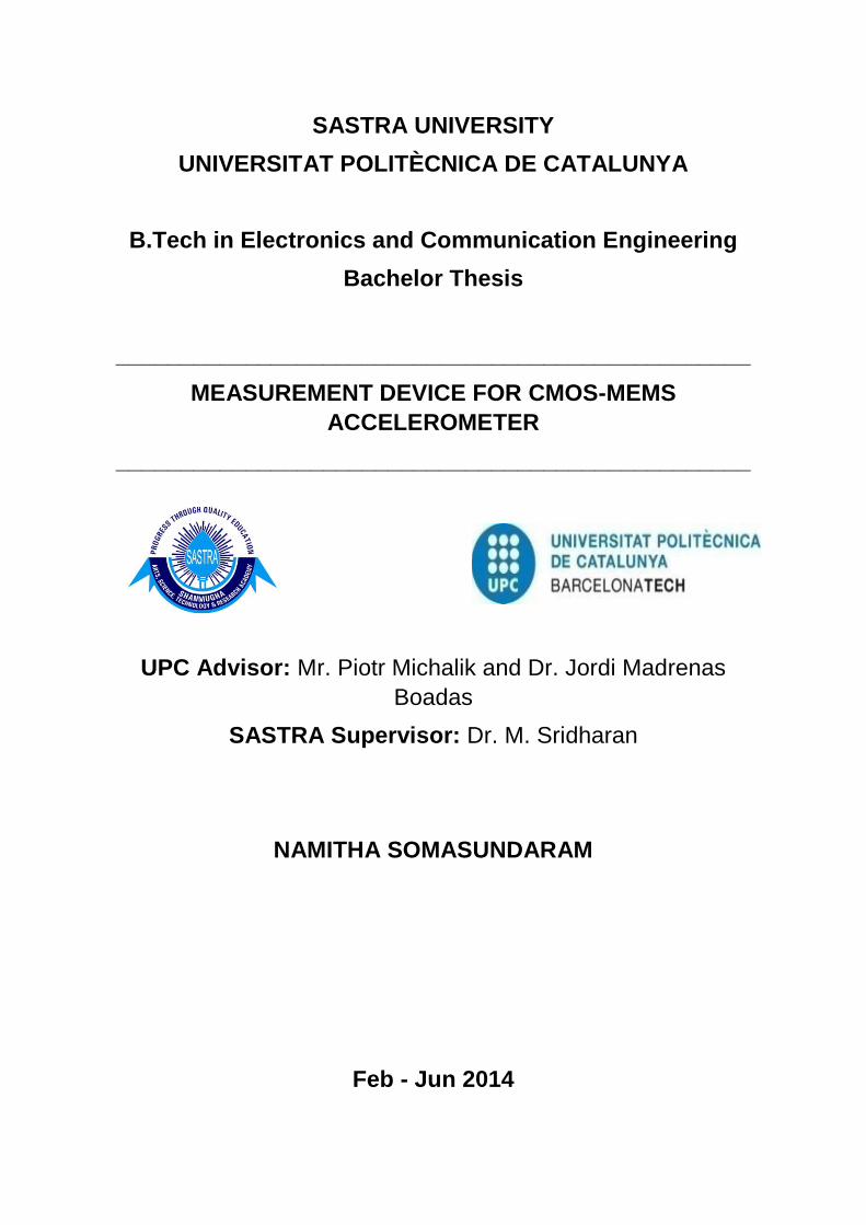
SASTRA UNIVERSITY
UNIVERSITAT POLITÈCNICA DE CATALUNYA
B.Tech in Electronics and Communication Engineering
Bachelor Thesis
_________________________________________________
MEASUREMENT DEVICE FOR CMOS-MEMS
ACCELEROMETER
_________________________________________________
UPC Advisor: Mr. Piotr Michalik and Dr. Jordi Madrenas
Boadas
SASTRA Supervisor: Dr. M. Sridharan
NAMITHA SOMASUNDARAM
Feb - Jun 2014

SASTRA UNIVERSITY
(A University u/s 3 of UGC Act, 1956) Thanjavur – 613 401, Tamil Nadu, India
School of Electrical & Electronics Engineering
BONAFIDE CERTIFICATE
We certify that the project work entitled “MEASUREMENT SYSTEM FOR
CMOS-MEMS ACCELEROMETER” submitted to the Faculty of the Escola
Tècnica d'Enginyeria de Telecomunicació de Barcelona Universitat Politècnica de Catalunya
is the work done by Ms. NAMITHA SOMASUNDARAM in partial fulfillment for
the award of the degree of Bachelor of Technology in Electronics & Communication
Engineering is the work carried out independently under our guidance during the period Feb
– June 2014.
Dr. M. Sridharan Mr. Piotr Michalik and
Internal Guide / Exchange Coordinator Dr. Jordi Madrenas Boadas
SEEE, SASTRA University Advisors, AHA Group
Thanjavur, India Dept of Electronics Engineering,
UPC, Barcelona, Spain
Prof. Jordi Madrenas Boadas
Advanced Hardware Architecture Research Group
Department of Electronic Engineering, ETSETB
CERTIFICATE
This is to certify that the project work titled “MEASUREMENT SYSTEM FOR CMOS-
MEMS ACCELEROMETER” submitted to Faculty of the Escola Tècnica d'Enginyeria de
Telecomunicació de Barcelona Universitat Politècnica de Catalunya by Ms. NAMITHA
SOMASUNDARAM in partial fulfillment of the requirements for the award of the degree of
Bachelor of Technology in Electronics & Communication Engineering is the original and
independent work carried out under my guidance at Advanced Hardware Architecture(AHA)
Research Group, Department of Electronics Engineering, ETSETB, Universitat Politècnica
de Catalunya, Barcelona, Spain, during the period February to June 2014. The contents of this
thesis done by her, in full, or in parts have not been submitted to any institute or University
for the award of any degree or diploma.
Place: (Prof. _______________)
Date: Official Seal

0
DECLARATION
I submit this project work entitled “Measurement System for CMOS-MEMS
Accelerometer” to the Faculty of the Escola Tècnica d'Enginyeria de Telecomunicació
de Barcelona Universitat Politècnica de Catalunya in partial fulfillment of the
requirements for the award of the degree of “Bachelor of Technology” in “Electronics and
Communication Engineering”. I declare that it was carried out independently by me under
the guidance of Dr. Jordi Madrenas Boadas, (External Guide) Associate Professor,
Advanced Hardware Architectures Group, Department of Electronics Engineering,
Universitat Politécnica de Catalunya, Barcelona, Spain and Dr. M. Sridharan (Internal
Guide), School of Electrical & Electronics Engineering, SASTRA University, Thanjavur,
India, during the academic year 2013-2014. This was a record of my own work and to the
best of my knowledge and belief, it contains no material previously published or written
by another person, nor material which has been accepted by any other University or
Institute of higher learning, except where due acknowledgments have made in the text.
- NAMITHA SOMASUNDARAM
Place: Signature:
Date: NAMITHA SOMASUNDARAM

1
ACKNOWLEDGEMENTS
First and foremost, I thank the Almighty, for his blessings throughout my project
work.
I would, at the outset, like to place on record my sincere thanks to Prof. R.
Sethuraman, Vice-Chancellor, and Dr. G. Bhalachandran, Registrar, SASTRA
University for providing me an opportunity to work in such an honored Institute which has
a very good International status. I sincerely thank Dr. S. Vaidhyasubramaniam, Dean-
Planning and Development and Dr. S. Swaminathan, Dean-Sponsored Research for
their support and encouragement.
I thank Dr. B. Viswanathan, Dean-SEEE, Prof. M. Narayanan, Dean-Student
Affairs, Associate Deans and Faculty members of SEEE for their moral support.
I would like to extend my sincere thanks to Dr. Jordi Madrenas Boadas for
accepting me as an exchange student into the Advanced Hardware Architecture group at
Universitat Politècnica de Catalunya, Barcelona. I also thank him for reviewing my thesis
work and giving comments to improve the work.
I extend my heartfelt thanks to Mr. Piotr Michalik, for his support and guidance
all through the work – right from the day of explaining the work till the end. I extend my
warm thanks to Dr. Daniel Fernandez for giving valuable inputs during the design
process of the work and after. I thank Mr. Josep Maria Sánchez Chiva for his help in
testing the chip and for translating my abstract to Spanish and Catalan. I also thank all
my lab mates for making this journey a very good cultural learning experience as well.
My sincere thanks to SASTRA University for providing me an opportunity to carry
out my project work at ETSETB, UPC Barcelona, Spain, through the Semester Abroad
Program and also for providing me Desh-Videsh Scholarship. Very special thanks to my
Internal guide/Exchange Coordinator, Prof. M. Sridharan, Department of Electronics &
Communication Engineering, SASTRA University for his constant support for my project
work / administrative procedures and for initiating and strengthening the link between
SASTRA and ETSETB, UPC Barcelona, Spain.
I would like to convey my hearty thanks to my Family members and my Friends,
for their moral support in completion of this project successfully.
Namitha Somasundaram

2
Abstract
This project reports the process of development of the Printed Circuit Board (PCB) - Zephyr for the experimental CMOS MEMS accelerometer testchip, Bailed II. The problem of capacitance mismatch at the input bridge is solved through a simple and innovative arrangement of resistors, jumpers and capacitors on the PCB. A filter is designed with the inductor capacitor pair to filter noise from the DC source. An amplifier with a gain of 10 is designed to amplify the output signals of the Bailed II IC. A cascaded amplifier topology is used to achieve the required gain. The PCB is tested to be functional and a few measurements were done with the chip. Furthermore, a multiple feedback (MFB) topology filter is designed for a second PCB which hosts the circuits (namely, band gap reference voltage IC, filter and Analog-to-Digital Converter) for further conditioning of signals before they are given to the FPGA. This second PCB is planned to be used for a new CMOS-MEMS testchip that has been recently designed.
Index Terms - Accelerometer, CMOS-MEMS, capacitive accelerometer, capacitance mismatch, Printed Circuit Board, PCB, cascaded amplifier, Multi Feedback topology filter

3
Resum
Aquest projecte mostra el procés de desenvolupament de la placa de circuit imprès (PCB) - Zephyr pel xip de test de l'acceleròmetre CMOS-MEMS Bailed II. El problema del desajust de la capacitat al pont d'entrada s'ha resolt mitjançant una xarxa de resistències, jumpers i condensadors simple i innovadora implementada en el circuit imprès. S'ha dissenyat un filtre amb un parell condensador-bobina per eliminar el soroll provinent de la font de DC. S'ha dissenyat un amplificador amb un guany de 10 per amplificar els senyals de sortida del circuit integrat Bailed II. S'ha utilitzat una topologia d'amplificador en cascada per aconseguir el guany requerit. S'ha comprovat el correcte funcionament de la PCB i s'han realitzat algunes mesures amb el xip. A més, s'ha dissenyat un filtre amb topologia de realimentació múltiple (MFB) per a una segona PCB que conté els circuits (un circuit integrat de referència de tensió tipus bandgap, un filtre i un circuit convertidor d'analògic a digital) per a un millor condicionament dels senyals abans de ser introduïts en una FPGA. Es preveu que aquesta segona PCB pugui ser utilitzada per a un nou xip de test CMOS-MEMS que ha estat dissenyat recentment.
Índex de Termes - Acceleròmetre , CMOS - MEMS, acceleròmetre capacitiu, desajust de capacitat, Placa de Circuit Imprès, PCB, amplificador en cascada, filtre amb topologia de realimentació múltiple

4
Resumen
Este proyecto muestra el proceso de desarrollo de la placa de circuito impreso (PCB) - Zephyr para el chip de test del acelerómetro CMOS-MEMS Bailed II. El problema del desajuste de la capacidad en el puente de entrada se ha resuelto mediante una red de resistencias, jumpers y condensadores simple e innovadora implementada en la placa de circuito impreso. Se ha diseñado un filtro con un par condensador-bobina para filtrar los ruidos de la fuente de DC. Se ha diseñado un amplificador con una ganancia de 10 para amplificar las señales de salida del circuito integrado Bailed II. Se ha empleado una topología de amplificador en cascada para obtener la ganancia requerida. Se ha testeado el correcto funcionamiento de la PCB y se han realizado algunas medidas con el chip. Además, se ha diseñado un filtro con una topología de realimentación múltiple (MFB) para una segunda PCB dónde se conectaran los circuitos (un circuito integrado de tensión de referencia tipo bandgap, un filtro y un convertidor de analógico a digital) para un mejor acondicionamiento de la señal antes de ser introducido en una FPGA. Se prevé que esta segunda PCB pueda ser utilizada para un nuevo chip de test CMOS-MEMS que ha sido diseñado recientemente.
Índice de Términos - Acelerómetro, CMOS-MEMS, acelerómetro capacitivo, desajuste de capacidad, Placa de Circuito Impreso, PCB, amplificador en cascada, filtro con topología de realimentación múltiple

5
Revision history and approval record
Revision Date Purpose
0 13/05/2014 Document creation
1 28/05/2014 Document revision
2 03/06/2014 Document revision
3 04/06/2014 Document approval
DOCUMENT DISTRIBUTION LIST
Name e-mail
Namitha Somasundaram [email protected]
Prof. Jordi Madrenas Boadas [email protected]
Mr. Piotr Michalik [email protected]
Prof. M. Sridharan [email protected]
Written by: Reviewed and approved by:
Date 16/05/2014 Date 04/06/2014
Name Namitha Somasundaram Name Dr. Jordi Madrenas Boadas
Position Project Author Position Project Supervisor

Table of contents
The table of contents must be detailed. Each chapter and main section in the thesis must be
listed in the “Table of Contents” and each must be given a page number for the location of a
particular text.
Acknowledgements………………………………………………………………………………1
Abstract............................................................................................................................ 2
Resum ............................................................................................................................. 3
Resumen ......................................................................................................................... 4
Revision history and approval record ............................................................................... 5
Table of contents ............................................................................................................. 6
List of Figures .................................................................................................................. 6
List of Tables: .................................................................................................................. 3
1. Introduction ............................................................................................................. 13
1.1. Motive of the project ......................................................................................... 13
1.2. State of Art ........................................................................................................ 14
1.3 Software Slection……………………………………………………………………17
1.4 Conclusion…………………………………………………………………………...18
2. Modules of Design .................................................................................................. 19
2.1. Voltage Regulator ............................................................................................ 20
2.2. Voltages given to the chip ................................................................................ 22
2.3. Noise Removal Circuit - Filter .......................................................................... 32
2.4. Amplifier ........................................................................................................... 35
2.5. Points to remember when doing the schematic ................................................ 37
2.6. Conclusion ....................................................................................................... 37
3. PCB Design ............................................................................................................ 38
3.1. Schematic to PCB Conversion ......................................................................... 38
3.2. PCB Design Procedure .................................................................................... 39
3.3. Placement of Components ............................................................................... 41
3.4. Routing and Afterwork ..................................................................................... 47
3.5. Conclusion ....................................................................................................... 53
4. Measurements ........................................................................................................ 54
4.1. PCB Manufacturing and Soldering ................................................................... 54
4.2. Initial Setup ...................................................................................................... 56

4.3. Easily overlooked points .................................................................................. 57
4.4. Testing processes in detail ............................................................................... 57
4.5. Regarding Bandwidth ....................................................................................... 61
4.6. Some improvements that could have been done ............................................. 62
4.7. Testing the chip ............................................................................................... 62
4.8. Further work with this chip ............................................................................... 63
4.9. Conclusion ....................................................................................................... 63
5. PCB2 ........................................................................................................................ 64
5.1. Introduction ...................................................................................................... 64
5.2. Overview of the work ....................................................................................... 64
2.6. Ongoing work ................................................................................................... 66
2.6. Conclusion ....................................................................................................... 66
6. Conclusion .............................................................................................................. 67
7. Bibliography: ........................................................................................................... 68
Appendices .................................................................................................................... 69

List of Figures:
S.No Figure
Number
Figure Name Page
No.
1 1.1 Arrangement of the parallel plates 14
2 1.2 Rough approximation of Bailed II IC 15
3 1.3 A released MEMS layer in Bailed II IC 16
4 1.4 Releasing the MEMS 17
5 2.1 Modules in PCB 19
6 2.2 Standard setup for using LM317BTG 21
7 2.3 Voltage Regulator 22
8 2.4 Driving voltages 23
9 2.5 Control voltages setup 24
10 2.6 Relation between VGS and ID 24
11 2.7 VB_I voltage 25
12 2.8 Circuit for producing 50µA 25
13 2.9 Circuit for producing 150µA 25
14 2.10 Vbias voltage and the chip 26
15 2.11 Graph between VGS and ID 26
16 2.12 Vbias of 500mV 26
17 2.13 Vbias of 720mV 26
18 2.14 Rough approximation of the chip 27
19 2.15 Carrier signal and subsequent filtering 28
20 2.16 Setting the DC value 29
21 2.17 Setting the DC point at 1V 30
22 2.18 Alternate DC supply arrangement 30
23 2.19 Arrangement for inputs inn and inp 31

24 2.20 Jumper J11 and J10 used 32
25 2.21 Jumper J9 and J12 used 32
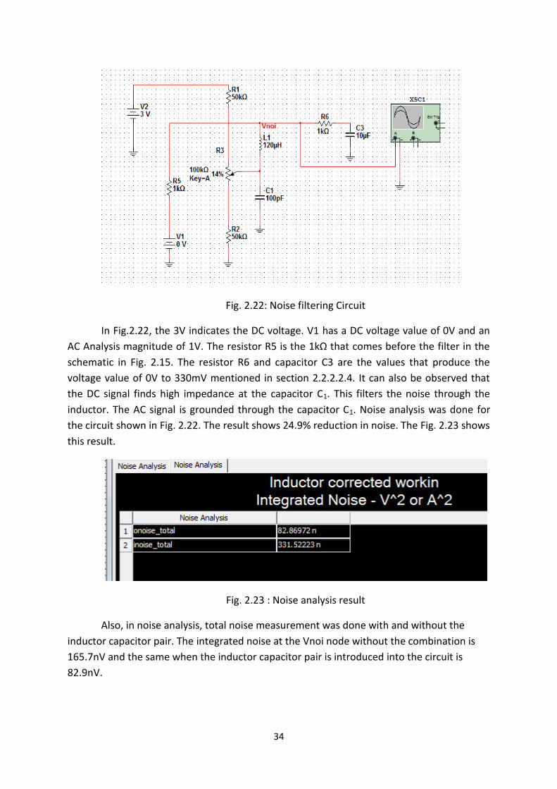
26 2.22 Noise filtering Circuit 34
27 2.23 Noise analysis result 34
28 2.24 Noise removal circuit 35
29 2.25 Cascaded stages of amplifier 35
30 2.26 Multisim circuit with the net names 36
31 2.27 Graph showing the transient analysis response 37
32 3.1 xgsch2pcb Graphical User Interface 39
33 3.2 PCB with the components after they are dispersed 39
34 3.3 The result of auto-placement of all components 42
35 3.4 First arrangement of components 43
36 3.5 Proper arrangement of components at the output 44
37 3.6 Resolving the component placement for signals inn and inp 45
38 3.7 Final design with proper aesthetic sense 46
39 3.8 Peelables 47
40 3.9 Ground connections 48
41 3.10 Footprint mismatch 49
42 3.11 Missing parts in top silk 49
43 3.12 Correct version of top silk 49
44 3.13 PCB with Gnd planes and the power line routing 50
45 3.14 Unrouted rat 50
46 3.15 PCB which is fully routed 51
47 3.16 The final PCB design 52
48 3.17 PCB passes the DRC check 52
49 4.1 Component side of Zephyr 54
50 4.2 Solder side of Zephyr 55
51 4.3 Soldering in progress 55
52 4.4 Zephyr used in measurements without the chip 56
53 4.5 Jumper J3 and J4 usage 57
53 4.6 Single input single output op amp 58
54 4.7 Voltage divider that was formed 59
55 4.8 Output with 2kΩ load 59
56 4.9 Output with 1kΩ load 59
57 4.10 Output waveform at 1MHz 60
58 4.11 Schematic of PCB 60
59 4.12 Gain for 3MHz signal 61
60 4.13 Zephyr with Bailed II IC 62
61 5.1 Rough approximation of PCB2 64
62 5.2 MFB low pass filter for 1.4MHz cut off frequency 65

List of Tables
S.No Table
Number
Table Name Page
No.
1 1.1 Details of the MEMS sensor used in Bailed II 17
2 2.1 Comparison of different voltage regulators 20
3 3.1 Values for DRC check 40
4 3.2 The width of different signal lines 41
5 4.1 Table showing the voltages after the chip was tested initially 63

5
Revision history and approval record
Revision Date Purpose
0 13/05/2014 Document creation
1 28/05/2014 Document revision
2 03/06/2014 Document revision
3 04/06/2014 Document approval
DOCUMENT DISTRIBUTION LIST
Name e-mail
Namitha Somasundaram [email protected]
Prof. Jordi Madrenas Boadas [email protected]
Mr. Piotr Michalik [email protected]
Prof. M. Sridharan [email protected]
Written by: Reviewed and approved by:
Date 16/05/2014 Date 04/06/2014
Name Namitha Somasundaram Name Dr. Jordi Madrenas Boadas
Position Project Author Position Project Supervisor

6
Table of contents
The table of contents must be detailed. Each chapter and main section in the thesis must be
listed in the “Table of Contents” and each must be given a page number for the location of a
particular text.
Acknowledgements………………………………………………………………………………1
Abstract............................................................................................................................ 2
Resum ............................................................................................................................. 3
Resumen ......................................................................................................................... 4
Revision history and approval record ............................................................................... 5
Table of contents ............................................................................................................. 6
List of Figures .................................................................................................................. 8
List of Tables: ................................................................................................................ 11
1. Introduction ............................................................................................................. 13
1.1. Motive of the project ......................................................................................... 13
1.2. State of Art ........................................................................................................ 14
1.3 Software Slection……………………………………………………………………17
1.4 Conclusion…………………………………………………………………………...18
2. Modules of Design .................................................................................................. 19
2.1. Voltage Regulator ............................................................................................ 20
2.2. Voltages given to the chip ................................................................................ 22
2.3. Noise Removal Circuit - Filter .......................................................................... 32
2.4. Amplifier ........................................................................................................... 35
2.5. Points to remember when doing the schematic ................................................ 37
2.6. Conclusion ....................................................................................................... 37
3. PCB Design ............................................................................................................ 38
3.1. Schematic to PCB Conversion ......................................................................... 38
3.2. PCB Design Procedure .................................................................................... 39
3.3. Placement of Components ............................................................................... 41
3.4. Routing and Afterwork ..................................................................................... 47
3.5. Conclusion ....................................................................................................... 53
4. Measurements ........................................................................................................ 54
4.1. PCB Manufacturing and Soldering ................................................................... 54
4.2. Initial Setup ...................................................................................................... 56

7
4.3. Easily overlooked points .................................................................................. 57
4.4. Testing processes in detail ............................................................................... 57
4.5. Regarding Bandwidth ....................................................................................... 61
4.6. Some improvements that could have been done ............................................. 62
4.7. Testing the chip ............................................................................................... 62
4.8. Further work with this chip ............................................................................... 63
4.9. Conclusion ....................................................................................................... 63
5. PCB2 ........................................................................................................................ 64
5.1. Introduction ...................................................................................................... 64
5.2. Overview of the work ....................................................................................... 64
2.6. Ongoing work ................................................................................................... 66
2.6. Conclusion ....................................................................................................... 66
6. Conclusion .............................................................................................................. 67
7. Bibliography: ........................................................................................................... 68
Appendices .................................................................................................................... 69

8
List of Figures:
S.No Figure
Number
Figure Name Page
No.
1 1.1 Arrangement of the parallel plates 14
2 1.2 Rough approximation of Bailed II IC 15
3 1.3 A released MEMS layer in Bailed II IC 16
4 1.4 Releasing the MEMS 17
5 2.1 Modules in PCB 19
6 2.2 Standard setup for using LM317BTG 21
7 2.3 Voltage Regulator 22
8 2.4 Driving voltages 23
9 2.5 Control voltages setup 24
10 2.6 Relation between VGS and ID 24
11 2.7 VB_I voltage 25
12 2.8 Circuit for producing 50µA 25
13 2.9 Circuit for producing 150µA 25
14 2.10 Vbias voltage and the chip 26
15 2.11 Graph between VGS and ID 26
16 2.12 Vbias of 500mV 26
17 2.13 Vbias of 720mV 26
18 2.14 Rough approximation of the chip 27
19 2.15 Carrier signal and subsequent filtering 28
20 2.16 Setting the DC value 29
21 2.17 Setting the DC point at 1V 30
22 2.18 Alternate DC supply arrangement 30
23 2.19 Arrangement for inputs inn and inp 31

9
24 2.20 Jumper J11 and J10 used 32
25 2.21 Jumper J9 and J12 used 32
26 2.22 Noise filtering Circuit 34
27 2.23 Noise analysis result 34
28 2.24 Noise removal circuit 35
29 2.25 Cascaded stages of amplifier 35
30 2.26 Multisim circuit with the net names 36
31 2.27 Graph showing the transient analysis response 37
32 3.1 xgsch2pcb Graphical User Interface 39
33 3.2 PCB with the components after they are dispersed 39
34 3.3 The result of auto-placement of all components 42
35 3.4 First arrangement of components 43
36 3.5 Proper arrangement of components at the output 44
37 3.6 Resolving the component placement for signals inn and inp 45
38 3.7 Final design with proper aesthetic sense 46
39 3.8 Peelables 47
40 3.9 Ground connections 48
41 3.10 Footprint mismatch 49
42 3.11 Missing parts in top silk 49
43 3.12 Correct version of top silk 49
44 3.13 PCB with Gnd planes and the power line routing 50
45 3.14 Unrouted rat 50
46 3.15 PCB which is fully routed 51
47 3.16 The final PCB design 52
48 3.17 PCB passes the DRC check 52
49 4.1 Component side of Zephyr 54

10
50 4.2 Solder side of Zephyr 55
51 4.3 Soldering in progress 55
52 4.4 Zephyr used in measurements without the chip 56
53 4.5 Jumper J3 and J4 usage 57
53 4.6 Single input single output op amp 58
54 4.7 Voltage divider that was formed 59
55 4.8 Output with 2kΩ load 59
56 4.9 Output with 1kΩ load 59
57 4.10 Output waveform at 1MHz 60
58 4.11 Schematic of PCB 60
59 4.12 Gain for 3MHz signal 61
60 4.13 Zephyr with Bailed II IC 62
61 5.1 Rough approximation of PCB2 64
62 5.2 MFB low pass filter for 1.4MHz cut off frequency 65

11
List of Tables
S.No Table
Number
Table Name Page
No.
1 1.1 Details of the MEMS sensor used in Bailed II 17
2 2.1 Comparison of different voltage regulators 20
3 3.1 Values for DRC check 40
4 3.2 The width of different signal lines 41
5 4.1 Table showing the voltages after the chip was tested initially 63

12
THIS PAGE IS LEFT BLANK INTENTIONALLY

13
Chapter 1 – Introduction
1.1 – Motive of the project 1.2 – State of Art 1.2.1 – Functioning of an accelerometer 1.2.2 - Overview of the chip 1.2.2.1 – Electronics part 1.2.2.2 – MEMS part 1.2.3 – Moving from Standard MEMS to CMOS MEMS 1.3 – Software Selection 1.4 - Conclusion __________________________________________________________________________________
It is not the strongest of the species that survive, nor the most intelligent, but the one most responsive to change.
- Charles Darwin
An accelerometer is a device that measures the change in velocity. Going by Darwin's
words, they cannot be eliminated from the face of the Earth but can only be modified to be more useful! This by itself is a measure of the important role accelerometers play in our lives.
Do people fancy drawing in air and making it appear on the screen of their iPhone? This is done with an application! Air Paint is the word! The working of this application mainly depends on accelerometers.
Accelerometers are of utmost importance in automobile airbag crash sensor. This sensor looks out for a sudden reduction in velocity. When this occurs, the airbag has to activate. There can also be situations where the potholes can cause a lot of shock. During those times the accelerometer should not trigger the airbag.
Another application is to determine the aging of equipments. The vibrations produced by an equipment increases with aging. These vibrations can be sensed by the accelerometers that are attached to the bearings. This helps to extend the service life of the equipment without risking sudden failure of the equipment.
Seeing the interesting applications of the accelerometers, the further sections
explain about the functioning of the accelerometer.
1.1 Motive of the project
Bailed II is a novel CMOS-MEMS accelerometer testchip that was designed at the
Department of Electronics Engineering of the UPC (AHA group). The IC was manufactured at
the IHP foundry, which provided engineering samples to be checked for its proper
14
functioning. This required a Printed Circuit Board (PCB) for the measurements purpose.
Thereby a PCB was designed to check its functioning. The PCB design requires the
development of schematic, conversion to PCB and, placement and routing of components in
PCB. The measurements were finally made to verify the functionality.
1.2 State of Art
1.2.1. Functioning of an accelerometer
An accelerometer is a sensor that measures acceleration. There are many types of accelerometers. They include:
Accelerometers that use piezoelectric effect Accelerometers using changes in capacitance Accelerometers using piezoresistive effect Accelerometers using hot air bubbles Accelerometers using light
Fig.1.1 shows a rough approximation of the arrangement for accelerometers that
use change in capacitance.
Fig.1.1: Arrangement of the parallel plates [1]
The working principle[2] of accelerometer is that it has a mass suspended and a
force is applied on that. This mass is called the proof mass. In the case of capacitance accelerometers, when one of the two plates moves, because of a change in velocity, the capacitance value differs. In the case of a differential capacitor accelerometer, the output voltage is found to be linear with the distance of separation between the plates of the capacitor. The output will be zero if there is no change in the capacitance value. The output voltage produced because of the displacement needs to be amplified.
In an oscillator, the fundamental relation between acceleration (a) and displacement
(x) is given as shown in eq. 1.1 [3],
15
------------------ (1.1)
where ω0 is the angular frequency. It can be seen that, higher the frequency, lesser will be the displacement. So to measure small acceleration values, higher sensitivity is needed. Higher sensitivity means lower oscillation frequency.
1.2.2 Overview of the Bailed II testchip
Bailed II is a CMOS MEMS accelerometer. The Micro Electro Mechanical Systems (MEMS) integrate electro-mechanical elements all patterned on a silicon substrate with standard micro fabrication techniques. Feature dimensions are of the order of 1 μm. Integration of the MEMS device with the required conditioning and processing electronics becomes increasingly important for compactness and performance reasons [4-7].
This work uses a CMOS-MEMS accelerometer that integrates the conditioning electronics. It has been designed to work with changes in the capacitance value, thus it is called capacitive accelerometer or vibration sensor. The structure of this accelerometer consists of two parallel plate capacitors which work with differential inputs. Of the two plates that form a capacitor, one plate is movable and the other is a fixed one. The movable plate is the MEMS device. It is a single axis accelerometer which senses change in velocity in the z-axis. After being manufactured with a standard CMOS process, the movable plate is made by post-CMOS micromachining. Therefore the single chip can be thought of to be made of two parts - the electronics part and the MEMS part.
1.2.2.1 Electronics part
A rough approximation of is the basic cell inside the chip is shown in Fig. 1.2.
Fig. 1.2: Rough approximation of Bailed II IC
16
The capacitor C1 has released MEMS as it moving plate of the capacitor. The capacitor C2 is unreleased MEMS. If there is a change in the testchip velocity, acceleration is produced and the MEMS released plate moves and thereby the capacitance value changes. The change in capacitance is converted to a voltage using equations (1.2) and (1.3).
------------------ (1.2)
------------------ (1.3)
This voltage is then amplified through an open-loop amplifier. The high resistance
that is available inside the chip is for adjusting the DC bias value. This concludes the electronics part present in Bailed II IC.
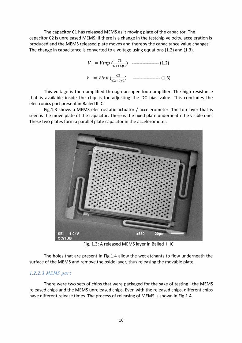
Fig.1.3 shows a MEMS electrostatic actuator / accelerometer. The top layer that is seen is the move plate of the capacitor. There is the fixed plate underneath the visible one. These two plates form a parallel plate capacitor in the accelerometer.
Fig. 1.3: A released MEMS layer in Bailed II IC
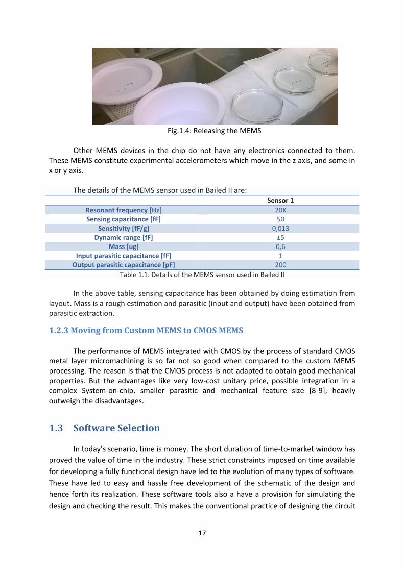
The holes that are present in Fig.1.4 allow the wet etchants to flow underneath the
surface of the MEMS and remove the oxide layer, thus releasing the movable plate.
1.2.2.3 MEMS part
There were two sets of chips that were packaged for the sake of testing –the MEMS released chips and the MEMS unreleased chips. Even with the released chips, different chips have different release times. The process of releasing of MEMS is shown in Fig.1.4.
17
Fig.1.4: Releasing the MEMS
Other MEMS devices in the chip do not have any electronics connected to them.
These MEMS constitute experimental accelerometers which move in the z axis, and some in x or y axis.
The details of the MEMS sensor used in Bailed II are:
Sensor 1
Resonant frequency [Hz] 20K Sensing capacitance [fF] 50
Sensitivity [fF/g] 0,013 Dynamic range [fF] ±5
Mass [ug] 0,6 Input parasitic capacitance [fF] 1
Output parasitic capacitance [pF] 200
Table 1.1: Details of the MEMS sensor used in Bailed II
In the above table, sensing capacitance has been obtained by doing estimation from layout. Mass is a rough estimation and parasitic (input and output) have been obtained from parasitic extraction.
1.2.3 Moving from Custom MEMS to CMOS MEMS
The performance of MEMS integrated with CMOS by the process of standard CMOS metal layer micromachining is so far not so good when compared to the custom MEMS processing. The reason is that the CMOS process is not adapted to obtain good mechanical properties. But the advantages like very low-cost unitary price, possible integration in a complex System-on-chip, smaller parasitic and mechanical feature size [8-9], heavily outweigh the disadvantages.
1.3 Software Selection
In today’s scenario, time is money. The short duration of time-to-market window has
proved the value of time in the industry. These strict constraints imposed on time available
for developing a fully functional design have led to the evolution of many types of software.
These have led to easy and hassle free development of the schematic of the design and
hence forth its realization. These software tools also a have a provision for simulating the
design and checking the result. This makes the conventional practice of designing the circuit
18
on the breadboard and checking the functionality of the design as on outdated one. Given
below are some of the tools available in the market for the same [10].
Eagle
Protel
gEDA
Allegro
KiCAD
PadsPCB
ORCAD
PowerPCB
The selected software used for developing Zephyr, the PCB for Bailed II is gEDA [11].
This open source software runs on Linux and has provisions for using electrical circuit
design, schematic capture, simulation, prototyping, and production. Currently, there is
support for Windows PC. But there are many glitches in the execution part. So gEDA was
used in Linux platform for this work.
Using gEDA has many advantages. It has produced tools which are used for electrical
circuit design, schematic capture, simulation, prototyping, and production. Currently, the
gEDA project offers a mature suite of free software applications for electronics design;
including schematic capture, attribute management, bill of materials (BOM) generation,
netlisting into over 20 netlist formats, analog and digital simulation, and printed circuit
board (PCB) design layout [12].
1.4 Conclusion
This chapter has given a short introduction to the application of accelerometers. It
has then described the motive behind this work. Later, the general functioning of the
accelerometer is described. This chapter then proceeds to explain briefly about the chip.
Finally it concludes with the software that is used for the design of the schematic of the PCB
and points out reasons for using the same.
19
Chapter 2 – Modules of Design
2.1 Voltage Regulator 2.2 Voltages given to the chip 2.2.1 Driving Voltages
2.2.1.1 Control Voltages – Vctr1 and Vctr2 2.2.1.2 VB_I
2.2.1.3 Vbias 2.2.2 Input Voltages
2.2.2.1 Background about the chip 2.2.2.2 Inp and Inn
2.2.2.2.1 Carrier Signal 2.2.2.2.2 Setting the DC Point 2.2.2.2.3 Filtering the noise 2.2.2.2.4 Arrangement of jumpers, resistors and capacitors
2.3 Noise Removal Circuit - Filter 2.4 Amplifier 2.5 Points to remember when doing the schematic 2.6 Conclusion ___________________________________________________________________________
All good work is done the way ants do things, little by little.
-Lafcadio Hearn
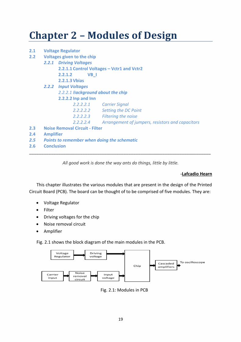
This chapter illustrates the various modules that are present in the design of the Printed
Circuit Board (PCB). The board can be thought of to be comprised of five modules. They are:
Voltage Regulator
Filter
Driving voltages for the chip
Noise removal circuit
Amplifier
Fig. 2.1 shows the block diagram of the main modules in the PCB.
Fig. 2.1: Modules in PCB

20
2.1 Voltage Regulator
The power supply to the board is of utmost importance. A constant power supply is
required for proper functioning of the many stages involved in the design. A voltage
regulator is a device that maintains a constant output voltage irrespective of the changes in
the input voltage and load conditions. A voltage regulator is thereby used to achieve a
constant voltage level.
The following parameters were considered when selecting the suitable voltage
regulator:
Input Voltage
Output Voltage
Output current
Root Mean Square (RMS) noise
Number of terminals - Lesser number of terminals mean easier to solder the
component
The potential candidates for filling the bill of a suitable voltage regulator are tabulated in
Table 2.1.
Device Name
Input Voltage :
Vin (in V)
Output Voltage :
Vo (in V)
Output Current
(in A)
RMS Noise
Number of Terminals
Comments
LT1763[13] 1.8 to 20 3 possible 500m 20μVRMS (10Hz to 100kHz)
8-Lead SO and 12-Lead
(4mm × 3mm) DFN Packages
Difficult to solder
LT1761[14] 1.8 to 20 3 possible
100m 20μVRMS (10Hz to 100kHz)
5-Lead TSOT-23 Package
Less output current
LM4132[15] 2.2 to 5.5
3 possible 20m
170/ 190/ 240/ 285/ 310/ 350 μVpp at 0.1-
10Hz
5 – Lead SOT 23
package
Less output current
LM 317BTG[16]
Vo - Vin = 5
Adjustable type
2.2 0.003 % of Vo Standard 3 lead
transistor package
Good level of output current
and easy to solder
Table 2.1: Comparison of different voltage regulators
21
So from the above Table 2.1, it can be seen that LM317BTG is the best suited for the
design of the required voltage regulator.
The standard application using LM317 is as follows:
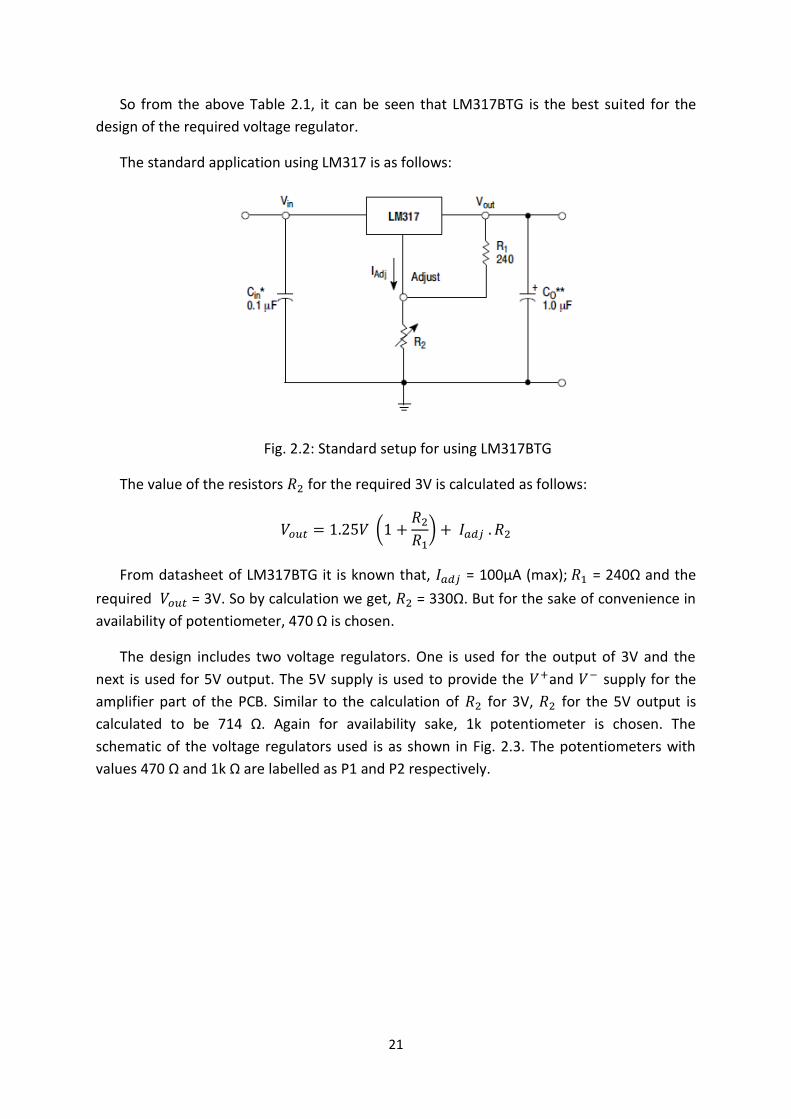
Fig. 2.2: Standard setup for using LM317BTG
The value of the resistors for the required 3V is calculated as follows:
From datasheet of LM317BTG it is known that, = 100µA (max); = 240Ω and the
required = 3V. So by calculation we get, = 330Ω. But for the sake of convenience in
availability of potentiometer, 470 Ω is chosen.
The design includes two voltage regulators. One is used for the output of 3V and the
next is used for 5V output. The 5V supply is used to provide the and supply for the
amplifier part of the PCB. Similar to the calculation of for 3V, for the 5V output is
calculated to be 714 Ω. Again for availability sake, 1k potentiometer is chosen. The
schematic of the voltage regulators used is as shown in Fig. 2.3. The potentiometers with
values 470 Ω and 1k Ω are labelled as P1 and P2 respectively.
22
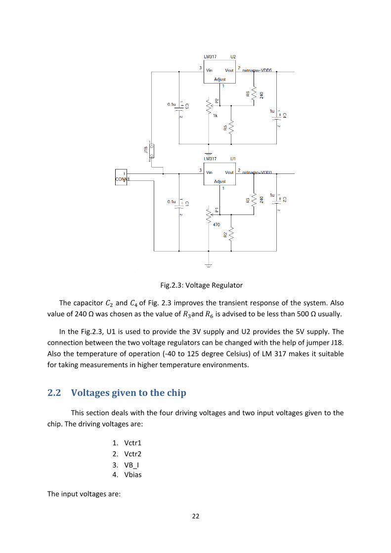
Fig.2.3: Voltage Regulator
The capacitor and of Fig. 2.3 improves the transient response of the system. Also
value of 240 Ω was chosen as the value of and is advised to be less than 500 Ω usually.
In the Fig.2.3, U1 is used to provide the 3V supply and U2 provides the 5V supply. The
connection between the two voltage regulators can be changed with the help of jumper J18.
Also the temperature of operation (-40 to 125 degree Celsius) of LM 317 makes it suitable
for taking measurements in higher temperature environments.
2.2 Voltages given to the chip
This section deals with the four driving voltages and two input voltages given to the
chip. The driving voltages are:
1. Vctr1
2. Vctr2
3. VB_I 4. Vbias
The input voltages are:
23
1. Inp 2. Inn
2.2.1 Driving Voltages
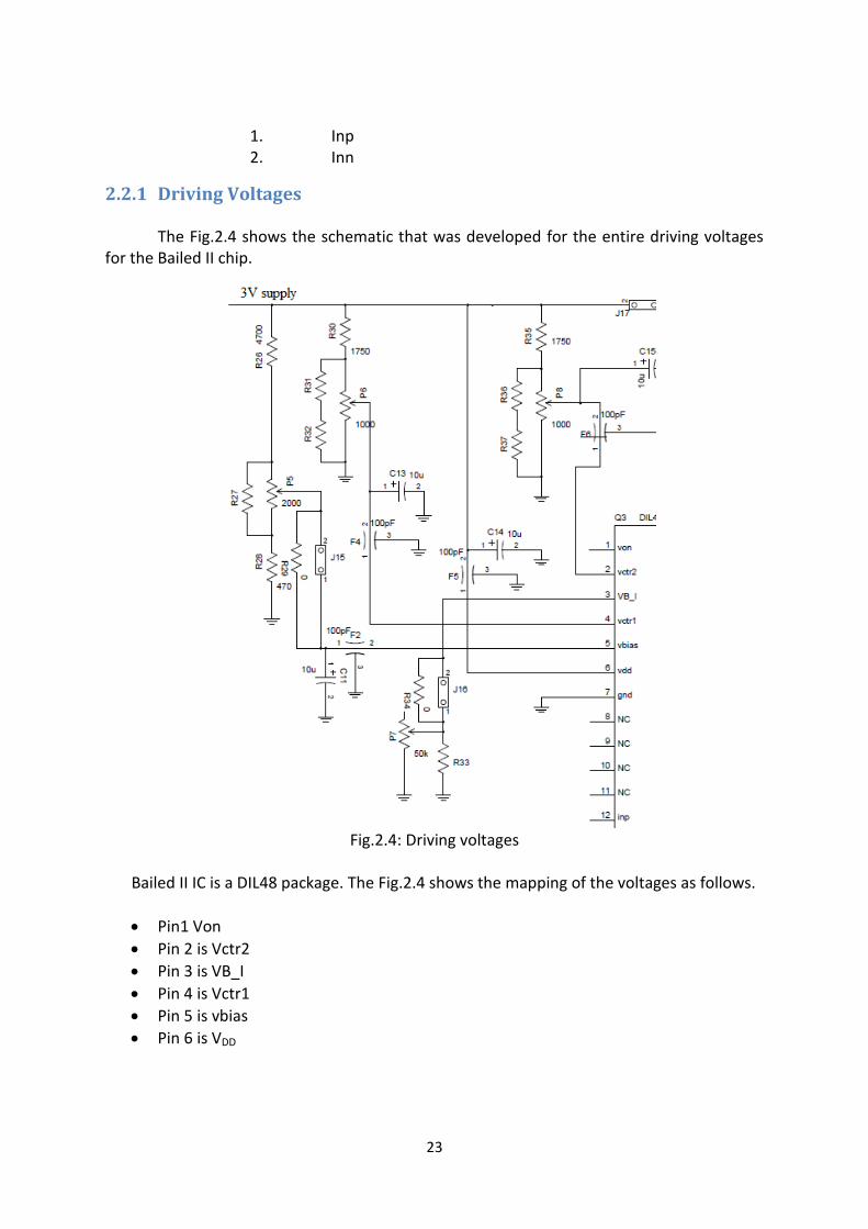
The Fig.2.4 shows the schematic that was developed for the entire driving voltages for the Bailed II chip.
Fig.2.4: Driving voltages
Bailed II IC is a DIL48 package. The Fig.2.4 shows the mapping of the voltages as follows.
Pin1 Von
Pin 2 is Vctr2
Pin 3 is VB_I
Pin 4 is Vctr1
Pin 5 is vbias
Pin 6 is VDD
24
2.2.1.1 Control Voltages – Vctr1 and Vctr2
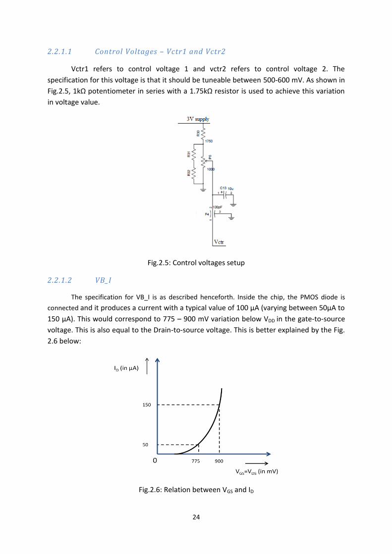
Vctr1 refers to control voltage 1 and vctr2 refers to control voltage 2. The
specification for this voltage is that it should be tuneable between 500-600 mV. As shown in
Fig.2.5, 1kΩ potentiometer in series with a 1.75kΩ resistor is used to achieve this variation
in voltage value.
Fig.2.5: Control voltages setup
2.2.1.2 VB_I
The specification for VB_I is as described henceforth. Inside the chip, the PMOS diode is
connected and it produces a current with a typical value of 100 µA (varying between 50µA to
150 µA). This would correspond to 775 – 900 mV variation below VDD in the gate-to-source
voltage. This is also equal to the Drain-to-source voltage. This is better explained by the Fig.
2.6 below:
Fig.2.6: Relation between VGS and ID
25
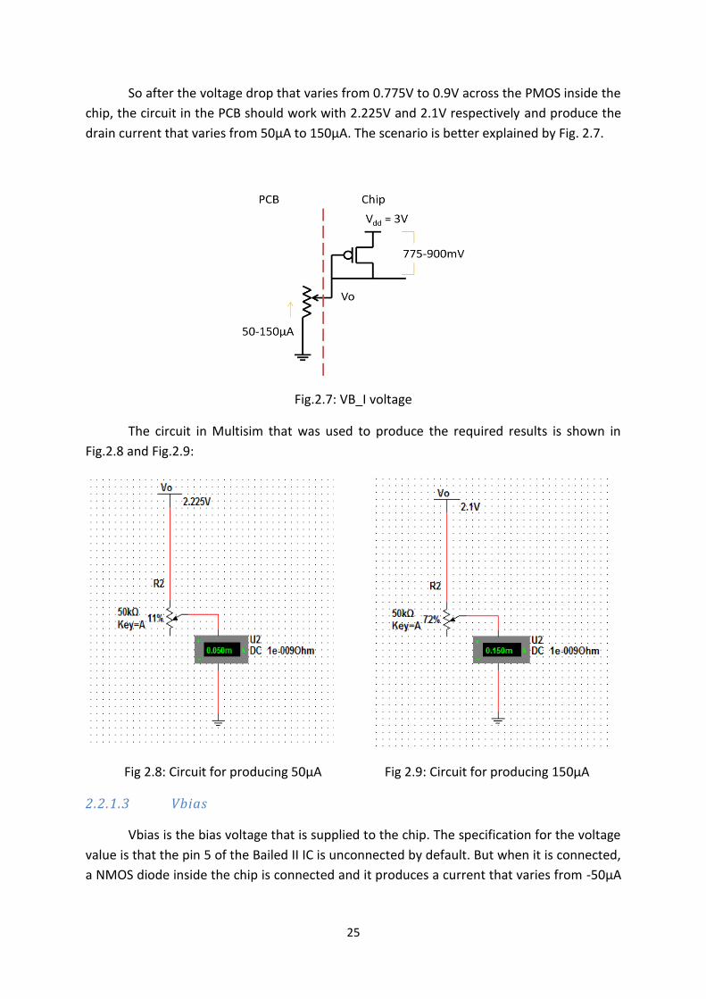
So after the voltage drop that varies from 0.775V to 0.9V across the PMOS inside the
chip, the circuit in the PCB should work with 2.225V and 2.1V respectively and produce the
drain current that varies from 50µA to 150µA. The scenario is better explained by Fig. 2.7.
Fig.2.7: VB_I voltage
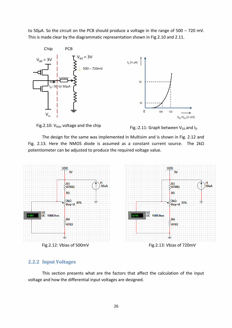
The circuit in Multisim that was used to produce the required results is shown in
Fig.2.8 and Fig.2.9:
Fig 2.8: Circuit for producing 50µA Fig 2.9: Circuit for producing 150µA
2.2.1.3 Vbias
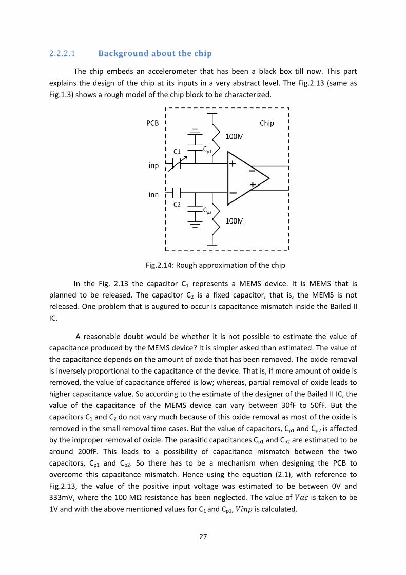
Vbias is the bias voltage that is supplied to the chip. The specification for the voltage
value is that the pin 5 of the Bailed II IC is unconnected by default. But when it is connected,
a NMOS diode inside the chip is connected and it produces a current that varies from -50µA
26
to 50µA. So the circuit on the PCB should produce a voltage in the range of 500 – 720 mV.
This is made clear by the diagrammatic representation shown in Fig.2.10 and 2.11.
Fig.2.10: Vbias voltage and the chip
Fig.:2.11: Graph between VGS and ID
The design for the same was implemented in Multisim and is shown in Fig. 2.12 and
Fig. 2.13. Here the NMOS diode is assumed as a constant current source. The 2kΩ
potentiometer can be adjusted to produce the required voltage value.
Fig.2.12: Vbias of 500mV Fig.2.13: Vbias of 720mV
2.2.2 Input Voltages
This section presents what are the factors that affect the calculation of the input
voltage and how the differential input voltages are designed.
27
2.2.2.1 Background about the chip
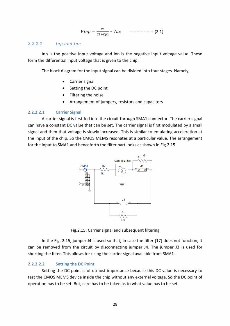
The chip embeds an accelerometer that has been a black box till now. This part
explains the design of the chip at its inputs in a very abstract level. The Fig.2.13 (same as
Fig.1.3) shows a rough model of the chip block to be characterized.
Fig.2.14: Rough approximation of the chip
In the Fig. 2.13 the capacitor C1 represents a MEMS device. It is MEMS that is
planned to be released. The capacitor C2 is a fixed capacitor, that is, the MEMS is not
released. One problem that is augured to occur is capacitance mismatch inside the Bailed II
IC.
A reasonable doubt would be whether it is not possible to estimate the value of
capacitance produced by the MEMS device? It is simpler asked than estimated. The value of
the capacitance depends on the amount of oxide that has been removed. The oxide removal
is inversely proportional to the capacitance of the device. That is, if more amount of oxide is
removed, the value of capacitance offered is low; whereas, partial removal of oxide leads to
higher capacitance value. So according to the estimate of the designer of the Bailed II IC, the
value of the capacitance of the MEMS device can vary between 30fF to 50fF. But the
capacitors C1 and C2 do not vary much because of this oxide removal as most of the oxide is
removed in the small removal time cases. But the value of capacitors, Cp1 and Cp2 is affected
by the improper removal of oxide. The parasitic capacitances Cp1 and Cp2 are estimated to be
around 200fF. This leads to a possibility of capacitance mismatch between the two
capacitors, Cp1 and Cp2. So there has to be a mechanism when designing the PCB to
overcome this capacitance mismatch. Hence using the equation (2.1), with reference to
Fig.2.13, the value of the positive input voltage was estimated to be between 0V and
333mV, where the 100 MΩ resistance has been neglected. The value of is taken to be
1V and with the above mentioned values for C1 and Cp1, is calculated.
28
----------------- (2.1)
2.2.2.2 Inp and Inn
Inp is the positive input voltage and inn is the negative input voltage value. These
form the differential input voltage that is given to the chip.
The block diagram for the input signal can be divided into four stages. Namely,
Carrier signal
Setting the DC point
Filtering the noise
Arrangement of jumpers, resistors and capacitors
2.2.2.2.1 Carrier Signal
A carrier signal is first fed into the circuit through SMA1 connector. The carrier signal
can have a constant DC value that can be set. The carrier signal is first modulated by a small
signal and then that voltage is slowly increased. This is similar to emulating acceleration at
the input of the chip. So the CMOS MEMS resonates at a particular value. The arrangement
for the input to SMA1 and henceforth the filter part looks as shown in Fig.2.15.
Fig.2.15: Carrier signal and subsequent filtering
In the Fig. 2.15, jumper J4 is used so that, in case the filter [17] does not function, it
can be removed from the circuit by disconnecting jumper J4. The jumper J3 is used for
shorting the filter. This allows for using the carrier signal available from SMA1.
2.2.2.2.2 Setting the DC Point
Setting the DC point is of utmost importance because this DC value is necessary to
test the CMOS MEMS device inside the chip without any external voltage. So the DC point of
operation has to be set. But, care has to be taken as to what value has to be set.
29
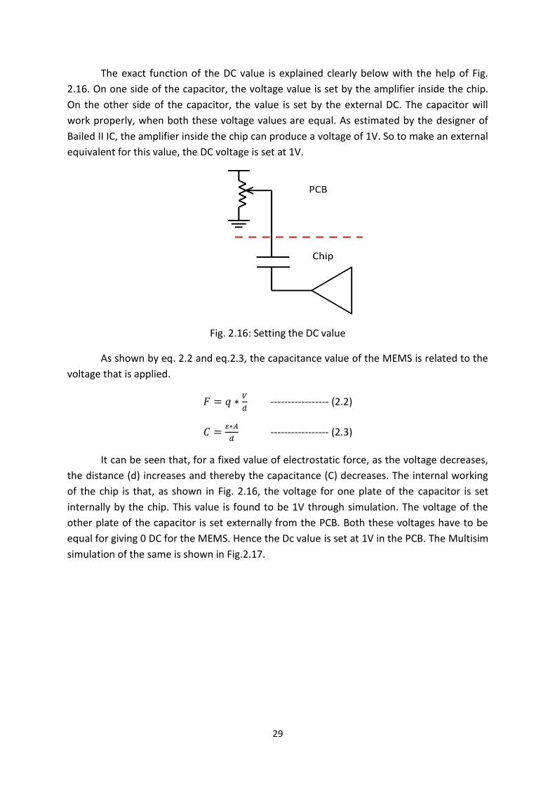
The exact function of the DC value is explained clearly below with the help of Fig.
2.16. On one side of the capacitor, the voltage value is set by the amplifier inside the chip.
On the other side of the capacitor, the value is set by the external DC. The capacitor will
work properly, when both these voltage values are equal. As estimated by the designer of
Bailed II IC, the amplifier inside the chip can produce a voltage of 1V. So to make an external
equivalent for this value, the DC voltage is set at 1V.
Fig. 2.16: Setting the DC value
As shown by eq. 2.2 and eq.2.3, the capacitance value of the MEMS is related to the
voltage that is applied.
----------------- (2.2)
----------------- (2.3)
It can be seen that, for a fixed value of electrostatic force, as the voltage decreases,
the distance (d) increases and thereby the capacitance (C) decreases. The internal working
of the chip is that, as shown in Fig. 2.16, the voltage for one plate of the capacitor is set
internally by the chip. This value is found to be 1V through simulation. The voltage of the
other plate of the capacitor is set externally from the PCB. Both these voltages have to be
equal for giving 0 DC for the MEMS. Hence the Dc value is set at 1V in the PCB. The Multisim
simulation of the same is shown in Fig.2.17.
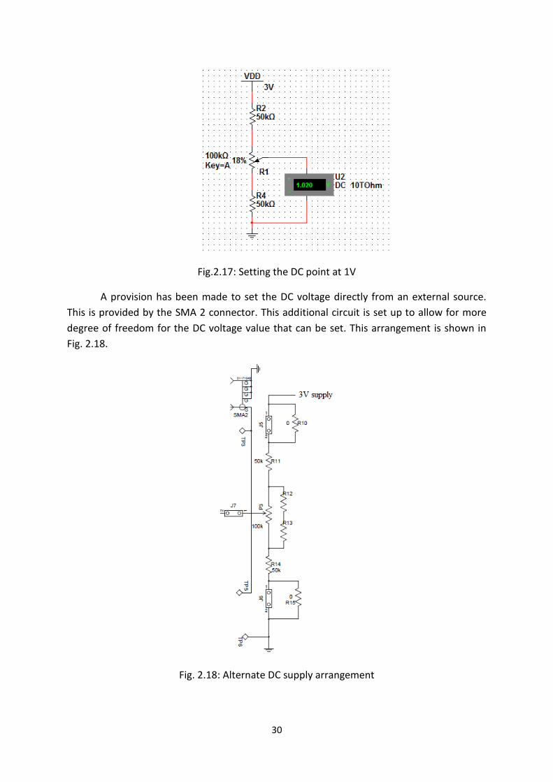
30
Fig.2.17: Setting the DC point at 1V
A provision has been made to set the DC voltage directly from an external source.
This is provided by the SMA 2 connector. This additional circuit is set up to allow for more
degree of freedom for the DC voltage value that can be set. This arrangement is shown in
Fig. 2.18.
Fig. 2.18: Alternate DC supply arrangement
31
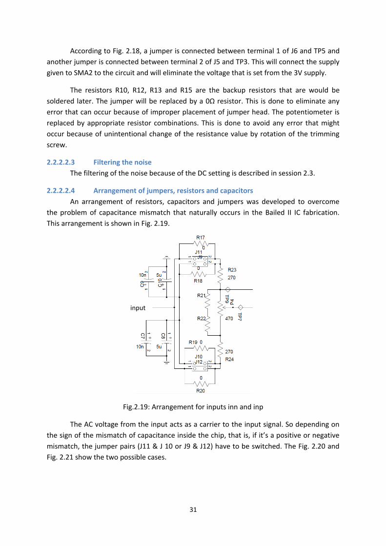
According to Fig. 2.18, a jumper is connected between terminal 1 of J6 and TP5 and
another jumper is connected between terminal 2 of J5 and TP3. This will connect the supply
given to SMA2 to the circuit and will eliminate the voltage that is set from the 3V supply.
The resistors R10, R12, R13 and R15 are the backup resistors that are would be
soldered later. The jumper will be replaced by a 0Ω resistor. This is done to eliminate any
error that can occur because of improper placement of jumper head. The potentiometer is
replaced by appropriate resistor combinations. This is done to avoid any error that might
occur because of unintentional change of the resistance value by rotation of the trimming
screw.
2.2.2.2.3 Filtering the noise
The filtering of the noise because of the DC setting is described in session 2.3.
2.2.2.2.4 Arrangement of jumpers, resistors and capacitors
An arrangement of resistors, capacitors and jumpers was developed to overcome
the problem of capacitance mismatch that naturally occurs in the Bailed II IC fabrication.
This arrangement is shown in Fig. 2.19.
Fig.2.19: Arrangement for inputs inn and inp
The AC voltage from the input acts as a carrier to the input signal. So depending on
the sign of the mismatch of capacitance inside the chip, that is, if it’s a positive or negative
mismatch, the jumper pairs (J11 & J 10 or J9 & J12) have to be switched. The Fig. 2.20 and
Fig. 2.21 show the two possible cases.
input
32
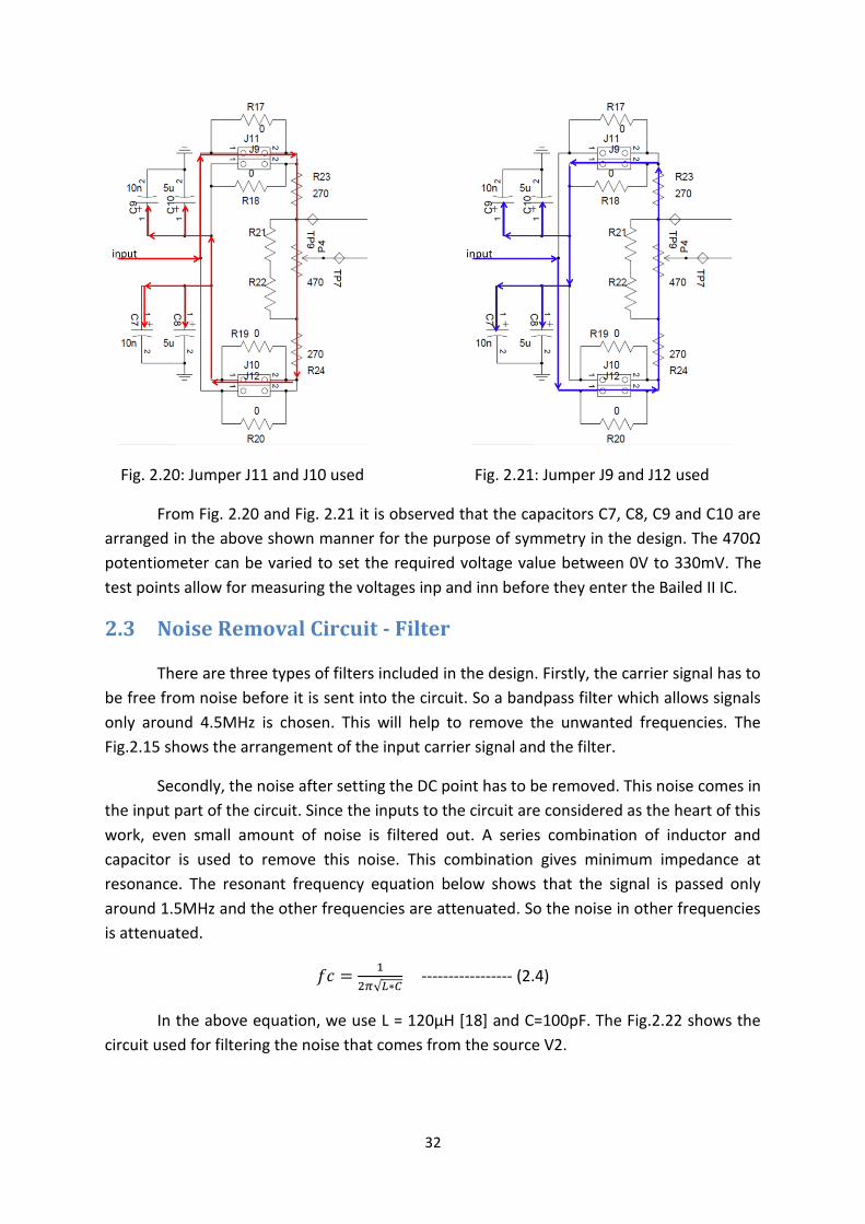
Fig. 2.20: Jumper J11 and J10 used
Fig. 2.21: Jumper J9 and J12 used
From Fig. 2.20 and Fig. 2.21 it is observed that the capacitors C7, C8, C9 and C10 are
arranged in the above shown manner for the purpose of symmetry in the design. The 470Ω
potentiometer can be varied to set the required voltage value between 0V to 330mV. The
test points allow for measuring the voltages inp and inn before they enter the Bailed II IC.
2.3 Noise Removal Circuit - Filter
There are three types of filters included in the design. Firstly, the carrier signal has to
be free from noise before it is sent into the circuit. So a bandpass filter which allows signals
only around 4.5MHz is chosen. This will help to remove the unwanted frequencies. The
Fig.2.15 shows the arrangement of the input carrier signal and the filter.
Secondly, the noise after setting the DC point has to be removed. This noise comes in
the input part of the circuit. Since the inputs to the circuit are considered as the heart of this
work, even small amount of noise is filtered out. A series combination of inductor and
capacitor is used to remove this noise. This combination gives minimum impedance at
resonance. The resonant frequency equation below shows that the signal is passed only
around 1.5MHz and the other frequencies are attenuated. So the noise in other frequencies
is attenuated.
----------------- (2.4)
In the above equation, we use L = 120µH [18] and C=100pF. The Fig.2.22 shows the
circuit used for filtering the noise that comes from the source V2.
34
Fig. 2.22: Noise filtering Circuit
In Fig.2.22, the 3V indicates the DC voltage. V1 has a DC voltage value of 0V and an
AC Analysis magnitude of 1V. The resistor R5 is the 1kΩ that comes before the filter in the
schematic in Fig. 2.15. The resistor R6 and capacitor C3 are the values that produce the
voltage value of 0V to 330mV mentioned in section 2.2.2.2.4. It can also be observed that
the DC signal finds high impedance at the capacitor C1. This filters the noise through the
inductor. The AC signal is grounded through the capacitor C1. Noise analysis was done for
the circuit shown in Fig. 2.22. The result shows 24.9% reduction in noise. The Fig. 2.23 shows
this result.
Fig. 2.23 : Noise analysis result
Also, in noise analysis, total noise measurement was done with and without the
inductor capacitor pair. The integrated noise at the Vnoi node without the combination is
165.7nV and the same when the inductor capacitor pair is introduced into the circuit is
82.9nV.

35
Thirdly, the noise that is inherently produced from the 3V/5V supply should be
removed before it reaches the chip. The mechanism that is used as a standard design in
many places of the circuit is shown in Fig.2.24.
Fig. 2.24: Noise removal circuit
In the Fig.2.24, the capacitor C1 of 10µF capacitance filters out the low frequency
noise signal. Filter F1 is a suppression filter with capacitance of 100pF filters out the high
frequency noise around the frequency of 10 MHz.
2.4 Amplifier
The output of the Bailed II IC has to be amplified in order to take measurements. So
an amplifier at the output is required. A gain of 10 was considered to be a good value. The
constraints on the value of resistors gave rise to the need to use cascaded amplifier stages.
The amplifiers are coupled using AC coupling. AC coupling was used so that only the AC
signal passes from one stage of the amplifier to the next. In other words, it helps to isolate
the DC bias settings of the two coupled stages.
The amplifier used is AD8138ARMZ [19]. Care was taken not to allow the amplifier to
go into saturation. The Fig.2.25 shows the cascaded amplifier stages.
Fig. 2.25: Cascaded stages of amplifier
The gain of the amplifier is calculated by the formula given in eq.2.5.
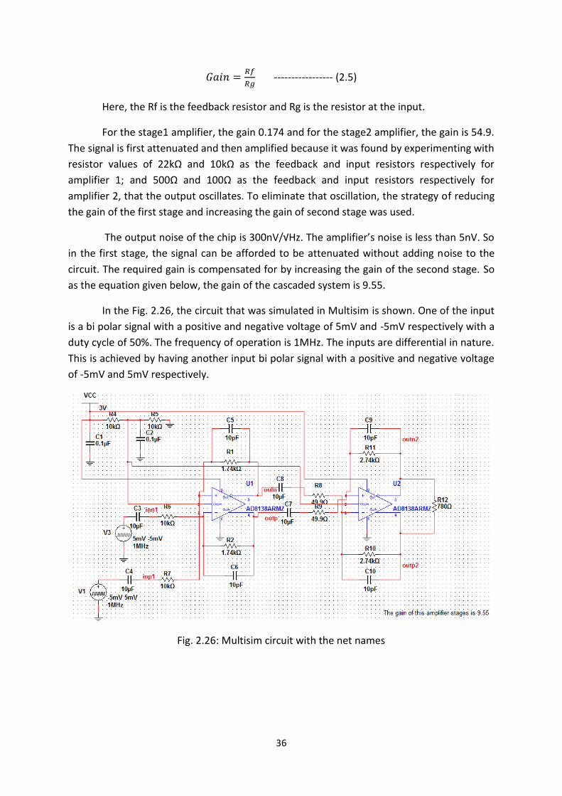
36
----------------- (2.5)
Here, the Rf is the feedback resistor and Rg is the resistor at the input.
For the stage1 amplifier, the gain 0.174 and for the stage2 amplifier, the gain is 54.9.
The signal is first attenuated and then amplified because it was found by experimenting with
resistor values of 22kΩ and 10kΩ as the feedback and input resistors respectively for
amplifier 1; and 500Ω and 100Ω as the feedback and input resistors respectively for
amplifier 2, that the output oscillates. To eliminate that oscillation, the strategy of reducing
the gain of the first stage and increasing the gain of second stage was used.
The output noise of the chip is 300nV/√Hz. The amplifier’s noise is less than 5nV. So
in the first stage, the signal can be afforded to be attenuated without adding noise to the
circuit. The required gain is compensated for by increasing the gain of the second stage. So
as the equation given below, the gain of the cascaded system is 9.55.
In the Fig. 2.26, the circuit that was simulated in Multisim is shown. One of the input
is a bi polar signal with a positive and negative voltage of 5mV and -5mV respectively with a
duty cycle of 50%. The frequency of operation is 1MHz. The inputs are differential in nature.
This is achieved by having another input bi polar signal with a positive and negative voltage
of -5mV and 5mV respectively.
Fig. 2.26: Multisim circuit with the net names
37
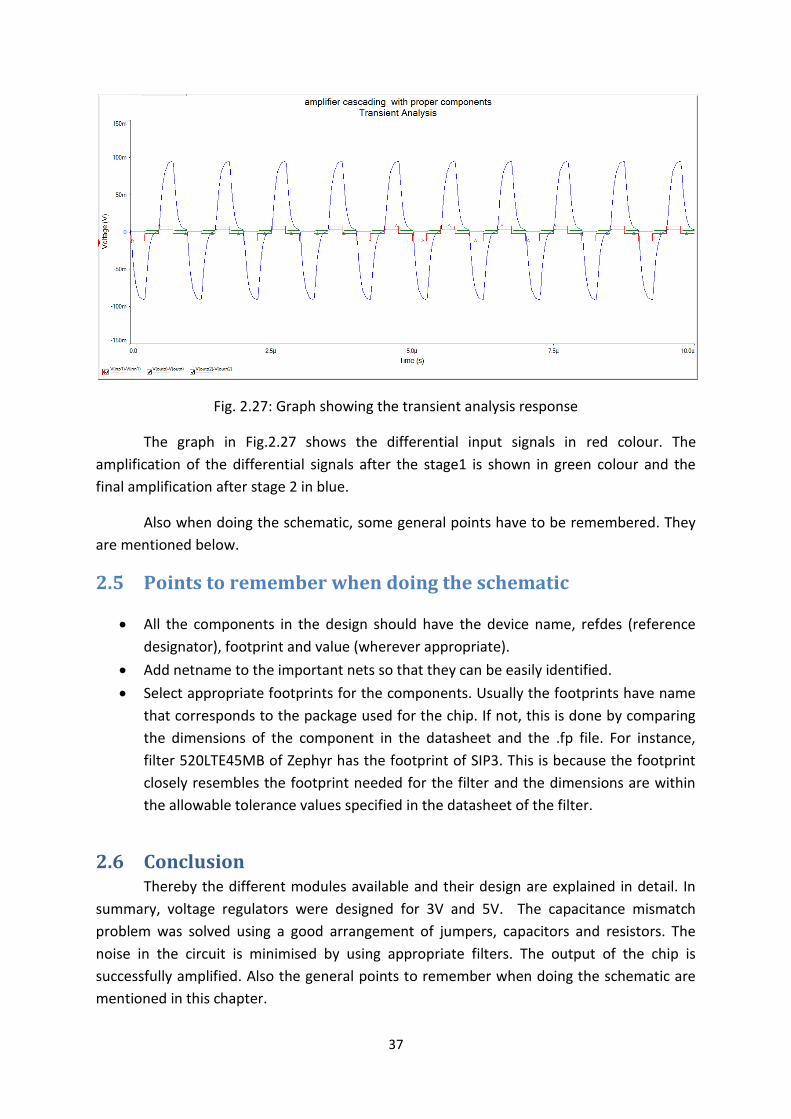
Fig. 2.27: Graph showing the transient analysis response
The graph in Fig.2.27 shows the differential input signals in red colour. The
amplification of the differential signals after the stage1 is shown in green colour and the
final amplification after stage 2 in blue.
Also when doing the schematic, some general points have to be remembered. They
are mentioned below.
2.5 Points to remember when doing the schematic
All the components in the design should have the device name, refdes (reference
designator), footprint and value (wherever appropriate).
Add netname to the important nets so that they can be easily identified.
Select appropriate footprints for the components. Usually the footprints have name
that corresponds to the package used for the chip. If not, this is done by comparing
the dimensions of the component in the datasheet and the .fp file. For instance,
filter 520LTE45MB of Zephyr has the footprint of SIP3. This is because the footprint
closely resembles the footprint needed for the filter and the dimensions are within
the allowable tolerance values specified in the datasheet of the filter.
2.6 Conclusion Thereby the different modules available and their design are explained in detail. In
summary, voltage regulators were designed for 3V and 5V. The capacitance mismatch
problem was solved using a good arrangement of jumpers, capacitors and resistors. The
noise in the circuit is minimised by using appropriate filters. The output of the chip is
successfully amplified. Also the general points to remember when doing the schematic are
mentioned in this chapter.

38
Chapter3: PCB Design
3.1 - Schematic to PCB Conversion 3.2 - PCB Design Steps 3.3 - Placement of Components 3.4 - Routing and Afterwork 3.5 - Conclusion __________________________________________________________________________________
Now this is not the end. It is not even the beginning of the end. But it is, perhaps, the end of the beginning.
-Winston Churchill
The successful completion of the schematic is the basic and mandatory step for the
development of a PCB. This chapter talks about the steps necessary for conversion of the
schematic developed using gEDA to a successful PCB design. Further, it discusses about the
design rules for placing components and connecting them. Appendix A shows the different
layers in the PCB after the design is complete.
3.1. Schematic to PCB conversion After the schematic is ready, there is one small step that is needed for the transfer of
the symbols and their corresponding footprints from the schematic editor to the PCB. There
are two ways to do this conversion. They are:
Using the command line gsch2pcb
Using the Graphical User Interface, xgsch2pcb
The second method was used for the conversion of schematic to PCB when
developing this work. The steps followed for the same are as follows:
Open a text editor.
Type a text, which specifies the filename of the schematic, the directory which
contains the components and finally the name of the PCB file. A sample of the text is
given below:
schematics zephyr.sch elements-dir .. output-name zephyr
Save the file with an extension of .gsch2pcb in the working directory.
When this file is double clicked, the schematic whose name is specified in the file will be loaded into the xgsch2pcb graphical interface and the PCB corresponding to it will be created when Update Layout is clicked. This is shown in Fig. 3.1.
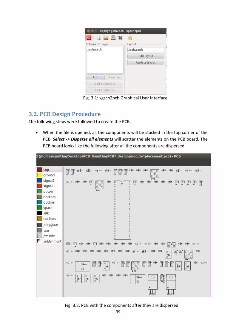
39
Fig. 3.1: xgsch2pcb Graphical User Interface
3.2. PCB Design Procedure The following steps were followed to create the PCB.
When the file is opened, all the components will be stacked in the top corner of the
PCB. Select -> Disperse all elements will scatter the elements on the PCB board. The
PCB board looks like the following after all the components are dispersed.
Fig. 3.2: PCB with the components after they are dispersed
40
If some components are not loaded properly because of improper or missing
footprint, choose an appropriate footprint from the library which contains the
footprints in the schematic editor and then update the PCB design.
Thirdly, draw the rats using the Connects -> Optimize rats nest option.
Then set the size of the board as per the requirements. The PCB board size was set
to 111 mm X 103 mm (width X height). This was selected because the PCB has to be
mounted on a loudspeaker for vibration (acceleration) measurement purpose. The
size of the loudspeaker allows for this size of the PCB. The size of the PCB was set
using File -> Preferences.. -> Sizes.
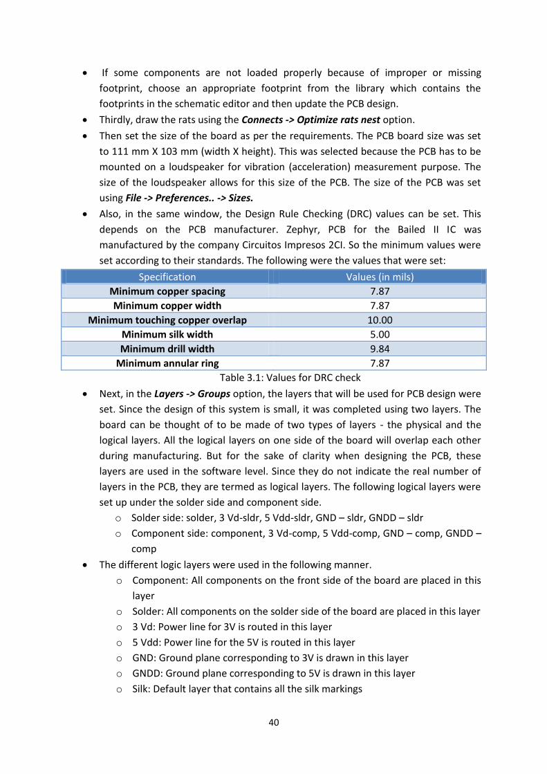
Also, in the same window, the Design Rule Checking (DRC) values can be set. This
depends on the PCB manufacturer. Zephyr, PCB for the Bailed II IC was
manufactured by the company Circuitos Impresos 2CI. So the minimum values were
set according to their standards. The following were the values that were set:
Specification Values (in mils)
Minimum copper spacing 7.87
Minimum copper width 7.87
Minimum touching copper overlap 10.00
Minimum silk width 5.00
Minimum drill width 9.84
Minimum annular ring 7.87
Table 3.1: Values for DRC check
Next, in the Layers -> Groups option, the layers that will be used for PCB design were
set. Since the design of this system is small, it was completed using two layers. The
board can be thought of to be made of two types of layers - the physical and the
logical layers. All the logical layers on one side of the board will overlap each other
during manufacturing. But for the sake of clarity when designing the PCB, these
layers are used in the software level. Since they do not indicate the real number of
layers in the PCB, they are termed as logical layers. The following logical layers were
set up under the solder side and component side.
o Solder side: solder, 3 Vd-sldr, 5 Vdd-sldr, GND – sldr, GNDD – sldr
o Component side: component, 3 Vd-comp, 5 Vdd-comp, GND – comp, GNDD –
comp
The different logic layers were used in the following manner.
o Component: All components on the front side of the board are placed in this
layer
o Solder: All components on the solder side of the board are placed in this layer
o 3 Vd: Power line for 3V is routed in this layer
o 5 Vdd: Power line for the 5V is routed in this layer
o GND: Ground plane corresponding to 3V is drawn in this layer
o GNDD: Ground plane corresponding to 5V is drawn in this layer
o Silk: Default layer that contains all the silk markings
41
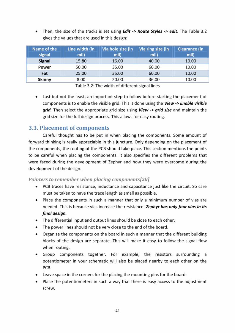
Then, the size of the tracks is set using Edit -> Route Styles -> edit. The Table 3.2
gives the values that are used in this design:
Name of the signal
Line width (in mil)
Via hole size (in mil)
Via ring size (in mil)
Clearance (in mil)
Signal 15.80 16.00 40.00 10.00
Power 50.00 35.00 60.00 10.00
Fat 25.00 35.00 60.00 10.00
Skinny 8.00 20.00 36.00 10.00
Table 3.2: The width of different signal lines
Last but not the least, an important step to follow before starting the placement of
components is to enable the visible grid. This is done using the View -> Enable visible
grid. Then select the appropriate grid size using View -> grid size and maintain the
grid size for the full design process. This allows for easy routing.
3.3. Placement of components Careful thought has to be put in when placing the components. Some amount of
forward thinking is really appreciable in this juncture. Only depending on the placement of
the components, the routing of the PCB should take place. This section mentions the points
to be careful when placing the components. It also specifies the different problems that
were faced during the development of Zephyr and how they were overcome during the
development of the design.
Pointers to remember when placing components[20]
PCB traces have resistance, inductance and capacitance just like the circuit. So care
must be taken to have the trace length as small as possible.
Place the components in such a manner that only a minimum number of vias are
needed. This is because vias increase the resistance. Zephyr has only four vias in its
final design.
The differential input and output lines should be close to each other.
The power lines should not be very close to the end of the board.
Organize the components on the board in such a manner that the different building
blocks of the design are separate. This will make it easy to follow the signal flow
when routing.
Group components together. For example, the resistors surrounding a
potentiometer in your schematic will also be placed nearby to each other on the
PCB.
Leave space in the corners for the placing the mounting pins for the board.
Place the potentiometers in such a way that there is easy access to the adjustment
screw.
42
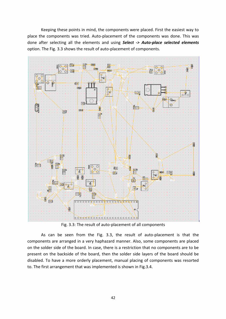
Keeping these points in mind, the components were placed. First the easiest way to
place the components was tried. Auto-placement of the components was done. This was
done after selecting all the elements and using Select -> Auto-place selected elements
option. The Fig. 3.3 shows the result of auto-placement of components.
Fig. 3.3: The result of auto-placement of all components
As can be seen from the Fig. 3.3, the result of auto-placement is that the
components are arranged in a very haphazard manner. Also, some components are placed
on the solder side of the board. In case, there is a restriction that no components are to be
present on the backside of the board, then the solder side layers of the board should be
disabled. To have a more orderly placement, manual placing of components was resorted
to. The first arrangement that was implemented is shown in Fig.3.4.
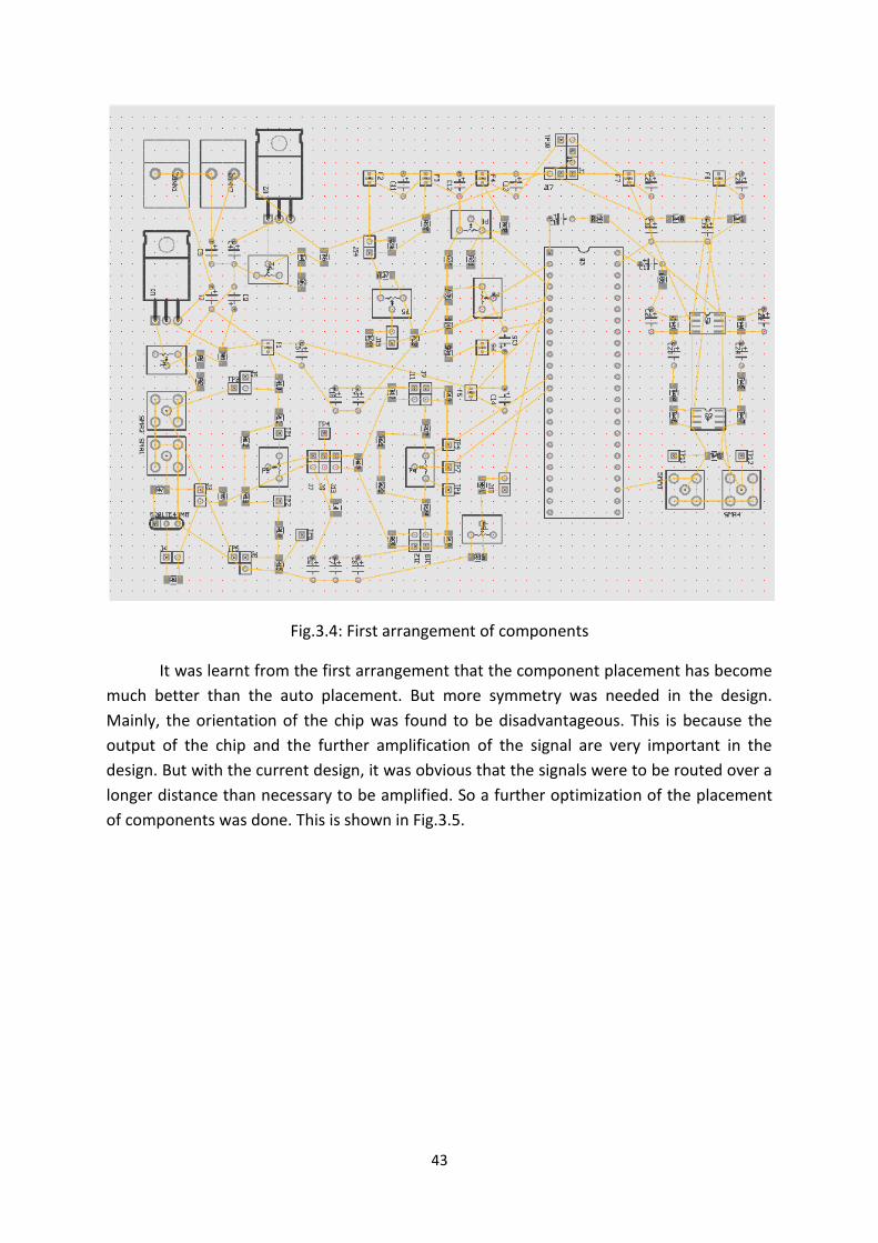
43
Fig.3.4: First arrangement of components
It was learnt from the first arrangement that the component placement has become
much better than the auto placement. But more symmetry was needed in the design.
Mainly, the orientation of the chip was found to be disadvantageous. This is because the
output of the chip and the further amplification of the signal are very important in the
design. But with the current design, it was obvious that the signals were to be routed over a
longer distance than necessary to be amplified. So a further optimization of the placement
of components was done. This is shown in Fig.3.5.
44
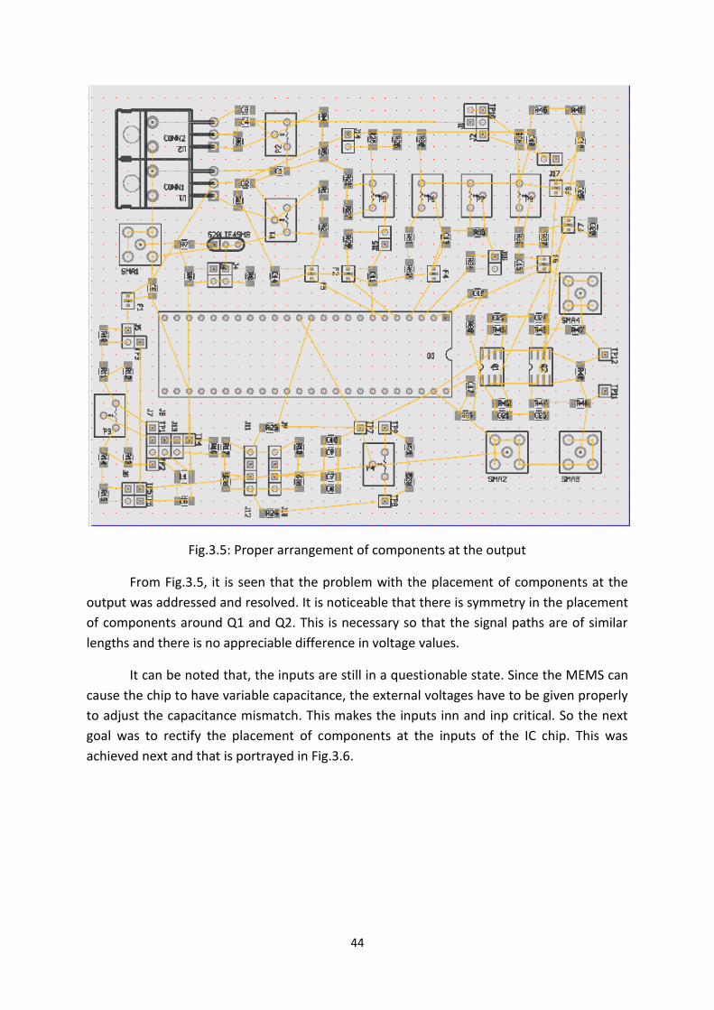
Fig.3.5: Proper arrangement of components at the output
From Fig.3.5, it is seen that the problem with the placement of components at the
output was addressed and resolved. It is noticeable that there is symmetry in the placement
of components around Q1 and Q2. This is necessary so that the signal paths are of similar
lengths and there is no appreciable difference in voltage values.
It can be noted that, the inputs are still in a questionable state. Since the MEMS can
cause the chip to have variable capacitance, the external voltages have to be given properly
to adjust the capacitance mismatch. This makes the inputs inn and inp critical. So the next
goal was to rectify the placement of components at the inputs of the IC chip. This was
achieved next and that is portrayed in Fig.3.6.
45
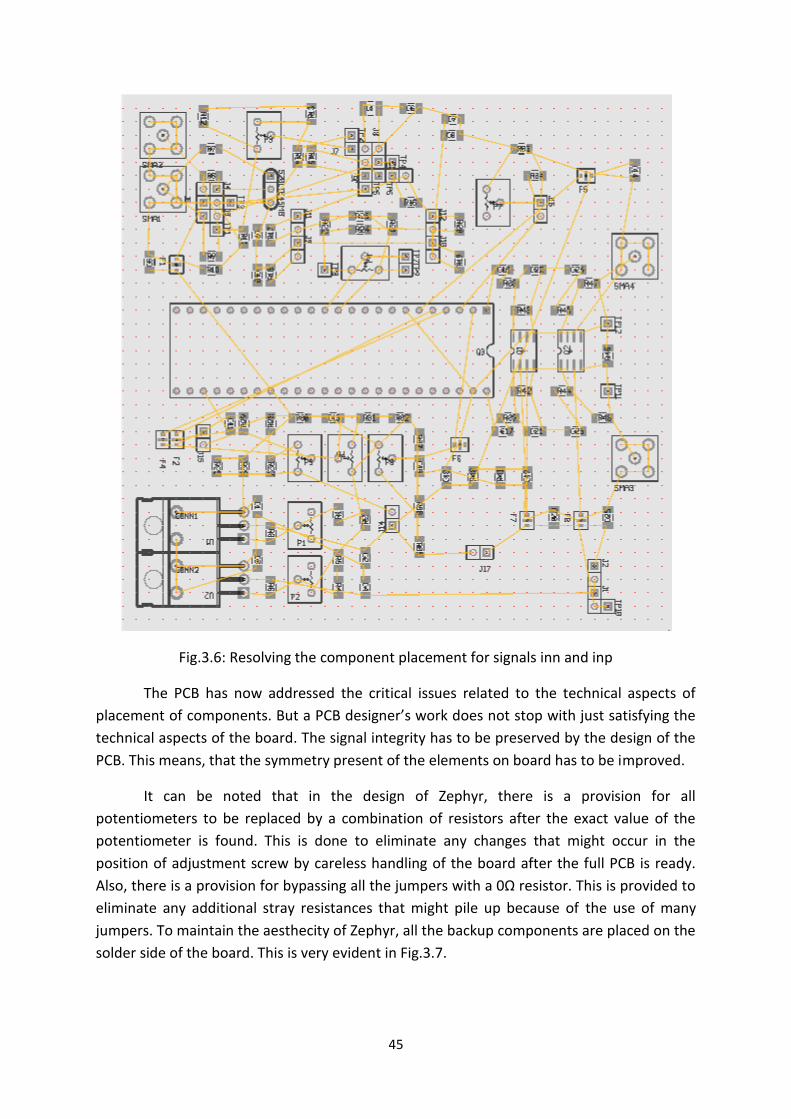
Fig.3.6: Resolving the component placement for signals inn and inp
The PCB has now addressed the critical issues related to the technical aspects of
placement of components. But a PCB designer’s work does not stop with just satisfying the
technical aspects of the board. The signal integrity has to be preserved by the design of the
PCB. This means, that the symmetry present of the elements on board has to be improved.
It can be noted that in the design of Zephyr, there is a provision for all
potentiometers to be replaced by a combination of resistors after the exact value of the
potentiometer is found. This is done to eliminate any changes that might occur in the
position of adjustment screw by careless handling of the board after the full PCB is ready.
Also, there is a provision for bypassing all the jumpers with a 0Ω resistor. This is provided to
eliminate any additional stray resistances that might pile up because of the use of many
jumpers. To maintain the aesthecity of Zephyr, all the backup components are placed on the
solder side of the board. This is very evident in Fig.3.7.
46
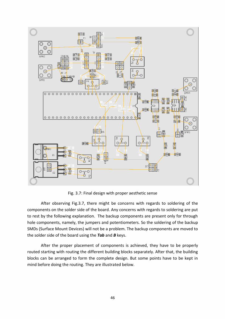
Fig. 3.7: Final design with proper aesthetic sense
After observing Fig.3.7, there might be concerns with regards to soldering of the
components on the solder side of the board. Any concerns with regards to soldering are put
to rest by the following explanation. The backup components are present only for through
hole components, namely, the jumpers and potentiometers. So the soldering of the backup
SMDs (Surface Mount Devices) will not be a problem. The backup components are moved to
the solder side of the board using the Tab and B keys.
After the proper placement of components is achieved, they have to be properly
routed starting with routing the different building blocks separately. After that, the building
blocks can be arranged to form the complete design. But some points have to be kept in
mind before doing the routing. They are illustrated below.
47
3.4. Routing and after work Points to remember during routing and after [20]
Avoid 90 degree corners. Straight lines with 45 degree corners are preferable.
Every new footprint and part should have a human readable description for the sake
of clarity.
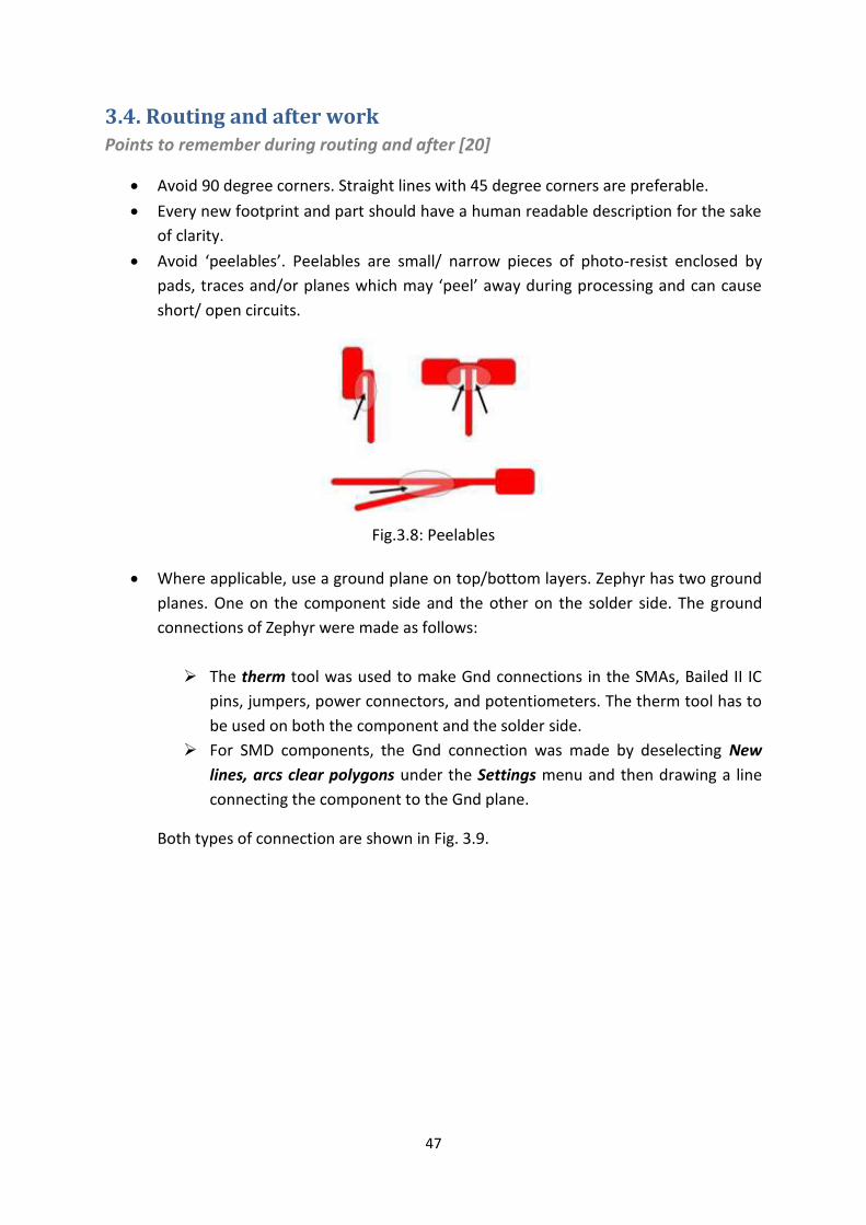
Avoid ‘peelables’. Peelables are small/ narrow pieces of photo-resist enclosed by
pads, traces and/or planes which may ‘peel’ away during processing and can cause
short/ open circuits.
Fig.3.8: Peelables
Where applicable, use a ground plane on top/bottom layers. Zephyr has two ground
planes. One on the component side and the other on the solder side. The ground
connections of Zephyr were made as follows:
The therm tool was used to make Gnd connections in the SMAs, Bailed II IC
pins, jumpers, power connectors, and potentiometers. The therm tool has to
be used on both the component and the solder side.
For SMD components, the Gnd connection was made by deselecting New
lines, arcs clear polygons under the Settings menu and then drawing a line
connecting the component to the Gnd plane.
Both types of connection are shown in Fig. 3.9.
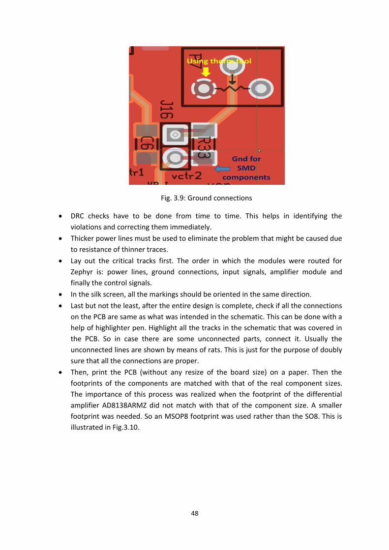
48
Fig. 3.9: Ground connections
DRC checks have to be done from time to time. This helps in identifying the
violations and correcting them immediately.
Thicker power lines must be used to eliminate the problem that might be caused due
to resistance of thinner traces.
Lay out the critical tracks first. The order in which the modules were routed for
Zephyr is: power lines, ground connections, input signals, amplifier module and
finally the control signals.
In the silk screen, all the markings should be oriented in the same direction.
Last but not the least, after the entire design is complete, check if all the connections
on the PCB are same as what was intended in the schematic. This can be done with a
help of highlighter pen. Highlight all the tracks in the schematic that was covered in
the PCB. So in case there are some unconnected parts, connect it. Usually the
unconnected lines are shown by means of rats. This is just for the purpose of doubly
sure that all the connections are proper.
Then, print the PCB (without any resize of the board size) on a paper. Then the
footprints of the components are matched with that of the real component sizes.
The importance of this process was realized when the footprint of the differential
amplifier AD8138ARMZ did not match with that of the component size. A smaller
footprint was needed. So an MSOP8 footprint was used rather than the SO8. This is
illustrated in Fig.3.10.
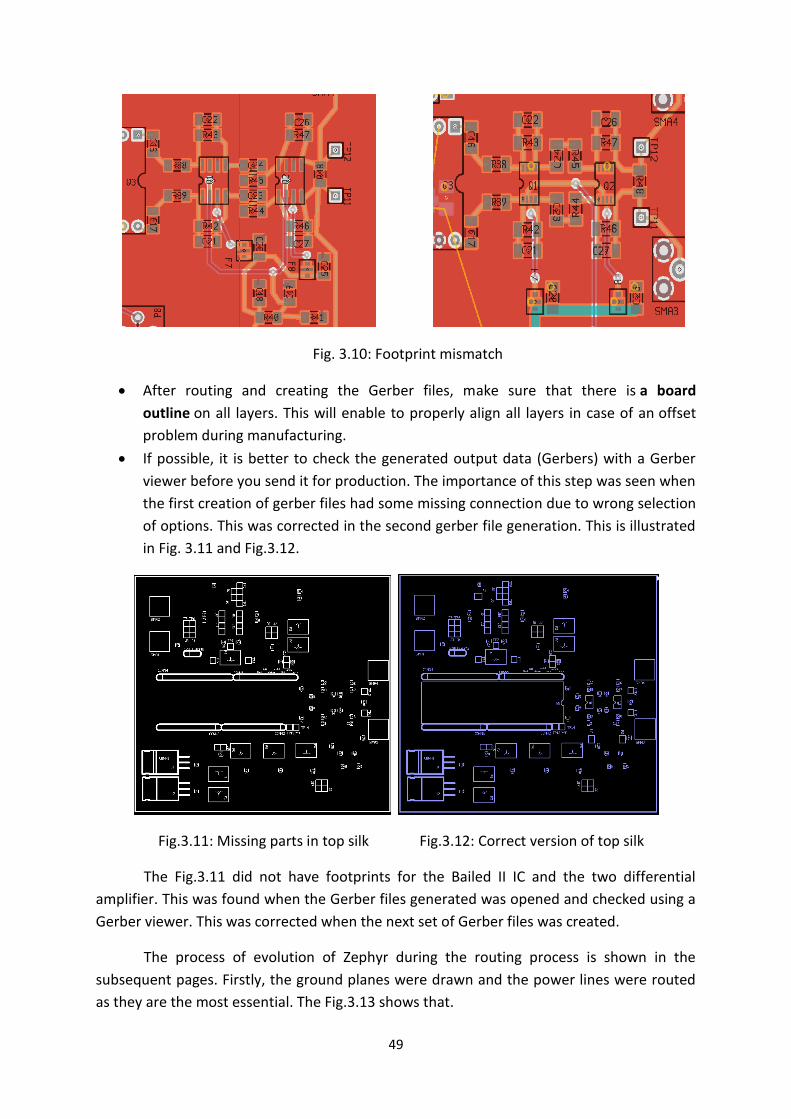
49
Fig. 3.10: Footprint mismatch
After routing and creating the Gerber files, make sure that there is a board
outline on all layers. This will enable to properly align all layers in case of an offset
problem during manufacturing.
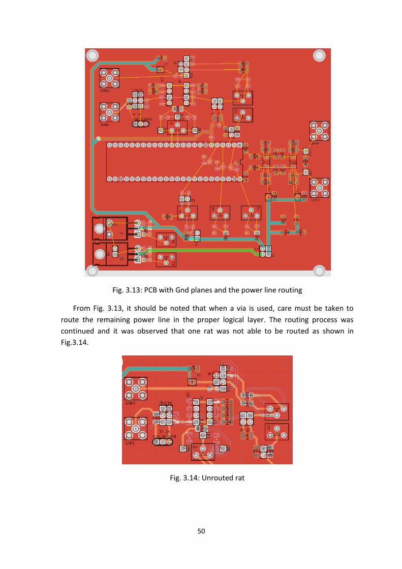
If possible, it is better to check the generated output data (Gerbers) with a Gerber
viewer before you send it for production. The importance of this step was seen when
the first creation of gerber files had some missing connection due to wrong selection
of options. This was corrected in the second gerber file generation. This is illustrated
in Fig. 3.11 and Fig.3.12.
Fig.3.11: Missing parts in top silk Fig.3.12: Correct version of top silk
The Fig.3.11 did not have footprints for the Bailed II IC and the two differential
amplifier. This was found when the Gerber files generated was opened and checked using a
Gerber viewer. This was corrected when the next set of Gerber files was created.
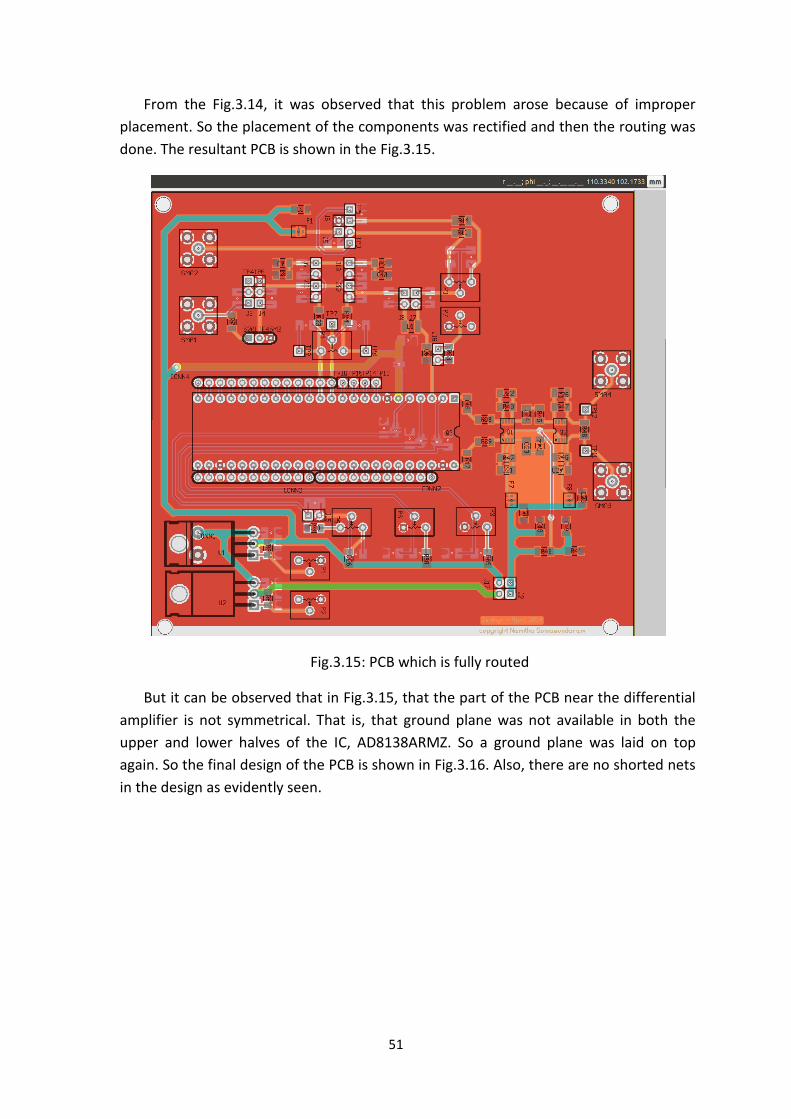
The process of evolution of Zephyr during the routing process is shown in the
subsequent pages. Firstly, the ground planes were drawn and the power lines were routed
as they are the most essential. The Fig.3.13 shows that.
50
Fig. 3.13: PCB with Gnd planes and the power line routing
From Fig. 3.13, it should be noted that when a via is used, care must be taken to
route the remaining power line in the proper logical layer. The routing process was
continued and it was observed that one rat was not able to be routed as shown in
Fig.3.14.
Fig. 3.14: Unrouted rat
51
From the Fig.3.14, it was observed that this problem arose because of improper
placement. So the placement of the components was rectified and then the routing was
done. The resultant PCB is shown in the Fig.3.15.
Fig.3.15: PCB which is fully routed
But it can be observed that in Fig.3.15, that the part of the PCB near the differential
amplifier is not symmetrical. That is, that ground plane was not available in both the
upper and lower halves of the IC, AD8138ARMZ. So a ground plane was laid on top
again. So the final design of the PCB is shown in Fig.3.16. Also, there are no shorted nets
in the design as evidently seen.
52
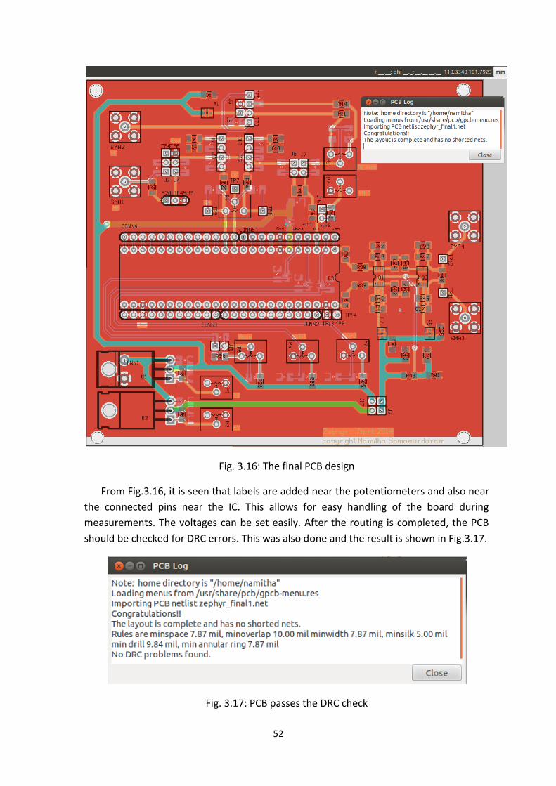
Fig. 3.16: The final PCB design
From Fig.3.16, it is seen that labels are added near the potentiometers and also near
the connected pins near the IC. This allows for easy handling of the board during
measurements. The voltages can be set easily. After the routing is completed, the PCB
should be checked for DRC errors. This was also done and the result is shown in Fig.3.17.
Fig. 3.17: PCB passes the DRC check

53
The PCB files now have to be converted into Gerber files and sent to the
manufacturer. This can be done File -> Export layout…-> gerber and check all layers.
3.5. Conclusion This chapter showed the rules that are to be followed when the components are
placed on the PCB. It also illustrated the points to keep in mind when routing the placed
components. The way Zephyr is modeled was also shown clearly with diagrammatic
explanations.
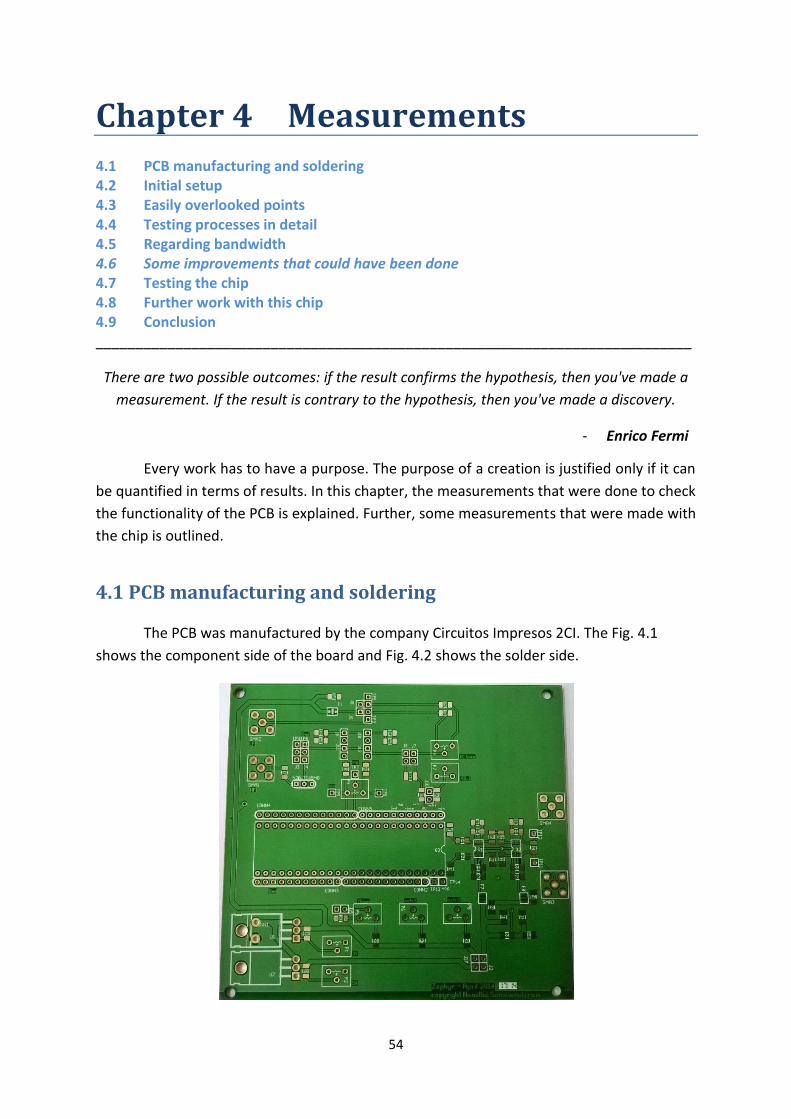
54
Chapter 4 Measurements
4.1 PCB manufacturing and soldering 4.2 Initial setup 4.3 Easily overlooked points 4.4 Testing processes in detail 4.5 Regarding bandwidth 4.6 Some improvements that could have been done 4.7 Testing the chip 4.8 Further work with this chip 4.9 Conclusion ___________________________________________________________________________
There are two possible outcomes: if the result confirms the hypothesis, then you've made a
measurement. If the result is contrary to the hypothesis, then you've made a discovery.
- Enrico Fermi
Every work has to have a purpose. The purpose of a creation is justified only if it can
be quantified in terms of results. In this chapter, the measurements that were done to check
the functionality of the PCB is explained. Further, some measurements that were made with
the chip is outlined.
4.1 PCB manufacturing and soldering
The PCB was manufactured by the company Circuitos Impresos 2CI. The Fig. 4.1
shows the component side of the board and Fig. 4.2 shows the solder side.
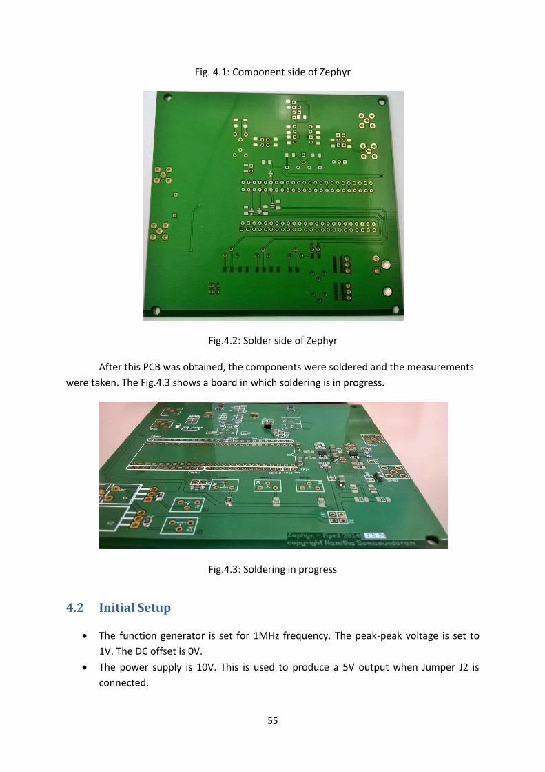
55
Fig. 4.1: Component side of Zephyr
Fig.4.2: Solder side of Zephyr
After this PCB was obtained, the components were soldered and the measurements
were taken. The Fig.4.3 shows a board in which soldering is in progress.
Fig.4.3: Soldering in progress
4.2 Initial Setup
The function generator is set for 1MHz frequency. The peak-peak voltage is set to
1V. The DC offset is 0V.
The power supply is 10V. This is used to produce a 5V output when Jumper J2 is
connected.
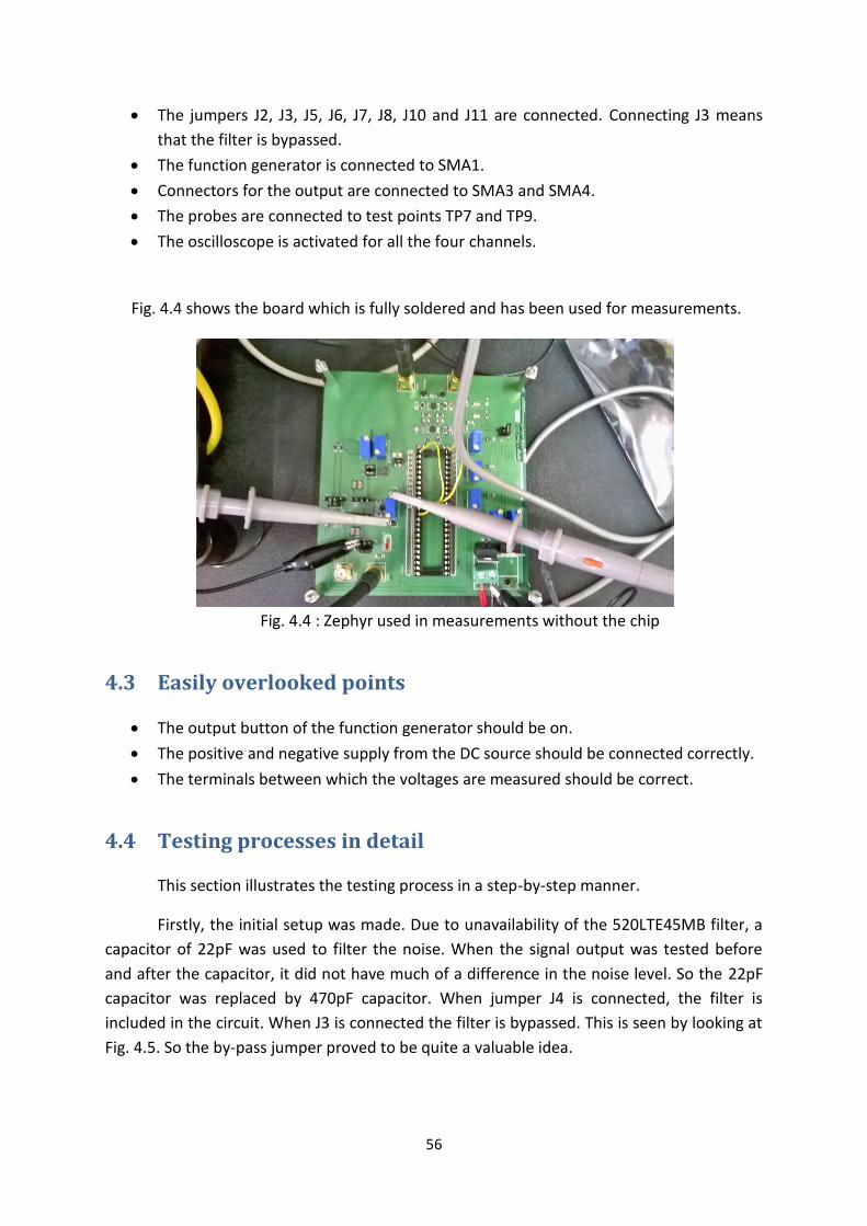
56
The jumpers J2, J3, J5, J6, J7, J8, J10 and J11 are connected. Connecting J3 means
that the filter is bypassed.
The function generator is connected to SMA1.
Connectors for the output are connected to SMA3 and SMA4.
The probes are connected to test points TP7 and TP9.
The oscilloscope is activated for all the four channels.
Fig. 4.4 shows the board which is fully soldered and has been used for measurements.
Fig. 4.4 : Zephyr used in measurements without the chip
4.3 Easily overlooked points
The output button of the function generator should be on.
The positive and negative supply from the DC source should be connected correctly.
The terminals between which the voltages are measured should be correct.
4.4 Testing processes in detail
This section illustrates the testing process in a step-by-step manner.
Firstly, the initial setup was made. Due to unavailability of the 520LTE45MB filter, a
capacitor of 22pF was used to filter the noise. When the signal output was tested before
and after the capacitor, it did not have much of a difference in the noise level. So the 22pF
capacitor was replaced by 470pF capacitor. When jumper J4 is connected, the filter is
included in the circuit. When J3 is connected the filter is bypassed. This is seen by looking at
Fig. 4.5. So the by-pass jumper proved to be quite a valuable idea.
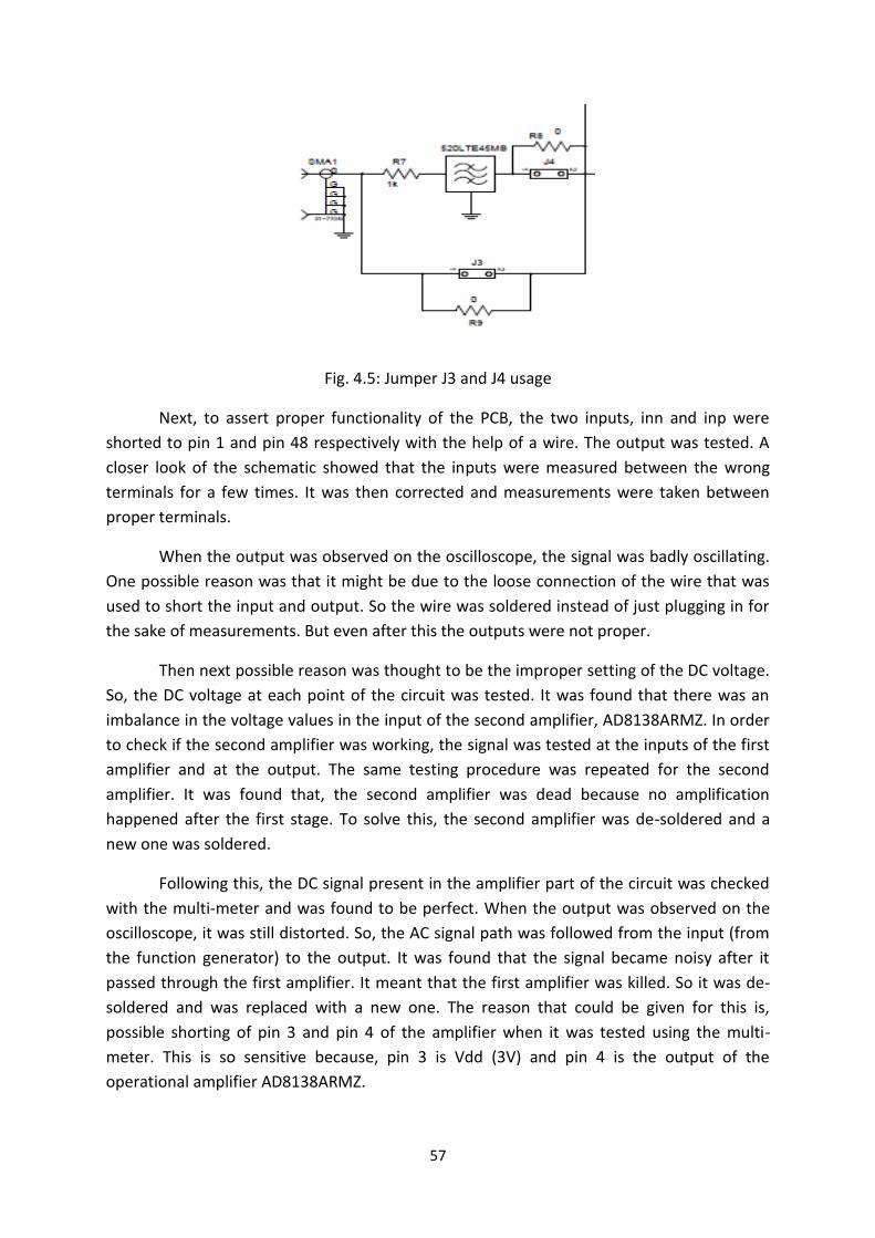
57
Fig. 4.5: Jumper J3 and J4 usage
Next, to assert proper functionality of the PCB, the two inputs, inn and inp were
shorted to pin 1 and pin 48 respectively with the help of a wire. The output was tested. A
closer look of the schematic showed that the inputs were measured between the wrong
terminals for a few times. It was then corrected and measurements were taken between
proper terminals.
When the output was observed on the oscilloscope, the signal was badly oscillating.
One possible reason was that it might be due to the loose connection of the wire that was
used to short the input and output. So the wire was soldered instead of just plugging in for
the sake of measurements. But even after this the outputs were not proper.
Then next possible reason was thought to be the improper setting of the DC voltage.
So, the DC voltage at each point of the circuit was tested. It was found that there was an
imbalance in the voltage values in the input of the second amplifier, AD8138ARMZ. In order
to check if the second amplifier was working, the signal was tested at the inputs of the first
amplifier and at the output. The same testing procedure was repeated for the second
amplifier. It was found that, the second amplifier was dead because no amplification
happened after the first stage. To solve this, the second amplifier was de-soldered and a
new one was soldered.
Following this, the DC signal present in the amplifier part of the circuit was checked
with the multi-meter and was found to be perfect. When the output was observed on the
oscilloscope, it was still distorted. So, the AC signal path was followed from the input (from
the function generator) to the output. It was found that the signal became noisy after it
passed through the first amplifier. It meant that the first amplifier was killed. So it was de-
soldered and was replaced with a new one. The reason that could be given for this is,
possible shorting of pin 3 and pin 4 of the amplifier when it was tested using the multi-
meter. This is so sensitive because, pin 3 is Vdd (3V) and pin 4 is the output of the
operational amplifier AD8138ARMZ.
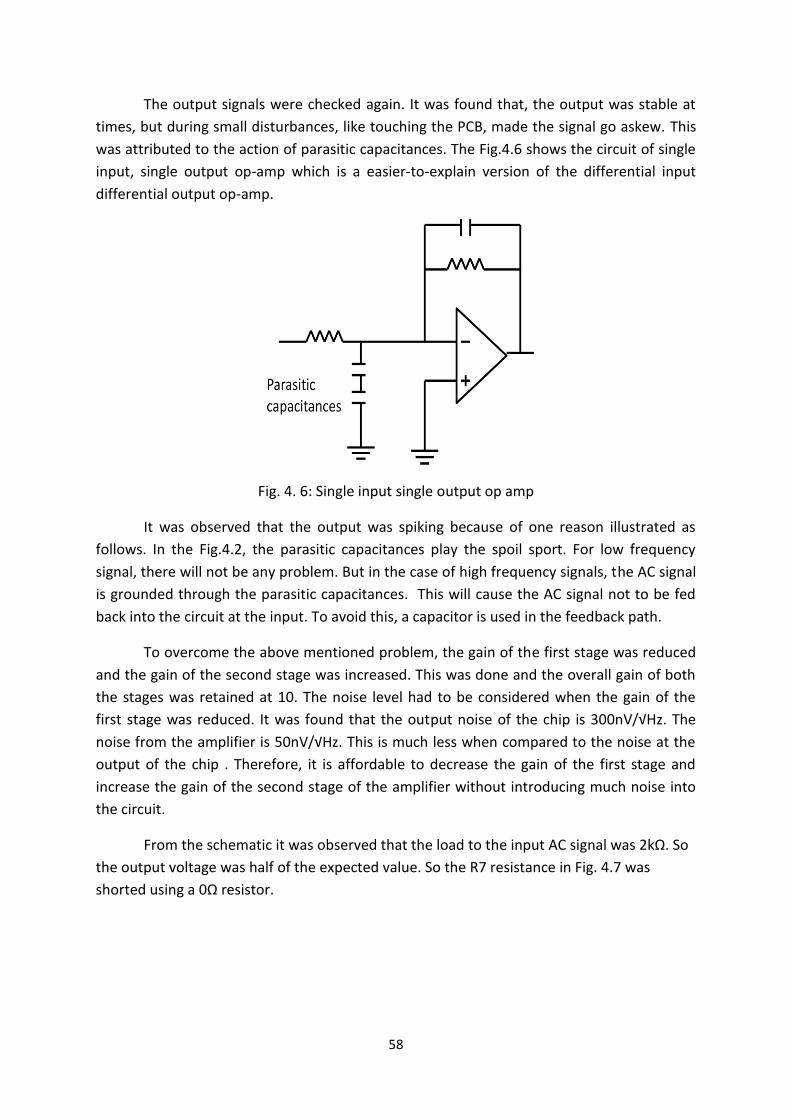
58
The output signals were checked again. It was found that, the output was stable at
times, but during small disturbances, like touching the PCB, made the signal go askew. This
was attributed to the action of parasitic capacitances. The Fig.4.6 shows the circuit of single
input, single output op-amp which is a easier-to-explain version of the differential input
differential output op-amp.
Fig. 4. 6: Single input single output op amp
It was observed that the output was spiking because of one reason illustrated as
follows. In the Fig.4.2, the parasitic capacitances play the spoil sport. For low frequency
signal, there will not be any problem. But in the case of high frequency signals, the AC signal
is grounded through the parasitic capacitances. This will cause the AC signal not to be fed
back into the circuit at the input. To avoid this, a capacitor is used in the feedback path.
To overcome the above mentioned problem, the gain of the first stage was reduced
and the gain of the second stage was increased. This was done and the overall gain of both
the stages was retained at 10. The noise level had to be considered when the gain of the
first stage was reduced. It was found that the output noise of the chip is 300nV/√Hz. The
noise from the amplifier is 50nV/√Hz. This is much less when compared to the noise at the
output of the chip . Therefore, it is affordable to decrease the gain of the first stage and
increase the gain of the second stage of the amplifier without introducing much noise into
the circuit.
From the schematic it was observed that the load to the input AC signal was 2kΩ. So
the output voltage was half of the expected value. So the R7 resistance in Fig. 4.7 was
shorted using a 0Ω resistor.
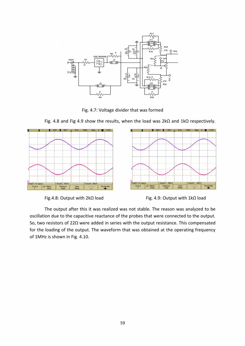
59
Fig. 4.7: Voltage divider that was formed
Fig. 4.8 and Fig 4.9 show the results, when the load was 2kΩ and 1kΩ respectively.
Fig.4.8: Output with 2kΩ load Fig. 4.9: Output with 1kΩ load
The output after this it was realized was not stable. The reason was analyzed to be
oscillation due to the capacitive reactance of the probes that were connected to the output.
So, two resistors of 22Ω were added in series with the output resistance. This compensated
for the loading of the output. The waveform that was obtained at the operating frequency
of 1MHz is shown in Fig. 4.10.
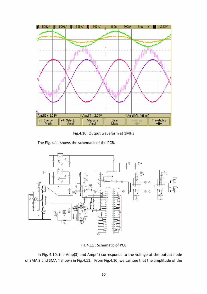
60
Fig.4.10: Output waveform at 1MHz
The Fig. 4.11 shows the schematic of the PCB.
Fig.4.11 : Schematic of PCB
In Fig. 4.10, the Amp(3) and Amp(4) corresponds to the voltage at the output node
of SMA 3 and SMA 4 shown in Fig.4.11. From Fig.4.10, we can see that the amplitude of the
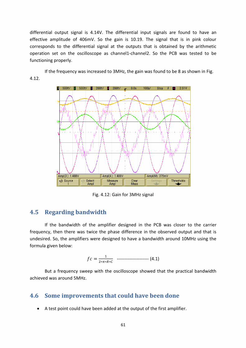
61
differential output signal is 4.14V. The differential input signals are found to have an
effective amplitude of 406mV. So the gain is 10.19. The signal that is in pink colour
corresponds to the differential signal at the outputs that is obtained by the arithmetic
operation set on the oscilloscope as channel1-channel2. So the PCB was tested to be
functioning properly.
If the frequency was increased to 3MHz, the gain was found to be 8 as shown in Fig.
4.12.
Fig. 4.12: Gain for 3MHz signal
4.5 Regarding bandwidth
If the bandwidth of the amplifier designed in the PCB was closer to the carrier
frequency, then there was twice the phase difference in the observed output and that is
undesired. So, the amplifiers were designed to have a bandwidth around 10MHz using the
formula given below:
--------------------- (4.1)
But a frequency sweep with the oscilloscope showed that the practical bandwidth
achieved was around 5MHz.
4.6 Some improvements that could have been done
A test point could have been added at the output of the first amplifier.
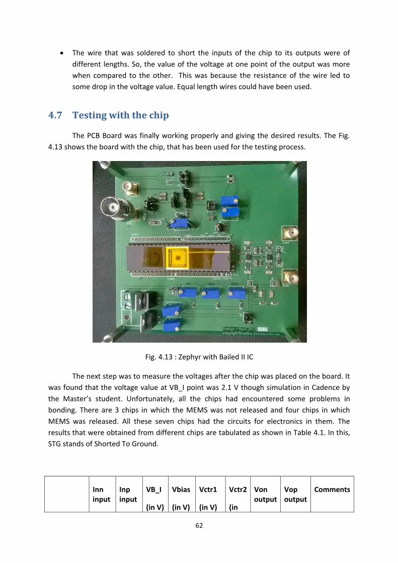
62
The wire that was soldered to short the inputs of the chip to its outputs were of
different lengths. So, the value of the voltage at one point of the output was more
when compared to the other. This was because the resistance of the wire led to
some drop in the voltage value. Equal length wires could have been used.
4.7 Testing with the chip
The PCB Board was finally working properly and giving the desired results. The Fig.
4.13 shows the board with the chip, that has been used for the testing process.
Fig. 4.13 : Zephyr with Bailed II IC
The next step was to measure the voltages after the chip was placed on the board. It
was found that the voltage value at VB_I point was 2.1 V though simulation in Cadence by
the Master’s student. Unfortunately, all the chips had encountered some problems in
bonding. There are 3 chips in which the MEMS was not released and four chips in which
MEMS was released. All these seven chips had the circuits for electronics in them. The
results that were obtained from different chips are tabulated as shown in Table 4.1. In this,
STG stands of Shorted To Ground.
Inn input
Inp input
VB_I
(in V)
Vbias
(in V)
Vctr1
(in V)
Vctr2
(in
Von output
Vop output
Comments
63
(in V) (in V) V)
(in V) (in V)
Unreleased chip I
1.04 1.04 0.1m 0.213 STG 0.4 STG 1.5 The power line is broken
Unreleased chip II
STG STG 2.1 0.613 0.4 0.4 STG 1.66 Could be repaired
Unreleased chip III
STG STG 2.1 0.6 0.4 0.4 STG 1.6 Could be repaired
Released MEMS I
STG STG 2.1 0.624 0.4 STG STG 1.5 Could be repaired
Released MEMS II
STG STG STG STG STG STG 0.122 STG Fused Powerline
Released MEMS III
1.04 1.04 STG 0.21 0.0122 0.4 STG STG Fused Powerline
Released MEMS IV
STG STG STG STG STG 0.4 STG 0.2 Fused Powerline
Table 4.1: Table showing the voltages after the chip was tested initially
4.8 Further work with this chip
The chips have to be re-packaged with proper bonding. Then, when these are tested,
proper results can be obtained. Another option would be to repair the chip by oneself and
check if the chip is working. This work is beyond the time frame allotted. So in the future,
these works with this chip and the PCB can be carried out.
4.9 Conclusion
This chapter has illustrated the working of the PCB and some measurements that
were done with the Bailed II IC chip.
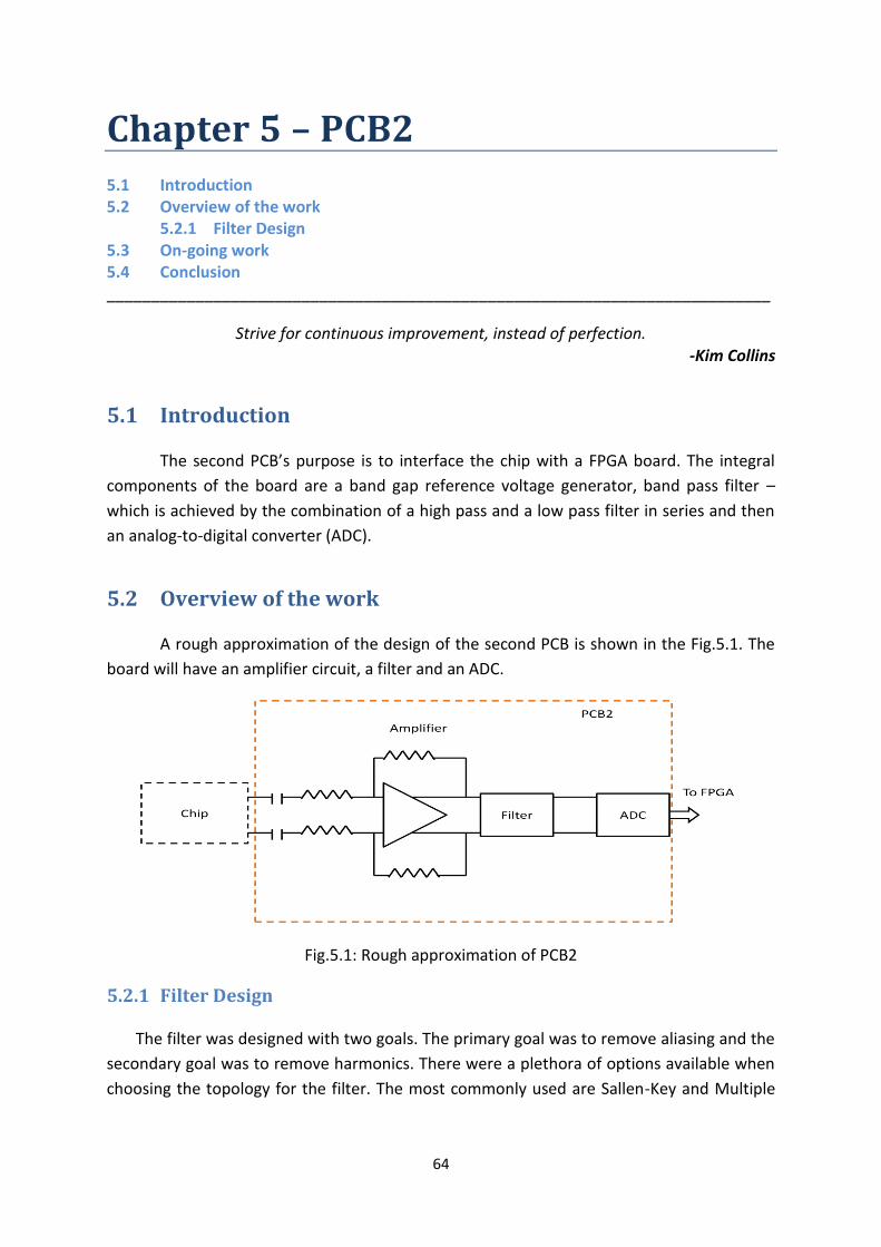
64
Chapter 5 – PCB2
5.1 Introduction 5.2 Overview of the work
5.2.1 Filter Design 5.3 On-going work 5.4 Conclusion ___________________________________________________________________________
Strive for continuous improvement, instead of perfection. -Kim Collins
5.1 Introduction
The second PCB’s purpose is to interface the chip with a FPGA board. The integral
components of the board are a band gap reference voltage generator, band pass filter –
which is achieved by the combination of a high pass and a low pass filter in series and then
an analog-to-digital converter (ADC).
5.2 Overview of the work
A rough approximation of the design of the second PCB is shown in the Fig.5.1. The
board will have an amplifier circuit, a filter and an ADC.
Fig.5.1: Rough approximation of PCB2
5.2.1 Filter Design
The filter was designed with two goals. The primary goal was to remove aliasing and the
secondary goal was to remove harmonics. There were a plethora of options available when
choosing the topology for the filter. The most commonly used are Sallen-Key and Multiple
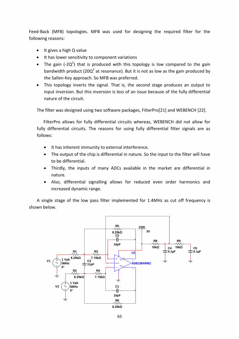
65
Feed-Back (MFB) topologies. MFB was used for designing the required filter for the
following reasons:
It gives a high Q value
It has lower sensitivity to component variations
The gain (-2Q2) that is produced with this topology is low compared to the gain
bandwidth product (20Q2 at resonance). But it is not as low as the gain produced by
the Sallen-Key approach. So MFB was preferred.
This topology inverts the signal. That is, the second stage produces an output to
input inversion. But this inversion is less of an issue because of the fully differential
nature of the circuit.
The filter was designed using two software packages, FilterPro[21] and WEBENCH [22].
FilterPro allows for fully differential circuits whereas, WEBENCH did not allow for
fully differential circuits. The reasons for using fully differential filter signals are as
follows:
It has inherent immunity to external interference.
The output of the chip is differential in nature. So the input to the filter will have
to be differential.
Thirdly, the inputs of many ADCs available in the market are differential in
nature.
Also, differential signalling allows for reduced even order harmonics and
increased dynamic range.
A single stage of the low pass filter implemented for 1.4MHz as cut off frequency is
shown below.
R1
8.25kΩ
R2
8.25kΩ
R3
7.15kΩ
R4
7.15kΩ
R5
8.25kΩ
R6
8.25kΩ
C1
10pF
C2
10pF
C311pF
V1 1 Vpk
5MHz
0°
V21 Vpk
5MHz
0°
U1
AD8138ARMZVocm
Out-
Out+
8
1
2
3
6
5
4
VDD
3V
R8
10kΩ
R9
10kΩC40.1µF
C50.1µF

66
Fig.5.2: MFB low pass filter for 1.4MHz cut off frequency
This filter can be designed for any other cut off frequency using the same position of
components and just changing the values of resistors and capacitors. A Butterworth
filter design was chosen to implement the design in the FilterPro software. Butterworth
was chosen over Chebyshev filter because it is maximally flat filter with moderate
overshoot and ringing. Also, the pulse response is better than the Chebyshev filter.
5.3 Ongoing work
A high pass filter for the stage before the low pass filter is being designed. Also a
suitable ADC that can be used for the stage after the filtering process is looked into. Another
IC that is being searched for is, an appropriate voltage reference IC.
5.4 Conclusion
This chapter illustrates the work completed for the second PCB. Owing to time
constrains, the work for PCB2 will be continued as far as possible after the presentation
date.

67
Chapter 6 - Conclusion
The project work involved the following activities:
The design of the PCB
The different modules were designed for the required functionality.
Implementation of the design
After the PCB was manufactured, the components were bought from Farnell
Electronics and they were soldered.
Verification
The PCB was verified for correct functionality. Also tests were carried out
with the chip
Further work was carried out in the form of repairing of the bound wires in the chip.
This has made one chip work and the primary results of its working will be presented in the
oral presentation.

68
Bibliography
[1] Toshifumi Konishi, Daisuke Yamane, Takaaki Matsushima, Kazuya Masu, Katsuyuki Machida, and Hiroshi Toshiyoshi (2014) 'A capacitive CMOS–MEMS sensor designed by multi-physics simulation for integrated CMOS–MEMS technology', Japanese Journal of Applied Physics, 53(04EE15), pp. [Online]. Available at:http://iopscience.iop.org/1347-4065/53/4S/04EE15 (Accessed: 22nd February 2014). [2]Dimension Engineering LLC A beginner’s guide to accelerometers, Available at:https://www.dimensionengineering.com/info/accelerometers (Accessed: 25th February 2014). [3]Joel Voldman, course materials for 6.777J / 2.372J Design and Fabrication ofMicroelectromechanicalDevices, Spring 2007. MIT OpenCourseWare(http://ocw.mit.edu/), Massachusetts Institute of Technology. Downloaded on 23 May 2014. JV: 2.372J/6.777J Spring 2007, Lecture 24 -5 [4] A. Witvrouw et al., Microsys. Tech., 6(5), pp. 192-199, 2000. [5] A. Witvrouw et al., MRS Proc. 782, pp. 25-36, 2004. [6] C. Van Hoof et al., Science 304, pp. 986-987, 2004. [7] R. Howe et al., MRS Proc. 729, pp. 205-231, 2003. [8] Witvrouw, A., "CMOS-MEMS Integration: Why, How and What?," Computer-Aided Design, 2006. ICCAD '06. IEEE/ACM International Conference on , vol., no., pp.826,827, 5-9 Nov. 2006 doi: 10.1109/ICCAD.2006.320128 [8] Piotr Michalik, Daniel Fernández, Jordi Madrenas, Mehmet Kaynak, Matthias Wietstruck, “An approach to MEMS smart sensor design using CMOS BEOL“,MEMSWAVE 2013, Available at: http://www.ihp-microelectronics.com/en/infocenter/events/archive/presentations-2013.html (Accessed: 12th May 2014). [9] Michalik, P.; Madrenas, J.; Fernandez, D., "Sense/drive architecture for CMOS-MEMS accelerometers with relaxation oscillator and TDC," Electronics, Circuits and Systems (ICECS), 2012 19th IEEE International Conference on , vol., no., pp.937,940, 9-12 Dec. 2012 doi: 10.1109/ICECS.2012.6463507 [10] http://en.wikipedia.org/wiki/Schematic_capture [11] http://www.geda-project.org/ [12] http://www.gpleda.org/ [13] www.linear.com/product/LT1763 [14] www.linear.com/product/LT1761 [15] http://www.ti.com/product/lm4132 [16] http://www.alldatasheet.com/datasheet-pdf/pdf/128023/ONSEMI/LM317BTG.html [17] http://www.mouser.cn/ProductDetail/ECS/LTE45MB/?qs=PxiiilAMTltudXfFp7Ke3A== [18] http://www.farnell.com/datasheets/1303882.pdf [19] www.analog.com/static/imported-files/data_sheets/AD8138.pdf [20] PCB Design Tutorial by David L. Jones ; Revision A - June 29th 2004; The latest version of this tutorial can be found through www.alternatezone.com [21] http://www.ti.com/tool/filterpro [22] http://www.ti.com/lsds/ti/analog/webench/webench-filters.page [23] www.qub.ac.uk/cite2write/harvard3l.html


![Universitat Politècnica de València Universitat Politècnica de València · 2014. 8. 8. · [2014/7056] RESOLUCIÓN de 22 de julio de 2014, de la Universitat Politècnica de València,](https://img.pdfslide.net/doc/110x75/60bcc72398a71848640018dc/universitat-politcnica-de-valncia-universitat-politcnica-de-val-2014-8.jpg)