Embed Size (px)
Citation preview
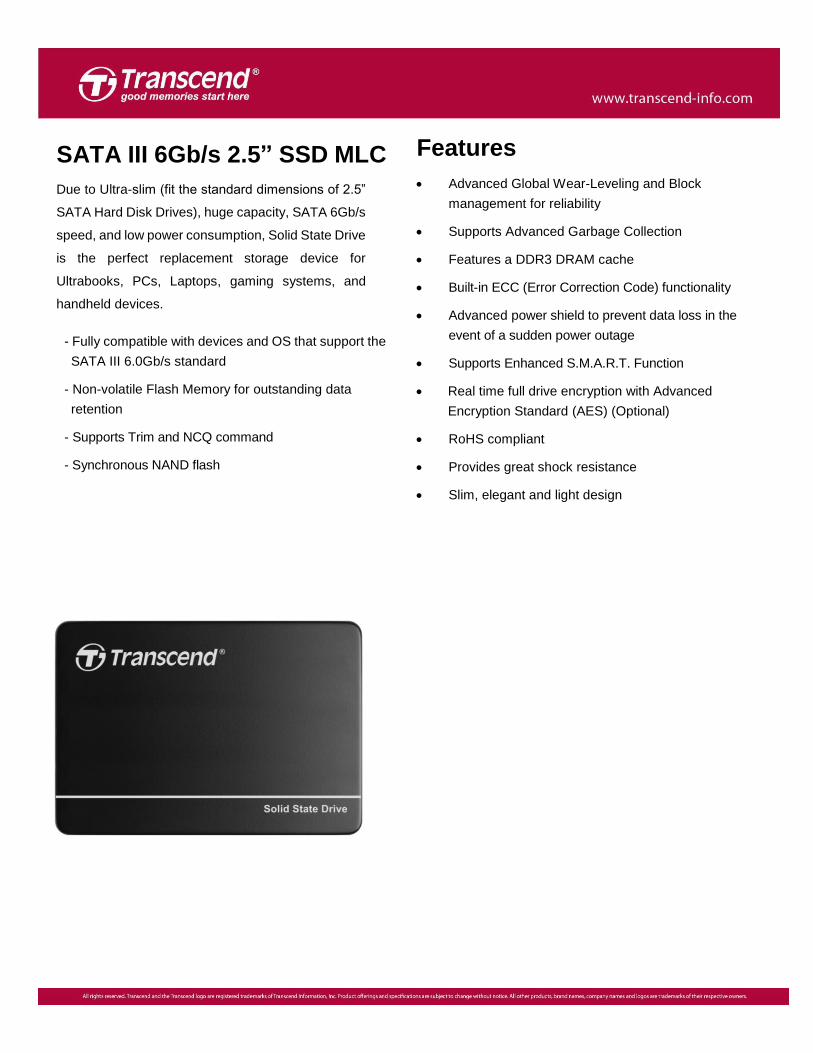
SATA III 6Gb/s 2.5” SSD MLC
Due to Ultra-slim (fit the standard dimensions of 2.5”
SATA Hard Disk Drives), huge capacity, SATA 6Gb/s
speed, and low power consumption, Solid State Drive
is the perfect replacement storage device for
Ultrabooks, PCs, Laptops, gaming systems, and
handheld devices.
- Fully compatible with devices and OS that support the
SATA III 6.0Gb/s standard
- Non-volatile Flash Memory for outstanding data
retention
- Supports Trim and NCQ command
- Synchronous NAND flash
Features
Advanced Global Wear-Leveling and Block
management for reliability
Supports Advanced Garbage Collection
Features a DDR3 DRAM cache
Built-in ECC (Error Correction Code) functionality
Advanced power shield to prevent data loss in the
event of a sudden power outage
Supports Enhanced S.M.A.R.T. Function
Real time full drive encryption with Advanced
Encryption Standard (AES) (Optional)
RoHS compliant
Provides great shock resistance
Slim, elegant and light design

Specifications
Performance
Model P/N
ATTO CrystalDiskMark IOmeter
Max. Read
*
Max. Write
*
Sequential Read
**
Sequential Write
**
Random Read
(4KB QD32) **
Random Write
(4KB QD32) **
IOPS Random
Read (4KB QD32)
***
IOPS Random
Write (4KB QD32)
***
TS32ASTMM0000A 280 55 280 55 110 55 26K 13K
TS64ASTMM0000A 560 110 520 100 210 100 50K 25K
TS128ASTMM0000A 570 210 530 210 290 210 70K 50K
TS256ASTMM0000A 570 400 530 400 300 330 75K 75K
TS512ASTMM0000A 570 470 530 470 300 320 75K 75K
TS000ASTMM0000A 570 470 530 470 300 320 75K 75K
Note: Maximum transfer speed recorded
* 25 oC, test on ASUS P8Z68-M PRO, 4 GB, Windows
® 7 Professional with AHCI mode, benchmark utility ATTO (version 2.41), unit MB/s
** 25 oC, test on ASUS P8Z68-M PRO, 4 GB, Windows
® 7 Professional with AHCI mode, benchmark utility CrystalDiskMark (version 3.0.1),
copied file 1000MB, unit MB/s *** 25
oC, test on ASUS P8Z68-M PRO, 4 GB, Windows
® 7 Professional with AHCI mode, benchmark utility IOmeter2006 with 4K file size and queue
depth of 32, unit IOPs
**** The recorded performance is obtained while the SSD is not operating as an OS disk
Physical Specification
Form Factor 2.5 inch HDD
Storage Capacities 32 GB to 1TB
Dimensions
Length 99.80 0.25 mm 3.929 0.01 inch
Width 69.80 0.25 mm 2.748 0.01 inch
Height 7.00 0.3 mm 0.276 0.012 inch
Input Voltage 5V 5%
Weight 52 2 g
Connector SATA 22 pins connector
Environmental Specifications
Operating Temperature 10 oC to 80
oC
Storage Temperature 40 oC to 85
oC
Humidity Operating 0 % to 95 % (Non-condensing)
Non-Operating 0 % to 95 % (Non-condensing)
*Tested with IOmeter running sequential reads/writes and idle mode
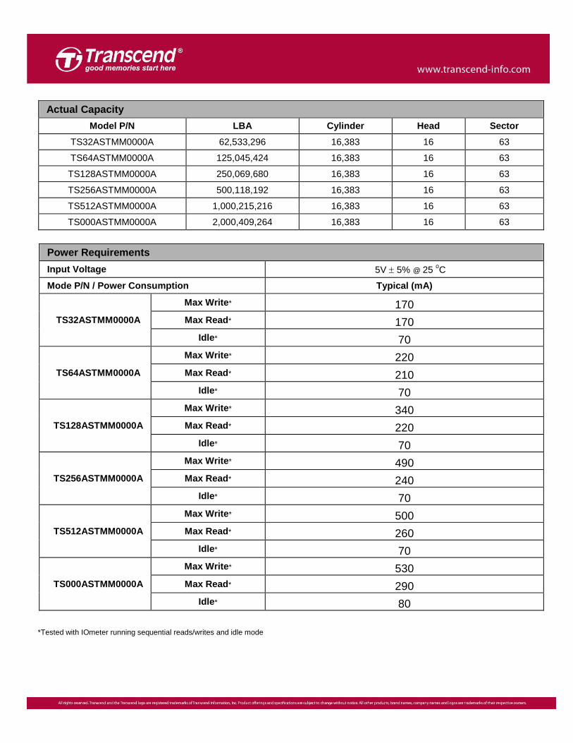
Power Requirements
Input Voltage 5V 5% @ 25 oC
Mode P/N / Power Consumption Typical (mA)
TS32ASTMM0000A
Max Write* 170
Max Read* 170
Idle* 70
TS64ASTMM0000A
Max Write* 220
Max Read* 210
Idle* 70
TS128ASTMM0000A
Max Write* 340
Max Read* 220
Idle* 70
TS256ASTMM0000A
Max Write* 490
Max Read* 240
Idle* 70
TS512ASTMM0000A
Max Write* 500
Max Read* 260
Idle* 70
TS000ASTMM0000A
Max Write* 530
Max Read* 290
Idle* 80
Actual Capacity
Model P/N LBA Cylinder Head Sector
TS32ASTMM0000A 62,533,296 16,383 16 63
TS64ASTMM0000A 125,045,424 16,383 16 63
TS128ASTMM0000A 250,069,680 16,383 16 63
TS256ASTMM0000A 500,118,192 16,383 16 63
TS512ASTMM0000A 1,000,215,216 16,383 16 63
TS000ASTMM0000A 2,000,409,264 16,383 16 63
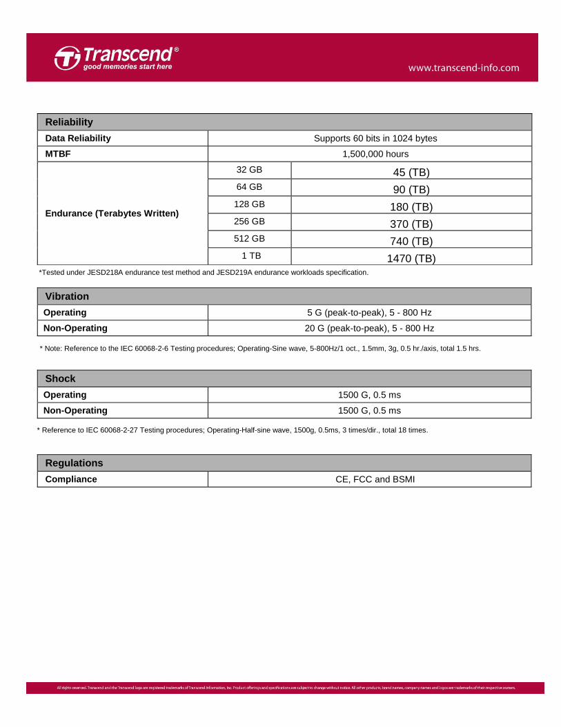
*Tested under JESD218A endurance test method and JESD219A endurance workloads specification.
* Note: Reference to the IEC 60068-2-6 Testing procedures; Operating-Sine wave, 5-800Hz/1 oct., 1.5mm, 3g, 0.5 hr./axis, total 1.5 hrs.
* Reference to IEC 60068-2-27 Testing procedures; Operating-Half-sine wave, 1500g, 0.5ms, 3 times/dir., total 18 times.
Reliability
Data Reliability Supports 60 bits in 1024 bytes
MTBF 1,500,000 hours
Endurance (Terabytes Written)
32 GB 45 (TB)
64 GB 90 (TB)
128 GB 180 (TB)
256 GB 370 (TB)
512 GB 740 (TB)
1 TB 1470 (TB)
Vibration
Operating 5 G (peak-to-peak), 5 - 800 Hz
Non-Operating 20 G (peak-to-peak), 5 - 800 Hz
Shock
Operating 1500 G, 0.5 ms
Non-Operating 1500 G, 0.5 ms
Regulations
Compliance CE, FCC and BSMI
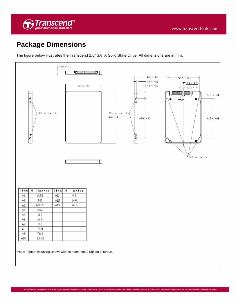
Package Dimensions
The figure below illustrates the Transcend 2.5” SATA Solid State Drive. All dimensions are in mm.
*Note: Tighten mounting screws with no more than 2 Kgf-cm of torque.
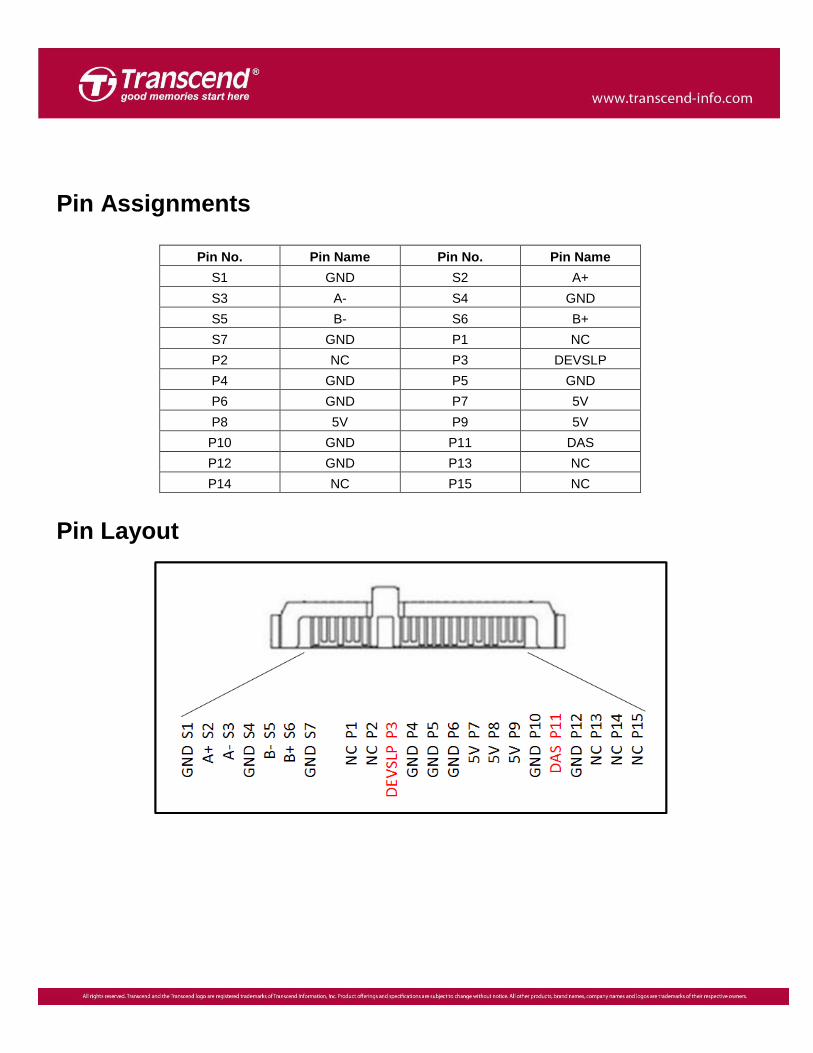
Pin Assignments
Pin No. Pin Name Pin No. Pin Name
S1 GND S2 A+
S3 A- S4 GND
S5 B- S6 B+
S7 GND P1 NC
P2 NC P3 DEVSLP
P4 GND P5 GND
P6 GND P7 5V
P8 5V P9 5V
P10 GND P11 DAS
P12 GND P13 NC
P14 NC P15 NC
Pin Layout
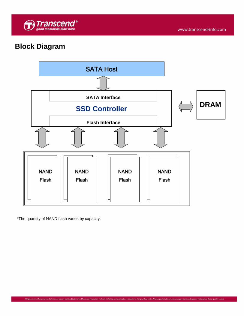
Block Diagram
*The quantity of NAND flash varies by capacity.
SATA Host
SSD Controller
Flash Interface
SATA Interface
NAND
Flash
NAND
Flash
NAND
Flash
DRAM
NAND
Flash
Features
Wear-Leveling algorithm
The controller supports static/dynamic wear leveling. When the host writes data, the controller will find and use the block
with the lowest erase count among the free blocks. This is known as dynamic wear leveling. When the free blocks ‘erase
count is higher than the data blocks’, it will activate the static wear leveling, replacing the not so frequently used user
blocks with the high erase count free blocks.
Bad-block management
When the flash encounters ECC fail, program fail or erase fail, the controller will mark the block as bad block to prevent
using this block and cause data loss in the future.
Enhanced S.M.A.R.T. function
Transcend’s SSDs support the innovative S.M.A.R.T. command (Self-Monitoring, Analysis, and Reporting Technology)
that allows the users to evaluate the health information of their SSD in an efficient way.
StaticDataRefresh Technology
Normally, ECC engine corrections are taken place without affecting the host normal operations. As time passes by, the
number of error bits accumulated in the read transaction exceeds the correcting capability of the ECC engine, resulting in
corrupted data being sent to the host. To prevent this, the controller monitors the error bit levels at each read operation;
when it reaches the preset threshold value, the controller automatically performs data refresh to “restore” the correct
charge levels in the cell. This implementation practically restores the data to its original, error-free state, and hence,
lengthening the life of the data.
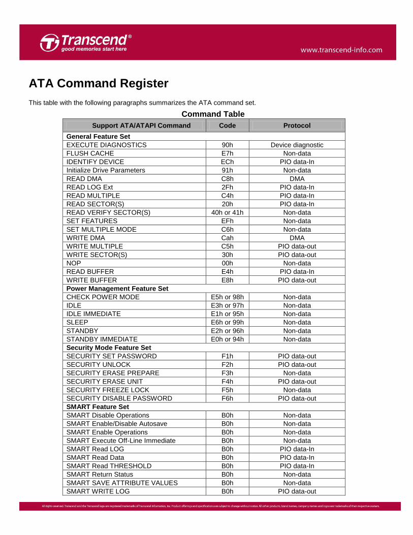
ATA Command Register
This table with the following paragraphs summarizes the ATA command set.
Command Table
Support ATA/ATAPI Command Code Protocol
General Feature Set
EXECUTE DIAGNOSTICS 90h Device diagnostic
FLUSH CACHE E7h Non-data
IDENTIFY DEVICE ECh PIO data-In
Initialize Drive Parameters 91h Non-data
READ DMA C8h DMA
READ LOG Ext 2Fh PIO data-In
READ MULTIPLE C4h PIO data-In
READ SECTOR(S) 20h PIO data-In
READ VERIFY SECTOR(S) 40h or 41h Non-data
SET FEATURES EFh Non-data
SET MULTIPLE MODE C6h Non-data
WRITE DMA Cah DMA
WRITE MULTIPLE C5h PIO data-out
WRITE SECTOR(S) 30h PIO data-out
NOP 00h Non-data
READ BUFFER E4h PIO data-In
WRITE BUFFER E8h PIO data-out
Power Management Feature Set
CHECK POWER MODE E5h or 98h Non-data
IDLE E3h or 97h Non-data
IDLE IMMEDIATE E1h or 95h Non-data
SLEEP E6h or 99h Non-data
STANDBY E2h or 96h Non-data
STANDBY IMMEDIATE E0h or 94h Non-data
Security Mode Feature Set
SECURITY SET PASSWORD F1h PIO data-out
SECURITY UNLOCK F2h PIO data-out
SECURITY ERASE PREPARE F3h Non-data
SECURITY ERASE UNIT F4h PIO data-out
SECURITY FREEZE LOCK F5h Non-data
SECURITY DISABLE PASSWORD F6h PIO data-out
SMART Feature Set
SMART Disable Operations B0h Non-data
SMART Enable/Disable Autosave B0h Non-data
SMART Enable Operations B0h Non-data
SMART Execute Off-Line Immediate B0h Non-data
SMART Read LOG B0h PIO data-In
SMART Read Data B0h PIO data-In
SMART Read THRESHOLD B0h PIO data-In
SMART Return Status B0h Non-data
SMART SAVE ATTRIBUTE VALUES B0h Non-data
SMART WRITE LOG B0h PIO data-out
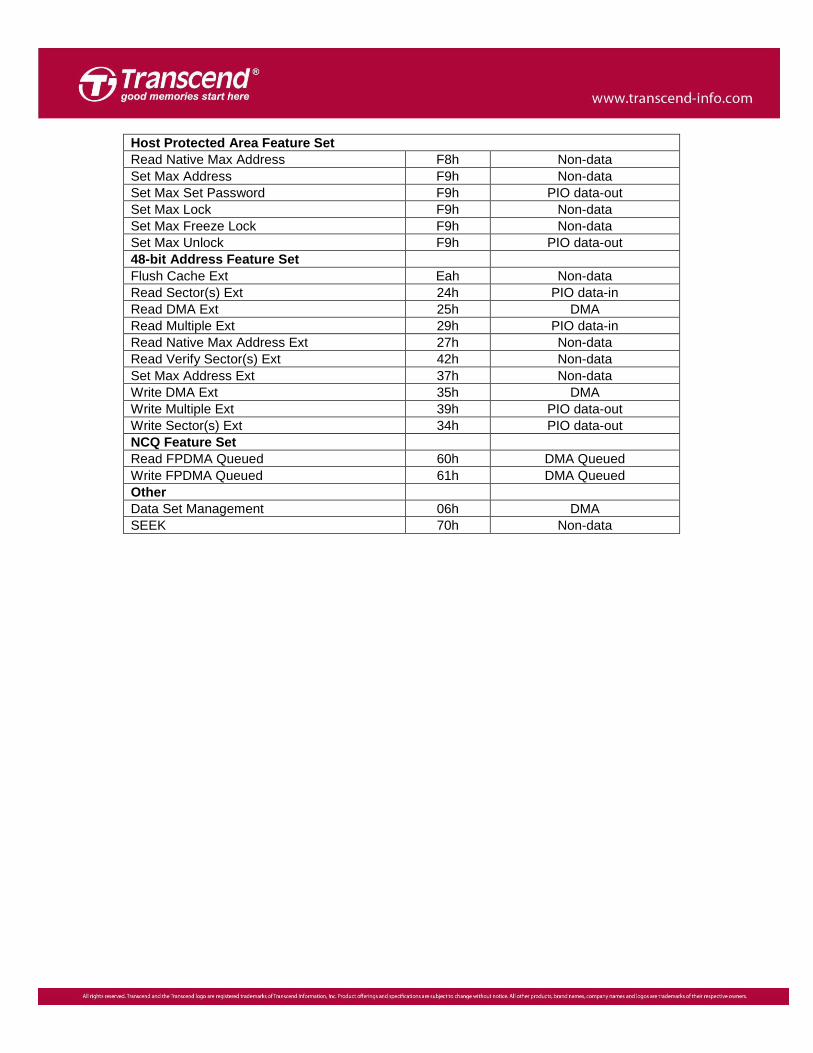
Host Protected Area Feature Set
Read Native Max Address F8h Non-data
Set Max Address F9h Non-data
Set Max Set Password F9h PIO data-out
Set Max Lock F9h Non-data
Set Max Freeze Lock F9h Non-data
Set Max Unlock F9h PIO data-out
48-bit Address Feature Set
Flush Cache Ext Eah Non-data
Read Sector(s) Ext 24h PIO data-in
Read DMA Ext 25h DMA
Read Multiple Ext 29h PIO data-in
Read Native Max Address Ext 27h Non-data
Read Verify Sector(s) Ext 42h Non-data
Set Max Address Ext 37h Non-data
Write DMA Ext 35h DMA
Write Multiple Ext 39h PIO data-out
Write Sector(s) Ext 34h PIO data-out
NCQ Feature Set
Read FPDMA Queued 60h DMA Queued
Write FPDMA Queued 61h DMA Queued
Other
Data Set Management 06h DMA
SEEK 70h Non-data
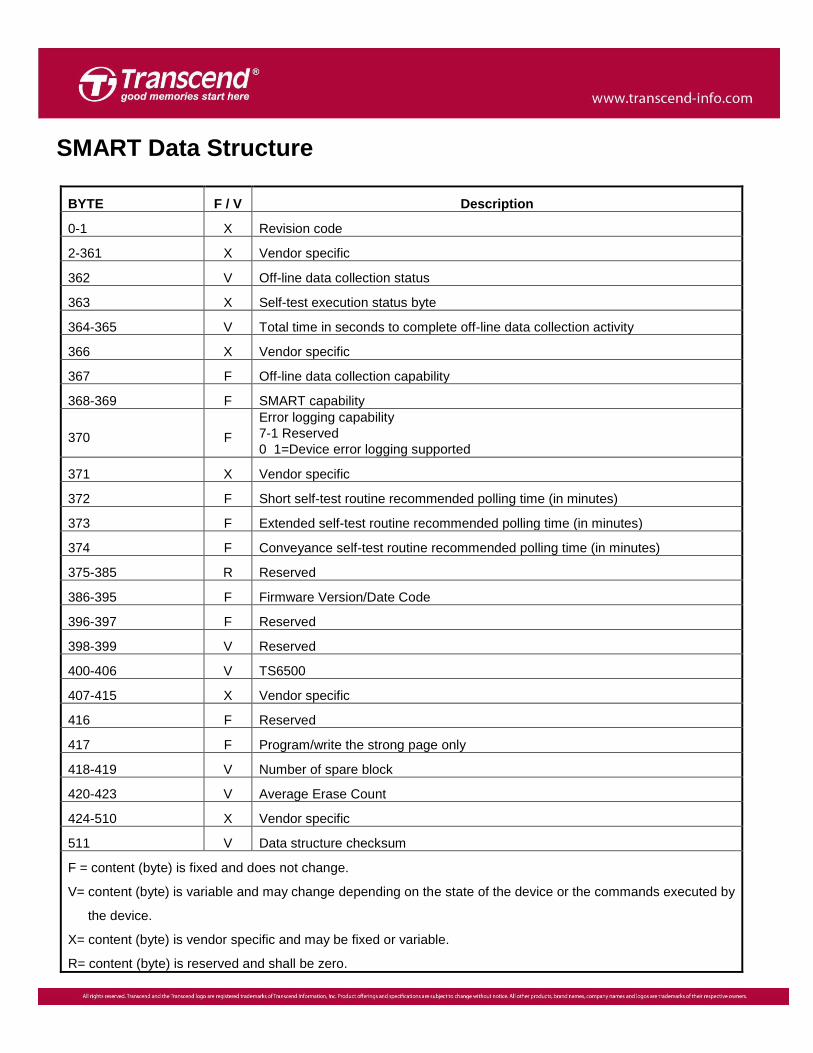
SMART Data Structure
BYTE F / V Description
0-1 X Revision code
2-361 X Vendor specific
362 V Off-line data collection status
363 X Self-test execution status byte
364-365 V Total time in seconds to complete off-line data collection activity
366 X Vendor specific
367 F Off-line data collection capability
368-369 F SMART capability
370 F
Error logging capability
7-1 Reserved
0 1=Device error logging supported
371 X Vendor specific
372 F Short self-test routine recommended polling time (in minutes)
373 F Extended self-test routine recommended polling time (in minutes)
374 F Conveyance self-test routine recommended polling time (in minutes)
375-385 R Reserved
386-395 F Firmware Version/Date Code
396-397 F Reserved
398-399 V Reserved
400-406 V TS6500
407-415 X Vendor specific
416 F Reserved
417 F Program/write the strong page only
418-419 V Number of spare block
420-423 V Average Erase Count
424-510 X Vendor specific
511 V Data structure checksum
F = content (byte) is fixed and does not change.
V= content (byte) is variable and may change depending on the state of the device or the commands executed by
the device.
X= content (byte) is vendor specific and may be fixed or variable.
R= content (byte) is reserved and shall be zero.
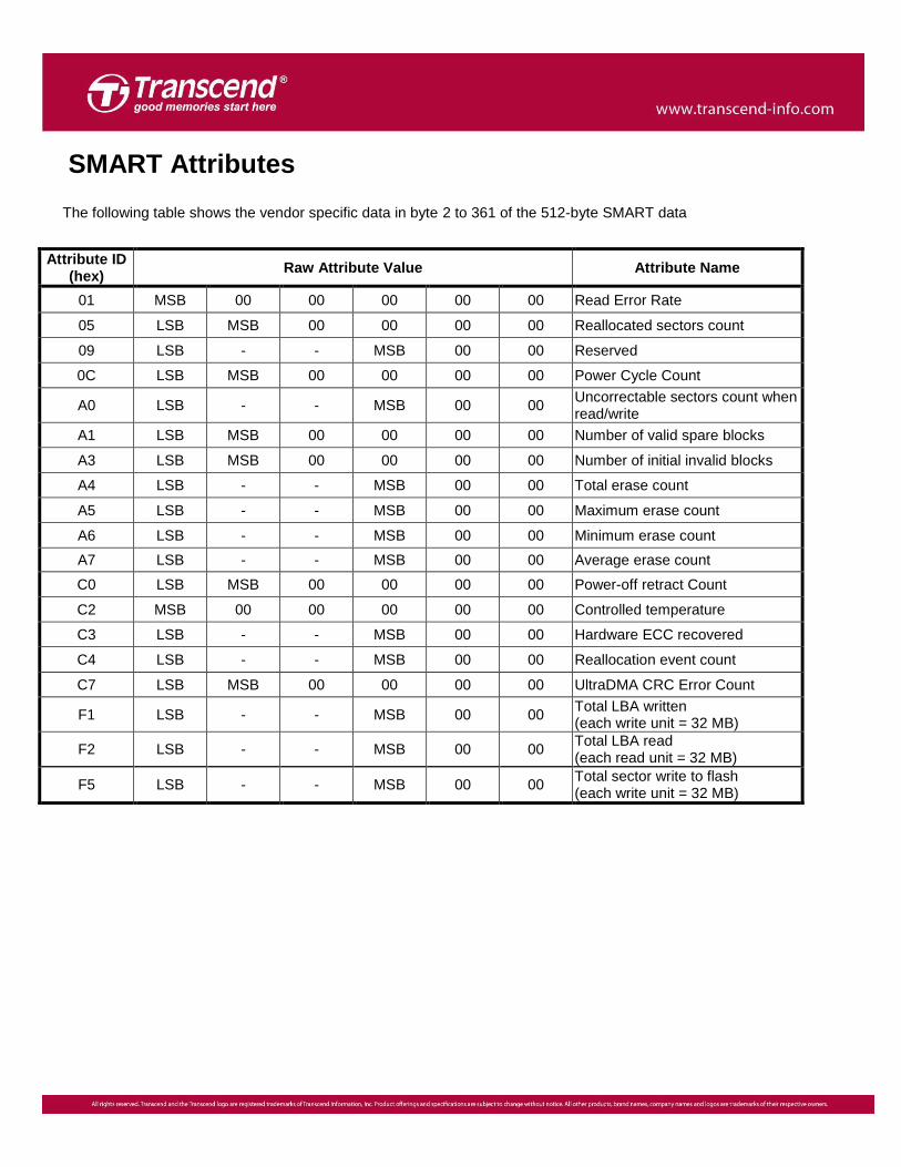
SMART Attributes
The following table shows the vendor specific data in byte 2 to 361 of the 512-byte SMART data
Attribute ID (hex)
Raw Attribute Value Attribute Name
01 MSB 00 00 00 00 00 Read Error Rate
05 LSB MSB 00 00 00 00 Reallocated sectors count
09 LSB - - MSB 00 00 Reserved
0C LSB MSB 00 00 00 00 Power Cycle Count
A0 LSB - - MSB 00 00 Uncorrectable sectors count when read/write
A1 LSB MSB 00 00 00 00 Number of valid spare blocks
A3 LSB MSB 00 00 00 00 Number of initial invalid blocks
A4 LSB - - MSB 00 00 Total erase count
A5 LSB - - MSB 00 00 Maximum erase count
A6 LSB - - MSB 00 00 Minimum erase count
A7 LSB - - MSB 00 00 Average erase count
C0 LSB MSB 00 00 00 00 Power-off retract Count
C2 MSB 00 00 00 00 00 Controlled temperature
C3 LSB - - MSB 00 00 Hardware ECC recovered
C4 LSB - - MSB 00 00 Reallocation event count
C7 LSB MSB 00 00 00 00 UltraDMA CRC Error Count
F1 LSB - - MSB 00 00 Total LBA written (each write unit = 32 MB)
F2 LSB - - MSB 00 00 Total LBA read (each read unit = 32 MB)
F5 LSB - - MSB 00 00 Total sector write to flash (each write unit = 32 MB)
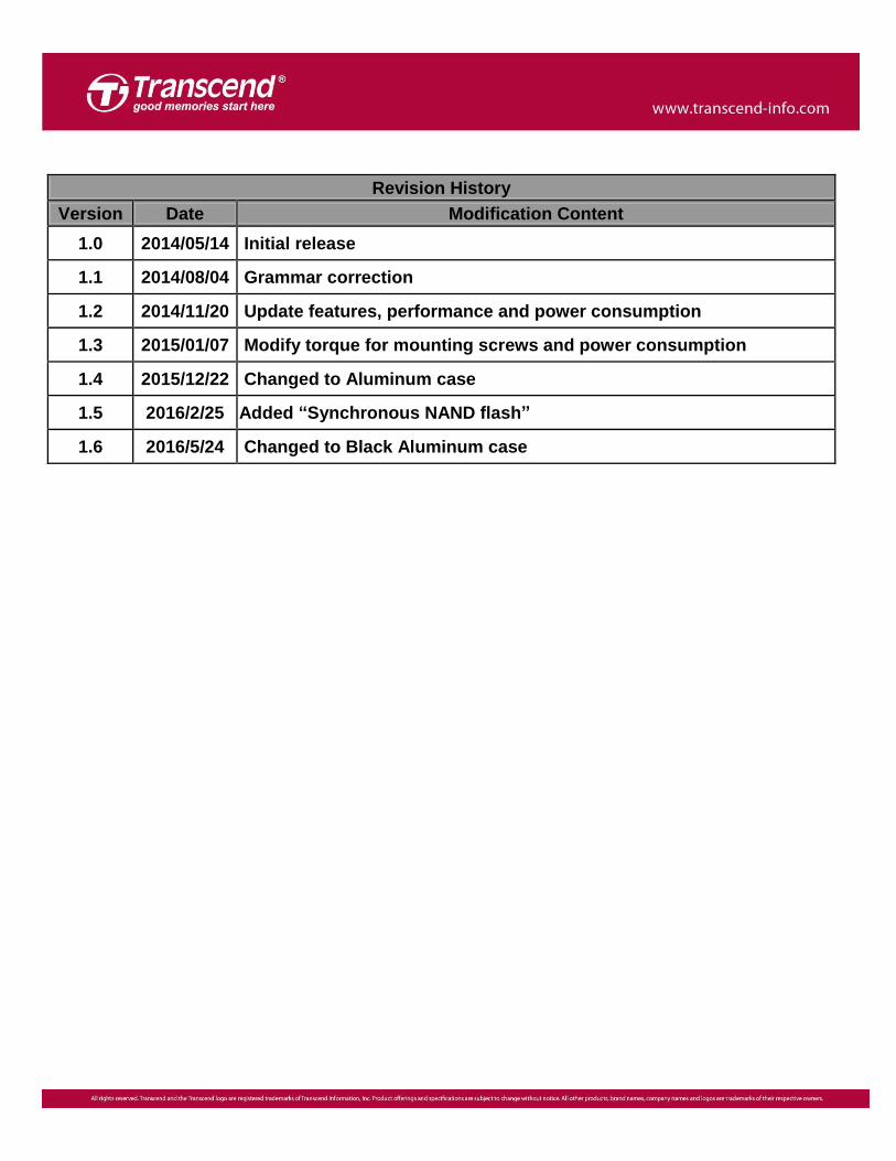
Revision History
Version Date Modification Content
1.0 2014/05/14 Initial release
1.1 2014/08/04 Grammar correction
1.2 2014/11/20 Update features, performance and power consumption
1.3 2015/01/07 Modify torque for mounting screws and power consumption
1.4 2015/12/22 Changed to Aluminum case
1.5 2016/2/25 Added “Synchronous NAND flash”
1.6 2016/5/24 Changed to Black Aluminum case