Embed Size (px)
Citation preview
SOME ASPECTS ON INTEGRATED CURRENT SHUNTS FOR HIGH FREQUENCY SWITCHING POWER ELECTRONIC CONVERTERS A.L.J. Joannou* D.C. Pentz* J.D. van Wyk* * Group on Electronic Energy Processing (GEEP), Dept. of Electrical and Electronic Engineering Science, Corner of University Road and Kingsway Road, University of Johannesburg, Johannesburg 2006, South Africa E-mail: [email protected] Abstract: Switched power electronic converters are now able to operate at very high frequencies due to the development in wide band gap high electron mobility transistors (HEMT) such as GaN and SiC power semi-conductor technologies. Measuring current at such high switching frequencies with rise and fall times of a few nanoseconds, requires specialised instruments and a good knowledge of measurement techniques. Current measurement technologies that are readily available are relatively expensive and can add unwanted parasitic impedances to the circuit. This paper investigates some aspects for a few current shunt options that can be integrated into a converter. Keywords: Current measurement, high frequency, current shunt.
1 INTRODUCTION The drive for smaller power electronic converters with a higher power density and high efficiency has forced the operating frequencies of converters to increase. The well-known advantage of the increase in switching frequency is that the energy storage elements reduce in magnitude and in essence physical size. Although size limitations still exist due to the magnetic energy storage elements, the overall reduction is still considerable. In the past, the limitation of the maximum switching frequency of these converters was the transistor losses associated with slow switching transients. With recent developments in wide band gap power semi-conductor technology, this is no longer the case. Two of the most recent power semi-conductor technologies are Silicon Carbide (SiC) and Gallium Nitride (GaN) [1]. These wide band gap semi-conductors are power switching transistors which are theoretically able to switch at frequencies previously not achievable by Silicon (Si) devices [2]. They also have a higher power density compared to conventional silicon based semi-conductors [2]. The GaN transistors are said to be able to achieve even better characteristics than the SiC devices as discussed in [2] and [1]. These types of semi-conductor switches can now make the high frequency hard switching power electronic converters possible. This leaves power measurement of these high frequency converters as a potential problem. Although actual measurement probes are well developed, especially for voltage measurement, the high frequency switching operation of the circuit can cause stray flux to couple onto the measurement leads, causing considerable measurement error [3]. Voltage measurement terminals can be integrated into the main power circuit PCB which reduce the inductance of the measurement probe and hence the error for voltage measurements. Therefore HF switching voltage measurement can be performed
accurately. For sufficient power measurements, current also needs to be measured accurately. Current measurement in power converters is well established, but these are bandwidth limited, have a response time delay and can become complex for high frequency accuracy and hence sensitive to interference. Current probes and a few other methods require that a loop be added to accommodate the current measurement device. This loop adds inductance to the circuit which will change the operating characteristics of the circuit. For this reason current probes and electromagnetic field based current measurement methods as in [4], [5]and [6] (e.g. hall-effect or Rogowski coils) are not discussed in this paper. The interest of this paper is mainly resistive shunts and in-circuit current measurement. Ideally high frequency switching power electronic circuits should have as little parasitic inductance and capacitance as possible. This implies that current and voltage sensors should be carefully designed and characterised to ensure that the parasitic impedance they add is negligible whilst still maintaining accuracy in the measurement. This is especially important for new switching devices such as eGaN FETs [4].
2 CURRENT MEASUREMENT IN POWER ELECTRONIC CONVERTERS
Measuring current in power electronic circuits is important for several reasons, such as protection and control. Measuring current in RF devices in the past was not a concern, since the devices were either low power, or operated under sinusoidal conditions. Measuring the pulsed current waveforms in power electronic circuits requires current sensors with high bandwidth capability. The bandwidth of any device corresponds to the 3dB knee frequency which also correlates to a 45 degree phase shift at that 3dB point. This large phase shift can cause inaccurate measurement and possibly failure in the
circuit. This is why it is important to realise that measurement specifications for non-sinusoidal switching power electronic circuits must be strict and that the 3dB rated frequency is not a true or sufficient figure of merit for comparison. Current sensors, specifically in power electronic circuits, aim to achieve the following characteristics as listed in [5]: • Compact size with a very low profile • Ease of manufacture and low cost • High bandwidth for high frequency operation • Fast response with small/few or no parasitic elements
introduced • Reliable with good noise immunity • High stability with varying temperature The criteria listed above are used as guidelines while investigating the integrated current shunts discussed in this paper. The accuracy of a current sensor relies heavily on the impedance matching of the input and outputs of the device under test [6]. The possible voltage response which can be measured across the shunt will reveal characteristics of the shunt as well as the circuit in which the shunt is placed. Three main effects are: 1. Slow rise time will be due to inductance added by the
shunt (or circuit inductance). Any stray circuit capacitance will then cause ringing and result in an overshoot
2. Skin effect will cause the initial voltage measured across the shunt to be higher, and once the current density is uniform, the voltage across the shunt will decrease reach a true steady state value
3. Coupling effects in the measurement if the measurement probe is not placed in a “field free” region.
Three different current shunt technologies are discussed next. These are single resistor current shunt, the lateral current shunt as well as the co-axial current shunt.
3 INTEGRATED CURRENT SHUNT MEASUREMENT DEVICES
It is again noted that the focus of this paper is specifically on current shunt measurement. Thus only shunts are considered. The shunts that are discussed in this paper are for low current applications (below 20 amperes). This low current will correspond to the voltage drop across the shunt resistor being comparable with the leakage flux that could induce measurement noise. Thus the shunt needs to be designed such that the desired signal can be differentiated from the measurement error.
3.1 Single surface mount (SMD) resistor measurement
The DC output current of power electronic converters is often measured by using a single SMD resistor as a current shunt. Using a single resistor as a shunt to
measure high frequency switching current will not yield an accurate representation of the actual current.
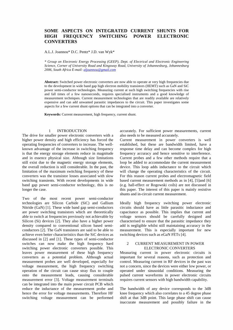
Figure 1: Single SMD resistor current shunt
The environment associated with the single resistor shunt falsifies the measurement. This is because the resistor can be physically small thus allowing one to neglect the electric energy stored, but the magnetic energy stored cannot be neglected because it can also not be defined. The magnetic energy is highly dependent on the associated surroundings of the resistor, how high it is from the PCB and components in close proximity to the resistor. These will all affect the magnetic energy around the resistor. Therefore the reliability of this type of shunt is expected to be low.
3.2 Lateral Shunt
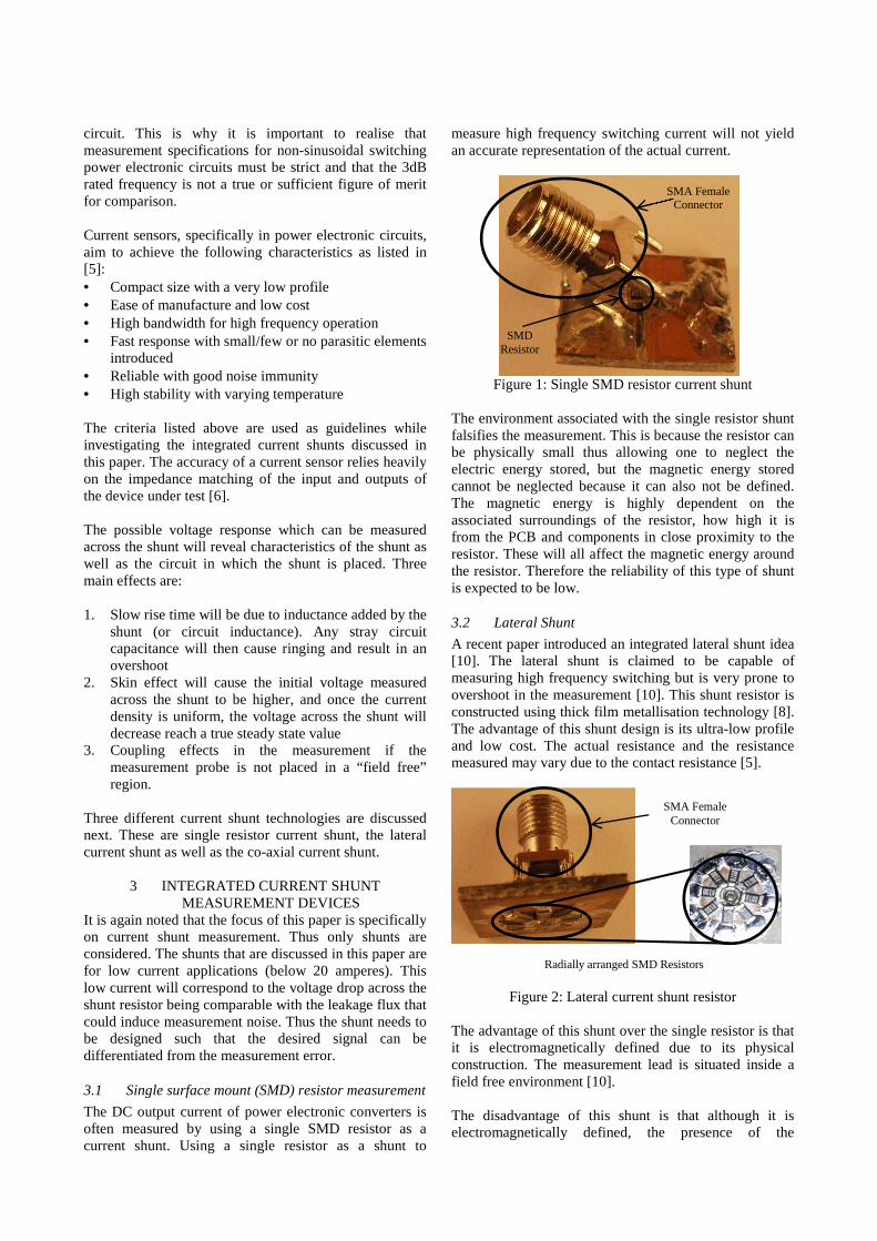
A recent paper introduced an integrated lateral shunt idea [10]. The lateral shunt is claimed to be capable of measuring high frequency switching but is very prone to overshoot in the measurement [10]. This shunt resistor is constructed using thick film metallisation technology [8]. The advantage of this shunt design is its ultra-low profile and low cost. The actual resistance and the resistance measured may vary due to the contact resistance [5].
Figure 2: Lateral current shunt resistor
The advantage of this shunt over the single resistor is that it is electromagnetically defined due to its physical construction. The measurement lead is situated inside a field free environment [10]. The disadvantage of this shunt is that although it is electromagnetically defined, the presence of the
SMD Resistor
SMA Female Connector
SMA Female Connector
Radially arranged SMD Resistors
electromagnetic stored energy of the shunt still obscures the measurement. The shunt physically resembles a capacitor and will therefore store a large amount of electric energy. This shunt will also experience time dependent conduction effects. This will greatly affect the wave shape of the measured voltage across the shunt. The way in which the current flows and stabilises itself uniformly through the shunt will affect the measured voltage. The current flows from the centre and uniformly spreads laterally through the resistor layer because of skin effect. This current spreading takes time and the voltage measured across these resistors will decrease as a function of this skin effect. This was observed as an overshoot in [10]. This time dependent effect will be proven and shown later in this paper.
3.3 Co-axial current shunt
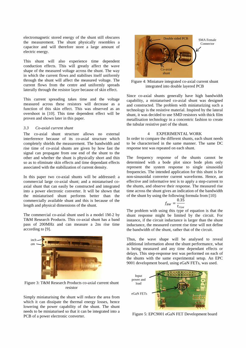
The co-axial shunt structure allows no external interference because of its co-axial structure which completely shields the measurement. The bandwidth and rise time of co-axial shunts are given by how fast the signal can propagate from one end of the shunt to the other and whether the shunt is physically short and thin so as to eliminate skin effects and time dependant effects associated with the stabilization of current density. In this paper two co-axial shunts will be addressed: a commercial large co-axial shunt; and a miniaturised co-axial shunt that can easily be constructed and integrated into a power electronic converter. It will be shown that the miniaturised shunt performs better than the commercially available shunt and this is because of the length and physical dimensions of the shunt. The commercial co-axial shunt used is a model 1M-2 by T&M Research Products. This co-axial shunt has a band pass of 200MHz and can measure a 2ns rise time according to [9].
Figure 3: T&M Research Products co-axial current shunt
resistor Simply miniaturising the shunt will reduce the area from which it can dissipate the thermal energy losses, hence lowering the power capability of the shunt. The shunt needs to be miniaturised so that it can be integrated into a PCB of a power electronic converter.
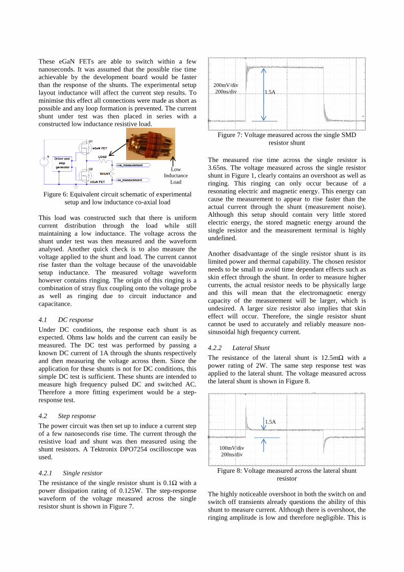
Figure 4: Miniature integrated co-axial current shunt
integrated into double layered PCB Since co-axial shunts generally have high bandwidth capability, a miniaturised co-axial shunt was designed and constructed. The problem with miniaturizing such a technology is the resistive material. Inspired by the lateral shunt, it was decided to use SMD resistors with thick film metallisation technology in a concentric fashion to create the tubular resistive part of the shunt.
4 EXPERIMENTAL WORK In order to compare the different shunts, each shunt needs to be characterised in the same manner. The same DC response test was repeated on each shunt. The frequency response of the shunts cannot be determined with a bode plot since bode plots only represent the system response to single sinusoidal frequencies. The intended application for this shunt is for non-sinusoidal converter current waveforms. Hence, an effective and informative test is to apply a step-current to the shunts, and observe their response. The measured rise time across the shunt gives an indication of the bandwidth of the shunt by using the following formula from [10]:
0.35
The problem with using this type of equation is that the shunt response might be limited by the circuit. For instance, if the circuit inductance is larger than the shunt inductance, the measured current rise time will not define the bandwidth of the shunt, rather that of the circuit. Thus, the wave shape will be analysed to reveal additional information about the shunt performance, what is being measured and any time dependant effects or delays. This step-response test was performed on each of the shunts with the same experimental setup. An EPC 9001 development board, using eGaN FETs, was used.
Figure 5: EPC9001 eGaN FET Development board
cm inch
SMA Female Connector
Co-axial shunt
Double sided PCB
eGaN FETs
Input power and
load terminals
These eGaN FETs are able to switch within a few nanoseconds. It was assumed that the possible rise time achievable by the development board would be faster than the response of the shunts. The experimental setup layout inductance will affect the current step results. To minimise this effect all connections were made as short as possible and any loop formation is prevented. The current shunt under test was then placed in series with a constructed low inductance resistive load.
Figure 6: Equivalent circuit schematic of experimental
setup and low inductance co-axial load This load was constructed such that there is uniform current distribution through the load while still maintaining a low inductance. The voltage across the shunt under test was then measured and the waveform analysed. Another quick check is to also measure the voltage applied to the shunt and load. The current cannot rise faster than the voltage because of the unavoidable setup inductance. The measured voltage waveform however contains ringing. The origin of this ringing is a combination of stray flux coupling onto the voltage probe as well as ringing due to circuit inductance and capacitance.
4.1 DC response
Under DC conditions, the response each shunt is as expected. Ohms law holds and the current can easily be measured. The DC test was performed by passing a known DC current of 1A through the shunts respectively and then measuring the voltage across them. Since the application for these shunts is not for DC conditions, this simple DC test is sufficient. These shunts are intended to measure high frequency pulsed DC and switched AC. Therefore a more fitting experiment would be a step-response test.
4.2 Step response
The power circuit was then set up to induce a current step of a few nanoseconds rise time. The current through the resistive load and shunt was then measured using the shunt resistors. A Tektronix DPO7254 oscilloscope was used.
4.2.1 Single resistor
The resistance of the single resistor shunt is 0.1Ω with a power dissipation rating of 0.125W. The step-response waveform of the voltage measured across the single resistor shunt is shown in Figure 7.
Figure 7: Voltage measured across the single SMD
resistor shunt The measured rise time across the single resistor is 3.65ns. The voltage measured across the single resistor shunt in Figure 1, clearly contains an overshoot as well as ringing. This ringing can only occur because of a resonating electric and magnetic energy. This energy can cause the measurement to appear to rise faster than the actual current through the shunt (measurement noise). Although this setup should contain very little stored electric energy, the stored magnetic energy around the single resistor and the measurement terminal is highly undefined. Another disadvantage of the single resistor shunt is its limited power and thermal capability. The chosen resistor needs to be small to avoid time dependant effects such as skin effect through the shunt. In order to measure higher currents, the actual resistor needs to be physically large and this will mean that the electromagnetic energy capacity of the measurement will be larger, which is undesired. A larger size resistor also implies that skin effect will occur. Therefore, the single resistor shunt cannot be used to accurately and reliably measure non-sinusoidal high frequency current.
4.2.2 Lateral Shunt
The resistance of the lateral shunt is 12.5mΩ with a power rating of 2W. The same step response test was applied to the lateral shunt. The voltage measured across the lateral shunt is shown in Figure 8.
Figure 8: Voltage measured across the lateral shunt
resistor The highly noticeable overshoot in both the switch on and switch off transients already questions the ability of this shunt to measure current. Although there is overshoot, the ringing amplitude is low and therefore negligible. This is
Low Inductance
Load
200mV/div 200ns/div
100mV/div 200ns/div
1.5A
1.5A
very important because it indicates that the overshoot is due to a time dependant effect. The way the current flows through the lateral shunt in accordance with the position from where the voltage is measured creates this overshoot. As current enters down the co-axial via it then spreads laterally. The current takes time to spread through the lateral resistor configuration. The potential across the resistor arrangement is initially high, since the current has not yet passed through the resistors, and as the current begins to flow through the resistors, the potential decreases until the current flows uniformly throughout the structure. The inverse happens for the switch off transient. This effect is seen as an overshoot in the measurement. This is enough reason to suggest that the lateral shunt is not suitable for high frequency switching current measurement. The rise time of the waveform is 126.3ps. This value is not reliable since the waveform that is being measured is not the true representation of the current. A better characterisation of this type of shunt can be done using the methods described in [10].
4.2.3 Co-axial shunt
Neither the single resistor nor the lateral shunts are suitable for high frequency switching current measurement. A common shunt which is used to measure large currents is a coaxial shunt. This type of shunt has a high bandwidth and is also electromagnetically defined. The effects of the time domain characteristics of the co-axial shunt are dependant only on its dimensions. Even then, the response time can be determined. The resistance of the T&M shunt is 10mΩ with a power rating of 20W. The same step- response measurement was taken using a conventional co-axial shunt from T&M Research Products. The step response measurement is shown in Figure 9.
Figure 9: Voltage measured across the T&M co-axial
shunt This shunt is physically much larger than the previous shunts discussed. Yet, unlike both the lateral as well as the single resistor shunt, the co-axial shunt does not show overshoot in the measurement. This is because the measurement is taken in the field free region. This means that the measurement is effectively shielded from any stray electromagnetic fields which can interfere with the measurement. Some ringing is observed in the
measurement. This ringing is due to the complex circuit layout impedance and the load impedance. The rise time was measured as 20ns. The datasheet for the 1M-2 co-axial model device states that this is a 2ns shunt [12]. So this must mean that the current is limited by the circuit and experimental setup. Miniaturising the co-axial shunt should yield better results. This is because the current distribution through a physically smaller co-axial shunt will reach a uniform value much quicker. To prove this, a miniaturised shunt is discussed next.
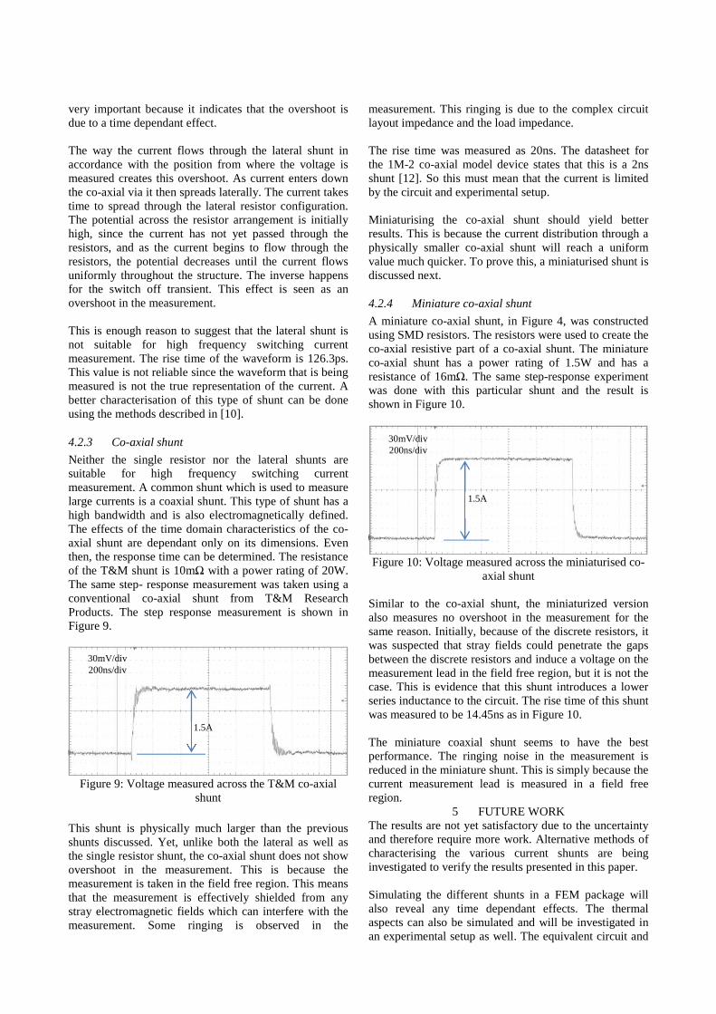
4.2.4 Miniature co-axial shunt
A miniature co-axial shunt, in Figure 4, was constructed using SMD resistors. The resistors were used to create the co-axial resistive part of a co-axial shunt. The miniature co-axial shunt has a power rating of 1.5W and has a resistance of 16mΩ. The same step-response experiment was done with this particular shunt and the result is shown in Figure 10.
Figure 10: Voltage measured across the miniaturised co-
axial shunt Similar to the co-axial shunt, the miniaturized version also measures no overshoot in the measurement for the same reason. Initially, because of the discrete resistors, it was suspected that stray fields could penetrate the gaps between the discrete resistors and induce a voltage on the measurement lead in the field free region, but it is not the case. This is evidence that this shunt introduces a lower series inductance to the circuit. The rise time of this shunt was measured to be 14.45ns as in Figure 10. The miniature coaxial shunt seems to have the best performance. The ringing noise in the measurement is reduced in the miniature shunt. This is simply because the current measurement lead is measured in a field free region.
5 FUTURE WORK The results are not yet satisfactory due to the uncertainty and therefore require more work. Alternative methods of characterising the various current shunts are being investigated to verify the results presented in this paper. Simulating the different shunts in a FEM package will also reveal any time dependant effects. The thermal aspects can also be simulated and will be investigated in an experimental setup as well. The equivalent circuit and
30mV/div 200ns/div
30mV/div 200ns/div
1.5A
1.5A
theoretical inherent parasitic elements of the various current shunts are also being considered. The equivalent-circuit impedance can also be used to verify the measured characteristics. Implementing the miniature integrated shunt into a HF and possibly RF switching power electronic converter circuit using GaN power transistors is also being looked into.
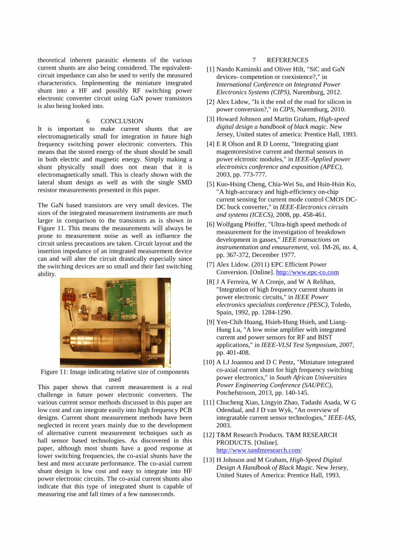
6 CONCLUSION It is important to make current shunts that are electromagnetically small for integration in future high frequency switching power electronic converters. This means that the stored energy of the shunt should be small in both electric and magnetic energy. Simply making a shunt physically small does not mean that it is electromagnetically small. This is clearly shown with the lateral shunt design as well as with the single SMD resistor measurements presented in this paper. The GaN based transistors are very small devices. The sizes of the integrated measurement instruments are much larger in comparison to the transistors as is shown in Figure 11. This means the measurements will always be prone to measurement noise as well as influence the circuit unless precautions are taken. Circuit layout and the insertion impedance of an integrated measurement device can and will alter the circuit drastically especially since the switching devices are so small and their fast switching ability.
Figure 11: Image indicating relative size of components
used This paper shows that current measurement is a real challenge in future power electronic converters. The various current sensor methods discussed in this paper are low cost and can integrate easily into high frequency PCB designs. Current shunt measurement methods have been neglected in recent years mainly due to the development of alternative current measurement techniques such as hall sensor based technologies. As discovered in this paper, although most shunts have a good response at lower switching frequencies, the co-axial shunts have the best and most accurate performance. The co-axial current shunt design is low cost and easy to integrate into HF power electronic circuits. The co-axial current shunts also indicate that this type of integrated shunt is capable of measuring rise and fall times of a few nanoseconds.
7 REFERENCES [1] Nando Kaminski and Oliver Hilt, "SiC and GaN
devices- competetion or coexistence?," in International Conference on Integrated Power Electronics Systems (CIPS), Nuremburg, 2012.
[2] Alex Lidow, "Is it the end of the road for silicon in power conversion?," in CIPS, Nuremburg, 2010.
[3] Howard Johnson and Martin Graham, High-speed digital design a handbook of black magic. New Jersey, United states of america: Prentice Hall, 1993.
[4] E R Olson and R D Lorenz, "Integrating giant magentoresistive current and thermal sensors in power elctronic modules," in IEEE-Applied power electroinics conference and exposition (APEC), 2003, pp. 773-777.
[5] Kuo-Hsing Cheng, Chia-Wei Su, and Hsin-Hsin Ko, "A high-accuracy and high-efficiency on-chip current sensing for current mode control CMOS DC-DC buck converter," in IEEE-Electronics circuits and systems (ICECS), 2008, pp. 458-461.
[6] Wolfgang Pfeiffer, "Ultra-high speed methods of measurement for the investigation of breakdown development in gasses," IEEE transactions on instrumentation and emasurement, vol. IM-26, no. 4, pp. 367-372, December 1977.
[7] Alex Lidow. (2011) EPC Efficient Power Conversion. [Online]. http://www.epc-co.com
[8] J A Ferreira, W A Cronje, and W A Relihan, "Integration of high frequency current shunts in power electronic circuits," in IEEE Power electronics specialists conference (PESC), Toledo, Spain, 1992, pp. 1284-1290.
[9] Yen-Chih Huang, Hsieh-Hung Hsieh, and Liang-Hung Lu, "A low noise amplifier with integrated current and power sensors for RF and BIST applications," in IEEE-VLSI Test Symposium, 2007, pp. 401-408.
[10] A LJ Joannou and D C Pentz, "Miniature integrated co-axial current shunt for high frequency switching power electronics," in South African Universities Power Engineering Conference (SAUPEC), Potchefstroom, 2013, pp. 140-145.
[11] Chucheng Xiao, Lingyin Zhao, Tadashi Asada, W G Odendaal, and J D van Wyk, "An overview of integratable current sensor technologies," IEEE-IAS, 2003.
[12] T&M Research Products. T&M RESEARCH PRODUCTS. [Online]. http://www.tandmresearch.com/
[13] H Johnson and M Graham, High-Speed Digital Design A Handbook of Black Magic. New Jersey, United States of America: Prentice Hall, 1993.