Embed Size (px)
Citation preview
P1: PJO
SVNY085-Sheng S. Li October 20, 2005 15:12
8Scattering Mechanisms and CarrierMobilities in Semiconductors
8.1. Introduction
The relaxation time approximation introduced in Chapter 7 enables one to lin-earize the Boltzmann transport equation in that the collision term is expressedin terms of the ratio of the perturbed distribution function (i.e., f − f0) and therelaxation time. This approximation allows one to obtain analytical expressionsfor different transport coefficients in semiconductors. However, detailed physicalinsights concerning the collision term and the validity of the relaxation time ap-proximation were not discussed in Chapter 7. In this chapter, various scatteringmechanisms associated with the collision term in the Boltzmann equation will bedepicted, and the relaxation time constants due to different scattering mechanismsin a semiconductor will be derived.
The collision term in the Boltzmann transport equation represents the inter-nal relaxation mechanisms, which are related to the collision of charged carriers(electrons or holes) with different scattering sources (e.g., scattering of electronsby acoustical phonons and ionized impurity) in a semiconductor under the in-fluence of external forces. These scattering mechanisms are responsible for thecharged carriers to reach steady-state conditions when the external forces are ap-plied to the semiconductor, and to return to the equilibrium conditions when theexternal forces are removed from the semiconductor. In the elastic scattering,the nonequilibrium distribution function will decay exponentially with time to itsequilibrium value after the external force is removed. The time constant associ-ated with this exponential decay is known as the relaxation time or the collisiontime.
In this chapter, several important scattering mechanisms such as acousticalphonon and optical phonon scatterings, ionized impurity scattering, and neutralimpurity scattering, which play a key role in determining the carrier mobilitiesin a semiconductor, will be considered. Using quantum mechanical treatmentsthe relaxation time expressions for these scattering mechanisms can be derived.In Section 8.2, the collision term is expressed in terms of the rate of transitionprobability and the distribution functions for the initial and final states in k-space.
211

P1: PJO
SVNY085-Sheng S. Li October 20, 2005 15:12
212 8. Scattering Mechanisms and Carrier Mobilities in Semiconductors
The differential scattering cross section, which is defined in terms of the rate oftransition probability and the incident flux of the scattering charged carriers, isalso introduced in this section. Using the Brooks–Herring (B-H) model, the relax-ation time for the ionized impurity scattering is derived in Section 8.3. Section 8.4describes the neutral impurity scattering, which is an important scattering sourceat very low temperatures or at very high doping densities. Using deformation po-tential theory, the scattering of charge carriers by the longitudinal-mode acousticalphonons is derived in Section 8.5. The scatterings of charge carriers by polar andnonpolar optical phonons in compound semiconductors as well as the intervalleyoptical phonon scattering in a multivalley semiconductor are depicted in Section8.6. The scattering of charge carriers by dislocations is described in Section 8.7.Finally, the measured Hall mobilities and drift mobilities for some elemental andcompound semiconductors are presented in Section 8.8.
In general, the charge carriers in a semiconductor may be scattered by sta-tionary defects (e.g., impurities and dislocations) and/or by dynamic defects (e.g.,electrons, holes, and lattice phonons). Therefore, the transport properties of a semi-conductor depend strongly upon the types of scattering mechanisms involved. Forexample, the electrical conductivity of an n-type semiconductor can be expressedin terms of the electron mobility and electron concentration by
σn = n0qµn, (8.1)
where n0 is the electron concentration, q is the electronic charge, and µn is theelectron mobility. The electron mobility may be defined in terms of the conductivityeffective mass m∗
c and the relaxation time τ by
µn = q〈τ 〉m∗
c
, (8.2)
where 〈τ 〉 is the average relaxation time defined by Eq. (7.54). Thus, the electronmobility is directly proportional to the average relaxation time and varies inverselywith the conductivity effective mass. Since the average relaxation time given inEq. (8.2) is directly related to the scattering mechanisms, in order to calculate thecarrier mobility, it is necessary to first consider the scattering mechanisms in asemiconductor.
In the relaxation time approximation, the collision term in the Boltzmann equa-tion can be expressed in terms of the perturbed distribution function divided bythe relaxation time. From Eq. (7.25), one obtains
∂ f
∂t
∣∣∣∣c
= − f − f0
τ, (8.3)
where f is the nonequilibrium distribution function and f0 is the equilibrium Fermi–Dirac distribution function. As mentioned earlier, the relaxation time approxima-tion is valid only for the elastic-scattering case. This condition is satisfied so longas the change in energy of the charge carriers before and after each scattering eventis small compared to the initial carrier energy. In fact, a generalized expressionfor the collision term given by Eq. (8.3) can be formulated in terms of the rate

P1: PJO
SVNY085-Sheng S. Li October 20, 2005 15:12
8.1. Introduction 213
of transition probability Pkk ′ and the nonequilibrium distribution function f (k, r ),which is given by
− ∂ fk ′
∂t
∣∣∣∣c
=∑
k ′[Pkk ′ fk ′ (1 − fk) − Pkk ′ fk (1 − fk ′ )], (8.4)
where Pkk ′ is the rate of transition probability from the final state k ′ to the initialstate k, and Pkk ′ is the rate of transition probability from the k-state to the k ′-state. The electron distribution function in the k ′-state is designated by fk ′ , and theelectron distribution function in the k-state is represented by fk .
The right-hand side of Eq. (8.4) represents the net transition rates from the k-to k ′-state summed over all the final states, k ′. The summation in Eq. (8.4) can bereplaced by integration over the entire conduction band if all the quantum statesin the band are treated as quasi-continuum. Since the density of quantum states inthe conduction band is very large and the spacing between each quantum state isso small, such an assumption is usually valid. Therefore, it is a common practiceto replace the summation in Eq. (8.4) by an integral, which can be written as
− ∂ fk ′
∂t
∣∣∣∣c
= N�
(2π )3
∫[Pk ′k fk ′ (1 − fk) − Pkk ′ fk (1 − fk ′ )] d3k ′
= N�
(2π )3
∫Pkk ′ ( fk ′ − fk) d3k ′, (8.5)
where Pkk ′ is assumed equal to Pk ′k ′ , N is the total number of unit cells in thecrystal, and � is the volume of the unit cell.
It is noted that the collision term given by Eq. (8.5) is a differential integralequation and cannot be solved analytically without further approximations. In or-der to derive an analytical expression for Eq. (8.5), it is useful to first consider thesmall-perturbation case (i.e., the low-field case). In this case, the nonequilibriumdistribution function f (k, r ) can be expressed in terms of the equilibrium distri-bution function f 0
k and a first-order perturbing distribution function f 1k , which
reads
fk = f 0k + f 1
k + · · ·fk ′ = f 0
k ′ + f 1k ′ + · · · , (8.6)
where f 0k and f 0
k ′ are the Fermi–Dirac distribution functions in the k- and k ′-states,while f 1
k and f 1k ′ denote the first-order correction terms of the distribution functions
in the k-and k ′-state, respectively.If one assumes that the scattering is elastic, then the energy change during
scattering processes is small compared to the average electron energy. Under thiscondition, the average energy of electrons in the initial and final states can beassumed equal (i.e., Ek = Ek ′ ). Therefore, the equilibrium distribution functionsfor the initial and final states are identical, and the collision term can be simplifiedto
− ∂ fk ′
∂t
∣∣∣∣c
= f 1k ′
τ= N�
(2π )3
∫Pkk ′
(f 1k ′ − f 1
k
)d3k ′. (8.7)

P1: PJO
SVNY085-Sheng S. Li October 20, 2005 15:12
214 8. Scattering Mechanisms and Carrier Mobilities in Semiconductors
Thus, the inverse relaxation time τ−1 can be written as
1
τ= N�
(2π )3
∫Pkk ′
(1 − f 1
k
f 1k ′
)d3k ′. (8.8)
Furthermore, if one assumes that the scattering process is isotropic, then the ratioof f 1
k and f 1k ′ can be expressed in terms of cos θ ′, where θ ′ is the angle between
the k- and k ′-states (see Figure 8.2b). Under this condition, Eq. (8.8) becomes
1
τ= N�
(2π )3
∫Pkk ′
(1 − cos θ ′) d3k ′. (8.9)
Equation (8.9) shows that the scattering rate, τ−1 of the charge carriers for isotropicelastic scattering depends only on the angle θ ′ between the k- and k ′-state and therate of transition probability Pkk ′ .
In order to derive the relaxation time for a specific scattering process, both therate of transition probability and the differential scattering cross section must bedetermined first. This is discussed next.
8.2. Differential Scattering Cross-Section
In the present treatment, it is assumed that the scattering of charge carriers isconfined within a single energy band (e.g., electrons in the conduction band andholes in the valence band), as illustrated in Figure 8.1a. Other important scatteringprocesses such as intervalley scattering for the multivalley semiconductors suchas Si and Ge and interband scattering in the heavy-hole and light-hole bands arealso shown in Figure 8.1b and c, respectively.
Figure 8.1. Scattering of electrons in the k-space of a semiconductor: (a) The intravalleyscattering of electrons in the conduction band and the intraband scattering of holes in thevalence band, (b) intervalley scattering of electrons in the conduction band, and (c) interbandscatterng of holes in the valence bands; k is the wave vectors of incident electron and k′ isthe wave vector of scattered electron in k-space.
P1: PJO
SVNY085-Sheng S. Li October 20, 2005 15:12
8.2. Differential Scattering Cross-Section 215
The intraband and intravalley scatterings shown in Figure 8.1a are usuallyaccompanied by the absorption or emission of a longitudinal-mode acousticalphonon, and hence can be considered as elastic scattering. However, the interbandand intervalley scatterings shown in Figure 8.1b and c are usually inelastic becausethe change in electron energy for these scatterings is no longer small comparedto the average electron energy. The intervalley and interband scattering processesare usually accompanied by the absorption or emission of optical phonons, whichoccur at high temperatures or high electric fields.
The rate of transition probability Pkk ′ in a scattering event can be derivedfrom the one-electron Schrodinger equation. The one-electron time-independentSchrodinger equation for the initial unperturbed states is given by
H0φk (r ) = Ekφk(r ), (8.10)
where
H0 = −h--2∇2
2m∗ + V (r ). (8.11)
H0 is the unperturbed Hamiltonian, and φk(r ) is the initial unperturbed electronwave function given by
φk(r ) = uk(r ) eik,r , (8.12)
where uk(r ) is the Bloch function, which has the same periodicity as the crystalpotential V (r ).
When a small perturbation (e.g., a small electric field) is applied to the crystal,the electron may be scattered from the initial state, k into the final state, k ′. Theperturbed Hamiltonian under this condition can be written as
H = H0 + H ′, (8.13)
where H0 is the unperturbed Hamiltonian given by Eq. (8.11), and H ′ is the first-order correction due to perturbation. The time-dependent Schrodinger equationunder the perturbed condition is given by
Hψk(r, t) = −ih--∂ψk(r, t)
∂t, (8.14)
which has a solution given by
ψk(r, t) =∑
k
ak(t) e−i Ek t/h-- φk(r ), (8.15)
where ak(t) is the time-dependent amplitude function, and φk(r ) is the unperturbedelectron wave function defined by Eq. (8.12).
According to time-dependent perturbation theory, the transition probability perunit time from k- to k ′-state can be expressed in terms of the amplitude functionak(t) by
Pk ′k(t) = |ak(t)|2t
. (8.16)
P1: PJO
SVNY085-Sheng S. Li October 20, 2005 15:12
216 8. Scattering Mechanisms and Carrier Mobilities in Semiconductors
Similarly, the transition probability per unit time from k ′- to k-state is given by
Pkk ′ (t) = |ak ′ (t)|2t
. (8.17)
From the principle of detailed balance, one can assume that Pkk ′ = Pk ′k . UsingEqs. (8.14) through (8.17) and the orthogonal properties of electron wave functions,it can be shown from quantum mechanical calculations that the rate of transitionprobability Pkk ′ in the presence of a step perturbation function (i.e., a constant H ′)is given by
Pkk ′ =∣∣a′
k(t)∣∣2
t= 2π
h--|Hkk ′ |2 δ(Ek ′ − Ek), (8.18)
where
Hkk ′ = ⟨k ′ ∣∣H ′∣∣ k
⟩ = 1
(N�)
∫N�
φ∗k ′ H ′φk d3r (8.19)
is the matrix element. In Eq. (8.19), H ′ is the perturbing Hamiltonian, φk is theelectron wave function given by Eq. (8.12), and φ∗
k ′ is the complex conjugate ofφk ′ . The function δ(Ek ′ − Ek) is the Dirac delta function, which is equal to unityfor Ek = Ek ′ and vanishes otherwise.
The matrix element Hkk ′ , given by Eq. (8.19), has a finite value only if thegolden selection (momentum conservation) rule is satisfied (i.e., k = k ′ for a directtransition and k ′ = k ± q for an indirect transition). Calculations of relaxation timecan be simplified by introducing a differential scattering cross section σ (θ ′, φ′)in the relaxation time formula. It is noted that σ (θ ′, φ′) depends only on θ ′ if thescattering process is isotropic (i.e., independent of φ′). Under this condition, asimple relationship exists between σ (θ ′) and the rate of transition probability Pkk ′ .In general, the differential scattering cross section σ (θ ′, φ′) is defined as the totalnumber of particles which make transitions from k- to k ′ -states per unit solid angleper unit time divided by the incident flux density. This can be written as
σ (θ ′, φ′) =N�
(2π )3Pkk ′
d3k ′
dωvk
N�
= (N�)2 Pkk ′d3k ′
(2π )3vk sin θ ′dθ ′dφ′ , (8.20)
where vk is the initial particle velocity, N� is the volume of the crystal, anddω = sin θ ′ dθ ′ dφ′ is the solid angle between the incident wave vector k and thescattering wave vector k ′ (see Figure 8.2).
Now consider the case of an isotropic elastic scattering. Substituting Eqs. (8.18)and (8.19) into Eq. (8.20), and using the relationships vk = vk ′ , k = k ′, and d3k ′ =k2 sin θ ′ dθ ′ dφ′ dk ′, one can obtain an expression for the differential scatteringcross section, which is given by
σ (θ ′) = (N�)2k ′2 |Hkk ′ |2(2πh--vk ′ )2
. (8.21)

P1: PJO
SVNY085-Sheng S. Li October 20, 2005 15:12
8.3. Ionized Impurity Scattering 217
Figure 8.2. Scattering of electrons by a positively charged shallow-donor impurity atomin k-space.
The relaxation time τ is related to the total scattering cross section by
1
τ= NTσTvth, (8.22)
where NT is the density of total scattering centers, σT is the total scattering crosssection, and vth is the mean thermal velocity [vth = (3kBT/m∗)1/2]. The totalscattering cross section (σT) for the isotropic elastic scattering process can becalculated from Eq. (8.23) using the differential scattering cross section given byEq. (8.21), which can be expressed by
σT = 2π
∫ π
0σ (θ ′)(1 − cos θ ′) sin θ ′ dθ ′. (8.23)
Substituting Eq. (8.21) into Eq. (8.23), the total scattering cross section can beobtained from Eq. (8.23) provided that the perturbing Hamiltonian H ′, and hencethe matrix element Hkk ′ , is known. In the following sections, Eqs. (8.20) through(8.23) will be used to derive the expressions of relaxation time constants and carriermobilities for a semiconductor in which scatterings of electrons or holes are dueto the ionized impurities, neutral impurities, or the longitudinal mode acousticalphonons.
8.3. Ionized Impurity Scattering
Scattering of electrons by the ionized shallow-donor impurities is a classical ex-ample of elastic scattering in a semiconductor. This is due to the fact that the massof a shallow-donor impurity atom is much larger than that of an electron. As aresult, the change of electron energy during such a scattering event is negligiblecompared to the electron energy before the scattering. Therefore, the relaxationtime approximation given by Eq. (8.22) is valid in this case. In order to derive thedifferential scattering cross section and the relaxation time for the ionized impurityscattering, the matrix element Hkk ′ and the perturbing Hamiltonian H ′ due to the
P1: PJO
SVNY085-Sheng S. Li October 20, 2005 15:12
218 8. Scattering Mechanisms and Carrier Mobilities in Semiconductors
Figure 8.3. Potential due to a positively charged shallow-donor impurity atom: (a) bareCoulomb potential, (b) screening Coulomb potential, and (c) trajectory of electron scatteringby a positively charged ion.
shallow-donor impurity potential must be determined first. Let us consider thescattering of electrons by a positively charged shallow-donor impurity in an n-type semiconductor, as shown in Figure 8.2a. If the donor impurity is ionized witha single net positive charge, then the potential due to this ionized donor atom, ata large distance from the impurity atom, can be approximated by a bare Coulombpotential
V (r ) = q
4πε0εsr. (8.24)
It should be noted that Eq. (8.24) did not consider the Coulomb screening effect dueto electrons from the rest of positively charged donor ions in the semiconductor. Totake into account the screening effect of these electrons, it is necessary to replacethe bare Coulomb potential by a screening Coulomb potential in the derivationof ionized impurity scattering mobility. As shown in Figure 8.3b, if the screeningeffect of the shallow-donor ion by the surrounding conduction electrons is included,then the screening Coulomb potential (also known as the Yukawa potential) forthe ionized impurity atom can be expressed by
V ′(r ) = qe−r/λD
4πε0εsr, (8.25)
where
λD =√
ε0εskBT
q2n0(8.26)
is the Debye screen length.In deriving the matrix element for the ionized impurity scattering, Conwell and
Weisskopf(1) used the bare Coulomb potential given by Eq. (8.25) as the perturb-ing Hamiltonian, while Brooks and Herring(2) employed the screening Coulomb(Yukawa) potential given by Eq. (8.25) as the perturbing Hamiltonian. It will beshown later that the relaxation-time formula derived from both models differs onlyby a constant but gives the same prediction concerning the energy dependence of
P1: PJO
SVNY085-Sheng S. Li October 20, 2005 15:12
8.3. Ionized Impurity Scattering 219
the relaxation time. Since the Brooks–Herring (B-H) model is based on the quan-tum mechanical principle, and is fundamentally much more sound and accuratethan the Conwell–Weisskopf (C-W) model, it is pertinent here to use the B-Hmodel for the derivation of ionized impurity scattering mobility in a semiconduc-tor. The perturbing Hamiltonian due to the Yukawa potential, given by Eq. (8.25),can be written as
H ′ = qV ′(r ) = q2e−r/λD
4πε0εsr. (8.27)
Based on the Bloch theorem, the electron wave functions for the k-state can beexpressed by
φk(r ) =(
1
N�
)1/2
uk(r ) eik·r . (8.28)
The matrix element due to Yukawa potential can be derived using Eqs. (8.19),(8.27), and (8.28), and the result yields
Hkk ′ = 1
N�
∫e−ik ′ ·r
(q2e−r/λD
4πε0εsr
)eik·r d3r
= q2
2N�ε0εs
∫ π
0
∫ ∞
0e−ik·r
(e−r/λD
r
)r2 sin θr dθr dr (8.29)
= q2λ2D
N�ε0εs(1 + K 2λ2
D
) ,
where d3r = 2πr2 sin θr dθr dr is the volume element, and
K = k ′ − k = 2 |k| sin
(θ ′
2
). (8.30)
K is the reciprocal lattice vector. Figure 8.4 shows the relationship between theincident and scattered wave vectors k and k ′ in the real space.
Figure 8.4. Coordinates for computing the matrixelement of scattering by an ionized impurity, wherek is the wave vector of the incident electron, k ′
is the wave vector of the scattered electron wave,and K = k ′ – k = 2|k| sin (θ ′/2), is the reciprocallattice vector.
P1: PJO
SVNY085-Sheng S. Li October 20, 2005 15:12
220 8. Scattering Mechanisms and Carrier Mobilities in Semiconductors
The differential scattering cross section can be obtained by substitutingEq. (8.29) into Eq. (8.21), which yields
σ(θ ′) =
(q2m∗λ2
D
)2(2πh--2ε0εs
)2 (1 + K 2λ2
D
)2 = 4λ4D
a2B
(1 + K 2λ2
D
)2 , (8.31)
where
aB = 4πε0εsh--2
m∗q2(8.32)
is the Bohr radius for the ground state of the impurity atom.The relaxation time for the ionized impurity scattering can be obtained by sub-
stituting Eq. (8.31) into Eqs. (8.22) and (8.23), and the result is given by
1
τI= (2π NI v)
∫ π
0
4λ4D(1 − cos θ ′) sin θ ′ dθ ′
a2B
[1 + 4λ2
Dk2 sin2(θ ′/2)]2
= (2π NIv)
(λ4
D
a2B
) (1
kλD
)4
L(2kλD)
(8.33)
where
L(2kλD) = ln(1 + 4k2λ2
D
) − 4k2λ2D(
1 + 4k2λ2D
) ∼= ln(4k2λ2
D
), for kλD � 1 (8.34)
It is noted that L(2kλD) is a slow varying function of temperature and electron den-sity, and 4k2λ2
D = 8m∗Eε0εskBT/h--2q2n′, and n′ = n + (ND − N−A − n)(N−
A +n)/ND is the density of screening electrons surrounding the ionized donor im-purity. The integration of Eq. (8.33) can be carried out by letting sin(θ ′/2) =x, (1 − cos θ ′) = 2x2, sin θ ′dθ ′ = 4x dx , and using the table of integrals.
Equation (8.33) is the result of using the Brooks–Herring’s (B-H) model, andhence is known as the Brooks–Herring formula for the ionized impurity scattering.By using the relation E = h--2k2/2m∗, and substituting Eqs. (8.26) and (8.32) intoEq. (8.33), one obtains the inverse relaxation time as
1
τI= q4 NIL(2kλD)
16π (2m∗)1/2ε20ε
2s E3/2
. (8.35)
Equation (8.35) shows that for ionized impurity scattering, the relaxation time τI
is directly proportional to the energy to the power of three halves (i.e., τI ∝ E3/2).The temperature dependence of τI comes only from the variation of L(2kλD) withT, which is usually very small.
By substituting τI, given by Eq. (8.35), into Eq. (8.2), and by averaging τI overthe energy with the aid of Eq. (7.45), one obtains the ionized impurity scatteringmobility µI, which reads
µI = q 〈τI 〉m∗ = 64
√πε2
0ε2s (2kBT )3/2
NI q3√
m∗ ln
(12m∗k2
BT 2ε0εs
q2h--2n′
) , (8.36)

P1: PJO
SVNY085-Sheng S. Li October 20, 2005 15:12
8.4. Neutral Impurity Scattering 221
which shows that the ionized impurity scattering mobility µI is directly propor-tional to the temperature to the power of three halves (i.e., µI ∝ T 3/2). Goodagreement has been found between the theoretical prediction given by Eq. (8.36)and mobility data for different semiconductors in which the ionized impurity scat-tering is the dominant scattering mechanism.
Conwell and Weisskopf used the bare Coulomb potential as the perturbingHamiltonian and derived the relaxation-time formula for the ionized impurityscattering given by
1
τ ′I
= q4 NI
16π (2m∗)1/2ε20ε
2s E3/2
ln[1 + (2E/Em)2], (8.37)
where Em = q2/4πε0εsrm and NI = (2rm)−3. The ionized impurity scattering mo-bility derived from Eq. (8.37) is given by
µ′I = 64
√πε2
0ε2s (2kBT )3/2
NIq3m∗1/2 ln
[1 +
(12πε0εskBT/q2 N 1/3
I
)2] . (8.38)
Equation (8.38) is known as the Conwell–Weisskopf formula for the ionizedimpurity scattering. Comparing Eqs. (8.36) and (8.38) reveals that both formulasare very similar except that the coefficient inside the logarithmic term is slightlydifferent. It is of interesting to note that both formulas predict the same tempera-ture dependence for the ionized impurity scattering mobility and the same energydependence for the relaxation time.
8.4. Neutral Impurity Scattering
Neutral impurity scattering is an important source of resistance in a semiconductorat very low temperatures. As the temperature decreases, carrier freeze-out occursat the shallow-level impurity centers in an extrinsic semiconductor, and theseshallow-level impurities become neutral at very low temperatures. The scatteringpotential due to a neutral shallow-level impurity center may be described by asquare-well potential, which becomes the dominant scattering source for electronsor holes at very low temperatures.
In general, the scattering of charge carriers by the neutral shallow-donor orshallow-acceptor impurities can be treated in a similar way as that of scattering ofelectrons by a hydrogen atom. The neutral shallow-donor atom in a semiconductorcan be treated as a hydrogenic neutral atom immersed in the dielectric medium ofthe semiconductor whose dielectric constant is equal to the host semiconductor.
Erginsoy (3) derived the neutral impurity scattering mobility for a semiconductorusing the partial wave technique to obtain the differential scattering cross section.In the derivation, Erginsoy assumed that the electron velocity is low, and elasticscattering prevails in the semiconductor. Based on his derivation, the total differ-ential scattering cross section for the neutral impurity scattering can be written
P1: PJO
SVNY085-Sheng S. Li October 20, 2005 15:12
222 8. Scattering Mechanisms and Carrier Mobilities in Semiconductors
as
σN ≈ 20aB
k, (8.39)
where aB is the Bohr’s radius given by Eq. (8.32). Using Eqs. (8.22) and (8.39),the relaxation time for the neutral impurity scattering can be expressed by
τN = (NNvthσN)−1 = k
20aB NNv. (8.40)
Substituting aB given by Eq. (8.32) and k = m∗v/h-- into Eq. (8.40), one obtains
1
τN= 10ε0εs NNh3
π2m∗2q2, (8.41)
where NN is the density of neutral impurities. Since the relaxation time for neutralimpurity scattering is independent of energy, the mobility due to neutral impurityscattering can be readily obtained from Eq. (8.41), which yields
µN = qτN
m∗ = π2m∗q3
10ε0εs NNh3, (8.42)
which shows that the carrier mobility due to neutral impurity scattering is in-dependent of temperature. However, experimental results show that the carriermobility is generally a weak function of temperature for many semiconductors atlow temperatures.
8.5. Acoustical Phonon Scattering
Scattering of electrons by longitudinal-mode acoustical phonons is depicted in thissection. The scattering of electrons by the longitudinal-mode acoustical phonons isthe most important scattering source in intrinsic or lightly doped semiconductors.The scattering of electrons by the longitudinal-mode acoustical phonons can usu-ally be treated as an elastic scattering because the electron energy is much largerthan the phonon energy and the change in electron energy during such scatteringprocess is small compared to the average energy of electrons. It can be shown thatthe maximum change of electron energy due to the acoustical phonon scatteringis given by
E ≈ 4
(us
vth
)Ee, (8.43)
where us = 3 × 105 cm/s is the velocity of sound in a solid, and vth is the meanthermal velocity of electrons (∼107 cm/s). Thus, the ratio of phonon energy tomean electron energy as given by Eq. (8.43) is usually much smaller than unity forT > 100 K. At very low temperatures, mean electron energy may become com-parable to the acoustical phonon energy, and the assumption of elastic scatteringmay no longer be valid. Fortunately, at very low temperatures other types of scat-tering such as the ionized impurity and neutral impurity scattering may become

P1: PJO
SVNY085-Sheng S. Li October 20, 2005 15:12
8.5. Acoustical Phonon Scattering 223
dominant. It is noted that acoustical phonons may cause scattering in two differentways, either through deformation potential scattering or piezoelectric scattering.An acoustical wave may induce a change in the spacing of neighboring atomsin a semiconductor. This change in atomic spacing could result in the fluctuationof energy band gap locally on an atomic scale and is known as the deformationpotential. The deformation potential is measured as the change of energy bandgap per unit strain due to the acoustical phonons. This type of scattering is usuallythe most important scattering source for the intrinsic or lightly doped silicon andgermanium at room temperatures.
The piezoelectric scattering is another type of acoustical phonon scattering. Thistype of scattering is observed in III-V and II-VI compound semiconductors withthe zincblende and wurtzite crystal structures. The lack of inversion symmetry inthese semiconductors creates a strain-induced microscopic electric field pertur-bation, which leads to the piezoelectric scattering with emission or absorption ofan acoustical phonon. This type of scattering is important for pure III-V and II-VI compound semiconductors at low temperatures. These two types of acousticalphonon scattering are discussed next.
8.5.1. Deformation Potential Scattering
To derive the expression of relaxation time for the nonpolar acoustical phononscattering, the deformation potential technique developed originally by Bardeenand Shockley(4) for calculating the matrix element of longitudinal-mode acousti-cal phonon scattering will be discussed first. The perturbing Hamiltonian can beobtained from the deformation potential shown in Figure 8.5. Figure 8.5a showsthe change of lattice spacing with respect to its equilibrium position due to lat-tice vibration. It is seen that thermal expansion and contraction of the lattice withtemperature can lead to a change of the conduction and valence band edges or theenergy band gap of the semiconductor, as is shown in Figure 8.5b. Based on the de-formation potential model proposed by Shockley, the fluctuation of the conduction
Figure 8.5. The change of conduction band edge and the deformation potential due tothermal expansion or contraction of the lattice spacing.
P1: PJO
SVNY085-Sheng S. Li October 20, 2005 15:12
224 8. Scattering Mechanisms and Carrier Mobilities in Semiconductors
band edge due to the lattice vibrations may be represented by a deformation po-tential. Therefore, the perturbing Hamiltonian can be related to the change ofcrystal volume caused by the lattice phonons and the deformation potential by theexpression
H ′ = Ec − Eco =(
Ec
V
) V = Ec1
( V
V
), (8.44)
where Eco is the conduction band edge in thermal equilibrium, and
Ec1 = Ec/ T
V/V T(8.45)
is the deformation potential constant. For silicon, Ec1 = −16 eV, and for germa-nium, Ec1 = −9.5 eV. The ratio V/V represents the change of crystal volumeto the total crystal volume due to temperature change in a semiconductor. Since V/V can be expanded in terms of a Fourier series in the atomic displacement rn ,one can write
V
V= ∇r · rn, (8.46)
where
rn =3∑
j=1
(1/N )1/2ζ j b j (q) eiq·Rn0 e−iωt . (8.47)
The lattice displacement rn given by Eq. (8.47) can be expressed in terms of thenormal coordinates and normal frequencies in three-dimensional form (i.e., twotransverse branches and one longitudinal branch). It is also assumed that only thelongitudinal-mode acoustical phonon scattering is important in the present case.Therefore, under this condition ∇r · rn can be expressed by
∇r · rn =∑
q
qlrl, (8.48)
where ql is the wave vector of the longitudinal-mode acoustical phonon, and rl
represents the displacement due to longitudinal-mode acoustical phonons. Sub-stituting Eqs. (8.46) and (8.48) for (∇V/V ) into Eq. (8.44) yields the perturbingHamiltonian H ′, which is given by
H ′ = Ec1
( V
V
)= Ec1
∑q
qlrl. (8.49)
The matrix element Hkk ′qq ′ due to this perturbing Hamiltonian can be expressedas
Hkk ′qq ′ = ⟨k ′nq ′
∣∣H ′∣∣ knq⟩
=∫
φ∗k ′ϕ
∗nq
(∑q
Ec1qlrl
)φkϕnq d3r d3rl, (8.50)
P1: PJO
SVNY085-Sheng S. Li October 20, 2005 15:12
8.5. Acoustical Phonon Scattering 225
where ϕnq is the phonon wave functions and φk is the electron wave functions. Forphonon emission, the solution of Eq. (8.50) for the matrix element is given by
Hkk ′qq ′ =(
Ec1ql
N�
)(h--
Mω
)1/2(⟨
nq⟩
2
)1/2
(8.51)
and for phonon absorption it is given by
Hkk ′qq ′ =(
Ec1ql
N�
) (h--
Mω
)1/2[(⟨
nq⟩ + 1
)2
]1/2
. (8.52)
In Eqs. (8.51) and (8.52), N� is the volume of the crystal, M is the mass of theatom, and
⟨nq
⟩is the average phonon population density given by
⟨nq
⟩ = 1
(eh--ω/kBT − 1)≈ kBT
h--ω. (8.53)
Equation (8.53) is valid for long-wavelength acoustical phonons (i.e., kBT � h--ωand eh-- ω/kT
B ≈ 1 + h--ω/kBT ). The square of the matrix element due to the deforma-tion potential scattering can be obtained from the summation of the square of Eqs.(8.51) and (8.52) and using the dispersionless relation ω = usql, which yields
∣∣Hkk ′qq ′∣∣2 = E2
clkBT
M(us N�)2. (8.54)
Now, substituting∣∣Hkk ′qq ′
∣∣2given by Eq. (8.54) into Eq. (8.21) yields the dif-
ferential scattering cross section, which reads
σa = m∗2 E2c1kBT
4π2h--4ρu2s
= m∗2 E2c1kBT
4π2h--4cl, (8.55)
where ρ = M/� is the mass density of the atom, and � is the volume of theunit cell; cl = ρu2
s is the longitudinal elastic constant. For a cubic crystal, cl = c11
for wave propagating along the (100) direction; for a (110) direction cl = (c11 +c12 + c44)/2, and for a (111) propagation direction cl = (c11 + 2c12 + 4c44)/3,where c11, c12, and c44 are components of the elasticity tensor.
The relaxation time due to the longitudinal-mode acoustical phonon scatteringcan be obtained by substituting Eq. (8.55) into Eqs. (8.23) and (8.22), and theresult yields
1
τa= 2πν
∫ π
0σa sin θ ′(1 − cos θ ′) dθ ′
= m∗2vE2c1kBT
πh--4cl= v
la,
(8.56)
where la = πh--4cl/m∗2E2c1kBT is the mean free path of electrons, which varies
inversely with temperature. Substituting v = (2E/m∗)1/2 into Eq. (8.56) yields

P1: PJO
SVNY085-Sheng S. Li October 20, 2005 15:12
226 8. Scattering Mechanisms and Carrier Mobilities in Semiconductors
1/τa as
1
τa= m∗3/2
n kBT E2c1(2E)1/2
πh--4cl, (8.57)
which shows that for acoustical phonon scattering τa varies with E−1/2 and T −1.The electron mobility due to acoustical phonon scattering can be obtained bysubstituting τa given by Eq. (8.57) into Eq. (7.64), and the result yields
µa = q 〈τa〉m∗
c
=(
2√
2πqh--4cl
3m∗3/2n m∗
ck3/2B E2
c1
)T −3/2, (8.58)
where m∗c is the conductivity effective mass of electrons. For cubic crystals with
ellipsoidal constant-energy surfaces, the effective mass product mcm∗3/2n is given
by
1
mcm∗3/2n
= 1
3m tm1/2l
(2
m t+ 1
m l
), (8.59)
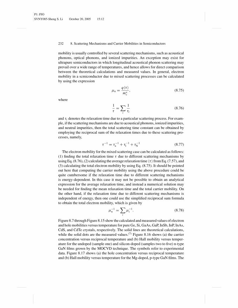
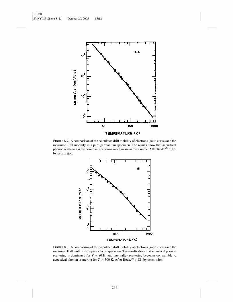
where m t and m l are the transverse and longitudinal effective masses of electrons inthe ellipsoidal conduction band valley, respectively. Equation (8.58) predicts thatthe electron mobility due to longitudinal-mode acoustical phonon scattering isdirectly proportional to T −3/2. Figures 8.7 and 8.8 show the experimental resultsfor electron mobilities in the undoped germanium and silicon crystals, whichwere found to be in good agreement with theoretical predictions for T < 200 K.However, at high temperatures, intervalley optical phonon scattering contributessubstantially to electron mobility, and hence µn varies as T −n , where n lies between1.5 and 2.7.
8.5.2. Piezoelectric Scattering
For polar semiconductors such as III-V and II-VI compound semiconductors, thebonds are partially ionic, and the unit cell does not possess inversion symmetry.As a result, charged carriers may be scattered by longitudinal-mode acousticalphonons due to piezoelectric scattering. In general, the strain-induced electricfield due to the piezoelectric effect can be represented by
Epz = −(
epz
ε0εs
)(∇r rn) , (8.60)
where epz is the piezoelectric constant. Thus, the perturbation potential due topiezoelectric scattering can be expressed by
H ′ = eEpz
q=
(|e| epz
ε0εsq
)(∇r rn) , (8.61)
where q = |k ′ − k| = 2k sin(θ ′/2) = (2m∗v/h--) sin(θ ′/2) is the phonon wave vec-tor, and |e| is the electronic charge. A comparison of Eq. (8.61) with Eq. (8.49) forthe nonpolar acoustical phonon scattering reveals that, instead of the deformation
P1: PJO
SVNY085-Sheng S. Li October 20, 2005 15:12
8.5. Acoustical Phonon Scattering 227
potential constant Ec1, one has |e|epz/ε0εsq, which is not a constant (since q de-pends on v and θ ′). Thus, the matrix element Hkk ′ due to piezoelectric scatteringcan be written as
Hkk ′ = |e| epz
ε0εsq
(kBT
2V cl
)1/2
=(
e2 K 2kBT
2V ε0εsq2
)1/2
(8.62)
In Eq. (8.62) a dimensionless electromechanical coupling constant, K 2, is intro-duced, which is defined by
K 2
1 − K 2= e2
pz
ε0εscl. (8.63)
The left-hand side of Eq. (8.63) reduces to K 2 if K 2 � 1. For most polar semi-conductors, value of K 2 is in the order of 10−3.
The relaxation time due to piezoelectric scattering can be obtained by substitut-ing Eq. (8.62) into Eqs. (8.18) and (8.9), which yields
1
τpz= V
(2π )2
∫2
(2π
h--
) (e2 K 2kBT
2V ε0εsq2
)δ(Ek − Ek ′ )k ′2 (1 − cos θ ′) sin θ ′dθ ′ dk ′,
(8.64)
where q2 = 4k ′2 sin2(θ ′/2) and dk ′ = h--−1(m∗/2E)1/2 dE . Now carrying out theintegration in Eq. (8.64) one obtains
τpz = 23/2πh--2ε0εs
m∗1/2e2 K 2kBTE1/2, (8.65)
which shows that the relaxation time for piezoelectric scattering is proportionalto the square root of the energy. Thus, the carrier mobility due to piezoelectricscattering can be derived using the expression of τpz given by Eq. (8.65) and (8.2),and the result yields
µpz = 16√
2πh--2ε0εs
3m∗3/2|e|K 2(kBT )1/2. (8.66)
Equation (8.66) shows that the piezoelectric scattering mobility depends on T −1/2.For a typical III-V compound semiconductor with εs = 12, m∗/m0 = 0.1, andK 2 = 10−3, a mobility value of 1.7 × 105 cm2/(V s) was obtained for piezoelec-tric scattering at T = 300 K. This value is significantly higher than the deformationpotential scattering mobility for most polar semiconductors. Therefore, piezoelec-tric scattering is usually not as important as acoustical phonon scattering due todeformation potential or ionized impurity scattering. Thus, the piezoelectric scat-tering has little influence on electron mobilities for most III-V compound semicon-ductors. However, piezoelectric scattering can become important for many II-VIcompound semiconductors such as CdS and ZnSe, which have wurtzite crys-tal structure. For example, ionic and polar crystals, including most of the II-VIcompound semiconductors, show a strong piezoelectric effect because wurtzite
P1: PJO
SVNY085-Sheng S. Li October 20, 2005 15:12
228 8. Scattering Mechanisms and Carrier Mobilities in Semiconductors
crystal structure lacks inversion symmetry, and hence the piezoelectric stress ten-sor is nonvanishing. The microscopic origins of piezoelectricity are due to ionicpolarization, strain-dependent ionization, and electronic polarization. It has beensuggested that the strain-induced flow of covalent charge between sublattices maybe the dominant source of piezoelectricity in II-VI compound semiconductors,since electronic polarization is usually accompanied by acoustical mode phononsin such a crystal. This polarization can lead to a periodic electric perturbationpotential, which will contribute to the electron scattering. The electron mobilitydue to piezoelectric scattering varies as T −1/2, and the effects of piezoelectricscattering may be sufficiently large to be important in determining mobility in apiezoelectric crystal. For example, the temperature dependence of electron mobil-ity for CdS crystal shows that contributions from optical-mode phonon scatteringand piezoelectric scattering become dominant at high temperatures. In contrast,for III-V compound semiconductors, piezoelectric scattering becomes importantonly at very low temperatures.
8.6. Optical Phonon Scattering
Optical phonon scattering becomes the predominant scattering source at high tem-peratures or at high electric fields. Both polar and nonpolar optical phonons areresponsible for this type of scattering. The scattering of electrons by nonpolar opti-cal phonons may be treated as one type of deformation potential scattering process.Nonpolar optical phonon scattering becomes important for silicon and germaniumcrystals above room temperatures when intervalley scattering becomes the domi-nant process. However, intervalley scattering is generally not important for elec-trons in the conduction band minima located at the �-valley or along the <100>
axes, but is important for conduction band minima located along the <111> axis(e.g., the �-valley in germanium and the L-valley in GaAs). Polar optical phononscattering is the predominant scattering mechanism for ionic or polar crystals suchas II-VI and III-V compound semiconductors. For these crystals the motion ofnegatively and positively charged atoms in a unit cell will produce an oscillatingdipole, and the vibration mode is called the polar optical-mode phonon. Polaroptical phonon scattering is associated with the atomic polarization arising fromdisplacement caused by optical phonons. This is often the most important scatter-ing mechanism at room temperature for III-V compound semiconductors. Opticalphonon scattering is usually an inelastic process that cannot be treated by the re-laxation time approximation because the optical phonon energy is comparable tothat of mean electron energy (i.e., h--ω ∼ kBT ) at room temperature.
For a multivalley semiconductor such as silicon or germanium, intravalley scat-tering (i.e., scattering within a single conduction band minimum) near room tem-perature is usually accompanied by absorption or emission of a longitudinal-modeacoustical phonon. In this case, Eq. (8.58) is used to calculate the mobilities inthese materials. However, at higher temperatures, intervalley scattering (i.e., scat-tering from one conduction band minimum to another) may become the dominant
P1: PJO
SVNY085-Sheng S. Li October 20, 2005 15:12
8.6. Optical Phonon Scattering 229
scattering process. Intervalley scattering is usually accompanied by absorption oremission of a longitudinal-mode optical phonon. Since the energy of an opticalphonon is comparable to that of the average electron energy, scattering of elec-trons by intervalley optical phonons is generally regarded as inelastic. In this case,the change in electron energy during scattering is no longer small, and hence therelaxation time approximation can only be used if certain assumptions are madefor this type of scattering. For silicon and germanium, it is found that over thetemperature range in which intervalley optical phonon scattering is comparableto acoustical phonon scattering, the temperature dependence of electron mobilitycan be described by an empirical formula given by
µn ∝ T −n with 1.5 < n < 2.5. (8.67)
Figure 8.8 shows the temperature dependence of electron mobility in silicon at hightemperatures. Theoretical calculations of hole mobility for p-type silicon show thathole mobility varies as T −2.3 when both optical and acoustical phonon scatteringsbecome dominant. This result compares favorably with the measured data.
In multivalley semiconductors such as silicon and germanium, intervalley scat-tering becomes important at high temperatures. In this case the scattering of elec-trons is controlled by nonpolar optical phonons, and the relaxation time is givenby(5)
1
τoi=
(m∗3/2
dn
τ0
)WθDT 1/2
[〈n0 + 1〉
(E0 − θD
T
)1/2
+ 〈n0〉(E0 + θD
T
)1/2]
,
(8.68)
where θD is the Debye temperature, 〈n0〉 = [exp(θD/T ) − 1]−1 is the aver-age phonon distribution function, and W is a constant which determines therelative coupling strength between the electrons and optical phonons; W =(D0hus)2/2(k0aθD)2, where D2
0 is the optical deformation potential constant,E0 = hω/kBT is the reduced optical phonon energy, and a is the optical cou-pling constant. Note that the first term in Eq. (8.68) corresponds to the emissionof an optical phonon, and the second term corresponds to the absorption of anoptical phonon. Emission of optical phonons is important only when it is energet-ically possible (i.e., E0 > θD/T ). The mobility due to intervalley optical phononscattering can be calculated using Eq. (8.68) to find the average relaxation time〈τ0i 〉 and then substituting the result in the mobility formula µ0i = q〈τ0i 〉/m∗
c .Based on Eq. (8.68) and the mobility formula, one can expect that the electronmobility due to intervalley optical phonon scattering will increase exponentiallywith temperature (i.e., µ0i ∼ exp(−θD/T )].
In II-VI and III-V compound semiconductors, polar optical phonon scatteringbecomes the dominant scattering mechanism at room temperature. Coupling be-tween the conduction electrons and the optical-mode phonons in a polar crystalsuch as GaAs is a very effective scattering source. Both perturbation theory andpolaron theory have been employed to derive the polar optical phonon scatteringmobility. The theoretical expression of electron mobility derived by Petritz and
P1: PJO
SVNY085-Sheng S. Li October 20, 2005 15:12
230 8. Scattering Mechanisms and Carrier Mobilities in Semiconductors
Scanlon for the polar optical-mode phonon scattering is given by(6)
µpo = 8qa0
3(2πmkB�)1/2
(1
ε∞− 1
εs
)−1 (m0
m∗)1/2 χ (Z0)[exp(Z0) − 1]
Z1/20
, (8.69)
where ε∞ is the high-frequency dielectric constant, εs is the low-frequency dielec-tric constant [εs = ε∞(ωl/ωs)2], � = h--ωl/kB, a0 = h--2/mq2 and Z0 = �/T ; ωl
is the angular frequency of the longitudinal optical phonon (LO) modes andχ (Z0) is a quantity defined by Howarth and Sondheimer.(5) For pure GaAs crys-tal, with a longitudinal optical phonon temperature � = 416 K (i.e., LO phononenergy h--ωl ∼ 36 meV), the mobility µpo is roughly equal to 10,000 cm2/(V s)at 300 K.
Due to the exponential dependence of µpo on temperature, the scattering ofelectrons by polar optical phonons becomes very unlikely at low temperatures.For example, at room temperature, the electron mobility in a lightly to moder-ately doped GaAs is contributed by both the longitudinal acoustical phonon andpolar optical phonon scatterings, while the ionized impurity scattering becomesdominant at low temperatures.
8.7. Scattering by Dislocations
Dislocations in a semiconductor can act as the scattering centers for both elec-trons and holes. The scattering of electrons by a dislocation may be attributed totwo effects. First, a dislocation may be viewed as a line charge, and hence hasan effect similar to a charged impurity center. Second, the strain field created bythe dislocations in a crystal can produce a scattering potential similar to that ofa deformation potential. However, it is generally known that scattering by dislo-cations can become important only if the density of dislocations is greater than108 cm−2.
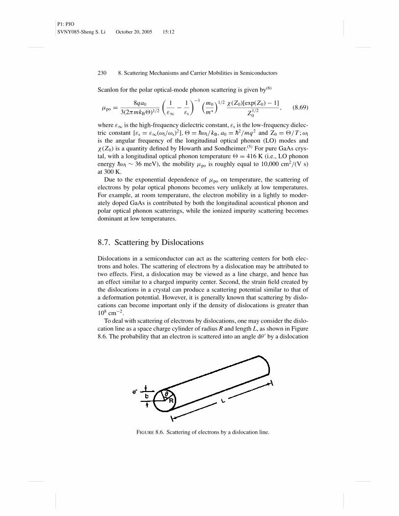
To deal with scattering of electrons by dislocations, one may consider the dislo-cation line as a space charge cylinder of radius R and length L, as shown in Figure8.6. The probability that an electron is scattered into an angle dθ ′ by a dislocation
Figure 8.6. Scattering of electrons by a dislocation line.

P1: PJO
SVNY085-Sheng S. Li October 20, 2005 15:12
8.8. Electron and Hole Mobilities in Semiconductors 231
line can be expressed by
Pd = d (b/R)
dθ ′ = 1
2sin
(θ ′
2
)(8.70)
where b is the scattering impact parameter. The differential scattering cross sectionper unit length of dislocation line charge is thus given by
σd(θ ′) = R sin
(θ ′
2
). (8.71)
The total scattering cross section can be obtained by substituting Eq. (8.71) intoEq. (8.23) and integrating over θ ′ from 0 to π , which yields
σT = 8R
3. (8.72)
Therefore, the relaxation time due to scattering of electrons by dislocations is givenby
τd = 1
NdσTv= 3
(8Nd Rv). (8.73)
The electron mobility due to scattering by dislocations can be obtained directlyfrom Eq. (8.73), which reads
µd = qτd
m∗ =(
3q
8Nd R
)1
(3m∗kBT )1/2, (8.74)
where Nd is the density of dislocation lines. Equation (8.74) shows that the electronmobility due to scattering by dislocations is directly proportional to T −1/2. Forsingle-crystal silicon and germanium the dislocation density is usually very low,and hence scattering of electrons by dislocations is negligible. It should be pointedout that scattering of carriers by dislocations could also take place by virtue of theirsurrounding strain fields. The effect of strain fields can be calculated by findinga deformation potential from the known strain field. The scattering due to thesestrain fields is usually not important for n-type semiconductors, but could becomeimportant for p-type semiconductors.
8.8. Electron and Hole Mobilities in Semiconductors
Using the relaxation time approximation and the mobility formulas derived in thischapter for different scattering mechanisms, the electron and hole mobilities in asemiconductor could in principle be calculated over a wide range of temperaturesand doping concentrations. However, one must realize that these mobility formulasare derived for the isotropic elastic scattering case. Some modifications may beneeded so that these mobility formulas can be applied to practical semiconductors.In general, it is not a simple task to fit theoretical calculations with experimentaldata for electron and hole mobilities in a semiconductor over a wide range of dopingconcentrations and temperatures because in most semiconductors the total carrier
P1: PJO
SVNY085-Sheng S. Li October 20, 2005 15:12
232 8. Scattering Mechanisms and Carrier Mobilities in Semiconductors
mobility is usually controlled by several scattering mechanisms, such as acousticalphonons, optical phonons, and ionized impurities. An exception may exist forultrapure semiconductors in which longitudinal acoustical phonon scattering mayprevail over a wide range of temperatures, and hence allows for direct comparisonbetween the theoretical calculations and measured values. In general, electronmobility in a scmiconductor due to mixed scattering processes can be calculatedby using the expression
µn = q〈τ 〉m∗
c
, (8.75)
where
1
τ=
∑i
1
τi(8.76)
and τi denotes the relaxation time due to a particular scattering process. For exam-ple, if the scattering mechanisms are due to acoustical phonons, ionized impurities,and neutral impurities, then the total scattering time constant can be obtained byemploying the reciprocal sum of the relaxation times due to these scattering pro-cesses, namely,
τ−1 = τ−1a + τ−1
l + τ−1N (8.77)
The electron mobility for the mixed scattering case can be calculated as follows:(1) finding the total relaxation time τ due to different scattering mechanisms byusing Eq. (8.76), (2) calculating the average relaxation time 〈τ 〉 from Eq. (7.57), and(3) calculating the total electron mobility by using Eq. (8.75). It should be pointedout here that computing the carrier mobility using the above procedure could bequite cumbersome if the relaxation time due to different scattering mchanismsis energy-dependent. In this case it may not be possible to obtain an analyticalexpression for the average relaxation time, and instead a numerical solution maybe needed for finding the mean relaxation time and the total carrier mobility. Onthe other hand, if the relaxation time due to different scattering mechanisms isindependent of energy, then one could use the simplified reciprocal sum formulato obtain the total electron mobility, which is given by
µ−1n =
∑i
µ−1i . (8.78)
Figure 8.7 through Figure 8.15 show the calculated and measured values of electronand hole mobilities versus temperature for pure Ge, Si, GaAs, GaP, InSb, InP, InAs,CdS, and CdTe crystals, respectively. The solid lines are theoretical calculations,while the solid dots are the measured values.(7) Figure 8.16 shows (a) the carrierconcentration versus reciprocal temperature and (b) Hall mobility versus temper-ature for the undoped (sample one) and silicon-doped (samples two to five) n-typeGaN films grown by the MOCVD technique. The symbols refer to experimentaldata. Figure 8.17 shows (a) the hole concentration versus reciprocal temperatureand (b) Hall mobility versus temperature for the Mg-doped, p-type GaN films. The
P1: PJO
SVNY085-Sheng S. Li October 20, 2005 15:12
V s
(
Figure 8.7. A comparison of the calculated drift mobility of electrons (solid curve) and themeasured Hall mobility in a pure germanium specimen. The results show that acousticalphonon scattering is the dominant scattering mechanism in this sample. After Rode,(7) p. 83,by permission.
Figure 8.8. A comparison of the calculated drift mobility of electrons (solid curve) and themeasured Hall mobility in a pure silicon specimen. The results show that acoustical phononscattering is dominated for T < 80 K, and intervalley scattering becomes comparable toacoustical phonon scattering for T ≥ 300 K. After Rode,(7) p. 81, by permission.
233
P1: PJO
SVNY085-Sheng S. Li October 20, 2005 15:12
234 8. Scattering Mechanisms and Carrier Mobilities in Semiconductors
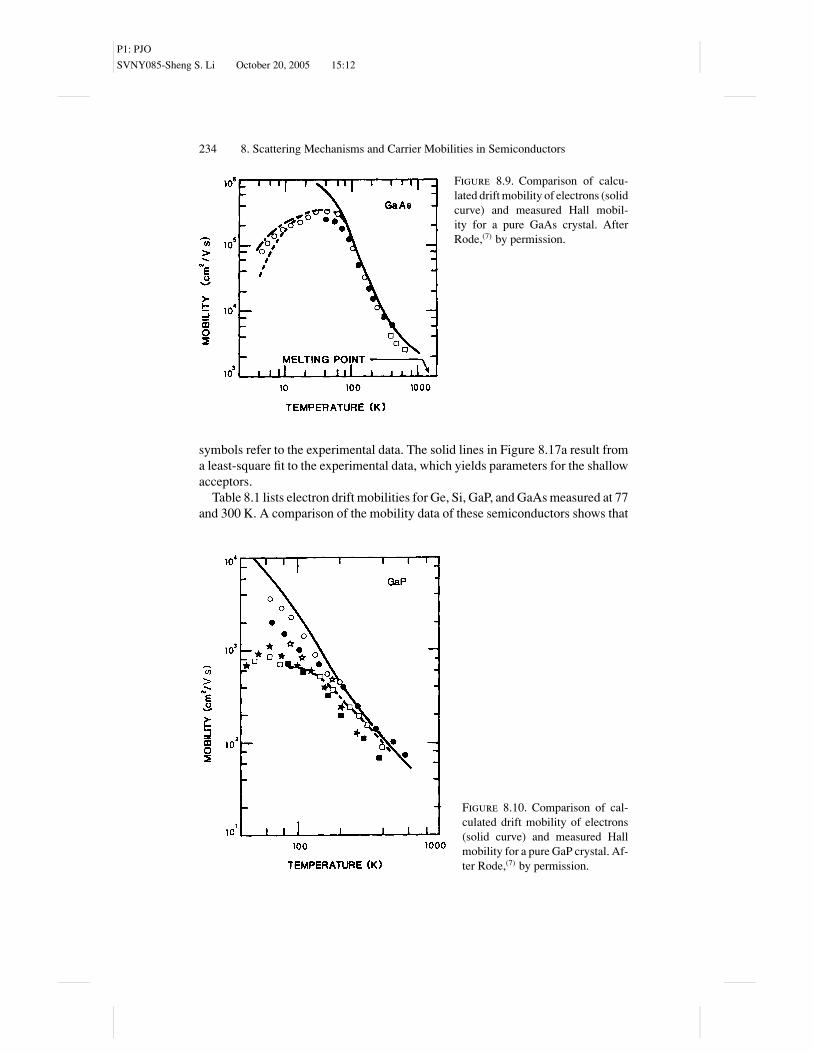
Figure 8.9. Comparison of calcu-lated drift mobility of electrons (solidcurve) and measured Hall mobil-ity for a pure GaAs crystal. AfterRode,(7) by permission.
symbols refer to the experimental data. The solid lines in Figure 8.17a result froma least-square fit to the experimental data, which yields parameters for the shallowacceptors.
Table 8.1 lists electron drift mobilities for Ge, Si, GaP, and GaAs measured at 77and 300 K. A comparison of the mobility data of these semiconductors shows that
Figure 8.10. Comparison of cal-culated drift mobility of electrons(solid curve) and measured Hallmobility for a pure GaP crystal. Af-ter Rode,(7) by permission.

P1: PJO
SVNY085-Sheng S. Li October 20, 2005 15:12
8.8. Electron and Hole Mobilities in Semiconductors 235
Figure 8.11. Comparison of calcu-lated drift mobility of electrons (solidcurve) and measured Hall mobility fora pure InSb crystal. After Rode,(7) bypermission.
InSb has the highest electron mobility, while CdS has the lowest electron mobility.In general, the electron mobilities for III-V compound semiconductors such asGaAs, InP, and InAs are higher than Si and Ge. Therefore, various electronic andphotonic devices fabricated from III-V compound semiconductors are expectedto operate at a much higher frequency and speed than that of silicon devices. Tofacilitate mobility calculations in GaAs due to various scattering mechanisms,
Figure 8.12. Comparison of cal-culated drift mobility of electrons(solid curve) and measured Hallmobility for a pure InP crystal. Af-ter Rode,(7) by permission
P1: PJO
SVNY085-Sheng S. Li October 20, 2005 15:12
236 8. Scattering Mechanisms and Carrier Mobilities in Semiconductors
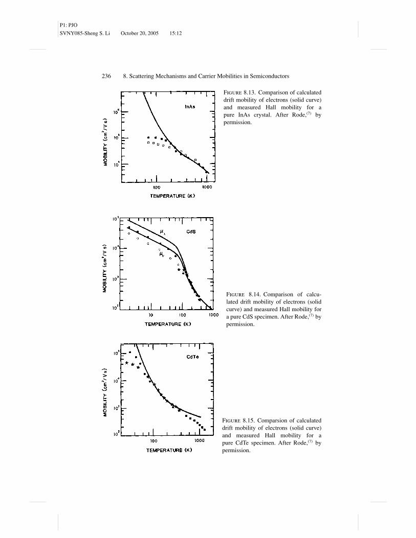
Figure 8.13. Comparison of calculateddrift mobility of electrons (solid curve)and measured Hall mobility for apure InAs crystal. After Rode,(7) bypermission.
Figure 8.14. Comparison of calcu-lated drift mobility of electrons (solidcurve) and measured Hall mobility fora pure CdS specimen. After Rode,(7) bypermission.
Figure 8.15. Comparsion of calculateddrift mobility of electrons (solid curve)and measured Hall mobility for apure CdTe specimen. After Rode,(7) bypermission.
P1: PJO
SVNY085-Sheng S. Li October 20, 2005 15:12
8.8. Electron and Hole Mobilities in Semiconductors 237
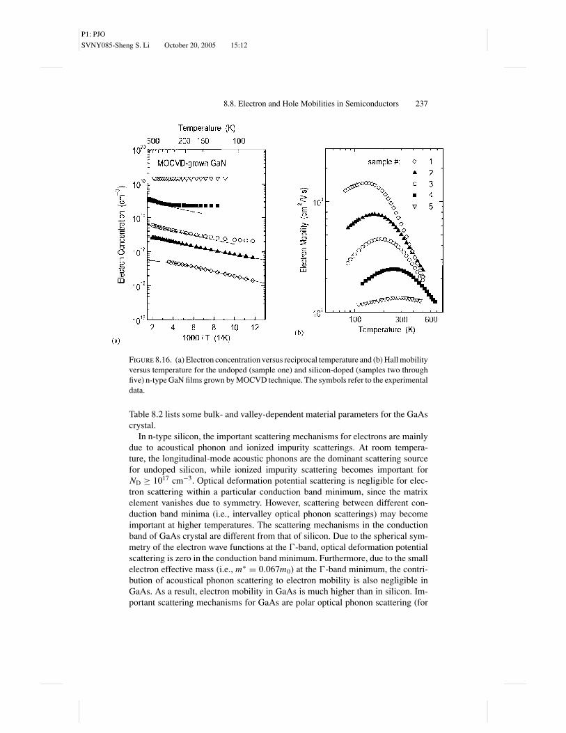
Figure 8.16. (a) Electron concentration versus reciprocal temperature and (b) Hall mobilityversus temperature for the undoped (sample one) and silicon-doped (samples two throughfive) n-type GaN films grown by MOCVD technique. The symbols refer to the experimentaldata.
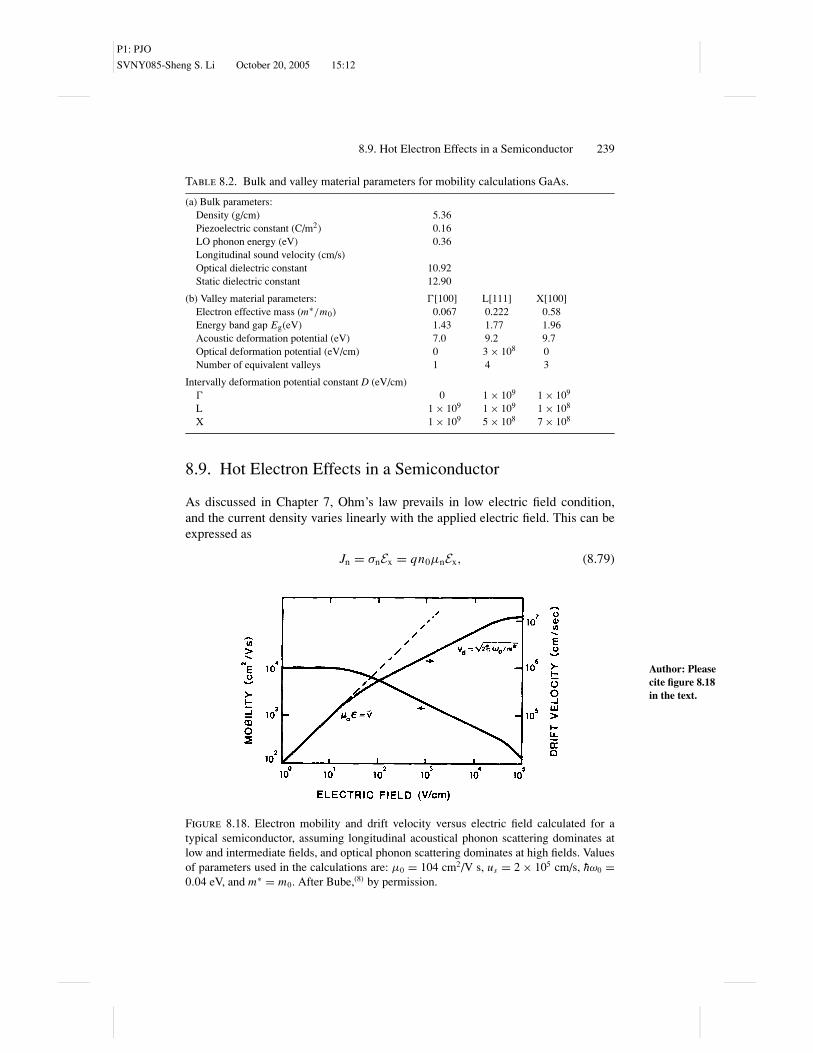
Table 8.2 lists some bulk- and valley-dependent material parameters for the GaAscrystal.
In n-type silicon, the important scattering mechanisms for electrons are mainlydue to acoustical phonon and ionized impurity scatterings. At room tempera-ture, the longitudinal-mode acoustic phonons are the dominant scattering sourcefor undoped silicon, while ionized impurity scattering becomes important forND ≥ 1017 cm−3. Optical deformation potential scattering is negligible for elec-tron scattering within a particular conduction band minimum, since the matrixelement vanishes due to symmetry. However, scattering between different con-duction band minima (i.e., intervalley optical phonon scatterings) may becomeimportant at higher temperatures. The scattering mechanisms in the conductionband of GaAs crystal are different from that of silicon. Due to the spherical sym-metry of the electron wave functions at the �-band, optical deformation potentialscattering is zero in the conduction band minimum. Furthermore, due to the smallelectron effective mass (i.e., m∗ = 0.067m0) at the �-band minimum, the contri-bution of acoustical phonon scattering to electron mobility is also negligible inGaAs. As a result, electron mobility in GaAs is much higher than in silicon. Im-portant scattering mechanisms for GaAs are polar optical phonon scattering (for

P1: PJO
SVNY085-Sheng S. Li October 20, 2005 15:12
238 8. Scattering Mechanisms and Carrier Mobilities in Semiconductors
(a) (b)
Figure 8.17. (a) Hole concentration versus reciprocal temperature and (b) Hall mobilityversus temperature for Mg-doped, p-type GaN films. The symbols refer to the experimentaldata. The solid lines in (a) are a least-square fit to the experimental data, which yieldsparameters for shallow acceptors.
pure and lightly doped GaAs), ionized impurity scattering (for ND ≥ 1017 cm−3),and intervalley optical phonon scattering (at high fields).
For p-type silicon and GaAs, the valence band maxima for both silicon and GaAsare located at the �-point (i.e., the zone center), and wave functions of holes donot possess spherical symmetry. Thus, optical deformation potential scattering isimportant for holes in p-type GaAs. In addition, both acoustical phonon scatteringand ionized impurity scattering may also play an important role in the valencebands for both materials.
Table 8.1. Electron Drift Mobilities µn(cm2/Vs) for Ge, Si, GaP,and GaAs.
Ge Si GaP GaAs
T = 300 K
Calculated 4080 1580 183 8920Measured 3800–4200 1350–1450 120–200 3500–9000
T = 77 K
Calculated 37,400 22,800 4370 2.9 × 10⁵
Measured 35,000–47,000 18,000–24,000 2.2 × 10⁵
P1: PJO
SVNY085-Sheng S. Li October 20, 2005 15:12
8.9. Hot Electron Effects in a Semiconductor 239
Table 8.2. Bulk and valley material parameters for mobility calculations GaAs.
(a) Bulk parameters:Density (g/cm) 5.36Piezoelectric constant (C/m2) 0.16LO phonon energy (eV) 0.36Longitudinal sound velocity (cm/s)Optical dielectric constant 10.92Static dielectric constant 12.90
(b) Valley material parameters: �[100] L[111] X[100]Electron effective mass (m∗/m0) 0.067 0.222 0.58Energy band gap Eg(eV) 1.43 1.77 1.96Acoustic deformation potential (eV) 7.0 9.2 9.7Optical deformation potential (eV/cm) 0 3 × 10⁸ 0Number of equivalent valleys 1 4 3
Intervally deformation potential constant D (eV/cm)� 0 1 × 10⁹ 1 × 10⁹
L 1 × 10⁹ 1 × 10⁹ 1 × 108
X 1 × 109 5 × 10⁸ 7 × 10⁸
8.9. Hot Electron Effects in a Semiconductor
As discussed in Chapter 7, Ohm’s law prevails in low electric field condition,and the current density varies linearly with the applied electric field. This can beexpressed as
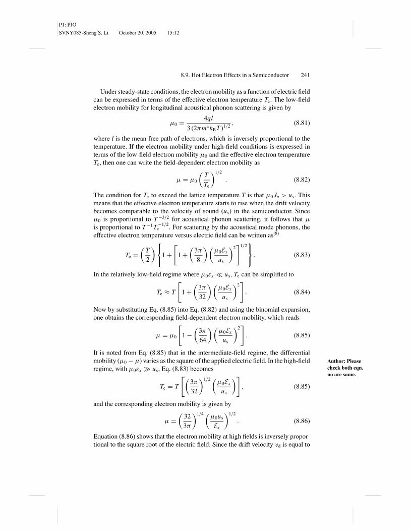
Author: Pleasecite figure 8.18in the text.
Jn = σnEx = qn0µnEx, (8.79)
Figure 8.18. Electron mobility and drift velocity versus electric field calculated for atypical semiconductor, assuming longitudinal acoustical phonon scattering dominates atlow and intermediate fields, and optical phonon scattering dominates at high fields. Valuesof parameters used in the calculations are: µ0 = 104 cm2/V s, us = 2 × 105 cm/s, h--ω0 =0.04 eV, and m∗ = m0. After Bube,(8) by permission.

P1: PJO
SVNY085-Sheng S. Li October 20, 2005 15:12
240 8. Scattering Mechanisms and Carrier Mobilities in Semiconductors
where σn is the electrical conductivity, and Ex is the applied electric field. As theelectric field continues to increase, a point is reached at which the electric currentdensity will no longer vary linearly with the electric field. This means that either theelectron density or the electron mobility becomes a function of the electric field. Anincrease in the electron density is possible if the electric field is high enough to cause(1) impact ionization (i.e., ionization of other imperfections or crystal atoms uponimpact by hot electrons), (2) field ionization (i.e., ionization of imperfections byquantum mechanical tunneling to the nearest band), or (3) electrical injection (i.e.,injection of electrons from contacts into the semiconductor). These processes maylead to a change of electric current with applied electric field that is faster than thatpredicted by Eq. (8.79). It will be shown later that these effects are usually observedin a p-n junction diode operating under a large reverse bias condition. Another high-field effect, which has been found in many III-V compound semiconductor devices,is that the electric current density will increase with the electric field at a slowerrate than that predicted by Eq. (8.79) under high-field condition. This effect arisesfrom the decrease in electron mobility with increasing electric field resulting fromscattering of electrons by optical phonons under high electric field conditions.
In this section, only the effect of applied electric fields on electron mobility isconsidered. The mobility versus electric field relation can be derived by assumingthat the scattering of electrons is dominated by the longitudinal-mode acousticalphonons.
It is generally known that as the electric field increases, the electrons will gainenergy from the applied electric field. Furthermore, scattering of electrons is as-sociated with the absorption or emission of phonons. Thus, in order to calculateenergy loss by electrons due to phonon scattering, it is necessary to determine theaverage energy resulting from either absorption or emission of phonons under highelectric field conditions. The electron energy will increase if there is a net gain inenergy due to phonon absorption.
Under high electric field conditions, electron energy can be described in termsof an effective electron temperature, Te. For a nondegenerate semiconductor, anincrease in energy of the order of kBT represents a large change in the mean electronenergy. An effective electron temperature Te for such an energetic electron maybe defined by the Maxwellian mean velocity, which is given by
〈v〉 =(
kBTe
8πm∗
)1/2
. (8.80)
If the effective electron temperature defined by Eq. (8.80) is equal to the latticetemperature, then the electron mobility is independent of the electric field. On theother hand, if there is a net gain of energy due to the effects of applied electricfield and acoustical phonon scattering, then the electrons will heat up. Under thiscondition, Te becomes larger than the lattice temperature of the crystal, and theelectric current will no longer vary linearly with the electric field. Derivation of thecurrent–electric field relation under high–field conditions is quite complicated, andonly the relation between the electron mobility and the electric field is discussedin this section.
P1: PJO
SVNY085-Sheng S. Li October 20, 2005 15:12
8.9. Hot Electron Effects in a Semiconductor 241
Under steady-state conditions, the electron mobility as a function of electric fieldcan be expressed in terms of the effective electron temperature Te. The low-fieldelectron mobility for longitudinal acoustical phonon scattering is given by
µ0 = 4ql
3 (2πm∗kBT )1/2 , (8.81)
where l is the mean free path of electrons, which is inversely proportional to thetemperature. If the electron mobility under high-field conditions is expressed interms of the low-field electron mobility µ0 and the effective electron temperatureTe, then one can write the field-dependent electron mobility as
µ = µ0
(T
Te
)1/2
. (8.82)
The condition for Te to exceed the lattice temperature T is that µ0 Jn > us. Thismeans that the effective electron temperature starts to rise when the drift velocitybecomes comparable to the velocity of sound (us) in the semiconductor. Sinceµ0 is proportional to T −3/2 for acoustical phonon scattering, it follows that µ
is proportional to T −1T −1/2e . For scattering by the acoustical mode phonons, the
effective electron temperature versus electric field can be written as(8)
Te =(
T
2
) 1 +
[1 +
(3π
8
) (µ0Ex
us
)2]1/2
. (8.83)
In the relatively low-field regime where µ0εx � us, Te can be simplified to
Te ≈ T
[1 +
(3π
32
) (µ0Ex
us
)2]
. (8.84)
Now by substituting Eq. (8.85) into Eq. (8.82) and using the binomial expansion,one obtains the corresponding field-dependent electron mobility, which reads
µ = µ0
[1 −
(3π
64
) (µ0Ex
us
)2]
. (8.85)
It is noted from Eq. (8.85) that in the intermediate-field regime, the differentialmobility (µ0 − µ) varies as the square of the applied electric field. In the high-field Author: Please
check both eqn.no are same.
regime, with µ0εx � us, Eq. (8.83) becomes
Te = T
[(3π
32
)1/2 (µ0Ex
us
)], (8.85)
and the corresponding electron mobility is given by
µ =(
32
3π
)1/4 (µ0us
Ex
)1/2
. (8.86)
Equation (8.86) shows that the electron mobility at high fields is inversely propor-tional to the square root of the electric field. Since the drift velocity vd is equal to
P1: PJO
SVNY085-Sheng S. Li October 20, 2005 15:12
242 8. Scattering Mechanisms and Carrier Mobilities in Semiconductors
the product of electron mobility and electric field, it will increase with the squareroot of the electric field at high fields.
It should be noted that the results obtained above are for the case when scat-tering of electrons is due to longitudinal acoustical phonons. For such scattering,increasing electron energy with the applied electric field will result in an increaseof phonon scattering, which in turn will lead to the reduction of electron mobilitywith increasing electric field. On the other hand, if scattering is dominated by theionized impurity scattering, then an increase in electron energy with increasingelectric field will result in an increase of electron mobility. This is due to the factthat, for ionized impurity scattering, the probability of scattering decreases withincreasing electron energy (i.e., τ−1
I ∼ E−3/2).Figure 8.16 shows a plot of electron mobility and drift velocity versus elec-
tric field calculated for a typical semiconductor at 300 K.(2) In this figure, it isassumed that scattering of electrons is dominated by the longitudinal-mode acous-tical phonons at low and intermediate electric fields and by optical-mode phononsat high electric fields. The results clearly show that, for scattering by acousticalphonons, the electron mobility will decrease with the square of the applied elec-tric fields, and the high-field electron mobility will vary inversely with the squareroot of the electric fields. At very high fields hot electrons will start interactingwith optical phonons, which in turn would limit the drift velocity to a saturationvalue.
The most widely used method to study the hot electron effects in a semicon-ductor is the Monte Carlo approach. It consists of a simulation of the motion ofone or more electrons inside a semiconductor subject to the action of an exter-nal applied electric field and given scattering mechanisms. The basic principle ofthe Monte Carlo method relies on the generation of a sequence of random num-bers with given distribution probabilities. When charge transport is analyzed onsubmicrometer scales under very high electric field conditions, the conventionalsemiclassical approach of transport processes in terms of the Boltzmann equationcan be substituted by a full quantum mechanical description, namely, the MonteCarlo approach.
A brief description of the general procedure governing the Monte Carlo methodis given as follows: Consider the case of a cubic semiconductor under a very highelectric field Ex . The simulation starts with a set of given initial conditions withinitial wave vector k0. The duration of the first free flight is determined stochasti-cally from a probability distribution determined by the scattering probabilities. Thesimulation of all quantities of interest, such as velocity and energy, are recorded.A dominant scattering mechanism is then selected as being responsible for the endof the free flight according to the relative probabilities of all possible scatteringmechanisms. From the transition rate of this scattering mechanism, a new wavevector, k, value after scattering is determined stochastically as the initial state ofthe new free flight, and the entire process is repeated iteratively. The results ofthe calculation become more and more accurate as the simulation ends when thequantities of interest are known with the desired precision. A detailed descriptionof this method can be found in a monograph edited by Reggiani.(9) The Monte
P1: PJO
SVNY085-Sheng S. Li October 20, 2005 15:12
8.9. Hot Electron Effects in a Semiconductor 243
Carlo method allows one to extract derived phyical information from simulatedexperiments, and is a powerful tool for analyzing stationary and transient transporteffects in semiconductors under high-field conditions. It is particularly useful foranalyzing high-field transport properties in submicron devices.
Problems
8.1. Using Eqs. (8.18), (8.19), and (8.20) derive Eq. (8.21), assuming that vk =vk, k = k ′, and d3k ′ = k ′2 sin θ ′dθ ′dφ′dk ′.
8.2. Using the Conwell–Weisskopf model, derive Eqs. (8.37) and (8.38) (i.e.,V (r ) = q/4πε0εsr for ionized impurity scattering).
8.3. Show that the maximum change of electron energy due to the acousticalphonon scattering is given by Eq. (8.43). Does this satisfy the condition ofelastic scattering?
8.4. Calculate the Debye screen lengths for Si, Ge, and GaAs for ND = 1015, 1017,and 1019 cm−3. Given εs = 11.7 for Si, 12 for GaAs, and 16 for Ge.
8.5. If the electron mobility in silicon is due to scattering of acoustical phononsand ionized impurities, show that the mixed scattering mobility can be ap-proximated by
µL I = µL
{1 + χ2
[Ci (χ ) cos χ + sin χ
(Si (χ ) − π
2
)]},
where χ2 = 6µL/µL, and µL and µI are the acoustical phonon scattering andionized impurity scattering mobilities; Ci(χ ) and Si(χ ) are the cosine and sineintegrals of χ , respectively. (See the paper by P. P. Debye and E. M. Conwell,Phys. Rev. 93, 693 (1954).)
8.6. Using Eq. (8.58), calculate the electron mobility due to acoustical phononscattering for pure silicon when 100 ≥ T ≤ 300K. Given (m0/m∗)5/2 =20.4, Ec1 = 12.8 eV, and Mu2
s = 1.97 × 10¹² dynes/cm2.8.7. Using the expression for τI given by Eq. (8.35) and µI = q〈τI〉/m∗, show that
the ionized impurity scattering mobility is given by Eq. (8.36).8.8. The inverse scattering relaxation time for piezoelectric scattering in a nonde-
generate semiconductor with a parabolic band is given by
τ−lpe = 3q2κT P2m∗d
6πh--3ε0k ′ ,
where k ′ is the electron wave vector and P is the piezoelectric coefficient.Derive an expression for the piezoelectric scattering mobility, and show thatthe mobility is proportional to T 1/2.
8.9. For a GaAs crystal, the polar optical phonon scattering mobility µp0 given byEq. (8.69) can be simplified to
µpo = 5.3 × 10³
(χ (Z0)
[exp (Z0) − 1
]Z1/2
0
),
P1: PJO
SVNY085-Sheng S. Li October 20, 2005 15:12
244 8. Scattering Mechanisms and Carrier Mobilities in Semiconductors
where �, h--ωl/kB, a0 = h--2/mq2, and Z0 = �/T ; ωl is the angular frequency ofthe longitudinal optical modes, and χ (Z0) is a quantity defined by Howarth andSondheimer.(5) For pure GaAs, the longitudinal optical phonon temperature � isequal to 416 K (i.e., the LO phonon energy h--ωl ∼ 36 meV), and µp0 ≈ 10, 000cm2/(V s) at 300 K.
The ionized impurity scattering mobility, µi, is given by
µi = 1.5 × 10¹⁸
NI[ln(1 + b) − b/(1 + b)]T 3/2,
where
b = 9.1 × 10¹³
n0T 2.
The piezoelectric scattering mobility is given by
µpz = 4.89 × 10⁵
(100
T
)1/2
.
Assuming that Matthiessen’s rule prevails, the total electron mobility for this GaAscrystal can be approximated by
µ−1n = µ−1
po + µ−1i + µ−1
pz
Using the above expression, plot the electron mobility versus temperature for thisGaAs crystal for 100 < T < 600 K for NI = 1016, 1017, and 1018 cm−3.
References
1. E. M. Conwell and V. F. Weisskopf, Phys. Rev. 77, 388–390 (1950).2. H. Brooks, in: Advances in Electronics and Electron Physics (L. Marton, ed.), Vol. 7,
Academic Press, New York (1955), pp. 85–182.3. C. Erginsoy, Phys. Rev. 1013–1017 (1956).4. J. Bardeen and W. Shockley, Phys. Rev. 80, 72–84 (1950).5. D. Howarth and E. Sondheimer, Proc. R. Soc. Lond. Ser. A 219, 53 (1953).6. R. L. Petritz and W. W Scanlon, Phys. Rev. 97, 1620 (1955).7. D. L. Rode, in: Semiconductors and Semimetals (R. K. Willardson and A. C. Beer, eds.),
Vol. 10, Academic Press, New York (1975).8. R. H. Bube, Electronic Properties of Crystalline Solids, Chapter 8, Academic Press, New
York (1974) p. 289.9. R. Reggiani, Hot Electron Transport in Semiconductors, Springer-Verlag, New York
(1985).
Bibliography
F. J. Blatt, Physics of Electronic Conduction in Solids, McGraw-Hill, New York (1968).C. Herrings and E. Vogt, “Transport and Deformation Potential Theory for Many-Valley
Semiconductors with Anisotropic Scattering,” Phys. Rev. 101, 944–961 (1956).

P1: PJO
SVNY085-Sheng S. Li October 20, 2005 15:12
8.9. Hot Electron Effects in a Semiconductor 245
S. S. Li, The Dopant Density and Temperature Dependence of Electron Mobility and Re-sistivity in n-type Silicon, NBS Special Publication, (1977), pp. 400–433.
S. S. Li, The Dopant Density and Temperature Dependence of Hole Mobility and Resistivityin p-type Silicon, NBS Special Publication (1979), pp. 400–447.
K. Seeger, Semiconductor Physics, Springer-Verlag, New York (1973).