Embed Size (px)
Citation preview

OCTOBER TO DECEMBER 1988 VOL. 13 NO. 4
SCIENTIFIC .) %
INFORMATION ,, _BULLETINDEPARTMENT OF THE NAVY OFFICE OF NAVAL RESEARCH FAR EASTDEPARTMENT OF THE AIR FORCE OFFICE OF SCIENTIFIC RESEARCH FAR EASTUNITED STATES ARMY RESEARCH OFFICE FAR EAST
Co
0. W
N J~. .,*
DTIC'Mi.LECTEFEB 0 198 3D
D
APPROVED FOR PUBLIC RELEASE: DISTRIBUTION UNLIMITED NAVSO P-358089 2 6 149
UNCLASSIFIED 77,ECR:'v C,'ISS. -C; 71O O; _-'S ; AG_
REPORT DOCUMENTATION PAGE
'a REPORT S:C RiTY C.ASS FiCAT;ON lb RESTRICTIVE MARKINGS
2a SECR:T' CLASS -CAT ON A7---TY 3 DiSTRiBuTjON AVAILABILITY OF REPORT
'o DtCASS LCATON DO'rGRAD.NG SCIEDuLE APPROVED FOR PUBLIC RELEASE;DISTRIBUTION UNLItITED.
4 P;EPOR%' NG OPAN,ZA ,-ON PE ORT \MBER'S) S MONITORING ORGANIZATION REPORT NUMBER(S)
ONRFE Vol 13, No. 46a %AME O P:R%'fNG ORGAN.ZAT'ON 6o O;FiCE SYMBOL 7a NAME OF MONITORING ORGANIZATION
ON RIA FOSRARO j (If applicable)
6c ADDRESS City, State, and ZIP Code) 7b ADDRESS (City, State, and ZIP Code)
Liaison Office, Far EastAPO San Francisco 96503-0007
Sa NAME OF :-'.DING/SPO%SOR;NG 8 OFFiCE SYMBOL 9 PROCUREMENT INSTRUMENT IDENTIFICATION NUMBERORGAN;ZA ON (If applicable)
8c ADDRESS(City, State, and ZIPCode) 10 SOURCE OF FUNDING NUMBERS
PROGRAM PROJECT TASK WORK UNITELEMENT NO. NO NO ACCESSION NO
11 ITL.E (Include Security Classification)
ONR FAR EAST SCIENTIFIC INFORMIATION BULLETIN12 :-PSONA- AUTHOR(S)Arthur F. Findeis, Director; Sandy Kawano, Editor
13a TYPE O REPORT 13b TIME COVERED 14. DATE OF REPORT (Year, Month, Day) 1S PAGE COUNTI FROM TO October-December 1988
16 SUPPLEMENTARY NOTATION
ISSN: 0271-7077
17 COSATi CODES 18 SUBJECT TERMS (Continue on reverse if necessary and identify by block number)
FIELD GROUP SUB-GROuP Japan Doping Air-sea interactionSuperconductors Band theory Single crystal filmsOceanography Mott transition Metallic multilayers
'9 ABSTPACT (Continue on reverse if necessary and identify by block number)This is a quarterly publication presenting articles covering recent developments in Far
Eastern (particularly Japanese) scientific research. It is hoped that these reports (whichdo not constitute part of the scientific literature) will prove to be of value to scientistsby providing items of interest well in advance of the usual scientific publications. Thearticles are oritten primarily by members of the staff of ONR Far East, the Air Force Officeof Scientific Research, and the Army Research Office, with certain reports also beingcontributed by visiting stateside scientists. Occasionally, a regional scientist will beinvited to submit an article covering his own work, considered to be of special interest.This publication is approved for official dissemination of technical and scientific informa-tion of interest to the Defense research community and the scientific community at large.
Subscription requests to the Scientific Information Bulletin should be directed to theSuperintendent of Documents, Attn: Subscription, Government Printing Office, Washington, DC20402. The annual subscription charge is: domestic, $11.00; foreign, $13.75. Cost for asingle copy is: domestic, $7.0; foreign, 8-7-.20 DISTR!BuTiON / AVAILABILITY OF ABSTRACT 21 ABSTRACT SECURITY CLASSIFICATION
E]'JNCLASS:FIED/UNLIMITED 0 SAME AS RPT E DTIC USERS
22a NAME OF RESPONSIBLE INDIVIDUAL 22b TELEPHONE (include Area Code) 22c OFFICE SYMBOL
DD FORM 1473, 84 MAR 83 APR editon may be used until exhausted SECURITY CLASSIFICATION OF THIS PAGEAll other editions are obsolete UNCLASS F F TEU
i ,

18. Subject Terms (continued)
Superconducting thin films Film growth by evaporationFilm growth by sputtering Superconducting propertiesTechnology transfer techniques SiC coatings researchChemical vapor deposition Metallic superlatticesSuperconducting synchrotron Kuroshio Current researchNeutron scattering Hubbard modelThomas-Fermi screening MagnetiteSupercomputers Computational fluid dynamicsBi omateri al s
ID
ii

CONTENTS
Page
High-Temperature Superconducting. Thin Films in Japan. ..................Michael Osofsky, Phillip R. Broussard, and Earl Callen
The fundamentals of high temperature superconducting thin filmsare reviewed, and the facilities and programs of several Japanesesuperconducting thin filn groups are described.
Research Institute for Metal Surface of High Performance (RIMES):.An Example of Japanese Transfer of Technology Techniques . ........ 25
Fred Pettit
Governmental leadership coupled with the enthusiasticparticipation of industry and academia are important characteristicsof this technology tanw fer pwcess.
Research and Applications of Metallic Superlattices, High T, Superconductors,X-Ray Optics, and Compact Synchrotrons ............................ 31
Charles M. Falco
This article describes research on metallic superlattices, high TCsuperconductors, and x-ray optics and also reports on thedevelopment of compact synchrotrons for generation of soft-x- rays.
Kuroshio Exploitation and Utilization Research (KER) ..................... 39Wayne V. Burt
This article discusses the various KER research projects initiated tounderstand and clarify the mechanisms and characteristics of theKuroshio Current.
What Is Going on in the La2CuO Superconductors? .,.............. 43Earl Callen
Progress in superconducting ceramics requires understandinginterrelated systems of oxide superconductors. The La2CuO'
superconductors may be the primary host for allthe high TC Cu oxidesso far discovered.
ONRFE SCI INFO BUL 13 (4) 88 iii

Page
Current Japanese Supercomputers for ComputationalFluid D ynam ics A pplications ...................................................................................... 61
Hideo Yoshihara
Current top-of-the-line Japanese supercomputers are described,stressing the vector features significant for highly vectorizedcomputational fluid dynamics codes.
International Symposium on Strategy of Innovation inM aterials Processing (SIM AP '88) , .......................................................................... 69
E.A. Metzbower
The six sessions of the symposium described in this article reflect thedepth and breadth of the research efforts at the Welding ResearchInstitute at Osaka University.
International M eetings in the Far East, 1989-1994 ........................................................ 75Yuko Ushino
Index ........................................................ 89
Cover: This issue features a photographic reproduction of a fishprint. The Japanese call it"gyotaku," which is a phonetic rendering of two Chinese characters, or kanji: gyo, meaning fish,and taku, meaning print. In a way this printmaking is similar to brass rubbing or tombstonerubbing: a sheet of pliable paper is spread over the object; molded to the contours by light fingerpressure; and surface shaded or rubbed by soft pencil, charcoal, or crayon. Anglers initiatedthis custom as a means of recording their prize catches. Gyotaku is uniquely Japanese, beingdeveloped and recognized in Japan. In 1955 an association was formed to exhibit and promotethis as an art form. Some of the first works exhibited outside Japan were displayed in June 1956at the American Museum of Natural History. Courtesy of E.M. Lenoe.
ONRFE SCI INFO BUL 13 (4) 88 iv

HIGH TEMPERATURE SUPERCONDUCTING
THIN FILMS IN JAPAN
Michael Osofsky, Phillip R. Broussard, and Earl Callen
T he study of thin films of the new high In this article we sketch some of the basicstemperature superconductors can of film growth and then describe activities,
address a wide range of scientific questions facilities, and programs at several Japaneseand may well lead to many vital technolog- laboratories--Kyoto University, the Nipponical applications. We review the fundamen- Telephone and Telegraph (NIT) Electricaltals of high temperature superconducting Communications Laboratory at Ibaraki, thethin films: theirstructure, how theirphysical National Research Institute for Metals atand superconducting properties are charac- Tsukuba, the Electrotechnical Laboratoryterized, and how they are made. We then atTsukuba, Sumitomo ElectricCompany indescribe facilities and programs of several Itami City, Osaka University, andJapanese superconducting thinfilm groups. Matsushita Electric Company in Osaka.
THIN FILM TECHNOLOGYINTRODUCTION
StructureOne of the most sought after com-
mercializations of the new high tempera- The structures of the high tempera-ture superconductors will be in electronics-- ture superconducting compounds aredetectors, switches, logic de,, ices, intercon- related to the barium titanate or simplenects, and mixers. Some of these applica- perovskite unit cell (Figure 1). In this struc-tions can be realized with pure supercon- ture oxygen atoms, in an octahedral config-ducting elements. Others will be hybrid uration, surround a metal ion that is at thesemiconductor-superconductor devices, center of a cube of cations. Figure 2 showsinterfacing the new materials with silicon or the structures of several of the new super-with gallium arsenide. Thin superconduct- conductors. Key components are copper-ing films deposited onto a passive substrate, oxygen sheets separated by other cations.onto a semiconducting device, or on anintermediate buffer layer are a natural way Growth of Superconducting Thin Filmsto achieve this goal. Factors such as filmstoichiometry, crystalline orientation, We will concentrate on two tech-homogeneity, surface smoothness, and niques, evaporation and sputtering (Ref 1),substrate interaction impact on these appli- which produce films less than or equal tocations and must b,. optimized. Many 1 pm thick. Both techniques deposit atomsJapanese laboratories have considerable of the desired compound onto hot or coldexperience in both semiconducting and substrates and may include a postevapora-superconducting thin film technologywhich tion anneal. The process must achievethey are exploiting in high T, development, uniform and correct composition, crystal
ONRFE SCI INFO BUL 13 (4) 88 1

structure, and oxygen content throughout films must still be postannealed. Epitaxialthe entire filmwhile avoiding reactionswith films grown in this manner have the bestthe substrate. superconducting properties. One problem
with this technique is that the introduction
of oxygen into deposition systems redtcesthe operating life of heaters and filaments.Deposition onto a substrate at ambienttemperature and low oxygen partial pres-sure (10' to 106 Torr) produces insulating,amorphous films that must be postannealedin oxygen to achieve superconducting prop-erties.
We will give only generic descrip-tions of growth techniques aiid will notdescribe annealing schedules since thereare as many procedures as there are
0 Cation research groups.
Evaporation. In general, filmMetal growth by evaporation use,,, separate
sources for each element to avoid preferen-Figure 1. The simple perovskitce (or tial evaporation of the higher vapor pres-
barium titanatc) unit celi.
Oxygen atoms arc sure species (Figure 3). The rates of allpositioned at the vertices sources must be monitored and preciselyof the octahedron. controlled to produce stoichiometric con-
positions. This is accomplished through theThe most commonly used substrates use of quartz cry:stal rate monitors in a
are single crystals of strontium titanate feedback control loop. The two most corn-(SrTiO 3), magnesium oxide (MgO), and monly used evaporation sources are resis-yttria-stabilized zirconia (YSZ). These tively heated "ovens" (Knudsen cells orcompounds are cubic with lattice param- "K-cells") and electron beam sourceseters of 3.905, 4.203, and 5.16 A, respec- (e-guns). In resistively heated sources largetively, and do not detrimentally interact electric currents heat a filament that sur-with the superconductors. Films have been rounds a container filled with the material.made on other materials such as sapphire, E-guns heat the material via a focused elec-lithium niobate, and even silicon, but they tron beam. The beam rasters across theare plagued by substrate interaction prob- target to prevent pits from developing andlems. modulating the evaporation rate. Gener-
Deposition onto a hot substrate allye-gunsareusedonlowervaporpressure(usually 600 °C and above) in the presence materials and thermal sources for the highof oxygen (partial pressures up to I mTorr) vapor pressure materials.can produce in-situ growth of the supercon-ducting phase. At present many of these
ONRFE SCI INFO BUL 13 (4) 88 2

Sputtering. In the sputtering process has the advantage that a composite target(Figure 4) a target under bombardment by can be used, which removes the need forions of a plasma (usually argon) ejects active rate control during deposition. Somematerial that deposits onto asubstrate. The systems use multiple sputter-guns in atarget composition usually deviates from manner analogous to the evaporation con-the desired film composition. The amount figurationbutwith much better rate control.of this deviation, peculiar to each system, In addition, adding oxygen to the sputteringmust be discovered by trial and error. The gas is a natural way to enhance the oxidationplasma is excited either by rf radiation or a of the film during deposition. However,large dc potential difference. The process is some oxygen becomes negatively ionizedusually aided by the placement of magnets and bombards the substrate, which resput-
to confine electrons near the target (so- ters film components.called magnetron sputtering). Sputtering
- Cu
- )La/Sr -Cu
* - La/Sr -B
-CU
La/Sr * 0% )C,;0
La/Sr Ba
-Cu - Cu
La2 Sr CuO YBa2Cu 3 7
Tetragonal (14/mmm) Orthorhombic (Pmmm)a = 3.7873(1), c = i3.2883(3) a = 3.8185(4), b = 3.8856(3),
c = 11.6804(7)
Figure 2. The structure of several of the high temperature superconductors: La2,SrCuO4, with T, 40 K(x = 0.15); YBa2Cu3O, with T. = 95 K; Bi2Sr 2 CaCu2O8, with T, = 85 K; TI2Ba 2CaCu20, with
T = 85 K; TI2Ba 2Ca 2Cu 30 0, with T = 110 K. There is also a Bi2Sr2Ca2Cu 3O 0 , with structure similar
to the TI compound and Tc -110 K. The unshaded circles represent oxygen atoms.
ONRFE SCI INFO BUL 13 (4) 88 3

Jill if lIlillllll II
, • •# ) .
* * rI I I 1 I ? : Vt ' . j ( j
69 00
~1
0 cN
0 Q
P •. o 0.
.
ONRFE SCI NFO BUIL 13 (4) 88

4- Hokide Ctol or abt)no macroscopic properties, and show corn-S~bs~fateplete magnetic flux expuls Ion (Meissner
effect) below the transition. On the otherhand, if the film is to be used as an infrared
Rate Montr rdictin thin ri must be polycrystal-
ducingthi fims anbe divided into twobodinterrelated categories: materials
properties and superconducting properties.K-cell e-gun Obviously, materials properties strongly
Figue 3 Scemaic f athi fim C'iloraioninfluence the Superconducting characteris-
svstcmr with C-guin and K-cc II sources.tisothflmHigh 1' svkNstm, typically have three'O u rcc s Materials Properties. The inipor-
tant materials properties of thin films ate
.--- IC ~' ~ ~ ~cation compos itioi, oxygen content, hotiio-genit. ryta structure, alignment, and
gross morphology T[he most common toolsEjected Target Material used to ;iaye hs properties are optical
/r and 0 Ions mcooptransmission adsann
j]Argon Ion electron microscopy (TEM and SEM),energy dispersive spectroscopy (EDS),
Target-~ microprobe analysis, and x-ray diffractionR~orOC(XRD).
MagnetsOptical microscopy with polarizedlight efficiently provides i simple picture of
Fiizurc 4. Schcmaic of it ingic-larliet spult il rg the gross morphology of a film, withs~IrnI micron spatial resolution. One can
reidily observe the average grain size. the
Characterization fraction of extraneous phases, orientationsof the grains,, and the presence of large
What is a "good" film? The answer defect structures Such w twins. Figure 5depends on the film's intended application, shows a poiariied light micrograph of aIf oric wvarts to s~tudy] the properties of the patterned NYiaCuO, film. We can see the
suprcoducortheni a g~ood film hias the general teXtujre of the film: grain orienta-
right stoichiometr-v and oxygen content and tion, grain alignment, and grain size. Inis an epitaxial single crystal with the correct addition, thouIgh not shown in this black and
ONRFEi SC!I INFO BLWL 13 (4) 885

Figurc 5. Polarized light micrograph of a pattcrncdYBau2 CO 7 film magnificd 1,000 times.
SEM shows details on scales from a order to identify the constituents (and theirfew microns down to 1,000 A, while TEM homogeneity) on micron length scales.can resolve features down to 2 A. Figure 6 Figure 7 shows the SEM image of a film ofis an SEM micrograph of the film in Bi-Sr-Ca-Cu-O. By a bismuth dot map oneFigure 5. The greater detail shows that the can reveal the relative concentrations of thealigned and oriented grains form a network constituent elements on the film surface.throughout the film. This network makes it X-ray diffraction is the standarddifficult to precisely determine the film's method for identifying crystal structure andresistivity and critical current density. grain orientation. A diffraction event con-
When an electron beam bombards a sists of two pieces of information that relatematerial, x rays with energies characteristic to the crystal structure: the angle at whichof the constituent elementsare excited. The it occurs and how intense it is. The formerelectron microprobe and the EDS feature provides information about the lattice--itsof electron microscopy detect the energies symmetry and unit cell parameters. Theand wavelengths of the emitted radiation in latter can be analyzed in terms of the
ONRFE SCI INFO BIL 13 (4) 88 6

irranoernent of atoms within thle unit cell the crystal structure. If the film is poly-
and ttonilc forin factors--the x-ray scatter- crystalline with aligned crystallites one can
iLg powers ot atois of the, variouselements. calculate the degree of alignment from the
\ A lvsik oftile pattern of a single crystal or width of the intensity maxima.,I ngle-crysta! flim allows one to determine
FiLYL c 0. SEM micrograph of thc film in Figure 5 magnified 3,000 times. The1 I dot-, kit thc bottom of the picture span 10 microns in themicrograph ficid.
ONRIT SCI INFO BUt. 13 (4) 88 7

Figure 7. SEM micrograph of a Bi-Sr-Ca-Cu-O filmmagnified 4,000 times.
Two x-ray techniques commonly simultaneously recording much of the dif-used for the study of thin films are auto- fracted radiation from the sample surface,mated diffractometry scans and photo- thus giving a large picture of sample mor-graphic techniques (Read photography). In phology.each case the sample is illuminated with Figure 8 shows a diffraction spec-filtered radiation and the diffracted x rays trum of a bulk polycrystalline sample ofrecorded. On the diffractometer the scat- YBa 2Cu3O.. Figure 9 shows the spectrum oftered radiation in a single plane is electron- a highly oriented YBa 2 Cu30 film with theically recorded as a function of diffraction c-axis perpendicular to the substrate sur-angle. The photographic technique yields face. Missing reflections indicate that theless precise data but has the advantage of film is oriented. These patterns correspond
to the "123" crystal structure in Figure 2.
ONRFE SCI INFO BUL 13 (4) 88 8

XI!
23 -v p v -r - T-' T ~ V
1 0 i0
C0U - ,N
S °
0 20 L4 60 80ANGLE (DEG)
Figure 8. X-ray diffraction spectrum of an unoriented polycrystalline bulk sample of YBa2Cu3O 7. Several ofthe (OOL) reflections, i.e., those from the c-axis, are labelled. The other peaks are due to reflectionsfrom other crystal orientations.
Figure 10 shows the configuration with the substrate). Descriptions of thefor the Read technique (Ref 4). X rays techniques of x-ray crystallography can beimpinge on the film at a glancing angle so as found in the literature (Ref 5).to illuminate a large portion of the surface. An analogous electron diffractionThe scattered radiation is recorded on technique is reflection high energy electronphotographic film, which forms a cylinder diffraction (RHEED). An electron beamsurrounding the specimen. Figure 11 is a hits the film at a glancing angle and dif-Read photograph of a Bi-Sr-Ca-Cu-O film fracted electrons are detected by a phos-on (100) MgO, oriented with the c-axis phor screen. This technique probes only theperpendicular to the film surface. The most film surface and is generally used in situintense peaks are reflections of the MgO during film growth. A polycrystalline filmsubstrate. The labelled point intensity shows rings on the screen, an oriented filmpeaks are from the film and indicate its with a rough surface appears as spots, andhighly oriented nature (which is in registry an oriented film with a smooth surface
appears as straight streaks (Ref 6,7).
ONRFE SCI INFO BUL 13 (4) 88 9

2 0 0 0 -1 T• l l r r --- I r 'T -l--
ii ii,lS o --
L, --
500--
S 00 80ATGLE I EG)
Figure 0. X-ray diffraction spectrum of a YBa2 Cu30 7 film oriented with the c-axis perpendicular to the filmsurface. Several of (he ((00L) reflections are labelled. The oriented nature is evident from thcsharpness of the peaks and the absence of other reflections. The shaded peaks are from the single-crystal MgO substrate.
MSTOP
Fiur. -a cio -s u oFigure 10. Configuration for the Read technique.
Photographic film lines the inside ofthe cylinder (from Ref 4).
ONRFE SCI INFO BUL 13 (4) 88 10
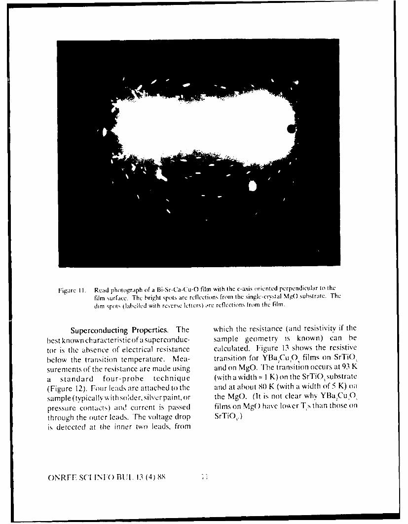
Figure 11. Read photograph of a Hi-Sr-Ca-C'u-C) film with the c-axis oriented perpendicular to the
film surface. The bright spots arc reflections, from the singic-crystal Nig() substraic. The
dim spo , (iabeI~cd with reverse letters,) e.rc reflections from the film.
Superconducting Properties. The which the resistance (and resistivity if the
best knowkn ch.aracteristic of a superconduic- sample geometry is known) can he
tor is the absence of electrical resistance calculated. Figure 13 shows, the resistive
below the transition temperature. Mea- transition for YI3a 2Cu, 9 films on SrTiO,
surements of the resistance are Made using and on MgO. TVhe transition occurs at 93 K
a standard four-probe technique (with awidth = K) on the SrTiO, substrate
(Figure 12). Four leads are attached to the and at about 80 K (with a width of 5 K) o;1
sample (typically" ith so~der, silvcrpaiflt, or the MgO. (it is not clear why~ YBaCuO,
pressure contacts,) Wnd current is passed films on MgO have low~er Tcs than those on
through the outer leads. The voltage drop SrTiO,.)is detected at the inner two leads, from
ONREE SCI INTO BUIL 13 (4) 88

With this technique one can estab-lish an upper bound on the resistance, but ofcourse one cannot ascertain that the resis-tance is actually zero. Plots of resistivityversus temperature only show where theresistivity falls below the limit of detect-
V. V ability (typically 10- ° ohm-cm). By "R =0"we mean the resistance is below instrumen-tal sensitivity. More sophisticated tech-
Figure 12. Four-probc resistance configuration. niques (Ref 8) have shown that the resistiv-ity of the "123" material is less than108" ohm-cm at 77 K.
0.8
MgO Substrate900 °C anneal
0.6
0.4
0.2SrTiO substrate850 °C anneal
0.00 50 100 150 200 250 300
Temperature (K)
Figure 13. Resistivity versus temperature curves for films of YBa2Cu O, on MgO and SrTi(). The filmof SrTiO, is pictured in Figures 5 and 6.
ONRFE SCI INFO BUL 13 (4) 88 12

Superconductors exclude magnetic temperature and field strength (exceptflux (the Meissner effect), but sufficiently close to T.). Figures 14 and 15 show plots oflarge magnetic fields destroy superconduc- J. as a function of temperature and of fieldtivity (Ref 9). There are two kinds of super- for the highly oriented "123" film describedconductors: type I and type II. In ideal above.type I superconductors there is a criticalmagnetic field, H., below which all flux is 10
expelled (from a thin rod parallel to thefield) and above which the superconductiv- 106
ity is destroyed. The high Tc materials are 105
type ii superconductors. In these supercon-ductors there are lower and upper critical .
magnetic fields, H, and H C. Fields whose < 10"
strength is below lI, are totally excluded, --
just as in type I superconductors. In fields 103larger than H c, but smaller than t11, the 0
system is in the mixed state, in which flux 102penetrates in the form of a lattice of normal B - 0(nonsuperconductor) cores surrounded by 101 .0 4 60 . 1
vortices of supercurrent. At H. flux pene- 0 20 40 60 80 100
trates the entire sample, which is then T [K]completely normal. In these new materials Figure 14. Critical current density versusHc at 4 K is typically 300 to 500 gauss (G) temperature at ambient (Earth)
and H, is 10' to 10 G. magnetic field for the film pictured inThe self fields generated by large Figures 5 and6.
currents drive superconductors into themixed state, with the cores (and therefore 107 •
the fluxoids) pinned to material imperfec-tions. The transport current exerts Lorentz 106forces on the cores, which remain immobile T=4.2K
as long as the pinning forces are not - OOO**ooexceeded. When the pinning forces are e 105overcome by the Lorentz forces, the coresmove. Irreversible work is then done by the 104
transport current and energy is dissipated;i.e., there is finite resistance in the super-conductor. The current density atwhich this i3 T=77Koccurs is called the critical current Jensity,J. This is an important quantity for thosetechnological applications where films 0 20 40 60 80 100
must carry large currents. A good film has H (kOeIa J of 10 A/cml at 4K in zero magnetic field Figure 15. Critical current density versusand is relatively insensitive to increasing magnetic field strength for the film
pictured in Figures 5 and 6.
ONRFE SCI INFO BUL 13 (4) 88 13

The Importance of Thin Films (Ref 11), as well as new hybrid devicesoperating at 77 K offer a new generation of
Oriented or single crystal thin films technology while avoidingthe difficulties ofprovide a means to study the anisotropic operating at very low temperatures.nature of the high temperature supercon- The Japanese are mounting a sub-ductors. As Figure 2 shos, the unit cell of stantial effort to develop high T thin filmthe "123" material has c/a =-3. The newer technologywith a strong emphasis on appli-bismuth- and thallium-based superconduc- cations. We report now on visits to severaltors have ratios from 4.5 to 9, with corre- laboratories.sponding T s from 20 to 125 K. Electricaland magnetic properties are different in the JAPANESE LABORATORIESa and c directions and possibly in the a andb directions. Electrical transport (i.e., resis- Kyoto Universitytivity and critical current), magnetic suscep-tibility, x-ray, and optical (i.e., reflectance The group at the Institute forand absorption) measurements are tools Chemical Research, led by Professorthat are sensitive to the anisotropy. Film Y. Bando, is growing single crystal films ofgrowth also allows the possibility of mul- YBaCu O on (100) and (110) SrTiO3 bytiple layering to produce tunnel junctions activated reactive evaporation, that is, in anand proximity effect systems. Such geome- oxygen plasma (Ref 12). The films aretries will allow the study of anisotropic grown by coevaporation from three metaltunnel junctions and proximity effect sources onto 500- to 650-'C substrates atdevices consisting of layers of high T super- rates of 4 to 6 A/s. The films are depositedconductors with normal metals, semicon- with the a-b plane parallel to the surface onductors, or other superconductors (Ref 9: the (100) substrate and with the (110) orSchuller, Tachiki, and Callen). (103) planes parallel to the surface on the
Technologically, thin films are the (110) substrate. RHEED studies show themajor avenue through which superconduc- films to be single crystals.tors can be coupled with semiconductors. Following a postanneal at 500'C forThe high temperatures needed to form 1 hour in oxygen, the resistance of the filmssuperconducting filins degrade the in the a-b plane orientation becomes negli-semiconductor-high T superconductor sys- gible a: 90.2 K with a width of 1.7 K. A filmtem, so it is clear that hybrid electronic as thin as 100 A showed a transition at 82 K.applicationswill require lower temperature The J of a 1,000-A film at 77 K was aprocessing schedules. Once this problem is respectable 4 x 10" A/cm2 . This work isovercome, the ability to interface the two significant because it shows that epitaxialtechnologies in the temperature range films with high critical currents can bewhere both are capable of high perfor- grown without the high temperaturemance will lead to powerful devices. Tradi- anneals (800 'C) commonly used in othertional superconducting devices such as laboratories.superconductor-normal-superconductor Contact: Prof. Yoshichika Bando;(SNS) mixers (Ref 10), superconducting Institute for Chemical Research, Kyotoquantum interference devices (SQUIDS) University, Uji, Kyoto-fu 611, Japan.
ONRFE SCI INFO BUI. 13 (4) 88 14

Nippon Telephone and Telegraph (NIT) YBa2Cu30.. Films of "123" areElectrical Communications Laboratory, evaporated from metals in K-cells in thelbaraki presence of ionic oxygen onto (100) and
(110) SrTiO 3 at 700 'C. The Bell LabsThe NTT Ibaraki group is mounting method (Ref 13) of replacing barium metal
a substantial effort in the growth of "123" with barium fluoride is used to better con-bismuth-based films as well as films of the trol the barium concentration. So far,original "214" 40-K superconductor. attempts at epitaxial growth with no post-
anneal are off stoichiometry and have someLa,.SrCuO. Single-crystal "214" bad spots. The transitions are broad with
films (x=0.1) are epitaxially grown with a negligible resistance at 82 K. This may besingle-target, rf magnetron sputtering sys- due to fluorine left in the film from thetem depositing at 120 A/min onto SrTiO, barium fluoride. Films on the (110) sub-(100) and (110) substrates at 800 'C. After strate have rough surfaces while those ondeposition the films are annealed at 800C the (001) substrate are smooth. This char-for8 hours inair. The filmsgrowin the (001) acteristic is important since surfaces mustorientation on the (100) substrate and in the be smooth for device applications.(103) orientation on the (110) substrate. Films are also deposited in situ with
These films are patterned with rf magnetron sputtering from a single targetdilute acid for Hall effect and resistivity (adjusting the Cu concentration with pelletsmeasurements. Deconvolution of the or a second Cu target) onto 600-'C SrTiO3measurements on films of several different and sapphire substrates. A most impressiveorientations shows that the resistivity is result is a 3,000-A-thick, c-axis-orientedabout the same in the a and b directions. At EuBaCu,O, film deposited at 650 'C onto300 K the resistivity in the c direction is sapphire. With no postanneal this film hasabout 20 times less than in the a and negligible resistance at 80 K. This is anb directions and at 40 K about 30 times less. important result for applications since sap-The upper critical field, HC, with the field phire has better dielectric properties thanparallel to the c-axis, is 5.2 times that per- SrTiO 3 and again shows that high tempera-pendicular. The Hall coefficient, R,, which ture postanneals are not necessary.is proportional to the inverse of the numberof carriers, is positive in all directions, indi- Bismuth Superconductor. Films ofcating the dominance of hole carriers. (This the bismuth-based superconductor arecontrasts with the "123" materials, which sputtered onto MgO at 580 C in aare holelike in the a-b plane and electron- 50-percent oxygen/argon plasma from alike in the c direction.) The Hall coefficient BiSrCaCu,O x target. As-grown films havein the a-b plane is four times that in the "zero resistance" at 56 K, and after anc direction. Superconducting transitions 880-C postanneal, at 90 K. X-ray diffrac-are broad, with resistivity onsets at around tion shows the presence of the 85-K phase40 K and negligible resistance only below 15 with c = 30 A and of the 110-K phase withto 18 K, depending on the sample. c = 36 A.
ONRFE SCI INFO BUL 13 (4) 88 15

Exploratory Devices. Simple tech- "R = 0" below 70 K. A postanneal at 880 'Cniques for making junctions are being for one-half hour in ionic oxygen followedexplored. The NTT group has grown a by a slow cool raises the "R=0" tempera-multilayer system consisting of a 3,000-A ture to 100 to 103 K. SEM observation afterEuBa2Cu 0 layer, 30-A Al 203 barrier layer, the high temperature deposition revealsand 1,000-A (110) niobium layer. X-ray what appears to be a film solidified from aanalysis shows the system to be epitaxial. melt. Fukutomi proposes that the filmsResistance measurements show aT of 75 K, grow from a molten layer. The films are notbut as of June 1988 junctions still had pin- uniform over the entire area of the sub-hole and surface roughness problems. A strate. X-ray analysis shows the major5x2 micron microbridge was patterned by component to be the 85-K phase withargon milling to make a SQUID. The c = 30 A. The films are highly oriented withdevice has aJ of about4x 10'A/cm2at4.2 K the c-axis perpendicular to the surface.and shows granular behavior including X-ray analysis also indicates the presence ofrf-induced voltage steps in the I-V curve the high temperature phase with c = 37 A.typical of Josephson junctions. Contacts: M. Fukutomi, Hiroshi
Contacts: Y. Enomoto, Maeda, H. Sekine, T. Takeuchi, Yoshiaki0. Michikami, T. Murakami, M. Suzuki; Tanaka, H. Wada; National Research Insti-Nippon Telephone and Telegraph Electri- tute for Metals, 1-2-1 Sengen. Tstikuba-shi,cal Communications Laboratory, Tokai, Ibaraki-ken 305, Japan.Ibaraki 319-11, Japan.
Electrotechnical Laboratory (ETL),National Research Institute for Metals Tsukuba(NRIM), Tsukuba Laboratories
A joint government-industry-This iaboratory is well known for university group is sputtering Y-based
developing superconducting magnet wires "123" from stoichiometric targets (Ref 16).of conventional superconductors (Ref 14), They deposit 3,000- to 8,000-A films onand H. Sekine and coworkers are now (100)MgOandSiTiO 3 at500to650'Cusingdeveloping wires of the high Tc supercon- a conventional rf diode system with a 1:1ductors. The group is also well known for argon:oxygen atmosphere. A commonthe discovery by Maeda et al. of the bulk problem with the sputtering technique isBi-Sr-Ca-Cu-O superconductor (Ref 15). that the stoichiometry of the deposited filmM. Fukutomi is leading the effort to deposit usually differs from that of the target. Thefilms of this material. Films are rf mag- ETL group solves this problem by isolatingnetron sputtered from a single sintered the substrate from the flux of negative ionstarget of Bi,1 SrCaCuO in 3 x 10² Torr of and secondary electrons. They believe thatargon onto (100) MgO. Substrate temper- ion bombardment weakens the Ba-0 andature is carefully controlled while sputter- Cu-0 bonds of the growing film, resulting ining: 800'C for the first 10to 15 minutes and the deficiencies in barium and copperthen at between 700 and 740 'C for the rest observed in films that are not isolated fromof the deposition. The as-grown films have the ion flux. The stoichiometry of films
;1Zl i '( 1 I', I( k t ;I -) , 16

grown in the isolated configuration, as The important conclusion is that themeasured with EPMA (electron- substrate must be above 600 'C duriricmicroprobe) and other methods, matches deposition to achieve epitaxial growQi.that of the "123" target for a wide range ofchamber pressures and substrate tempera-tures. The best fili are grown at 580'C and 900 -
low pressure (less than 10 mTorr) to reducesurface roughness. The films have (100)orientation as grown, less than 20-,A surface __
features (as determined by SEM and acommercial stvlus instrument), and resis- 7--tive onsets around 85 K, with "R = 0" a little " It,...above 80 K.
Contacts: 1l. hara, K. Murata,N. Terada, M. Tokumoto; Electrotechnical Amorphous
Laboratory, 1-1-4 Umezono, Sakura, IcNiihari, lbaraki-ken 305, Japan.
Sumitomo Electric Industries, Itami City 400
This group, led by Dr. Hi. Itozaki, -
makes rf-sputtered films of REBa 2Cu.3O 0 40 SM 600 oo
with RE=Y, La, Nd, Sm, Eu, Gd, Dy, Ho, Subst'rate Temp. Ts (C)Er, and Yb on (001) MgO (Ref 17). Thesubstrates are at 400 to 800 °C, the atmo-sphere is 80 percent argon/20 percent oxy- Figure 16. Summary of the results of Sumimianncaling studics for the cpitaxialgen, and the target stoichiometries are growth of HoBa2Cu.O7 (from Rcf 17).1:2.2:3.4 (RE:Ba:Cu). Their 7,000-A films The substrate must be hotter thangrow at about 20 to 50 A/min. By carefully 000 'C during the deposition to obtain
adjusting the sputtering conditions the cpi!axial growth.
Sumitomo group can deposit RE= Er, Y,Ho, and Dy films onto 750-°C substrates. Their best Ho films are epitaxiallyThe films are metallic, oriented with their grown tinder the conditions describedc-axes perpendicular to the surface, and above, followed by a 920-'C anneal in flow-have T s above 80 K. Gd, Eu, and Sm films ing oxygen. X-ray studies confirm thedeposited on substrates at temperatures single-crystal nature of the films and SEMexceeding790°Calso have these properties. observations show less than 50-A surface
Epitaxial growth of the Ho "123" roughness. The resistive transition is atsystem has been carefully studied 84 Kand is0.4 Kwide. The critical current(Ref 17,18). Figure 16 summarizes the density,J,at77Kis3.53x 106A/cm inzcroresults of the substrate heating and applied magnetic field and 1.5 x 10⁶ A/cm'postanneal studies by the Sumitomo group. in a 1.0-tesla field parallel to the c-axis.
ONRFE SCI INFO BUL 13 (4) 88 17

These remarkable critical currents were They are tackling difficult materials proh-measured byan ac method (Ref 18). Recent lems while laying the essential groundworkac susceptibility measurements by for fabricating devices of these new mate-Malozemoff et al. (Ref 19) show that the rials.behavior of fluxoids in these materials is A major thrust of their research is tosensitive to frequency. A magnetic field develop the technology that will be neededenhances this sensitivity. Since the critical for device applications. With this objectivecurrent is limited by motion of fluxoids in in mind they are studying the properties ofthe superconductor, measurements made etchants (Ref 25,26) on polycrystallineat ' finite frequency in a magnetic field can "123" films. Their initial results show thatgive anomalous results. 2-micron features can be patterned with
Finally, Sumitomo showed us some phosphoric acid without affecting Tpreliminary work on other projects. Sput- (Ref 26).tered films of Y-Ba-Cu-O on MgO have an In any application the superconduct-extraordinary J at 77 K of 1.2 x 10 'A/cm 2 in ing element, film or bulk, must be coupledan 8-tesla magnetic field. They are sputter- to normal or semiconducting componentsing films onto Al 203 that have negligible or leads. High-resistance interfaces intro-resistance at 81 K but have low Js. ducelocalheatingandnoise,whichdegradeSumitomo is fabricating Josephson junc- device performance. To address this prob-tions and SQUIDS that operate at 4.2 K. lem the Kobayashi group is exploring theSumitomo is also working on the new use of silver, tin-oxide, and indium-tin-thallium- and bismuth-based superconduc- oxide to make low resistance contacts totors. Their preliminary work (as of films.September 1988) has produced TI-Ba-Ca- They are also studying the charac-Cu-O films with "R=O" at 124 K and terization of films by electron spectroscopyJo = 3.2x 10" A/cm at 80 K in zero field but for chemical analysis (ESCA) (Ref 27,28).which falls off sharply with field. The In ESCA [which is also called x-ray photo-Bi-Sr-Ca-Cu-O films have "mirror-quality" emission spectroscopy (XPS)], the film issurfaces, "R=0" at 106 K, and J = exposed to x rays and the energies of the1.7 x 106 A/cm 2 at 77 K in zero field. There emitted secondary electrons, characteristicis some significant dropoff of Jc with field of the elements, are measured. A depthbut not so severe as with the TI films. profile is constructed by making measure-
Contact: K. Higaki, H. Itozaki, ments as the film is milled by an argon ionS. Tanaka; Sumitomo Electric Industries beam.Ltd., Itami R&D Laboratory, 1-1, 1-chome Oxygen plasma is an efficient way toKoyakita, Itami, Hyogo 663, Japan. oxidize these superconductors. Prof.
Kobayashi and his students have madeOsaka University detailed studies of the electron cyclotron
resonance (ECR) microwave plasma oxida-Professor T. Kobayashi and his tion process in "123" films (Ref 29). ECR
students are building on their experience ionizes oxygen at low pressures with mini-in conventional superconductor- mal heating of the plasma. This allowssemiconductor devices (Ref 20-24) to better control of the plasma during process-develop devices with high T, materials. ing.
ONRFE SCI INFO BUL 13 (4) 88 18

The Kobavashi group's most excit- Y BaCuOing activity is the epitaxial growth of a ErBaCuOmultiple heterostructure with "123" layers L-.YBoCuO(Ref 30,31). Films are deposited with an rf 60nm 1 &r~oCu
magnetron system from off-stoichiometric (110) SrTiO3 |" Y Bo u0
targets onto (110) SrTi), at 670 'C in an L Jargon+40 percent oxygen plasma. FirstKobavashi demonstrated that 1,200 A of Figure 17. Multiple hetcrostructure consisting of
either Er "123" or Nd " 123" will grow epi- YBa,Cu 07 and ErBalCu3 0. 0a-yerstaxially on epitaxial Y -123." RItEED (AX Athick on (110) SrTiO, [frommeasurements sho\w the films have (110) Superconductivit', vol 6, Proceedingsorientation, but there is some slight of the MRS International Meeting on
Advanced Materials, Tokyo, Maydegradation of the crystal quality, especially 198 Tobe published in 1989. Used
with Er. Kobayashi and his energetic stu- with permission of the Materialsdents are now growing multiple hetero- Research Society (Rcf .0)1.
structures (Figure 17) consisting of alter-nate Y "123" and Er "123" layers, each Matsushita Electric Industrial Co., Ltd.,600 A thick. Epitaxy is retained'in succes- Osakasive layers but with some deterioration ofcrystal quality. The Kobayashi group has This powerful group, led by Dr.also grown 100-, 30-, and 12-A epitaxial K. Wasa, using rf magnetron sputtering, hasfilms of Y "123" on (110) and (100) SrTiO, grown films of each of the high temperatureand on (100) MgO. Crystailine distortion is superconductors (Ref 32-37). We willevident in the accommodation of the 12- report only on some of the highlights of theirand 30-A films to the SrTiO, substrate but recent work. They have studied the proper-not for the 100-A film nor for films of any ties of ErBa2CuO films on sapphire as athickness on MgO. Heterostructures of function of film thickness (Ref 33). Thealternate 12-A-thick lavers of Er "123" and films were grown on R-plane sapphire atY "123" have been grown ona(l10) SrTiO, 650 'C from a 1:2:4.5 target at a rate ofbase. RHEED analysis shows some distor- 40A/s in a 1:1 Ar/O plasma. Thin filmstion of the crystal. As of June 1988, no (0.15 and 0.3 micron thick) have semicon-transport measurements had been made ductorlike resistance behavior with super-and the superconducting properties were conducting onsets at 91 K and very broadunknown. transitions. The films improved with
Contact: Takeshi Kobayashi; increasing thickness, eventually showingFaculty of Engineering Science, Osaka metallic behavior and sharper transitions.University, 1-I Machikaneyama, A 1-micron film had negligible resistance atToyonaka, Osaka 560, Japan. 80 K and Jc of 2 x 10 A/cm2 at 4.2 K.
Migration of atoms of the sapphire sub-strate into the film is responsible for thepoor behavior of the thinner films.
ONRFE. SCI INFO BUL 13 (4) 88 19

The Matsushita group is sputtering superconducting onset above 115 K andfilms of the bismuth superconductor "R=0" at 102 K. The highest Jc in ambient(Ref 34-36) from a Bi _SrCa .Cu O target magnetic field is 8.5 x 1O A/cm-at 4.2 K andin a plasma with argon,/oxygen ratios of 1.2 x 10 A/cm' at 77 K for a film annealedfrom 1:1 to 1:1.5. The best films are grown at 890 'C. It is clear that these films areon (100) MgO substrates at 800 'C, post- extremelysensitive toannealingand furtherannealed in flowing oxygen at 900 'C for work is in progress.20 minutes, and then held at 865 'C for Contact: Kentaro Setsune, Kiyotaka5 hours. X-rav diffraction shows only broad Wasa; Matsushita Electric Industrial Co..peaks corresponding to the 120-K phase Ltd., Central Research Laboratories,with c = 36 A, oriented perpendicular to the Moriguchi, Osaka 570, Japan.surface. Resistance measurements showthe superconducting onset at 115 K and CONCLUDING REMARKS-R=0- at 1(4 K. Initial critical currentmeasurements yield J =I(Y A/cm at 90 K This completes our report on ourin the ambient (Earth) magnetic field, laboratory visits. The body of work done by
Wasa and coworkers are also sput- these laboratories and by the many othertering films of the thallium superconductor Japanese high T laboratories is impressive.from a Il BtaCaCu, 0 target in a plasnla especially considering that the field is lesswith argon/oxygen = 1I onto ( 100) MgO than 2 years old. Many advances have beensubstrates (Rcf 31,37). The substrates are made in laying the foundations of a futureonly warmed to 20() -C by the plasma since superconducting technology.heating them aboe 400 'C causes the thai- At frequent symposia Japaneselium to reevaporate from the films. These industrial, university, and national labora-conditions produce films with the composi- tory groups share information on their owntion TI,Ba CaCuO. Since thallium has a progress and report on world-wide develop-high vapor pressure at relatively low tem- ments. Interlaboratory work groups attackperatures, the tilrns are put in a cloised common problems. Japan is building on itsalumimi crucible ard postannealed in flow- strength in conventional superconductivity.Ing oxygen and thallium vapor at 900 'C for With the advent of high T, the "low [1 minute. The postannealed films' compo- budget has been increased. Researchsition is TI BaCaCu, (). X-ray diffrac- groups are enthusiastic, are well equipped.tion shows sharp peaks correp ,)nding tothe and are strongly backed by management"2212" (lowerr) phae with c = 30 A and and the Japanese Government. Forhighly oriented perpendicular to the sir- example, Hitachi, which we did not reportface. %latushita researchers also obtain on here, spends 10 percent of its sales onthe higtler T phase wkith c = 36 A. but it is research and development (R&D) aridunstable. Resistance rmeasurenmnts of the product develOpment.* In the course of-best film, an nealed at 9(0()'. have the attacking the many difficult problems that
*lotal I litachi sale,, in 1987 %k cre S22.5 bill ion and R&[)expeuditures totalled S2 billion. Netincome \kas S5() million.
ONRFI" SCI INFO B'I., 13 (4) 88 20

must be solved, Japanese researchers are 5. B.D. Cullity, Elements of X-Rayo Dif-gaining the "know how" that is going to fraction (Addison-Wesley, 1978);stand them in good stead in getting to the M.M. Woolfson, An Introduction to X-Raymarket with high T, devices. Crystallography (Cambridge University
Press, 1970).
ACKNOWLEDGMENT6. M.G. Lagally, Methods of Experi-
The authors wish to thank mental Physics 22 (Academic Press, Inc.),E.F. Skelton for providing x-ray data, p. 237.H.A. Hoff for microscopy data, andL.H. Allen for critical current density data. 7. M. Prutton, Vacuum 22, 1563 (1972).They also wish to thank E.F. Skelton,H.A. Hoff, and R.J. Soulen, Jr., for their 8. E.M. Gyorgy, G.S. Grader,useful comments on the manuscript. The D.W. Johnson, Jr., L.C. Feldman,authors acknowledge the support of the D.W. Murphy, W.W. Rhodes.Office of Naval Research (ONR); the R.E. Howard, P.M. Mankiewich, andOffice of Naval Technology (ONT); the W.J. Skocpol, Appl. Phys. Lett. 52. 328Strategic Defense Initiative, Office of Inno- (1Q88).vative Science and Technology (SDIO/IST); the Defense Advanced Research 9. A.C. Rose-Innes and E.H. Rhodrick,Project Agency (DARPA); and the Nuclear "Introduction to superconductivity," Inter-Defense Agency (NDA). national Series in Solid State Physics,
Volume 6 (Pergamon, 1978); G.B. Wright,
REFERENCES "A short tutorial on superconductivity,"ONRFE Scientific Information Bulletin
1. P.R. Broussard and S.A. Wolf, to be 13(1), 24-36 (1988); I.K. Schuller,published in J. Crystal Growth. M. Tachiki, and E. Callen, "Dimensional
crossover in superconducting superlat-2. M. Leung, P.R. Broussard, tices," ONRFE Scientific InformationJ.H. Claassen, M. Osofsky, and S.A. Wolf, Bulletin 13(3), 1-21 (1988).AppI. Phys. Lett. 51, 2046 (1987).
10. B.B. Schwartz and S. Foner. "Super-
3. I-.A. Hoff, A.K. Singh, J.S. Wallace, conductor applications: SQUIDS andW.L. Lechter, and C.S. Pande, J. machines," Nato Advanced Study lnstitutesSuperconductivity 1,35 (1988). Series, Series B: Physics. Volume 21
(Plenum Press, 1977).4. W.P. Lowe, Ph.D. thesis, StanfordUniversity, W.W. Hanson Laboratories of 11. T. Van Duzer and C.W. Turner, Prin-Physics, 1983, p. 12. ciples of Superconductie Devices and Cir-
cuits (Elsevier North lolland, Inc., 1981).
ONRIFE SCI INFO BL;I, 13 (4) 88 21

12. Y. Bando, T. Terashima, and 21. M. Tonouchi, H. Sakai, andH. Mazaki, Superconductivity, vol 6, T. Kobayashi, Jpn. J. Appl. Phys. 25, 705Proceedings of the MRS International (1986).Meeting on Advanced Materials, Tokyo,May 1988 (to be published in 1989). 22. H. Sakai, Y. Kurita, M.Tonouchi, and
T. Kobayashi, Jpn. J. Appl. Phys. 25, 83513. P.M. Mankiewich, J.H. Scofield, (1986).W.J. Skocpol, R.E. Howard, A.H. Dayem,and E. Good, Appl. Phys. Lett. 51, 1753 23. M. Tonouchi, H. Sakai, and(1987). T. Kobayashi, J. Appl. Phys. 62, 961 (1987).
14. T. Takeuchi, Y. Iijima, and K. Inoue, 24. M. Tonouchi, K. Hashimoto,Superconductivity, vol 6, Proceedings of the Y. Sakaguchi, S. Kita, and T. Kobayashi,MRS International Meeting on Advanced ExtendedAbstracts ofthe 19th Conference onMaterials, Tokyo, May 1988 (to be Solid State Devices and Materials, Tokyopublished in 1989). (1987), p. 171.
15. M. Maeda, Y. Tanaka, M. Fukutomi, 25. M. Tonouchi, Y. Sakaguchi, S. Kita,and T. Asano, Jpn. J. Appl. Phys. (in press). and T. Kobayashi, Jpn. J. Appl. Phys. 27,
L98 (1988).16. N. Terada, H. Ihara, M. Jo,M. Hirabayashi, Y. Kimura, K. Matsutani, 26. Y. Yoshizako, M. Tonouchi, andK. Hirata, E. Ohno, R. Sugise, and T. Kobayashi, Jpn. J. Appl. Phys. 26, L1533F. Kawashima, Jpn. J. Appl. Phys. 27, L639 (1987).(1988).
27. M. Tonouchi and T. Kobayashi,17. H. Itozaki, S. Tanaka, K. Harada, Superconductivity, vol 6, Proceedings of theK. Higaki, N. Fujimori, and S. Yazu, Pro- MRS International Meeting on Advancedceedings of the Fifth International Workshop Materials, Tokyo, May 1988 (to beon Future Electron Devices-High Tempera- published in 1989).ture Superconducting Devices, Zao, Japan,2-4 June 1988. 28. M. Tonouchi, Y. Yoshizako,
T. Takahashi, Y. Sakaguchi, S. Kita,18. S. Tanaka and H. Itozaki, Jpn.J. Appi. Y. Fujiwara, and T. Kobayashi,Jpn. J. Appl.Phys. 27, L622 (1988). Phys. 26, L1462 (1978).
19. A.P. Malozemoff, T.K. Worthington, 29. S. Minomo, M. Taniguchi, Y. Ishida.Y. Yeshurun, and F. Holtzberg, to be pub- M. Sugiyo, T. Takahashi, M. Tonouchi,lished in Phys. Rev. B (1 September 1988). S. Kita, and T. Kobayashi, Jpn. J. Appl.
Phys. 27, L411 (1988).20. T. Kobayashi, H. Sakai, Y. Kurita,M. Tonouchi, and M. Okada, Jpn. J. Appl.Phys. 25, 402 (1986).
ONRFE SCI INFO BUL 13 (4) 88 22
30. M. Tonouchi, Y. Yoshizako, M. lyori, Michael S. Osofsky received a B.S. inand T. Kobayashi, Superconductivity, vol 6, physics in 1979from the Massachusetts Insti-Proceedings of the MRS International tute of Technology, and a M.S. and Ph.D. inMeeting on Advanced Materials, Tokyo, physics in 1981 and 1987 fron the UniversityMay 1988 (to be published in 1989). of Illinois, Urbana. From 1981 to 1986
Dr. Osofsky conducted research at the31. M. Tonouchi, Y. Yoshizako, M. Iyori, University of Illinois in amorphous materialsand T. Kobayashi, Proceedings of the Fifth near the metal-insulator transition. SinceInternational Workshop on Future Electron October 1986 lie has been working in highDevices-High Temperature Superconducting temperature superconductivi' at the NavalDevices, Zao, Japan, 2-4 June 1988. Research Laboratory. Dr. Osofskys technical
experience includes thin film vacuum32. H. Adachi, K. Setsune, and K. Wasa, evaporation, cryogenic techniques, x-rayPhys. Rev. B35, 8824 (1987). diffraction, design and construction of
electron optical components, and operation33. K. Hirochi, H. Adachi, K. Setsune. of VTS SQUID susceptonzeter. Within the0. Yamazaki, and K. Wasa, Jpn. J. Appl. past year or two he as written or coauthoredPhys. 26, L1837 (1987). more than a dozen publications on high T,
superconductors.34. H. Adachi, Y. Ichikawa, K. Setsune, Phillip R. Broussard graduatedS. Hatta, K. Hirochi, and K. Wasa, Jpn. J. Summa Cuinz Laude from Louisiana StateApp). Phys. 27, L643 (1988). University and received his Ph.D. in applied
physi-s at Stanford University under Prof.35. Y. Ichikawa, H. Adachi, K. Hirochi, T.H. Geballe. A NationalResearch CouncilK. Setsune, and K. Wasa, Superconductivity, postdoctoral fellow at the Naval Researchvol 6, Proceedings of the MRS International Laboratory, Dr. Broussard is the author ofMeeting on Advanced Materials, Tokyo, 10papers on sputtered niobium, zirconium.,May 1988 (to be published in 1989). and tantalum multilayers and on high T
films.36. K. Wasa, H. Adachi, Y. Ichikawa, Earl Callen is a menberof the staff ofK. Setsune, and K. Hirochi, Superconduc- the Office of Naval Research Far East. He istivity, vol 6, Proceedings of the MRS Inter- a Professor Emeritus of The American Uni-national Meeting on Advanced Materials, versity. He received his Ph.D. under JohnTokyo, May 1988 (to be published in 1989). Slater at MIT and has been active in the
physics of magnetoelastic phenomena and37. Y. Ichikawa, H. Adachi, K. Setsune, amorphousmagnetism. In thefirst cycle of hisS. Hatta, K. Hirochi, and K. Wasa, sub- life lie was much involved in physics andmitted to Appl. Phys. Lett. public affairs.
ONRFE SCI INFO BUL 13 (4) 88 23

RESEARCH INSTITUTE FOR METAL SURFACEOF HIGH PERFORMANCE (RIMES):An Example of Japanese Transferof Technology Techniques
Fred Pettit
R IMES is a research and development made to permit each company to use the(R&D) company that illustrates a new technology generated in ways most
strategy followed to establish new and effective for its own specific products.advanced technologies in Japanese indus- RIMES has 17 company memberstry. An R&D target having potential for (see memberhip li,,t of Jatpan Rescarch ardexploitation is identified by using the input Development ('enter for Metals). mainlyfrom industry, academia, and government, steel and nonferrous metal )roLlIcers.The targeted technology is developed or Each company is encouraged to prov'ideadvanced in certain companies through the researchers to work at RIMES. Moreover,formation of a transitory R&D venture RIMES is located at the facilities of one ofinvolving the direct participation of the participating companies. The buildingemployees from these companies. Govern- for RIMES is isolated from the rest of thismental leadership coupled with the enthu- company's facilities and the researcherssiastic participation of industry and aca- from the other companies do not have freedemia are important characteristics of this access to the host company's facilities othertechnology transfer process. than RIMES' building. Each month the
researchers at RIMES have discussions oftheir recent results with representatives of
RIMES is an acronym for Research theparticipating companies present. More-Institute for Metal Surface of High Perfor- over, the individual researchers have moremance. It is a special research and develop- frequent meetings with technical represen-ment (R&D) company composed of tatives from their parent company. WritteTresearchers from different companies with reports are prcparcd at prescribed timea common interest. That interest is coat- intervals and are available to the membersings, especially SiC coatings, deposited on of RIMES. Researchers are assigned tomaterials by using chemical vapor deposi- RIMES by their parent company for ation techniques. The companies in RIMES period of 2 years. At the end of that periodmay be competitors in regards to their prod- they may be appointed for another 2-yearucts, and they only share the technical data term or go back to their parent company.generated at RIMES. RIMES has been in One of the objectives of RIMES is toexistence for 2 years, and it will exist for a develop coatings expertise back in the indi-period of 6 years. After that time sup- vidual companies, so one researcher willposedly enough progress will have been usually not stay at RIMES for the full 6-year
period.
ONRFE SCI INFO BUL 13 (4) 88 25
Since RIMES is concerned with empirical. For example, the deposition ofadvancing and transferring the technology SiC coatings on alloys at elevated tempera-of chemical vapor deposition (CVD), three tures is affected by silicide and carbidetypes of CVD are being investigated: ther- formation in the alloys. The RIMESmal CVD, plasma-assisted CVD, and research examines the various possiblemetal-organic CVD. These techniques are reactions using thermodynamic considera-being used to form SiC coatings on various tionsto attempt todetermine the conditionsalloys. After 2 years of effort equipment has that will produce the most desirable coat-been installed and is now operational to ings. The researchers are young, conscien-deposit coatings by each of these tech- tious, and enthusiastic, with mastersniques. Each apparatus is in a separate degrees or the equivalent in experience.room in the RIMES building and is the They have been employed by their com-responsibility of a researcher from one of panies for at least about 5 years.the participating companies. RIMES has RIMES is an effective technologythe equipment to deposit coatings and advancement and transfer organization. Itmeasure coating thicknesses, but facilities permits companies to pool resources inare not available for in-depth characteriza- advancing technologies in which there is ation of the coatings by techniques such as common need. How was it formed? Howscanning electron microscopy or transmis- and why was the CVD deposition of SiCsion electron microscopy. Each researcher chosen as an important technology? How isattempts to characterize the coatings by it supported? To answer these questionsusing the facilities of his own company. If another organization must be considered--one company does not have a certain piece the Japan Research and Developmentof equipment to perform a required analysis Center for Metals (JRCM).or examination, but another company does, JRCM is a foundation in the Agencythe researcher from the company that has of Industrial Science and Technology,the equipment may perform the necessary which in turn is part of the Ministry ofwork. It is unusual for the other researcher International Trade and Industry (MITI).toaccompanyhim. In fact, such interactions JRCM was established in October 1985. Itswhere researchers from one company function is to support technologicalexamine specimens prepared by advancement in the metals-related area byresearchers from another company seem to helping to overcome obstacles such as fore-be rather few. seeing industrial needs, increased risks in
The work performed at RIMES is commercialization of new materials, andconcerned with defining procedures to fab- inefficient technology transfer. Financialricate, reproducibly, coatings with specific support forJRCM comes from MITI as wellproperties. The mechanisms by which the as from its 58 supporting members, whichcoatings are formed receive less emphasis; are as follows:however, the approach is far from totally
ONRFE SCI INFO BUL 13 (4) 88 26

Nippon Steel Corp.* Sumitomo Metal Mining Co., Ltd.*NKK Corp.* Nippon Light Metal Co., Ltd.Kawasaki Steel Corp.* Sumitomo Light Metal Industries, Ltd.Sumitomo Metal Industries, Ltd.* Showa Aluminum Corp.Kobe Steel, Ltd.* Mitsubishi Aluminum Co., Ltd.Nisshin Steel Co., Ltd.* Sky Aluminum Co., Ltd.Nakayama Steel Works, Ltd. The Furukawa Electric Co., Ltd.*Godo Steel, Ltd. Sumitomo Electric Industries, Ltd.Aichi Steel Works, Ltd. Fujikura Ltd.*Sanyo Special Steel Co., Ltd. Hitachi Cable, Ltd.*Daido Steel Co., Ltd.* Showa Electric Wire & Cable Co., Ltd.Topy Industries, Ltd. Mitsubishi Cable Industries, Ltd.Nippon Koshuha Steel Co., Ltd. Vacuum Metallurgical Co., Ltd.Hitachi Metals, Ltd. The Industrial Bank of Japan, Ltd.The Japan Steel Works, Ltd.* The Dai-ichi Kangyo Bank, Ltd.Mitsubishi Steel Manufacturing Co., Ltd. The Fuji Bank, Ltd.Nippon Metal Industry Co., Ltd. The Sanwa Bank, Ltd.Nippon Stainless Steel Co., Ltd. The Sumitomo Bank, Ltd.Nippon Yakin Kogyo Co., Ltd.* The Taiyo Kobe Bank, Ltd.Kanto Special Steel Works, Ltd.* Ishikawajima-Harima Heavy Industries Co., Ltd.*Kubota, Ltd. Toshiba Corp.Pacific Metals Co., Ltd. NEC Corp.Yodogawa Steel Works, Ltd. Hitachi, Ltd.Showa Denko K.K. Mitsubishi Heavy Industries, Ltd.Japan Metals & Chemicals Co., Ltd. Nissan Motor Co., Ltd.Nippon Denko Co., Ltd. Toyota Motor Corp.Nippon Mining Co., Ltd.* Kawasaki Heavy Industries, Ltd.Mitsubishi Metal Corp.* Mitsubishi Electric Corp.Mitsui Mining & Smelting Co., Ltd. Nippon Telegraph and Telephone Corp.
JRCM attempts to perform its func- materials, superconductivity, biotech-tion by emphasizing three "I"s: nology, aerospace, and ultrafine particles.
Experts from government, universities, and* Integration of User Needs and Maker industry are often invited to present lec-
Seeds tures and to help initiate discussions onspecific topics. The object is to obtain a
* Identification of R&D Targets variety of views on different subjects byproviding different forums for expression
* Implementation of Efficient R&D and interaction.The second "I," Identification of
The first "," Integration of User R&D Targets, ii the responsibility ofNeeds and Maker Seeds, involves the free JRCM's Research Committee, whoseexchange of information and opinions members include employees of JRCM,between metals producers and users. This university faculty, and employees of theis accomplished by a variety of techniques member companies. This committee isthat include salons or conversation rooms to constantly seeking to define new search anddiscuss specific topics such as electronic survey themes as they become evident
*Also a member of RIMES.
ONRFE SCI INFO BUL 13 (4) 88 27
through the "integration of user needs and reliability of light water reactor facilities aremaker seeds" process. The purpose of the examples of R&D projects currently beingsearch and survey is to examine in detail pursued byJRCM. Some typical feasibilitycertain topics to determine whether an studies have been concerned with:important R&D target can be identified. (1) aluminum-lithium alloys for aerospacePriority is given to the following: applications, (2) rapidly solidified alumi-
num plate, and (3) semisolid forming pro-. Projects that are difficult for a single cesses.
company to undertake independently. When appropriate the results fromthe R&D projects or the feasibility studies
* Projects ranging overwide areas of tech- are used to establish joint ventures betweennology. companies with mutual interests in the new
technology. While the development of such* Projects that require highly specialized joint ventures is the primary objective of
scientific and technological knowledge. JRCM, it is not directly involved with thenew venture. An R&D company is formed
* Projects that are high risk. composed of the participating companies.The capital for this R&D company is pro-
" Projects in which the available tech- vided by the participating companies and, ifnology is insufficient and a combined necessary, upto 70 percent of the capitaliza-effort on the part of metals users and tion can be obtained from the Japan Keyproducers is c sential. Technology Center (Japan Key-TEC),
whose function is to promote private sectorSearches and surveys were begun in 1988 to research and development of fundamentaldetermine the state-of-the-art and science technologies seen as providing an impor-of. (1) properties of materials and material tant impetus of progress toward the 21stprocessing technologies under extreme century society. Japan Key-TEC is part ofconditions such as super-high vacuum, the Ministry of International Trade andsuper-high pressure, super-high magnetic Industries and the Ministry of Posts andfield strength, super-high temperature, Telecommunications. Since its inceptionsuper-low gravity, and super-high rate of JRCM has established two R&D com-forming; (2) intermetallic compounds; and panies. One is RHEOTECH (rheotech-(3) single crystals. nology), which is concerned with the devel-
The third "I," Implementation, opment of the semisolid forming process foroccurs once the target has been set by the metallic materials. The other is RIMES. InResearch Committee. It can consist of an the September 13, 1988 issue of the JapanR&D projector a feasibility study. Ineither Industrial Journal it was announced thatcase such efforts are usually supervised by a seven aluminum manufacturers were tosenior researcher and piloted by a technical form an R&D company, "Alithium," for thecommittee in JRCM. Tubular goods for development of aluminum-lithium alloysevere environments encountered in oil production technologies. This project willproduction, materials for molten carbonate include: (1) research on the properties,fuel cells, and new materials for improved alloy design technology, and secondary and
ONRFE SCI INFO BUL 13 (4) 88 28

tertiary processing conditions necessary for that it not only brings the players togethereconomical production of good high- but it expertly stimulates their interactionstrength alloys; (2) establishment of new and adroitly identifies the key targets. Themelting/casting technologies for the pro- university and industrial participants acceptduction of safe, high-quality alloys that the governmental role especially during theinclude development of methods for reduc- initial stages of this process. The participa-ing hydrogen gas absorption and develop- tion of government decreases as the R&Dment of refractory materials and coolants company is formed, with the industrialthat do not react with lithium; and (3) estab- participants becoming the dominant partic-lishment of a scrap recycling process for ipants.enhanced cost performance. It is apparentthat a third R&D company will form F.S. Pettit is a liaison scientist withbecause of JRCM's efforts. ONR Far East. Professor Pettit is on sabbati-
R&D company combined ventures calfrom the Materials Science and Engineer-evolving from a network of governmental ing Department at the University oforganizations designed to incorporate the Pittsburgh. Dr. Pettit's professional interestsknowledge and experience of industry and arein high-temperature ni aterialsand surfaceacademia are not the exception but the rule stability and the use ofcoatingsforprotection.in Japan. Government plays a key role in
ONRFE SCI INFO BUL 13 (4) 88 29

RESEARCH AND APPLICATIONS OFMETALLIC SUPERLATTICES, HIGH T€SUPERCONDUCTORS, X-RAY OPTICS,AND COMPACT SYNCHROTRONS
Charles M. Falco
T his article describes research on metal- MRS INTERNATIONAL MEETINGlic superlattices, high Tc superconduc- ON ADVANCED MATERIALS
tors, and x-ray optics and also reports on thedevelopment of compact synchrotrons for Backgroundgeneration of soft-x-rays. This informationwas obtained at the Materials Research This meeting consisted of 21 sym-Society International Meeting on Advanced posia; I attended the multilayer and super-Materials in Tokyo and from the Japan conductivity symposia. I presented one ofResearch and Development Center for the plenary lectures in the multilayer sym-Metals (JRCM), Canon's Central Research posium, on metallic superlattices, andLaboratory, NEC Corporation, the Materials chaired the session on superconductivityScience Department at the University of and transport phenomena. Because of theTokyo, and Sumitomo Heavy Industries, concurrent symposium on superconductiv-
ity that was mostly high T., the superconduc-tivity work reported in the multilayer sym-
INTRODUCTION posium was mostly low To.
During a visit to Japan in May/June Multilayer Symposium1988 to speak at the Materials ResearchSociety (MRS) International Meeting on The organizers of the multilayerAdvanced Materials, I visited several labo- symposium told me they had contactedratories conducting research on metallic every Japanese group working on metallicsuperlattices, high Tc superconductors, and superlattices and that almost all of them hadx-ray optics and one company that is devel- contributed papers. The multilayer sym-oping a "compact" synchrotron, with a posium was the largest at the conference,number of scientific and technological running for four and a half days. Thus, thisapplications. This article describes infor- meeting was a good opportunity to gaugemation obtained during these visits, the extent of Japanese involvement in
ONRFE SCI INFO BUL 13 (4) 88 31
metallic superlattices. Japanese involve- Superconductivity Symposiumment is surprisingly large and doesn't seemto have "suffered" people moving out of it The general atmosphere at thisinto high Tc superconductivity, as has been symposium was strikingly low key, as corn-the case in the United States. pared to comparable sessions held at the
Judging from the addresses on the MRS meeting in Boston 6 months earlierabstracts for this symposium, there are and the American Physical Society meetingabout 23 Japanese universities working on in New Orleans 2 months previously. It ismetallic multilayers and superlattices, difficult to tell whether some of the adren-some with more than one group. For aline is leaving the field or whether theexample, Tohoku University lists five sepa- Japanese just have a more businesslike atti-rate groups with different affiliations: tude toward research. For example, whenPhysics, Applied Physics, Electrical Engi- one of the "heroes" of this field, Professorneering, Engineering Science, and Institute S. Tanaka of the University of Tokyo, gavefor Materials Research. After trying to hisinvited talk on the "Future of HighTem-eliminate double counting (e.g., making perature Superconductivity," the room,sure addresses such as "Engineering which held about 400 chairs, was only aboutScience" and "Electrical Engineering" two-thirds full.aren't the same group), I estimate that there The list of Japanese companiesare about 30 separate Japanese university reporting results on high temperaturegroups currently working on metallic multi- superconductivity at this conference readslayers and superlattices. In quantity, this is like a "Who's Who" of electronics anda significantly larger effort than currently computers: Fujitsu, Furukawa Electric,underway in the United States. The Hitachi (both the Electric and the Cableabstracts revealed that there are more than divisions), Matsushita, Mitsubishi Electric,17 Japanese companies working in this area Sumitomo Electric, NEC, NTT, Sanyo,and 5 national laboratories or facilities. Sharp, andToshiba. Some companies, suchAgain, this is a much larger number than at as Nippon Steel and Kobe Steel, representU.S. companies and national labs. industries that one does not normally asso-
Research on metallic multilayers ciate with superconductivity research.and superlattices has been following an There was also a mixture of papers fromexponential growth curve for almost other companies: Chichibu Cement Com-20 years, with a doubling time of 3 years. pany, Wako Pure Chemicals, Asahi Glass,Judging by the number of papers contrib- Mitsui Mining & Smelting, Showa Denko,uted to this meeting, I expect this exponen- Ube Industries, Tokuyama Soda Company,tial growth will continue, although with an Onoda Cement Company, Fujikura.increasingly large proportion of theresearch being conducted by the Japanese.
ONRFE SCI INFO BUL 13 (4) 88 32

The above lists definitely underesti- For my seminar the JRCM rented amate Japanese industrial involvement in hall in the center of Tokyo to make it easiersuperconductivity, since some companies for representatives of the member com-such as Sumitomo are actually made up of a panies to attend. There were aboutnumber of independent companies: 100people in attendance. Lunch and aSumitomo Electric, Sumitomo Chemicals, reception were held before my talk andSumitomo Heavy Industries, etc. It isn't dinner afterwards. This gave me consider-always possible to distinguish between them able opportunity for discussion with variousfrom the addresses on the abstracts. Also, people. I learned that NKK Steel, which isother companies that I know have super- the fourth largest steel company in theconductivity programs, such as Nishin Steel, world, has about 15 people working on highNKK Steel, and Canon, did not have papers T. superconductors. Nishin Steel also hasat the MRS meeting. about the same number. Also, Nishin Steel
Although I have concentrated this just bought a completely equipped molecu-discussion on the involvement of Japanese lar beam epitaxy (MBE) system fromcompanies in superconductivity research, Vacuum Generators Corporation of Greatthere also were many universities repre- Britain, with Auger, XPS, SIMS, etc. Thesented (just as in the United States). cost of this system is about $2 million. Two
young researchers from this company whoJAPAN RESEARCH AND were responsible for the MBE system saidDEVELOPMENT CENTER FOR that the company bought it with the hopeMETALS (JRCM) that something interesting and useful would
be discovered with it. That is, there was noI was invited by the Japan Research specific, well-defined development in mind
and Development Center for Metals to requiring this equipment. I found this cor-present a seminar on metallic superlattices. porate attitude extremely interesting and,The JRCM is a group of 31 member com- as far as I could tell, fairly representative.panies from the steel and nonferrous metalindustries. It was established in October CANON CENTRAL RESEARCH1985 to help clarify the user needs for mate- LABORATORYrials used under severe conditions, to helpminimize the risk in development for com- Canon is a major supplier of opticalmercialization of new materials, and to help photolithography equipment for the semi-exchange information on research and conductor industry and also has a significantdevelopment. Japan may lose their steel electronics development effort for its ownindustry to Korea by the end of the next products. Because of this I was invited todecade, and this group is to help them find Canon's Central Research Laboratory innew areas of manufacturing. Atsugi to present a seminar on my x-ray
ONRFE SCI INFO BUL 13 (4) 88 33
optics and high TC superconductivity has a similar size x-ray optics effort,research. Atsugi is located about 50 km although Canon doesn't know what fractionsouthwest of Tokyo. Canon's Central of Nikon's effort is devoted to multilayers.Research Laboratory is in a very new build- If past experience is repeated, theseing, adjacent to NTI"s new laboratory. early generation x-ray lithography instru-Several other large companies have ments will be in the hands of Japaneseresearch facilities in Atsugi as well. manufacturers several years before produc-
At this laboratory Canon has tion versions are offered for sale elsewhere.15 people working on superconductivity This will give them a head start of severaland about 15 people working on x-ray years on non-Japanese companies, unlessoptics. I was able to talk with their x-ray the United States takes a more active role.optics group during my visit and discussed Already Japan has six of the world's tensome of the group's plans for the future. largest manufacturers of semiconductors,
My host at Canon told me there were including the top three.about 300 workers in the central lab. We Unfortunately, there was no time toonly had a short time scheduled for labora- learn about Canon's superconductivitytory visits, so I was not able to see the full work during this visit. When I asked why aextent of Canon's facilities. We visited a camera company had a superconductivitycentral analytical laboratory with a number program, I was told that "no Japanese elec-of instruments (TEMs, surface analysis, tronics manufacturer can afford not to haveetc.) and also saw an MBE apparatus that an active research program in this field."recently had been converted from galliumarsenide to silicon and now is being used for NEC CORPORATIONx-ray optics. My general impression fromthis brief tour is that Canon's research lab There are 1,200 workers at the lab Icertainly has the necessary facilities to visited, which is I 1 years old. It is locatedconduct its research. about 20 km southwest of the center of
Canon will have a first-generation, Tokyo, in Kawasaki. Mr. Jun-Ichi Fujita ofgrazing incidence x-ray lithography expo- NEC had visited my laboratory to discusssure system ready for delivery with the first our superconducting thin films work a fewof the compact synchrotrons being devel- months previously, following the MRSoped by several Japanese companies (see Spring Meeting in Reno.the description of my visit to Sumitomo I was shown an electron beam gunHeavy Industries). Canon is testing some of system used for producing high Tc supercon-these components now at the Photon ductors. NEC is using BiO 2, a SrCa alloy,Factory in Tsukuba. It is interesting to note and pure Cu sources. A homemade plasmathat beam time at the Tsukuba synchrotron machine in the same lab is used to melt thecosts private companies ¥50,000/h (about SrCa alloy for producing charges for the$385). Canon is actively conducting guns. A ring on the inside of this apparatusresearch aimed at a second-generation sys- has been designed to blow pure moleculartem based on multilayer coatings. Nikon oxygen onto the substrate during growth.
ONRFE SCI INFO BUL 13 (4) 88 34

Mr. Fujita estimated that there are about Josephson junction computer because of afour workers at NEC working on high Tc long-term commitment to the Ministry offilms, six on low T films, five on bulk mate- International Trade and Industry (MITI).rials, three growing single crystals, and an There are three companies (Fujitsu,indeterminate number on analysis. He Hitachi, and NEC) that have a joint MITI-estimated the total working in this field to funded effort, each with about six or sevenbe about 30 or 40. people.
Next I was shown a five-chamber This NEC research laboratory hasM13E apparatus that was built by 10 to 12 MBE machines for GaAs and isDr. Atsushi Kamijo, who left for the United currently the world's largest semiconductorStates shortly after my visit to work for a producer. NEC also sells a clever Young'syearat lllinois in Peter Flynn'slab. Thefirst modulus tester and an elastic constantchamber was a turbo-pumped introduction tester designed for thin films.chamber. The second was a large (about18-inch diameter) ion-pumped cleaning PROFESSOR YAMAMOTO'Schamber that could heat samples to 800 'C LABORATORY AT THEat 10"Torr. The third was a growth chamber UNIVERSITY OF TOKYOthat operated at 3 x 10" ' Torr with liquidnitrogen and had two 6-kW, 20-cc electron Professor Yamamoto was one of thebeam guns with quartz crystal monitors run organizers of the multilayer symposium atby an Inficon IC 6000. The analysis the MRS meeting and was the one whochamber contained an Auger spectrometer invited me to speak there. Other Japanesewith sputter ion milling. The analysis researchers spoke highly of ProfessorcI-ambersystem was designed with an extra Yamamoto and his research program.introduction chamber to allow Auger Professor Yamamoto has four laboratoryanalysis of other samples such as sputtered rooms located at different places within thehigh T superconductors, bypassing the building housing the Materials Scienceother parts of the system. That way the Department. Walking between the roomssamples could he analyzed without gave me the opportunity to see other labs incontamination of other chambers. addition to his. The building itself is
Dr. Jaw-Shen Tsai, who received his 60 years old, built immediately after thedegree from Stony Brook in the late 1970s. great Tokyo earthquake. The contrastis working on Y-Ba-Cu-O junctions. He between laboratories in Japanese com-developed a technique to crack the sub- panies and in universities is striking. It isstrates and then push an oxidized bulk piece clear from this trip, and from visits I madeof Pb up against them to make tunnel junc- last -ummer, :h-, n_# t Japanese researchtions at the freshly exposed edge. He said and development (R&D) money goes intothe same techniue does not work well with the "D" at companies and a much smallerbismuth materials because the films are not portion into the "R" at universities. Thewelloriented. NI 'continues to have about first laboratory I visited had two Langmuir-six people working on the niobium Blodgett tanks for producing monolayer
()NRI 1 S(I INF() BtI. 13 (4) 88 35

organic films. The tanks themselves were Tokyo. This was a very valuable visit as itenclosed in separate plastic "rooms within gave me an advance view of one of theserooms," each of which occupied maybe one- synchrotrons, which will find their way toquarter of the total lab area. The second many laboratories over the next decade.laboratory was air conditioned. It con- I was told that I was the first "out-tained two sputtering machines for produc- sider" allowed to visit Sumitomo's proto-ing metallic superlattices. One, the older type synchrotron. The synchrotron in sizeoriginal machine, had a single cathode with very much resembles SURF-l at thetwin targets on it. These targets were sta- National Bureau of Standards intionary; the substrates rotated above the Gaithersburg. The synchrotron is in finaltargets, separated by a wall or baffle in order assembly now, with the first synchrotronto produce multilayers. The second system light expected by the end of this year. Ifwas newer and diffusion pumped with two Sumitomo succeeds, the first machineseparate targets. Professor Yamamoto's should be ready for sale wit.lin 2 years afterMBE apparatus, located in a basement that.laboratory, was built by Eiko, which is now The synchrotron is remarkablyexporting later versions of this machine to small, although it does weigh 20 metric tons.the United States. It has separate introduc- Although I wasn't permitted to take photo-tion and growth chambers. The growth graphs, the artist's drawing that haschamber has both a turbo and a diffusion appeared in several advertisements is anpump and reaches the mid 1010 Torr range. accurate representation of the size of theThe apparatus has two electron guns for synchrotron. Because it is encased in i. on todeposition and reflected high energy elec- provide the correct magnetic field profiletron diffraction (RHEED) for monitoring from the superconducting magnets, notfilm growth. At present there is no other much additional radiation shielding isanalytical equipment on this system (e.g., required. Concrete walls approximatelyAuger or XPS). In a room adjacent to 1 foot thick are sufficient, so constructionYamamoto's MBE lab is a positron annihi- costs should be small. "Assuming there arelation experiment. The final lab I visited no unexpected development problems" ithad a small diffusion-pumped, ion beam will cost about $15 million (plus aboutsputtering system that is being rebuilt to $500,000 for each beamline) and should beproduce high T. films. ready for delivery in 2 years. The steady
state total power required is only 250 kW.SUMITOMO HEAVY INDUSTRIES A big market is projected for such
systems, for x-ray lithography, biomedicalAt the last moment I arranged to imaging, and materials analysis. This is
visit the Sumitomo Heavy Metals facility in consistent with what I was told by theTanashi City to view the compact, super- manager of the x-ray optics program atconducting synchrotron called "Aurora" Canon. He said that NT" is presentlythat Sumitomo is developing. Tanashi City installing a synchrotron made by Toshibais located about 15 minutes by express train for lithography. NTT's machine is sched-northwest of the Ikebukuro train station in uled to be functional before the surrmer of
ONRFE SCI INFO BUL 13 (4) 88 36

1989. A recent article in Synchrotron Charles M. Falco received his Ph.D.Radiation News estimates about 175 of such degree in physics from the University ofsynchrotrons will be needed within the next California atl'ine in 1974. He spent the next10 years to supply the demand for x-ray 8 years in the Solid State Science Division atlithography alone. Argonne National Laboratoy, where he was
group leader of the Superconductivity andGENERAL NOTES Novel Materials Group. In 1982 he joined the
University of A rizona as a full professor, withI found industrial people every- joint appointments in the Physics Department,
where to be very concerned about the trade the Optical Sciences Center, and the Arizonaissue and by the U.S. criticism that too much Research Laboratories. His research in recentof Japanese R& D money goes into develop- years has concentrated on studies of variousment rather than research. This was a physicalproperties of artificial metallic super-standard topic for conversation, with the lattices. Of primary interest have heen super-discussion always being initiated by the conductivity, magnetism, magneto-opticalJapanese. Several steel company execu- properties, elastic constants, and nucleationtives said they agree with this objection and and growth of these materials by sputteringfeel Japan is already starting to rectify the and molecular beam epita.'. In 1986, withproblem. funding from the University Research Initiative
I was told by one research manager Program sponsored by the Air Force Office ofthat attitudes on many things are rapidly Scientific Research, lie establi hed the Lahora-changing. In the past someone would be tory for X-Ra, Optics to fabricate and studyviewed very badly if he changed companies metallic multilayers for use in the soft-x-rayor went from a university to a company or region. Dr. Falco has published overvice versa. This person estimated that 100 scientific articles to date. Heisafellow ofmaybe fewer than 1 percent of the people the American Physical Society and a seniorever did this in the past. However, he said member of the IEEEthis policy is rapidly changing and suchthings are now possible and, in some cases,encouraged.
ONRFE SCI INFO BUL 13 (4) 88 37

KUROSHIO EXPLOITATION AND
UTILIZATION RESEARCH (KER)
Wayne V. Burt
T lie Kuroshio Exploitation and Utiliza- The objectives of the KER programtion Research (KER)project was estab- are to clarify the mechanisms of the varia-
lished in 1977 to clarif, the mechanisms of tion in the Kuroshio Current, to understandthe variation in the Kuroshio Current, to the characteristics of the Kuroshio andunderstand the characteristics of the adjacent waters, and to estimate the possi-Kuroshio and adjacent waters, and to esti- bilities to further exploit the resources andmate the possibilities to further exploit the capabilities of the Kuroshio. The followingresources and capabilities of the Kuroshio. projects were initiated to fulfill these objec-This article discusses the various KER tives:research projects initiated to fulfill theseobjectives. 0 Kuroshio Fluctuation Project, to clarify
the mechanism of the variation in theKuroshio.
INTRODUCIlONSelf-Purification Project, to clarify the
Kuroshio Exploitation and Utiliza- role of the Kuroshio in the purificationtion Research (KER), a major multi- process of the coastal environment.organizational research project, was estab-lished in Japan in 1977 to study the 0 Biological Productivity Project, to clar-Kuroshio Current and surrounding waters ify the relationship between the fluctua-in great detail. Originally the plan was to tion of the Kuroshio and the organiccarry out the study for a period of 10 years. production in the Kuroshio and its sur-The agencies involved in KER include the rounding area.Japanese Science and Technology Agency,regional laboratories of the Japanese Kuroshio Energy Project, to explore theFisheries Agency, the Hydrographic possibility of harnessing the KuroshioDepartment of the Maritime Safety power.Agency, the Marine Department of theJapanese Meteorological Agency (JMA) In 1986 two additional projects were addedand JMA's coastal marine observatories, to the KER program:Tokai University's Faculty of MarineScience and Technology, and the Japanese • Air-Sea Interaction ProjectMarine Science and Technology Center.The Japanese Science and Technology * Effect of the Kuroshio on WeatherAgency is the principal source of funding for ProjectKER.
ONRFE SCI INFO BUL 13 (4) 88 39

In 1986 scientists from the People's south of Japan. The Kuroshio is unique inRepublic of China began to participate in the world's ocean current systems in thatthe KER research program. In July 1988, a part of the time it has one large quasi-Japanese oceanographer from the Univer- stationary meander located in the areasity of Tokyo informed me that a formal south of the coast of Honshu, the mainagreement between the two countries was island of Japan. When the large quasi-about to be signed. The expanded area that stationary meander is missing, muchis to be studied by the two nations under the smaller nonstationary eddies form andagreement includes most of the East China move, one at a time, across the same area ofSea except for the Korean exclusive eco- the ocean just south of Honshu.nomic zone to the south and west of Korea When a large quasi-stationaryand the Taiwanese exclusive economic meander develops, it last from 2 to 10 years.zone to the north and east of Taiwan. This meander loops to the south off the
Annual data reports and oceano- southeastern coast of Honshu. Its diametergraphic atlases have been published based is about 250kilometersand its center is nearon data collected in KER. In addition, a 31' N. latitude and 1350 E. longitude. Thispublication list of "KER Annual Contribu- large quasi-stationary meander occurredtions" contains the titles of several hundred and disappeared three times betweenpapers. Unfortunately, for marine scien- World War II and 1980. There is no gener-tists in other countries, the papers are in ally accepted theory as to what causes thisJapanese. meander to develop and then disappear
several years later.KUROSHIO FLUCTUATION The cycle of nonstationarvPROJECT meanders starts with nearly straight flow
along the south coast of Honshu. Next aThis is the keyprojectof KER. First, small- to medium-scale meander forms
the fluctuations on a number of time and centered near 1380 E. longitude. Thisspace scales are determined, ranging from meander moves to the east or northeastwithtidal to interannual and from a few tens of a speed of about 8 km/day. This cycle ofmeters to several thousand kilometers. formation and movement downstream ofThen the physical mechanisms causing nonstationary meanders repeats itself twothese fluctuations are determined. Finally, to three times a year until the time that themodels are constructed to allow predictions next quasi-stationary meander develops.of variations on various time and space Besides the large-scale variations inscales. The fluctuations have been studied transport and water temperature asso-forover50yearsand agood deal of informa- ciated with the meanders in the Kuroshio,tion has been obtained, especiallyabout the there are changes in total transport by thelarge-scale interannual variations of the current on time scales ranging from tidal tomeanders in the Kuroshio Current just interannual.
ONRFE SCI INFO BUL 13 (4) 88 40

SELF-PURIFICATION PROJECT for a number of commercially importantspecies of pelagic fishes. The time and
A large share of the heavy industry space changes in the position and strengthand population in Japan is concentrated of the Kuroshio have marked effects on thealong the southern coast of Honshu and efficiency of the spawning and nurseryaround the Inland Sea to the southwest of grounds. Eggs and larvae are moved by theHonshu. This concentration adds consider- currents and their survival depends uponable amounts of anthropogenic materials to the abundance of food, what is preying onthe coastal waters south of Japan. The them, and when they are carried down-coastal environment is a very complex sys- stream by the Kuroshio out of the spawningtem that is controlled by a wide variety of area. For example, the plankton that thephysical, chemical, and biological pro- growing sardine depends upon for foodcesses. tends to decrease whenever the large quasi-
Much of this anthropogenic mate- stationary meander is present. This lessen-rial is swept away by the Kuroshio. How- ing of the food supply affects the productionever, the efficiency of the Kuroshio in flush- of sardines in the area south of Honshu. Ining away near-coastal pollutants depends addition, the aggregate spawning of severalupon the meander mode that it is in at any species of fish is less than normal when theparticular time. When the meander is large Kuroshio meanders widely. Production ofand quasi-stationary, pollutants tend to be eggs is high when meandering disappearstrapped in the colder waters north of the and the Kuroshio Current takes a pathboundary between the northern edge of the almost parallel to the southern coast ofKuroshio and the coast; the flushing away of Honshu.the pollutants by the Kuroshio is much less The research in the project consistsefficient than it is during the periods when largely of repeated samplings of the biota atthe smaller nonstationary meanders are all seasons of the year on lines runningmoving through the area. seaward from the northeast, south, and
Observations are made from the southwest coastsofJapan with aconcentra-coast out through the Kuroshio to deter- tion of lines along the southern coast. Themine the time and spacial distributions of primary interest is in fish eggs, fish larvae,about a dozen organic and inorganic con- and feed plankton for the juvenile fish andstituents of the anthropogenic materials the relationships between their abundanceincludingsome heavy metals. This accumu- and fluctuations in oceanographic condi-lation of data is providing useful informa- tions related to shifts in the position of thetion on the vicissitudes of pollutants in the Kuroshio Current.marine environment south of Japan.
KUROSHIO ENERGY PROJECTBIOLOGICAL PRODUCTIVITYPROJECT The Japanese believe that it will be
possible to extract large amounts of usableThe oceanic area between the power from the Kuroshio Current some-
Kuroshio Current and the south coast of time in the future. The principal objectivesJapan is the spawning ground and nursery of their present study are twofold: (1) to
ONRFE SCI INFO BUL 13 (4) 88 41

develop technology for the long-term mea- AIR-SEA INTERACTION PROJECT'surement of the power in the Kuroshio and AND THE EFFECT OF TI-E(2) to analyze the time and space distribu- KUROSHIO ON WEATHERtion of power with numerical models. PROJECT'Based on presently available data, a seriesof numerical experiments has been carried These two new projects that wereout to simulate the Kuroshio and to added in 1986 are really a continuation ofendeavor to assess the environmental research that has been going on for a num-impact that extracting power from the ber of years. Aside from typhoons, many ofKuroshio might bring about. the weather systems that affect Japan
Current meter arrays have been develop in the East China Sea where, inanchored in three locations in the Kuroshio winter, very cold dry air moving southwardCurrent to obtain data on the variability of from Siberia flows out over the East Chinathe current. One was placed near Iromote Sea southwest of Japan. This is the areaIsland, the southernmost island in the where the warm waters of the Kuroshio mixRyukyu chain of islands southeast of Japan, with the colder waters of the East Chinaon the eastern edge of the Kuroshio Sea. The cold dry air picks up tremendousCurrent. A second array was placed in the amounts of heat from the warm waters ofTokara Strait where the bulk of the the Kuroshio. The resulting convectiveKuroshio flows eastward out of the East activity in the atmosphere spawns stormsChina Sea into the Pacific Ocean south of that move northeastward over Japan. TheKyushu Island. The third array was placed Japanese call the area the womb of storms.offMiyake Island about 60 kilometers south To improve weather forecasting in Japan,of Tokyo. the Japanese meteorologists need to know
The time scales of interest in har- more about the effects of changes in thenessing the Kuroshio power range from Kuroshio on the development of storms in1 hour to a few tens of years (the durability the East China Sea.of most of the large-scale offshore installa-tions is thought to be around 30 years). The Wayne V. Burt received his Ph.D.fromhorizontal space scales of interest in har- Scripps Institute of Oceanography in 1952nessing the Kuroshio power should range (UCLA). Dr. Burt was Science Attache forfrom several tens of meters to several tens of Oceanography and Meteorology in thekilometers because the dimensions of a American Embassy in New Delhi, Indiafrompower unit such as a rotor should be several October 1986 to April 1987 Previously, hetens of meters and a power plant should was a professor at Oregon State Universitycomprise tens to hundreds of units that are and served as a liaison scientist of oceanog-deployed over a distance of several tens of raphyandmeteorologyforthe Office of Navalkilometers. Research, London, from 1979 to 1980.
Dr. Burt's current interest is in air-seainteraction.
ONRFE SCI INFO BUL 13 (4) 88 42

WHAT IS GOING ON IN THE
La 2CuO4 SUPERCONDUCTORS?
Earl Callen
T he ceramic cuprate (La Sr)CuO4 is To break the world's record with the ulti-an antiferromagnetic insulator when mate high To compound it will be necessary
the Sr concentration is below 1 percent, a to figure out what is going on in La 2CuO4 .spin glass for.Ol < x < .02, and asupercon- Especially so because the latter may be theductorathigherSrlevels. Band calculations primary host for all the high Tc Cu oxides soshow a two-dimensional, strongly mixed far discovered. This article will dwell onCu(d)-O(p) band from planar Cu-O doped La 2CuO in spite of its now-atoms. The bandwidth is wide--between 4 shamefully-low crilcal temperature of onlyand 9 eV depending on the calculation-- 40 K.several times the correlation term U in the It was on the Ba-La-Cu-O systemHubbard Hamiltonian, but La-Sr "214" that Bednorzand Muiller (Ref 1) made theirbehaves like a narrow-band, strongly cor- monumental discovery. But the Bake Offrelated system. Neutron diffraction and did not really get heated up until theRaman scattering evidence support a pic- University of Tokyo group, Tanaka,ture of strong magnon-electron interaction Kitazawa, Uchida, and others (Ref 2), pain-in normal material giving way at higher Sr stakingly separated the several mixedconcentrations to antiferromagnetic fluc- phases and announced confirmation of thetuationsin Cuspins superexchange coupled R =0 evidence by Meissner effectthrough planar 0. Fluctuations in the spin measurements on the superconductingsystem may be the glue coupling electrons (La1,(Ba) 2CuO , phase. Soon thereafterinto Cooper pairs in the superconductor. Kishio, Kitazawa, and others (Ref 3)Hall data at low Sr concentrations are discovered that Srand Ca could equallywellconsistent with a Mott-Hubbard insulating be substituted. It was first reported that thegapmodel. At higher Sr concentrations the critical temperatures of the threeHubbard gap presumably collapses and the substitutions differed; it now develops thatband model prevails; the electronic proper- the three compounds have the sameties are those of a two-dimensional material transition temperature (Ref 4). The Ba-of extremely low Fermi enery, and Ca-substituted compounds tend to
contain large amounts of oxygen vacancies,which reduce the transit, n temperature.
INTRODUCT[ION Of course a lot of progress has beenmade since those early days. As preparation
Progress in superconducting techniques have gotten betterand matcrialsceramics requires understanding inter- have improved, as knowledge has grownrelated systems of oxide superconductors.
ONRFE SCI INFO BUL 13 (4) 88 43

and insight deepened, a lot of what was once (Le,Sr CuOe : Sprayry
confused has now become mysterious.Figures l and 2 illustrate the point. Figure 1is a compilation of the older resistivity data.What was nominally the same materialseemed to be behaving in some laboratorieslike a semiconductor, in other laboratories 2 Ilike a superconductor, and a lot in-between. t i
• ;1 -I \ \ o -
La2CU 4 j. -: 1 '\o.oo~s
103I0- 0 200
_ 0 .00 7. ,
(K) 0.010S 0.010
F i u r 1. C m i a i n o f e r y r s s iv t a a o .5 K, ' 0.. ,.+
n b or 0
ero n p o r e o~0 i e 0 I 100 200 300
.......... Them perature (K )
(La.,Sr) 2 Cu0 4 for various x. Data
and figure courtesy of Tokyo
University group.
ONRFE SC INFO BUL 13 (4) 88 44
0m m m Illlmllllm

ELECTRONS AND MAGNONS system undergoes an insulator-to-metaltransition (Ref 11) and becomes a super-
Figures 2(a) and (b) represent resis- conductor (Ref 1,2,12).tivity data on (La Sr ),CuO ,, with the Srdoping carefully controlled (Ref 5). It isappropriate to refer to the alkaline earthsubstitution as "doping" because the hostmaterial is reasonably characterized as 200 (La,_ Srj2CuO4some kind of insulator or semiconductor[see the x = 0 curve of Figure 2(a)] andbecause the Sr concentrations are low. In TN
faot one of the most striking features of _ TFigure 2 is the dramatic change in the char-acter of the resistivity curves with very small -
CL 100-doping: from insulator to superconductorwith only 3 percent substitution! This surelyhas to be explained. AF
From a chemical viewpoint one
balances valence. La is a 3 + ion. Substitu- SG Tetion by a 2+ alkaline earth should requirethat a normally 2 + Cu ion shift to 3 +. This 0 1 2 3 4allows for charge fluctuations and conduc- 0 1 2 3 4tivity in the Cu-O planes. But how does this Composition (%)picture explain the extreme sensitivity todoping concentration and the suddenchange in character? Figure 3. Electronic phase diagram of
hge hasedagram ofFig(La1 .,Sr.)2CuO 4. Below the Ndel
The phase diagram of Figure 3 temperature, T., electrons ordershows that chemical valence is far from the antiferromagnetically (AF). SG is a spin
whole story. Unsubstituted La2CuO4 is an glass phase, with "frozen" electronicinsulator and is three-dimensionally anti- moments on Cu sites but no long range
ferromagnetically ordered below 250 K order. As the temperature is increased(Ref 6). Alkaline earth substitution the SG phase transforms continuously
rey into the magnetically disorderedseverely suppresses antiferromagnetic paramagnetic phase. T. is the critical
ordering, the Ndel temperature falling from temperature below which the material is250 K to almost 0 K at less than 1 percent a superconductor, with Cooper pairs of
doping. We show the diagram for Sr substi- electrons ordered over a coherencetution (Ref 5,7), but the first studies, by length. Data and figure courtesy of
Fujita et al. (Ref 8), were on the similar Ba Tokyo University group.
case. Kitaoka et al. (Ref 9) confirmed thepicture by nuclear quadrupole resonance Neutron scattering has been per-(NQR) on the Ba-substituted compound. formed on the undoped and low dopedWatanabeetal. (Ref 10)(alsobyNQR)and "214" compound by Yamaguchi et al.others (Ref 10) proposed the spin-glass-like (Ref 13), Vaknin et al. (Ref 13), Endoh etphase in the 0.01 < x < 0.025 composition al. (Ref 14), and many others. Seerange. At doping beyond 2.5 percent the Reference 14 for numerous references to
ONRFE SCI INFO BUL 13 (4) 88 45

the neutron diffraction literature. Neutron Raman scattering peaks are notscattering is such a powerful tool that it is unambiguous in identification, and Lyons etworthwhile to consider its evidence with al. (Ref 18) properly deposit the caveat thatcare. The magnetic moment, approxi- the broad, only-weakly-temperature-matelv 0.35 ,, resides on the Cu. In dependent peak observed in the Ramanundoped La2CuO, the nearest neighbor spectrum of undoped, antiferromagneticexchange that couples spins (S = 1/2) in the La2CuO, could possibly be due to someCu-O planes is 10' times as large as the mode other than two-magnon scattering,exchange interaction between spinis in adja- such as an exciton. But the agreement withcent planes. Above the N6el temperature selection rules imposed by interactionthe dynamical, energy-integrated scattering between spin waves and the electromag-of neutrons is that of a two-dimensionally netic field of a light wave and the factor ofcorrelated system. But unlike other 2D two agi eeclen, vin tle neutron diffractionsystems such as K2NiF ,, as the temperature results are plausible and suggestive if notis lowered to the N6el temperature the compelling. Raman scattering is not antransition from 2D dynamical scattering to accurate quantitative probe of spin wave3D Bragg scattering is broad and gradual, dispersion; it suggests an even larger in-apparently driven, strangely, by the small plane exchange constant (J = 1,100 cm')3D coupling. Ionic magnetic moment is than does neutron scattering (J - 590 cm').independent of Sr concentration, but at The Cu compound is behaving dif-room temperature the correlation length of ferently from isostructural transition metalthe two-dimensional antiferromagnetic oxides La2NiO , and La2CoO,. In the lattercorrelations within the Cu-O sheets drops compounds, also insulators, doping makesfrom 200 A in the undoped material to 14 A localized, nonconducting states in the gap.in La JQ7Sr003Cu0.5Li.05,. Aharony et al. The insulating state persists up to 40 or(Ref 15) conjecture that holes introduced 50 percent doping (Ref 19). But in the Cuby Sr doping lie on oxygens in the Cu-O case, as Figure 2 shows, even the smallestplanes. This results in ferromagnetic substitution of Sr creates free carriers. Atcoupling between planar coppers com- x = 0.0025, electrons localized at low tem-peting with the antiferromagnetic coupling peratures convert to mobile carriers atin the pure material. As for superconductiv- 100 K or so. With increasing Sr concentra-ity, an important result of the neutron dif- tion the localization temperaturefraction is the energy of the magnetic inter- decreases.action; it is large--large enough to qualify as The above measurements were onthe glue between electrons. And the Cu low doped "214s". In the superconductingspins are seen by the neutrons to be strongly phase are there still magnetic moments oncoupled to the charge carriers, the Cu ions? That is implied; as noted
Photoemission (Ref 16) and x-ray above, at lower Sr concentrations the ionicabsorption studies (Ref 17) on material in moment is independent of doping level.the nonsuperconducting range are consis- Are there short range spin correlations? Ittent with the neutron diffraction evidence, is an important question, particularlyThe Cu 3d electrons are found to be local- because many theoretical models of high Tcized, with 3d' configuration independent of superconductivity invoke antiferromag-doping. This is presumably due to strong netic fluctuations as a mechanism forCoulomb repulsion on the same Cu site. electron-electron coupling(Ref 20). (Inthe
ONRFE SCI INFO BUL 13 (4) 88 46
90-K YBa2Cu 3O7.x series, small changes of x other electrons. The Hartree-Fock approx-also drive a remarkable decrease of T° and imation is remarkably good when the over-a subsequent transition to an antiferromag- riding features are lattice symmetry, kineticnetic insulating state.) The proximity of energy, and ionic potential, all of which itantiferromagnetism, the neutron diffrac- diagonalizes exactly. It is best in metals oftion and Raman evidence, antiferromag- wide bandwidth, where the electrons arenetic metal-insulator transitions in other not so strongly correlated in their motions.transition metal-oxides, are taken by many It goes wrong in narrow-band, highly cor-(but not by all!) as a big hint from Nature related systems; in these the t-lectron-about the superconductive pairing electron interactions must be treated moremechanism. carefully.
Band theory calculations ofBAND THEORY OF LaC-uO, La2CuO4 have been carried out by
Mattheiss (Ref 21), Freeman andOur understanding of ceramic high numerous coauthors (Ref 22,23,24), and
T, superconductivity is still in the dis- Park et al. (Ref 25). A conclusion commonordered high temperature state. How does to all the band calculations is that conduc-one comprehend a field that has not yet tivity takes place in a strongly hybridizedgone through the phase transition to under- band of states arising from wave functionsstanding? Why is La 2CuO4 an insulator? As of atoms in the two-dimensional Cu-Owe shall see, on the one-electron picture it planes. The band is flat; it shows almost noshould be a metal. There is an alternative dispersion along the direction normal to theapproach--which also has its problems. But planes, like the band structure of an isolatedfirst let us review the band theory, from layer of Cu and 0 atoms. But there is greatwhich we can learn much, look at where it dispersion of e(k) in the planes. Freeman etgoes wrong, and then look at the alterna- al. describe a band at the Fermi level oftives. mixed Cu(dx2_y2) -- O(p x,y) character. Cu
In the Hamiltonian for the electrons atoms in the planes accumulate some excessand ions in a crystal, terms involving the electronic charge density and this is com-electrons are single particle in electron pensated for by holes in the p-d hybrid band.coordinates except Coulomb interactions, Sr doping contributes additional holes toe2/r, between the electrons. To reduce this this band.many-body (N = 102) problem to a tracta- In all calculations band theoryble single-particle problem, band theory places the Fermi level somewhere near or acalculates the potential of all the electrons bit below a half-filled band, in a region ofbut the one of concern as though the elec- some density of states. This would be atrons were frozen in their average charge metal, not an antiferromagnetic insulator.density distributions. This Hartree-Fock Spin-polarized calculations have, to myapproximation loses sight of electron- knowledge, not been done on La 2CuO,, andelectron corre!ations--the positions and with good reason. There is much betterCoulomb energywith all the other electrons hope for such an approach in NiO than independ upon the position of the electron the "214," but a spin-polarized band calcu-whose wave function is being calculated; lation (Ref 26) for NiO produces a bandgapi.e., there is no unique "potential" of the of less than I eV, too small to explain the
ONRFE SCI INFO BUL 113 (4) 88 47

optical data (Ref 27,28). And in CuO, which ceramics, the coppers focussed on are thelike NiO is also an antiferromagnetic insu- important ones in the Cu-0 planes. Alatorin defianceof band theory, an assumed strong trend is evident in the figure. Theantiferromagnetic ground state is unstable large separation between the levels in NiOaltogether (Ref 25). isgreatly reduced in CuO and still smaller in
If hand theory is not right, it may be La2CuO4 and in La 2CaCu20, . (In the latterat least suggestive of trends and differences two compounds, 0 1 indicates the oxygen inbetween materials. This is the emphasis of the Cu-0 planes and 0 2 the apex oxygen.)Park et al. (Ref 25). Those authors have La2CaCu2O, is a metal for all x but not acalculated densities of states and dispersion superconductor (Ref 31).curves for NiO, CuO, La 2CuO4 , and severalother of the superconducting copper oxide THE METAL-INSULATORce-ramics: TRANSITION: THE TROUBLE
WITH BAND THEORYNiO and CuO. This is a nonmag-
netic calculation, and the Fermi level lies Consider the compounds TiO,(at about 0.5 Ry) within the band--that old MnO, FeO, CoO, and NiO. All crystallize inembarrassment remains. There is a gap in the NaCI structure--cubic with alternatethe densities of states of both NiO and CuO ions on successive sites. TiO is a metal.at about 0.26 Ry. The states below the gap MnO, FeO. CuO, and NiO are insulatorsare p-d bonding states, mostly of 0(p) char- and antiferromagnets. The room tempera-acter. The states above the gap are p-d ture conductivityofTiOis l0 timesas largeantibondingstates, mostly of Ni(d) or Cu(d) as that of MnO. Band theory predicts :hatcharacter. all are metals. But band theory is done by
machine calculation; we can gain insightLa 2CuO. In La 2CuO4 (and in from simpler crystal field considerations.
La 2CaCu 20,), in contrast, there is no gap For these 2+ ions the numbers of d elec-between the bonding and antibonding p-d trons are: Ti (3d'); Mn (3d'); Fe (3d6); Cobands. This implies that the 0(p) and Cu(d) (3d ); Ni (3d'). In the strong cubic crystal-states lie closer together in energy and line field of the oxide the tenfold-hybridize more in La2CuO, (and in degenerate 3d band is split into a lowerLaCaCu 2O) than in NiO or CuO. sixfold-degenerate t, subband and an upper
fourfold-degenerate e subband. BecauseTrends. Mattheiss (Ref 21) has of the narrowness of 'he d band, the two
emphasized that a characteristic feature of subbands are presumed to be separated inthe high T oxides is their nearly complete the strong crystal field. Now let us populateoverlap in energy and hybridization of the the subbands in each case. TiO works out0(p) and Cu(d) states. This is confirmed by fine: two electrons in a subband that canseveral experiments (Ref 13,29,30). hold six electrons--a metal. FeO works outTerakura et al. make the same point by fine; its six electrons fill the lower subband,plotting the centers of gravity of the local and it isan insulator. But how to explain thatdensities of states of the coppers and MnO, CoO, and NiO are insulators? Mn'oxygens in a series of compounds. Their and Co" have an odd number of electrons.results are shown in Figure 4. Energies are No (unmagnetized) assignment of crystalmeasured from the Fermi level. In the field splittings can dodge the Kramers
ONRFE SCI INFO BUL 13 (4) 88 48

degeneracy. And in the case of Ni, six of its energy is lowered by having each electroneight electrons should fill the t2g subband spread through the entire crystal in a Blochand the remaining two should populate only wave. The band is half-filled (one electronhalf the states of the e band. in two states per atom) and there is conduc-
Where did ban'd theory go wrong? tivity. This allows for density fluctuations;How did the replacement of the electron- occasionally two electrons pass on the sameelectron Coulomb interaction by an inter- site. This costs some Coulomb energy, butaction with an average charge density lead it is more than compensated for by theto such dramatic failure? reduction in kinetic energy. Now imagine
The problem was highlighted long gradually increasing the interatomic dis-ago by de Boer and Verwey (Ref 32) and tance of the cubic array. The band picturegreatly elaborated on by Mott (Ref 33). would suggest that as the overlaps de -ease,Here ;- de Boer ind Verwey'- argument: the band gets continuously narrower butImagine a simple cubic array of H atoms, remains half-filled. The effective mass ofclose together so that the electron wave the carriers should increase continuouslyfunctions overlap substantially. The atomic and only vanish at infinite separation.states broaden into a band. The kinetic Conductivity should diminish continuously.
Ni
-0. 1-
04Cu1. 04 ..' 01
i' Cu Cu CU , Cu2... . ... . Cu202 ', 03
> 02 0--02 - CU Ib~O ~ - - 02
01 ~01
01.1
0,/
-0.30 ,
NiO CuO LCO LCCO YBCO6 YBCO7
Figure 4. "Center of gravity" of local densities of states of planar Cu(d) states and planar0(p) states, in a series of compoinds. In general, thc smaller the separation ofthe two energies, the higher the critical temperature (from Ref 25).
ONRFE SCI INFO BUL 13 (4) 88 49

But this is not the picture one comes energetically favored. In practice suchto from the other limit, starting with hydro- narrow bands at the Fermi energy are foundgen atoms at infinite separation. At large in the transition metal oxides. In the puredistances the correct state is neutral atoms transition metals the s band is broad andand localized wave functions, with one elec- overlaps the d band. But in the transitiontron on each atom. The kinetic energy metal oxides the s band of the transitionreduction of Bloch waves is too small to metal ion is lifted some 5 eV above thecompensate for the expensive increase in Fermi energy.Coulomb energy. There is no conductivity. Slater (Ref 34) suggested what
So as the crystal is compressed a seemed like awayout. The transition metalcrossover must occur somewhere. The oxides are antiferromagnets. Antiferro-appropriate description of the ground state magneticspin ordering--up, down, up, downmust switch from a set of localized electrons on successive sites--doubles the unit cell,on neutral atoms at large separation to a set reduces the Briliouin zone in half, and canof Bloch waves, with mobile electrons tra- put a gap at the Fermi surface. NiO will beversing the crystal below some critical sep- an insulator if there is a gap in the density ofaration (or above some critical electron states between the up and down exchangedensity). In the box we give Mott's descrip- split halves of the e band. MnO will be antion of the criterion for this transition, insulator if the excfiange splitting exceeds
An important feature of the Mott the crystal field splitting. (But this argu-transition is that it is abrupt; it has positive ment creates a problem for FeO. If thefeedback. Suppose the system to be just exchange splitting is as strong in FeO as inmarginally insulating and an electron gets MnO, then FeO becomes metallic on thefree. The free electron screens the poten- band model; we shall have to adjusttials and induces others to escape, and this constants carefully.) For CoO a tetragonalavalanches. Temperature can induce distortion must be invoked.delocalization and a Mott transition in A problem with the Slater mecha-some semiconductors. (The treatment is nism is that these materials all remain insu-modified by introduction of a dielectric con- lators far above their N~el temperatures, atstant , as in the expression in the box for the which the antiferromagnetism vanishes.screened Coulomb energy.)
Mott suggested why a conductivity STRONGLY CORRELATEDtransition should occur in only certain SYSTEMS: THE HUBBARD MODELmaterials. In a broadband material thereduction of kinetic energy by delocaliza- Band theory fails to explain why thetion is large--large enough to overcome the transition metal oxides are insulators, butincrease in Coulomb energy between elec- Hubbard shows how electron-electron cor-trons in ionized states in a partially filled relation can do the trick. Hubbard's analy-band. The metallic state is then favored. sis (Ref 35) is based on a drastically simpli-Only in those materials in which the bands fied, single-band Hamiltonianin the vicinity of the Fermi energy are nar-row, so that the kinetic energy reduction by H = Z Z t+ c t+ nj l ,delocalization is small, is the Mott insulator i, j a 'a i i4
ONRFE SCI INFO BUJL 13 (4) 88 50

Thomas-Fermi Screening and the Mott Transition
We assume the system to be metallic. Conduction electrons screen the positive chargeof the proton at each site. If the screened Coulomb potential has a bound state, the ion willrecapture an electron and the system will not be a metal as assumed. A bound state existsif the radius of the orbit in the metal exceeds that of the first Bohr orbit. The self-consistencycriterion is then that the radius of the orbit, which will be something like the reciprocal of thescreening constant, be less than the Bohr radius. Mott's mechanism is a bit different from thatof de Boer and Verwey, but the conclusion is much the same. Mott suggests that if thescreening is low enough to allow a bound state, free electrons and free holes combine to forman exciton, a neutral, nonconducting pair.
Because of conduction electron screening, the Coulomb energy of interactionbetween the two charges (in a medium of dielectric constant ,c) is
-e2 -are
Solving Poisson's equation, with the n electrons per unitvolume and electron states populatedup to the Fermi level, one finds the Thomas-Fermi screening constant a to be
2 (3n 1/3
2 meh2
The radius of the first Bohr orbit of hydrogen is
a 0 = h2/me2
Mott's criterion for the transition, that the radius of the exciton orbit approximately equalsthe Bohr radius, then reduces to
n1/ 3 a0 - 0.2
At ionic separation such that the average distance between electrons, n '1,, exceeds somesmall multiple of the Bohr radius (with such a calculation we cannot be too fussy about thenumerical coefficient), the system should be an array of neutral atoms, nonconducting. Asit is compressed further, as the electron density increases, kinetic energy overrides Coulombrepulsion and the array transforms to a metal. This was de Boer and Verwey and Mott'sbeautiful insight!
ONRFE SCI INFO BUL 13 (4) 88 51

The firsttermrepresentsthe band energy. t At some definite ratio of bandwidth tois the Fourier transform of the Bloch single Coulomb energy the gap goes to zero andparticle energy E(k). The energy is not the system becomes a metal. As the modeldiagonal in the localized Wannierstates on stands the gap does not collapse dramati-sites i and j, in spin a. The operator ci, cally with reduction of lattice constant.annihilates an electron of spin a in the There is no cooperative feedback mecha-Wannier state centered on site i. The nism in the model that could induce a sud-number operator is n i ct C.,i In the den transformation. Nor is it to be expectedsecond term, U represents the Coulomb that with thermal excitation the Hubbardrepulsion between two electrons (of model as it stands will exhibit a metal-opposite spin) on the same site. Note that insulator transition. On the other hand, thethe degeneracy of the d hand has been model does predict a very strong depen-dropped. Because the band is assumed to dence of spin ordering, or charge ordering,be nondege nerate, two electrons can and gap width, on doping and deviation ofoccupy .he same Wannier function only if Fermi level from the half-filled band.theirspins are antiparallel. This is indicated In the extreme metallic limit of infi-in the spin indices of the Coulomb repulsion nite bandwidth, or zero Coulomb repulsion,term. Offcoursethe real Coulombrepulsion the Hubbard model has as its grouiu stateis of 1/r form and has infinite range. The the band stales, filled two each (one withdelta-function form of the Coulomb on-site spin up and one with spin down) up to theinteraction and the assumption of a Fermi level at the half-filled band.non(legernerate band have as theirjustification only that they make the model MAGNETITEsimpler. Even as it is, the problem is socomplicated as to so far defy complete Here is an example of strongsolution. But it contains the seeds of the Coulomb repulsion in a narrow half-filledcompetition between band energy and band explaining a metal-insulator transi-Coulomb repulsion. tion. It is of particular interest to this
In the atomic limit (infinite U, or commentator. Cullen and Callen (Ref 36)zero bandwidth) the Hubbard model places have shown that increasing the size of theone electron on each atom. There are two unit cell and thereby reducing the Brillouinbands, due to spin degeneracy, but which zone can account for the Verwey (the samespin the electron has on each site is irrele- Verwey) transition in magnetite. It is likevant in this limit. The two bands are sharp Slater's idea, but in magnetite, FeO,, it isin energy and are split by energy U. The not spin ordering but charge ordering thatlower band is completely filled and the enlarges the unit cell. Verwey (Ref 37)upperempty, an insulator of infinitely sepa- described the ordered, low temperaturerated hydrogenlike atoms. Astheatomsare phase to have alternate layers of Fe" andbrought together, i.e., as bandwidth/ Fe2 " ions. Since there can be no electronCoulomb energy (t/U) is increased, the gap hopping in a plane that is either all Fe" or(often called the Hubbard gap) between the all Fe2" , the ordered state should be antwo bands decreases. Spin arrangement anisotropic insulator. Verwey argued thatnow becomes significant; the ground state the iron ions are disordered in the highof the insulator can be antiferromagnetic. temperature phase, allowing electron hop-
ping and conductivity.
ONRFE' SCI INFO BUT. 13 (4) 88 52
Cullen and Callen treat the elec- For example, Anderson (Ref 20), in justify-trons on the Hubbard model. The lowest ing his resonating valence bond picture.crystal field-split band can hold two elec- argues that because La2CuO isan insulator,tronsard is just half-filled. Charge ordering Coulomb repulsion must be large com-(thereare multiple charge orderingparam- pared to bandwidth. Huang andeters, and they are fractions; ionicity is not Manousakis (Ref 20), who use the Hubbardcomplete) increases the unit cell and Hamiltonian, state that "typically U > > t,creates agap at the Fermi surface. Scatter- ..... t = 0.5 eV." Huang and Manousakising diffraction patterns confirm a greatly take U = 2.5 eV, and t/U = 0.2.enlarged unit cell, with a complex array of Huang and Manousakis citefractional charges. And in magnetite, Mattheiss (Ref 21) and Yu, Freeman, andunlike the simple antiferromagnetic oxides, Xu (Ref 22). But as we have said, in theirthe metal-insulator conductivity transition earlier calculations Freeman et al.coincides with the charge density wave tran- (Ref 22,23) describe a strongly hybridizedsition. Furthermore, doping the material band at the Fermi level of width 3 eV. Inawayfrom a half-filled subband very quickly later papers (Ref 24) they report the widthsuppresses the charge ordering and the of this band to be 9 eV. And Park et al.metal-insulator transition. (There is also a (Ref 25) find a bandwidth of4 or 5eV. Howferrimagnetic Curie point in magnetite, but does one get from 9 eV or 4 eV down toit is at a far higher temperature and has 0.5 eV and small t/U? In spite of thenothing to do with the Verwey transition.) evidently strong Cu(d)-O(p) mixing,Another satisfying feature of the model is arguments are made for a reduced directthe abruptness of the transition, which is d-d transfer integral, and with cause or not,either first or second order. (The experi- the bandwidth is divided by the number ofmental s'tuation is not entirely clear; the neighbors. The conventional justificationorder of the transition seems to depend for the Hubbard model seems to besensitively on small deviation from stoichi- problematic, but it evidently has a validityometry.) beyond its derivation. What drives strong
correlations in a wide-band material?BACK TO La2CuO4 Perhaps in the answer to that question
about the insulating regime of theUnlike band theory the Hubbard concentration range lies some hint about
model, as we have seen, not only can the motivating force for electron pairing inaccount for La2CuO 4 being an insulator but the higher doped superconducting regime.at the same time can predict the observed A particular feature of the cuprateantiferromagnetism. The model can prob- superconductors is the omnipresentably account for the severe drop of Nel copper-oxygen planes. Park et al. (Ref 25)temperature with Sr doping. And it can (see Figure 4 and the discussion in thedescribe the collapse of the gap and the section on band theory) emphasize themetallic conductivity at higher doping den- closeness in energy of the Cu(d) and O(p)sity. (But superconductivity is something states; the smaller the energy difference theelse again.) These are irresistible induce- higher the transition temperature. Perhapsments and so most theoretical efforts build the ultimate room temperature supercon-on some form of narrow.band approach, in ductor will be a material in which the twoone way or another stressing correlations, local densities of states are degenerate.
ONRFE SCI INFO BUL 13 (4) 88 53

Pressure measurements and band theory In any event, getting the right answerdeformation potential calculations would is a strong argument. In the low-doping,be suggestive. insulating range of Figure 2 the Hubbard
It seems too much of a coincidence picture supports other experimental find-(or by Ockham's Razor) that the same ings as well. Figure 5 shows the magneticmaterials that are superconductors should susceptibility for various doping concentra-be antiferromagnets. A commonly held tions (Ref 38). Thex = 0curvehasabumpview is that in the insulating regime there is at 275 K, the antiferromagnetic transitionsome form of superexchange antiferromag- temperature. Although it does not show upnetically coupling the Cu moments through in the figure, the bump is reported tothe intermediate oxygens in the plane. And decrease in magnitude and to shift to athis same spin coupling mediates the elec- lower temperature as the Sr concentrationtron pair formation in the superconductor. is increased and the spin density wave sup-
The picture we have then is some pressed. Figure 6 (Ref 5,7,39) shows thekind of Mott insulator driven by antiferro- temperature dependence of the Hall coeffi-magnetism in pure La 2CuO. Adding Sr cientfor several Srdoping concentrations inintroduces holes in the valence band, sup- (La Sr) 2 CuO,. From the positive sign ofpresses the spin density wave, and soon the Seebeck and Hall coefficient, thecollapses the antiferromagnetism and the majority carriers are indeed holes. Theirgap. Perhaps the holes are concentrated in number seems to be pretty muchthe planar oxygens, clogging up the super- independent of temperature, as one Wouldexchange. Yet in the metallic range a resi- expect in a doped semiconductor. Thedue of thespincoupling remains topush the carrier density is low, about 10"1 cm.superconductivity. But of course this is nota theory; it is only a trail to be scented out.
(a Sr C.UO ,-
5- -- 0. 4
> 4 pvv.,25
7.. V 0.10 j3 - mo 0,C0-
2 ,. X=O ,, 0oooo6oo 0.075
Co Z A04AA ha 0.050
A
{ A [ I _ - i . -0 100 200 300
T (K)
Figure 5. Magnetic susceptibility versus temperature of (La_ Sr) 2CuO , for various x. The bump at around275 K in the x = 0 curve is the antiferromagnctic transition. (At the phase transition thesusceptibility peaks.) Although it is not cvident in the data, the peak is reportd to shift rapidly tolower temperature with increasing Sr concentration, following the phase diagram of Figure 3 (fromRef 38).
ONRFE SCI INFO BUL 13 (4) 88 54
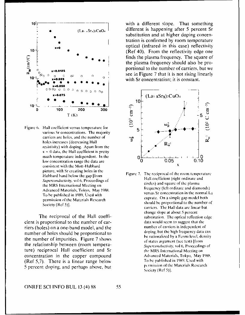
1 0 _ with a different slope. That something
• (La ,Sr.)2CuOI different is happening after 5 percent Srsubstitution and at higher doping concen-tration is confirmed by room temperature
x[0 optical (infrared in this case) reflectivity10-1,- (Ref 40). From the reflectivity edge one
. *finds the plasma frequency. The square ofE •the plasma frequency should also be pro-
2 x=.012S portional to the number of carriers, but we10__ 0 o 0 0 see in Figure 7 that it is not rising linearly
x-o.025 with Sr concentration; it is constant.
- 0000 000 00X=o.075 (Lai. xSrx)2CuO4
" • o * S • 10 1,0 100 200 300 E
T (K) E 5
Figure 6. Hall coefficient versus temperature forvarious Sr concentrations. The majority 5
carriers are holes, and the number of Xholes increases (decreasing Hall *.
resistivity) with doping. Apart from the RHx = 0 data, the Hall coefficient is prettymuch temperature independent. In the 0 0low concentration range the data are 0 0.05 0.1 0consistent with the Mott-Hubbard Xpicture, with Sr creating holes in thepicureba hSrd rati o n the Figure 7. The reciprocal of the room temperatureHubbard hand below the gap [from Hall coefficient (right ordinate andSuperconductivity, vol 6, Proceedings of circles) and square of the plasmathe MRS International Meeting onAdvanced Materials, Tokyo, May 1988. frequency (left ordinate and diamonds)To be published in 1989. Used with versus Sr concentration in the normal Lapermission of the Materials Research cuprate. On a simple gap model bothSociety (Ref 5). should be proportional to the number of
carriers. The Hall data are linear butchange slope at about 5 percent
The reciprocal of the Hall coeffi- substitution. The optical reflection edgecient is proportional to the number of car- data would seem to suggest that theriers (holes) on a one-band model, and the number of carriers is independent of
number of holes should be proportional to doping, but the high frequency data canbe rationalized by a Fermi level, dcnsilythe number of impurities. Figure 7 shows be rated byam e r lee densityof states argument (see text) Ifrom
the relationship between (room tempera- Superconductivifv vol 6, Proceedings ofture) reciprocal Hall coefficient and Sr the MRS International Meeting on
concentration in the copper compound Advanced Materials, Tokyo, May 1988.
(Ref 5,7). There is a linear range below To be published in 1989. Used with
5 percent doping, and perhaps above, but permission of the Materials ResearchSociety (Rcf 5)].
ONRFE SCI INFO BUL 13 (4) 88 55

A plasma reflection edge indepen- paired, in the high T, cuprates a large frac-dent of the number of carriers cannot be tion of the carriers are paired. Kresin et al.explain, d easily on the Hubbard-Mott show that the linear temperature depen-model. Uchida et al. (Ref 5,7,39) interpret dence of electrical resistivity in the normalthis and their other optical data as meaning phase follows from the low Fermi energythat, unlike the Hall conductivity, which is and two-dimensional nature of the phonondc, the reflection edge measures high fre- spectrum. In normal metals most of thequency response. The constancy of the thermal conductivity comes from electrons.plasma frequency is not inconsistent with But in the cuprates the low Fermi energythe model of a collapsed gap in the metallic results in the phonons being the majorphase. In this regime, the square of the channel for thermal current.plasma frequency is proportional to thesquare of the Fermi velocity times the den- HOLD THE PRESSESsity of states at the Fermi level. Dopinglowers the Fermi level and reduces the We started by apologizing for andensity of states, but this is compensated for interest in the "214" cuprate, a materialby an increase in Fermi velocity. As a result with a transition temperature of only 40 K.the plasma frequency does not depend Now as we conclude this article we have astrongly on doping concentration in the preprint from Aoki et al. (Ref 42) reportingmetallic regime. a superconducting transition at 85 to 91 K in
Once in the collapsed, metallic state La 2.CuO,.. Aoki et al. find that a small butbeyond 5 percent doping or so, we can reproducible fraction of their material isunderstand in conventional terms several superconducting both by resistivity andunusual features of the behavior of Meissner criteria. There are three distinct(La,.Sr),CuO in both the high tempera- transitions with different magnetic andture, normal phase and in thesuperconduct- resistivity signatures, at temperatures ofing phase. The key is the extremely low about 10, 40, and 90 K. In some samplesFermi energy and the highly anisotropic there is also a magnetic anomaly, a cusp inFermi surface. Kresin, Deutscher, and the susceptibility, at about 275 K.Wolf (Ref41) demonstrate this. The statesat the Fermi surface come from the planar ACKNOWLEDGMENTCu-O layers. As we have discussed, there isalmost no dispersion perpendicular to the Among other sources this articlelayers but strong in-plane dispersion in e(k). draws on two invited talks by Prof. Shin-ichiThus the Fermi surface is pipelike (but not Uchida of Tokyo University, first at a con-necessarily circular in cross section), long ference sponsored by the Society of Non-along the major axis relative to the pipe Traditional Technologies and then at theradius. The effective mass is highly aniso- Materials Research Society Internationaltropic. The Fermi energy is 0.5 eV or less. Meeting on Advanced Materials, Tokyo,Normally in metals, E. is about 10 eV. In 30 May - 3 June 1988. We benefitted fromconventional superconductors the T = 0 comments on the manuscript by Prof.gap is a small fraction of the Fermi energy Uchida and from conversations with Prof.( = 10'). In the cuprates it can be as high as K. Terakura of the Tokyo University Insti-0.1. While in normal superconductors only tute for Solid State Physics (but for thea very small fraction of the electrons are errors we get full credit).
ONRFE SCI INFO BUL 13 (4) 88 56

REFERENCES 8. T. Fujita, Y. Aoki, Y. Macno.J. Sakurai, H. Fukuba, and H. Fujii, Jpn. J.
1. J.C. Bednorz and K.A. Millier, Z. App!. Phys. 26, L-368 (1987).Phys. B 64, 189 (1986).
9. Y. Kitaoka, S. Hiramatsu, T. Kohara,2. S. Uchida, H. Takagi, K. Kitazawa, K. Asayama, K. Ohishi, M. Kikuchi, andand S. Tanaka, Jpn. J. App!. Phys. 26, LI N. Kobayashi, Jpn. J. Appi. Phys. 26, L397(1987); H. Takagi, S. Uchida, K. Kitazawa, (1987); Y. Kitaoka, S. Hiramatsu, K. Ishida,and S. Tanaka, Jpn. J. Appi. Phys. 26, L123 T. Kohara, and K. Asayama, J. Phys. Soc.(1987). Jpn. 56, 3024 (1987).
3. K. Kishio, K. Kitazawa, S. Kanbe, 10. 1. Watanabe, K. Kumagai,1. Yasuda, N. Sugii, H. Takagi, S. Uchida, Y. Nakamura, T. Kimura, Y. Nakamichi,K. Fueki, and S. Tanaka, Chem. Lett., 429 and H. Nakajima, J. Phys. Soc. Jpn. 56, 3028(1987). (1987); Y.J. Uemura et a!., Phys. Rev. Lett.
59, 1045 (1987).4. J.B. Torrance and Y. Tokura, Phys.Rev. L-ett., submitted June 1988. 11. R.M. Fleming, B. Batlogg, R.J. Cava,
and E.A. Rietman, Phys. Rev. B35, 71915. 5. Uchida, H. Takagi, S. Tajima, (1987); R.B. van Dover, R.J. Cava,K. Kishio, T. Hasegawa, K. Kitazawa, B. Batlogg, and E.A. Rietman, Phys. Rev.K. Fueki, and S. Tanaka, Superconductivity, B35, 5337 (1987).vol 6, Proceedings of the MRS InternationalMeeting on Advanced Maicl-als, Tokyo, 12. M. Onoda, S. Shamoto, M. Sato, andMay 1988 (to be published in 1989). S. Hosoya, Jpn. J. App!. Phys. 26, L363
(1987).6. K. Yamada, E. Kudo, Y. Endoh,R.J. Birgeneau, M.A. Kastner, Y. Hidaka, 13. Y. Yamaguchi, H. Yamaguchi,M. Oda, M. Suzuki, and T. Murakami, Solid M. Ohashi, H. Yamamoto, N. Shimoda,State Commun. 64, 753 (1987); S. Uchida, M. Kikuchi, and Y. Syono, Jpn. J. App!.H. Takagi, H. Yanagisawa, K. -Kishio, Phys. 26, L447 (1987); D. Vaknin,K. Kitazawa, K. Fueki, and S. Tanaka, Jpn. S.K. Sinha, D.E. Moncton, D.C. Johnston,J. App!. Phys. 26, L445 (1987); S. Mitsuda et J.M. Newsam, C.R. Safinya, and H.E. King,al., Phys. Rev. B36,826 (1987); N. Nishida et Jr., Phys. Rev. Lett. 58, 2802 (1987).al., Jpn. J. AppI. Phys. 26, L1856 (1987);G. Shirane, Y. Endoh, R.J. Birgeneau, 14. Y. Endoh, K. Yamada,M.A. Kastner, Y. Hidaka, M. Oda, R.J. Birgeneau, D.R. Gabbe, H.P. Jenssen,M. Suzuki, and T. Murakami, Phys. Rev. M.A. Kastner, C.J. Peters, P.J. Picone,Lett. 59, 1613 (1987). T.R. Thurston, J. M. Tranquada,
G. Shirane, Y. Hidaka, M. Oda,7. H. Takagi, M. Uota, Y. Tokura, Y. Enomoto, M. Suzuki, and T. Murakami,J.B. Torrance, and S. Uchida, paper in Phys. Rev. B37, 7443 (1988).preparation.
ONREE SCI INFO BUL 13 (4) 88 57

15. A. Aharony, R.J. Birgeneau, 23. A.J. Freeman, J. Yu, and C.L. Fu,A. Coniglio, M.A. Kastner, and Phys. Rev. B36, 7111 (1987); J.-H. Xu,H.E. Stanley, Phys. Rev. Lett. 60, 1330 T.J. Watson-Yang, J. Yu, and(1988). A.J. Freeman, Physics Lett. A120, 489
(1987); A.J. Freeman, C.L. Fu,16. A. Fujimori, E. Takayama- D.D. Koelling, S. Massidda, T.J. Watson-Muromachi, Y. Uchida, and B. Okai, Phys. Yang, J. Yu, and J.-H. Xu, MRS Conf.Rev. B35, 8814 (1987). Report, Spring 1987.
17. J.M. Tranquada, S.M. Heald, and 24. A.J. Freeman, J. Yu, and C.L. Fu,A.R. Moodenbaugh, Phys. Rev. B36, 5263 Phys. Rev. (Rapid Commun.);(1987). A.J. Freeman and J. Yu, Proc. of Advanced
Study Institute on Alloy Phase Stability,18. K.B. Lyons, P.A. Fleury, Crete, Greece, 14-27 June 1987;J.P. Remeika, A.S. Cooper, and A.J. Freeman and J. Yu, Proc. Intl. Conf onT.J. Negran, Phys. Rev. B37, 2393 (1987); Electronic Structure and Phase Stability inS. Sugai, S. Shamoto, and M. Sato, preprint. Advanced Ceramics, Argonne National
Laboratory, 17-19 August 1987.19. J. Gopalakrishnan, G. Colsmann, andB. Reuter, J. Solid State Chem. 22, 145 25. K.T. Park, K. Terakura, T. Oguchi,(1987). A. Yanase, and M. Ikeda, J. Phys. Soc. Jpn.
57, No. 10, 3445 (1988).20. P.W. Anderson, Science 235, 1196(1987); P.W. Anderson, G. Baskaran, 26. K. Terakura, T. Oguchi,Z. Zou, and T. Hsu, Phys. Rev. Lett. 58, A.R. Williams, and J. Kubler, Phys. Rev.2790 (1987); V.J. Emery, ibid. 58, 2794 B30, 4734 (1984).(1987); P.A. Lee and M. Read, ibid. 58,2691(1987); J.E. Hirsch, ibid. 59, 228 (1987); 27. A.FujimoriandF.Minami, Phys.Rev.S.A. Kivelson, D.S. Rokhsar, and B30, 957 (1984).J.P. Sethna, Phys. Rev. B35, 8867 (1987);D.J. Thouless, ibid. B36, 7187 (1987); 28. G.A. Sawatzky and J.W. Allen, Phys.K. Huang and E. Manousakis, ibid. B36, Rev. Lett. 53, 2339 (1984).8302 (1987); C. Gros, R. Joynt, andT.M. Rice, Z. Phys. B 68, 425 (1987). 29. T. Takahashi, F. Maeda, H. Arai,
H. Katayama-Yoshida, Y. Okabe,21. L.F. Mattheiss, Phys. Rev. Lett. 58, T. Suzuki, S. Hosoya, A. Fujimori,1028 (1987). T. Shidara, T. Koide, T. Miyahara,
M. Onoda, S. Shamoto, and M. Sato, Phys.22. J. Yu, A.J. Freeman, and J.H. Xu, Rev. B36, 5686 (1987).Phys. Rev. Lett. 58, 1035 (1987).
ONRFE SCI INFO BUL 13 (4) 88 58

30. D. van der Mare!, J. van Elp, 37. E.J.W. Verwey and P.W. Haayman,G.A. Sawatzky, and D. Heitmann, Phys. Physica (Utrecht) 8, 979 (1941);Rev. B37, 5136 (1988). E.J.W. Verwey and E.L. Hailmann, J.
Chem. Phys. 15, 174 (1947); E.J.W. Verwey,31. J.B. Torrance, Y. Tokura, A. Nazzal, P.W. Haayman, and F.C. Romeijn, ibid. 15,and S.S.P. Parkin, Phys. Rev. Lett. 60, 542 181 (1947).(1988).
38. S. Uchida, S. Tajima, H. Takagi,32. J.H. de Boer and E.J.W. Verwey, Proc. K. Kishio, T. Hasegawa, K. Kitazawa,Phys. Soc. (London) 49, 59 (1937). K. Fueki, and S. Tanaka, Proc. 18th Int.
Conf. on Low Temperature Physics, Kyoto,33. N.F. Mott, Proc. Phys. Soc. (London) 1987; Jpn. J. Appi. Phys. 26, 1105 (1987),A62, 416 (1949); Can. J. Phys. 34, 1356 Supplement 26-3.(1956); Phil. Mag. 6, 287 (1961); Advan.Phys. 16, 49 (1967). 39. S. Uchida, H. Takagi, H. Ishii,
H. Eisaki, T. Yabe, S. Tajima, and34. I.C. Slater, Phys. Rev. 82,538(1951). S. Tanaka, Jpn. J. App!. Phys. 26, L440
(1987).35. J. Hubbard, Proc. Roy. Soc. (London)A276, 238 (1963); ibid. A277, 237 (1964); 40. S. Tajima, S. Uchida, S. Kanbe,ibid. A281, 401 (1964). K. Kitazawa, K. Fueki, and S. Tanaka, Jpn.
J. App!. Phys. 26, L432 (1987).36. J.R. Cullen and E.R. Callen, Phys.Rev. B7, 397 (1973); J.R. Cullen, 41. V.Z. Kresin, G. Deutscher, andE.R. Callen, and B. Choudhury, Phys. Lett. S.A. Wolf, J. Superconductivity 3 (1988), to38A, 113 (1972); J.R. Cullen and appear.E.R. Callen, Phys. Rev. Lett. 26,236 (1971);Solid State Co1Iiiiiiu. 9, iC'4i (1971); J. 42. R. Aoki, S. Takahashi, K. Sakai,App!. Phys. 41, 879 (1970). T. Nakamura, K. Kawasaki, and R. Liang,
Parity 3, 55 (1988).
ONRFE SCI INFO BUL 13 (4) 88 59

CURRENT JAPANESE SUPERCOMPUTERSFOR COMPUTATIONAL FLUID DYNAMICSAPPLICATIONS
Hideo Yoshihara
C urrent top-of-the-line Japanese super- acquiring empirical modeling data at hyper-computers are described, stressing the sonic conditions to formulate an applicable
vector feutures significant for highly vec- transition method is discouragingly diffi-torized computational fluid dynamics cult. Such modeling data are not needed in(CFD) codes. Covered are the Fujitsu direct or large eddy simulation since theVP400E, Hitachi S820, and NEC SX-2A Navier/Stokes (laminar) equations arecomputers. A benchmarking of these com- solved directly using adequately refinedputers, scheduled in the near future, is time and space discretizations to resolve thedescribed using the Navier/Stokes calcula- turbulence.tion overadelta wing with aboutone million CFD could not serve as a usablemesh points. design tool without powerful supercom-
puters with large memories. Problems asdescribed above require enormous com-
INTRODUCTION puting times. Moreover, as flow algorithmsand supercomputers improve, the addi-
Computational fluid dynamics tional capability is used, not to reduce the(CFD) is rapidly becoming an important computer costs but to treat even more real-design tool for advanccd aerospace istic configurations with improved flowvehicles. Consider the case of the aero- modeling. The need for improved algo-spaceplane currently in design in both the rithms and computers thus does not abate.United States and Japan and in several Improvements in the algorithm must beEuropean countries. Here CFD serves not continually sought, always programmingonly as an essential design tool but as the the code in a manner best using the improv-only available tool in an important segment ing computer architecture. To be effective,of the flight where ground test facilities are the programmer must thus be familiar withincapable of producing the correct pressure the architectural features of the supercom-and temperature environment. Laminar/ puter.turbulent transitional flow also assumes a In the following, the architecturalgreatly increased role at the high altitude/ features of current supercomputers inhigh mach number portion of the flight. Japan are described with a bias towardsSince turbulence at hypersonic mach CFD applications that are highly vec-numbers is a compressible phenomenon, torizable. Here the importance of aexisting established transition theories balanced architecture must be kept in mindbased on incompressible turbulence where the size and makeup of the memory,become inapplicable. Here the direct or the memory/vector register bandwidth, thelarge eddy simulation method now assumes number and capacity of the registers, andan important role, since the alternative of the processor speed are kept compatible.
ONRFE SCI INFO BUL 13 (4) 88 61

CURRENT JAPANESE CPU contains five pipes: multiply/add/SUPERCOMPUTERS logical, add/logical, divide, mask, and load/
store. The pipes can be chained, and fourSupercomputer manufacturers in out of five pipes can operate concurrently.
Japan are Fujitsu Ltd., Hitachi Ltd., and The earlier VP400 differs from theNEC Corp. These companies are signifi- VP400E primarily in the slower processorcantly smaller than Cray Research Inc. as speed of 1.067 GF, a smaller memory ofmeasured by the number of supercom- 256 MB, and the deletion of the add/logicalputers delivered. In the following the archi- pipe chained to the multiply pipe. Both thetectural features of the top-of-the-line VP400 and VP400E have the same singleFujitsu VP400E, Hitachi S820, and NEC load/store pipe between vector registersSX-2A are given. These computers are all and memory, and this is to be contrastedsingle central processing unit (CPU) with the VP200, next lower in the FACOMmachines in contrast to current U.S. com- series, which has two (concurrent) load/puters, which are primarily multiple-CPU store pipes but with the same total band-machines. In the brief descriptions to fol- width as the VP400E. As compared to thelow, the emphasis will be on the vector VP400, the VP200 has one-half the vec-features of the supercomputers, since vis- tor processing speed but the same maincous flow CFD programs of interest are memory. For highly vectorized codes, fullhighly vectorizable. advantage of the greatly increased speed of
the VP400E cannot be fully used becauseFujitsu VP400E of the restrictive bandwidth between
memory and vector register. It would thusThe VP400E is the improved ver- appear that the VP400E was intended to
sion of the VP400 and is the most powerful be an interim machine with a greatlyin the Fujitsu FACOM series of computers, increased memory.which have been noted for their ease of use. The compiler for the VP400E is(In Japan, Fujitsu supercomputers are fully Fortran 77 compatible, and ancommonly identified by the acronym extended Fortran language, FortranFACOM standing for Fujitsu Automatic 77/VP, provides automatic vectorization ofComputer.) In Figure 1 the block diagram nested DO loops, for example, containingfor the VP400E is shown. It is a single- IF statements and gather/scatter opera-CPU machine with a processor clock time of tions. To supplement Fortran 77/VP, an7.0 nanoseconds (ns) and a peak processing additional tool, Interactive Vectorizer,speed of 1.7 gigaflops (GF). The VP400E permits the user to further tune the corn-has a 256-megabyte (MB) main memory piler interactively. (Experienced program-that can be supplemented with up to mers apparently bypass such devices.)768 MB of vector memory, that is, a total FORTUNE is a diagnostic tool detailingmemory of up to 128 megawords (MW) or the execution costs. Interactive debugginghalf of the Cray 2 basic main memory. The assist tools include TESTFORT 77 andbandwidth between memory and vector DOCK/FORTRAN 77, the latter with aregisters is 5.57 gigabytes per second full screen display.(GB/s) via a single load/store pipe. The
ONRFE SCI INFO BUL 13 (4) 88 62

| ii
9
ot
CCZ
0 LA
0~5 00J
L.-
ONRFE SCI INFO BUL 13 (4) 88 63
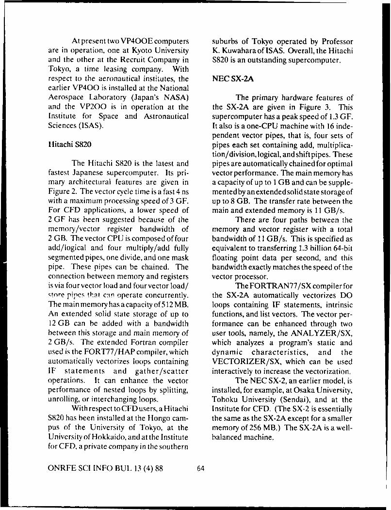
At present two VP400E computers suburbs of Tokyo operated by Professorare in operation, one at Kyoto University K. Kuwahara of ISAS. Overall, the Hitachiand the other at the Recruit Company in S820 is an outstanding supercomputer.Tokyo, a time leasing company. Withrespect to the aeronautical institutes, the NEC SX-2Aearlier VP400 is installed at the NationalAerospace Laboratory (Japan's NASA) The primary hardware features ofand the VP200 is in operation at the the SX-2A are given in Figure 3. ThisInstitute for Space and Astronautical supercomputer has a peak speed of 1.3 GF.Sciences (ISAS). It also is a one-CPU machine with 16 inde-
pendent vector pipes, that is, four sets ofHitachi S820 pipes each set containing add, multiplica-
tion/division, logical, and shift pipes. TheseThe Hitachi S820 is the latest and pipes are automatically chained for optimal
fastest Japanese supercomputer. Its pri- vector performance. The main memory hasmary architectural features are given in a capacity of up to 1 GB and can be supple-Figure 2. The vector cycle time is a fast 4 ns mented by an extended solid state storage ofwith a maximum processing speed of 3 GF. up to 8 GB. The transfer rate between theFor CFD applications, a lower speed of main and extended memory is 11 GB/s.2 GF has been suggested because of the There are four paths between thememory/vector register bandwidth of memory and vector register with a total2 GB. The vector CPU is composed of four bandwidth of 11 GB/s. This is specified asadd/logical and four multiply/add fully equivalent to transferring 1.3 billion 64-bitsegmented pipes, one divide, and one mask floating point data per second, and thispipe. These pipes can be chained. The bandwidth exactly matches the speed of theconnection between memory and registers vector processor.is via four vector load and four vector load/ The FORTRAN77/SX compiler forstore pipes that c:n operate concurrently. the SX-2A automatically vectorizes DOThe main memory has a capacity of512 MB. loops containing IF statements, intrinsicAn extended solid state storage of up to functions, and list vectors. The vector per-12 GB can be added with a bandwidth formance can be enhanced through twobetween this storage and main memory of user tools, namely, the ANALYZER/SX,2 GB/s. The extended Fortran compiler which analyzes a program's static andused is the FORT77/HAP compiler, which dynamic characteristics, and theautomatically vectorizes loops containing VECTORIZER/SX, which can be usedIF statements and gather/scatter interactively to increase the vectorization.operations. It can enhance the vector The NEC SX-2, an earlier model, isperformance of nested loops by splitting, installed, for example, at Osaka University,unrolling, or interchanging loops. Tohoku University (Sendai), and at the
With respect to CFD users, a Hitachi Institute for CFD. (The SX-2 is essentiallyS820 has been installed at the Hongo cam- the same as the SX-2A except for a smallerpus of the University of Tokyo, at the memory of 256 MB.) The SX-2A is a well-University of Hokkaido, and at the Institute balanced machine.for CFD, a private company in the southern
ONRFE SCI INFO BUL 13 (4) 88 64

KIE>
CC
u ri
EF7R
o s~I
ONRFE SCI INFO BUL 13 (4) 88 65
.. . .- l m Iu u m mm m Im

AaOU
o ,
00
C-2 1! , 0
ONRFE SCI INFO BUL 13 (4) 88 66
I-

FINAL REMARKS The Japanese computer firms up tothe present have not strongly promoted
All three Japanese supercomputers sales outside Japan. This is changing. In theare without question outstanding com- Fujitsu VP400E, Hitachi S-820, and NECputers with large memories and speeds in 2XA, the operating systems have beenthe gigaflop range. made UNIX compatible, in part for the U.S.
For these single-CPU machines, the market. Moreover, the new computers tophenomenal peak processor speeds have be announced by Fujitsu and NEC in thebeen achieved by using many concurrent near future are rumored to be multiproces-pipes in the vector processor. Computa- sor machines, again suggesting a targetingtional rates for a given CFD problem, of U.S. markets. (Rumors are prevalenthowever, cannot approach such speeds since Japanese supercomputer companiesunless the vector processing pipes are kept are reluctant to announce new productscontinuously filled. This requires an algo- until both hardware and software have beenrithm with a high degree of vectorization, a fully checked out.)sufficiently large versatile memory, and a In the near future, a benchmarkingnonconstricting bandwidth between of the above Japanese supercomputers willmemory and processor including compati- be carried out. Instead of the usual comput-ble vector registers. ing kernels, a three-dimensional Navier/
The single-CPU Japanese com- Stokes calculation over a delta wing will beputers are in contrast to current multi-CPU used with a mesh of about one millionU.S. suvercomputers such as the Cray YMP points. This approach was taken since thecomputer with eight CPUs, each processor use of the Navier/Stokes code will not onlyhaving two add/subtract, two logical, one exercise all aspects of the computer but willshift, one multiply, and one reciprocal pipe. yield valuable information on a code thatThis difference in architectural approach willbe widely used in the coming decade. Inmaybeexplainedinpartbythedifferencein a benchmark exercise, the merits of thethe user environment. In Japan the number supercomputer and the skill of the program-of users performing large-scale computa- mer must be carefully distinguished.tions is significantly less than in the United Benchmarks will therefore be obtained forStates, and the fast single-CPU machines two cases: the first for the Navier/Stokesare sufficient, at least for the immediate code as furnished, and the second with coderequirements. On the other hand, in the modifications permitted by the participantsUnited States with a much larger number of to improve the performance. Fortran-users carrying out large computations, a compatible compiler tuning will be per-multiple-CPU machine is more suitable, mitted. Timing breakdowns will be noted,since the many users can be accommodated forexample, for the CPU time, data transferusing the CPUs independently. Moreover, times, as well as the input/output (I/O)for users with very large problems (that is, time for throughput assessment. Each par-hundredsofhoursofcomputing),theCPUs ticipant will describe the code improve-can be used in appropriate combinations ments and compiler tuning used.through multitasking to reduce the comput-ing time to a more responsive level.
ONRFE SCI INFO BUL 13 (4) 88 67
Cray Research Japan Inc. has also ACKNOWLEDGMENTSagreed to participate in this benchmarkingusing the 8-CPU Cray YMP. The bench- Discussions with Dr. Yoshio Tago,mark results of the above Japanese super- manager of the Scientific Systemls Engi-computers and the Cray YMP will be corn- neering Group of Fujitsu Inc.; Mr. Shunpleted in early 1989. It is anticipated that Kawabe, senior engineer of the Computerbenchmarks for the rumored new super- Development Department of Hitachi Inc.;computers from Fujitsu and NEC will be and Mr. Shinichi Mineo, supervisor of thecompleted during the summer of 1989. Third Systems Support Department of the
There are pitfalls in the benchmark- NEC Corp., are gratefully acknowledged.ing process for supercomputers. Thus by Mr. Yoshikazu Hori, president of Crayitself, a performance comparison of the Research Japan Inc., kindly provided infor-single-CPU (but many piped) Japanese mation on the Cray YMP.supercomputers with the 8-CPU Cray YMPor in a reverse sense with the Cray YMP Hideo Yoshihara arrived in Tokyo inwith a single CPU is meaningless. In select- April 1988fora2-vearavsignment as a liaisoning a computer, factors other than a bench- scientistforthe Office of Naval Research. Hismark clearly must be taken into account, assignment is to follow the progress ofsuch as the cost of the computer and its user advanced supercomputers and to review andenvironment. However, of more impor- assess the viscous flow simulation research intance to the CFD community are the the FarEast. Dr. Yoshiharaformerly wa withmethod and approach used in the compiler the Boeing Company, where lie was Engineer-tuning and code improvements by the par- ing Manager for Applied Computationalticipating programming experts. Aerodynamics. He was als an affiliate pro-
The above benchmark exercise will fessor in the Department of Aeronautics andbe ajoint effort with Professor K. Fujii of the Astronautics of the University of Washington,Institute of Space and Astronautical an A IAA Fellow, andafonnrmerinmheroftheSciences who will provide his Navier/ FluidDynamics Pa'l of AGARD/NATO.Stokes code, the geometry, and mesh for thedelta wing.
ONRFE SCI INFO BUI. 13 (4) 88 68
.. .. MMel m ~ l I I / I l~ I I

INTERNATIONAL SYMPOSIUM ONSTRATEGY OF INNOVATION INMATERIALS PROCESSING (SIMAP '88)
E.A. Metzbower
A t the International Symposium on 1. Creation and Processing of High Func-Strate&y' of Innovation in Materials tion Materials
Processing, the sessions reflected the depthand breadth of the research efforts at the 2. Surface ModificationWelding Research Institute. These sessionswere in the following areas: creation and 3. Biomaterialsprocessing of high function materials, sur-face modification, biomaterials, new join- 4. New Joining Processes for Advanceding processes for advanced materials, utili- Materialszation of computers, and future structures.
5. Utilization of Computers
An international symposium on 6. What We Can Do for the Future Struc-Strategy of Innovation in Materials Pro- turescessing--New Challenge for the 21stCentury (SIMAP '88) was held 17 and The symposium started with an18 May 1988 at the newly dedicated Arata excellent presentation by Professor JulianHall of the Japanese Welding Research Szekley of the Massachusetts Institute ofInstitute at Osaka University. Professor Technology titled "New Developments inEmeritus Yoshiaki Arata, in the preface to Speciality Metals Processing--The Role ofthe symposium proceedings, states that his the Science Base." Prof. Szekley used thehope is that "many people will participate "S" curve as a means of describing thein this symposium to study the state of the relationship between effort and perfor-arts, to discuss the future trends, and to mance. The "S" curve has a lower shelf orvisualize strategy for innovation in mate- level followed by a rapid transition to anrials processing among people not only in upper shelf or level. Using this device heJapan but also world wide." The sympo- indicated that certain technologies, e.g.,sium was attended by over 200 people with electroslag remelt (ESR), vacuum arcabout 40 of these from outside of Japan. remelt (VAR), plasma arc remelt (PAR),
The six sessions of the symposium had reached the top of the curve and only areflected the depth and breadth of the small increase in performance could beresearch efforts at the Welding Research obtained for any increase in effort. On theInstitute. The six sessions were as follows: other hand, such technologies as spray
ONRFE SCI INFO BUL 13 (4) 88 69

forming and plasma cold hearth remelting The session on surface modificationare in the center of the curve and a large began with a presentation by Professorincrease in performance could be obtained H.D. Steffens of the University offor any increase in effort. Other technolo- Dortmund titled "Arc and Plasma Sprayinggies, such as composites and cold crucible Today and in the 90th." Prof. Steffensinduction melting, are on the bottom shelf reviewed the area of coatings by sprayingof the "S" curve and considerable effort will techniques, concentrating on current andbe required to enhance their performance. future applications. In view of the continu-Obviously performance and effort are ally increasing construction materialparameters that could easily be replaced by requirements and the increasing expense ofa host of other parameters such as utiliza- materials with special properties such astion and time. This concept was then high resistance to corrosion and wear, ther-applied to plasma systems, melt behavior, mal spraying methods, such as plasma andatomization, and solidification processing. arc spraying, are becoming more and more
During my presentation on "The important. In his paper, Prof. SteffensRole of Lasers in Modern Materials Pro- reviewed the operating principles, currentcessing," I reviewed the use of high power, and future application fields, as well as thecontinuous wave lasers in materials pro- latest operational variants of thesecessing and indicated areas in which lasers methods.are expected to contribute significantly in Dr. Muryel Wehr, Centre dethe near and far future both by modifica- Recherches de la Compagnie Generaletions and improvement in lasers as well as a d'Electricite, gave the next presentation onbetter understanding and use of the laser as the "Formation of Ceramic Coatings bya unique heat source. Laser Processes." In this work, in which
Professor R. Yamamoto from the Dr. Wehr collaborated with ProfessorUniversity of Tokyo gave the next presenta- A. Matsunawa of the Welding Researchtion titled "Superlattices and Their Appli- Institute, the different techniques used forcations." The presentation centered on the the formation of ceramic coatings with aproduction and properties of multilayered Nd:YAG laser as a heat source werefilms or artificial superstructure films. The described as well as the present and pro-control of such films is almost on the atomic jected use of these coatings. Dr. Wehrscale and the creation of these films appears concluded that for wear applications, pow-to be a time consuming and experimentally der deposition methods, pyrolytic laserdifficult process. The author states that "at chemical vapor deposition (LCVD), andpresent it is not clear which material and laser pressure vapor deposition (LPVD)fabrication parameters determine the are the most appropriate. The LPVD pro-growth and propertiesofasuperstructure in cess allows the deposition of all types ofa certain metal." Clearly this technology ceramics, while the LCVD process is onlyhas a long way to go before it is used com- possible for materials having gas or highmercially. pressure liquid reactant sources.
ONRFE SCI INFO BUL 13 (4) 88 70

The concluding paper in this session surgical uses. Among the projected uses ofwas "Formation of High Function Ceramic hydroxypatite are: artificial bones andSurface by Ion Implantation," by Professor joints, bone filler, artificial blood vesselsN. Iwamoto, the director of the Welding and tracheal, dentifries, tooth root, andResearch Institute. Prof. Iwamoto teeth. His presentation was highlighted bydescribed his research to fabricate a a set of excellent color slides of the clinicalSiC-SiN composite material using the ion trials.implantation technique with nitrogen ions. Session 4 was on new joining pro-He concluded that migration of nitrogen cesses for advanced materials. The firstinside the implanted volume occurred after presentation, by Professor David Dickinsonheat treatment and that depending on :he of Ohio State University, was titled "Futureimplanting condition, the occurrence of the Trends for Joining of Advancedformation of carbonitride was detected, but Materials--A Report on Researchthat the heat treatment temperature was Activities in Advanced Materials andcritical. Processes at Ohio State University." Prof.
The concluding session of the day Dickinson gave a thorough overview of thewas on biomaterials. In the first paper, many different research programs in the"Recent Progress on the Science of Bio- Welding Engineering Department at Ohiomedical Polymeric Materials," Professor State aimed at using advanced materialsK. Takemoto of Osaka University gave an and advanced joining processes. Theenlightening presentation on the biomedi- challenge that the 21st century offers tocal polymeric materials that have been industry, to effectively use the newerdeveloped, especially focusing on contact advanced materials and processes tolenses, dental polymers, artificial skin, liver, produce better, more economical weldedkidney, heart, etc. The problems associated and bonded products at reduced costs, waswith their uses were also discussed. The a recurring message in the presentation.emphasis in this review was on materials Dr. C.J. Thwaites from the Interna-that have been fully developed. The mate- tional Tin Research Institute, U.K., gave anrials were divided into three areas: interesting presentation on "Soldering(1) biomedical polymeric materials that Microelectronic Assemblies: Some Prob-have little contact with blood, such as lems and Studies." This seemingly mun-contact lenses; (2) materials that are in dane field has some unique problems asso-contact with blood but only for a short time, ciated with it, and as was pointed out, verysuch as artificial kidneys; and (3) materials little basic research is being done in thisthat are in contact with blood for long area. There is, however, a program in thisperiods of time, such as an artificial heart. field at the Welding Research Institute
Professor H. Aoki of the Tokyo under Professor Okamoto. Dr. ThwaitesMedical and Dental University presented a pointed out that the provision of highlypaper titled "Hydroxyapatite of Great solderable surfaces of component termina-Promise for Biomaterials," in which he tions and circuit boards is still a primarydescribed some clinical experiments on requirement for reliability. Checking ofdogs using hydroxyapatite for dental and solderability of components is desirable,
ONRFE SCI INFO BUL 13 (4) 88 71

but methods for this have not been per- presentation delved into such items asfected because of the small size of the scalar versus vector processing and thecomponents. Visual inspection is becoming many applications of supercomputers inextremely difficult, if not impossible, and today's research. Improvements in thereliance must therefore be placed on using speed of supercomputers are limitedsurfaces of good solderability and close because of the propagation speed of ancontrol of the soldering processes. electronic pulse in a wire. One direction for
Professor E.R. Wallach of future systems is multiprocessors. TheCambridge gave an excellent talk on difficulty with that approach is the"Progress of Diffusion Bonding of Various development of efficient software.Materials," in which the various proposed The last presentation in this sessionmechanisms of diffusion bonding were was by Professor J.L. Pan of Tsinghua Uni-reviewed and the different models of the versity, China, on the "Future Direction ofprocess were discussed. Diffusion bonding Welding Structure Production." Theis finding increased industrial applications author pointed out the relationshipin joining such diverse materials as super- between steel production and the mostplastic metallic alloys, metal matrix com- prosperous industries of developedposites, and the new high critical tempera- countries in different ages and stated thatture ceramic superconductors. Bond welding will play an important part in heavyassessment by mechanical testing and non- industries for many years to come. Thedestructive evaluation as well as micros- automation of these processes is critical.copy of the joint area was also discussed. The development of computer-aided
"Utilization of Computers" was the design (CAD), computer-aided manufac-title of the fifth session. The first presenta- turing (CAM), and the sensing devices thattion was on "Color Vision for Road Follow- can be instrumented to the computer willing," by Professor C. Thorpe of Carnegie lead to a true artificial intelligence (AI) forMellon University. Prof. Thorpe talked welding.about the problems involved with the Session 6 was titled "What We Cansensing of a road and directing a vehicle Do for the Future Structures." Dr.over the correct path in real time. The P.R. Kasten of Oak Ridge Nationalinterpretation of the path and the problems Laboratory presented "Very Highassociated with such things as shadows, Temperature Reactors for Future Use," insnow, rain, etc. were well covered in this which he described the concept of modularinteresting presentation. Parallel process- reactors and how they could be improved bying has been incorporated into the compu- raising the temperature so that theirtational scheme. efficiency is greatly improved. The material
The next presentation was titled problems associated with these reactors"The Trends in Supercomputers," by were stressed. At these higherMr. M. Maruyama of Century Research temperatures fossil fuel conversion can beCenter, Japan. This technically oriented used.
ONRFE SCI INFO BUL 13 (4) 88 72

Dr. A. Kitamura from Ishikawajima- "Magnetically Levitated Vehicles by Super-Harima Heavy Industries presented "Of conducting Magnets." This prototype sys-Present and Future Space Structures, Their tern has been developed to propel a railroadMaterials and Construction." This paper car at speeds up to 300 km/h.stressed the need to develop new light-weight materials that can be used for space Edward A. Metzboweris a supervisorystructures. metallurgist in the Materials Science and
The symposium went from outer Technology Division of the Naval Researchspace to the depths of the oceans with the Laboratory (NRL) in Washington, DC. Apresentation titled "Materials for Deep graduate of Loyola College and the JohnsSubmergence Research Vehicle" by Dr. Hopkins University, Dr. Metzbower has beenK. Yokota of Mitsubishi Heavy Industries. employed at NRL since 1967. Currently, asDr. Yokota discussed the material head of the Welding Metallurgy Section, heisproblems associated with the design and involved in a program studying tte relation-construction of SHINKAI 2000, a ships between the mechanical properties,submergence research vehicle that can micro- and macro-structures, and processingoperate at depths up to 2,000 meters, and its parameters of laser beam welding. He is asuccessor under construction, a fellow of the Welding Institute, on the Boardsubmergence research vessel that can go as of Directors of the Laser Institute ofAmerica,deep as 6,000 meters. The primary metal in chairman of the Electron and Laser Beamthe hull is a titanium alloy (Ti-6AI-4V ELI). Committee of the Joining Division Council of
The final presentation at the sympo- ASM International, and a member of thesium was by Mr. H. Nakashima of the Rail- High Density Cutting and Welding Commit-way Technical Research Institute on tee of the American Welding Society.
ONRFE SCI INFO BUL 13 (4) 88 73

INTERNATIONAL MEETINGS IN THE FAR EAST
1989-1994
Compiled by Yuko Ushino
Yuko Ushino is a technical information specialist for ONR Far East. Shereceived a B.S. degree from Brigham Young University at Provo, Utah.
The Australian Academy of Science, the Japan Convention Bureau, and the ScienceCouncil of Japan are the primary sources for this list. Readers are asked to notify us of anyupcoming international meetings and exhibitions in the Far East which have not yet beenincluded in this report.
1989
Date Title/Attendance* Site Contact for Information
January International Conference on Calcutta, Suprokash Mukherjee3-9 Nuclear Reaction Mechanism India Saha Institute of Nuclear Physics
Sector 1, Block AF, Bidhan NagarCalcutta 700 064
January The 5th International Bombay, Professor C.M. Srivastava, Head10-13 Conference on Ferrites India Advanced Center for Research in
Electronics (ACRE)
Indian Institute of Technology (IIT)Bombay 400076
January National Conference on Trivandrum,19-20 Industrial Tribology-89 India
January The 2nd NCB International New Delhi, The Organizing Secretary30- Seminar on Cement and Building India 2nd NCB International SeminarFebruary Materials National Council for Cement and Building3 Materials
M 10 South Extension IIRing Road, New Delhi 110049
January The 17th Australian Brisbane, Dr. D.J.T. Hill31- Polymer Symposium Australia Chemistry DepartmentFebruary University of Queensland3 Brisbane 4067 QLD
February International Symposium on Tamilnadu, Dr. S. Guruviah1-5 Industrial Metal Finishing India Central Electrochemical Research
Institute
Karaikudi 623006Tamilnadu, India
*Note: Data format was taken from the Japan International Congress Calendar
published by the Japan Convention Bureau.
No. of participating countriesF: No. of overseas participants
J: No. of Japanese participants
ONRFE SCI INFO BUL 13 (4) 88 75

1989
Date Title/Attendance Site Contact for Information
February Advances in Biomedical Perth, The Secretary, W.A. Polymer Group5-6 Polymers Australia Royal Australian Chemical Institute
125 Hay StreetPerth, WA 6000Australia
February International Conference on Jamshedpur, Secretariat: BMT-898-10 Base Metals Technology India c/o Mr. D.D Akerkar
Deputy DirectorNational Metallurgical LaboratoryPO Burmanines. Jamshedpur 831007
February The 4th International Sydney, Secretariat14-17 Photovoltaic Science and Australia 2 New McLean Street
Engineering Conference P.O. Box 79NSW 2027
March International Symposium/ Takamatsu, Department of Physiology12-16 Information Transduction and Japan Kagawa Medical School
Processing in Biological 1750 Ikenobe, Miki-choSystems - From Cell to Kita-gun, Kagawa-ken 761-07Whole Body
8-FEO-J190
March The Ist J71PS international Tokyo, Japan Hydraulics and Pneumatic Society14-16 Symposium on Fluid Power Japan 3-5-8 Shiba-koen
Minato-ku, Tokyo 1055-F50-J'00
March International Workshop on Tsukuba, Secretariat: International Workshop on15-17 Intelligent Materials Japan Intelligent Materials
The Society of Non-Traditional Technology
Toranomon Kotohira-Kaikan B1ig, 3F1-2-8 ToranomonMinato-ku, Tol'yo 105Attn: Mr. Tsunehisa Kurino
April International Symposium for Nagoya, Institute of Industrial Science3-5 Electromachining Japan University of Tokyo
7-22-1 Roppongi16-F100~J300 Minato-ku, Tokyo 106
April IFIP TC-2 Working Conference Tokyo, Professor Tosiyasu L. Kunii3-7 on Visual Database Systems Japan Department of Information Science
Faculty of Science, University of Tokyo15-F30-J60 7-3-1 Hongo
Bunkyo-ku, Tokyo 113
April International Workshop on Tokyo, Professor Mitsuru Ishizuka10-12 Industrial Applications of Japan Institute of Industrial Science
Machine Intelligence and University of TokyoVision (MIV-89) 7-22-1 Roppongi
Minato-ku, Tokyo 106
April The International Symposium Undecided The Institute of Electrical Engineers10-13 for Electromachining of Japan
Gakkai Center Building15-FIO0-J300 2-4-16 Yayoi
Bunkyo-ku, Tokyo 113
April 1989 National Engineering Perth,10-14 Conference Australia
April International Conference on Beijing, ICMSR Secr-tariat10-15 Modernization of Steel Rolling People's Chinese Society of Metals
Republic 46 Dongsixi .ajieof China Beijing
ONRFE SCI INFO BUL 13 (4) 88 76

1989
Date Title/Attendance Site Contact for Information
April International Symposium Shanghai, International Symposium on Ship11-14 on Ship Resistance and People's Resistance and Powering Performance
Powering Performance (ISRP) Republic Department of Naval Architectureof China and Ocean Engineering
Shanghai Jiao Tong UniversityShanghai
April International Symposium for Nagoya, Japan Society of Electrical-Machining11-14 Electro-machining (ISEM 9) Japan Engineers
c/o Institute of Industrial Science16-F50-J300 University of Tokyo
7-22-1 RoppongiMinato-ku, Tokyo 106
April The 5th International Meeting Kyoto, Professor T. Matsuda11-14 of the Polymer Processing Japan Research Center for Medical Polymers and
Society BiomaterialsKyoto UniversityShogoin, Sakyo-ku, Kyoto
April The 22nd JAIF Annual Tokyo, Japan Atomic Industrial Forum, Inc.12-14 Conference Japan Toshin Bldg
1-1-13 Shimbashi25-F150-J1,100 Minato-ku, Tokyo 105
April The 2nd Asian Fisheries Tokyo, Secretariat: The 2nd Asian Fisheries Forum18-21 Forum Japan c/o Faculty of Agriculture
Tokyo University30-F150-J150 1-1-1 Yayoi
Bunkyo-ku, Tokyo 113
April The 4th Wire Asia, Shanghai, Exhibitions for Industry Ltd.23-27 Conference and Exhibition People's 110-112 Station Road East
Republic Oxted, Surrey RH3 OQA, UKof China
April The 4th International Tsukuba, Dr. Kiroo Nakahara24-29 Conference on Langmuir-Blodgett Japan Secretary General of 4th-LB Conference
Films Saitama UniversityUrawa 338
NA-F150-J300
April The 9th International Tokyo, Member/Customer Service25-28 Conference on Nondestructive Japan AF! Tr'-ernational
Evaluation in the Nuclear OH 44073 U.S.A.Industry
April International Symposium on Seoul, Dr. Byung-Koo Kim26-28 Pressure Vessel Technology Korea Korea Advanced Energy Research Institute
and Nuclear Codes & Standards P.O. Box 7Daeduk-Danji, Chungnam, Korea 301-353
May The 2nd IMEKO TC 14 Beijing,9-12 International Symposium on People's
Metrology for Quality Control Republicin Production of China
May International Conference on Beijing, Professor Ji-Gao Zhang9-12 Electrical Contacts and People's Beijing University of Posts and
Electromechanical Components Republic Telecommunicationsof China P.O. Box 109
Beijing
May The 3rd World Conference Osaka, Research Reactor Institute, Kyoto University14-18 on Neutron Radiography Japan Kumatoricho, Sennan-gun, Osaka 590-04
ONRFE SCI INFO BUL 13 (4) 88 77

1989
Date Title/Attendance Site Contact for Information
May The 10th International Kyoto, Mr. T. Kurino17-19 Workshop on Rare-Earth Japan c/o The Society of Non-Traditional
Magnets and Their Applizaticns TechnologyToranomon Kotohira Kaikan Bldg, 3F1-2-8 ToranomonMinato-ku, Tokyo 105
May The 3rd Co,C, erce of Yokohama, Professor Koji Shimizu18-20 Asian-Pacific Congress on Japan Department of Mechanical Engineering
Strength Evaluation Faculty of Engineering
Kanto Gakuin University4834 Mutsu-uraKanazawa-ku, Yokohama 236
May International Conference on Tokyo, Japan Society of Mechanical Engineers21-24 Advanced Mechatronics Japan Sanshin Hokusei Bldg
2-4-9 YoyogiShibuya-ku, Iokyo 151
May 1989 SymposIuM on VLSI Kyoto. Secretariat22-25 Technology Japan c/o Business Center for Academic Societies
Japan
Conference Department3-23-1 Hon:goBunkyo-ku, Tokyo 113
May The 7th Frnrih-Japanese Kurashiki, French-Japanese Scclety for Medicinal and22-25 Symposium on Medicinal and Japan Fine Chemistry
Fine Chemistry c/o Faculty of PharmacologyHokkaido University
2-F30-JR0 Nishi-6, Kita-12Kita-ku, Sapporo 060
May 1989 Symposium on VLSI Kyoto, Secretariat25-27 Circuits Japan c/o Business Center for Academic Societies
JapanConference Department3-23-1 HongoBunkyo-ku, Tokyo 113
May 1989 r.!ernational Zvmposiiim Guangzhou, Dr. D.M. Miller29-31 on Mul:ple-Valied Lugi: People's Department of Computer Science
(ISMVL-s9 Republic University of Victoriaof China P 0. Box 1700
Victoria, B.C., Canada V8W2Y2
May The 2nd International Near Tsukuha, Dr. Sumio Kawano29- Infrared Sereacopy Japan National Food Researchi InstituteJune Conference Kannondai, Tsukuba 305
2
June Internatioial Symposion' on Eeij ing,5-8 Thermodynamic Analysis anl People's
Improveme!.t of Energy Systems Republicof China
June IFIP WGI, 2 Working Conference Tokyo, Professor Gotaro Odawara6-7 on the CAl iyctem; Using A
l Japan c/o Business Center for Academic Societies
Techni ',-s Japan3-23-1 Hong,
Bunkyo-ku, Tokyo 113
June The XXI I Ya'cada Conferenr- cn Toyonaka. Professor Masato Morita12 15 N clpar Weak P- - oss ail 7apan 1-1 Machi kaneyara-Cho
Nuclear Strut,ir. Toyonaka-shi. Osaka 50
ONRFE SCI INFO BUI. 13 (4) 88 78

1989
Date Title/Attendance Site Contact for Information
June IUPAC International Symposium Seoul, Professor Sung Chul Kim26-28 on Molecular Design of Korea Department of Chemical Engineering
Functional Polymers KAISTP.O. Box 131Cheongyang, Seoul, Korea
July The 27th International Gold Coast, UniQuest Limited2-7 Conference on Coordination Australia University of Queensland
Chemistry St. Lucia, Queensland 4067
July XXVII International Brisbane, Professor Clifford J. Hawkins2-7 Conference on Coordination Australia Department of Chemistry
Chemistry University of Queensland
Saint Lucia, Brisbane, Queensland 4067
July 1989 International Micro Kobe, Secretariat3-5 Process Conference (Micro Japan c/o Business Center for Academic Societies
Process '89) JapanConference Department3-23-1 HongoBunkyo-ku, Tokyo 113
July ICOMAT '89: The 6th Sydney, ICOMAT '893-7 International Conference for Australia c/o N.F. Kennon
Martensitic Transformations Department of Metallurgy and MaterialsEngineering
University of WollongongP.O. Box 1144Wollongong, NSW 2500, Australia
July International Conference on Beijing, Professor Sun Peimao5-8 Opto-Electronics Science and People's Department of Precision Instruments
Engineering (ICOESE) Republic Tsinghua Universityof China Beijing 100084
July Internati-il Conference on Nangjing, Professor Wai-Kai Chen6-8 Circuits and Systems (ICCAS '89) People's Department of Electrical Engineering and
Republic Computer Scienceof China University of Illinois at Chicago
P.O. Box 4348Chicago, IL 60680
July The 4th International Oharai, Professor Osamu9-14 Conference on Scanning Japan Faculty of Science
Tunneling Microscopy/ Tokyo Institute of TechnologySpectroscopy (ICSTM/STS) 2-12-1 Ohokayama
Meguro-ku, Tokyo 152
July The 4th International Kyoto, IOPB Symposium10-14 Symposium of Plant Japan c/o Department of Botany
Biosystematics (IOPB) Faculty of Science, Kyoto UniversityKitashirakawa Oiwake-cho
30-F80-J200 Sakyo-ku, Kyoto 606
July The 8th International Congress Tsukuba, Y. Nozawa10-17 of Proto-Zoology Japan Department of Biochemistry
Gifu University40 Tsukasamachi
Gifu 500
July The 1st China-Japan Beijing, Professor Huang Jun-Qin11-14 International Symposium on People's Department of Automatic Control
Instrumentation, Measurement Republic Beijing University of Aeronautics andand Automatic Control of China Astronautics
Beijing 100083
ONRFE SCI INFO BUL 13 (4) 88 79
I. ... .. ... ........... . . . - -- . l n n u n i ur m nm

1989
Date Title/Attendance Site Contact for Information
July Topical Meeting on Solid Beijing, Professor Ue Peida12-14 State Lasers People's University of Beijing
Republic Post and Telecommunicationsof China Beijing
July The 8th International Kyoto, Dr. Toyoaki Miyagawa17-20 Conference on Alkali Japan 8th ICAAR
Aggregate Reaction (8th The Society of Materials Science, JapanICAAR) 1-101 Yoshida Izumidono-cho
Sakyo-ku, Kyoto 606
July The 9th International Beijing, Professor T.S. Ke17-20 Conference on Internal People's Laboratory of Internal Friction and
Friction and Ultrasonic Republic Defects in SolidsAttenuation in Solids of China Institute of Solid State Physics(ICIFUAS 9) Academia Sinica
Hefei
July The 7th International Kobe, 7th International Conference on18-21 Conference on Integrated Japan Integrated Optics and Optical Fiber
Optics and Optical Fiber Communication (IOOC '89)Communication (IOOC '89) cio Business Center for Academic Societies
Japan
3-23-1 HongoBunkyo-ku, Tokyo 113
July The International Conference Chongquing,20-22 on Machinery Moving Accuracy People's
(Theory & Measurement) Republicof China
July The 2nd Microoptics Tokyo, Mr. Yasuhiko Noguchi24-26 Conference/The 9th Japan Secretariat: MOC/GRIN '89
Topical Meeting on Banda BuildingGradient-Index Imaging 1-35-5 YoyogiSystems (MOC/GRIN '89) Shibuya-ku, Tokyo 151
July The 2nd International Tsu, Mie, Professor Masataka Tokuda31- Symposium on Plasticity and Japan Faculty of EngineeringAugust Its Current Applications Mie University4 1515 Kamihama-cho
20-F70-J70 Tsu, Mie 514
August International Conference on Chongquing,11-13 Constitutive Laws for People's
Engineering Materials Republicof China
August Solar Energy Congress Tokyo, Japanese Section of International Solar13-18 Tokyo 1989 Japan Energy Society
322 San Patio40-F600-J400 3-1-5 Takada-no-baba
Shinjuku-ku, Tokyo 160
August The 4th Asian Congress Hong Kong Professor N.W.M. Ko19-23 of Fluid Mechanics 4ACFM Secretariat
c/o Department of Mechanical EngineeringUniversity of Hong KongPokfulam Road, Hong Kong
August The 6th International Osaka, Chemical Society of Japan20-25 Symposium on Novel Aromatic Japan 1-5 Kanda-Surugadai
Compounds (ISNA-6) Chiyoda-ku, Tokyo 101
20-FI00-J300
ONRFE SCI INFO BUL 13 (4) 88 80

1989
Date TitLe/Attendance Site Contact for Information
August The 9th International Sendai, Secretariat: 9th International Conference on20-25 Conference on Crystal Japan Crystal Growth
Growth (ICCG) c/o Inter Group Corp.8-5-32 Akasaka
48-F250-J550 Minato-ku, Tokyo 107
August The 14th International Tsukuba, Mr. Kitagawa21-26 Conference on High Energy Japan National Laboratory for High Energy Physics
Accelerators 1-1 OohoTsukuba-shi, Ibaraki 305
August 1989 International Symposium Tokyo, Dr. Takashi Katagi22-25 on Antennas and Propagation, Japan Mitsubishi Electric Corp.
Japan (ISAP '89) 325 KamimachiyaKamakura 247
August The 10th International Takayama, Dr. Tetsuo Asaji22-26 Symposium on Nuclear Japan The Secretary of Xth ISNQRS
Quadrupole Resonance Department of Chemistry, PC IISpectroscopy Faculty of Science
Nagoya UniversityChikusa, Nagoya 464-01
August The 7th Internetional Beijing, Tu Dezheng25-28 Conference on Composite People's China Society of Aeronautics and
Materials (ICCM-7) Republic Astronauticsof China 67 South Street
Jiao Daokou, Beijing
August The 7th International Summer Zao. Professor H. Kjmatsu26-31 School on Crystal Growth Japan ISSCG-7 Chairperson
c/o Inter Gro,:p Corp.Akasaka Yamakatsu Bldg8-5-32 AkasakaMinato-ku, Tokyo 107
August The 3rd International Tokyo, Professor H. Ezawa27-31 Symposium on Foundation of Japan Department of Physics
Quantum Mechanics--In the Gakushuin UniversityLight of New TechnoLogy Mejiro, Toshima-ku, Tokyo 1,1(ISQM-Tokyo '89)
NA-F50-J60
August The 5th International Kyoto, Organizing Committee of 5th International27- Symposium on Microbial Japan Symposium on Microbial EcologySeptember Ecology (5th ISME) c/o Inter Group Corporation1 8-5-32 Akasaka
73-F600-J600 Minato-ku, Tokyo 107
August International Symposium on Nagoya, Professor Michiru Yasuhara28-31 Computational Fluid Dynamics-- Japan Department of Aerospace Engineering
Nagoya, 1989 (ISCF-Nagoya 1989) Nagoya UniversityFuro-cho, Chikusa-ku, Nagoya 464-01
August The 5th International Tokyo, Department of Mechanical Engineering28-31 Symposium on Robotics Research Japan Faculty of Engineering
University of Tokjo7-3-1 HongoBunkyo-ku, Tokyo 113
August The Ilth International Tsukuba. T. Haruyama28- Conference on Magnet Japan National Laboratory for High Energy PhysicsSeptember Technology Oho-machi, Tsukuba-shi, Ibaraki 305
N
ONRFE SCI INFO BUL 13 (4) 88 81
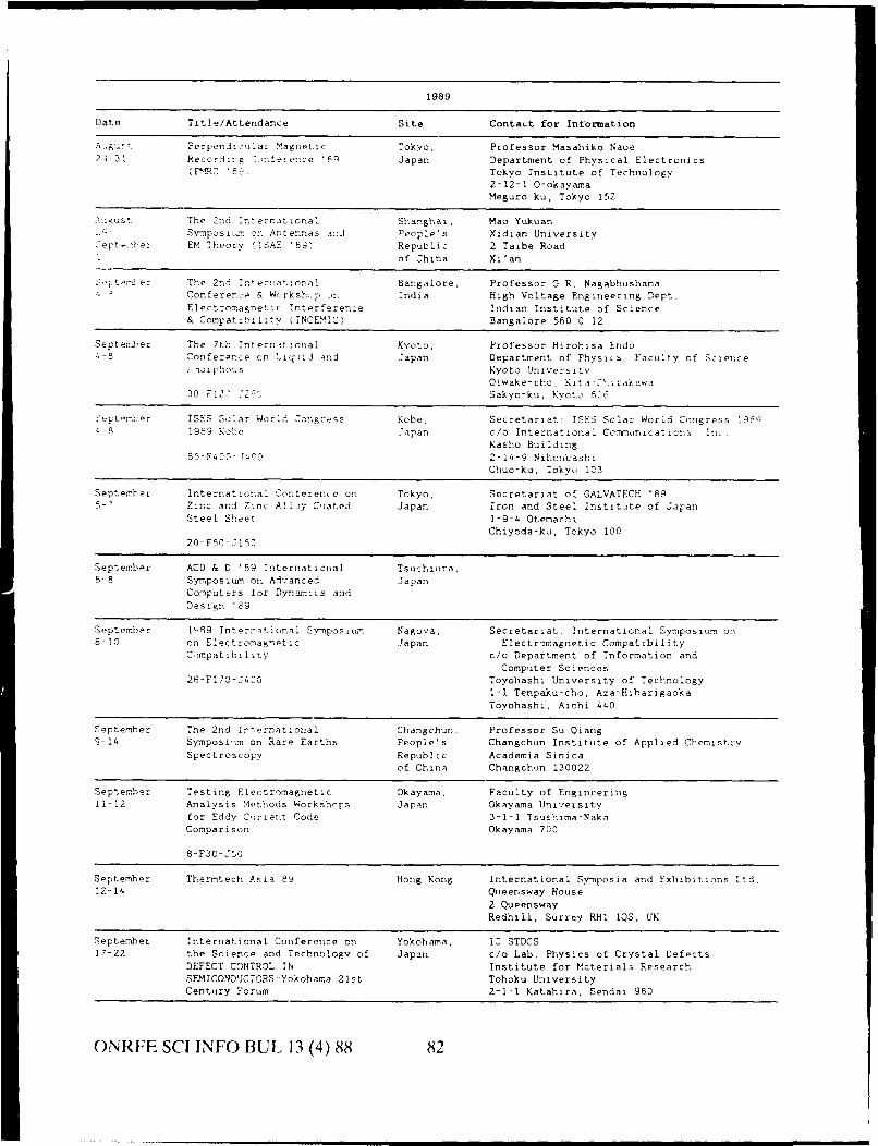
1989
Date Title/Attendance Site Contact for Information
A guct Perpenlicular Magnetic Tokyo, Professor Masahiko Naoe2?-31 Recorlirg 2.-.feence '8F Japan Department of Physical Electronics
(F-.C '89' Tokyo Institute of Technology2-12-1 0-okayamaMeguro-ku, Tokyo 152
A.1iust The 2nd international Shanghai, Mao YukuanSvmpos .or on Antennas a.o, People's Xidian University
e~toizer EM Theory ITSAE '89) Republic 2 Talbe Road
of China Xi'an
:,-t m' er The 2nd !nter attonal Bangalore. Professor G.R. NagabhushanaConference & Workshop on india High Voltage Engineering Dept.
Electromagnetic interference Indian Institute of Science& Compatsbil:ty (INCEMIC) Bangalore 560 0 12
Septembher The 7th Interndttmonal Kyoto, Professor Hirohisa EndoConference on Liqfiid and Japan Department of Physics, Faculty of Science'mcorphons Kyoto Universitv
Oiwake-cho. Kita . rakawa30-F12, -.'U Sakyo-ku, Kyoto 6C6
september ISES Solar World Congress Kobe, Secretariat: ISES Solar World Congress 19394-8 1989 Kohe Japan c/o International Communications, 'nc
Kasho Building65-F402- T400 2-14-9 Nihonbashi
Chuo-ku, Tokyo 103
September Internatlional Conference on Tokyo, Secretariat of GALVATECH '895-7 Zinc and Zinc Alloy Coated Japan Iron and Steel institute of JaFan
Steel Sheet. 1-9-4 OtemachiChiyoda-ku, Tokyo 100
20-FSC-J150
September ACD & D '89 international Tsuchiura,6-8 Sympos ium on Ad'anced Japan
Computers for Dynam..ics andDesign '89
September 1989 Inter:otionaL Symposium Nagoya, Secretariat. International Symposium on8-10 on Electromagnetic Japan Electromagnetic Compatibility
Compatibility c/o Department of Information andComputer Sciences
26-F170-J400 Toyohashi University of Technology1-1 Tenpaku-cho, Aza-Hibarigaoka
Toyohashi, Aichi 440
September The 2nd in.ternational Changchun. Professor Su Qiang9-14 Symposiim on Rare Earths People's Changchun Institute of Applied Chemistry
Spectroscopy Republic Academia Sinicaof China Changchun 130022
September Testing Electromagnetic Okayama, Faculty of Engineering11-12 Analysis Methods Worksho-s Japan Okayama University
for Eddy Cirtent Code 3-1-1 Tsushima-NakaComparison Okayama 700
8-F30-JSO
September Thermtech Asia 89 Hong Kong International Symposia and Exhibitions Ltd.12-14 Queensway House
2 Queensway
Redhill, Surrey RHI IQS, UK
September International Conference on Yokohama, I-STDCS17-22 the Science and Technology of Japan c/o Lab. Physics of Crystal Defects
DEFECT CONTROL IN Institute for Materialo ResearchSEMICONDUCTORS-Yokohama 21st Tohoku UniversityCentury Forum 2-1-1 Katahira, Sendai 980
ONRFE SCI INFO BUL 13 (4) 88 82

1989
Date Title/Attendance Site Contact for Information
September The 40th Meeting of Kyoto, Secretariat17-22 International Society of Japan 40th Meeting of International Society of
Electrochemistry Electrochemistryc/o Kyoto International Conference Hall
42-F200-J540 Takaragaike, Sakyo-ku, Kyoto 606
September The 3rd International Tokyo, Professor Tomoya Ogawa22-25 Symposium on Defect Japan Department t Physics
Recognition and Image Gakushuin UniversityProcessing for Research and Mejiro, Tokyo 171Development of Semiconductors(DRIP 1II)
September The 6th International Sapporo, Dr. Norio Satoh24-28 Symposium on Passivity - Japan Faculty of Engineering
Passivation of Metals and Hokkaido UniversitySemiconductors Nishi 8-chome, Kita 13-jo
Sapporo-shi 060
September The 5th International Hiroshima Faculty of Engineering25-28 Cunference on Numericai Ship (tentative) Hiroshima University
Hydrodynamics Shitami Saijo-choHigashi-Hiroshima 724
15-FS0-JI20
September The 16th International Karuizawa, Secretary: Professor T. Katoda25-29 Symposium on Gallium Arsenide Japan Research Center for Advanced Science and
and Related Compounds TechnologyUniversity of Tokyo4-6-1 KomabaMeguro-ku, Tokyo 153
September International Symposium on Kobe, Secretariat26-28 Optical Memory 1989 Japan c/o Business Center for Academic Societies
Japan3-23-1 HongoBunkyo-ku, Tokyo 113
October The 7th World Congress of the Sapporo, The 7th International Society for1-4 International Society for Japan Artificial Organs
Artificial Organs co International Communications Inc.Kasho Bldg
2-14-9 NihonbashiChuo-ku, Tokyo 103
October Today's Technology for the Kyoto, MMIJ/IMM Joint Symposium Office2-4 Mining and Metallurgical Japan Mining and Metallurgical Institute of
Industries JapanNogizaka Building
30-F300-J300 9-6-41 AkasakaMinato-ku, Tokyo 107
October MMIJ/IMM Joint Symposium Kyoto, Mining and Materials Processing Institute2-4 (Kyoto) Japan of Japan
Nogizaka Bldg30-F300-J3 0 9-6-41 Akasaka
Minato-ku, Tokyo 107
October The 3rd International Tokyo, Secretariat2-5 Conference on Computer Janan c/o Conference Department
Applications in Production and Business Center for Academic Societies JapanEngineering (CAPE 'P9) 3-23-1 Hongo
Bunkyo-ku, Tokyo 113
October The 10th Meeting of World Maehashi, De- rtment of Neurosurgery3-5 Society for Stereotart-c Japan Gumma University, School of Medicine
and Functional Neurosurgery 3-39 Showa-machiMaebashi 371
20-F20nj3-309
ONRIE SCI INFO BUL 13 (4) 88 83

1989
Date Title/Attendance Site Contact for Information
October The 9th International Display Kyoto, Secretariat of Japan Display '8915-18 Research Conference - Japan Japan c/o Japan Convention Services Inc.
Display '89 4F, Nippon Press Center Bldg2-2-1 Uchisaiwai-cho
27-F200-J500 Chiyoda-ku, Tokyo 100
October International Conference on Beijing, Continuing Education in Engineering22-26 Semiconductor and Integrated People's University Extension
Circuit Technology Republic University of Californiaof China 2223 Fulton Street
Berktley, CA 94720
October 1989 Joint Waste Management Kyoto,22-28 Conference 7apan
October International Conference on Tokyo,23-27 Coal Science Japan
October Electric Energy Conference Sydney, Conference Manager24-26 1989 Australia The Institution of Engineers, Australia
11 National Circuit
Barton, ACT 2600
October ACEAN Polymer Symposium Osaka, Institute of Scientific and Industrial26-28 Japan Res-arch, Osaka University
10-F30-J39 8-1 MihogaokaIbaraki-City, Osaka 567
November Aluminum and Magnesium Zhengzhou, Conference Office, !i6-10 People's 44 Portland Place
Republic London WIN 4BR, UKof China
November International Conference on Beijing, Secietariat of ICECM '897-10 Electronic Components and Fecpe'z c/o Professor Zhou Zhigang
Materials (ICECM '89) Republic Department of Chemical Engineeringof China Tsinghua University
Beijing 100084
November The 2nd International Singapore Secretariat7-10 Symposium. on the Physical IFFA Symposium
and Failure Analysis of Communication international AssociateIntegrated Circuits Pte Ltd.
450 Alexandra Road #10-00Inchcape House, Singapore 0511
November The 1989 International Kyoto, Professor Tsutomu Suzuki14-16 Symposium on Noise and Japan Department of Electronics
Clutter Rejection in Radar University of Electro-Communicationsand Imaging Sensors (ISNCR-89) Chofu-0,i, Tnkyo 182
November International Conference Kobe, International Conference Secretariat20-23 Evaluation of Materials Japan Conference and Editorial Department
Performance in Severe Iron and Steel Institute of JapanEnvironments-Evaluation and 1-9-4 OtemachiDevelopment of Materials in Chiyoda-ku, Tokyo 100Civil and Marine Uses
20-F80-T120
November The 1st International Symposium Makuhari, SAMPE20- and Exhibition of SAMPE Japan P.O. Box 2459December JAPAN CHAPTER Covina, CA 017221
ONRFE SCI INFO BUL 13 (4) 88 84

1989
Date Title/Attendance Site Contact for Information
November Tencon 89 Bombay, Kirit J. Sheth, Chairman22-24 India IEEE Bombay Section
c/o Hakotoronics Pvt. Ltd.Dadoji Konddeo Cross MargBombay 400 027, India
December The lCth Australasian Fluid Melbourne, 10AFMC11-15 Mechanics Conference Australia c/o Professor A.E. Peir,
Department of Mechanical EngineeringThe University of Melbourne
z-rkville, Victoria ?22
1990
Date Title/Attendance Site Contact for Information
January International Conference on Wollongong, Metallurgical Society of AIME22-26 Recrystallization in Metallic Australia Conference Department
Materials 420 Commonwealth DriveWarrendale, PA 15086
April 1993 International Topical Kobe, OC'90 Secretariat8-12 Meeting on Optical Computing Japan Business Center for Academic Societies
Japan (BCASJ)3-23-1 HongoBunkyo-ku. Tokyo 113
May The 27th International Osaka, Japan Organizing Committee for
19-26 Navigation Congress Japan 27th International Navigation Congressof PIANC
62-F500-JS00 c/o Port and Harbor Bureau
City of Osaka2-8-24 ChikkoMinato-ku, Osaka 552
July The 3rd International Kyoto, Professor Saichi Masaki1-6 Conference on T, hnology of Japan Department of Mechanical Engineering
Plasticity (3rd ICTP) Osaka Institute of Technology5-16-1 OmiyaAsahi-ku, Osaka 535
July The 10th International Tokyo, Japanese Society of Nephrology15-21 Congress of Nephiology Japan c/o 2nd Department of Internal Medicine
School of Medicine, Nippon University10-F1,000-J4,000 30-1 Oyaguchi-kamicho
Itabashi-ku, Tokyo 173
August International Congress -f Kyoto, ICM 90 Secretariat21-29 Mathematicians 1990 Japan c/o International Relations Office
Research Institute for Mathematical Sciences84-FI,500-JI.500 Kyoto University
Kitashirakawa Oiwake-cho
Sakyo-ku, Kyoto 606
August V Internatinnal Congress Yokohama, Secretary General's Office for INTECOL 199023-30 of Ecology Japan c/o Institute of Environmental Science and
Technology62-F900-J1,000 Yokohama National University
156 TokiwadaiHodogaya-ku, Yokohama 240
September IUMS Congress Bacteriology Osaka, Preliminary Committee of International16-22 and Mycology - Osaka, Tapan - Japan Congress of Microbiology
1990 c/o JTB Creative Inc.
Daiko Building71-F2.,0C- ,70 3-2-14 Umeda
Kita-ku, Osaka 530
ONRFE SCI INFO B13IL 13 (4) 88 85

1990
Date Title/Attendance Site Contact for Information
September The 6th International Congress Shanghai, ICPIC-90 Secretariat24-27 on Polymers in Concrete People's c/o Associate Professor Tan Muhua
Republic Institute of Materials Science andof China Engineering
Tongji UniversityShanghai
September The 15th International Osaka, Preliminary Committee of International,tentative) Congress on Microbiology Japan Congress of Microbiology
c/o JTB Creative Inc.57-F2,5C0-J2,5C0 Daiko Building
3-2-14 UmedaKita-ku, Osaka 530
October The 4th International Kobe, The Marine Engineering Society in Japan15-19 Symposium on Marine Japan Hibiya Osaka 2nd Bldg
Engineering (ISME KOBE '90) 1-2-2 Uchisaiwai-cho
Chiyoda-ku, Tokyo 100
October The 6th International Nagoya, International Cc.iference Department21-26 Iron and Steel Congress Japan Iron and Steel Institute of Japan
3F, Keidanren Kaikan50-F3C0-j500 1-9-4 Otemachi
Chiyoda-ku, Tokyo 100
1990 Chemeca 1990 Applied New Zealand Conference Manager(tentative) Thermodynamics The Institution of Engineers, Australia
11 National Circuit
Barton, ACT 2600
1991
Date Title/Attendance Site Contact for Information
February POLYMER '91: International Melbourne, Dr. G.B. Guise10-15 Symposium on Polymer Australia P.O. Box 224
Materials Belmont, VIC 3216, Australia
August International Congress on Kyoto, National Institute of Radiological Science(tentative) Medical Physics Japan 4-9-1 Anagawa
Chiba 26045-F600-J900
August The 16th International Kyoto, Japan Society of Medical Electronics and(tentative) Conference on Medical and Japan Biological Engineering
Biological Engineering (tentative) 2-4-16 Yoyogi(ICMBE) Bunkyo-ku, Tokyo 113
1992
Date Title/Attendance Site Contact for Information
October The 14th International Yokohama, NTT Communication Switching Laboratories26-30 Switching Symposium (ISS '92) Japan 3-9-11 Midori-cho
Musashino-shi, Tokyo 18060-FI,200-J800
Autumn XIVth International Switching (to be Institute of Electronics, Information andSymposium (ISS '92) decided) Communication Engineers (IEICE)
Kikai Shinko Kaikan5-5-8 Shiba-koenMinato-ku. Tokyo 105
ONRFE SCI INFO BUL 13 (4) 88 86

1993
Date Title/Attendance Site Contact for Information
1993 International Federation of Sydney, Conference Manager(tentative) Automatic Control Congress Australia The Institution of Engineers, Australia
11 National CircuitBarton, ACT 2600
1994
Date Title/Attendance Site Contact for Information
Tentative XO( International Conference Kyoto, Professor Hitoshi Ohtakion Coordination Chemistry Japan Coordination Chemistry Laboratories
Institute for Molecular ScienceMyodaiji-cho, Okazaki 444
ONRFE SCI INFO BUL 13 (4) 88 87

SCIENTIFIC INFORMATION BULLETININDEX, VOLUME 13
AUTHORS SUBJECTS (continued)
B ottka, N . .......................................................... 3-031 C alcium ionophorcs .......................................... 3-0 28Broussard, Phillip R ......................................... 4-001 C eram ic superlattices ........................................ 3-018Burt, Wayne V ............................. 1-016, 1-067, 4-039 Chalcopyrite semiconductor ............................ 2-007Callen, Earl 1-001, 1-051, 3-001, 3-061, 4-001, 4-013 Chemical vapor deposition .............................. 4-026Cutler, Robert S ............................................... 2-1)17 Chcvrel phase com pounds ................................ 2-070Eagar, Thomas W ..................... 1-019 CO 2 lasers ............................................................ 1-019Falco, Charles M ............................................... 4-031 Computational fluid dynamics ..................... 4-061Fuller, W endy .................................................... 2-083 C om puter m odeling .......................................... 2-077G askill, D .K ....................................................... 3-031 C om puter system s .............................................. 3-053K aw ano, Sandy .................................................. 2-0W 1 C onstitutive relations ........................................ 1-035K usam ichi, H idctakc ........................................ 3-039 C ritical current density ...................................... 1-0 )30Lenoe, Edward M ark ........................................ 2-033 Critical field m easurem ent ................................ 2-085M ajde, Jeannine A ............................... 3-027, 3-071 Critical m agnetic field ...................................... 3-003M etzbower, EA . .............................................. 4-069 C rystalline 1-2-3 structure ................................ 1-043M itchell, D ean L ............................................... 2-065 C ytokine research .............................................. 3-072M olnar, D aniel 0 ............................................. 2-077 dc field facilities and research .......................... 2-067O sofsky, M ichael .............................................. 4-001 D iam ond sem iconductor .................................. 2-006Pettit, Fred ........................................................ 4-025 D im ensional crossover ...................................... 3-013Sasada, Ichiro .................................................... 3-06 1 D oping .................................................... 3-034, 4-045Schuller, Ivan K .................. 1-042, 3-001 Domain walls ........................ 1-003T achiki, M asashi ................................................ 3-00 1 E icosenoids ........................................................ 3-029T esche, C laudia D ............................................. 1-037 E lectrical current ................................................ 1-035T irrell, D avid A ................................................. 1-047 E lectron holography .......................................... 1-007U shino, Yuko ...... 1-051, 1-077, 2-093, 3-075, 4-075 Endotoxin ............................................................ 3-027Wright, George B ....................... 1-024, 1-073, 2-005 Endotoxin measurement methods .................. 3-029Yoshihara, H ......................................... 3-053, 4-061 Energy bandgap ............................................. 2-010
E pitaxial growth ................................................ 2-009Exchange energy ................................................ 1-003
SUBJECTS Faraday effect .................................................... 1-007Ferromagnetic domains .................................... 1-001
Acceptors..........................2-007 Fifth generation computer system .................. 3-053
Air-sea interaction ............................................ 4-042 Films..............................2-084Antiferromagnetic state ................................. Film growth
A rtificial intelligence ........................................ 2-077 By evaporation ............................................ 4-002
A rtificial structures ........ ............................. 2-089 By sputtering .............................................. 4-003
A ustralia ............................................................ 1-047Band theory ........................................................ 4-047 Pinning .. .............................................. 1-033Bidirectional communication between F uantization ........................................... 1-027
brain and immune system ........................ 3-072 Fuzzy Set theory. ...................................... 2-080Biomagnetism...................................... 1-037 Gspesr itrn.........-3Biom aterials .................................................... 4-071 G inzburg-Landau theory ...................... 1-027, 3-004Bio nat ria s ........................................ 4- 71G rowth m echanism s .......................................... 3-035B itter patterns .................................................... 1-007B loch w alls ........................................................ 1-005
ONRFE SCI INFO BUL 13 (4) 88 89

SUBJECTS (continued) SUBJECTS (continued)
Heavy fermions .................................................. 2-089 Monsoon research .............................................. 1-068Heterojunction bipolar transistors .................. 3-033 Mott transition .................................................... 4-051High electron mobility transistors .................. 3-031 Muramyl dipeptide in the brain ...................... 3-071High temperature Near-surface sound transmission .................... 1-017
superconductivity ........ 1-042, 1-051, 2-083 Ndel walls ............................................................ 1-005Hot isostatic pressing seminar ........................ 2-059 Neuroendocrine modulation ............................ 3-071Hot isostatic pressing technology .................... 2-033 Neuroleukin ........................................................ 3-072Hot pressing ceramics ...................................... 2-036 Neuromagnetism ................................................ 1-039Hubbard model ................................................ 4-050 Neutron scattering .................... 4-045Immunopharmacology ...................................... 3-071 Oceanography ............................ 1-016, 1-067, 4-039India ........................................................ 1-016, 1-067 O ptoelectronic devices ...................................... 2-005Industrial research ............................................ 2-017 Organic superconductors .................................. 2-087Interface energy ................................................ 1-031 O xide ceram ics .................................................. 1-042Japan .............................. 1-001, 1-019, 1-051, 1-073, Oxide superconductors ...................................... 2-089
2-001, 2-005, 2-017, 2-033, Oxygen planes versus chains ............................ 2-0852-065, 2-077, 2-083, 3-023, People's Republic of China .............................. 3-0393-027, 3-031, 3-053, 3-071, Photophysical probes of structure .................... 1-0484-001, 4-025, 4-031, 4-039, Polymeric resist materials ................................ 1-049
4-061, 4-069 Powder metallurgy ............................................ 3-044Japanese government ...................................... 1-051 Private sector superconductivity research ...... 1-060Japanese ministries .......................................... 1-051 Production of titanium mill products .............. 3-041Japanese "old-boy" network ............. 2-027 Proximity effect ...................... 1-045Japanese writing system ................ 1-073 Pulsed-field facilities & research .......... 2-068Japan Prize ........................................................ 2-001 R & D m anagem ent ............................................ 2-028K anji .................................................................... 1-073 R adiation chem istry .......................................... 1-04 7Kerr effect .......................................................... 1-007 R adiation-resistant m aterials ............................ 1-049Knowledge information processing system .... 3-053 Recovery/recycling of titanium scrap .............. 3-041Kuroshio Current research .............................. 4-039 Rectangular shaping of laser beams ................ 1-019Laser processing ................................................ 1-019 Reflection Lorentz microscopy ........................ 1-008Lattice constant ................................................ 2-010 Remanent magnetic fields ................................ 1-040London current equation ................................ 1-025 Salinity distribution ............................................ 1-017Lorentz microscopy .......................................... 1-007 Science and technology award .......................... 2-001Macroscopic properties .................................... 1-024 Secondary electrons .......................................... 1-008Magnetic domains ............................................ 1-001 Self-compensation ........................................ 2-008Magnetic shaking .............................................. 3-066 Semiconductors ...................................... 2-005, 3-031Magnetic shielding ............................................ 3-063 Sequential logic programming language ........ 3-056M agnetic transport ............................................ i-044 Shallow donors .................................................. 2-007M agnetism .......................................................... 2-086 Shielding by a spherical shell ............................ 3-064Magnetite .......................................................... 4-052 Silicon carbide ....................... 2-046Magnetocardiology .......................................... 1-039 Silicon carbide coatings research .................... 4-025Magnetocrystalline anisotropy ........................ 1-003 Silicon nitride ...................................................... 2-037M agnetostatics .................................................. 1-001 Single crystal film s .............................................. 4-014Mangrove reforestation .................................... 1-069 Single crystal measurements ........................... 2-084Maxwell's equations .......................................... 1-035 Singular value decomposition .......................... 2-079Mechanisms of reactions .................................. 1-048 Spin-polarized scanning electron microscope 1-008Megagauss magnetic field research .............. 2-065 SQUID magnetometer systems ...................... 1-037M eissner effect .................................................. 1-025 Substitution ....................................................... 2-085Metallic multilayers .............................. 4-032, 4-070 Supercomputers ...................................... 4-061, 4-072Metallic superlattices ............................ 4-032, 4-070 Superconducting properties ......................... 4-011Metal-organic vapor phase epitaxy ................ 3-031 Superconducting synchrotron .......................... 4-036
ONRFE SCI INFO BUL 13 (4) 88 90

SUBJECTS (continued) RESEARCH FACILITIES/
Superconducting thin films .................. 4-001, 4-034 INSTITUTIONS (continued)Superconductivity .......... 1-024, 3-001, 3-063, 4-001, Ministry of Posts and Telecommunications .... 1-056
4-031, 4-043 Ministry of Transport ........................................ 1-056Superconductivity budgets .............................. 1-056 Mitsubishi Electric Company .......................... 1-020Superlattices ...................................................... 3-001 National Institute of Oceanography ................ 1-067Surface waves in ocean .................................... 1-016 National Research Institute for Metals,Technology transfer survey .............................. 2-017 Tsukuba Laboratories ................................ 4-016Technology transfer techniques ...................... 4-025 National Science Foundation ............................ 3-023Ternary superconductors ................................ 2-088 Naval Physical and OceanographicalT hin film s .......................................................... 2-087 Laboratory .................................................. 1-016Thom as-Ferm i screening ................................ 4-051 N EC Corp ........................................................... 4-034T itanium ............................................................ 3-039 O saka U niversity .................................... 2-070, 4-018Titanium Osaka University Welding Research
A lloys .......................................................... 3-04 1 Institute ........................................................ 1-0 19Applications ................................................ 3-045 Research Institute for Metal Surface ofMelting and casting .................................. 3-040 High Performance (RIMES) .................... 4-025Sponge ........................................................ 3-048 Science and Technology Agency ...................... 1-051
T oxicity .............................................................. 3-027 Sum itom o E lectric Industries .......................... 4-017Transmission electron microscopy .................. 1-007 Sumitomo Heavy Industries .............................. 4-036University research .......................................... 2-017 Tokyo Institute of Tcchnology ......................... 2-005U pper critical field ............................................ 3-005 U niversity of T okyo .......................................... 4-035V ortex m otion .................................................... 1-033V ortices ............................................................. 3-009Water temperaturc distribution ...................... 1-017 LOCATIONSWhisker reinforcement .................................... 2-050Zincblende semiconductor .............................. 2-007 AustraliaZ irconia ceram ics .............................................. 2-049
N o o sa .......................................................... 1-04 7
RESEARCH FACILITIES/ India
INSTITUTIONSC o ch in .......................................................... 1-0 16
Canon Central Research Laboratory ............ 4-033 G oa .............................................................. 1-067
Electrical CommunicationsLaboratory, NTT ..................................... 4-015 Japan
Electrotechnical Laboratory ............................ 4-016ICOT Research Center ................................... 3-054 Atsugi..........................4-033Institute of Solid State Physics ........... 2-071 lbaraki ......................... 4-015
Institute for Chem ical Research, Itam i City .................................................... 4-017
K yoto U niversity . .................................... 4-014 K aw asaki ...................................................... 4-034Japan Research and Development Kvoto ............................................................ 4-014
Center for Metals ......................... 4-026, 4-033 (),,ka ........... 1-019, 2-070, 4-0l1.1, 4-019
M atsushita Electric Industrial Co., Ltd ......... 4-019 T.nashi City ................................................ 4-030
M inistry of Education ...................................... 1-056 Tokyo ........................ 1-037, 2-(X)5, 2-071, 3-054
M inistry of International T rade T ,O:uba ........................................................ 4-016
and Industry ................................................ 1-055
ONRFE SCI INFO BUL 13 (4) 88 91OU. S.COVERNMENT PRINTING wFr ICE,:!19.-241-59 :91902

NOTICE
The Office of Naval Research/Air Force Office of Scientific Research/ArmyResearch Office, Liaison Office, Far East is located on the second floor of Bldg#1, Akasaka Press Center and bears the following mail identification:
Mailing address: Office of Naval Reseach/Air ForceOffice of Scientific Research/ArmyResearch Office
Liaison Office, Far EastAPO San Francisco 96503-0007
Local address: ONR/AFOSR/ARO Far EastAkasaka Press Center7-23-17, RoppongiMinato-ku, Tokyo 106
Telephone numbers: Civilian 03-401-8924Autovon 229-3236Telefax 03-403-9670
1NO POSTAGEOi-r-ICIAL BUSINESS NIECESSARY
PENALTY FOR PRIVATE USE, 300 IF MAILED
IN THEUNITED STATES
BUSINESS REPLY MAILFIRST CLASS PERMIT NO. 12503 WASH., D C.
POSTAGE WILL BE PAID BY DEPARTMENT OF THE NAVY
OFFICE OF NAVAL RESEARCHLIAISON OFFICE, FAR EASTAPO SAN FRANCISCO 96503-0007