Embed Size (px)
Citation preview

APPLICATION NOTE
REJ05B0735-0100 September 2005 Page 1 of 15
SH7080 Group SCIF Asynchronous Serial Data Transmission Function
Introduction This application note describes the serial data transmission function that uses the transmit-FIFO-data-empty interrupt source of the SCIF (Serial Communication Interface with FIFO). You can use this application note as reference information for designing user software.
Target Device SH7085 (R5F7085)
Contents
1. Specifications .................................................................................................................................... 2
2. Operational Overview of Functions Used ......................................................................................... 3
3. Principles of Operation...................................................................................................................... 5
4. Description of Software..................................................................................................................... 7
5. Flowcharts....................................................................................................................................... 12
SH7080 Group SCIF Asynchronous Serial Data Transmission Function
REJ05B0735-0100 September 2005 Page 2 of 15
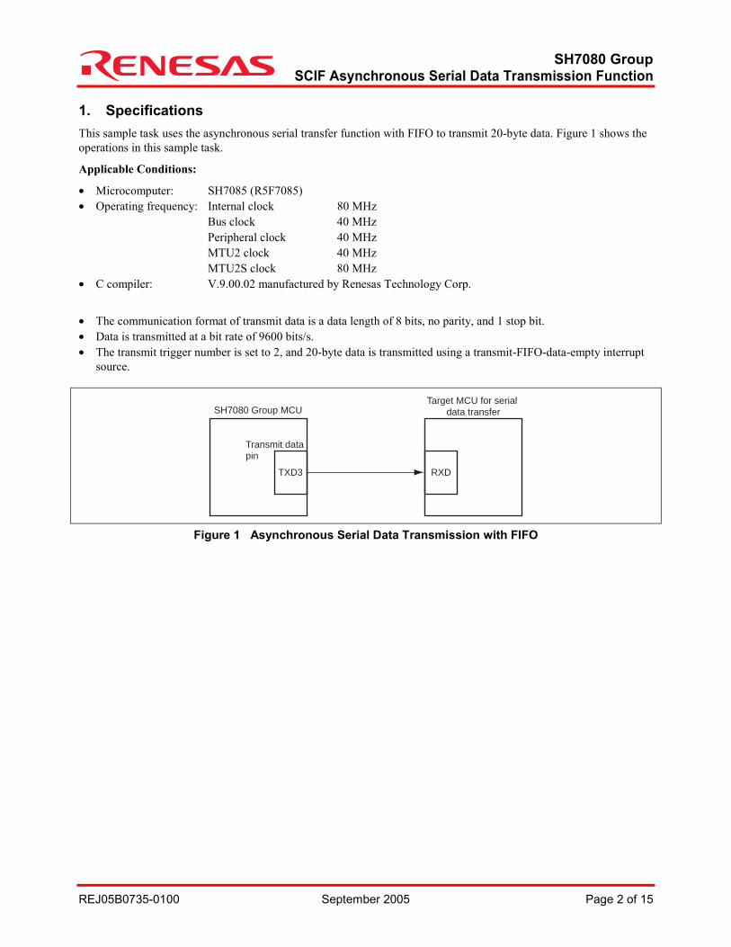
1. Specifications This sample task uses the asynchronous serial transfer function with FIFO to transmit 20-byte data. Figure 1 shows the operations in this sample task.
Applicable Conditions:
• Microcomputer: SH7085 (R5F7085) • Operating frequency: Internal clock 80 MHz
Bus clock 40 MHz Peripheral clock 40 MHz MTU2 clock 40 MHz MTU2S clock 80 MHz
• C compiler: V.9.00.02 manufactured by Renesas Technology Corp.
• The communication format of transmit data is a data length of 8 bits, no parity, and 1 stop bit. • Data is transmitted at a bit rate of 9600 bits/s. • The transmit trigger number is set to 2, and 20-byte data is transmitted using a transmit-FIFO-data-empty interrupt
source.
TXD3
SH7080 Group MCU
Transmit data
pin
RXD
Target MCU for serial
data transfer
Figure 1 Asynchronous Serial Data Transmission with FIFO
SH7080 Group SCIF Asynchronous Serial Data Transmission Function
REJ05B0735-0100 September 2005 Page 3 of 15
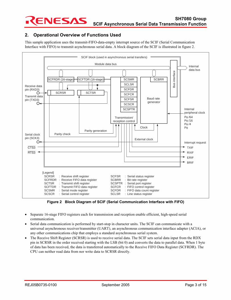
2. Operational Overview of Functions Used This sample application uses the transmit-FIFO-data-empty interrupt source of the SCIF (Serial Communication Interface with FIFO) to transmit asynchronous serial data. A block diagram of the SCIF is illustrated in figure 2.
SCFRDR (16-stage) SCFTDR (16-stage) SCSMR
SCLSR
SCFDR
SCFCR
SCFSR
SCSCR
SCSPTR
Transmission/
reception control
Parity generation
External clock
Parity check
SCRSR
Receive data
pin (RXD3)
Transmit data
pin (TXD3)
Serial clock
pin (SCK3)
RXIF
TXIF
[Legend]
SCRSR : Receive shift register
SCFRDR : Receive FIFO data register
SCTSR : Transmit shift register
SCFTDR : Transmit FIFO data register
SCSMR : Serial mode register
SCSCR : Serial control register
SCFSR : Serial status register
SCBRR : Bit rate register
SCSPTR : Serial port register
SCFCR : FIFO control register
SCFDR : FIFO data count register
SCLSR : Line status register
Internal
peripheral clock
Pφ /64
Pφ /16
Pφ /4Pφ
Interrupt request
ERIF
BRIF
CTS3
RTS3
SCTSR
SCBRR
Baud rate
generator
Bu
s in
terf
ace
Module data busInternal
data bus
Clock
SCIF block (used in asynchronous serial transfers)
Figure 2 Block Diagram of SCIF (Serial Communication Interface with FIFO)
• Separate 16-stage FIFO registers each for transmission and reception enable efficient, high-speed serial
communication. • Serial data communication is performed by start-stop in character units. The SCIF can communicate with a
universal asynchronous receiver/transmitter (UART), an asynchronous communication interface adapter (ACIA), or any other communications chip that employs a standard asynchronous serial system.
• The Receive Shift Register (SCRSR) is used to receive serial data. The SCIF sets serial data input from the RDX pin in SCRSR in the order received starting with the LSB (bit 0) and converts the data to parallel data. When 1 byte of data has been received, the data is transferred automatically to the Receive FIFO Data Register (SCFRDR). The CPU can neither read data from nor write data to SCRSR directly.

SH7080 Group SCIF Asynchronous Serial Data Transmission Function
REJ05B0735-0100 September 2005 Page 4 of 15
• The Receive FIFO Data Register (SCFRDR) is a 16-stage FIFO register (each stage is 8 bits) used to hold received serial data. When 1 byte of serial data has been received, the received serial data is transferred from the Receive Shift Register (SCRSR) to SCFRDR for storage, completing the receive operation. Receive operations can be performed successively until 16 bytes of data are stored in the register. The CPU can read data from SCFRDR, but it cannot write data to SCFRDR. If a read from the Receive FIFO Data Register is attempted when there is no receive data in the register, the value read is undefined. When the register has become full with receive data, any subsequently received serial data is lost.
• The Transmit Shift Register (SCTSR) is used to transmit serial data. The SCIF transfers transmit data from the Transmit FIFO Data Register (SCFTDR) to SCTSR, and then performs serial data transmission by sending the data to the TXD pin in order starting with the LSB (bit 0). When 1 byte of data has been transmitted, the next transmit data is transferred automatically from SCFTDR to SCTSR to start transmission. The CPU can neither read data from nor write data to SCTSR directly.
• The Transmit FIFO Data Register (SCFTDR) is a 16-stage FIFO register (each stage is 8 bits) used to hold data that is to be transmitted serially. When the SCIF detects that the Transmit Shift Register (SCTSR) is empty, the SCIF starts serial transmission by transferring the transmit data written in SCFTDR to SCTSR. Serial transmission can be performed as long as data remains in SCFTDR. The CPU can write data to SCFTDR at any time. When SCFTDR becomes full with transmit data (16 bytes), no more data can be written. If an attempt is made to write more data, the data is ignored.
• The Serial Mode Register (SCSMR) is a 16-bit register used to set the SCIF serial communication format and select the clock source of the baud rate generator. The CPU can read data from and write data to SCSMR at any time.
• The Serial Control Register (SCSCR) is a 16-bit register used to enable or disable SCIF transmit and receive operations and interrupt requests, and to select the transmit/receive clock source. The CPU can read data from and write data to SCSCR at any time.
• The Serial Status Register (SCFSR) is a 16-bit register. The upper 8 bits indicate the number of receive errors in the data in the Receive FIFO Data Register, and the lower 8 bits consist of status flags indicating the SCIF operating state. The CPU can read data from and write data to SCFSR at any time. However, 1 cannot be written in the ER, TEND, TDFE, BRK, RDF, and DR status flags. Before these flags can be cleared to 0, they must first be read as 1. The FER and PER flags are read-only flags, and data cannot be written to them.
• The Bit Rate Register (SCBRR) is an 8-bit register that sets the serial transmit/receive bit rate together with the baud rate generator clock source selected by the CKS1 and CKS0 bits of the Serial Mode Register (SCSMR). The CPU can read data from and write data to SCBRR at any time. SCBRR is initialized to H'FF by a power-on reset.
• The FIFO Control Register (SCFCR) is a 16-bit register used to reset the number of data and set the trigger data number for the Transmit FIFO Data Register and the Receive FIFO Data Register. The register also contains a loopback test enable bit. The CPU can read data from and write data to SCFCR at any time.
• The FIFO Data Count Register (SCFDR) is a 16-bit register that indicates the number of data bytes stored in the Transmit FIFO Data Register (SCFTDR) and in the Receive FIFO Data Register (SCFRDR). The upper 8 bits indicate the number of transmit data bytes in SCFTDR, and the lower 8 bits indicate the number of receive data bytes in SCFRDR. The CPU can read data from SCFDR at any time.
• The Line Status Register (SCLSR) is a 16-bit register that the CPU can read from and write to at any time. However, 1 cannot be written to the ORER status flag. Before the ORER status flag can be cleared to 0, it must first be read as 1.
SH7080 Group SCIF Asynchronous Serial Data Transmission Function
REJ05B0735-0100 September 2005 Page 5 of 15
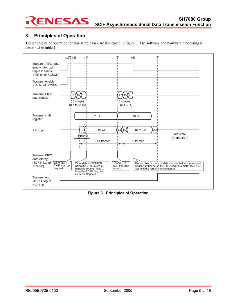
3. Principles of Operation The principles of operation for this sample task are illustrated in figure 3. The software and hardware processing is described in table 1.
Transmit-FIFO-data-
empty interrupt
request enable
(TIE bit of SCSCR)
Transmit enable
(TE bit of SCSCR)
Transmit FIFO
data register
Transmit shift
register
TXD3 pin
Transmit FIFO
data empty
(TDFE flag of
SCFSR)
Transmit end
(TEND flag of
SCFSR)
Idle state
(mark state)1 frame
14 frames 6 frames
1 to 16
1 to 14 15 to 20
17 to 20
1 2 to 13 14 15 18 to 19 20
(1)(2)(3) (4) (5) (6) (7)
Generate a TXIF interrupt request
Write data to SCFTDR using the TXIF interrupt handling routine, read 1 from the TDFE flag, and clear the flag to 0
The number of transmit data items is below the transmittrigger number set in the FIFO control register (SCFCR) (set with the remaining two bytes)
16 stages
(8 bits × 16)
4 stages
(8 bits × 4)
Generate a TXIF interrupt request
Figure 3 Principles of Operation
SH7080 Group SCIF Asynchronous Serial Data Transmission Function
REJ05B0735-0100 September 2005 Page 6 of 15
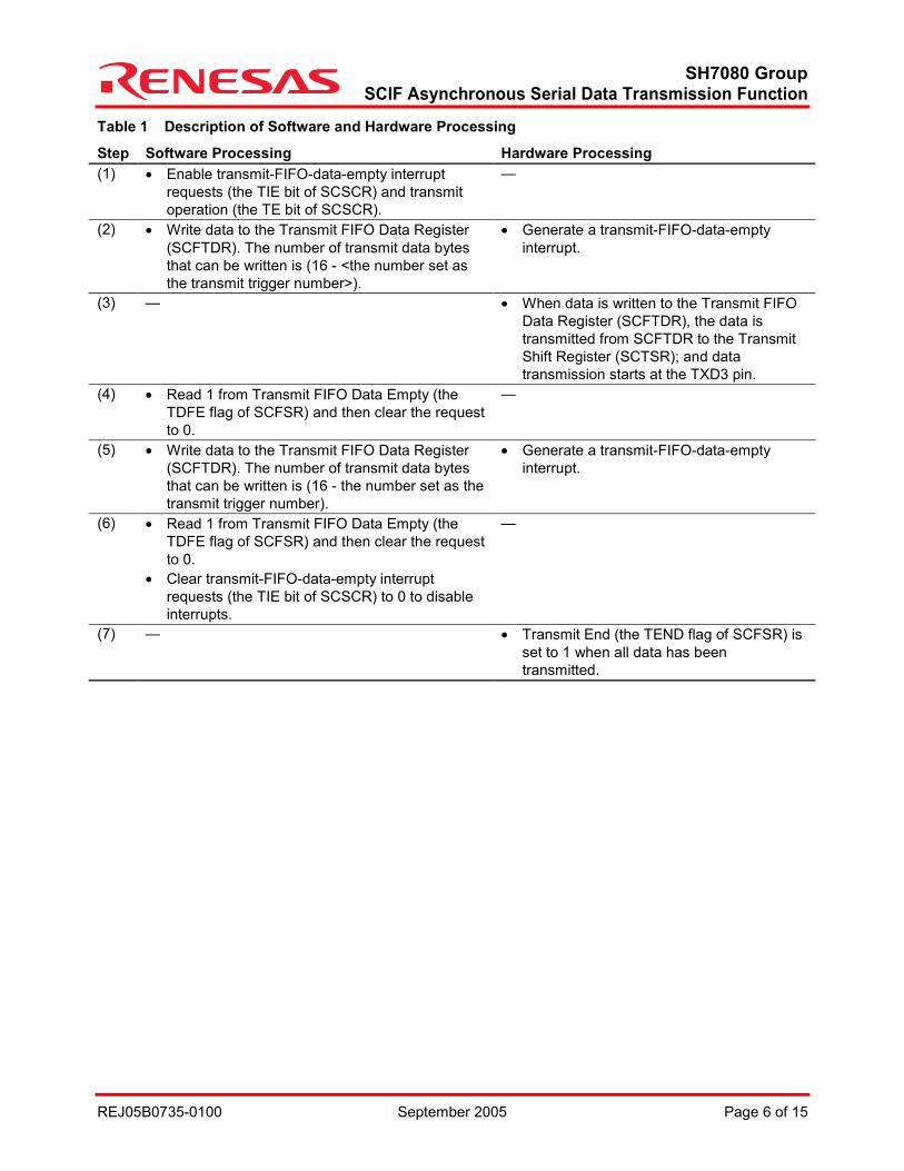
Table 1 Description of Software and Hardware Processing
Step Software Processing Hardware Processing (1) • Enable transmit-FIFO-data-empty interrupt
requests (the TIE bit of SCSCR) and transmit operation (the TE bit of SCSCR).
—
(2) • Write data to the Transmit FIFO Data Register (SCFTDR). The number of transmit data bytes that can be written is (16 - <the number set as the transmit trigger number>).
• Generate a transmit-FIFO-data-empty interrupt.
(3) — • When data is written to the Transmit FIFO Data Register (SCFTDR), the data is transmitted from SCFTDR to the Transmit Shift Register (SCTSR); and data transmission starts at the TXD3 pin.
(4) • Read 1 from Transmit FIFO Data Empty (the TDFE flag of SCFSR) and then clear the request to 0.
—
(5) • Write data to the Transmit FIFO Data Register (SCFTDR). The number of transmit data bytes that can be written is (16 - the number set as the transmit trigger number).
• Generate a transmit-FIFO-data-empty interrupt.
(6) • Read 1 from Transmit FIFO Data Empty (the TDFE flag of SCFSR) and then clear the request to 0.
• Clear transmit-FIFO-data-empty interrupt requests (the TIE bit of SCSCR) to 0 to disable interrupts.
—
(7) — • Transmit End (the TEND flag of SCFSR) is set to 1 when all data has been transmitted.
SH7080 Group SCIF Asynchronous Serial Data Transmission Function
REJ05B0735-0100 September 2005 Page 7 of 15
4. Description of Software
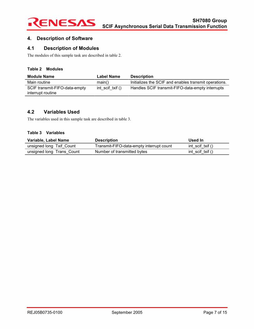
4.1 Description of Modules The modules of this sample task are described in table 2.
Table 2 Modules
Module Name Label Name Description Main routine main() Initializes the SCIF and enables transmit operations. SCIF transmit-FIFO-data-empty interrupt routine
int_scif_txif () Handles SCIF transmit-FIFO-data-empty interrupts
4.2 Variables Used The variables used in this sample task are described in table 3.
Table 3 Variables
Variable, Label Name Description Used In unsigned long Txif_Count Transmit-FIFO-data-empty interrupt count int_scif_txif () unsigned long Trans_Count Number of transmitted bytes int_scif_txif ()
SH7080 Group SCIF Asynchronous Serial Data Transmission Function
REJ05B0735-0100 September 2005 Page 8 of 15
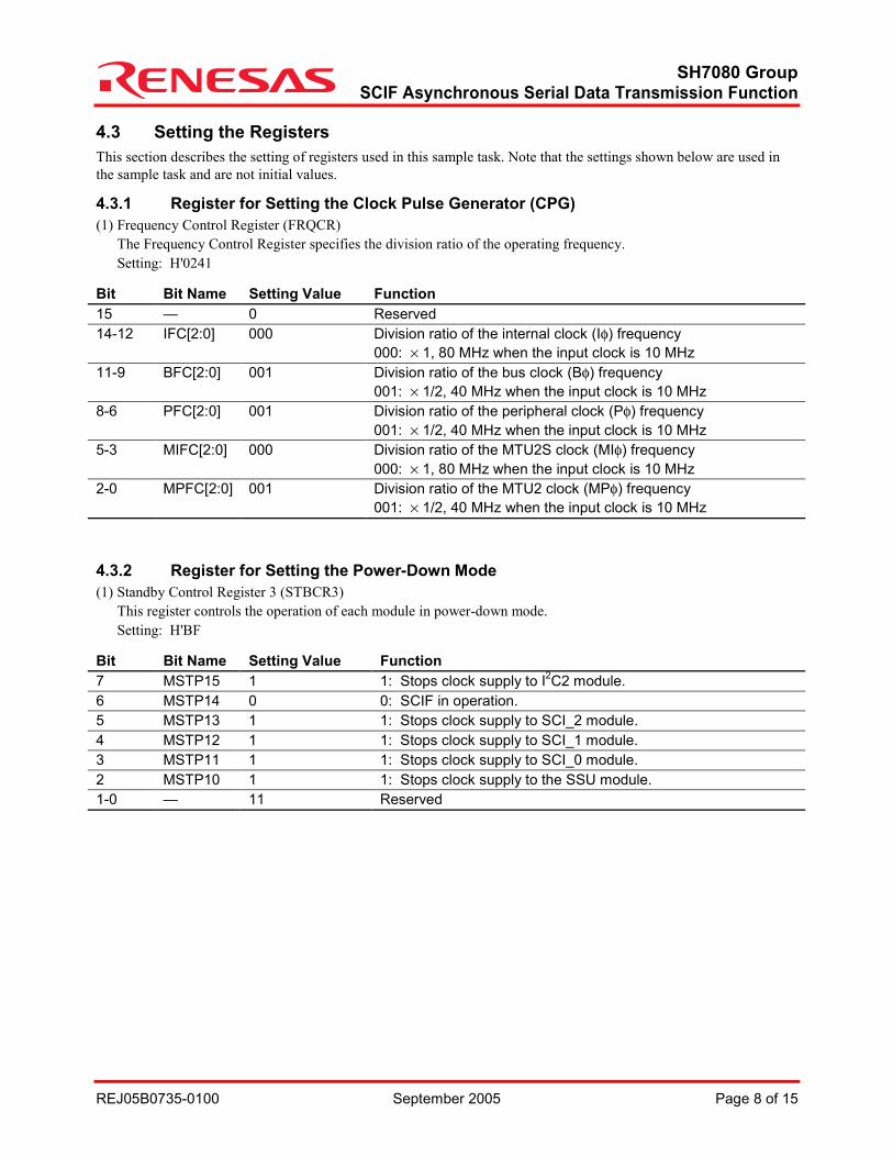
4.3 Setting the Registers This section describes the setting of registers used in this sample task. Note that the settings shown below are used in the sample task and are not initial values.
4.3.1 Register for Setting the Clock Pulse Generator (CPG) (1) Frequency Control Register (FRQCR)
The Frequency Control Register specifies the division ratio of the operating frequency. Setting: H'0241
Bit Bit Name Setting Value Function 15 — 0 Reserved 14-12 IFC[2:0] 000 Division ratio of the internal clock (Iφ) frequency
000: × 1, 80 MHz when the input clock is 10 MHz 11-9 BFC[2:0] 001 Division ratio of the bus clock (Bφ) frequency
001: × 1/2, 40 MHz when the input clock is 10 MHz 8-6 PFC[2:0] 001 Division ratio of the peripheral clock (Pφ) frequency
001: × 1/2, 40 MHz when the input clock is 10 MHz 5-3 MIFC[2:0] 000 Division ratio of the MTU2S clock (MIφ) frequency
000: × 1, 80 MHz when the input clock is 10 MHz 2-0 MPFC[2:0] 001 Division ratio of the MTU2 clock (MPφ) frequency
001: × 1/2, 40 MHz when the input clock is 10 MHz
4.3.2 Register for Setting the Power-Down Mode (1) Standby Control Register 3 (STBCR3)
This register controls the operation of each module in power-down mode. Setting: H'BF
Bit Bit Name Setting Value Function 7 MSTP15 1 1: Stops clock supply to I2C2 module. 6 MSTP14 0 0: SCIF in operation. 5 MSTP13 1 1: Stops clock supply to SCI_2 module. 4 MSTP12 1 1: Stops clock supply to SCI_1 module. 3 MSTP11 1 1: Stops clock supply to SCI_0 module. 2 MSTP10 1 1: Stops clock supply to the SSU module. 1-0 — 11 Reserved
SH7080 Group SCIF Asynchronous Serial Data Transmission Function
REJ05B0735-0100 September 2005 Page 9 of 15
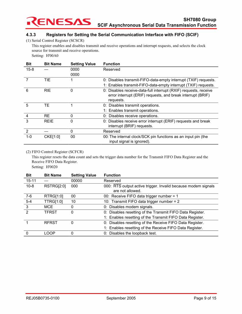
4.3.3 Registers for Setting the Serial Communication Interface with FIFO (SCIF) (1) Serial Control Register (SCSCR)
This register enables and disables transmit and receive operations and interrupt requests, and selects the clock source for transmit and receive operations. Setting: H'00A0
Bit Bit Name Setting Value Function 15-8 — 0000
0000 Reserved
7 TIE 1 0: Disables transmit-FIFO-data-empty interrupt (TXIF) requests. 1: Enables transmit-FIFO-data-empty interrupt (TXIF) requests.
6 RIE 0 0: Disables receive-data-full interrupt (RXIF) requests, receive error interrupt (ERIF) requests, and break interrupt (BRIF) requests.
5 TE 1 0: Disables transmit operations. 1: Enables transmit operations.
4 RE 0 0: Disables receive operations. 3 REIE 0 0: Disables receive error interrupt (ERIF) requests and break
interrupt (BRIF) requests. 2 — 0 Reserved 1-0 CKE[1:0] 00 00: The internal clock/SCK pin functions as an input pin (the
input signal is ignored). (2) FIFO Control Register (SCFCR)
This register resets the data count and sets the trigger data number for the Transmit FIFO Data Register and the Receive FIFO Data Register. Setting: H'0020
Bit Bit Name Setting Value Function 15-11 — 00000 Reserved 10-8 RSTRG[2:0] 000 000: RTS output active trigger. Invalid because modem signals
are not allowed. 7-6 RTRG[1:0] 00 00: Receive FIFO data trigger number = 1 5-4 TTRG[1:0] 10 10: Transmit FIFO data trigger number = 2 3 MCE 0 0: Disables modem signals. 2 TFRST 0 0: Disables resetting of the Transmit FIFO Data Register.
1: Enables resetting of the Transmit FIFO Data Register. 1 RFRST 0 0: Disables resetting of the Receive FIFO Data Register.
1: Enables resetting of the Receive FIFO Data Register. 0 LOOP 0 0: Disables the loopback test.
SH7080 Group SCIF Asynchronous Serial Data Transmission Function
REJ05B0735-0100 September 2005 Page 10 of 15
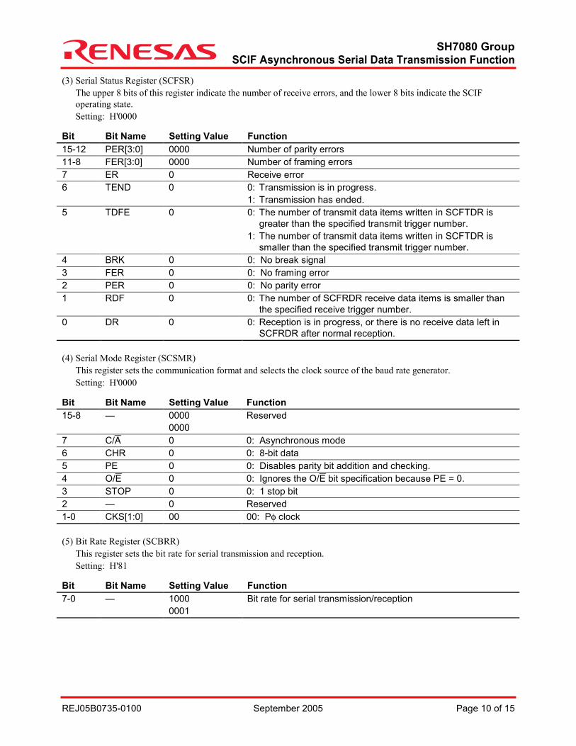
(3) Serial Status Register (SCFSR) The upper 8 bits of this register indicate the number of receive errors, and the lower 8 bits indicate the SCIF operating state. Setting: H'0000
Bit Bit Name Setting Value Function 15-12 PER[3:0] 0000 Number of parity errors 11-8 FER[3:0] 0000 Number of framing errors 7 ER 0 Receive error 6 TEND 0 0: Transmission is in progress.
1: Transmission has ended. 5 TDFE 0 0: The number of transmit data items written in SCFTDR is
greater than the specified transmit trigger number. 1: The number of transmit data items written in SCFTDR is
smaller than the specified transmit trigger number. 4 BRK 0 0: No break signal 3 FER 0 0: No framing error 2 PER 0 0: No parity error 1 RDF 0 0: The number of SCFRDR receive data items is smaller than
the specified receive trigger number. 0 DR 0 0: Reception is in progress, or there is no receive data left in
SCFRDR after normal reception. (4) Serial Mode Register (SCSMR)
This register sets the communication format and selects the clock source of the baud rate generator. Setting: H'0000
Bit Bit Name Setting Value Function 15-8 — 0000
0000 Reserved
7 C/A 0 0: Asynchronous mode 6 CHR 0 0: 8-bit data 5 PE 0 0: Disables parity bit addition and checking. 4 O/E 0 0: Ignores the O/E bit specification because PE = 0. 3 STOP 0 0: 1 stop bit 2 — 0 Reserved 1-0 CKS[1:0] 00 00: Pφ clock (5) Bit Rate Register (SCBRR)
This register sets the bit rate for serial transmission and reception. Setting: H'81
Bit Bit Name Setting Value Function 7-0 — 1000
0001 Bit rate for serial transmission/reception
SH7080 Group SCIF Asynchronous Serial Data Transmission Function
REJ05B0735-0100 September 2005 Page 11 of 15
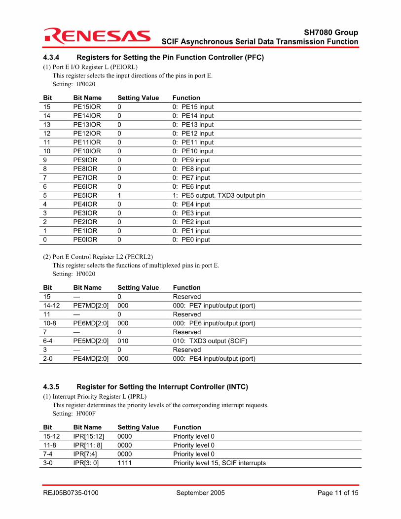
4.3.4 Registers for Setting the Pin Function Controller (PFC) (1) Port E I/O Register L (PEIORL)
This register selects the input directions of the pins in port E. Setting: H'0020
Bit Bit Name Setting Value Function 15 PE15IOR 0 0: PE15 input 14 PE14IOR 0 0: PE14 input 13 PE13IOR 0 0: PE13 input 12 PE12IOR 0 0: PE12 input 11 PE11IOR 0 0: PE11 input 10 PE10IOR 0 0: PE10 input 9 PE9IOR 0 0: PE9 input 8 PE8IOR 0 0: PE8 input 7 PE7IOR 0 0: PE7 input 6 PE6IOR 0 0: PE6 input 5 PE5IOR 1 1: PE5 output. TXD3 output pin 4 PE4IOR 0 0: PE4 input 3 PE3IOR 0 0: PE3 input 2 PE2IOR 0 0: PE2 input 1 PE1IOR 0 0: PE1 input 0 PE0IOR 0 0: PE0 input (2) Port E Control Register L2 (PECRL2)
This register selects the functions of multiplexed pins in port E. Setting: H'0020
Bit Bit Name Setting Value Function 15 — 0 Reserved 14-12 PE7MD[2:0] 000 000: PE7 input/output (port) 11 — 0 Reserved 10-8 PE6MD[2:0] 000 000: PE6 input/output (port) 7 — 0 Reserved 6-4 PE5MD[2:0] 010 010: TXD3 output (SCIF) 3 — 0 Reserved 2-0 PE4MD[2:0] 000 000: PE4 input/output (port)
4.3.5 Register for Setting the Interrupt Controller (INTC) (1) Interrupt Priority Register L (IPRL)
This register determines the priority levels of the corresponding interrupt requests. Setting: H'000F
Bit Bit Name Setting Value Function 15-12 IPR[15:12] 0000 Priority level 0 11-8 IPR[11: 8] 0000 Priority level 0 7-4 IPR[7:4] 0000 Priority level 0 3-0 IPR[3: 0] 1111 Priority level 15, SCIF interrupts
SH7080 Group SCIF Asynchronous Serial Data Transmission Function
REJ05B0735-0100 September 2005 Page 12 of 15
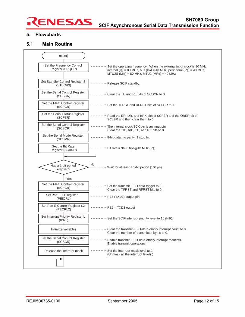
5. Flowcharts
5.1 Main Routine
main()
Set the Frequency Control Register (FRQCR)
Set the operating frequency. When the external input clock is 10 MHz:internal (Iφ) = 80 MHz, bus (Bφ) = 40 MHz, peripheral (Pφ) = 40 MHz, MTU2S (MIφ) = 80 MHz, MTU2 (MPφ) = 40 MHz
Release SCIF standby.Set Standby Control Register 3
(STBCR3)
Clear the TE and RE bits of SCSCR to 0.
Set the TFRST and RFRST bits of SCFCR to 1.
Read the ER, DR, and BRK bits of SCFSR and the ORER bit of SCLSR and then clear them to 0.
The internal clock/SCK pin is an input pin.Clear the TIE, RIE, TE, and RE bits to 0.
8-bit data, no parity, 1 stop bit
Bit rate = 9600 bps@40 MHz (Pφ)
Set the Serial Control Register (SCSCR)
Set the FIFO Control Register (SCFCR)
Set the Serial Status Register (SCFSR)
Set the Serial Control Register (SCSCR)
Set the Serial Mode Register (SCSMR)
Set the Bit Rate Register (SCBRR)
PE5 (TXD3) output pinSet Port E IO Register L
(PEIORL)
Set the transmit FIFO data trigger to 2.Clear the TFRST and RFRST bits to 0.
Set the FIFO Control Register (SCFCR)
Wait for at least a 1-bit period (104 µs)Has a 1-bit period
elapsed?
No
Yes
PE5 = TXD3 output
Set the SCIF interrupt priority level to 15 (H'F).
Clear the transmit-FIFO-data-empty interrupt count to 0.Clear the number of transmitted bytes to 0.
Enable transmit-FIFO-data-empty interrupt requests.Enable transmit operations.
Set the interrupt mask level to 0.(Unmask all the interrupt levels.)
Set Port E Control Register L2 (PECRL2)
Set Interrupt Priority Register L (IPRL)
Initialize variables
Set the Serial Control Register (SCSCR)
Release the interrupt mask
SH7080 Group SCIF Asynchronous Serial Data Transmission Function
REJ05B0735-0100 September 2005 Page 13 of 15
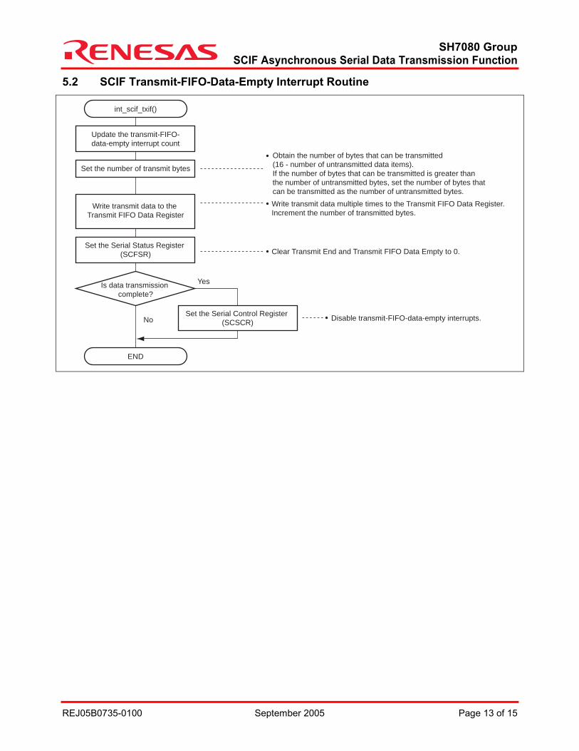
5.2 SCIF Transmit-FIFO-Data-Empty Interrupt Routine
int_scif_txif()
END
Set the number of transmit bytes
Obtain the number of bytes that can be transmitted
(16 - number of untransmitted data items).
If the number of bytes that can be transmitted is greater than
the number of untransmitted bytes, set the number of bytes that
can be transmitted as the number of untransmitted bytes.
Update the transmit-FIFO-
data-empty interrupt count
Write transmit data multiple times to the Transmit FIFO Data Register.
Increment the number of transmitted bytes.Write transmit data to the
Transmit FIFO Data Register
Clear Transmit End and Transmit FIFO Data Empty to 0.Set the Serial Status Register
(SCFSR)
Is data transmission
complete?
Yes
No Disable transmit-FIFO-data-empty interrupts.Set the Serial Control Register
(SCSCR)
SH7080 Group SCIF Asynchronous Serial Data Transmission Function
REJ05B0735-0100 September 2005 Page 14 of 15
Revision Record Description
Rev. Date Page Summary
1.00 Sep.14.05 — First edition issued
SH7080 Group SCIF Asynchronous Serial Data Transmission Function
REJ05B0735-0100 September 2005 Page 15 of 15
1. These materials are intended as a reference to assist our customers in the selection of the Renesas Technology Corp. product best suited to the customer's application; they do not convey any license under any intellectual property rights, or any other rights, belonging to Renesas Technology Corp. or a third party.
2. Renesas Technology Corp. assumes no responsibility for any damage, or infringement of any third-party's rights, originating in the use of any product data, diagrams, charts, programs, algorithms, or circuit application examples contained in these materials.
3. All information contained in these materials, including product data, diagrams, charts, programs and algorithms represents information on products at the time of publication of these materials, and are subject to change by Renesas Technology Corp. without notice due to product improvements or other reasons. It is therefore recommended that customers contact Renesas Technology Corp. or an authorized Renesas Technology Corp. product distributor for the latest product information before purchasing a product listed herein. The information described here may contain technical inaccuracies or typographical errors. Renesas Technology Corp. assumes no responsibility for any damage, liability, or other loss rising from these inaccuracies or errors. Please also pay attention to information published by Renesas Technology Corp. by various means, including the Renesas Technology Corp. Semiconductor home page (http://www.renesas.com).
4. When using any or all of the information contained in these materials, including product data, diagrams, charts, programs, and algorithms, please be sure to evaluate all information as a total system before making a final decision on the applicability of the information and products. Renesas Technology Corp. assumes no responsibility for any damage, liability or other loss resulting from the information contained herein.
5. Renesas Technology Corp. semiconductors are not designed or manufactured for use in a device or system that is used under circumstances in which human life is potentially at stake. Please contact Renesas Technology Corp. or an authorized Renesas Technology Corp. product distributor when considering the use of a product contained herein for any specific purposes, such as apparatus or systems for transportation, vehicular, medical, aerospace, nuclear, or undersea repeater use.
6. The prior written approval of Renesas Technology Corp. is necessary to reprint or reproduce in whole or in part these materials.
7. If these products or technologies are subject to the Japanese export control restrictions, they must be exported under a license from the Japanese government and cannot be imported into a country other than the approved destination. Any diversion or reexport contrary to the export control laws and regulations of Japan and/or the country of destination is prohibited.
8. Please contact Renesas Technology Corp. for further details on these materials or the products contained therein.
1. Renesas Technology Corp. puts the maximum effort into making semiconductor products better and more reliable, but there is always the possibility that trouble may occur with them. Trouble with semiconductors may lead to personal injury, fire or property damage. Remember to give due consideration to safety when making your circuit designs, with appropriate measures such as (i) placement of substitutive, auxiliary circuits, (ii) use of nonflammable material or (iii) prevention against any malfunction or mishap.
Keep safety first in your circuit designs!
Notes regarding these materials