Embed Size (px)
Citation preview

CML Microcircuits
COMMUNICATION SEMICONDUCTORS
DE9941 SDR Demonstrator
User Manual ________________________________________________________________________________________________________
2015 CML Microsystems Plc 2 December 2015 COMPANY CONFIDENTIAL
UM9941/3 December 2015 Provisional Issue
Features
Demonstration of SDR wireless data modem supporting multiple bit rates and modulation schemes.
Provides a demonstration platform for the CMX7164 Multi-mode Modem
Direct Conversion Receiver (CMX994E) and Linear Cartesian Loop Transmitter (CMX998).
On-board PLL and VCO for 452MHz to 467MHz Operation
1W Transmitter Operation Interfaces directly to the PE0003
Designed to meet EN 302 561 Small size – 83mm x 55mm
1 Brief Description
The DE9941 is a small demonstration platform for the CMX994E Direct Conversion Receiver, the CMX998 Cartesian Loop Transmitter and the CMX7164 Multi-mode Wireless Data Modem. The small form factor of the evaluation platform is due to the compact nature of the CML IC solutions. The DE9941 can be used to demonstrate Tx and Rx performance with QAM modulation, FSK and GMSK type modulation. Together with the PE0003 host controller, a full transceiver can be demonstrated using a
Function Image and control scripts. The DE9941 provides a Fractional-N PLL and VCO plus associated circuits to provide local oscillator signals for the CMX994E and CMX998. The PE0003, together with the control scripts, gives the user the ability to program the RF synthesiser to the correct operating frequencies. The design also includes a 1W power amplifier, harmonic filter and Tx/Rx switch. The RF performance is designed to be compliant with EN 302 561 and all the circuits are provided with power-down capability to allow standby functionality. The design is aimed to be low cost, with a minimum number of component types/values.

SDR Demonstrator DE9941
2015 CML Microsystems Plc 2 UM9941/3
CONTENTS Section Page
1 Brief Description .................................................................................................. 1
2 Block Diagram ...................................................................................................... 5
3 Preliminary Information ....................................................................................... 6 3.1 Laboratory Equipment ..................................................................................... 6
3.1.1 Power Supply ............................................................................................ 6 3.2 Handling Precautions ...................................................................................... 6
3.2.1 Static Protection ........................................................................................ 6 3.2.2 Contents - Unpacking ............................................................................... 6
3.3 Approvals ......................................................................................................... 6
4 Quick Start ............................................................................................................ 7 4.1 Setting-Up ........................................................................................................ 7
4.1.1 PE0003 Software and Driver Installation .................................................. 8 4.2 Adjustments ..................................................................................................... 8 4.3 Configuration ................................................................................................... 9
4.3.1 Tx Configuration ........................................................................................ 9 4.3.2 Rx Configuration ....................................................................................... 9
4.4 Operate .......................................................................................................... 10 4.5 Signal Lists .................................................................................................... 11
5 Circuit Schematics and Board Layouts ........................................................... 14
6 Detailed Description .......................................................................................... 17 6.1 Hardware Description .................................................................................... 17
6.1.1 Harmonic Filter ........................................................................................ 17 6.1.2 Tx/Rx Switch ........................................................................................... 17 6.1.3 Coupler .................................................................................................... 17 6.1.4 Power Amplifier ....................................................................................... 17 6.1.5 Transmitter .............................................................................................. 17 6.1.6 Receiver .................................................................................................. 18 6.1.7 Local Oscillator........................................................................................ 18 6.1.8 Reference Oscillator ............................................................................... 18 6.1.9 Power Supply .......................................................................................... 19 6.1.10 Inductors ................................................................................................. 19
6.2 Adjustments and Controls ............................................................................. 19 6.2.1 External/Internal LO ................................................................................ 19
6.3 Software Description ..................................................................................... 19 6.4 Application Information .................................................................................. 19
6.4.1 Scripts ..................................................................................................... 19 6.4.2 Typical Receiver Results with CMX7164 FI-4 ........................................ 23 6.4.3 Typical Transmit Performance with CMX7164 FI-4 ................................ 28
6.5 Troubleshooting ............................................................................................. 35 6.5.1 Receiver Operation ................................................................................. 35 6.5.2 Transmitter Operation ............................................................................. 35
7 Performance Specification ................................................................................ 36 7.1 Electrical Performance .................................................................................. 36
7.1.1 Absolute Maximum Ratings .................................................................... 36 7.1.2 Operating Limits ...................................................................................... 36 7.1.3 Operating Characteristics ....................................................................... 37

SDR Demonstrator DE9941
2015 CML Microsystems Plc 3 UM9941/3
Table Page
Table 1 Signal List ......................................................................................................................... 11 Table 2 PE0003 Interface .............................................................................................................. 11 Table 3 Test Points ........................................................................................................................ 12 Table 4 Adjustments ...................................................................................................................... 13 Table 5 Changes to DE9941 ......................................................................................................... 14 Table 6 Modification State (‘Mod State’) Definitions...................................................................... 14 Table 7 DE9941 Channel Table .................................................................................................... 20 Table 8 Sensitivity levels (mean power) for different gross (on-air) bit rates in a 25kHz channel 24 Table 9 4-QAM Rx Adjacent Channel Rejection with a TETRA interferer at +/-25kHz offset ....... 25 Table 10 16-QAM Rx Adjacent Channel Rejection with a TETRA interferer at +/-25kHz offset ... 26 Table 11 64-QAM Rx Adjacent Channel Rejection with a TETRA interferer at +/-25kHz offset ... 26 Table 12 Co-channel Performance for different gross (on-air) bit rates ........................................ 26 Table 13 Rx Intermodulation Performance for 4-QAM in normal mode ........................................ 27 Table 14 4-QAM Rx Blocking Performance .................................................................................. 28 Table 15 Tx Performance at 459.25MHz with different QAM and Channel Filter Types .............. 28 Table 16 Summary of 16-QAM Tx Output Power and ACP Performance .................................... 29 Table 17 Receiver – Possible Errors ............................................................................................. 35 Table 18 Transmitter – Possible Errors ......................................................................................... 35
Figure Page
Figure 1 Block Diagram ................................................................................................................... 5 Figure 2 Typical Evaluation Connections for DE9941 ..................................................................... 8 Figure 3 PCB Layout: top .............................................................................................................. 15 Figure 4 PCB Layout: bottom ........................................................................................................ 16 Figure 5 Tx Setup 1 ....................................................................................................................... 21 Figure 6 Tx Setup 2 ....................................................................................................................... 22 Figure 7 Rx Sensitivity with 4-QAM, 16-QAM and 64-QAM .......................................................... 24 Figure 8 Rx Sensitivity at different frequencies with 4-QAM ......................................................... 25 Figure 9 4-QAM, 16-QAM and 64-QAM Co-Channel Performance .............................................. 27 Figure 10 16-QAM ACP Performance at 459.75MHz ................................................................... 29 Figure 11 16-QAM ACP Performance at 452.25MHz ................................................................... 30 Figure 12 16-QAM ACP Performance at 467.25MHz ................................................................... 30 Figure 13 16-QAM Constellation at 459.75MHz ............................................................................ 31 Figure 14 16QAM Eye Diagram at 459.75MHz ............................................................................. 31 Figure 15 16-QAM EVM, symbol/error table at 459.75MHz .......................................................... 32 Figure 16 Wideband plots of Tx at 452.25MHz ............................................................................. 32 Figure 17 Wideband plots of Tx at 459.75MHz ............................................................................. 33 Figure 18 Wideband plots of Tx at 467.25MHz ............................................................................. 33 Figure 19 Ramp-up and Ramp-down Profile (QAM) ..................................................................... 33 Figure 20 Tx Ramp Profile (QAM) ................................................................................................. 34
It is always recommended that you check for the latest product datasheet version from the Products page of the CML website: [www.cmlmicro.com].

SDR Demonstrator DE9941
2015 CML Microsystems Plc 4 UM9941/3
History
Version Changes Date
3 Updated to include CMX994E and other relevant changes for mod state 5. 02/12/15
2 Details of modification states 3 and 4 added in section 5. 5/7/13
1 First Issue 19/09/12

SDR Demonstrator DE9941
2015 CML Microsystems Plc 5 UM9941/3
2 Block Diagram
CMX994EI
Q
I
Q
Ref Osc(19.2MHz)
x3
T/R
PA(RF5110G)
RegulatorJ2
PowerPA_Supply
Regulator
Regulator
Regulator
+3V3D_PDSP6
+3V3A_PDSP6
+3V3A_Rx/Tx
+3V3_VCO
J1
Antenna
VCO
2
2
2
2
MAIN
ADC’s
MAIN
DAC’s
AUXADC/
DAC
RAMDAC
GPIO
THRU
CBUS
C-BUS
J3
C-BUS
Interface
Frac-N
PLL
CMX998
5
4
4
4
Rx_EN
TX_RX
J4
External LO
KEY
Interface Connector
Coax Connector
CMX7164
Figure 1 Block Diagram

SDR Demonstrator DE9941
2015 CML Microsystems Plc 6 UM9941/3
3 Preliminary Information The DE9941 provides a RF platform for evaluation of the CMX7164 Multi-mode Wireless Data Modem, with the use of the CMX994E Direct Conversion Receiver and the CMX998 Cartesian Loop Transmitter. A 1W power amplifier has been included plus PLL and VCO for stand-alone operation.
The DE9941 is designed to be used with the PE0003 Evaluation Kit interface Card (see www.cmlmicro.com for more information) which provides controller functionality from a PC interface. PC software is available for use with the PE0003. This software allows scripts to be used to control the CMX7164. All RF circuits are controlled via the CMX7164 C-BUS interface. Various scripts are available for use with the DE9941 and a PE0003 (see section 6.4.1). Alternatively the user may connect their own host controller solution to the control interface (J3).
3.1 Laboratory Equipment The following laboratory equipment is needed to use this evaluation kit:
Power Supply
Spectrum Analyser
RF Signal Generator
Oscilloscope
Personal Computer + PE0003 or other C-BUS microcontroller
For more detailed design or investigation work, additional RF test equipment may be required.
3.1.1 Power Supply The supply input voltage to the PCB is nominally 3.6V (3.5V to 4.0V acceptable). On-board regulators are provided to generate all voltage rails used on the PCB (3.3V). The 3.6V supply should be rated at 2A. NOTE: Care should be exercised with the supplies as they are not protected for reverse polarity. The 3.6V supply directly feeds the power amplifier and it should not exceed 4.8V for nominal operating limits.
3.2 Handling Precautions Like most evaluation kits, this product is designed for use in office and laboratory environments. The following practices will help ensure its proper operation.
3.2.1 Static Protection This product uses low-power CMOS circuits that can be damaged by electrostatic discharge. Partially damaged circuits can function erroneously, leading to misleading results. Observe ESD precautions at all times when handling this product.
3.2.2 Contents - Unpacking Please ensure that you have received all of the items on the separate information sheet (EK9941) and notify CML within seven working days if the delivery is incomplete.
3.3 Approvals This product is not approved to any EMC or other regulatory standard. Users are advised to observe local statutory requirements, which may apply to this product and the radio frequency signals that may emanate from it.

SDR Demonstrator DE9941
2015 CML Microsystems Plc 7 UM9941/3
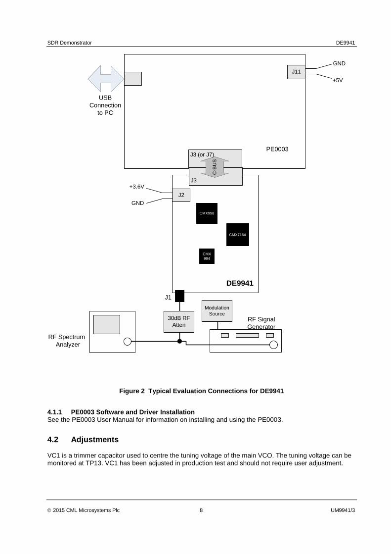
4 Quick Start This section provides instructions for users who wish to experiment immediately with this Evaluation Kit at 459.25MHz. A more complete description of the kit and its uses appears later in this document. The user should read the appropriate CMX7164, CMX994E and CMX998 Datasheets plus the PE0003 User Manuals before using the DE9941 board. This Quick Start configuration assumes that the user has a CML PE0003 Evaluation Kit Interface Card and that the PE0003 provides the interface between DE9941 and a controlling PC.
4.1 Setting-Up The following procedure is recommended:
1. Connect the boards as shown in Figure 2. J1 should be connected to either an RF signal generator or Spectrum analyser via a suitable 50Ω attenuator. If testing the transmitter, the
RF output J1 should be connected to a suitable 50 load.
THE USE OF AN EXTERNAL 50 Ω LOAD IS ESSENTIAL TO PREVENT POSSIBLE DAMAGE TO THE RF POWER AMPLIFIER STAGE.
2. Connect the PE0003 to the DE9941 C-BUS interface connector J3. 3. Apply power to PE0003 and the DE9941. 4. Install the PE0003 software when prompted. – see PE0003 User Manual. 5. The CMX7164 fitted to the DE9941 must be loaded with the required Function Image
TM.This
can be done using the PE0003 GUI. Programming of the RF PLL IC (SKY72300), the CMX994E and the CMX998 is via the PE0003 using a suitable script, for which examples are available (see section 6.4.1).
The board is now ready for operation.
SDR Demonstrator DE9941
2015 CML Microsystems Plc 8 UM9941/3
CMX7164
DE9941
J11
PE0003
USB
Connection
to PC
C-B
US
J3 (or J7)
J3
J2
+5V
GND
-J1
RF Signal
Generator
RF Spectrum
Analyzer
CMX998
+3.6V
GND
CMX
994
30dB RF
Atten
Modulation
Source
Figure 2 Typical Evaluation Connections for DE9941
4.1.1 PE0003 Software and Driver Installation See the PE0003 User Manual for information on installing and using the PE0003.
4.2 Adjustments VC1 is a trimmer capacitor used to centre the tuning voltage of the main VCO. The tuning voltage can be monitored at TP13. VC1 has been adjusted in production test and should not require user adjustment.

SDR Demonstrator DE9941
2015 CML Microsystems Plc 9 UM9941/3
4.3 Configuration The CMX7164 Multi-mode Modem must be loaded with a Function Image (FI) to initialise the device and determine the modulation type; FI-1.x supports GMSK/GFSK, FI-2.x supports 2/4FSK or FI-4.x supports 4/16/64-QAM. This User Manual focuses on FI-4.x because this fully utilities the Tx functionality due to QAM being a non-constant envelope modulation. The following procedures allow the user to quickly setup the DE9941 for Rx or Tx operation.
4.3.1 Tx Configuration The following steps will configure the DE9941 to transmit at 459.25MHz with a continuous 4-QAM PRBS modulated output. Set the applied signals and run the scripts (see section 6.4.1 for details on the scripts) in the order shown in the following table. Note: Ensure J1 is connected to a Spectrum analyser via a suitable 50Ω attenuator for Tx testing. Note: Setting the CML device registers requires the use of the PE0003 host connected as above. The CML datasheets give details of the registers and commands.
Script/Command Setting Note
Setup_Tx_Rx_SDR Script allows selection of;
Mod size
FI
Baud Rate
Tx or Rx
Frequency
Select mod size = 4, FI = 4, mode Tx, Baud rate 18ks/s, Channel No = 8 (Operating Frequency is 459.25MHz).
Tx_only_test_SDR_DCcal
Performs a DC Calibration on the Tx Cartesian loop
After this script has run the Tx output level should be <-25dBm, the output should be nulled unmodulated carrier. Leave PA Enabled.
Write $32 to modem control register ($6B)
Apply Tx PRBS The Tx output will now be at full output power (circa +25dBm mean) continuously. Note: due to limited heatsinking in the compact design it is advised to avoid leaving the Tx in this state for long periods of time.
4.3.2 Rx Configuration The following steps will configure the DE9941 to receive at 459.25MHz with a 2kHz tone IQ output. Set the applied signals and run the scripts (see section 6.4.1 for details on the scripts) as shown in the following table. Note; Ensure J1 is connected to a RF signal generator via a suitable 50Ω attenuator for Rx testing. Note: Setting the CML device registers requires the use of the PE0003 host connected as above. The CML datasheets give details of the registers and commands.
Signal/Script Setting Note
ANTENNA (J1) 459.252MHz The input level here may be user defined: for an input signal of –60dBm at J1, the typical single-ended output level would be ~420mVp-p at U6 pin 28. The output should be a 2kHz sine and cosine wave on I and Q when the configuration in this table is completed.

SDR Demonstrator DE9941
2015 CML Microsystems Plc 10 UM9941/3
Signal/Script Setting Note
Setup_Tx_Rx_SDR Script allows selection of;
Mod Size
FI
Tx or Rx
Baud Rate
Frequency
Select mod size = 4, FI = 4, mode Rx, Baud rate 18ks/s, Channel No = 8 (Operating Frequency is 459.25MHz).
RXIQ (U6)
Rx IQ output. The differential I and Q signals can be measured at U6 pins 28, 29, 31 or 32.
4.4 Operate Following the configuration procedures given in sections 4.1, 4.2 and 4.3, the DE9941 should be operating as a transmitter or receiver at 459.25MHz. Various evaluation tests can now be performed.

SDR Demonstrator DE9941
2015 CML Microsystems Plc 11 UM9941/3
4.5 Signal Lists
CONNECTOR PINOUT
Connector Ref.
Connector
Pin No.
Signal
Name
Signal
Type Description
J1 N/A ANTENNA RF Tx Output or Rx Input
J2 2 +V DC 3.6V Power supply input
J2 1 GNDA DC Power supply ground
Table 1 Signal List
CONNECTOR PINOUT for J3
Connector
Pin No.
Signal
Name
Signal
Type Description
1 RESETN I/P General RESET (RESET active low)
2 CSN I/P C-BUS Enable
3 ~ ~ Spare pin. Leave unconnected
4 CDATA I/P C-BUS Data Input
5 ~ ~ Spare pin. Leave unconnected
6 SCLK I/P C-BUS Clock
7 ~ ~ Spare pin. Leave unconnected
8 RDATA O/P C-BUS Data Output
9 ~ ~ Spare pin. Leave unconnected
10 IRQN I/P Interrupt Request
11 GNDD Power Connection to Digital Ground
12 GNDD Power Connection to Digital Ground
13 ~ ~ Spare pin. Leave unconnected
14 ~ ~ Spare pin. Leave unconnected
15 ~ ~ Spare pin. Leave unconnected
16 ~ ~ Spare pin. Leave unconnected
17 ~ ~ Spare pin. Leave unconnected
18 ~ ~ Spare pin. Leave unconnected
19 ~ ~ Spare pin. Leave unconnected
20 ~ ~ Spare pin. Leave unconnected
Table 2 PE0003 Interface

SDR Demonstrator DE9941
2015 CML Microsystems Plc 12 UM9941/3
TEST POINTS
Test Point Ref.
Default
Measurement Description
TP1 - AUXADC1 – Tx Instability Detector Output
TP2 1.6V DC CMX998 BVRef (Buffered Vref)
TP3 - AUXADC3 – CMX998 Q Feedback Path Output
TP4 - AUXADC4 – CMX998 I Feedback Path Output
TP5 - AUXADC2 – CMX998 DC Meas – used for DC Calibration
TP6 - RF5110G Power Amplifier Control Voltage
TP7 - TXEN+V – Tx/Rx PIN switch supply
TP8 3.3V DC CMX994E Vddio Power Supply Voltage
TP10 - VCO Control Voltage when using CMX994E PLL
TP11 - SKY72300 Frac N Synth Mux Output
TP12 - SKY72300 Frac N Synth Lock Detect Output
TP13 - VCO Control Voltage when using SKY72300 Skyworks Frac N PLL
TP14 - CMX7164 – SYSCLK1
TP15 - CMX7164 – SYSCLK2
TP16 - CMX7164 – Not connected pin
TP17 - CMX7164 – Not connected pin
TP18 - CMX7164 – Not connected pin
TP19 - CMX7164 – Not connected pin
TP20 - CMX7164 – Not connected pin
TP21 - CMX7164 – Not connected pin
TP22 - CMX7164 – Not connected pin
TP23 - CMX7164 – Not connected pin
TP24 - CMX7164 – Not connected pin
TP25 - CMX7164 – MOSI – SPI Data Out
TP26 - CMX7164 – SSOUT1 – SPI Chip Select 1
TP27 - CMX7164 – SSOUT2 – SPI Chip Select 2
TP28 - CMX7164 – CLK – SPI Clock
TP29 - AUXDAC2 – VCTCXO Control Voltage
TP30 3.3V DC CMX7164 Digital Power Supply
TP31 3.3V DC CMX7164 Analogue Power Supply
TP32 3.3V DC Tx and Rx Analogue Power Supply
TP33 3.3V DC VCO and PLL Power Supply
Table 3 Test Points

SDR Demonstrator DE9941
2015 CML Microsystems Plc 13 UM9941/3
ADJUSTMENTS
Adjustment Ref.
Adjustment Adjustment
Range Description
VC1 VCO Tuning 1 - 3V DC Adjustment used to centre the tuning volts of the main
VCO
Table 4 Adjustments
Notes: I/P = Input O/P = Output TP = Test Point

SDR Demonstrator DE9941
2015 CML Microsystems Plc 14 UM9941/3
5 Circuit Schematics and Board Layouts The DE9941 circuit schematic is available as separate high-resolution files, which can be downloaded from the CML website. A 0R link has been added between the analogue and digital ground planes. This has been placed near C87 and C96 on the top layer. The circuit reference on the schematic is R121. Screening is provided over the connector J1, primarily to improve receiver performance.
The layout on each side of the pcb is shown in Figure 3 and Figure 4.
The DE9941 kit was originally released as a Mod State 2 board (dwg9941B02.pdf schematics). Some improvements have been made to the kit and it is currently at Mod State 4 (dwg9941B04.pdf). A list of these modifications appears below, for customers who may wish to update their earlier Mod State boards.
No. Circuit Area & Component Reference
Comment Change
12 C131 VCO
Resonator C
Capacitor tolerance has affected the VCO nominal tuning range, to bring VCO into correct range series C to variable cap has been adjusted.
Change C131 to 3.3pF +/- 0.1pF to
match C128
13 L2 RF5110G Vcc1 Supply
Inductor
Following investigation into transient performance it was found necessary to dampen the PA gain response, most importantly as a function of sharp gain transition over frequency at certain regions of the PA control curve. Adding a 18R at Vcc1 supply choke created this effect (note this is a change indicated in later versions of the RF5110G datasheet application circuit).
Change L2 to 18R 0603 resistor
14 PA Input Pad R58, R60 and
R61
Due to the PA gain reducing because of mod #13 it was necessary to reduce the PA input pad to 6dB.
Change R58 to 39R (0402)
Change R60 and R61 to 150R (0402)
15 C47 PA Control Circuit
See mod #13 relating to transient performance; it was found that in certain regions of the RF5110G control range there were signs of instability, adding a 1µF capacitor at C47 stopped this. Also C47 shapes the PA control curve.
Change C47 to 1µF (0402)
Table 5 Changes to DE9941
Mod State
Changes Hi-Res Schematic
Drawings Date
1 No modifications (B01) 27/4/12
2 Modifications 1-11 (first release) dwg9941B02.pdf 2/8/12
3 As mod state 2 plus modification 12 dwg9941B03.pdf 23/11/12
4 As mod state 3 plus modifications 13 to 15 dwg9941B04.pdf 20/6/13
5 As mod state 4 but with CMX994E fitted instead of CMX994 dwg9941B05.pdf 2/12/15
Table 6 Modification State (‘Mod State’) Definitions
Note: The ‘mod state’ of a particular PCB can be determined from the ‘Board Mod’ box on the PCB.
The number of figures with black dots is the ‘mod state’ thus ‘mod state’ 3 is shown thus:
Board Mod
4
5 6 7 8

SDR Demonstrator DE9941
2015 CML Microsystems Plc 15 UM9941/3
Note Mod state 5 boards include the CMX994E instead of the CMX994 and mod state 4 modifications as listed.
R9
R14R13
C18
R118
R32
R4
0
TP
5T
P4
R106
R6
1R6
0 R58
TP
32
TP
23
TP
22
TP
24
TP
26
TP
6C
89
C7
4
L7
C9
4 C91
L12
L1
3R
96
C164
U9
L4
R8
1
R1
20
TP
33
C143
C6
9
C66
C84
R86
C117
L14
R80
R7
9
C121
L1
6
R8
5R
98
C7
1
C6
5
L6
C1
19
C120
L1
9
TP2C16
R2
2
R21
R16
C23
C32
C26
R33
R31
TP
30
TP16
R37
R107
C8
1
C8
0
TP
21
TP
25
C4
8
C4
6
L9
R5
1
R5
2
C88
C7
6
C7
8
C7
9
TP
27
TP
3
TP
1C
15
6C
87
C5
9
C5
8
L11
C142
C1
62
C1
38
R1
12
R9
9
R111
C62
R7
7
TP
12
TP
10
C1
45
R1
00
C116
L18
TP
13
C111
C112R78
C7
2
C1
24
FL
1
TP
31
T2
R10
R11
R1
2
C20
C1
7
R2
5R
19
TP19
D6
D5
C82
L21
C7
5C68
C67
C57
L2
R5
9
U2
C9
3
C52
C50
C1
TP8
R7
0
TP
29
TP
28
TP
14
C161R109
D3
D2
C7
0
C64
L1
0 L5
C1
10
L17
R82 U4
C144
C12
C3
R2
8
R17
J2
TP17
C21
SW
1
R20
R39
T1
C7
3
C7
7
C55
C54C
56
L3
R8
R6
C90
L8
C1
00
TP11
TP
15
C141
C96
U6
D1
U5
C1
60
TP7
C1
23
C8
3
J1
An
ten
na
R84
12
45
6M
od
3
Se
ria
l N
um
be
r
SC
1
U1
22
0
11
9
J3
U3
TR
4C
10
9
C1
08
TR
5
TP20
R104
R103
TP18
55
.12
5 m
m
82.925 mm
C-B
US
DE
99
41
+V 0V
Figure 3 PCB Layout: top

SDR Demonstrator DE9941
2015 CML Microsystems Plc 16 UM9941/3
C25
C19
R2
6
C4
C5
C3
1
C3
0
R18
R34
C1
78
C1
79
C1
76
C24
R2
7
C35C42
R38
C2
8
C11C10
C165
L2
3
R41
C1
70
C152
R105
C148
R5
0
R69
R67
R65
C9
5
C1
47
C153
R6
2
C158
C159 U8
R5
R97
C181
L15
C1
29
C130
R92
R8
9
L20R
87
C5
3
C1
07
R7
6
C2
2
C1
5
C14
C4
4
R2
4C
15
7
C1
77
C1
75
C29
C1
66
L2
2
U10
R45
R4
4
C1
73
L2
4R
42
R1
01
C47
R66
C9
2C
15
1
C104
C9
9C
98
C8
6
R7
1
R1
10
R57
C180
C1
35
C6
0
C1
27
C5
1
TR6
R5
3R
88
C131
J4
C33 C171R2
3R3
5
C3
4
C13
R3
C2
7
C2R1
R119
R116
D7
R114
R113
R108
C172
C1
74
U12
TR2R49 R36
C105C106
C103C38
C37
C169
R74R75
C97
C1
34 +
C150R6
8
R9
0 R7
2
C1
40
C1
39
C1
67
C1
63
TR3
C4
9
L1
C115
C113
C1
22C125
C136
TR7
R94 R83
C1
28
C1
32
D4 R91
C4
3
R2
R15
R3
0
U7 R115
R2
9
TR1C
10
1
C7
C8
5
C45
C168
R117R48
R4
3
R7
3
C1
54
C155
C133
C36
+C1
49
+C14
6
L25
R63
R1
02
R95
R93
C118
C114
C63C6
1
C126
R5
4
R55
RES1
SC
2
22
0
11
9C1
02
U11
R46
C6
C41
R4
R47
R7
C137
U13
C8C9R5
C39C40-+ VC1
55
.12
5 m
m
82.925 mm
+V0V
Figure 4 PCB Layout: bottom

SDR Demonstrator DE9941
2015 CML Microsystems Plc 17 UM9941/3
6 Detailed Description The DE9941 functionality includes:
Nominal +3.6V Supply
Direct Conversion Receiver
Cartesian Loop Transmitter
1W Power Amplifier
VCO and Fractional-N PLL
19.2MHz VCTCXO
Operation from 452MHz to 467MHz
The C-BUS Interface that allows the card to be connected to a host µController. A PC Interface board is separately available (PE0003) and allows control of all device functions, to support initial test and customer evaluation.
Capability to demonstrate the performance of the CMX7164 Multi-mode Modem, for example 4/16/64-QAM, 2/4FSK and GMSK.
In summary, the DE9941 allows the user to create experiments to investigate all aspects of the CMX7164 device using an RF platform based around the CMX994E Direct Conversion Receiver and the CMX998 Cartesian Loop Transmitter. The DE9941 is designed to allow user modification, to support the detailed investigation of the user’s specific and different applications. The evaluation platform also includes additional circuits that allow the user to use the DE9941 standalone, for example a fractional-N PLL (U5) and a high-frequency VCO (TR6/TR7).
6.1 Hardware Description
6.1.1 Harmonic Filter L5, L6 and associated components form a low-loss low pass filter with taps centred at the 2
nd and 3
rd Tx
harmonics. This filter is common to the transmitter and receiver paths and is connected between the Tx/Rx switch and the antenna connector J1.
6.1.2 Tx/Rx Switch The Tx/Rx switch is a classic series-shunt switch using PIN diodes (D2 and D3) after a lumped quarter wave section. The diodes are activated in transmit via the GPIOC/TXD signal from the CMX7164. An additional diode is provided (at D3), in anti-parallel, to protect the LNA from extremely strong signals (e.g. a nearby transceiver). This branch of the switch then goes to the receiver input.
6.1.3 Coupler The coupler is a lumped coupler formed around one of the low pass sections of the harmonic filter (L5). The signal is coupled from this low pass section to another low pass section (L1) via very low value capacitors (C60 & C61). The coupling factor is ~ 28dB and the output of the coupler forms part of the feedback path to the CMX998 to create the Tx Cartesian Loop.
6.1.4 Power Amplifier The DE9941 includes a 1W Power Amplifier U2 (RF5110G) configured for 450MHz to 470MHz operation and is capable of producing ~+25dBm (mean) output power with 16-QAM modulation. The CMX7164 RAMDAC (AUXDAC1) output is connected to the PA control line via a diode and transistor (D1 and TR2) to provide sufficient current to the PA control pins.
6.1.5 Transmitter The transmitter is based on the CMX998 Cartesian Feedback Loop (CFBL) IC plus the PA and coupler which complete the loop. The up-converter and down-converter are matched with broadband baluns. The LO input is configured for single-ended operation with matching applied for the default DE9941 operating

SDR Demonstrator DE9941
2015 CML Microsystems Plc 18 UM9941/3
frequencies. The LO has been configured single ended as the LO is at four times the final operating frequency (~1.8GHz). The CMX998 IQ differential inputs are provided straight from the CMX7164 main DAC’s. The error amplifier is configured with a loop filter optimised for operation with the on-board power amplifier and for modulation bandwidths up to 25kHz. The DCMEAS pin is connected to an AUXADC on the CMX7164 to allow automatic DC calibration and the ability to control the PA from the CMX7164. The CMX998 is controlled via the CMX7164 SPI-Thru port using chip select 1 (SSOUT1).
6.1.6 Receiver The receiver uses the CMX994E Direct Conversion Receiver IC, capable of supporting a range of digital radio systems of both constant envelope and linear modulation types. The CMX994E integrated LNA has been utilised with the output of the LNA matched directly to the IQ down conversion mixer. The mixer convert the received signal to IQ baseband format, where C87 and C90 combine with on-chip components to remove off-channel signals. The signal is then amplified before further filtering to remove adjacent channel signals (C88 and C89). The nominal maximum bandwidth of the adjacent channel filters is 8kHz and this is scaled by a factor of 2 or 4 in the other filter bandwidth states. A final amplifier stage completes the receiver line-up, providing differential IQ outputs directly to the CMX7164 Main ADC’s. The overall receiver gain and noise figure for the default configuration is ~62.5dB and 7dB respectively. The Rx input third-order intercept point is ~ -2 to -3dBm in normal mode and ~+1 to +2 dBm in enhanced mode. The LO input is at four times the final operating frequency. The CMX994E is controlled via the CMX7164 SPI-Thru port using chip select 1 (SSOUT1).
6.1.7 Local Oscillator The LO (Local Oscillator) for the Tx and the Rx is at four times the final operating frequency. This is achieved with a VCO at 603MHz to 623MHz and then applying a tripler which gives a LO frequency range of 1809MHz to 1869MHz. After the tripler is a SAW filter (FL1 – Golledge MA05897) which reduces all the spurious frequencies from the tripler and ensures that there is enough LO level for the CMX994E and CMX998. There is a buffer stage at the output of the SAW filter. The VCO consists of TR6 and TR7 which are connected in DC cascode and share the same input biasing network. At RF frequencies TR6 works as a common emitter amplifier with the emitter grounded through C126. The oscillator stage is fed to the buffer amplifier through the coupling capacitor C127. To ensure that the frequency range of the VCO can be achieved with good noise performance, a variable capacitor (VC1) has been included to centre the VCO tuning range. The tripler is based around TR5.The final LO buffer is a general purpose silicon bipolar RFIC gain block amplifier (U4 – ADA-4743). At the output of the LO buffer is a 50Ω splitter that feeds the CMX994E and CMX998. The output level from the splitter is ~ -10dBm. The VCO is locked with a Skyworks Fractional N PLL (U5 - SKY72300) controlled via the CMX7164 SPI Thru port and uses chip select 2 (SSOUT2). Circuitry is also included on the board which will allow the user to use the integer-N PLL on the CMX994E if this is desirable over the Frac-N PLL. If required an external LO source can be used instead of the on-board VCO.
6.1.8 Reference Oscillator A 1.5ppm 19.2MHz VCTCXO (Golledge MP05955 is used as the reference for the Frac-N PLL and the CMX7164.

SDR Demonstrator DE9941
2015 CML Microsystems Plc 19 UM9941/3
6.1.9 Power Supply The input to the PCB is nominally 3.6V (3.5V to 4V is acceptable). On-board regulators are provided to generate voltage rails used on the DE9941.
6.1.10 Inductors All inductors used in the RF sections of the design are manufactured by Coilcraft (www.coilcraft.com). Performance of the circuits with inductors from other manufacturers may vary.
6.2 Adjustments and Controls The user has the ability to configure the DE9941 for a number of different operational scenarios.
6.2.1 External/Internal LO The DE9941 has two options for the LO, the default is the on-board VCO plus tripler, SAW filter and buffer. Alternatively, an external LO may be applied at J4 but L15 and R79 should be removed and R82 moved to position R120.
6.3 Software Description Please refer to the PE0003 User Manual for detailed description of the software (see www.cmlmicro.com for more information). The Serial Memory Programming Tab is not applicable with the DE9941. Section 6.4.1 gives detailed information about scripts developed for the DE9941 Evaluation kit. These can be executed through the PE0003 Script Handler.
6.4 Application Information See section 4.1 for board setup details and section 4.3 for operating the DE9941 as a transmitter or receiver.
6.4.1 Scripts The following scripts are available to support the DE9941:
Setup_Tx_Rx_SDR – Must be run first on the Tx and Rx device
Tx_only_test_SDR_DCcal – Only used with the Tx device if a DE9941 is used
SDR_test_ber_tx_rx – BER Script to be run first on the Rx device and then on the Tx device The scripts assume that the user has two PE0003’s, one for Tx and one for Rx. Below is a brief description of what the scripts do:

SDR Demonstrator DE9941
2015 CML Microsystems Plc 20 UM9941/3
Setup_Tx_Rx_SDR This script includes a channel table which allows the PLL to be programmed over the entire operating range of 452.25MHz to 467.25MHz in 1MHz steps. The channel table is shown in Table 7.
Frequency (MHz) Channel No
452.25 1
453.25 2
454.25 3
455.25 4
456.25 5
457.25 6
458.25 7
459.25 8
460.25 9
461.25 10
462.25 11
463.25 12
464.25 13
465.25 14
466.25 15
467.25 16
Table 7 DE9941 Channel Table
The script configures the CMX994E or CMX998 depending on whether it is a transmitter or receiver. The script assumes there are two possible setups for the Tx source: Setup 1 (see Figure 5) and Setup 2 (see Figure 6).

SDR Demonstrator DE9941
2015 CML Microsystems Plc 21 UM9941/3
Setup 1. The Tx is a DE9941.
DE9941
J11
PE0003
USB
Connection
to PC
C-
BU
S
J3 (or J7)
J3
J2
+5V
GND
-J1
+3.6V
GND
>90dB RF
Atten
Rx Input Signal
Figure 5 Tx Setup 1

SDR Demonstrator DE9941
2015 CML Microsystems Plc 22 UM9941/3
Setup 2. The Tx is a PE0601 providing an IQ source to an IQ vector signal generator.
PE0601-xxxx
J11
PE0003
USB
Connection
to PC
C-B
US
J3 (or J7)
J10
J16
+5V
GND
J20
IQ Vector Signal Generator
GND
-5V
J21
J2
3J4
External
Buffer Board
Rx Input Signal
Figure 6 Tx Setup 2
The External Buffer Board shown in Figure 6 provides signal conditioning to ensure that the DC conditions of the IQ input are accurate, so that the carrier suppression of the signal generator output is >40dBc. This setup was used to do the detailed Rx Performance Measurements (see section 6.4.2). This script also sets up the baud rate and channel filters for Tx and Rx. The default channel filter selection in the case of FI-4 is RRC alpha = 0.2. Note: different Tx gain settings (CMX7164 registers B4 and B5) need to be used with the different QAM types and filter types (the script has the nominal gain settings for the alpha = 0.2 case and there are values noted in the script comments for alpha = 0.35).
SDR Demonstrator DE9941
2015 CML Microsystems Plc 23 UM9941/3
Tx_only_test_SDR_DCcal This script only needs to be used with the transmitter when a DE9941 is being used – Setup 1. It performs the CMX998 DC calibration over a requested number of bursts and blocks. For the first blocks sent, a full DC calibration is done and then subsequent calibrations are done in high-gain mode only. The PA is also ramped up and down in this script according to the DC calibration timings. At the end of the DC calibration script, the user has the option to keep the PA enabled. At this point the user can then enable a Tx PRBS transmission by writing $32 to the modem control register ($6B) of the CMX7164 using the PE0003 C-BUS Control Tab. The modulated Tx output will now be at full output power (circa +25dBm mean) continuously. Note: due to limited heat sinking in the compact design it is advised to avoid leaving the Tx in this state for long periods of time.
SDR_test_ber_tx_rx As with the setup script this script assumes that there are two PE0003 boards, one for Tx and one for Rx. The script trains the Receiver Response Equaliser for QAM modulation types and then runs a BER test. The equaliser must be trained with 4-QAM and with an Rx Input signal level of ~ -65 to -60dBm. The default values in the script for the equaliser gain and duration can be used. Further information on the Receiver Response Equaliser can be found in the CMX7164 datasheet. When the equaliser has been trained the user can select the QAM Type but the script assumes that the FI being used is FI-4. The Rx will display the total number of errors at the end of the test with more detailed information being written to a text file. The number of bursts sent is displayed by the transmitter so that the user can confirm the number being received.
6.4.2 Typical Receiver Results with CMX7164 FI-4 The Receiver Response Equaliser within the CMX7164 has been used in single mode to create a channel filter that has compensation for the ADC’s and also the channel filtering within the Rx chain. The AAF (Anti-Alias filter in the CMX7164) is at its default setting of 50kHz, 3 dB bandwidth. The ACR (Adjacent Channel Rejection) filters on the CMX994E are in the maximum bandwidth state (typically 8kHz -3dB bandwidth). In all of the following results the data rate is 18ksymbols/s and, in the following table, the raw over-air bit rate for the three different modulation types have been highlighted. Also, the RRC channel filter used in all cases has an alpha of 0.2. Parametric measurements and graphs shown are typical only, not guaranteed performance limits.
QAM Modulation
Type
Bits per Symbol Base Over-air Bit Rate (18,000 symbols/s)
Raw Mode Over-air Bit Rate (18,000 symbols/s)
4-QAM 2 36,000 bps 32,000 bps
16-QAM 4 72,000 bps 64,000 bps
64-QAM 6 108,000bps 96,000 bps
The difference between the base over-air rate and the raw mode rate (which is the actual user data rate in raw mode at 18ksymbols/second) is due to some symbols being used internally by the modem to perform channel equalisation. All measurements reference ETSI EN 302 561 (v1.2.1 – Dec 2009) specification. All of the detailed receiver performance results were taken with a CML PE0601-7164 and an IQ Vector Signal Generator as the wanted signal. Sensitivity Table 8 shows the EN 302 561 sensitivity specification limits; these limits are to be met at a BER of 10
-2:

SDR Demonstrator DE9941
2015 CML Microsystems Plc 24 UM9941/3
Channel BW Data Rate Sensitivity
38,4 kbit/s or less -111 dBm
25 kHz 38,5 kbits to 76,8 kbit/s -104 dBm
Greater than 76,8 kbit/s -99 dBm
Table 8 Sensitivity levels (mean power) for different gross (on-air) bit rates in a 25kHz channel
Sensitivity results for the DE9941 for 4-QAM, 16-QAM and 64-QAM are shown in Figure 7; the results were taken at 459.25MHz. It can be seen that there is significant margin on the EN 302 561 limits above.
Figure 7 Rx Sensitivity with 4-QAM, 16-QAM and 64-QAM

SDR Demonstrator DE9941
2015 CML Microsystems Plc 25 UM9941/3
The plot in Figure 8 shows the 4-QAM sensitivity performance at the top, middle and bottom of the frequency range; channel 16, 8 and 1 respectively.
Figure 8 Rx Sensitivity at different frequencies with 4-QAM
Adjacent Channel Rejection The adjacent channel rejection was measured with the wanted signal 3 dB above the limit specified in Table 8 and the unwanted signal TETRA modulated at +/-25kHz offset. EN 302 561 states that a BER of less than 10
-2 should be achieved with an interferer level of –63dBm. The results in Table 9 show that this
limit can be met with 4-QAM modulation, with ~8 dB margin.
+25 kHz Offset -25 kHz Offset
Interferer Level (dBm) BER BER
-60 4.75E-05 3.42E-05
-59 1.67E-04
-58 5.85E-04 4.77E-04
-57 1.54E-03
-56 2.92E-03 2.62E-03
-55 6.96E-03
-54 1.39E-02 1.24E-02
Table 9 4-QAM Rx Adjacent Channel Rejection with a TETRA interferer at +/-25kHz offset

SDR Demonstrator DE9941
2015 CML Microsystems Plc 26 UM9941/3
The results in Table 10 show that this limit can be met with 16-QAM modulation, with ~7dB margin.
+25 kHz Offset -25 kHz Offset
Interferer Level (dBm) BER BER
-63 3.33E-06
-62 1.25E-05 7.50E-06
-61 2.42E-05
-60 5.25E-05
-58 6.33E-04 6.03E-04
-56 2.72E-03
-54 1.15E-02 9.93E-03
Table 10 16-QAM Rx Adjacent Channel Rejection with a TETRA interferer at +/-25kHz offset
The results in Table 11 show that this limit can be met with 64-QAM modulation, with ~7dB margin.
+25 kHz Offset -25 kHz Offset
Interferer Level (dBm) BER BER
-62 1.53E-04 1.27E-04
-60 5.81E-04 4.68E-04
-56 6.63E-03 5.54E-03
-55 1.12E-02 9.45E-03
Table 11 64-QAM Rx Adjacent Channel Rejection with a TETRA interferer at +/-25kHz offset
Co-Channel Rejection The co-channel rejection was measured with the wanted signal 3dB above the limit specified in Table 8 and the unwanted signal TETRA modulated on frequency. EN 302 561 co-channel specification limits are as follows and these limits are to be met at a BER of 10
-2:
Channel BW Data Rate Co-channel
38,4 kbit/s or less -12 dB
25 kHz 38,5 kbits to 76,8 kbit/s -19 dB
Greater than 76,8 kbit/s -24 dB
Table 12 Co-channel Performance for different gross (on-air) bit rates
The results for 4-QAM, 16-QAM and 64-QAM co-channel performance are shown in Figure 9. It can be seen that the EN 302 561 can be met in all cases with more than 3 dB margin.

SDR Demonstrator DE9941
2015 CML Microsystems Plc 27 UM9941/3
Figure 9 4-QAM, 16-QAM and 64-QAM Co-Channel Performance
Intermodulation Intermodulation was measured against EN 302 561, which specifies that the wanted tone is 3 dB above the limit specified in Table 8 and the spacing between the unwanted tones is 200kHz for a channel bandwidth of 25 kHz. The first unwanted tone was at 459.45MHz and was un-modulated. The second unwanted tone was at 459.65MHz and was TETRA modulated. The EN 302 561 limit is at an unwanted tone level of –47dBm at a BER of less than 10
-2. The results for 4-QAM are given in Table 13: they show
the EN 302 561 can be met comfortably.
Interferer Level (dBm) BER
Separation (dB)
-42 3.21E-04 66
-41 2.27E-03 67
-40.5 5.67E-03 67.5
-40 1.27E-02 68
Table 13 Rx Intermodulation Performance for 4-QAM in normal mode
Blocking The wanted 4-QAM signal level was –108dBm and an interferer was generated by the HP8642A Low Noise Signal Generator, which was unmodulated. The EN 302 561 interferer level limit is –27dBm with the wanted signal 3 dB up from the sensitivity level in Table 8. The results show that in the 4-QAM mode, the EN 302 561 limit is met comfortably.

SDR Demonstrator DE9941
2015 CML Microsystems Plc 28 UM9941/3
Offset +1MHz -1MHz +2MHz -2MHz +5MHz -5MHz +10MHz -10MHz
Interferer Level (dBm)
Blocker (dBc) BER BER BER BER BER BER BER BER
-20 88 6.50E-05 6.08E-05 1.68E-05
-18 90 8.03E-04 1.56E-03
-17 91 3.86E-03
-16 92 5.05E-03 9.66E-03 2.09E-03 2.00E-03 5.92E-04 7.17E-04 2.12E-04 4.72E-04
Table 14 4-QAM Rx Blocking Performance
Rx Conducted Spurious All spurious are below -80dBm up to 1GHz. High Input Level Performance With AGC ON in the CMX7164, the receiver can be seen to work up to 0dBm with 4-QAM modulation.
6.4.3 Typical Transmit Performance with CMX7164 FI-4 The signal spectrum is identical in bandwidth when using 4-, 16- or 64-QAM. However, the peak-to-mean of each modulation type does vary.
4-QAM has a peak to mean of 5.3dB (=0.2) or 3.8dB (=0.35)
16-QAM has a peak to mean of 7.8dB (=0.2) or 6.4dB (=0.35)
64-QAM has a peak to mean of 9dB (=0.2) or 7.5dB (=0.35)
Table 15 shows some typical measurements at 459.25MHz, with the different QAM and channel filter types. Parametric measurements and graphs shown are typical only, not guaranteed performance limits.
DAC Atten Value B4 & B5 (hex)
Mean O/P Power (dBm)
1st ACP
(dBc)
RRC alpha = 0.2
4-QAM 12 26 65
16-QAM F 24.4 65.5
64-QAM E 23.8 66
RRC alpha = 0.35
4-QAM C 27.5 65/66
16-QAM A 25.7 66
64-QAM 9 25 66/67
Table 15 Tx Performance at 459.25MHz with different QAM and Channel Filter Types
Some further detailed results have been taken with 16-QAM modulation at 18ksymbols/s, with a RRC alpha = 0.2. These results are shown in the following sections.

SDR Demonstrator DE9941
2015 CML Microsystems Plc 29 UM9941/3
16-QAM ACP The plot in Figure 10 was taken at 459.75MHz, Figure 11 is at 452.25MHz and Figure 12 is at 467.25MHz. In all cases the mean output power is >+25 dBm. Note that this includes ~1.2 dB loss through the Tx/Rx switch, harmonic filter/coupler. The peak to mean of 16-QAM is ~7.8 dB, based on a RRC alpha = 0.2 channel filter. A summary of results is shown in Table 16.
452.25MHz 459.75MHz 467.25MHz
Mean output power +25.89dBm +25.57dBm +25.58dBm
1st ACP 65dBc 65dBc 65dBc
2nd
ACP 76dBc 75.5dBc 75dBc
Table 16 Summary of 16-QAM Tx Output Power and ACP Performance
A
31 dB Offset
Unit dBm
RF Att 20 dB
Ref Lvl
30 dBm
Ref Lvl
30 dBm SWT 2.4 s
RBW 500 Hz
VBW 2 kHz
1RM
Center 459.75 MHz Span 118 kHz11.8 kHz/
-60
-50
-40
-30
-20
-10
0
10
20
-70
30
1
Marker 1 [T1]
12.90 dBm
459.75011824 MHz
1 [T1] 12.90 dBm
459.75011824 MHz
CH PWR 25.57 dBm
ACP Up -67.20 dB
ACP Low -66.13 dB
ALT1 Up -75.54 dB
ALT1 Low -76.07 dB
cu2
cu2
cu1
cu1
cl1
cl1
cl2
cl2
C0
C0
Date: 15.MAY.2012 10:20:46
Figure 10 16-QAM ACP Performance at 459.75MHz

SDR Demonstrator DE9941
2015 CML Microsystems Plc 30 UM9941/3
A
31 dB Offset
Unit dBm
RF Att 20 dB
Ref Lvl
30 dBm
Ref Lvl
30 dBm SWT 2.4 s
RBW 500 Hz
11.8 kHz/Center 452.25 MHz Span 118 kHz
VBW 2 kHz
1RM
-60
-50
-40
-30
-20
-10
0
10
20
-70
30
1
Marker 1 [T1]
12.54 dBm
452.25059118 MHz
1 [T1] 12.54 dBm
452.25059118 MHz
CH PWR 25.89 dBm
ACP Up -68.39 dB
ACP Low -67.65 dB
ALT1 Up -77.47 dB
ALT1 Low -76.37 dB
cu2
cu2
cu1
cu1
cl1
cl1
cl2
cl2
C0
C0
Date: 15.MAY.2012 10:19:47
Figure 11 16-QAM ACP Performance at 452.25MHz
A
31 dB Offset
RBW 500 Hz
VBW 2 kHz
SWT 2.4 s Unit dBm
RF Att 20 dB
1RM
Ref Lvl
30 dBm
Ref Lvl
30 dBm
Center 467.25 MHz Span 118 kHz11.8 kHz/
-60
-50
-40
-30
-20
-10
0
10
20
-70
30
1
Marker 1 [T1]
10.20 dBm
467.25035471 MHz
1 [T1] 10.20 dBm
467.25035471 MHz
CH PWR 25.58 dBm
ACP Up -65.96 dB
ACP Low -67.22 dB
ALT1 Up -76.09 dB
ALT1 Low -75.15 dB
cu2
cu2
cu1
cu1
cl1
cl1
cl2
cl2
C0
C0
Date: 15.MAY.2012 11:39:44
Figure 12 16-QAM ACP Performance at 467.25MHz

SDR Demonstrator DE9941
2015 CML Microsystems Plc 31 UM9941/3
16-QAM Constellation, Eye Diagram and EVM In Figure 13 to Figure 15 there are plots of the DE9941 Tx output at 459.75MHz, showing the resultant constellation, eye diagram and EVM.
Ref Lvl
33 dBm 33 dBm
Ref Lvl
33 dBm 33 dBm
31 dB Offset
CF 459.75 MHz
SR 18 kHz
Meas Signal
Vector
Demod 16QAM
IMAG
T1
A
-1.875 1.875 REAL
-1.5
1.5
BURST NOT FOUND
Date: 15.MAY.2012 11:30:50
Figure 13 16-QAM Constellation at 459.75MHz
Ref Lvl
33 dBm 33 dBm
Ref Lvl
33 dBm 33 dBm
A
31 dB Offset
CF 459.75 MHz
SR 18 kHz
Meas Signal
Eye [Q]
Demod 16QAM
IMAG
T1
0 4SYMBOLS
-1
1
BURST NOT FOUND
Date: 15.MAY.2012 11:24:26
Figure 14 16QAM Eye Diagram at 459.75MHz

SDR Demonstrator DE9941
2015 CML Microsystems Plc 32 UM9941/3
Ref Lvl
33 dBm 33 dBm
Ref Lvl
33 dBm 33 dBm
31 dB Offset
CF 459.75 MHz
SR 18 kHz
Symbol/Errors
Demod 16QAM
A
Symbol Table
0 01010110 10100111 00110110 00011001 01000000
40 01100011 00111101 10000001 00000001 00101010
80 01110000 10101100 11010001 01111110 00001111
120 00001100 01111011 01001011 10110110 00110010
160 00011010 10110001 11111100 10101100 00001110
200 01011000 00000111 10011100 00101100 11111010
240 00100100 11010000 00000000 00000110 11100100
280 11000100 01000101 00101010 01001100 01111000
320 10000110 11110000 11110011 01001010 11001110
360 11011010 10100101 10111111 01100000 11010000
400 00111111 11111010 00110000 10010011 11001000
440 01101100 11111001 11101001 10010101 01110011
480 11001110 00110000 10101111 00011100 00111011
520 01110100 10101111 00100000 11100000 00111111
560 00100011 00100010 01100110 01011010 10110010
BURST NOT FOUND Error Summary
Error Vector Mag 1.09 % rms 3.01 % Pk at sym 208
Magnitude Error 0.72 % rms 1.94 % Pk at sym 95
Phase Error 0.66 deg rms 2.10 deg Pk at sym 208
Freq Error 6.33 Hz 6.33 Hz Pk
Amplitude Droop 9.82 dB/sym Rho Factor 0.9998
IQ Offset 0.04 % IQ Imbalance 0.79 %
Date: 15.MAY.2012 11:34:14
Figure 15 16-QAM EVM, symbol/error table at 459.75MHz
Transmit Harmonics and Spurious The following pairs of plots show the DE9941 Tx output at the low (452.25MHz), mid (459.75MHz) and upper (467.25MHz) points of the operating frequency. At each frequency, the plots are taken with a 1MHz span and with a 1GHz span. In all cases the main spurious are those at ~300MHz and 150MHz.
A
31 dB Offset
Unit dBm
RF Att 20 dB
Ref Lvl
30 dBm
Ref Lvl
30 dBm
Center 452.25 MHz Span 1 MHz100 kHz/
RBW 10 kHz
SWT 25 ms
1AVG
VBW 10 kHz
1SA
-60
-50
-40
-30
-20
-10
0
10
20
-70
30
Date: 15.MAY.2012 10:17:11
A
31 dB Offset
Unit dBm
RF Att 20 dB
Ref Lvl
30 dBm
Ref Lvl
30 dBm
Center 500 MHz Span 1 GHz100 MHz/
RBW 3 MHz
VBW 3 MHz
SWT 5 ms
1VIEW 1SA
-60
-50
-40
-30
-20
-10
0
10
20
-70
30
1
Marker 1 [T1]
-37.80 dBm
300.60120240 MHz
1 [T1] -37.80 dBm
300.60120240 MHz
D1 -36 dBm
Date: 15.MAY.2012 10:18:21
Figure 16 Wideband plots of Tx at 452.25MHz

SDR Demonstrator DE9941
2015 CML Microsystems Plc 33 UM9941/3
A
31 dB Offset
Unit dBm
RF Att 20 dB
Ref Lvl
30 dBm
Ref Lvl
30 dBm
1SA
Center 459.75 MHz Span 1 MHz100 kHz/
RBW 10 kHz
VBW 2 kHz
SWT 125 ms
1AVG
-60
-50
-40
-30
-20
-10
0
10
20
-70
30
Date: 15.MAY.2012 10:21:40
A
31 dB Offset
Unit dBm
RF Att 20 dB
Ref Lvl
30 dBm
Ref Lvl
30 dBm
Center 500 MHz Span 1 GHz100 MHz/
RBW 3 MHz
VBW 3 MHz
SWT 5 ms
1VIEW 1SA
-60
-50
-40
-30
-20
-10
0
10
20
-70
30
1
Marker 1 [T1]
-38.38 dBm
306.61322645 MHz
1 [T1] -38.38 dBm
306.61322645 MHz
D1 -36 dBm
Date: 15.MAY.2012 10:22:12
Figure 17 Wideband plots of Tx at 459.75MHz
A
31 dB Offset
Unit dBm
RF Att 20 dB
Ref Lvl
30 dBm
Ref Lvl
30 dBm
Center 467.25 MHz Span 1 MHz100 kHz/
1SA
RBW 10 kHz
VBW 10 kHz
SWT 25 ms
1AVG
-60
-50
-40
-30
-20
-10
0
10
20
-70
30
1
Marker 1 [T1]
21.74 dBm
467.25300601 MHz
1 [T1] 21.74 dBm
467.25300601 MHz
Date: 15.MAY.2012 11:43:52
A
31 dB Offset
Unit dBm
RF Att 20 dB
Ref Lvl
30 dBm
Ref Lvl
30 dBm
Center 500 MHz Span 1 GHz100 MHz/
RBW 3 MHz
VBW 3 MHz
SWT 5 ms
1VIEW 1SA
-60
-50
-40
-30
-20
-10
0
10
20
-70
30
1
Marker 1 [T1]
-35.31 dBm
310.62124248 MHz
1 [T1] -35.31 dBm
310.62124248 MHz
D1 -36 dBm
Date: 15.MAY.2012 11:44:46
Figure 18 Wideband plots of Tx at 467.25MHz
Power and Modulation Ramping Plots in Figure 19 and Figure 20 show the ramp-up and ramp-down profiles using QAM.
Ref Lvl
35 dBm
Ref Lvl
35 dBm
RBW 30 kHz
VBW 30 kHz
RF Att 30 dB
31 dB Offset
A
TRG
Unit dBmSWT 2 ms
Center 459.75 MHz 200 s/
1MA
-60
-50
-40
-30
-20
-10
0
10
20
30
-65
35
1
Marker 1 [T1]
28.20 dBm
893.787575 s
1 [T1] 28.20 dBm
893.787575 s
Date: 17.MAY.2012 17:10:01
Ref Lvl
35 dBm
Ref Lvl
35 dBm
RBW 30 kHz
VBW 30 kHz
RF Att 30 dB
31 dB Offset
A
TRG
Unit dBmSWT 2 ms
Center 459.75 MHz 200 s/
1MA
-60
-50
-40
-30
-20
-10
0
10
20
30
-65
35
1
Marker 1 [T1]
28.10 dBm
893.787575 s
1 [T1] 28.10 dBm
893.787575 s
Date: 17.MAY.2012 17:10:47
Figure 19 Ramp-up and Ramp-down Profile (QAM)

SDR Demonstrator DE9941
2015 CML Microsystems Plc 34 UM9941/3
Ref Lvl
35 dBm
Ref Lvl
35 dBm
RF Att 30 dB
31 dB Offset
A
TRG
Unit dBm
1MA
RBW 30 kHz
VBW 30 kHz
SWT 25 ms
Center 459.75 MHz 2.5 ms/
-60
-50
-40
-30
-20
-10
0
10
20
30
-65
35
1
Marker 1 [T1]
28.19 dBm
893.787575 s
1 [T1] 28.19 dBm
893.787575 s
Date: 17.MAY.2012 17:12:17
Figure 20 Tx Ramp Profile (QAM)

SDR Demonstrator DE9941
2015 CML Microsystems Plc 35 UM9941/3
6.5 Troubleshooting The DE9941 is a complex RF and Baseband system. If incorrectly programmed or modified, results will be at variance from datasheet performance. Please study the CMX7164, CMX998 and CMX994E datasheets, along with the manuals and the associated schematics and layout drawings for these and the DE9941 PCB carefully when troubleshooting. This section provides suggestions to help users resolve application issues they might encounter.
6.5.1 Receiver Operation
Error Observed Possible Cause Remedy
Received data is not provided by the receiver
Incorrect set-up Ensure that suitable values are written to the CMX7164 registers concerning receiver gains and polarity. Also check the dc offsets and signal levels into the CMX7164 IQ Inputs (pins 28, 29, 31 and 32).
Incorrect set-up CMX994E has not been programmed correctly. Check signals as above.
FI not loaded Reset by cycling power. Check checksums.
Synthesiser not locked Incorrect configuration components
Check the SKY72300 synthesiser programming data is correct.
Poor Receiver Performance Receiver Response Equaliser configuration
Ensure single mode equaliser is being used and that training is done with a signal level of ~-65dBm.
Table 17 Receiver – Possible Errors
6.5.2 Transmitter Operation
Error Observed Possible Cause Remedy
Synthesiser not locked Incorrect configuration components
Check that the SKY72300 synthesiser programming data is correct.
Poor Tx modulation spectrum Modulation levels incorrect
Check CMX7164 main DAC attenuator values (B4 and B5) are correct for the QAM and Channel Filter type (see Table 15 for details).
Poor DC Calibration Check nulled carrier condition, i.e. no modulation case. The nulled carrier should typically be <-25dBm.
Poor Wideband Spectrum Incorrect CMX998 Loop Phase Setting
Check values sent to the CMX998 Phase control register.
Low power PIN diode or PA not enabled
Check that the TXEN+V (TP7) power supply is enabled. Also check that the RAMDAC output is being enabled. Check PA control volts at TP6 are ~2.6/2.7Vdc.
Table 18 Transmitter – Possible Errors

SDR Demonstrator DE9941
2015 CML Microsystems Plc 36 UM9941/3
7 Performance Specification
7.1 Electrical Performance
7.1.1 Absolute Maximum Ratings Exceeding these maximum ratings can result in damage to the Evaluation Kit.
Min. Max. Units
Supply (VIN - VSS) 0 4.5 V
Current into or out of VIN and VSS pins 0 +1.5 A
Current into or out of any other connector pin -20 +20 mA Receiver Maximum Input Level +10 dBm
7.1.2 Operating Limits Correct operation of the Evaluation Kit outside these limits is not implied.
Notes Min. Max. Units
Supply (VIN - VSS) 3.5 4.0 V

SDR Demonstrator DE9941
2015 CML Microsystems Plc 37 UM9941/3
7.1.3 Operating Characteristics For the following conditions unless otherwise specified: Xtal Frequency = 19.2MHz, Bit Rate = 18ksymbols/s, Noise Bandwidth = 16kHz, VIN = 3.6V, TAMB = +25°C.
Notes Min. Typ. Max. Units
DC Parameters IIN (on power-up) 1 – 64 68 mA
IIN (FI Loaded only) 1 – 55 58 mA
IIN (Rx enabled and SFS) – 167 – mA
IIN (Rx enabled and Rx Data) – 153 – mA
IIN (Tx and PA enabled, nulled carrier) – 360 – mA
IIN (Tx and PA enabled, modulated carrier) – 1000 1500 mA
AC Parameters Frequency Range 452.25 – 467.25 MHz Tx Mean Output Power 2,3 – 25 – dBm Tx Output Impedance – 50 – Adjacent Channel Power 16-QAM 1
st ACP 2,3 – 66 – dBc
16-QAM 2nd
ACP 2,3 – 75 – dBc Tx EVM 2 – 1 – % Unwanted emission 4 – -36 – dBm Frequency Error – 1.5 – ppm Rx Rx Input Impedance – 50 – Rx Sensitivity 4,5 4-QAM – -116 – dBm 16-QAM – -110 – dBm 64-QAM – -104 – dBm Adjacent Channel Rejection (4-QAM) 4 – -55 – dBm Co-Channel Rejection (4-QAM) 4 – 8 – dB Intermodulation (4-QAM) 4 – -40.5 – dBm Rx Conducted Spurious 4 – < -80 – dBm Maximum Input Level – 0 – dBm Microcontroller Interface For timings see CMX7164 Datasheet
Notes:
1. PCB current consumption, not current consumption of the CML devices. 2. Modulation 16-QAM and RRC alpha = 0.2. 3. 25kHz Channel Spacing and 16kHz Measurement Bandwidth 4. Tested as specified in EN 302 561. BER (Bit Error Rate) is 1 x 10
-2 in all cases in normal
mode. 5. Tx/Rx Channel Filter RRC alpha = 0.2. Receiver Response Equaliser used in single mode.

SDR Demonstrator DE9941
2015 CML Microsystems Plc 38 UM9941/3
CML does not assume any responsibility for the use of any circuitry described. No IPR or circuit patent licences are implied. CML reserves the right at any time without notice to change the said circuitry and any part of this product specification. Evaluation kits and demonstration boards are supplied for the sole purpose of demonstrating the operation of CML products and are supplied without warranty. They are intended for use in a laboratory environment only and are not for re-sale, end-use or incorporation into other equipments. Operation of these kits and boards outside a laboratory environment is not permitted within the European Community. All software/firmware is supplied "as is" and is without warranty. It forms part of the product supplied and is licensed for use only with this product, for the purpose of demonstrating the operation of CML products. Whilst all reasonable efforts are made to ensure that software/firmware contained in this product is virus free, CML accepts no responsibility whatsoever for any contamination which results from using this product and the onus for checking that the software/firmware is virus free is placed on the purchaser of this evaluation kit or development board.