Embed Size (px)
Citation preview

Section 44. Motor Control PWM (MCPWM)
This section of the manual contains the following major topics:
44.1 Introduction .................................................................................................................. 44-2
44.2 Features....................................................................................................................... 44-2
44.3 Control Registers ......................................................................................................... 44-3
44.4 Architecture Overview................................................................................................ 44-37
44.5 Module Description .................................................................................................... 44-39
44.6 PWM Output State Control ........................................................................................ 44-43
44.7 PWM Operating Modes.............................................................................................. 44-46
44.8 PWM Generation ....................................................................................................... 44-61
44.9 Write Protection ......................................................................................................... 44-79
44.10 PWM Output Modes................................................................................................... 44-80
44.11 PWM Generator Triggers ........................................................................................... 44-84
44.12 PWM Interrupts .......................................................................................................... 44-90
44.13 PWM Faults ............................................................................................................... 44-91
44.14 PWM Current-Limit .................................................................................................... 44-96
44.15 Simultaneous PWM Faults and Current-Limits ........................................................ 44-100
44.16 PWM Fault and Current-Limit Trigger Outputs to ADC ............................................ 44-100
44.17 Special Features ...................................................................................................... 44-102
44.18 Power-Saving Modes............................................................................................... 44-117
44.19 External Control of Individual Time Base(s)............................................................. 44-118
44.20 Application Information ............................................................................................ 44-118
44.21 Related Application Notes........................................................................................ 44-130
44.22 Revision History ....................................................................................................... 44-131
© 2017-2018 Microchip Technology Inc. DS60001393B-page 44-1

PIC32 Family Reference Manual
44.1 INTRODUCTION
This section describes the Motor Control Pulse-Width Modulator (MCPWM) module and itsassociated operational modes. The MCPWM module in the PIC32 device family supports awide variety of PWM modes, and is ideal for power conversion/motor control applications.Some of the common applications include:
• SMPS Applications:
- AC-to-DC converters
- DC-to-DC converters
• AC and DC motors (i.e., BDC, BLDC, PMSM, ACIM, SRM)
• Inverters
• Battery chargers
• Digital lighting
• Uninterrupted Power Supply (UPS)
• Power Factor Correction (PFC)
44.2 FEATURES
The MCPWM module consists of the following major features:
• Two master time bases
• Up to 12 PWM generators, each with an individual time base:
- Eight PWM generators with complimentary outputs
- Four additional PWM generators with single-ended outputs
• Individual period, duty cycle, and phase shift registers with on-the-fly updates for each generator
• Duty cycle, dead time, phase shift and frequency resolution generated from the System Clock (SYSCLK)
• Independent fault and current-limit inputs for all 12 PWM generators
• Redundant Output mode
• Secondary Duty Cycle register supports Asymmetric PWM mode
• Push-Pull Output mode
• Complementary Output mode
• Center-Aligned PWM mode
• Output override control
• Special Event Trigger for synchronizing analog-to-digital conversions
• PWM capture feature
• Prescaler for input clock
• Analog-to-Digital Converter (ADC) triggering with PWM
• Leading-edge Blanking (LEB) functionality
• Dead time compensation
• Output clock chopping
• Output pins associated with the PWM module can be individually enabled
• Manual override SFR bits for PWM output pins
Note: This family reference manual section is meant to serve as a complement to devicedata sheets. Depending on the device variant, this manual section may not apply toall PIC32 devices.
Please consult the note at the beginning of the “Motor Control PWM (MCPWM)”chapter in the current device data sheet to check whether this document supportsthe device you are using.
Device data sheets and family reference manual sections are available fordownload from the Microchip Worldwide Web site at: http://www.microchip.com
DS60001393B-page 44-2 © 2017-2018 Microchip Technology Inc.

Section 44. Motor Control PWM (MCPWM)
44.3 CONTROL REGISTERS
The following registers control the operation of the MCPWM module.
44.3.1 Master Time Base Control Registers
• PTCON: PWM Primary Time Base Control Register
This register controls the operation of the primary time base, including enabling or disablingthe MCPWM module, providing module status, setting the special event trigger, triggerpostscaler, and interrupts. In addition, this register can be used to control the PWM outputoverride logic level and prescale the primary PWM input clock.
• PTPER: Primary Master Time Base Period Register
This register stores the synchronization period for the generators that derive their clocksource from the primary master time base.
• SEVTCMP: PWM Primary Special Event Compare Register
This register stores the compare value that is used to trigger the ADC module based on theprimary master time base.
• PMTMR: Primary Master Time Base Timer Register
This register provides the reload synchronization to the generator timers that derive theirclock from the primary master time base.
• STCON Secondary Master Time Base Control Register
This register prescales the secondary PWM input clock, selects the synchronization sourcefor the secondary master time base, and specifies the synchronization setting for secondarymaster time base control.
• STPER: Secondary Master Time Base Period Register
This register stores the synchronization period for the generators that derive their clocksource from the secondary master time base.
• SSEVTCMP: PWM Secondary Special Event Compare Register
This register provides the compare value that is used to trigger the ADC module based onthe secondary master time base.
• SMTMR: Secondary Master Time Base Timer Register
This register provides the reload synchronization to the generator timers that derive theirclock from the secondary master time base.
• CHOP: PWM Chop Clock Generator Register
This register enables/disabled the chop clock generator and provides the chop clockfrequency.
• PWMKEY: PWM Unlock Register
This register accepts the unlock sequence to allow writes to the IOCONx register.
Note: Not all registers are available on all devices. Refer to the “Motor Control PWM(MCPWM)” chapter in the specific device data sheet for availability.
© 2017-2018 Microchip Technology Inc. DS60001393B-page 44-3

PIC32 Family Reference Manual
44.3.2 PWM Generator Control Registers
Each PWM generator has the following set of registers:
• PWMCONx: PWM Control Register ‘x’ (‘x’ = 1 through 12)
This register controls the basic operation of the PWM module, including external PWMReset operation, dead time compensation mode and polarity, enabling/disabling and provid-ing status for Fault, current-limit, and primary target interrupts, as well as selection of thetype of synchronization, the clock source, and alignment mode.
• IOCONx: PWMx I/O Control Register ‘x’ (‘x’ = 1 through 12)
This register controls I/O functions for the PWM module, including PWMxH/PWMxL pin out-put depending on the selected mode, swapping, and output polarity, as well as enabling/dis-abling PWM pin control features and Fault/current-limit override values.
• PDCx: PWM Generator Duty Cycle Register ‘x’ (‘x’ = 1 through 12)
When the MCPWM module is in Edge-Aligned mode, this register specifies the falling edgeinstance of the on-time and controls the duty cycle directly.
When the MCPWM module is in Symmetric Center-Aligned mode, this register controls theinstance when the leading edge transitions state. The SDCx register is automatically copiedwith the value of the PDCx register when updates occur.
When the MCPWM module is in Asymmetric Center-Aligned mode, this register only storesthe leading edge transition compare instance.
• SDCx: PWM Secondary Duty Cycle Register ‘x’ (‘x’ = 1 through 12)
When the MCPWM module is in Edge-Aligned mode, this register is unused.
When the MCPWM module is in Symmetric Center-Aligned mode, this register, althoughfunctional in this mode, is updated transparently to the software. Loads to the PDCx registerautomatically copy over to the SDCx register.
When the MCPWM module is in Asymmetric Center-Aligned mode, the trailing edgecompare instance is stored in this register.
• PHASEx: PWM Primary Phase Shift Register ‘x’ (‘x’ = 1 through 12)
If master time base is selected, this register provides the phase shift value for the PWMxHand PWMxL output. If independent time base is selected, this register provides theindependent time base period for the PWMxH and PWMxL output.
• DTRx: PWM Dead Time Register ‘x’ (‘x’ = 1 through 12)
When the MCPWM module is in Positive Dead Time mode, this register delays the leadingedge of the PWMxH from the trailing edge of the PWMxL.
When the MCPWM module is in Negative Dead Time mode, this register delays the trailingedge of the PWMxH from the leading edge of the PWMxL.
• ALTDTRx: PWM Alternate Dead Time Register ‘x’ (‘x’ = 1 through 12)
When the MCPWM module is in Positive Dead Time mode, this register delays the leadingedge of the PWMxL from the trailing edge of the PWMxH.
When the MCPWM module is in Negative Dead Time mode, this register delays the trailingedge of PWMxL from the leading edge of PWMxH.
• DTCOMPx: Dead Time Compensation Register ‘x’ (‘x’ = 1 through 12)
This register lengthens or shortens the PWMxH/PWMxL on time depending upon the statusof the DTCMPy pin and the DTCP polarity bit. Refer to the Section 44.8.6 “Dead TimeCompensation” for details on Dead Time Compensation.
• TRIGx: PWM Primary Trigger Compare Value Register ‘x’ (‘x’ = 1 through 12)
This register provides the compare value to compare against the local timer PTMRx timebase to generate primary triggers for ADC conversions or interrupts.
• TRGCONx: PWM Trigger Control Register ‘x’ (‘x’ = 1 through 12)
This register enables the PWMx trigger postscaler start event and specifies the number ofPWM cycles to skip before generating the first trigger.
DS60001393B-page 44-4 © 2017-2018 Microchip Technology Inc.

Section 44. Motor Control PWM (MCPWM)
• STRIGx: Secondary PWM Trigger Compare Register ‘x’ (‘x’ = 1 through 12)
This register provides the compare value to compare against the local timer PTMRx timebase to generate secondary triggers for ADC conversions or interrupts.
• CAPx: PWM Timer Capture Register ‘x’ (‘x’ = 1 through 12)
This register provides the captured local time base timer (PTMRx) time base value when aleading edge is detected on the current-limit input, and when LEB processing on thecurrent-limit input signal is completed.
• LEBCONx: Leading-Edge Blanking Control Register ‘x’ (‘x’ = 1 through 12)
This register selects the rising and/or falling edge of the PWMxH and PWMxL outputs forleading-edge blanking (LEB) and enables or disables LEB for fault and current-limit inputs.
• LEBDLYx: Leading-Edge Blanking Delay Register ‘x’ (‘x’ = 1 through 12)
This register provides leading-edge blanking delay for the fault and current-limit inputs.
• AUXCONx: PWM Auxiliary Control Register ‘x’ (‘x’ = 1 through 12)
This register selects the PWM state blank and chop clock sources and the PWMxH andPWMxL output chopping functionality.
• PTMRx: PWM Timer Register ‘x’ (‘x’ = 1 through 12)
This register contains the current value of the PWM time base timer local to each generator.
© 2017-2018 Microchip Technology Inc. DS60001393B-page 44-5

PIC
32 Fam
ily Referen
ce Ma
nu
al
DS
60
00
13
93
B-p
ag
e 4
4-6
© 2
01
7-2
01
8 M
icroch
ip T
ech
no
log
y Inc.
gisters appear after the summary, followed by a
Bit 20/4 Bit 19/3 Bit 18/2 Bit 17/1 Bit 16/0
— — — — —
:0> SEVTPS<3:0>
— — — — —
— — — — —
— — — — —
— — — — —
:0> SEVTPS<3:0>
— — — — —
— — — — —
— — — — —
— — — — —
CLK<9:0>
— — — — —
PWMLIEN PWMHIEN — — —
PTDIR MTBS — XPRES —
RC<3:0> FLTPOL FLTMOD<1:0>
AT<1:0> CLDAT<1:0> SWAP OSYNC
— — — — —
— — — — —
— — — — —
— — — — —
— — — — —
— — — — —
— — — — —
— — — — —
— — — — —
Table 44-1 provides a brief summary of all related Motor Control PWM (MCPWM) module registers. Corresponding redetailed description of each register.
Table 44-1: MCPWM Special Function Register SummaryRegisterName
BitRange Bit 31/15 Bit 30/14 Bit 29/13 Bit 28/12 Bit 27/11 Bit 26/10 Bit 25/9 Bit 24/8 Bit 23/7 Bit 22/6 Bit 21/5
PTCON 31:16 — — — — — — — — — — —
15:0 PTEN — PTSIDL SESTAT SEIEN PWMRDY — — — PCLKDIV<2
PTPER 31:16 — — — — — — — — — — —
15:0 PTPER<15:0>
SEVTCMP 31:16 — — — — — — — — — — —
15:0 SEVTCMP<15:0>
PMTMR 31:16 — — — — — — — — — — —
15:0 PMTMR<15:0>
STCON 31:16 — — — — — — — — — — —
15:0 — — — SSESTAT SSEIEN — — — — SCLKDIV<2
STPER 31:16 — — — — — — — — — — —
15:0 STPER<15:0>
SSEVTCMP 31:16 — — — — — — — — — — —
15:0 SSEVTCMP<15:0>
SMTMR 31:16 — — — — — — — — — — —
15:0 SMTMR<15:0>
CHOP 31:16 — — — — — — — — — — —
15:0 CHPCLKEN — — — — — CHOP
PWMKEY 31:16 — — — — — — — — — — —
15:0 PWMKEY<15:0>
PWMCONx(‘x’ = 1-12)
31:16 FLTIF CLIF TRGIF PWMLIF PWMHIF — — — FLTIEN CLIEN TRGIEN
15:0 FLTSTAT CLTSTAT — — ECAM<1:0> ITB — DTC<1:0> DTCP
IOCONx(‘x’ = 1-12)
31:16 — — CLSRC<3:0> CLPOL CLMOD — FLTS
15:0 PENH PENL POLH POLL PMOD<1:0> OVRENH OVRENL OVRDAT<1:0> FLTD
PDCx(‘x’ = 1-12)
31:16 — — — — — — — — — — —
15:0 PDC<15:0>
SDCx(‘x’ = 1-12)
31:16 — — — — — — — — — — —
15:0 SDC<15:0>
PHASEx(‘x’ = 1-12)
31:16 — — — — — — — — — — —
15:0 PHASE<15:0>
DTRx(‘x’ = 1-12)
31:16 — — — — — — — — — — —
15:0 DTR<15:0>
ALTDTRx(‘x’ = 1-12)
31:16 — — — — — — — — — — —
15:0 ALTDTR<15:0>
DTCOMPx(‘x’ = 1-12)
31:16 — — — — — — — — — — —
15:0 — — DTCOMP<13:0>
TRIGx(‘x’ = 1-12)
31:16 — — — — — — — — — — —
15:0 TRGCMP<15:0>
TRGCONx(‘x’ = 1-12)
31:16 — — — — — — — — — — —
15:0 TRGDIV<3:0> TRGSEL<1:0> STRGSEL<1:0> DTM STRGIS —
Legend: ‘—’ = unimplemented; read as ‘0’.

© 2
01
7-2
01
8 M
icroch
ip T
ech
no
log
y Inc.
DS
60
00
13
93
B-p
ag
e 4
4-7
Se
ction
44. Mo
tor C
on
trol P
WM
(MC
PW
M)
ST(‘x
— — — — —
CA(‘x
— — — — —
LE(‘x
— — — — —
— — — — —
LE(‘x
— — — — —
AU(‘x
— — — — —
HOPSEL<3:0> CHOPHEN CHOPLEN
PT(‘x
— — — — —
Ta
20/4 Bit 19/3 Bit 18/2 Bit 17/1 Bit 16/0
Le
RIGx’ = 1-12)
31:16 — — — — — — — — — — —
15:0 STRGCMP<15:0>
Px’ = 1-12)
31:16 — — — — — — — — — — —
15:0 CAP<15:0>
BCONx’ = 1-12)
31:16 — — — — — — — — — — —
15:0 PHR PHF PLR PLF FLTLEBEN CLLEBEN — — — — —
BDLYx’ = 1-12)
31:16 — — — — — — — — — — —
15:0 — — — — LEB<11:0>
XCONx’ = 1-12)
31:16 — — — — — — — — — — —
15:0 — — — — — — — — — — C
MRx’ = 1-12)
31:16 — — — — — — — — — — —
15:0 TMR<15:0>
ble 44-1: MCPWM Special Function Register Summary (Continued)RegisterName
BitRange Bit 31/15 Bit 30/14 Bit 29/13 Bit 28/12 Bit 27/11 Bit 26/10 Bit 25/9 Bit 24/8 Bit 23/7 Bit 22/6 Bit 21/5 Bit
gend: ‘—’ = unimplemented; read as ‘0’.

PIC32 Family Reference Manual
Register 44-1: PTCON: PWM Primary Time Base Control Register
Bit Range Bit31/23/15/7
Bit30/22/14/6
Bit29/21/13/5
Bit28/20/12/4
Bit27/19/11/3
Bit26/18/10/2
Bit25/17/9/1
Bit24/16/8/0
31:24U-0 U-0 U-0 U-0 U-0 U-0 U-0 U-0
— — — — — — — —
23:16U-0 U-0 U-0 U-0 U-0 U-0 U-0 U-0
— — — — — — — —
15:8R/W-0 U-0 R/W-0 HS/HC-0 R/W-0 HS/HC-0 U-0 U-0
PTEN — PTSIDL SESTAT(1) SEIEN(3) PWMRDY — —
7:0U-0 R/W-0 R/W-0 R/W-0 R/W-0 R/W-0 R/W-0 R/W-0
— PCLKDIV<2:0>(2) SEVTPS<3:0>(2)
Legend: HS = Hardware set HC = Hardware cleared
R = Readable bit W = Writable bit U = Unimplemented bit, read as ‘0’
-n = Value at POR ‘1’ = Bit is set ‘0’ = Bit is cleared x = Bit is unknown
bit 31-16 Unimplemented: Read as ‘0’
bit 15 PTEN: PWM Module Enable bit 1 = PWM module is enabled0 = PWM module is disabled
bit 14 Unimplemented: Read as ‘0’
bit 13 PTSIDL: PWM Time Base Stop in Idle Mode bit1 = PWM time base halts in CPU Idle mode0 = PWM time base runs in CPU Idle mode
bit 12 SESTAT: Special Event Interrupt Status bit(1)
1 = Special Event Interrupt is pending0 = Special Event Interrupt is not pending
bit 11 SEIEN: Special Event Interrupt Enable bit(3)
1 = Special Event Interrupt is enabled0 = Special Event Interrupt is disabled
bit 10 PWMRDY: PWM Module Status bit1 = PWM module is ready and operation has begun0 = PWM module is not ready
bit 9-7 Unimplemented: Read as ‘0’
bit 6-4 PCLKDIV<2:0>: Primary PWM Input Clock Prescaler bits(2)
111 = Divide by 128, PWM resolution = 128/FSYSCLK110 = Divide by 64, PWM resolution = 64/FSYSCLK
•
•
•
000 = Divide by 1, PWM resolution = 1/FSYSCLK (power-on default)
Note 1: The SESTAT bit is cleared by clearing the SEIEN bit and the corresponding bit in the IFSx register.
2: The SEVTPS<3:0> bits should be changed only when the PTEN bit (PTCON<15>) = 0.
3: To clear the Primary Special Event Interrupt, the user application must do the following:
a) Disable the Primary Special Event Interrupt by clearing the SEIEN bit (i.e., setting the bit to ‘0’).
b) Clear the Primary Special Event Interrupt flag by clearing the corresponding bit in the IFSx register.
c) Re-enabling the Primary Special Event Interrupt by setting the SEIEN bit equal to ‘1’, if desired. Theuser application cannot clear the Primary Special Event Interrupt flag as long as the SEIEN bit is equalto ‘1’.
DS60001393B-page 44-8 © 2017-2018 Microchip Technology Inc.
Section 44. Motor Control PWM (MCPWM)
bit 3-0 SEVTPS<3:0>: PWM Special Event Trigger Output Postscaler Select bits(2)
1111 = 1:16 postscaler generates Special Event trigger at every 16th compare match event•
•
•
0001 = 1:2 postscaler generates Special Event trigger at every second compare match event0000 = 1:1 postscaler generates Special Event trigger at every compare match event
Register 44-1: PTCON: PWM Primary Time Base Control Register (Continued)
Note 1: The SESTAT bit is cleared by clearing the SEIEN bit and the corresponding bit in the IFSx register.
2: The SEVTPS<3:0> bits should be changed only when the PTEN bit (PTCON<15>) = 0.
3: To clear the Primary Special Event Interrupt, the user application must do the following:
a) Disable the Primary Special Event Interrupt by clearing the SEIEN bit (i.e., setting the bit to ‘0’).
b) Clear the Primary Special Event Interrupt flag by clearing the corresponding bit in the IFSx register.
c) Re-enabling the Primary Special Event Interrupt by setting the SEIEN bit equal to ‘1’, if desired. Theuser application cannot clear the Primary Special Event Interrupt flag as long as the SEIEN bit is equalto ‘1’.
© 2017-2018 Microchip Technology Inc. DS60001393B-page 44-9

PIC32 Family Reference Manual
Register 44-2: PTPER: Primary Master Time Base Period Register
Bit Range Bit31/23/15/7
Bit30/22/14/6
Bit29/21/13/5
Bit28/20/12/4
Bit27/19/11/3
Bit26/18/10/2
Bit25/17/9/1
Bit24/16/8/0
31:24U-0 U-0 U-0 U-0 U-0 U-0 U-0 U-0
— — — — — — — —
23:16U-0 U-0 U-0 U-0 U-0 U-0 U-0 U-0
— — — — — — — —
15:8R/W-0 R/W-0 R/W-0 R/W-0 R/W-0 R/W-0 R/W-0 R/W-0
PTPER<15:8>(1,2)
7:0R/W-0 R/W-0 R/W-1 R/W-0 R/W-0 R/W-0(3) R/W-0(3) R/W-0(3)
PTPER<7:0>(1,2)
Legend:
R = Readable bit W = Writable bit U = Unimplemented bit, read as ‘0’
-n = Value at POR ‘1’ = Bit is set ‘0’ = Bit is cleared x = Bit is unknown
bit 31-16 Unimplemented: Read as ‘0’
bit 15-0 PTPER<15:0>: Primary Master Time Base Period Value bits(1,2)
Note 1: 1 LSb = 1/FSYSCLK (minimum).
2: Minimum value is 0x0008.
3: If a period value lesser than 0x0008 is chosen, the internal hardware forcefully sets the period to a minimum value of 0x0008.
4: PTPER = (FSYSCLK / (FPWM *(2^ PTCON<PCLKDIV>))); FPWM = User Desired PWM Frequency.
DS60001393B-page 44-10 © 2017-2018 Microchip Technology Inc.

Section 44. Motor Control PWM (MCPWM)
Register 44-3: SEVTCMP: PWM Primary Special Event Compare Register
Bit Range Bit31/23/15/7
Bit30/22/14/6
Bit29/21/13/5
Bit28/20/12/4
Bit27/19/11/3
Bit26/18/10/2
Bit25/17/9/1
Bit24/16/8/0
31:24U-0 U-0 U-0 U-0 U-0 U-0 U-0 U-0
— — — — — — — —
23:16U-0 U-0 U-0 U-0 U-0 U-0 U-0 U-0
— — — — — — — —
15:8R/W-0 R/W-0 R/W-0 R/W-0 R/W-0 R/W-0 R/W-0 R/W-0
SEVTCMP<15:8>
7:0R/W-0 R/W-0 R/W-0 R/W-0 R/W-0 R/W-0 R/W-0 R/W-0
SEVTCMP<7:0>
Legend:
R = Readable bit W = Writable bit U = Unimplemented bit, read as ‘0’
-n = Value at POR ‘1’ = Bit is set ‘0’ = Bit is cleared x = Bit is unknown
bit 31-16 Unimplemented: Read as ‘0’
bit 15-0 SEVTCMP<15:0>: Special Event Compare Count bits
When the contents of this register match the PMTMR value, a special event is generated.
Note 1: 1 LSb = 1/FSYSCLK (minimum)
2: To generate a primary special event trigger at the PWM Period boundary set SEVTCMP = 0. SEVTCMP>= PTPER would not generate any trigger.
Register 44-4: PMTMR: Primary Master Time Base Timer Register
Bit Range Bit31/23/15/7
Bit30/22/14/6
Bit29/21/13/5
Bit28/20/12/4
Bit27/19/11/3
Bit26/18/10/2
Bit25/17/9/1
Bit24/16/8/0
31:24U-0 U-0 U-0 U-0 U-0 U-0 U-0 U-0
— — — — — — — —
23:16U-0 U-0 U-0 U-0 U-0 U-0 U-0 U-0
— — — — — — — —
15:8R-0 R-0 R-0 R-0 R-0 R-0 R-0 R-0
PMTMR<15:8>
7:0R-0 R-0 R-0 R-0 R-0 R-0 R-0 R-0
PMTMR<7:0>
Legend:
R = Readable bit W = Writable bit U = Unimplemented bit, read as ‘0’
-n = Value at POR ‘1’ = Bit is set ‘0’ = Bit is cleared x = Bit is unknown
bit 31-16 Unimplemented: Read as ‘0’
bit 15-0 PMTMR<15:0>: Primary Master Time Base Timer Value bits
This timer increments with each PWM clock until the PTPER value is reached.
© 2017-2018 Microchip Technology Inc. DS60001393B-page 44-11

PIC32 Family Reference Manual
Register 44-5: STCON Secondary Master Time Base Control Register
Bit Range Bit31/23/15/7
Bit30/22/14/6
Bit29/21/13/5
Bit28/20/12/4
Bit27/19/11/3
Bit26/18/10/2
Bit25/17/9/1
Bit24/16/8/0
31:24U-0 U-0 U-0 U-0 U-0 U-0 U-0 U-0
— — — — — — — —
23:16U-0 U-0 U-0 U-0 U-0 U-0 U-0 U-0
— — — — — — — —
15:8U-0 U-0 U-0 HS/HC-0 R/W-0 U-0 U-0 U-0
— — — SSESTAT(1) SSEIEN — — —
7:0U-0 R/W-0 R/W-0 R/W-0 R/W-0 R/W-0 R/W-0 R/W-0
— SCLKDIV<2:0>(2) SEVTPS<3:0>(2)
Legend:
R = Readable bit W = Writable bit U = Unimplemented bit, read as ‘0’
-n = Value at POR ‘1’ = Bit is set ‘0’ = Bit is cleared x = Bit is unknown
bit 31-13 Unimplemented: Read as ‘0’
bit 12 SSESTAT: Secondary Special Event Interrupt Status bit(1)
1 = Secondary Special Event Interrupt is pending0 = Secondary Special Event Interrupt is not pending
bit 11 SSEIEN: Secondary Special Event Interrupt Enable bit
1 = Secondary Special Event Interrupt is enabled0 = Secondary Special Event Interrupt is disabled
bit 10-7 Unimplemented: Read as ‘0’
bit 6-4 SCLKDIV<2:0>: Secondary PWM Input Clock Prescaler(2)
111 = Divide by 128, PWM resolution = 128/FSYSCLK110 = Divide by 64, PWM resolution = 64/FSYSCLK
•
•
•
000 = Divide by 1, PWM resolution = 1/FSYSCLK (power-on default)
bit 3-0 SEVTPS<3:0>: PWM Secondary Special Event Trigger Output Postscaler Select bits(2)
1111 = 1:16 Postscale
•
•
•
0001 = 1:2 Postscale0000 = 1:1 Postscale
Note 1: The SSESTAT bit is cleared by clearing the SSEIEN bit and the corresponding bit in the IFSx register.
2: The SEVTPS<3:0> bits should be changed only when the PTEN bit (PTCON<15>) = 0.
3: To clear the Secondary Special Event Interrupt the user application must do the following:
a) Disable the Secondary Special Event Interrupt by clearing the SEIEN bit (i.e., setting the bit to ‘0’).
b) Clear the Secondary Special Event Interrupt flag by clearing the corresponding bit in the IFSx register.
c) Re-enabling the Secondary Special Event Interrupt by setting the SSEIEN equal to ‘1’, if desired. Theuser application cannot clear the Secondary Special Event Interrupt flag as long as the SSEIEN bit isequal to ‘1’.
DS60001393B-page 44-12 © 2017-2018 Microchip Technology Inc.

Section 44. Motor Control PWM (MCPWM)
Register 44-6: STPER: Secondary Master Time Base Period Register
Bit Range Bit31/23/15/7
Bit30/22/14/6
Bit29/21/13/5
Bit28/20/12/4
Bit27/19/11/3
Bit26/18/10/2
Bit25/17/9/1
Bit24/16/8/0
31:24U-0 U-0 U-0 U-0 U-0 U-0 U-0 U-0
— — — — — — — —
23:16U-0 U-0 U-0 U-0 U-0 U-0 U-0 U-0
— — — — — — — —
15:8R/W-0 R/W-0 R/W-0 R/W-0 R/W-0 R/W-0(3) R/W-0(3) R/W-0(3)
STPER<15:8>(1,2)
7:0R/W-0 R/W-0 R/W-1 R/W-0 R/W-0 R/W-0 R/W-0 R/W-0
STPER<7:0>(1,2)
Legend:
R = Readable bit W = Writable bit U = Unimplemented bit, read as ‘0’
-n = Value at POR ‘1’ = Bit is set ‘0’ = Bit is cleared x = Bit is unknown
bit 31-16 Unimplemented: Read as ‘0’
bit 15-0 STPER<15:0>: Primary Master Time Base Period Value bits(1,2)
Note 1: 1 LSb = 1/FSYSCLK (minimum)
2: Minimum value is 0x0008.
3: If a period value lesser than 0x0008 is chosen, the internal hardware forcefully sets the period to a minimum value of 0x0008.
4: STPER = (FSYSCLK / (FPWM *(2^ PTCON<SCLKDIV>))); FPWM = User Desired PWM Frequency.
Register 44-7: SSEVTCMP: PWM Secondary Special Event Compare Register
Bit Range Bit31/23/15/7
Bit30/22/14/6
Bit29/21/13/5
Bit28/20/12/4
Bit27/19/11/3
Bit26/18/10/2
Bit25/17/9/1
Bit24/16/8/0
31:24U-0 U-0 U-0 U-0 U-0 U-0 U-0 U-0
— — — — — — — —
23:16U-0 U-0 U-0 U-0 U-0 U-0 U-0 U-0
— — — — — — — —
15:8R/W-0 R/W-0 R/W-0 R/W-0 R/W-0 R/W-0 R/W-0 R/W-0
SSEVTCMP<15:8>
7:0R/W-0 R/W-0 R/W-0 R/W-0 R/W-0 R/W-0 R/W-0 R/W-0
SSEVTCMP<7:0>
Legend:
R = Readable bit W = Writable bit U = Unimplemented bit, read as ‘0’
-n = Value at POR ‘1’ = Bit is set ‘0’ = Bit is cleared x = Bit is unknown
bit 31-16 Unimplemented: Read as ‘0’
bit 15-0 SSEVTCMP<15:0>: Secondary Special Event Compare Value bits
When the contents of this register match the SMTMR value, a secondary special event is generated.
Note 1: To generate a secondary special event trigger at the PWM Period boundary set SSEVTCMP = 0. SEVTCMP>= STPER would not generate any trigger.
© 2017-2018 Microchip Technology Inc. DS60001393B-page 44-13
PIC32 Family Reference Manual
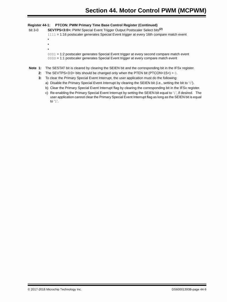
Register 44-8: SMTMR: Secondary Master Time Base Timer Register
Bit Range Bit31/23/15/7
Bit30/22/14/6
Bit29/21/13/5
Bit28/20/12/4
Bit27/19/11/3
Bit26/18/10/2
Bit25/17/9/1
Bit24/16/8/0
31:24U-0 U-0 U-0 U-0 U-0 U-0 U-0 U-0
— — — — — — — —
23:16U-0 U-0 U-0 U-0 U-0 U-0 U-0 U-0
— — — — — — — —
15:8R-0 R-0 R-0 R-0 R-0 R-0 R-0 R-0
SMTMR<15:8>
7:0R-0 R-0 R-0 R-0 R-0 R-0 R-0 R-0
SMTMR<7:0>
Legend:
R = Readable bit W = Writable bit U = Unimplemented bit, read as ‘0’
-n = Value at POR ‘1’ = Bit is set ‘0’ = Bit is cleared x = Bit is unknown
bit 31-16 Unimplemented: Read as ‘0’
bit 15-0 SMTMR<15:0>: Secondary Master Time Base Timer Value bits
This timer increments with each PWM clock until the STPER value is reached.
DS60001393B-page 44-14 © 2017-2018 Microchip Technology Inc.

Section 44. Motor Control PWM (MCPWM)
Register 44-9: CHOP: PWM Chop Clock Generator Register
Bit Range Bit31/2 /15/7
Bit30/22/14/6
Bit29/21/13/5
Bit28/20/12/4
Bit27/19/11/3
Bit26/18/10/2
Bit25/17/9/1
Bit24/16/8/0
31:24U-0 U-0 U-0 U-0 U-0 U-0 U-0 U-0
— — — — — — — —
23:16U-0 U-0 U-0 U-0 U-0 U-0 U-0 U-0
— — — — — — — —
15:8R/W-0 U-0 U-0 U-0 U-0 U-0 R/W-0 R/W-0
CHPCLKEN — — — — — CHOPCLK<9:8>(2,3)
7:0R/W-0 R/W-0 R/W-0 R/W-0 R/W-0 R/W-0 R/W-0 R/W-0
CHOPCLK<7:0>(2,3)
Legend:
R = Readable bit W = Writable bit U = Unimplemented bit, read as ‘0’
-n = Value at POR ‘1’ = Bit is set ‘0’ = Bit is cleared x = Bit is unknown
bit 31-16 Unimplemented: Read as ‘0’
bit 15 CHPCLKEN: Enable Chop Clock Generator bit
1 = Chop clock generator is enabled(1)
0 = Chop clock generator is disabled
bit 14-10 Unimplemented: Read as ‘0’
bit 9-0 CHOPCLK<9:0>: Chop Clock Divider bits(2,3)
Chop Frequency = (FSYSCLK/(2^PTCON<PCLKDIV>)) / (CHOPCLK<9:0>)
Note 1: The chop clock generator operates with the PCLKDIV<2:0> bits (PTCON<6:4>).
2: Minimum values is 0x0002. A value of 0x0000 or 0x0001 will produce no chop clock.
3: These bits should only be changed when the PTEN bit (PTCON<15>) is clear.
Note: The chop clock is a continuous high frequency signal (relative to PWM cycles) that is optionally gated withthe PWM output signals to allow the PWM signals to pass through an external isolation barrier, such as apulse transformer or capacitor. The value of [CHOP<9:0> * PWM clock duration] defines the high and lowtimes of the chop clock. A value of ‘8’ in the CHOP register yields a Chop Clock signal with a period of 16PWM clock cycles as defined by the primary PWM clock prescaler PCLKDIV<2:0.> The value of 0x0000or 0x0001 will produce no chop clock.
© 2017-2018 Microchip Technology Inc. DS60001393B-page 44-15

PIC32 Family Reference Manual
Register 44-10: PWMKEY: PWM Unlock Register
Bit Range Bit31/23/15/7
Bit30/22/14/6
Bit29/21/13/5
Bit28/20/12/4
Bit27/19/11/3
Bit26/18/10/2
Bit25/17/9/1
Bit24/16/8/0
31:24U-0 U-0 U-0 U-0 U-0 U-0 U-0 U-0
— — — — — — — —
23:16U-0 U-0 U-0 U-0 U-0 U-0 U-0 U-0
— — — — — — — —
15:8W-0 W-0 W-0 W-0 W-0 W-0 W-0 W-0
PWMKEY<15:8>
7:0W-0 W-0 W-0 W-0 W-0 W-0 W-0 W-0
PWMKEY<7:0>
Legend:
R = Readable bit W = Writable bit U = Unimplemented bit, read as ‘0’
-n = Value at POR ‘1’ = Bit is set ‘0’ = Bit is cleared x = Bit is unknown
bit 31-16 Unimplemented: Read as ‘0’
bit 15-0 PWMKEY<15:0>: PWM Unlock bits
If the PWMLOCK Configuration bit is asserted (PWMLOCK = 1), the IOCONx registers are writable onlyafter the proper sequence is written to the PWMKEY register. If the PWMLOCK Configuration bit isdeasserted (PWMLOCK = 0), the IOCONx registers are writable at all times. For more information on theunlock sequence, refer to 44.9 “Write Protection”.
This register is implemented only in devices where the PWMLOCK Configuration bit is present in theFOSCSEL Configuration register.
Note: The user must write two consecutive values of 0xABCD and 0x4321 to the PWMKEY register to performan unlock operation if PWMLOCK = 0. Write access to any subsequent secure register must be the verynext access following the unlock process. This is not an atomic operation and any CPU interrupts thatoccur during or immediately after an unlock sequence may cause writes to any PWM secure register to fail.
DS60001393B-page 44-16 © 2017-2018 Microchip Technology Inc.

Section 44. Motor Control PWM (MCPWM)
Register 44-11: PWMCONx: PWM Control Register ‘x’ (‘x’ = 1 through 12)
Bit Range Bit31/23/15/7
Bit30/22/14/6
Bit29/21/13/5
Bit28/20/12/4
Bit27/19/11/3
Bit26/18/10/2
Bit25/17/9/1
Bit24/16/8/0
31:24R/W-0 R/W-0 R/W-0 R/W-0 R/W-0 U-0 U-0 U-0
FLTIF CLIF TRGIF PWMLIF PWMHIF — — —
23:16R/W-0 R/W-0 R/W-0 R/W-0 R/W-0 U-0 U-0 U-0
FLTIEN CLIEN TRGIEN PWMLIEN PWMHIEN — — —
15:8HS/HC-0 HS/HC-0 U-0 U-0 R/W-0 R/W-0 R/W-0 U-0
FLTSTAT(1) CLTSTAT(1) — — ECAM<1:0>(1) ITB(2) —
7:0R/W-0 R/W-0 R/W-0 HS/HC/R-0 R/W-0 U-0 R/W-0 U-0
DTC<1:0> DTCP(4) PTDIR(6) MTBS(7) — XPRES(3) —
Legend:
R = Readable bit W = Writable bit U = Unimplemented bit, read as ‘0’
-n = Value at POR ‘1’ = Bit is set ‘0’ = Bit is cleared x = Bit is unknown
bit 31 FLTIF: Fault Interrupt Flag bit
1 = Fault interrupt has occurred0 = Fault interrupt has not occurred
bit 30 CLIF: Current-Limit Status bit
1 = Current-limit has occurred0 = Current-limit has not occurred
bit 29 TRGIF: Trigger Interrupt Status bit
1 = Trigger interrupt is pending0 = Trigger interrupt is not pending
bit 28 PWMLIF: PWML Interrupt Status bit
1 = PWM period reset interrupt has occurred0 = PWM period reset interrupt has not occurred
bit 27 PWMHIF: PWMH Interrupt Status bit
1 = PWM period match interrupt has occurred0 = PWM period match interrupt has not occurred
bit 26-24 Unimplemented: Read as ‘0’
bit 23 FLTIEN: Fault Interrupt Enable bit
1 = Fault interrupt is enabled. If FLTIF = 1, an interrupt event will be generated.0 = Fault interrupt is disabled
bit 22 CLIEN: Current-Limit Interrupt Enable bit
1 = Current-limit interrupt is enabled. If CLIF = 1, an interrupt event will be generated.0 = Current-limit interrupt is disabled
bit 21 TRIGIEN: Primary Trigger Interrupt Enable bit
1 = A primary trigger event generates an interrupt request0 = A primary trigger event interrupts request is disabled
Note 1: If PWM interrupts are enabled, software must clear the PWMCONx interrupt flags first, followed by the cor-responding IFSx bit in the Interrupt controller. The corresponding PWM IFSx interrupt flag cannot be cleared if any of these local PWMCON interrupt bits are not cleared first. Failure to do so will result in an infinite interrupt loop.
2: This bit should not be changed after the PWM is enabled (PTEN (PTCON<15>) = 1).
3: To operate in External Period Reset mode, the ITB bit must be set to ‘1’ and the CLMOD bit in the IOCONx register must be set to ‘0’.
4: For DTCP to be effective, DTC<1:0> must be set to ‘11’; otherwise, DTCP is ignored.5: Negative dead time is only implemented for Edge-Aligned mode.
6: This bit is only valid and updated during Center-Aligned mode.7: The clock source is one of the master time bases even if ITB = 1 is selected.
© 2017-2018 Microchip Technology Inc. DS60001393B-page 44-17

PIC32 Family Reference Manual
bit 20 PWMLIEN: PWM Low Phase Interrupt Enable bit
1 = When PWM period reset occurs i.e. PWM Timer = 0x0, the PWMLIF flag = 1 and generates an inter-rupt request
0 = PWM Period event interrupt request is disabled
bit 19 PWMHIEN: PWM High Phase Interrupt Enable bit
1 = When the PWM Period matches the value in the PWM timer, an interrupt request is generated0 = PWM Period event interrupt request is disabled, and the PWMHIF bit is cleared
bit 18-16 Unimplemented: Read as ‘0’
bit 15 FLTSTAT: Fault Interrupt Status bit(1)
1 = Fault interrupt is pending0 = No fault interrupt is pendingThis bit is cleared by setting FLTIEN = 0.
bit 14 CLSTAT: Current-Limit Interrupt Status bit(1)
1 = Current-limit interrupt is pending0 = No current-limit interrupt is pendingThis bit is cleared by setting CLIEN = 0.
bit 13-12 Unimplemented: Read as ‘0’
bit 11-10 ECAM<1:0>: Edge/Center-Aligned Mode Enable bits(1)
11 = Asymmetric Center-Aligned mode with simultaneous update10 = Asymmetric Center-Aligned mode01 = Symmetric Center-Aligned mode00 = Edge-Aligned mode
bit 9 ITB: Independent Time Base Mode bit(2)
1 = PHASEx registers provide time base period for this PWM generator0 = PTPER/STPER register provides timing for this PWM generator based on the MTBS bit
bit 8 Unimplemented: Read as ‘0’
bit 7-6 DTC<1:0>: Dead Time Control bits
11 = Dead Time Compensation mode enabled10 = Dead time function is disabled01 = Negative dead time actively applied for Complementary Output mode(5)
00 = Positive dead time actively applied for all output modes
bit 5 DTCP: Dead Time Compensation Polarity bit(5)
1 = If the DTCMPx pin = 0, PWMxL is shortened, and PWMxH is lengthenedIf the DTCMPx pin = 1, PWMxH is shortened, and PWMxL is lengthened
0 = If the DTCMPx pin = 0, PWMxH is shortened, and PWMxL is lengthenedIf the DTCMPx pin = 1, PWMxL is shortened, and PWMxH is lengthened
bit 4 PTDIR: PWM Timer Direction bit(6)
1 = PWM timer is decrementing0 = PWM timer is incrementing
bit 3 MTBS: Master Time Base Select bit(7)
1 = Secondary master time base is the clock source for the MCPWM module0 = Primary master time base is the clock source for the MCPWM module
Register 44-11: PWMCONx: PWM Control Register ‘x’ (‘x’ = 1 through 12) (Continued)
Note 1: If PWM interrupts are enabled, software must clear the PWMCONx interrupt flags first, followed by the cor-responding IFSx bit in the Interrupt controller. The corresponding PWM IFSx interrupt flag cannot be cleared if any of these local PWMCON interrupt bits are not cleared first. Failure to do so will result in an infinite interrupt loop.
2: This bit should not be changed after the PWM is enabled (PTEN (PTCON<15>) = 1).3: To operate in External Period Reset mode, the ITB bit must be set to ‘1’ and the CLMOD bit in the IOCONx
register must be set to ‘0’.4: For DTCP to be effective, DTC<1:0> must be set to ‘11’; otherwise, DTCP is ignored.5: Negative dead time is only implemented for Edge-Aligned mode.6: This bit is only valid and updated during Center-Aligned mode.7: The clock source is one of the master time bases even if ITB = 1 is selected.
DS60001393B-page 44-18 © 2017-2018 Microchip Technology Inc.

Section 44. Motor Control PWM (MCPWM)
bit 2 Unimplemented: Read as ‘0’
bit 1 XPRES: External PWM Reset Control bit(3)
1 = Current-limit source resets primary local time base for this PWM generator if it is in Independent TimeBase mode
0 = External pins do not affect PWM time base
bit 0 Unimplemented: Read as ‘0’
Register 44-11: PWMCONx: PWM Control Register ‘x’ (‘x’ = 1 through 12) (Continued)
Note 1: If PWM interrupts are enabled, software must clear the PWMCONx interrupt flags first, followed by the cor-responding IFSx bit in the Interrupt controller. The corresponding PWM IFSx interrupt flag cannot be cleared if any of these local PWMCON interrupt bits are not cleared first. Failure to do so will result in an infinite interrupt loop.
2: This bit should not be changed after the PWM is enabled (PTEN (PTCON<15>) = 1).3: To operate in External Period Reset mode, the ITB bit must be set to ‘1’ and the CLMOD bit in the IOCONx
register must be set to ‘0’.4: For DTCP to be effective, DTC<1:0> must be set to ‘11’; otherwise, DTCP is ignored.5: Negative dead time is only implemented for Edge-Aligned mode.6: This bit is only valid and updated during Center-Aligned mode.7: The clock source is one of the master time bases even if ITB = 1 is selected.
© 2017-2018 Microchip Technology Inc. DS60001393B-page 44-19

PIC32 Family Reference Manual
Register 44-12: IOCONx: PWMx I/O Control Register ‘x’ (‘x’ = 1 through 12)
Bit Range Bit31/23/15/7
Bit30/22/14/6
Bit29/21/13/5
Bit28/20/12/4
Bit27/19/11/3
Bit26/18/10/2
Bit25/17/9/1
Bit24/16/8/0
31:24U-0 U-0 R/W-0 R/W-0 R/W-0 R/W-0 R/W-0 R/W-0
— — CLSRC<3:0>(2,4) CLPOL(2,4) CLMOD(2,4)
23:16U-0 R/W-1 R/W-1 R/W-1 R/W-1 R/W-0 R/W-0 R/W-0
— FLTSRC<3:0>(2,4) FLTPOL(2) FLTMOD<1:0>(4)
15:8R/W-0 R/W-0 R/W-0 R/W-0 R/W-0 R/W-0 R/W-0 R/W-0
PENH(1) PENL(1) POLH(2) POLL(2) PMOD<1:0>(2) OVRENH OVRENL
7:0R/W-0 R/W-0 R/W-0 R/W-0 R/W-0 R/W-0 R/W-0 R/W-0
OVRDAT<1:0>(3) FLTDAT<1:0>(2,3) CLDAT<1:0> SWAP OSYNC
Legend:
R = Readable bit W = Writable bit U = Unimplemented bit, read as ‘0’
-n = Value at POR ‘1’ = Bit is set ‘0’ = Bit is cleared x = Bit is unknown
bit 31-30 Unimplemented: Read as ‘0’
bit 29-26 CLSRC<3:0>: Current-Limit Control Signal Source select bit for PWM Generator ‘x’(2,4)
These bits specify the current-limit control signal source. Refer to the “Motor Control PWM (MCPWM)” chapter in the specific device data sheet for the available selections.
bit 25 CLPOL: Current-Limit Polarity bits for PWM Generator ‘x’(2,4)
1 = The selected current limit source is active-low0 = The selected current limit source is active-high
bit 24 CLMOD: Current-Limit Mode Enable bit for PWM Generator ‘x’(2,4)
1 = Current-Limit function is enabled0 = Current-Limit function is disabled, current-limit overrides disabled (current-limit interrupts can still be
generated)Changes take effect on the next PWM cycle boundary following PWM being enabled, and subsequentlyon each PWM cycle boundary. When updating CLMOD from ‘1’ to ‘0’, if the current-limit input is still active,the current-limit override condition will not be removed.
bit 23 Unimplemented: Read as ‘0’
bit 22-19 FLTSRC<3:0>: Fault Control Signal Source Select bits for PWM Generator ‘x’(2,4)
These bits specify the Fault control source. Refer to the “Motor Control PWM (MCPWM)” chapter in the specific device data sheet for available selections.
bit 18 FLTPOL: Fault Polarity bits for PWM Generator ‘x’(2)
1 = The selected fault source is active-low0 = The selected fault source is active-high
Note 1: During PWM initialization, if the PWMLOCK fuse bit is 'enabled' (logic '0'), the control on the state of the PWMxL/PWMxH output pins rests solely with the PENH and PENL bits. However, these bits are at '0', which leaves the pin control with the I/O module. Care must be taken to not inadvertently set the TRIS bits to output, which could impose an incorrect output on the PWMxH/PWMxL pins even if there are external pull-up and pull-down resistors. The data direction for the pins must be set to input if tri-state behavior is desired or be driven to the appropriate logic states.The PENH and PENL bits must always be initialized prior to enabling the MCPWM module (PTEN bit = 1).
2: These bits must not be changed after the MCPWM module is enabled (PTEN bit = 1).
3: State represents Active/Inactive state of the PWM, depending on the POLH and POLL bits. For example, if FLTDAT<1> is set to ‘1’ and POLH is set to ‘1’, the PWMxH pin will be at logic level 0 (active level) when a Fault occurs.
4: If (PWMLOCK = 0), these bits are writable only after the proper sequence is written to PWMKEY. If (PWMLOCK = 1), these bits are writable at all times.
DS60001393B-page 44-20 © 2017-2018 Microchip Technology Inc.

Section 44. Motor Control PWM (MCPWM)
bit 17-16 FLTMOD<1:0>: Fault Mode bits for PWM Generator ‘x’(4)
11 = Fault input is disabled, no fault overrides possible. (fault interrupts can still be generated)10 = Reserved01 = Selected fault source forces PWMxH, PWMxL pins to FLTDAT<1:0> values (cycle by cycle)00 = Selected fault source forces PWMxH, PWMxL pins to FLTDAT<1:0> values (Latched condition)Changes take effect on the next PWM cycle boundary following PWM being enabled, and subsequentlyon each PWM cycle boundary. When updating FLTMOD<1:0> from ‘00’ or ‘01’ to ‘11’ (disabled), if thefault input is still active the fault override condition will not be removed.
bit 15 PENH: PWMxH Output Pin Ownership bit(1)
1 = PWM module controls PWMxH pin0 = GPIO module controls PWMxH pin
bit 14 PENL: PWMxL Output Pin Ownership bit(1)
1 = PWM module controls PWMxL pin0 = GPIO module controls PWMxL pin
bit 13 POLH: PWMxH Output Pin Polarity bit(2)
1 = PWMxH pin is active-low0 = PWMxH pin is active-high
bit 12 POLL: PWMxL Output Pin Polarity bit(2)
1 = PWMxL pin is active-low0 = PWMxL pin is active-high
bit 11-10 PMOD<1:0>: PWM ‘x’ I/O Pin Mode bits(2)
11 = PWMxL output is held at logic ‘0’ (adjusted by the POLL bit)10 = PWM I/O pin pair is in Push-Pull Output mode01 = PWM I/O pin pair is in Redundant Output mode00 = PWM I/O pin pair is in Complementary Output mode
bit 9 OVRENH: Override Enable for PWMxH Pin bit
1 = OVRDAT<1> provides data for output on PWMxH pin0 = PWM generator provides data for PWMxH pin
bit 8 OVRENL: Override Enable for PWMxL Pin bit
1 = OVRDAT<0> provides data for output on PWMxL pin0 = PWM generator provides data for PWMxL pin
bit 7-6 OVRDAT<1:0>: State(3) for PWMxH, PWMxL Pins if Override is Enabled bits
If OVRENH = 1, OVRDAT<1> provides data for PWMxHIf OVRENL = 1, OVRDAT<0> provides data for PWMxL
bit 5-4 FLTDAT<1:0>: State(3) for PWMxH and PWMxL Pins if FLTMOD is Enabled bits(2)
If FLTMOD<1:0> (IOCONx<17:16>) = 00 or 01, one of the following Fault modes is enabled:
If fault is active, FLTDAT<1> provides the state for PWMxH
If fault is active, FLTDAT<0> provides the state for PWMxL
If fault is inactive, FLTDAT<1:0> bits are ignored
Register 44-12: IOCONx: PWMx I/O Control Register ‘x’ (‘x’ = 1 through 12) (Continued)
Note 1: During PWM initialization, if the PWMLOCK fuse bit is 'enabled' (logic '0'), the control on the state of the PWMxL/PWMxH output pins rests solely with the PENH and PENL bits. However, these bits are at '0', which leaves the pin control with the I/O module. Care must be taken to not inadvertently set the TRIS bits to output, which could impose an incorrect output on the PWMxH/PWMxL pins even if there are external pull-up and pull-down resistors. The data direction for the pins must be set to input if tri-state behavior is desired or be driven to the appropriate logic states.The PENH and PENL bits must always be initialized prior to enabling the MCPWM module (PTEN bit = 1).
2: These bits must not be changed after the MCPWM module is enabled (PTEN bit = 1).
3: State represents Active/Inactive state of the PWM, depending on the POLH and POLL bits. For example, if FLTDAT<1> is set to ‘1’ and POLH is set to ‘1’, the PWMxH pin will be at logic level 0 (active level) when a Fault occurs.
4: If (PWMLOCK = 0), these bits are writable only after the proper sequence is written to PWMKEY. If (PWMLOCK = 1), these bits are writable at all times.
© 2017-2018 Microchip Technology Inc. DS60001393B-page 44-21

PIC32 Family Reference Manual
bit 3-2 CLDAT<1:0>: State(3) for PWMxH and PWMxL Pins if CLMOD is Enabled bits
If CLMOD (IOCONx<24>) = 1, Current-Limit mode is enabled, as follows:
If current limit is active, CLTDAT<1> provides the state for PWMxH
If current limit is active, CLTDAT<0> provides the state for PWMxL
If current limit is inactive, CLTDAT<1:0> bits are ignored
bit 1 SWAP: SWAP PWMxH and PWMxL Pins bit
1 = PWMxH output signal is connected to PWMxL pin; PWMxL output signal is connected to PWMxH pin0 = PWMxH and PWMxL output signals pins are mapped to their respective pins
bit 0 OSYNC: Output Override Synchronization bit
1 = Output overrides through the OVRDAT<1:0> bits are synchronized to the PWM time base0 = Output overrides through the OVRDAT<1:0> bits occur on next CPU clock boundary
Register 44-12: IOCONx: PWMx I/O Control Register ‘x’ (‘x’ = 1 through 12) (Continued)
Note 1: During PWM initialization, if the PWMLOCK fuse bit is 'enabled' (logic '0'), the control on the state of the PWMxL/PWMxH output pins rests solely with the PENH and PENL bits. However, these bits are at '0', which leaves the pin control with the I/O module. Care must be taken to not inadvertently set the TRIS bits to output, which could impose an incorrect output on the PWMxH/PWMxL pins even if there are external pull-up and pull-down resistors. The data direction for the pins must be set to input if tri-state behavior is desired or be driven to the appropriate logic states.The PENH and PENL bits must always be initialized prior to enabling the MCPWM module (PTEN bit = 1).
2: These bits must not be changed after the MCPWM module is enabled (PTEN bit = 1).
3: State represents Active/Inactive state of the PWM, depending on the POLH and POLL bits. For example, if FLTDAT<1> is set to ‘1’ and POLH is set to ‘1’, the PWMxH pin will be at logic level 0 (active level) when a Fault occurs.
4: If (PWMLOCK = 0), these bits are writable only after the proper sequence is written to PWMKEY. If (PWMLOCK = 1), these bits are writable at all times.
DS60001393B-page 44-22 © 2017-2018 Microchip Technology Inc.

Section 44. Motor Control PWM (MCPWM)
Register 44-13: PDCx: PWM Generator Duty Cycle Register ‘x’ (‘x’ = 1 through 12)
Bit Range Bit31/23/15/7
Bit30/22/14/6
Bit29/21/13/5
Bit28/20/12/4
Bit27/19/11/3
Bit26/18/10/2
Bit25/17/9/1
Bit24/16/8/0
31:24U-0 U-0 U-0 U-0 U-0 U-0 U-0 U-0
— — — — — — — —
23:16U-0 U-0 U-0 U-0 U-0 U-0 U-0 U-0
— — — — — — — —
15:8R/W-0 R/W-0 R/W-0 R/W-0 R/W-0 R/W-0 R/W-0 R/W-0
PDC<15:8>
7:0R/W-0 R/W-0 R/W-0 R/W-0 R/W-0 R/W-0 R/W-0 R/W-0
PDC<7:0>
Legend:
R = Readable bit W = Writable bit U = Unimplemented bit, read as ‘0’
-n = Value at POR ‘1’ = Bit is set ‘0’ = Bit is cleared x = Bit is unknown
bit 31-16 Unimplemented: Read as ‘0’
bit 15-0 PDC<15:0>: PWM Generator Duty Cycle Value bits
If Edge-Aligned mode is enabled (ECAM<1:0> (PWMCONx<11:10>) = 00), these bits specify the trailingedge instance of the ON time and controls the duty cycle directly.
Minimum PWM Resolution = 1 / FSYSCLK.
If one of the Center-Aligned modes is enabled (ECAM<1:0> (PWMCONx<11:10>) = 01, 10, or 11), thesebits specify the compare instance to 'leading edge' level transition.
Minimum PWM Resolution = 2 / FSYSCLK.
Note 1: In Independent PWM mode, PMOD<1:0> (IOCONx<11:10>) = 11, the PDCx register controls the PWMxHduty cycle only. In Complementary, Redundant and Push-Pull PWM modes (PMOD<1:0> = 00, 01, or 10),the PDCx register controls the duty cycle of both the PWMxH and PWMxL.
© 2017-2018 Microchip Technology Inc. DS60001393B-page 44-23

PIC32 Family Reference Manual
Register 44-14: SDCx: PWM Secondary Duty Cycle Register ‘x’ (‘x’ = 1 through 12)
Bit Range Bit31/23/15/7
Bit30/22/14/6
Bit29/21/13/5
Bit28/20/12/4
Bit27/19/11/3
Bit26/18/10/2
Bit25/17/9/1
Bit24/16/8/0
31:24U-0 U-0 U-0 U-0 U-0 U-0 U-0 U-0
— — — — — — — —
23:16U-0 U-0 U-0 U-0 U-0 U-0 U-0 U-0
— — — — — — — —
15:8R/W-0 R/W-0 R/W-0 R/W-0 R/W-0 R/W-0 R/W-0 R/W-0
SDC<15:8>
7:0R/W-0 R/W-0 R/W-0 R/W-0 R/W-0 R/W-0 R/W-0 R/W-0
SDC<7:0>
Legend:
R = Readable bit W = Writable bit U = Unimplemented bit, read as ‘0’
-n = Value at POR ‘1’ = Bit is set ‘0’ = Bit is cleared x = Bit is unknown
bit 31-16 Unimplemented: Read as ‘0’
bit 15-0 SDC<15:0>: Secondary Duty Cycle bits for PWMxL output pin
If Edge-Aligned mode is enabled (ECAM<1:0> (PWMCONx<11:10>) = 00) these bits are unused.
If Symmetric Center-Aligned mode is enabled (ECAM<1:0> (PWMCONx<11:10>) = 01), these bits areupdated transparently to the user. Loads to the PDCx register automatically copy over to the SDCxregister.
If Asymmetric Center-Aligned mode is enabled (ECAM<1:0> (PWMCONx<11:10>) = 10 or 11), these bits specify the compare instance for 'trailing edge' level transition.
DS60001393B-page 44-24 © 2017-2018 Microchip Technology Inc.

Section 44. Motor Control PWM (MCPWM)
Register 44-15: PHASEx: PWM Primary Phase Shift Register ‘x’ (‘x’ = 1 through 12)
Bit Range Bit31/23/15/7
Bit30/22/14/6
Bit29/21/13/5
Bit28/20/12/4
Bit27/19/11/3
Bit26/18/10/2
Bit25/17/9/1
Bit24/16/8/0
31:24U-0 U-0 U-0 U-0 U-0 U-0 U-0 U-0
— — — — — — — —
23:16U-0 U-0 U-0 U-0 U-0 U-0 U-0 U-0
— — — — — — — —
15:8R/W-0 R/W-0 R/W-0 R/W-0 R/W-0 R/W-0 R/W-0 R/W-0
PHASE<15:8>
7:0R/W-0 R/W-0 R/W-0 R/W-0 R/W-0 R/W-0 R/W-0 R/W-0
PHASE<7:0>
Legend:
R = Readable bit W = Writable bit U = Unimplemented bit, read as ‘0’
-n = Value at POR ‘1’ = Bit is set ‘0’ = Bit is cleared x = Bit is unknown
bit 31-16 Unimplemented: Read as ‘0’
bit 15-0 PHASE<15:0>: PWM Phase Shift Value or Independent Time Base Period(5) bits for the PWM Generator
Note 1: If the ITB bit (PWMCONx<9>) = 0, the following applies based on the mode of operation:
Complementary, Redundant and Push-Pull Output modes (PMOD<1:0> (IOCONx<11:10>) = 00, 01, or10) PHASE<15:0> = Phase shift value for PWMxH and PWMxL outputs
2: If the ITB bit = 1, the following applies based on the mode of operation:
Complementary, Redundant, and Push-Pull Output modes (PMOD<1:0> = 00, 01, or 10)PHASE<15:0> = local time base period value for PTMRx
3: A Phase offset that exceeds the PWM period will lead to unpredictable results.
4: The minimum period value when ITB = 1 is 0x0008.
5: Refer to Equation 44-1 and Equation 44-3 for period calculation in edge-aligned and center-aligned modesrespectively.
© 2017-2018 Microchip Technology Inc. DS60001393B-page 44-25

PIC32 Family Reference Manual
Register 44-16: DTRx: PWM Dead Time Register ‘x’ (‘x’ = 1 through 12)
Bit Range Bit31/23/15/7
Bit30/22/14/6
Bit29/21/13/5
Bit28/20/12/4
Bit27/19/11/3
Bit26/18/10/2
Bit25/17/9/1
Bit24/16/8/0
31:24U-0 U-0 U-0 U-0 U-0 U-0 U-0 U-0
— — — — — — — —
23:16U-0 U-0 U-0 U-0 U-0 U-0 U-0 U-0
— — — — — — — —
15:8U-0 U-0 R/W-0 R/W-0 R/W-0 R/W-0 R/W-0 R/W-0
— — DTR<13:8>
7:0R/W-0 R/W-0 R/W-0 R/W-0 R/W-0 R/W-0 R/W-0 R/W-0
DTR<7:0>
Legend:
R = Readable bit W = Writable bit U = Unimplemented bit, read as ‘0’
-n = Value at POR ‘1’ = Bit is set ‘0’ = Bit is cleared x = Bit is unknown
bit 31-16 Unimplemented: Read as ‘0’
bit 15-0 DTR<13:0>: Unsigned 14-bit Dead Time Value for PWMxH Dead Time Unit bits
These bits specify the leading edge dead time count between the PWMxH and PWMxL. The time base for the count is the same as for the PWM generator.
Note: The dead time period is typically set equal to the switching times of the power transistors in the applicationcircuits. It is specifically intended for use in Complementary Output mode. The use of dead time in anyother mode may generate unexpected or unpredictable results. If the duty cycle value in the PDCx/SDCxregister equals ‘0’, or is greater than or equal to the Period, dead time compensation is ignored. The valuesfor Duty Cycle + Dead Time + Dead Time Compensation must not exceed the value for the Period registerminus 1. If the sum exceeds the Period Register - 1, unexpected results may occur. The values for DutyCycle + Dead Time - Dead Time Compensation must be greater than ‘0’, or unexpected results may occur.
DS60001393B-page 44-26 © 2017-2018 Microchip Technology Inc.

Section 44. Motor Control PWM (MCPWM)
Register 44-17: ALTDTRx: PWM Alternate Dead Time Register ‘x’ (‘x’ = 1 through 12)
Bit Range Bit31/23/15/7
Bit30/22/14/6
Bit29/21/13/5
Bit28/20/12/4
Bit27/19/11/3
Bit26/18/10/2
Bit25/17/9/1
Bit24/16/8/0
31:24U-0 U-0 U-0 U-0 U-0 U-0 U-0 U-0
— — — — — — — —
23:16U-0 U-0 U-0 U-0 U-0 U-0 U-0 U-0
— — — — — — — —
15:8U-0 U-0 R/W-0 R/W-0 R/W-0 R/W-0 R/W-0 R/W-0
— — ALTDTR<13:8>
7:0R/W-0 R/W-0 R/W-0 R/W-0 R/W-0 R/W-0 R/W-0 R/W-0
ALTDTR<7:0>
Legend:
R = Readable bit W = Writable bit U = Unimplemented bit, read as ‘0’
-n = Value at POR ‘1’ = Bit is set ‘0’ = Bit is cleared x = Bit is unknown
bit 31-16 Unimplemented: Read as ‘0’
bit 15-0 ALTDTR<13:0>: Unsigned 14-bit Dead Time Value for PWMxL Dead Time Unit bits
These bits specify the trailing edge dead time count between the PWMxH and PWMxL. The time base for the count is the same as for the PWM generator.
Note: The alternate dead time period is typically set equal to the switching times of the power transistors in theapplication circuits. It is specifically intended for use in Complementary Output mode. The use of dead timein any other mode may generate unexpected or unpredictable results. If the duty cycle value in thePDCx/SDCx register equals ‘0’, or is greater than or equal to the Period, alternate dead time compensationis ignored. The values for Duty Cycle + Dead Time + Alternate Dead Time Compensation must not exceedthe value for the Period Register - 1. If the sum exceeds the Period Register -1, unexpected results mayoccur. The values for Duty Cycle + Dead Time - Alternate Dead Time Compensation must be greater than‘0’, or unexpected results may occur.
© 2017-2018 Microchip Technology Inc. DS60001393B-page 44-27
PIC32 Family Reference Manual
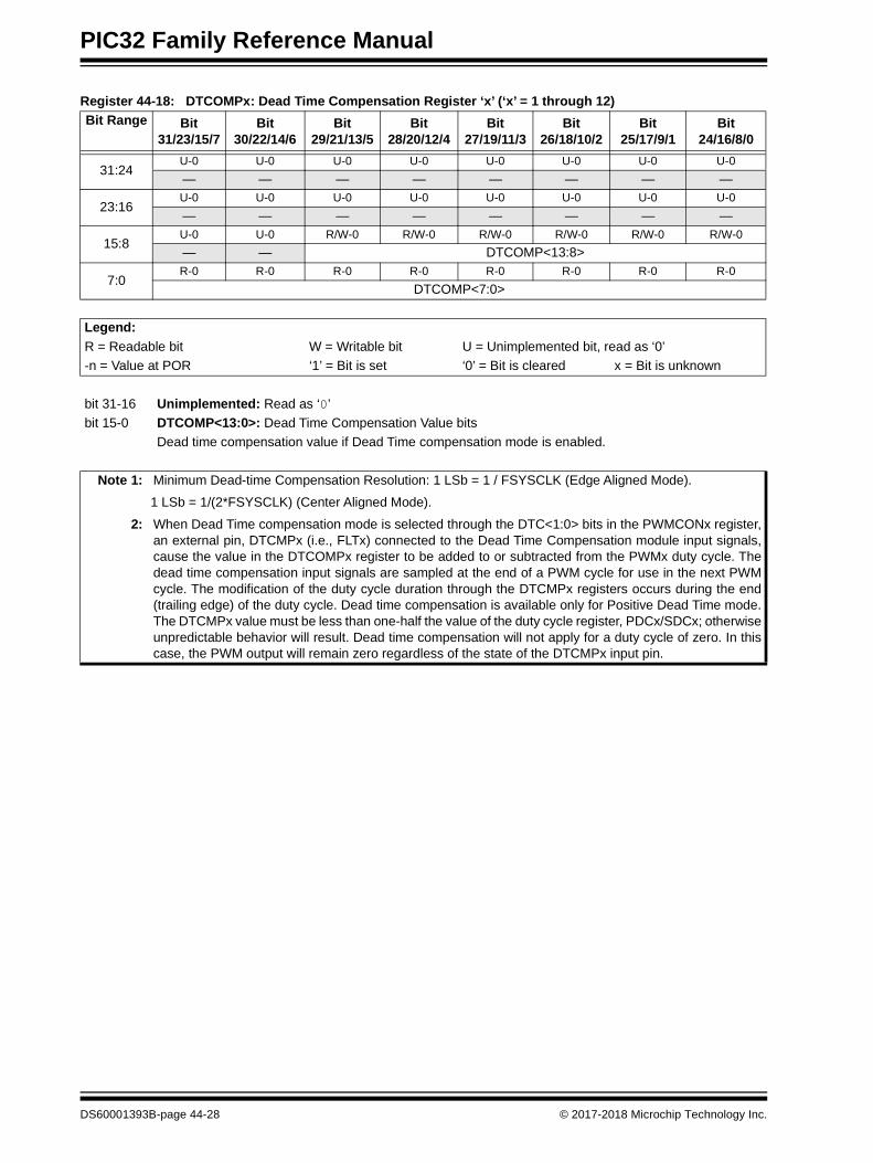
Register 44-18: DTCOMPx: Dead Time Compensation Register ‘x’ (‘x’ = 1 through 12)
Bit Range Bit31/23/15/7
Bit30/22/14/6
Bit29/21/13/5
Bit28/20/12/4
Bit27/19/11/3
Bit26/18/10/2
Bit25/17/9/1
Bit24/16/8/0
31:24U-0 U-0 U-0 U-0 U-0 U-0 U-0 U-0
— — — — — — — —
23:16U-0 U-0 U-0 U-0 U-0 U-0 U-0 U-0
— — — — — — — —
15:8U-0 U-0 R/W-0 R/W-0 R/W-0 R/W-0 R/W-0 R/W-0
— — DTCOMP<13:8>
7:0R-0 R-0 R-0 R-0 R-0 R-0 R-0 R-0
DTCOMP<7:0>
Legend:
R = Readable bit W = Writable bit U = Unimplemented bit, read as ‘0’
-n = Value at POR ‘1’ = Bit is set ‘0’ = Bit is cleared x = Bit is unknown
bit 31-16 Unimplemented: Read as ‘0’
bit 15-0 DTCOMP<13:0>: Dead Time Compensation Value bits
Dead time compensation value if Dead Time compensation mode is enabled.
Note 1: Minimum Dead-time Compensation Resolution: 1 LSb = 1 / FSYSCLK (Edge Aligned Mode).
1 LSb = 1/(2*FSYSCLK) (Center Aligned Mode).
2: When Dead Time compensation mode is selected through the DTC<1:0> bits in the PWMCONx register,an external pin, DTCMPx (i.e., FLTx) connected to the Dead Time Compensation module input signals,cause the value in the DTCOMPx register to be added to or subtracted from the PWMx duty cycle. Thedead time compensation input signals are sampled at the end of a PWM cycle for use in the next PWMcycle. The modification of the duty cycle duration through the DTCMPx registers occurs during the end(trailing edge) of the duty cycle. Dead time compensation is available only for Positive Dead Time mode.The DTCMPx value must be less than one-half the value of the duty cycle register, PDCx/SDCx; otherwiseunpredictable behavior will result. Dead time compensation will not apply for a duty cycle of zero. In thiscase, the PWM output will remain zero regardless of the state of the DTCMPx input pin.
DS60001393B-page 44-28 © 2017-2018 Microchip Technology Inc.

Section 44. Motor Control PWM (MCPWM)
Register 44-19: TRIGx: PWM Primary Trigger Compare Value Register ‘x’ (‘x’ = 1 through 12)
Bit Range Bit31/23/15/7
Bit30/22/14/6
Bit29/21/13/5
Bit28/20/12/4
Bit27/19/11/3
Bit26/18/10/2
Bit25/17/9/1
Bit24/16/8/0
31:24U-0 U-0 U-0 U-0 U-0 U-0 U-0 U-0
— — — — — — — —
23:16U-0 U-0 U-0 U-0 U-0 U-0 U-0 U-0
— — — — — — — —
15:8R/W-0 R/W-0 R/W-0 R/W-0 R/W-0 R/W-0 R/W-0 R/W-0
TRGCMP<15:8>
7:0R/W-0 R/W-0 R/W-0 R/W-0 R/W-0 R/W-0 R/W-0 R/W-0
TRGCMP<7:0>
Legend:
R = Readable bit W = Writable bit U = Unimplemented bit, read as ‘0’
-n = Value at POR ‘1’ = Bit is set ‘0’ = Bit is cleared x = Bit is unknown
bit 31-16 Unimplemented: Read as ‘0’
bit 15-0 TRGCMP<15:0>: Trigger Compare Value bits
These bits specify the value to match against the local time base register PTMRx to generate a trigger to the ADC module and an interrupt if the TRGIEN bit (PWMCONx<21>) is set.
Note 1: To generate a trigger at the PWM Period boundary set TRIGx = 0. TRIGx >= PWM Period would not generateany trigger.
© 2017-2018 Microchip Technology Inc. DS60001393B-page 44-29

PIC32 Family Reference Manual
Register 44-20: TRGCONx: PWM Trigger Control Register ‘x’ (‘x’ = 1 through 12)
Bit Range Bit31/23/15/7
Bit30/22/14/6
Bit29/21/13/5
Bit28/20/12/4
Bit27/19/11/3
Bit26/18/10/2
Bit25/17/9/1
Bit24/16/8/0
31:24U-0 U-0 U-0 U-0 U-0 U-0 U-0 U-0
— — — — — — — —
23:16U-0 U-0 U-0 U-0 U-0 U-0 U-0 U-0
— — — — — — — —
15:8R/W-0 R/W-0 R/W-0 R/W-0 R/W-0 R/W-0 R/W-0 R/W-0
TRGDIV<3:0> TRGSEL<1:0>(1) STRGSEL<1:0>(1)
7:0R/W-0 R/W-0 U-0 U-0 U-0 U-0 U-0 U-0
DTM(1,2) STRGIS(1) — — — — — —
Legend:
R = Readable bit W = Writable bit U = Unimplemented bit, read as ‘0’
-n = Value at POR ‘1’ = Bit is set ‘0’ = Bit is cleared x = Bit is unknown
bit 31-16 Unimplemented: Read as ‘0’
bit 15-12 TRGDIV<3:0>: Trigger ‘x’ Output Divider bits
1111 = Trigger output for every sixteenth trigger event
•
•
•
0010 = Trigger output for every third trigger event0001 = Trigger output for every second trigger event0000 = Trigger output for every trigger event
bit 11-10 TRGSEL<1:0>: Trigger Cycle Selection for Dual Cycle PWM Cycles (Center-Aligned and Push-Pull)(1)
This bit field has no effect on the raw trigger generation for single cycle PWM modes such as edge-aligned PWM. Each time a raw comparison event occurs, the raw event is processed by the trigger divider.11 = Reserved, default to same behavior as TRGSEL<1:0> = 00.10 = When a trigger comparison match event occurs in the incrementing phase in the dual cycle PWM
mode (PTDIR = 0), a trigger event output is generated if the trigger divider has counted theappropriate number of trigger events.
01 = When a trigger comparison match event occurs in the decrementing phase in the dual cycle PWMmode (PTDIR = 1), a trigger event output is generated if the trigger divider has counted theappropriate number of trigger events.
00 = When a trigger comparison match event occurs, generate a trigger event output if the trigger dividerhas counted the appropriate number of raw trigger events. For dual cycle PWM modes such asCenter-Aligned mode and Push-Pull mode, the raw trigger event is generated twice every cycle. Itis recommended to avoid TRIGx compare values of '0' or 'Period - 1' when TRGSEL<1:0> =00, asit would result in erroneous double triggering for Dual Cycle PWM such as, Center Aligned and PushPull.
Note 1: These bits must not be changed after the MCPWM module is enabled (PTEN bit (PTCON<15>) = 1).
2: The secondary trigger event is generated regardless of the setting of the DTM bit.
DS60001393B-page 44-30 © 2017-2018 Microchip Technology Inc.

Section 44. Motor Control PWM (MCPWM)
bit 9-8 STRGSEL<1:0>: Secondary Trigger Cycle Selection bits for Dual Cycle PWM Cycles (Center-Aligned and Push-Pull)(1)
These bits have no effect on the raw secondary PWM trigger generation for single cycle PWM modes such as edge aligned PWM. Each time a raw comparison event occurs, the raw event is processed by the secondary PWM trigger divider.11 = Reserved, default to same behavior as STRGSEL<1:0> = 0010 = When a secondary PWM trigger comparison match event occurs in the second half of a dual cycle
PWM mode (PTDIR = 0), generate a secondary PWM trigger event output if the secondary PWMtrigger divider has counted the appropriate number of secondary PWM trigger events.
01 = When a secondary PWM trigger comparison match event occurs in the first half of a dual cycle PWMmode (PTDIR = 1), generate a trigger event output if the secondary PWM trigger divider hascounted the appropriate number of secondary PWM trigger events.
00 = When a secondary PWM trigger comparison match event occurs, generate a secondary PWM
trigger event output if the trigger divider has counted the appropriate number of raw secondary PWM trigger events. For two cycle PWM modes such as Center-Aligned mode and Push-Pull mode, the raw
secondary PWM trigger event is generated twice. It is recommended to avoid STRIGx compare values
of '0' or 'Period - 1' when STRGSEL<1:0> =00, as it would result in erroneous double triggering for Dual
Cycle PWM like Center Aligned and Push Pull.
bit 7 DTM: Dual ADC Trigger Mode(1, 2)
1 = Secondary trigger event is combined with the primary trigger event for purposes of creating acombined ADC trigger
0 = Secondary trigger event is not combined with the primary trigger event for purposes of creating acombined ADC trigger
bit 6 STRGIS: Secondary Trigger Interrupt Select
This bit should be changed by the user only when PTEN = 0.1 = Selects the Secondary Trigger Register (STRIGx) based events for interrupts0 = When the DTM bit (TRGCONx<7>) is clear (= 0), TRIGx-based events for interrupts are selected.
When the DTM bit is set (= 1), the logical OR of both STRIGx and TRIGx based triggers for interruptsare selected.
bit 5-0 Unimplemented: Read as ‘0’
Register 44-20: TRGCONx: PWM Trigger Control Register ‘x’ (‘x’ = 1 through 12) (Continued)
Note 1: These bits must not be changed after the MCPWM module is enabled (PTEN bit (PTCON<15>) = 1).
2: The secondary trigger event is generated regardless of the setting of the DTM bit.
© 2017-2018 Microchip Technology Inc. DS60001393B-page 44-31

PIC32 Family Reference Manual
Register 44-21: STRIGx: Secondary PWM Trigger Compare Register ‘x’ (‘x’ = 1 through 12)
Bit Range Bit31/23/15/7
Bit30/22/14/6
Bit29/21/13/5
Bit28/20/12/4
Bit27/19/11/3
Bit26/18/10/2
Bit25/17/9/1
Bit24/16/8/0
31:24U-0 U-0 U-0 U-0 U-0 U-0 U-0 U-0
— — — — — — — —
23:16U-0 U-0 U-0 U-0 U-0 U-0 U-0 U-0
— — — — — — — —
15:8R/W-0 R/W-0 R/W-0 R/W-0 R/W-0 R/W-0 R/W-0 R/W-0
STRGCMP<15:8>
7:0R/W-0 R/W-0 R/W-0 R/W-0 R/W-0 R/W-0 R/W-0 R/W-0
STRGCMP<7:0>
Legend:
R = Readable bit W = Writable bit U = Unimplemented bit, read as ‘0’
-n = Value at POR ‘1’ = Bit is set ‘0’ = Bit is cleared x = Bit is unknown
bit 31-16 Unimplemented: Read as ‘0’
bit 15-0 STRGCMP<15:0>: Secondary Trigger Value
These bits store the 16-bit value to compare against the local timer PTMRx to generate a trigger to the ADC module to initiate conversion, and an interrupt if the TRGIEN bit (PWMCONx<21>) and the DTM bit (TRIGCONx<7>) are enabled.
Note 1: Minimum Resolution:1 LSB = 1/FSYSCLK.
2: To generate a trigger at the PWM Period boundary set STRIGx = 0. STRIGx >= PWM Period would not generate any trigger.
Register 44-22: CAPx: PWM Timer Capture Register ‘x’ (‘x’ = 1 through 12)
Bit Range Bit31/23/15/7
Bit30/22/14/6
Bit29/21/13/5
Bit28/20/12/4
Bit27/19/11/3
Bit26/18/10/2
Bit25/17/9/1
Bit24/16/8/0
31:24U-0 U-0 U-0 U-0 U-0 U-0 U-0 U-0
— — — — — — — —
23:16U-0 U-0 U-0 U-0 U-0 U-0 U-0 U-0
— — — — — — — —
15:8R-0 R-0 R-0 R-0 R-0 R-0 R-0 R-0
CAP<15:8>(1)
7:0R/W-0 R/W-0 R/W-0 R/W-0 R/W-0 R/W-0 R/W-0 R/W-0
CAP<7:0>(1)
Legend:
R = Readable bit W = Writable bit U = Unimplemented bit, read as ‘0’
-n = Value at POR ‘1’ = Bit is set ‘0’ = Bit is cleared x = Bit is unknown
bit 31-16 Unimplemented: Read as ‘0’
bit 15-0 CAP<15:0>: Captured Local PWM Timer Value bits(1)
The value in this register represents the captured local PWM timer (PTMRx) value when a leading edge is detected on the current-limit input.
Note 1: The feature is only active after LEB processing on the current-limit input signal is complete.
DS60001393B-page 44-32 © 2017-2018 Microchip Technology Inc.

Section 44. Motor Control PWM (MCPWM)
Register 44-23: LEBCONx: Leading-Edge Blanking Control Register ‘x’ (‘x’ = 1 through 12)
Bit Range Bit31/23/15/7
Bit30/22/14/6
Bit29/21/13/5
Bit28/20/12/4
Bit27/19/11/3
Bit26/18/10/2
Bit25/17/9/1
Bit24/16/8/0
31:24U-0 U-0 U-0 U-0 U-0 U-0 U-0 U-0
— — — — — — — —
23:16U-0 U-0 U-0 U-0 U-0 U-0 U-0 U-0
— — — — — — — —
15:8R/W-0 R/W-0 R/W-0 R/W-0 R/W-0 R/W-0 U-0 U-0
PHR PHF PLR PLF FLTLEBEN CLLEBEN — —
7:0U-0 U-0 U-0 U-0 U-0 U-0 U-0 U-0
— — — — — — — —
Legend:
R = Readable bit W = Writable bit U = Unimplemented bit, read as ‘0’
-n = Value at POR ‘1’ = Bit is set ‘0’ = Bit is cleared x = Bit is unknown
bit 31-16 Unimplemented: Read as ‘0’
bit 15 PHR: PWMxH Rising Edge Trigger Enable bit
1 = Rising edge of PWMxH will trigger/retrigger the Leading-Edge Blanking counter0 = Rising edge of PWMxH will not trigger/retrigger the Leading-Edge Blanking counter
bit 14 PHF: PWMxH Falling Edge Trigger Enable bit
1 = Falling edge of PWMxH will trigger/retrigger the Leading-Edge Blanking counter0 = Falling edge of PWMxH will not trigger/retrigger the Leading-Edge Blanking counter
bit 13 PLR: PWMxL Rising Edge Trigger Enable bit
1 = Rising edge of PWMxL will trigger/retrigger the Leading-Edge Blanking counter0 = Rising edge of PWMxL will not trigger/retrigger the Leading-Edge Blanking counter
bit 12 PLF: PWMxL Falling Edge Trigger Enable bit
1 = Falling edge of PWMxL will trigger/retrigger the Leading-Edge Blanking counter0 = Falling edge of PWMxL will not trigger/retrigger the Leading-Edge Blanking counter
bit 11 FLTLEBEN: Fault Input Leading-Edge Blanking Enable bit
1 = Leading-Edge Blanking is applied to selected fault input0 = Leading-Edge Blanking is not applied to selected fault input
bit 10 CLLEBEN: Current-Limit Leading-Edge Blanking Enable bit
1 = Leading-Edge Blanking is applied to selected current-limit input0 = Leading-Edge Blanking is not applied to selected current-limit input
bit 9-0 Unimplemented: Read as ‘0’
© 2017-2018 Microchip Technology Inc. DS60001393B-page 44-33

PIC32 Family Reference Manual
Register 44-24: LEBDLYx: Leading-Edge Blanking Delay Register ‘x’ (‘x’ = 1 through 12)
Bit Range Bit31/23/15/7
Bit30/22/14/6
Bit29/21/13/5
Bit28/20/12/4
Bit27/19/11/3
Bit26/18/10/2
Bit25/17/9/1
Bit24/16/8/0
31:24U-0 U-0 U-0 U-0 U-0 U-0 U-0 U-0
— — — — — — — —
23:16U-0 U-0 U-0 U-0 U-0 U-0 U-0 U-0
— — — — — — — —
15:8U-0 U-0 U-0 U-0 R/W-0 R/W-0 R/W-0 R/W-0
— — — — LEB<11:8>
7:0R/W-0 R/W-0 R/W-0 R/W-0 R/W-0 R/W-0 R/W-0 R/W-0
LEB<7:0>
Legend:
R = Readable bit W = Writable bit U = Unimplemented bit, read as ‘0’
-n = Value at POR ‘1’ = Bit is set ‘0’ = Bit is cleared x = Bit is unknown
bit 31-12 Unimplemented: Read as ‘0’
bit 11-0 LEB<11:0>: Leading-Edge Blanking Delay bits for Current-Limit and Fault Inputs bits
These bits specify the time period for which the selected current limit and fault signals are blanked or delayed following the selected edge transition of the PWM signals. This retriggerable counter has the PWM module clock source (FSYSCLK) as the time base.
DS60001393B-page 44-34 © 2017-2018 Microchip Technology Inc.

Section 44. Motor Control PWM (MCPWM)
Register 44-25: AUXCONx: PWM Auxiliary Control Register ‘x’ (‘x’ = 1 through 12)
Bit Range Bit31/23/15/7
Bit30/22/14/6
Bit29/21/13/5
Bit28/20/12/4
Bit27/19/11/3
Bit26/18/10/2
Bit25/17/9/1
Bit24/16/8/0
31:24U-0 U-0 U-0 U-0 U-0 U-0 U-0 U-0
— — — — — — — —
23:16U-0 U-0 U-0 U-0 U-0 U-0 U-0 U-0
— — — — — — — —
15:8U-0 U-0 U-0 U-0 U-0 U-0 U-0 U-0
— — — — — — — —
7:0U-0 U-0 R/W-0 R/W-0 R/W-0 R/W-0 R/W-0 R/W-0
— — CHOPSEL<3:0>(1) CHOPHEN CHOPLEN
Legend:
R = Readable bit W = Writable bit U = Unimplemented bit, read as ‘0’
-n = Value at POR ‘1’ = Bit is set ‘0’ = Bit is cleared x = Bit is unknown
bit 31-6 Unimplemented: Read as ‘0’
bit 5-2 CHOPSEL<3:0>: PWM Chop Clock Source Select bits(1)
The selected signal will enable and disable (CHOP) the selected PWM outputs.1111 = Reserved. Do not use1110 = Reserved. Do not use1101 = Reserved. Do not use1100 = PWM12H selected as CHOP clock source•••
0111 = PWM7H selected as CHOP clock source•••
0001 = PWM1H selected as CHOP clock source0000 = Chop clock generator selected as CHOP clock source
bit 1 CHOPHEN: PWMxH Output Chopping Enable bit
1 = PWMxH chopping function is enabled0 = PWMxH chopping function is disabled
bit 0 CHOPLEN: PWMxL Output Chopping Enable bit
1 = PWMxL chopping function is enabled0 = PWMxL chopping function is disabled
Note 1: This bit should be changed only when the PTEN bit (PTCON<15>) = 0.
© 2017-2018 Microchip Technology Inc. DS60001393B-page 44-35

PIC32 Family Reference Manual
Register 44-26: PTMRx: PWM Timer Register ‘x’ (‘x’ = 1 through 12)
Bit Range Bit31/23/15/7
Bit30/22/14/6
Bit29/21/13/5
Bit28/20/12/4
Bit27/19/11/3
Bit26/18/10/2
Bit25/17/9/1
Bit24/16/8/0
31:24U-0 U-0 U-0 U-0 U-0 U-0 U-0 U-0
— — — — — — — —
23:16U-0 U-0 U-0 U-0 U-0 U-0 U-0 U-0
— — — — — — — —
15:8R/W-0 R/W-0 R/W-0 R/W-0 R/W-0 R/W-0 R/W-0 R/W-0
TMR<15:8>
7:0R/W-0 R/W-0 R/W-0 R/W-0 R/W-0 R/W-0 R/W-0 R/W-0
TMR<7:0>
Legend:
R = Readable bit W = Writable bit U = Unimplemented bit, read as ‘0’
-n = Value at POR ‘1’ = Bit is set ‘0’ = Bit is cleared x = Bit is unknown
bit 31-16 Unimplemented: Read as ‘0’
bit 15-0 TMR<15:0>: PWM Timer bits
When the ECAM<1:0> bits (PWMCONx<11:10>) = 00, the counter counts upwards until a period match forces rollover.When the ECAM<1:0> bits (PWMCONx<11:10>) 00, the counter counts downwards starting with a master time base synchronization signal to 0 and then counts upwards until the next synchronization.
DS60001393B-page 44-36 © 2017-2018 Microchip Technology Inc.

Section 44. Motor Control PWM (MCPWM)
44.4 ARCHITECTURE OVERVIEW
Figure 44-1 illustrates the architectural overview of the MCPWM module and its interconnectionwith the CPU and other peripherals.
The MCPWM module contains two master time base which have additional supervisory functionssuch as Sleep mode, and enable control and operational status of the MCPWM module. Eachmaster time base provides a synchronous signal as a common time base to synchronize thevarious PWM outputs. Each generator can operate independently or in sync with the master timebase. Regardless of the synchronization type, each PWM generator derives its time base fromeither of the master time bases. The input fault signals and current-limit signals, when enabled,monitor and protect the system by placing the PWM outputs into a known “safe” state.
Each PWM generator can create two triggers to the ADC module to sample the analog signal ata specific instance during the PWM period using the TRIGx and STRIGx Compare registers. Inaddition, each master time base can send a special event trigger to the ADC module to startconversions, and interrupt the CPU on a compare match event through the SEVTCMP andSSEVTCMP registers.
Each PWM generator also has a dedicated capture register, CAPx, which can be used to take asnapshot of the PTMRx value on a Fault or current-limit event through the digital input FLTx pins.This feature can be useful when a deferred action is required relative to the occurrence of theevent in time. A compare register, TRIGx/STRIGx, can then be updated with the new compareinstance (CAPx plus the desired offset). When an ADC trigger is not needed along with acapture/compare event, the ADC module configuration can be configured accordingly.
Figure 44-1: Motor Control PWM (MCPWM) Module Architectural Overview
The MCPWM module can be used for a wide variety of power conversion/motor controlapplications that require:
• High operating frequencies with good resolution
• On-the-fly updates to duty cycle, period, and dead time
• Ability to synchronize or independently control each PWM generator
• Fault handling capability
• CPU load staggering to execute multiple control loops
Each function of the MCPWM module is described in detail in subsequent sections. Figure 44-2illustrates the interconnections between various registers in the MCPWM module.
CPU
Primary and Secondary
PWMGenerator ‘x’
PWMxH
PWMxL
PWMx Interrupt
Peripheral Bus
ADC FLTy/DTCMPz
Primary and Secondary,
Primary Special
Secondary SpecialEvent Trigger
Event Trigger
Master Time Base
Synchronization Signal
Fault, Current-limit,and Dead Time Compensation
PinControlLogic
Module
PWMx Triggers
Legend:
'x' = 1 through 12.
'y' = 1 through 8 and 15.
'z' = 3 through 8.
© 2017-2018 Microchip Technology Inc. DS60001393B-page 44-37

PIC32 Family Reference Manual
Figure 44-2: Motor Control PWM (MCPWM) Module Register Interconnection Diagram
MUX
PTMRx
PDCx/SDCx
PWMCONx TRGCONx
PTCON
IOCONx DTRx
PWMxL
PWMxH
FLTx
PWM1L
PWM1H
PHASEx
LEBCONx
ALTDTRx
CAPx
User Override Logic
Current-Limit
PWM Output Mode Control Logic
Dead
Compensation
Pin Control Logic
Fault and Current-Limit
Logic
PWM Generator 1
FLTyPWM Generator ‘x’
I nterrupt
ADC Trigger
Module Control and TimingS
ynch
ron
izat
ion
Syn
chro
niz
atio
n
Mas
ter
Pe
riod
Ma
ste
r P
erio
d
SEVTCMP
Comparator Special Event TriggerSpecial Event
Postscaler
PTPER
PMTMRPrimary Master Time Base
Master Time Base Counter
Special Event Compare Trigger
Comparator
Clock Prescaler
Comparator
Comparator
32-
bit
Dat
a B
us
Time
TRIGx/STRIGxFault Override Logic
Override Logic
SSEV TCMP
Comparator Special Event Trigger
Special EventPostscaler
STPER
SMTMRSecondary Master Time Base
Master Time Base Counter
Special Event Compare Trigger
Comparator
Clock Prescaler
DTCMPz
DTCMP1
Logic
Syn
chro
niz
atio
n
and
Logic
(PMTMR)
(SMTMR)
Legend:
'x' = 1 through 12.
'y' = 1 through 8 and 15.
'z' = 3 through 8.Since DTCOMPx and FLTx share the same digital input pins, their availability is mutually exclusive.
DS60001393B-page 44-38 © 2017-2018 Microchip Technology Inc.

Section 44. Motor Control PWM (MCPWM)
44.5 MODULE DESCRIPTION
44.5.1 PWM Clock Selection
The system clock (SYSCLK) is used to generate the clock for the MCPWM module internally. Themaximum operating frequency for this module is when PTCON<PCLKDIV>/ STCON<SCLKDIV>= 0.
44.5.2 Master Time Base
Each PWM generator derives its clock from one of two master time bases (primary andsecondary) using the MTBS bit (PWMCONx<3>). This is true even when the PWM generatorperiod is not synchronized to the time base.
The input clock to each of the master time base generators can be prescaled up to 1/128 usingthe divider select bits, PCLKDIV<2:0> (PTCON<6:4>) and SCLKDIV<2:0> (STCON<6:4>). Theprescaled clock is the input to the PWM clock control logic block. The maximum clock rateprovides a duty cycle and period resolution of SYSCLK.
The power consumption of the MCPWM module has a linear relationship to its timebase clockrate. For example, if a prescaler option of 1:2 is selected, the PWM duty cycle and periodresolution can be set at (1/FSYSCLK) * 2. Thereby, the power consumption of the MCPWM modulewould be reduced by approximately 50% of the maximum speed operation.
The master time base consists of the primary master time base and the secondary master timebase.
Figure 44-3 illustrates the master time base functionality.
Figure 44-3: Master Time Base Block Diagram
1:1
1:16
1:1
1:16
© 2017-2018 Microchip Technology Inc. DS60001393B-page 44-39

PIC32 Family Reference Manual
Some of the common tasks of the master time base include:
• Supplies clock to PWM generators
• Generates synchronization triggers on a period match to reset local timers PTMRx
• Generates special event ADC trigger and interrupt
The time period selection for the individual PWM generators is based on the setting of the MTBSbit (PWMCONx<3>).
The PWM period for the PWM generators can be derived from one of two sources:
• One of two master time base generators in the synchronized mode. For example, Center-Aligned mode (ITB bit (PWMCONx<9>) = 0) using the PTPER (MTBS = 0) and STPER (MTBS = 1) registers.
• Use the PHASEx register for period match/reset when ITB = 1
44.5.2.1 SPECIAL EVENT TRIGGER
The MCPWM module has two special event triggers based on each master time base that canbe used to synchronize the ADC sampling and conversion to any specific time within the PWMperiod.
The triggers are generated using the Compare registers, SEVTCMP/SSEVTCMP, which areloaded with desired instances or offsets in timer counts from the start of the PWM cycle. Acompare match with any master time base timer register initiates a trigger that can be postscaledif desired to reduce the interrupt frequency. The raw trigger can be scaled using the SEVTP<3:0>bits (PTCON<3:0>), which can scale down the interrupts linearly down to 1:16. In two-cycle PWMmodes, since a raw trigger is generated twice per cycle, additional masking permits selecting thedesired triggers before prescaling.
The triggers are generated any time a compare match happens with the timer register. Toselectively disable the trigger to the conversions either the compare values written to theSEVTCMP/SSEVTCMP SFRs can be made to a value greater than the PTPER/STPER or thetrigger can be disabled in the 12-bit HS SAR ADC module. Refer to the Section 22. “12-bitHigh-Speed Successive Approximation Register (SAR) Analog-to-Digital Converter(ADC)” (DS60001344) of the “PIC32 Family Reference Manual”.
There are individual associated interrupts that can be enabled synchronously with the triggers.
The Special Event Trigger pulses are always generated during the following instances:
• On a match condition regardless of the status of the Special Event Interrupt Enable bit, SEIEN (PTCON<11>)
• If the compare value in the SEVTCMP register is a value from zero to a maximum value of the PTPER register
The Special Event Trigger output postscaler is cleared on these events:
• Any device Reset
• When PTEN = 0
Example 44-1 provides the code for ADC Special Event Trigger configuration. Additionalinformation on special event triggers is provided in 44.11 “PWM Generator Triggers”.
Example 44-1: ADC Special Event Trigger Configuration
Untested Code – For Information Purposes Only/* Primary Master time base chosen *//* ADC Special Event Trigger Configuration */PTCONbits.SEVTPS = 0; // Special Event Trigger output postscaler set to 1:1 selectionPTCONbits.SEIEN = 0; // Special event interrupt is disabled
/* Choose ADC1 dedicated core to start conversion asynchronously */ADCCON1bits.STRGSRC = 0x8;
SEVTCMP = 1248; // Special Event Trigger value set at 25% of the period value (4999)while (PTCONbits.SESTAT == 1); // Wait for special event interrupt status change
DS60001393B-page 44-40 © 2017-2018 Microchip Technology Inc.

Section 44. Motor Control PWM (MCPWM)
44.5.3 PWM Generator
The MCPWM module has up to 12 PWM generators. Each Generator is capable of the following:
• Edge aligned, symmetric and asymmetric PWM modes
• Dead time generation
• Dead time compensation through an external pin (DTCMPx)
• Triggering mechanism with two compare registers,
• Current-Limit and Fault override capability with leading edge blanking control
• Manual override capability for PWM outputs
44.5.3.1 OPERATION MODES
Each PWM generator can operate either in a synchronized or independent mode.
The clock source in both modes is either the Primary master or Secondary master time baseselected through the MTBS bit (PWMCONx<3>).
44.5.3.1.1 Independent PWM Operation
In the independent PWM period mode, the master timer period match does not affect the PTMRxvalue. This means there is no synchronization of PTMRx with the master time base timers,PMTMR or SMTMR. The PHASEx register is repurposed to hold the period of the PWM.Therefore, the PWM waveform does not have any phase relationship to the waveforms of othergenerators. The independent time base mode is selected by setting the ITB bit (PWMCONx<9>)= 1.
44.5.3.1.2 Synchronous PWM Operation
The PWM periods of multiple generators can be synchronized to either of the master time baseswith the MTBS bit (PWMCONx<3>). The synchronized base mode is selected by setting the ITBbit (PWMCONX<9>) to ‘0’. All center-aligned modes or dual cycle modes using multiplegenerators utilize this method. Edge-aligned PWM periods can also be synchronized in this way.
Refer to 44.7 “PWM Operating Modes” for details.
44.5.3.2 DEAD TIME REGISTERS AND COMPENSATION
Each PWM generator has two dead time registers to support power devices with asymmetricturn-on and turn-off times. The dead times are inserted by delaying the edges that are in theprocess of going active. Dead times introduce non-linearity and distortion to the waveformsgenerated and therefore needs compensation to regain the lost 'active' times. Compensation isachieved with associating an external pin DTCMPx (FLTx) and writing to the DTCOMPx registerwith either of the dead time register values. The duty cycle of the generated waveform is eitherincreased or decreased based on this digital input pin to achieve compensation. For fullcompensation the duty cycle adjust DTCOMPx register is written with the value in DTRx andALTDTRx when the DTCMPx pin indicates negative and positive current situation in the circuit.Refer to the sections, 44.8.3 “Dead Time Generation” and 44.17.7 “Dead TimeCompensation” for details.
44.5.3.3 DUTY CYCLE REGISTERS
Each PWM generator has two duty cycle registers to support the different PWM modes. Theprimary duty cycle register specifies the duty cycle in most modes like the EAM and CAM. In theAsymmetric CAM mode the SDCx register together with the PDCx register decides the dutycycle. The registers can be simultaneously updated or individually updated for higher controlbandwidth.
44.5.3.4 TRIGGER COMPARE REGISTERS.
Each PWM generator has two trigger compare registers, the primary trigger register (TRIGx) andthe secondary trigger register (STRIGx), which can be used to generate triggers at specific pointswithin each period of the PWM. The triggers can additionally be combined together in the dualtrigger mode. Refer to 44.11 “PWM Generator Triggers” for details.
Figure 44-4 illustrates the triggering control and associated logic within each PWM generator.
© 2017-2018 Microchip Technology Inc. DS60001393B-page 44-41

PIC32 Family Reference Manual
Figure 44-4: PWM Generator Block Diagram and Triggering Mechanism
44.5.3.5 CURRENT-LIMIT AND FAULT OVERRIDE
Each generator can be associated with one Current-Limit and one Fault pin from an availablechoice of 16 different sources. Comparator outputs can be selected as sources for Faults andCurrent-Limit. All edges of the PWM outputs can be selected to mask triggering of Faults andCurrent-Limits with the help of a retriggerable delay counter (LEBDLYx). When a Fault orovercurrent condition is detected, override data previously stored in the FLTDAT<1:0>bit(IOCONx<5:4>) and CLDAT<1:0> bit (IOCONx<3:2>), is automatically forced on the PWMoutput pins. Refer to the sections 44.13 “PWM Faults” and 44.14 “PWM Current-Limit” fordetails.
44.5.3.6 MANUAL OVERRIDE
Each generator is capable of a manual override feature wherein under software control the logiclevel on the pins can be held to states written previously in the OVRDAT<1:0> bits(IOCONx<7:6>) by writing to the OVRENL bit (IOCONx<8>) and OVRENH bit (IOCONx<9>).The PWMxH and PWMxL pins can be individually overridden in software. This is helpful in motorcontrol applications that employ braking or PWM steering for trapezoidal commutation of a BLDCmotor.
44.5.3.6.1 Override Synchronization
If the OSYNC bit (IOCONx<0>) is set, the output overrides performed by the OVRENH bit , theOVRENL bit and the OVRDAT<1:0> bits are synchronized to the PWM time base. Synchronousoutput overrides occur when the time base is zero. If the PTEN bit = 0, meaning the PWM timeris not running, writes to the IOCONx register take effect on the next TCY boundary.
0
1
0
1
0 1 0 1
DS60001393B-page 44-42 © 2017-2018 Microchip Technology Inc.

Section 44. Motor Control PWM (MCPWM)
44.6 PWM OUTPUT STATE CONTROL
44.6.1 Output Enable Control
The PWM high and low enable bits, PENH and PENL in the IOCONx register, enable each PWMoutput pin for use by the MCPWM module.
The ownership of the pins after a Reset are different when the Class B fuse setting is set to ‘0’(enable). When the MCPWM module is enabled and a pin is enabled for a PWM function, thePORTx and TRISx registers no longer control the pins. See Table 44-2 for pin behavior underClass B fuse selection.
Table 44-2: Class B Compliance and Pin State
Class B Fuse SettingPWMLOCK (DEVCFG3<20>)
PTEN bit (PTCON<15>)PENH (IOCONx<15>, PENL (IOCONx<14>)
PWMxH/PWMxL Pin Ownership
1 (Disabled) 0 0 I/O control (input at Reset)
1 0 1 I/O control
1 1 0 I/O control
1 1 1 PWM control
0 (Enabled) 0 0 I/O control (input at Reset)
0 0 1 PWM control
0 1 0 I/O control
0 1 1 PWM control
© 2017-2018 Microchip Technology Inc. DS60001393B-page 44-43

PIC32 Family Reference Manual
44.6.2 Output Polarity Control
The PWM output active states can be chosen to be either active-high, which is the default oractive-low through the POLH bit (IOCONx<13>) and POLL bit (IOCONx<12>).
Triggers, Dead time and edge sensitive blanking always use the polarity corrected active levelson the pins.
The POLH and POLL bits influence the override data written to the OVRDAT<1:0>(IOCONx<7:6>), FLTDAT<1:0> (IOCONx<5:4>), and CLDAT <1:0> (IOCONx<3:2>) bits.Regardless of the polarity of the PWMxH and PWMxL pins as selected by the POLH bit(IOCONx<13>) and the POLL bit (IOCONx<12>), the internal logical state of the MCPWMmodule always follows positive logic (i.e., active-high is level 1 and vice versa). Therefore, allactive going states will be delayed or subject to dead time. The polarity inversion by POLH andPOLL can be visualized as happening after this stage. All override data should be polaritycorrected prior to writing to the FLTDAT<1:0> and CLDAT <1:0> bits based on the pin polarityselections of the POLH and POLL bits. For example, if either the POLL or POLH bit define anactive-low for any pin, the override data written should be the complement of the actual overridelogic state desired at the pin.
Table 44-3 provides values for the different combinations of override data and polarity selections.
Table 44-3: Override Data Polarity Correction
Override logic state at pinOutput pin polarity
selectionOverride data
PWMxH PWMxL POLH POLLOVRDAT<1>, FLTDAT<1>, CLDAT<1>
OVRDAT<0>, FLTDAT<0>, CLDAT<0>
0 0 0 0 0 0
0 0 0 1 0 1
0 0 1 0 1 0
0 0 1 1 1 1
0 1 0 0 0 1
0 1 0 1 0 0
0 1 1 0 1 1
0 1 1 1 1 0
1 0 0 0 1 0
1 0 0 1 1 1
1 0 1 0 0 0
1 0 1 1 0 1
1 1 0 0 1 1
1 1 0 1 1 0
1 1 1 0 0 1
1 1 1 1 0 0
DS60001393B-page 44-44 © 2017-2018 Microchip Technology Inc.

Section 44. Motor Control PWM (MCPWM)
44.6.3 PWM Output Pin Reset States
When disabled for Class B (PWMLOCK bit (DEVCFG3<20>) = 1), the port pins out of Reset arecontrolled by the I/O module ports PORT and TRIS which default to input with the pins being intri-state. The user hardware is responsible for driving the pins to inactive states with appropriatepull-ups and pull-downs to prevent power devices from inadvertently turning on.
When enabled for Class B (PWMLOCK bit (DEVCFG3<20>) = 0), the port pins out of Reset arecontrolled by the MCPWM module's PENH and PENL bits, whose Reset state configurationsdefault to 'disabled'. Therefore, although the user hardware may have the appropriate pull-upsand pull-downs to prevent a shoot through condition, changing the TRIS bits before setting thePENH and PENL bits may have undesirable consequences.
Refer to Table 44-2 for the ownership of the PWM pin states at Reset.
© 2017-2018 Microchip Technology Inc. DS60001393B-page 44-45

PIC32 Family Reference Manual
44.7 PWM OPERATING MODES
The MCPWM module supports the following operation modes:
• Push-Pull Output mode
• Complementary Output mode
• Redundant Output mode
These operating modes can be selected using the PWM ‘x’ I/O Pin Mode bits,PMOD<1:0> (IOCONx<11:10>).
The following sections provide the PWM outputs in multiple operating modes. Table 44-4provides a list of the available modes and settings, with references to the figures by number.
Table 44-4: Mode and Code Cross-reference Table
Note: All PWMxL pins have PWMyH alternate function capability. If desired, independentoutput is achieved by enabling the PWMyH alternate function on the PWMxL pins,and simultaneously disabling the PWMxL function. Refer to the “Motor ControlPWM (MCPWM)” chapter in the specific device data sheet for the alternate PWMoutput function on the PWMxL pin.
PWM Mode Mode SettingsRelated Figure
Push-Pull Independent Duty Cycle and Phase, Fixed Period, Edge-Aligned 44-5
Independent Duty Cycles and Periods, No Phase-Shifting, Edge-Aligned 44-6
Independent Duty Cycles and Periods, No Phase-Shifting, Center-Aligned Mode 44-7
Complementary Independent Duty Cycle and Phase, Fixed Period, Edge-Aligned 44-8
Independent Duty Cycles and Periods, No Phase-Shifting, Edge-Aligned 44-9
Independent Duty Cycles and Periods, No Phase-Shifting, Center-Aligned 44-10
Redundant Independent Duty Cycle and Phase, Fixed Period, Edge-Aligned 44-11
Independent Duty Cycles and Periods, No Phase-Shifting, Edge-Aligned 44-12
DS60001393B-page 44-46 © 2017-2018 Microchip Technology Inc.

Section 44. Motor Control PWM (MCPWM)
44.7.1 Push-Pull PWM Mode
In Push-Pull mode, the PWM outputs are alternately available on the PWMxH and PWMxL pins.Some typical applications of Push-Pull mode are provided in 44.20 “Application Information”.
Figure 44-5 through Figure 44-7 and Example 44-2 through Example 44-4 show the PWMoutputs for Push-Pull PWM mode in the most common usage configurations.
Figure 44-5: Push-Pull PWM Mode – Independent Duty Cycle and Phase, Fixed Period, Edge-Aligned
Note: Not all of the features and registers listed in the Figures and Code Examples in thissection are available on all devices. Refer to the “Motor Control PWM (MCPWM)”chapter in the specific device data sheet for availability.
PTPER
PHASE1PHASE2PHASE3
PDC1
Where,
PHASEx = Phase of PWMxH and PWMxL
PDCx = Duty Cycle of PWMxH and PWMxL
PTPER/STPER = Period of PWMxH and PWMxL
DTRx = Dead time for PWMxH Rising Edge
ALTDTRx = Dead time for PWMxL Rising Edge
PWM1H
PWM1L
PWM2H
PWM2L
PWM3H
PWM3L
Start of PWM Cycle
PDC1
PDC2
PDC2
PDC3
PDC3
Complete PWM1L Cycle
DTR1
ALTDTR1
ALTDTR2
DTR2
ALTDTR3
DTR3
© 2017-2018 Microchip Technology Inc. DS60001393B-page 44-47

PIC32 Family Reference Manual
Example 44-2: Push-Pull PWM Mode – Independent Duty Cycle and Phase, Fixed Primary Period, Edge-Aligned
Figure 44-6: Push-Pull PWM Mode – Independent Duty Cycles and Periods, No Phase-Shifting, Edge-Aligned
Untested Code – For Information Purposes Only
/* Set PWM Period on Primary Time Base */PTPER = 1000;
/* Set Phase Shift */PHASE1 = 0;PHASE2 = 100;PHASE3 = 200;
/* Set Duty Cycles */PDC1 = 150;PDC2 = 200;PDC3 = 400;
/* Set Dead Time Values */DTR1 = DTR2 = DTR3 = 25;ALTDTR1 = ALTDTR2 = ALTDTR3 = 25;
/* Set Primary Time Base, Edge-Aligned mode and Independent Duty Cycles */PWMCON1 = PWMCON2 = PWMCON3 = 0x00000000;
/* Set PWM Mode to Push-Pull and Fault mode to disabled */IOCON1 = IOCON2 = IOCON3 = 0x0003C800;
/* SYSCLK is the clock source... 1:1 Prescaler */PTCON = 0x0000;
/* Enable PWM Module */PTCON = 0x8000
PWM1H
PWM1L
PWM2H
PWM2L
PWM3H
PWM3L
PDC1PDC2PDC3
PHASE1PHASE2PHASE3
Start of PWM Cycle
Complete PWM1L Cycle
Where,
PHASEx = Period of PWMxH and PWMxL
PDCx = Duty Cycle of PWMxH and PWMxL
DTRx = Dead time for PWMxH Rising Edge
ALTDTRx = Dead time for PWMxL Rising Edge
ALTDTR3
ALTDTR2
ALTDTR1DTR1
DTR2
DTR3
DS60001393B-page 44-48 © 2017-2018 Microchip Technology Inc.

Section 44. Motor Control PWM (MCPWM)
Example 44-3: Push-Pull PWM Mode – Independent Duty Cycles and Independent Periods, No Phase-Shifting, Edge-Aligned
Untested Code – For Information Purposes Only
/* Set PWM Periods on PHASEx Registers */PHASE1 = 1000;PHASE2 = 900;PHASE3 = 800;
/* Set Duty Cycles */PDC1 = 200;PDC2 = 300;PDC3 = 400;
/* Set Dead Time Values */DTR1 = DTR2 = DTR3 = 25;ALTDTR1 = ALTDTR2 = ALTDTR3 = 25;
/* Set Independent Time Base, Edge-Aligned mode and Independent Duty Cycles */PWMCON1 = PWMCON2 = PWMCON3 = 0x0200;
* Set PWM Mode to Push-Pull and Fault mode to disabled */IOCON1 = IOCON2 = IOCON3 = 0x3C800;
/* 1:1 Prescaler */PTCON = 0x0000;
/* Enable PWM Module */PTCON = 0x8000;
© 2017-2018 Microchip Technology Inc. DS60001393B-page 44-49

PIC32 Family Reference Manual
Figure 44-7: Push-Pull PWM Mode – Independent Duty Cycles and Periods, No Phase-Shifting, Center-Aligned Mode
Where:
PHASEx = Duty Cycle of PWMxH and PWMxL
PDCx = Duty Cycle of PWMxH and PWMxL
DTRx = Dead Time for PWMxH Rising Edge
ALTDTRx = Dead Time for PWMxL Rising Edge
Start of PWM Cycle
Complete PWM1 Cycle
Complete PWM2 Cycle
Complete PWM3 Cycle
PHASE1
PHASE2
PHASE3
ALTDTR1
PDC1
PDC1
DTR1
ALTDTR2PDC2
DTR2
PDC2
DTR3
PDC3ALTDTR3
PDC3
DS60001393B-page 44-50 © 2017-2018 Microchip Technology Inc.
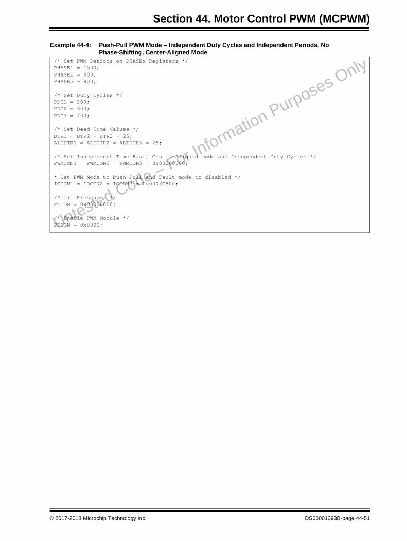
Section 44. Motor Control PWM (MCPWM)
Example 44-4: Push-Pull PWM Mode – Independent Duty Cycles and Independent Periods, No Phase-Shifting, Center-Aligned Mode
Untested Code – For Information Purposes Only
/* Set PWM Periods on PHASEx Registers */PHASE1 = 1000;PHASE2 = 900;PHASE3 = 800;
/* Set Duty Cycles */PDC1 = 200;PDC2 = 300;PDC3 = 400;
/* Set Dead Time Values */DTR1 = DTR2 = DTR3 = 25;ALTDTR1 = ALTDTR2 = ALTDTR3 = 25;
/* Set Independent Time Base, Center-Aligned mode and Independent Duty Cycles */PWMCON1 = PWMCON2 = PWMCON3 = 0x00000600;
* Set PWM Mode to Push-Pull and Fault mode to disabled */IOCON1 = IOCON2 = IOCON3 = 0x0003C800;
/* 1:1 Prescaler */PTCON = 0x00000000;
/* Enable PWM Module */PTCON = 0x8000;
© 2017-2018 Microchip Technology Inc. DS60001393B-page 44-51

PIC32 Family Reference Manual
44.7.2 Complementary PWM Mode
In Complementary PWM mode, the PWM output PWMxH is the complement of the PWMxLoutput. Some typical applications of Complementary PWM mode are providedin 44.20 “Application Information”.
Figure 44-8 through Figure 44-10 and Example 44-5 through Example 44-7 show the PWMoutputs in different commonly used configuration in Complementary PWM mode.
Figure 44-8: Complementary PWM Mode – Independent Duty Cycle and Phase, Fixed Period, Edge-Aligned
Note: Not all of the features and registers listed in the Figures and Code Examples in thissection are available on all devices. Refer to the “Motor Control PWM (MCPWM)”chapter in the specific device data sheet for availability.
PTPER
PHASE2PHASE3
PDC1
PDC2
PDC3
PWM1H
PWM1L
PWM2H
PWM2L
PWM3H
PWM3L
Start of PWM Cycle
Where,
PHASEx = Phase of PWMxH and PWMxL
PDCx = Duty Cycle of PWMxH and PWMxL
PTPER/STPER = Period of PWMxH and PWMxL
DTRx = Dead time for PWMxH Active Edge
ALTDTRx = Dead time for PWMxL Active Edge
DTR1
DTR2
DTR3
ALTDTR1
ALTDTR2
ALTDTR3PHASE1
DS60001393B-page 44-52 © 2017-2018 Microchip Technology Inc.
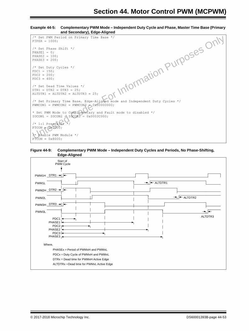
Section 44. Motor Control PWM (MCPWM)
Example 44-5: Complementary PWM Mode – Independent Duty Cycle and Phase, Master Time Base (Primary and Secondary), Edge-Aligned
Figure 44-9: Complementary PWM Mode – Independent Duty Cycles and Periods, No Phase-Shifting, Edge-Aligned
Untested Code – For Information Purposes Only
/* Set PWM Period on Primary Time Base */PTPER = 1000;
/* Set Phase Shift */PHASE1 = 0;PHASE2 = 100;PHASE3 = 200;
/* Set Duty Cycles */PDC1 = 150;PDC2 = 200;PDC3 = 400;
/* Set Dead Time Values */DTR1 = DTR2 = DTR3 = 25;ALTDTR1 = ALTDTR2 = ALTDTR3 = 25;
/* Set Primary Time Base, Edge-Aligned mode and Independent Duty Cycles */PWMCON1 = PWMCON2 = PWMCON3 = 0x00000000;
* Set PWM Mode to Complimentary and Fault mode to disabled */IOCON1 = IOCON2 = IOCON3 = 0x0003C000;
/* 1:1 Prescaler */PTCON = 0x0000;
/* Enable PWM Module */PTCON = 0x8000;
PWM1H
PWM1L
PWM2H
PWM2L
PWM3H
PWM3L
PDC1
PDC2
PDC3
PHASE1
PHASE2
PHASE3
Start of PWM Cycle
DTR1
DTR2
DTR3
ALTDTR1
ALTDTR2
ALTDTR3
Where,
PHASEx = Period of PWMxH and PWMxL
PDCx = Duty Cycle of PWMxH and PWMxL
DTRx = Dead time for PWMxH Active Edge
ALTDTRx = Dead time for PWMxL Active Edge
© 2017-2018 Microchip Technology Inc. DS60001393B-page 44-53

PIC32 Family Reference Manual
Example 44-6: Complementary PWM Mode – Independent Duty Cycles and Independent Periods, No Phase-Shifting, Edge-Aligned
Figure 44-10: Complementary PWM Mode – Independent Duty Cycles and Periods, No Phase-Shifting, Center-Aligned
Untested Code – For Information Purposes Only
/* Set PWM Periods on PHASEx Registers */PHASE1 = 800;PHASE2 = 900;PHASE3 = 1000;
/* Set Duty Cycles */PDC1 = 200;PDC2 = 300;PDC3 = 400;
/* Set Dead Time Values */DTR1 = DTR2 = DTR3 = 25;ALTDTR1 = ALTDTR2 = ALTDTR3 = 25;
/* Set Independent Time Base, Edge-Aligned mode and Independent Duty Cycles */PWMCON1 = PWMCON2 = PWMCON3 = 0x00000200;
* Set PWM Mode to Complimentary and Fault mode to disabled */IOCON1 = IOCON2 = IOCON3 = 0x0003C000;
/* 1:1 Prescaler */PTCON = 0x0000;
/* Enable PWM Module */PTCON = 0x8000;
DTR1
DTR2
DTR3
ALTDTR1
ALTDTR2
PWM1H
PDC1
PDC2
PDC3
Start of PWMCycle
PWM1L
PWM2H
ALTDTR3
PWM2L
PWM3L
PWM3H DTR3
PDC3 ALTDTR3
DTR3
PDC3 ALTDTR3
DTR2
ALTDTR2PDC2
DTR2
ALTDTR2PDC2
DTR1
ALTDTR1PDC1
PWM2H and PWM2L Cycle
PWM3H and PWM3L Cycle
PHASE1
PHASE2
PHASE3
Where:PHASEx = Half period of PWMxPDCx = Duty cycle of PWMxDTRx = Dead time for PWMxHALTDTRx = Dead time for PWMxL
PWM1H and PWM1L Cycle
DS60001393B-page 44-54 © 2017-2018 Microchip Technology Inc.

Section 44. Motor Control PWM (MCPWM)
Example 44-7: Complementary PWM Mode – Independent Duty Cycles and Independent Periods, No Phase-Shifting, Center-Aligned
Untested Code – For Information Purposes Only/* Set PWM Periods on PHASEx Registers */
PHASE1 = 1000;PHASE2 = 900;PHASE3 = 800;
/* Set Duty Cycles */PDC1 = 400;PDC2 = 300;PDC3 = 200;
/* Set Dead Time Values */DTR1 = DTR2 = DTR3 = 25;ALTDTR1 = ALTDTR2 = ALTDTR3 = 25;
/* Set Independent Base, Center-Aligned mode and Independent Duty Cycles */PWMCON1 = PWMCON2 = PWMCON3 = 0x00000600;
* Set PWM Mode to Complimentary and Fault mode to disabled */IOCON1 = IOCON2 = IOCON3 = 0x0003C000;
/* 1:1 Prescaler */PTCON = 0x0000;
/* Enable PWM Module */PTCON = 0x8000;
© 2017-2018 Microchip Technology Inc. DS60001393B-page 44-55

PIC32 Family Reference Manual
44.7.3 Redundant PWM Output Mode
In Redundant PWM Output mode, the MCPWM module can provide two copies of a single-endedPWM output signal per PWM pin pair (PWMxH, PWMxL). This mode uses the PWM GeneratedDuty Cycle register (PDCx) to specify the duty cycle. In this output mode, the two PWM outputpins will provide the same PWM signal unless the user-assigned application specifies an overridevalue through the OVRENH, OVRENL, and OVRDAT<1:0> bits in the IOCONx register togenerate waveforms for specific applications, such as switched reluctance motors. Dead timegeneration and compensation have no effect in this mode. Figure 44-11, Example 44-8,Figure 44-12, and Example 44-9 show the Redundant PWM Output mode in some commonlyused configurations.
Figure 44-11: Redundant PWM Mode – Independent Duty Cycle and Phase, Fixed Period, Edge-Aligned
Note: Not all of the features and registers listed in the Figures and Code Examples in thissection are available on all devices. Refer to the “Motor Control PWM (MCPWM)”chapter in the specific device data sheet for availability.
PTPER
PHASE1PHASE2PHASE3
PDC1
PDC2
PDC3
PWM1H
PWM1L
PWM2H
PWM2L
PWM3H
PWM3L
Start of PWM Cycle
Where,
PHASEx = Phase of PWMxH and PWMxL
PDCx = Duty Cycle of PWMxH and PWMxL
PTPER/STPER = Period of PWMxH and PWMxL
DS60001393B-page 44-56 © 2017-2018 Microchip Technology Inc.

Section 44. Motor Control PWM (MCPWM)
Example 44-8: Redundant PWM Mode – Independent Duty Cycle and Phase, Edge-Aligned
Figure 44-12: Redundant PWM Mode – Independent Duty Cycles and Periods, No Phase-Shifting, Edge-Aligned
Untested Code – For Information Purposes Only/* Set PWM Period on Primary Time Base */
PTPER = 1000;
/* Set Phase Shift */PHASE1 = 0;PHASE2 = 100;PHASE3 = 200;
/* Set Duty Cycles */PDC1 = 150;PDC2 = 200;PDC3 = 400;
/* Set Dead Time Values */DTR1 = DTR2 = DTR3 = 0;ALTDTR1 = ALTDTR2 = ALTDTR3 = 0;
/* Set Primary Time Base, Edge-Aligned mode and Independent Duty Cycles */PWMCON1 = PWMCON2 = PWMCON3 = 0x00000000;
* Set PWM Mode to Redundant and Fault mode to disabled */IOCON1 = IOCON2 = IOCON3 = 0x0003C400;
/* 1:1 Prescaler */PTCON = 0x0000;
/* Enable PWM Module */PTCON = 0x8000;
PWM1H
PWM1L
PWM2H
PWM2L
PWM3H
PWM3L
PDC1
PDC2
PDC3
PHASE1
PHASE2
PHASE3
Start of PWM Cycle
Where,
PHASEx = Period of PWMxH and PWMxL
PDCx = Duty Cycle of PWMxH and PWMxL
© 2017-2018 Microchip Technology Inc. DS60001393B-page 44-57

PIC32 Family Reference Manual
Example 44-9: Redundant PWM Mode – Independent Duty Cycles and Independent Periods, No Phase-Shifting
Table 44-5 provides PWM register functionality for the PWM modes.
Table 44-5: Complementary, Push-Pull and Redundant Mode Register Functionality
Untested Code – For Information Purposes Only/* Set PWM Periods on PHASEx Registers */
PHASE1 = 800;PHASE2 = 900;PHASE3 = 1000;
/* Set Duty Cycles */PDC1 = 200;PDC2 = 300;PDC3 = 400;
/* Set Dead Time Values */DTR1 = DTR2 = DTR3 = 0;ALTDTR1 = ALTDTR2 = ALTDTR3 = 0;
/* Set Independent Time Base, Edge-Aligned mode and Independent Duty Cycles */PWMCON1 = PWMCON2 = PWMCON3 = 0x00000200;
* Set PWM Mode to Redundant and Fault mode to disabled */IOCON1 = IOCON2 = IOCON3 = 0x0003C400;
/* 1:1 Prescaler */PTCON = 0x0000;
/* Enable PWM Module */PTCON = 0x8000;
FunctionConfiguration in PWMCONx
RegisterITB MTBS ECAM<1:0>
Duty Cycle x x 00, 01 PDCx
x x 10, 11 PDCx/SDCx
Phase Shift 0 x xx PHASEx
Period 0 0 xx PTPER
0 1 xx STPER
1 x xx PHASEx
Legend: x = don’t care
DS60001393B-page 44-58 © 2017-2018 Microchip Technology Inc.

Section 44. Motor Control PWM (MCPWM)
44.7.4 True Independent Output Mode
The MCPWM module does not support true independent mode in hardware. However, twoPWMxH pins of two separate generators can be synchronized with a common master time basewith same results (see Note).
The two PWMxH pins can be enabled through re programmable logic using PWM alternate I/OPin Select Bits CFGCON<23:18> for true independent mode function.
Example 44-10 shows the true independent function realized with two PWMxH pins of separategenerators with dead time disabled, synchronized to the same master time base, and thePHASEx registers providing the relative offset between the waveforms.
Example 44-10: PWM Channels Configured for True Independent Operation
Note: This feature is only supported on devices where the PWMxH and PWMxL of differ-ent generators are multiplexed to the same pin. This is a device specific feature andis not always available on all devices. Refer to the “Motor Control PWM(MCPWM)” chapter in the specific device data sheet for details regarding supportfor this mode.
Untested Code – For In
formation Purposes O
nly/* Set PWM Period on Primary Time Base */PTPER = 1000;
/* Set relative offsets between the PWM waveforms to PERIOD/2 */PHASE1 = 0;PHASE7 = 500; /* One-half of PWM period */
/* Set Symmetric Duty Cycles */PDC1 = 300;PDC7 = 300;
/* Set Dead time control to disabled and Edge-Aligned mode enabled */PWMCON1 = PWMCON7 = 0x00000080;
/* Set PWM mode to Redundant output mode and fault mode to disabled*//* Set PWMxL to I/O Function */IOCON1 = IOCON7 = 0x00038400;
/* Write Unlock Sequence to allow write access to CFGCON register */ SYSKEY = 0xAA996655; SYSKEY = 0x556699AA; /*Remap PWM7H to PWM1L*/ CFGCONbits.PWMAPIN1=1;/*Lock Write access to CFGCON register */SYSKEY = 0;
/* Set Primary Time Base*//* 1:1 Prescaler */PTCON = 0x0000;
/* Enable PWM Module */PTCON = 0x8000;
© 2017-2018 Microchip Technology Inc. DS60001393B-page 44-59

PIC32 Family Reference Manual
Figure 44-13: True Independent PWM Mode - Independent Duty Cycle, Fixed Period, Phase Shifting, Edge-Aligned
DS60001393B-page 44-60 © 2017-2018 Microchip Technology Inc.

Section 44. Motor Control PWM (MCPWM)
44.8 PWM GENERATION
This section describes the functionality of the PWM generator.
44.8.1 PWM Period
The PWM period value defines the switching frequency of the PWM pulses. The PWM periodvalue can be controlled by the PTPER/STPER register, or by the Independent Time Periodregister, PHASEx, for the primary and secondary PWM outputs.
The PWM period value can be controlled in two ways
• When running the PWM generators in the PWM Master Time Base mode (ITB bit (PWMCONx<9>) = 0) the period depends on the PTPER (MTBS bit (PWMCONx<3>) = 0) or the STPER registers (MTBS = 1)
• When in the Independent Time Base mode (ITB = 1) the period depends on the PHASEx register
For detailed information about various PWM modes and their features, refer to 44.7 “PWMOperating Modes”.
When the MCPWM module operates in Master Time Base mode, the PTPER register holdsthe 16-bit value, which specifies the counting period for the primary master time base timer.When the MCPWM module operates in Independent Time Base mode, the PHASEx registerholds the 16-bit value that specifies the counting period for the PTMRx timer. The timer periodcan be updated at any time by the user-assigned application. The PWM time period(PTPER/STPER/PHASEx) in Edge-Aligned PWM mode (ECAM bit PWMCONx<11:10> = 0b00)is set to ‘0’ can be determined using Equation 44-1.
Equation 44-1: Period Register Value Calculation for Edge-Aligned Mode
While operating in the primary/secondary master time base (i.e., ITB bit (PWMCONx<9>) = 0),the period value is loaded in the PTPER/STPER registers, respectively. While operating inindependent time base (PHASEx register) (i.e., ITB bit (PWMCONx<9>) = 1), the period value isloaded in the PHASEx register. Based on Equation 44-1, the value to be loaded is shown in.Equation 44-2.
Equation 44-2: Period Register Value Calculation for Edge-Aligned Mode
Note: Not all registers and features listed in this section are available on all devices. Referto the “Motor Control PWM (MCPWM)” chapter in the specific device data sheetfor availability.
Where,
FPWM = Desired PWM frequency
FSYSCLK = System Clock Frequency
PWM Input Clock Prescaler = Value defined in the PCLKDIV<2:0> bits (PTCON<6:4>),SCLKDIV<2:0> bits (STCON<6:4>)
PTPER STPER PHASEx FSYSCLKFPWM PWMInputClockPrescaler--------------------------------------------------------------------------------------------=
PTPER STPER PHASEx 120MHz20kHz 1------------------------- 6000= =
Where,
20 kHz = Desired PWM Switching Frequency
1:1 = PWM Input Clock Prescaler
120 MHz = System Clock (FSYSCLK)
© 2017-2018 Microchip Technology Inc. DS60001393B-page 44-61

PIC32 Family Reference Manual
The PWM time period (PTPER/STPER/PHASEx) in Center-Aligned mode (ECAM bit(PWMCONx<11:10>=01,10,11)) can be determined using Equation 44-3.
Equation 44-3: Period Register Value Calculation in Center-Aligned Mode
While operating in the primary/secondary master time base, (i.e., ITB bit (PWMCONx<9>) = 0),the period value is loaded in PTPER/STPER registers respectively. While operating inindependent time base (PHASEx register) (i.e., ITB bit (PWMCONx<9>) = 1), the period value isloaded in PHASEx register. Based on Equation 44-3, the value to be loaded is shown inEquation 44-4.
Equation 44-4: Period Register Value Calculation in Center-Aligned Mode
The maximum available PWM period resolution is 1/FSYSCLK for Edge-Aligned mode and 1/2 *FSYSCLK in Center-Aligned mode. The PCLKDIV<2:0> bits (PTCON<6:4>) and SCLKDIV<2:0>bits (STCON<6:4>), prescales the PWM clock. The timer or counter is enabled or disabled bysetting or clearing the PWM Module Enable bit, PTEN (PTCON<15>). The primary master timebase timer can also be cleared by clearing the PTEN bit. Example 44-11 provides the code forclock prescaler selection. Example 44-12 provides the code for PWM time period selection.Example 44-13 provides the code for PWM time period initialization.
Example 44-11: Clock Prescaler Selection
Example 44-12: PWM Time Period Selection
Example 44-13: PWM Time Period Initialization
PTPER STPER PHASEx FSYSCLKFPWM PWM Input Clock Prescaler 2---------------------------------------------------------------------------------------------------=
Where,
FSYSCLK = System Clock frequency
FPWM = Desired PWM frequency
PTPER STPER PHASEx 120MHz20 kHz 1 2----------------------------------- 3000==
Where,
PWM Frequency (FPWM) = 20 kHz
PWM Input Clock Prescaler = 1:1
System Clock Frequency (FSYSCLK) = 120 MHz
/* Select PWM time base input clock prescaler *//* Choose divide ratio of 1:2 */
PTCONbits.PCLKDIV = 1;
Untested Code – For Information Purposes Only
/* Select Time Base Period Control *//* Choose one of these options */
PWMCON1bits.ITB = 0; /* PTPER provides the PWM time period value */PWMCON1bits.ITB = 1; /* PHASEx/SPHASEx provides the PWM time period value */Untested Code – For Information Purposes Only
Untested Code – For Information Purposes Only/* PWM frequency is 20 kHz *//* Choose one of the following options */
PTPER = 2000;
PHASEx = 2000;
DS60001393B-page 44-62 © 2017-2018 Microchip Technology Inc.

Section 44. Motor Control PWM (MCPWM)
44.8.2 PWM Duty Cycle
They duty cycle of the PWMxH and PWMxL outputs is determined by the values in the PDCx andSDCx registers. The function of these registers varies with the PWM operating mode.
• Edge Aligned Mode: The PDCx register determines the PWM duty cycle
• Center-Aligned Mode: In this mode, the values written to the PDCx register is copied to SDCx register. The PDCx and SDCx registers store the compare value to match against the local timer (PTMRx).
• Asymmetric Center-Aligned Mode: In this mode, different values are written separately to the PDCx and SDCx registers. The PDCx value decides the edge transition when PTDIR = 1 and the SDCx value decides the edge transition when PTDIR = 0.
The duty cycle can be determined using Equation 44-5 through Equation 44-7 for the differentalignment modes.
Equation 44-5: PDCx Calculation for Edge-Aligned Mode
Equation 44-6: PDCx Calculations for Center-Aligned Mode
Equation 44-7: PDCx and SDCx Calculations for Asymmetric Center-Aligned Mode
Note 1: If a duty cycle value is greater than or equal to the period value, PWMxH will havea 100% duty cycle and PWMxL will have a 0% duty cycle.
2: If the duty cycle value is specified to be zero, PWMxH will have a 0% duty cycle andPWMxL will have a 100% duty cycle.
3: If the PDCx > DTRx condition is not satisfied, this could result in PWMxH being heldconstantly low.
PDCx FSYSCLKFPWM PWM Input Clock Prescaler------------------------------------------------------------------------------------------ DesiredDutyCycle=
Where,
FPWM = PWM Frequency
PWM Input Clock Prescaler = Value defined in the PCLKDIV<2:0> bits (PTCON<6:4>),SCLKDIV<2:0> bits (STCON<6:4>)
Desired Duty Cycle = Value between 0 and 1 for the desired duty cycle
PDCx FSYSCLK Desired Duty Cycle FPWM 2 PWM Input Clock Prescaler ----------------------------------------------------------------------------------------------------=
Where,
FPWM = PWM Frequency
PWM Input Clock Prescaler = Value defined in the PCLKDIV<2:0> bits (PTCON<6:4>),SCLKDIV<2:0> bits (STCON<6:4>)
Desired Duty Cycle = Value between 0 and 1 for the desired duty cycle
PDCx FSYSCLK Duty Cycle 1 FPWM 2 PWM Input Clock Prescaler ----------------------------------------------------------------------------------------------------=
Where,
FPWM = PWM Frequency
PWM Input Clock Prescaler = Value defined in the PCLKDIV<2:0> bits (PTCON<6:4>),SCLKDIV<2:0> bits (STCON<6:4>)
Duty Cycle ‘x’ = Value between 0 and 1
SDCx FSYSCLK Duty Cycle 2 FPWM 2 PWM Input Clock Prescaler ----------------------------------------------------------------------------------------------------=
© 2017-2018 Microchip Technology Inc. DS60001393B-page 44-63

PIC32 Family Reference Manual
44.8.2.1 DUTY CYCLE RESOLUTION
The PWM duty cycle bit resolution for Edge-Aligned mode can be determined usingEquation 44-8, and the PWM duty cycle bit resolution for Center-Aligned mode can bedetermined using Equation 44-9. Example 44-14 provides the code for PWM duty cycleinitialization.
Equation 44-8: Bit Resolution Calculation for Edge-Aligned Mode
Equation 44-9: Bit Resolution Calculation for Center-Aligned Mode
Example 44-14: PWM Duty Cycle Initialization
44.8.2.2 DUTY CYCLE LIMITS
In the Center-Aligned and Edge-Aligned modes for a PDCx value of ‘0’ the output is held at adeasserted state, which corresponds to a duty cycle of 0%. Similarly, for a PDCx value equal toor greater than the Period (PTPER,STPER or PHASEx) register, the output is held at an assertedstate, which corresponds to a duty cycle of 100%.
In the asymmetric Center-Aligned modes both the PDCx and SDCx registers will have to bewritten with 0 or PERIOD values in order to generate 0% and 100% duty cycles.
Bit Resolution 2FSYSCLK
FPWM PWM Input Clock Prescaler------------------------------------------------------------------------------------------log=
Bit Resolution 2FSYSCLK
FPWM PWM Input Clock Prescaler 2---------------------------------------------------------------------------------------------------log=Untested Code – For Information Purposes Only
/*Initialize PWM Period Value*/PTPER = 2000;/* Initialize PWM Duty Cycle Value */
PDC1 = 1000; /* Duty Cycle is 50% of the period */
DS60001393B-page 44-64 © 2017-2018 Microchip Technology Inc.

Section 44. Motor Control PWM (MCPWM)
44.8.3 Dead Time Generation
The dead time refers to a programmable period of time (specified by the PWM Dead Timeregister (DTRx) or the PWM Alternate Dead Time register (ALTDTRx)), which prevents a PWMoutput from being asserted until its complementary PWM signal has been deasserted for thespecified time.
The dead time registers can specify a total duration of 16384 multiplied by FSYSCLK. Powerdevices often have asymmetric turn-on and turn-off times requiring separate dead time registersfor the different devices coming into and going out of conduction.
44.8.3.1 DEAD TIME MODES
The following are three Dead Time Control modes:
• Positive Dead Time
• Negative Dead Time
• Dead Time Disabled
The dead time can be determined using the formula shown in Equation 44-10.
Equation 44-10: Dead Time Calculation
44.8.3.2 POSITIVE DEAD TIME
Positive Dead Time mode describes a period of time when both PWMxH and PWMxL outputsare not asserted. This mode is useful when active or synchronous rectification is desired tocontinue carrying the recirculation current. This is similar to a “Break before Make” switch. WhenPositive Dead Time mode is specified, the DTRx register specifies the dead time for the PWMxHoutput, and the ALTDTRx register specifies the dead time for the PWMxL output. This mode isillustrated in Figure 44-14 and Figure 44-15.
Using preprogrammed dead time delay values, positive dead time works by delaying the edgesof the PWM outputs that are in the process of going active. Positive dead time can be specifiedfor all complementary modes and are in effect even during the Fault, Current-Limit and themanually overridden states. Positive Dead times as a general rule are to be kept to a minimumto avoid over heating and harmonic distortion.
44.8.3.3 NEGATIVE DEAD TIME
The Negative Dead Time mode describes a period of time when both the PWMxH and PWMxLoutputs are asserted. This mode is useful in current-fed power conversion topologies that needto provide a path for current to flow when the power transistors are switching. This is similar to a“Make before Break” switch. When Negative Dead Time mode is specified, the DTRx registerspecifies the negative dead time for the PWMxH output, and the ALTDTRx register specifies thenegative dead time for the PWMxL output. Negative dead time is only supported in theedge-aligned mode. In the center-aligned mode, the negative dead time selection defeats thedead time generator.
Negative dead time is generated by delaying the edges that deassert the PWM to their inactivestates. Some power conversion techniques, such as current source inverters, require a limitedamount of current shoot through. Negative dead time is specified only for the Edge-Aligned PWMmode and does not affect the overridden output states of the PWMxH and PWMxL pins. Thismode is illustrated in Figure 44-14.
ALTDTRx DTRx FSYSCLK DesiredDeadTimePWMInputClockPrescaler-----------------------------------------------------------------------=
© 2017-2018 Microchip Technology Inc. DS60001393B-page 44-65
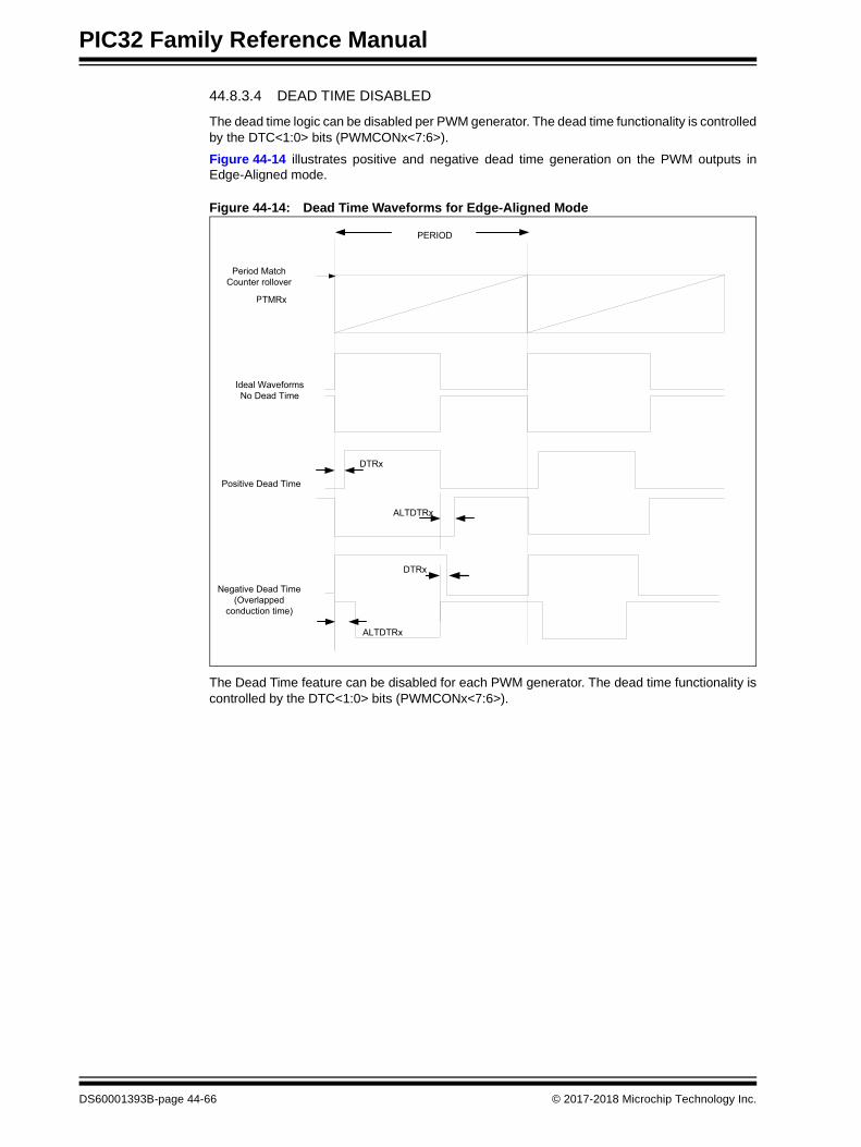
PIC32 Family Reference Manual
44.8.3.4 DEAD TIME DISABLED
The dead time logic can be disabled per PWM generator. The dead time functionality is controlledby the DTC<1:0> bits (PWMCONx<7:6>).
Figure 44-14 illustrates positive and negative dead time generation on the PWM outputs inEdge-Aligned mode.
Figure 44-14: Dead Time Waveforms for Edge-Aligned Mode
The Dead Time feature can be disabled for each PWM generator. The dead time functionality iscontrolled by the DTC<1:0> bits (PWMCONx<7:6>).
Negative Dead Time (Overlapped
conduction time)
PERIOD
DTRx
ALTDTRx
ALTDTRx
DTRx
Ideal WaveformsNo Dead Time
TMRx
Period MatchCounter rollover
Positive Dead Time
P
DS60001393B-page 44-66 © 2017-2018 Microchip Technology Inc.

Section 44. Motor Control PWM (MCPWM)
Figure 44-15 illustrates the positive dead time generation for Center-Aligned mode.
Figure 44-15: Dead Time Waveforms for Center-Aligned Mode
Positive Dead Time
PWM PERIOD
DTRx
ALTDTRx
TMRx
Ideal WaveformsNo Dead Time
Period Match
Timer Underflow
P
© 2017-2018 Microchip Technology Inc. DS60001393B-page 44-67

PIC32 Family Reference Manual
44.8.4 Dead Time Ranges
The dead time duration provided by each dead time unit is set by specifying an unsigned valuein the DTRx and ALTDTRx registers. At maximum operating clock frequency with a SYSCLK dutycycle resolution, the dead time resolution is SYSCK (8.33 ns at 120 MHz of SYSCLK). Themaximum dead time value is (214 – 1) SYSCLK = 136.52 µs when operating at 120 MHzSYSCLK.
44.8.5 Dead Time Distortion
For PDCx duty cycle values that are less than or equal to the DTRx register value, the PWMxHduty cycle is held at 0%; however, PWMxL is clamped to a duty cycle of Period - PDCx -ALTDTRx (Period is the value given by the PTPER, STPER, or PHASEx registers). Thiscondition is different from a PDCx = 0 specification when PWMxH shows a duty cycle of 0% andPWMxL shows a duty cycle of 100%. A similar situation exists when the PDCx duty cycle isgreater than or equal to Period minus the ALTDTRx register values, but is not equal to or abovethe Period value. This condition clamps PWMxH duty cycle to PDCx – DTRx and the PWMxL to0% duty cycle. This condition again is different from PDCx being greater than or equal to thePeriod value when the PWMxH is held at 100% duty cycle and PWMxL is held at 0% duty cycle.This behavior at duty cycle extremes, although a small portion of the controlled percentage, cancause distortion or a discontinuity in the otherwise linear duty cycle control. This non-linearityposes some challenges to the control loops and makes generation of some discontinuous PWMschemes difficult.
Distortion due to dead time does not only occur at the duty cycle extremes. Since dead timesreduce or increase conduction times, a volt second product (Volt * Second) imbalance is createdwith a full conduction cycle of the modulated waveform (inverter output fundamental), whichdepends on the direction of current flow. Refer to Figure 44-56 for distortion effects due to deadtimes. Dead time distortion effects are more pronounced when the duty cycle approaches deadtime values, since the lost conduction time becomes a bigger proportion of the total conductiontime.
Dead times are inevitable in real world inverters; however, the accompanying distortion can bemitigated to a large extent. Dead time compensation is a common technique that requires currentdirection information detected in hardware. The non-linearity in the PWM control manifests as acontrol disturbance and the control algorithms or loops try to annul the effects of this distortion toan extent where it is not significant enough to resort to other methods. To keep distortion low inthese applications and still keep the controlled parameters, such as rise time and settling timewithin specifications, the control duty cycle is kept away from venturing close to these extremescases, if possible. Not all applications will permit this work around. Dead time compensation withrun-time updates to dead time registers is the only way to restore full linearity, as described in44.8.6 “Dead Time Compensation”.
Figure 44-16 shows the effects of the two dead times at different times in the conduction cycleof the modulated voltage and the resulting current distortion. The power devices shown carrycurrents through different paths based on the flow direction as indicated by the arrows. When thecurrent flow direction through the H bridge is negative, ideally, current flows through the high sideduring durations ‘A’ and ‘B’ and no conduction must occur through the low side FET. The low sideshould begin conduction at time ‘D’, which is a dead time region that results in a current flowthrough the high side, and results in imposing VBUS instead of VSS resulting in volt seconddistortion of the waveform. A similar distortion is seen at the leading edge of conduction with apositive direction current flow. The distortion effects on the voltage and current waveforms areexaggerated for clarity.
DS60001393B-page 44-68 © 2017-2018 Microchip Technology Inc.

Section 44. Motor Control PWM (MCPWM)
Figure 44-16: Effects of Dead Time Distortion
Distorted Current
Distorted Voltage
A B
C D
E F G
I JH
+
-
Current
K
-
++
-
VGND
F
Distortion due to incorrect power device in conduction.
© 2017-2018 Microchip Technology Inc. DS60001393B-page 44-69

PIC32 Family Reference Manual
Table 44-6 shows the non-linear or abrupt transition of PWM duty cycles for different duty cycle(PDCx) specifications. The dead time registers can be written with progressively smaller valuesto regain the linearity, if desired. Doing so is not the same as dead time compensation, whichdepends on adjustments based on the current flow direction. Refer to 44.8.6 “Dead TimeCompensation” for more information.
Table 44-6: Duty Cycle Distortion and Relationship to Dead Time
PDCx SpecificationDuty Cycle
PWMxH PWMxL
0 0% 100%
Period 100% 0%
< DTRx 0% Period – PDCx – ALTDTRx
> Period – ALTDTRx) PDCx – DTRx 0%
DS60001393B-page 44-70 © 2017-2018 Microchip Technology Inc.

Section 44. Motor Control PWM (MCPWM)
44.8.6 Dead Time Compensation
When H bridges switch current through their power transistors dead times are inserted to preventa shoot through. This dead band needs to be generated with information regarding the directionof current through the half bridge. The traditional way of generating dead band/time is to delayrising edges to prevent a conduction overlap. This method affects the Voltage waveformadversely resulting in current distortion/harmonics when the dead times become significantfraction of the overall period. This is due to the fact that the free-wheeling diodes conduct only inone direction and therefore, depending on the current direction, the dead time results in lostconduction time.
The Dead time compensation in the MCPWM module recovers this lost conduction time byadding or subtracting the DTRx and ALTDTRx values depending on the current directionobtained through the DTCMPy pins (see Note). Each generator has a DTCMPy pin associatedwith it. Dead time distortion causes variations in generated torque in motor applications that canaffect the stability of the control system, and the performance of the motor, especially in the lowspeed and low torque regions of operation. The harmonic content adds to the total harmonicdistortion causing poorer power factors in high voltage machines.
Dead Time Compensation mode enables an external signal (DTCMPx) to modify the duty cycleto overcome motor current distortion caused by the dead time.
When Dead Time Compensation mode is selected through the Dead Time Control bits,DTC<1:0> (PWMCONx<7:6>), an external input signal, DTCMPx, will cause the value in theDTCOMPx register to be added to, or subtracted from, the duty cycle specified by thePDCx/SDCx registers.
Only a single (Dead time Compensation register (DTCOMPx) is provided. A fixed value equal toeither DTRx or ALTDTRx can be loaded into DTCOMPx register, but will not compensatecompletely when the two dead times are very different. For full compensation, the software canmonitor the DTCMPx line in software and alter the DTCOMPx register value accordingly asprovided in Table 44-7.
Table 44-7: Updates to DTCOMPx Register Value for Full Dead Time Compensation
Note: The DTCMPy pins are associated with the FLTx input pins and are shared by aGPIO pin. Refer to the specific device data sheets for the “x-y” correlation. All FLTxpins can therefore be polled for or controlled in software. When the TRISx pin isset, the status can be polled in software. When the TRISx pin is cleared, softwarecan assert/deassert status as desired. Care should be exercised when controllingthe Fault inputs in the user software. If the corresponding bit of the TRISx registerfor the Fault pin is cleared, the Fault input cannot be driven externally.
Polarity of DTCMPx Pin Logic Level at DTCMPx PinCompensation Value of
DTCOMPx Register
0 0 DTCOMPx = ALTDTRx
0 1 DTCOMPx = DTRx
1 0 DTCOMPx = DTRx
1 1 DTCOMPx = ALTDTRx
© 2017-2018 Microchip Technology Inc. DS60001393B-page 44-71

PIC32 Family Reference Manual
Figure 44-17 illustrates dead time compensation for PWM outputs in Edge-Aligned mode withpositive dead time configuration.
Figure 44-17: Edge-Aligned Positive Dead Time with Dead Time Compensation
DS60001393B-page 44-72 © 2017-2018 Microchip Technology Inc.
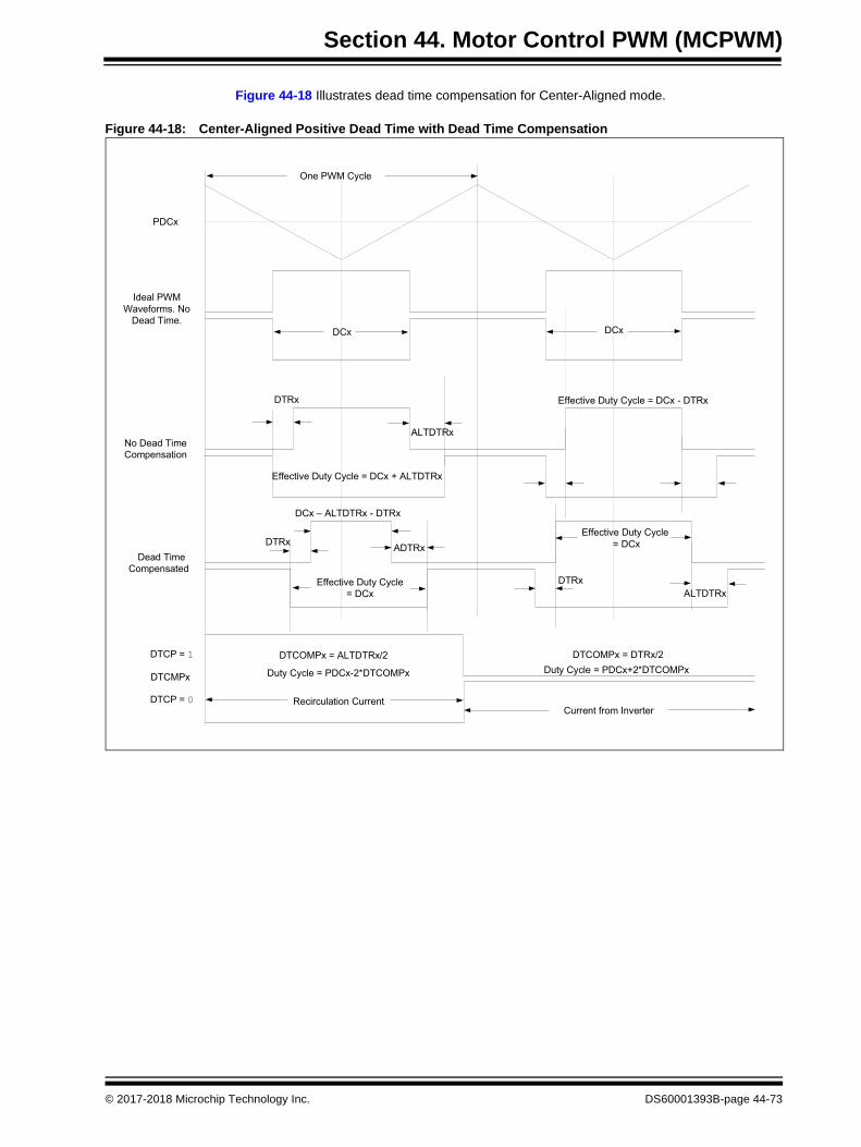
Section 44. Motor Control PWM (MCPWM)
Figure 44-18 Illustrates dead time compensation for Center-Aligned mode.
Figure 44-18: Center-Aligned Positive Dead Time with Dead Time Compensation
1
0
© 2017-2018 Microchip Technology Inc. DS60001393B-page 44-73

PIC32 Family Reference Manual
Table 44-8 and provides the rules for positive dead time compensation in Edge-Aligned andCenter-Aligned modes. Compensation rules do not apply for any mode that uses negative deadtime or Push-Pull mode.
Table 44-8: Dead Time Compensation Rules(1,2,3,4)
The dead time compensation external input control pin, DTCMPx, is sampled at the beginning ofeach dead time period. This ensures that the compensation is accurate to the maximum possibleextent. The DTCMPx pin determines whether the duty cycle will be increased or decreased bythe amount specified in the DTCOMPx register.
Pin in Edge-Aligned ModeDTCMPx = DTPOL,DTCOMPx = ALTDTRx
DTCMPx DTPOL,DTCOMPx = DTRx
PWMxH Duty Cycle PDCx – DTRx – DTCOMPx PDCx – DTRx + DTCOMPx
PWMxL Duty Cycle Period – (PDCx – DTCOMPx + ALTDTRx) Period – (PDCx + DTCOMPx + ALTDTRx)
Net effect on PWMxH Decrease Compensated = PDCx
Net effect on PWMxL Compensated = Period – PDCx Decrease
Pin in Center-Aligned ModeDTCMPx = DTPOLDTCOMPx = ALDTRx / 2
DTCMPx DTPOL,DTCOMPx = DTRx / 2
PWMxH Duty Cycle 2 * PDCx – DTRx – 2 * DTCOMPx 2 * PDCx – DTRx +2* DTCOMPx
PWMxL Duty Cycle Period – (2 * PDCx – 2 * DTCOMPx + ALTDTRx) Period – (2 * PDCx + 2 * DTCOMPx + ALT-DTRx)
Net effect on PWMxH Decrease Compensated = 2 * PDCx
Net effect on PWMxL Compensated = Period – 2 * PDCx Decrease
Note 1: Dead time compensation is not available for Negative Dead Time mode and Push-Pull mode.2: DTCMPx is a digital input pin.3: DTPOL is a SFR bit.4: DTCOMPx is the dead time compensation SFR.
Note 1: The DTCOMPx value must be less than one-half the value of the duty cycle (PDCx) register; otherwise, unpredictable behavior will result.
2: Dead time compensation will not apply for a duty cycle of 0%. In this case, the PWM output will remain 0% regardless of the state of the DTCMPx input pin.
DS60001393B-page 44-74 © 2017-2018 Microchip Technology Inc.

Section 44. Motor Control PWM (MCPWM)
44.8.7 Phase Shift
When the PWM generator is configured for synchronized operation, the phase shift value writtento the PHASEx register shifts both the PWMxH and PWMxL pins with respect to the master timebase.
For perfect synchronization between outputs of multiple generators, the phase shift registers(PHASEx) need to be updated to zero prior to enabling the MCPWM module (i.e., when thePTEN bit (PTCON<15>) = 0).
Figure 44-19 and Figure 44-20 illustrates two different PWM channel/generator outputs phaseshifted with respect to each other in Edge-Aligned and Center-Aligned modes, respectively.
Figure 44-19: Phase Shifting (Edge-Aligned Mode)
The phase offset value can be any value between zero and the value in the PTPER and STPERregisters. Any PHASEx value greater than the Period value will be treated as a value equal tothe Period. It is not possible to create phase shifts greater than the Period.
Master Time Base Timer
(PTMR/SMTMR)
PWM1 Local Timer(PTMR1)
PWM1H
PWM1L
PWM2 Local Timer
(PTMR2)
PWM2H
PWM2L
PHASEx = Phase Lag CountsPHASEx = Period – Phase Lead Counts
Period
Phase LagPTMR1 is Reset atPMTMR/SMTMR = 20
PTMR2 is Reset atPMTMR/SMTMR = 80
Phase Lead
STPER = 100PHASE2 = 80
PDCx = 50
PHASE1 = 20
PDC1 = 50
PDC2 = 50
PTPER/
Note: Phase lag and lead are with reference to the internal Master Time Base.
© 2017-2018 Microchip Technology Inc. DS60001393B-page 44-75

PIC32 Family Reference Manual
Figure 44-20: Phase Shift in Center-Aligned Mode
DS60001393B-page 44-76 © 2017-2018 Microchip Technology Inc.

Section 44. Motor Control PWM (MCPWM)
Figure 44-21 illustrates the effect of run-time updates to the PHASEx register of thechannel/generator timer in the synchronized modes.
Figure 44-21: Effect of Phase Shift on Channel/Generator Timer and Output Waveform
When phase shifting the PWM signal, the PWM timer value is updated to reflect the new phasevalue. There is a possibility of missing trigger events when changing the phase.Theuser-assigned application must ensure that this does not affect any control loop execution.
Write to PHASEx Register
PTPER/STPER = 100
Updated PHASEx Value
PDCx = 30
PDCx = 30
PWMxH
PWMxL
Master Time Base Timer(PMTMR/SMTMR)
PWMx Local Timer(PTMRx)
New value of PHASEx isupdated at Master Time Base Rollover
© 2017-2018 Microchip Technology Inc. DS60001393B-page 44-77
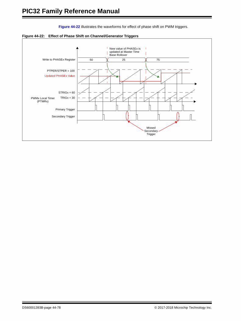
PIC32 Family Reference Manual
Figure 44-22 illustrates the waveforms for effect of phase shift on PWM triggers.
Figure 44-22: Effect of Phase Shift on Channel/Generator Triggers
Write to PHASEx Register
PTPER/STPER = 100
Updated PHASEx Value
STRIGx = 60
TRIGx = 30
Primary Trigger
Secondary Trigger
PWMx Local Timer(PTMRx)
New value of PHASEx isupdated at Master Time Base Rollover
50 25 75
MissedSecondary
Trigger
DS60001393B-page 44-78 © 2017-2018 Microchip Technology Inc.

Section 44. Motor Control PWM (MCPWM)
44.9 WRITE PROTECTION
Certain devices incorporate a write protection feature for the PWM I/O Control register(IOCONx), which prevents any inadvertent writes to these registers. This feature can becontrolled by the PWMLOCK Configuration bit (DEVCFG3<20>). The default state of the writeprotection feature is disabled (PWMLOCK = 1). Refer to the “Special Features” chapter in thespecific device data sheet for more information on Flash Configuration bytes.
To gain write access to the locked registers, the user application must write two consecutivevalues of 0xABCD and 0x4321 to the PWM Unlock register (PWMKEY). The write access to theIOCONx registers must be the next special function register (SFR) access following the unlocksequence; there can be no other SFR accesses during the unlock process and subsequent writeaccess.
The correct unlocking sequence is described in Example 44-15.
Example 44-15: PWM Write-Protected Register Unlock Sequence
Untested Code – For Information Purposes Only; FLT15 pin must be pulled high externally to clear and disable the fault; Writing to IOCONx register requires unlock sequencemov #0xabcd,r1 ;Load first unlock key to r1 registermov #0x4321,r2 ;Load second unlock key to r2 registermov r1, PWMKEY ;Write first unlock key to PWMKEY registermov r2, PWMKEY ;Write second unlock key to PWMKEY registermov r3,IOCON4 ;Write desired value to IOCON SFR for channel 4
© 2017-2018 Microchip Technology Inc. DS60001393B-page 44-79
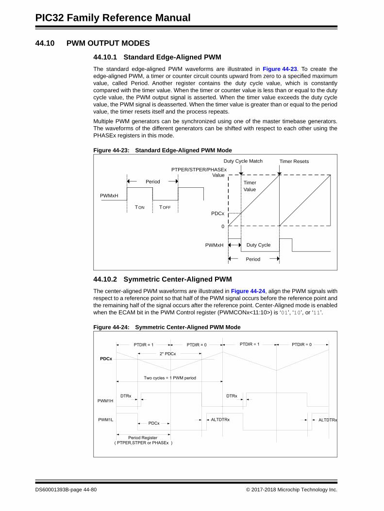
PIC32 Family Reference Manual
44.10 PWM OUTPUT MODES
44.10.1 Standard Edge-Aligned PWM
The standard edge-aligned PWM waveforms are illustrated in Figure 44-23. To create theedge-aligned PWM, a timer or counter circuit counts upward from zero to a specified maximumvalue, called Period. Another register contains the duty cycle value, which is constantlycompared with the timer value. When the timer or counter value is less than or equal to the dutycycle value, the PWM output signal is asserted. When the timer value exceeds the duty cyclevalue, the PWM signal is deasserted. When the timer value is greater than or equal to the periodvalue, the timer resets itself and the process repeats.
Multiple PWM generators can be synchronized using one of the master timebase generators.The waveforms of the different generators can be shifted with respect to each other using thePHASEx registers in this mode.
Figure 44-23: Standard Edge-Aligned PWM Mode
44.10.2 Symmetric Center-Aligned PWM
The center-aligned PWM waveforms are illustrated in Figure 44-24, align the PWM signals withrespect to a reference point so that half of the PWM signal occurs before the reference point andthe remaining half of the signal occurs after the reference point. Center-Aligned mode is enabledwhen the ECAM bit in the PWM Control register (PWMCONx<11:10>) is ‘01’, ‘10’, or ‘11’.
Figure 44-24: Symmetric Center-Aligned PWM Mode
PDCx
PTPER/STPER/PHASExValue
TimerValue
Duty Cycle Match Timer Resets
Period
Duty Cycle
0
Period
TOFFTON
PWMxH
PWMxH
DTRx
ALTDTRx
PWM1H
PDCxPWM1L
DTRx
ALTDTRx
Period Register ( PTPER,STPER or PHASEx )
TMRx
Two cycles = 1 PWM period
2* PDCx
PTDIR = 1 PTDIR = 0 PTDIR = 1 PTDIR = 0
PDCx
DS60001393B-page 44-80 © 2017-2018 Microchip Technology Inc.

Section 44. Motor Control PWM (MCPWM)
When operating in Center-Aligned mode, the effective PWM period is twice the value specifiedin the Period registers (PTPER/STPER/PHASEx), because the local timer (PTMRx) counter inthe PWM generator is counting up and then counting down during the cycle. The up/down countsequence doubles the effective PWM cycle period. This mode is used in many motor controlapplications.
The resolution of the PWM in the Center-Aligned mode is half that in the Edge-Aligned mode.When Center-Aligned mode with full resolution is desired, Asymmetric Center-Aligned mode isrecommended (ECAM<1:0> bits (PWMCONx<11:10>) = 10). The duty cycle registers PDCx andSDCx are written as follows to get full resolution:
• PDCx = Duty Cycle / 2
• SDCx = Duty Cycle - PDCx
An interrupt can also be generated at period match (PTMRx = PTPER/STPER/PHASEx). OnlyPDCx register is used in the Symmetric Center-Aligned PWM mode. The SDCx registerautomatically reflects the writes to the PDCx.
Figure 44-25 Illustrates the timing relationship between software updates to the PDCx (updatesto SDCx are transparent to software in this mode) registers and when the updates actually occurto the waveforms or pins.
Figure 44-25: Symmetric Mode Duty Cycle Update Timing Diagram
PTDIR
PMTMRSMTMR
TMR1
PDC1
TMR2
PDC2
PWM1
PWM2
PTPER/STPER
PTPER/STPER
20 50 10 90
10 70 70 50 50 25
0
0
PTPER/STPER
70 25
50 50
10
90 902020
10
1010
70 70 7025
Timer re-load PWM update
© 2017-2018 Microchip Technology Inc. DS60001393B-page 44-81

PIC32 Family Reference Manual
44.10.3 Asymmetric Center-Aligned PWM Mode
This mode is selected by setting the ECAM<1:0> bits (PWMCONx<11:10>) = 10. In this modethere are two duty cycle registers, PDCx and SDCx, that provide transition instances for theleading and trailing edges of the PWM. Effectively, the two registers permit users to generatesynchronous multiphase waveforms where the duty cycles are asymmetric about the internalsynchronizing reference. This mode is mainly used where asymmetric PWM schemes areutilized with a requirement for higher update bandwidth.
Figure 44-26 illustrates the asymmetric leading and trailing edge transitions about the centralreference unlike the Center-Aligned mode.
Figure 44-26: Asymmetric Center-Aligned PWM Mode
DS60001393B-page 44-82 © 2017-2018 Microchip Technology Inc.

Section 44. Motor Control PWM (MCPWM)
Figure 44-27 shows the timing relationship between software updates to the PDCx and SDCxregisters and when the updates actually occur on the waveforms/pins.
Figure 44-27: Asymmetric Mode Double Update Rate Timing Diagram
Example 44-16 shows how to configure the channel/generator in different alignment modes.
Example 44-16: Edge-Aligned or Center-Aligned Mode Selection
Untested Code – For Information Purposes Only/* Select Edge Aligned PWM mode */PWMCON1bits.ECAM = 0x00;
/* Select Center Aligned PWM mode */PWMCON1bits.ECAM = 0x01;
/* Select Asymmetric Center Aligned PWM mode with double update rate */PWMCON1bits.ECAM = 0x02;
/* Select Asymmetric Center Aligned PWM mode with simultaneous update */PWMCON1bits.ECAM = 0x03;
© 2017-2018 Microchip Technology Inc. DS60001393B-page 44-83

PIC32 Family Reference Manual
44.11 PWM GENERATOR TRIGGERS
The PWM module features ADC trigger outputs from each PWM generator. The trigger pulse canbe used to initiate a sample and conversion operation by the ADC or generate an interrupt.
Two compare registers, TRIGx and STRIGx are provided to facilitate triggering at specific pointsin time during the generation of the PWMxH/PWMxL waveforms. The user specifies a matchvalue in each to generate two different triggers at different points in the waveform within theperiod when the values match with the local timebase timer, PTMRx.
Some PWM modes, such as Center-Aligned mode and Push-Pull mode are two-cycle PWMcycles. The default trigger generation behavior is to create two raw trigger comparison eventsduring the two-cycle PWM cycle. The TRGSEL<1:0> bits (TRGCONx<11:0>) enable the user toselect both triggers or only the raw comparison event from the first or second half of the two-cyclePWM cycle.
The trigger pulses share a common PWM cycle divider, TRGDIV<3:0> bits (TRGCONx<15:12>).This allows the trigger signals to the ADC to be generated once for every 1, 2, 3-16 trigger events.
The trigger divider allows the user to tailor the ADC sample rates to the control looprequirements.
If the TRGIEN bit (PWMCONx<21>) is set to ‘1’ in the PWMCONx register, an interrupt requestis generated.
Figure 44-28 illustrates the three different triggering possibilities to the ADC module from theMCPWM module in conjunction with the associated interrupt capability.
Figure 44-28: PWM Trigger for Analog-to-Digital Conversion
Note 1: The trigger pulse for use as an ADC trigger is generated regardless of the state ofthe TRGIEN bit.
2: With two-cycle PWM modes, care should be taken to prevent back-to-backinterrupts that could occur at the higher or lower end of the Period values.
TRIGx
Local Timer TMRx
TRGDIV<3:0>
To PWM interrupt logic
1:1
1:16 PWMx Secondary Triggerto ADC
GatingLogic
GatingLogic
PWM Clock Primary or Secondary
Master Time base
TRGDIV<3:0>
TRGSEL<1:0>
STRGSEL<1:0>
0
1
STRGIS
PWMx Primary Trigger to ADC
DTMECAM<1:0> PTDIR
STRIGx
Comparator =
Comparator =
1:1
1:16
Local Timer PTMRx
Note: A trigger can only be generated on the first PWM interval when theTRGDIV<3:0> bits are set to ‘0’.
DS60001393B-page 44-84 © 2017-2018 Microchip Technology Inc.

Section 44. Motor Control PWM (MCPWM)
Depending on the settings of the TRGDIV<3:0> bits, triggers are generated at different PWMintervals, as illustrated in Figure 44-29 through Figure 44-32.
Figure 44-29: PWM Trigger Signal in Relation to the PWM Output in Edge-Aligned Mode (TRGDIV = 0)
Figure 44-30: PWM Trigger Signal in Relation to the PWM Output in Edge-Aligned Mode (TRGDIV = 1)
PWMxH
TRIGx = 0
TRIGx = 8
TRIGx = 4808
TRIGx = 9616
1
PTPER = 9616
62 3 4 5 7
PWMxH
TRIGx = 0
TRIGx = 8
TRIGx = 4808
TRIGx = 9616
PTPER = 9616
51 2 3 4 6
© 2017-2018 Microchip Technology Inc. DS60001393B-page 44-85

PIC32 Family Reference Manual
Figure 44-31: PWM Trigger Signal in Relation to the PWM Output in Edge-Aligned Mode (TRGDIV = 2)
Figure 44-32: Trigger Signal in Relation to PWM Output in Center-Aligned Mode (TRGDIV = 0, TRGSEL = 0 or 3)
Figure 44-33 illustrates the waveforms for trigger signal and scaling in relation to the PWMoutput in Center-Aligned mode (TRGDIV = 1).
Figure 44-33: Trigger Signal in Relation to PWM Output in Center-Aligned Mode (TRGDIV = 1, TRGSEL = 0 or 3)
PWMxH
TRIGx = 0
TRIGx = 8
TRIGx = 4808
TRIGx = 9616
1
PTPER = 9616
62 3 4 5 7
1 2PWMxH
TRIGx = 0
TRIGx = 500
TRIGx = 250
TRIGx = 750
TRIGx = 1000
PDCx = 500
3 4
1 2PWMxH
TRIGx = 0
TRIGx = 500
TRIGx = 250
TRIGx = 750
TRIGx = 1000
PDCx = 500
PHASEx = PTPER = 1000
3 4
DS60001393B-page 44-86 © 2017-2018 Microchip Technology Inc.

Section 44. Motor Control PWM (MCPWM)
Figure 44-34: Trigger Signal in Relation to PWM Output in Center-Aligned Mode (TRGDIV = 0, TRGSEL = 1)
Figure 44-35: Trigger Signal in Relation to PWM Output in Center-Aligned Mode (TRGDIV = 0, TRGSEL = 2)
Figure 44-36: Trigger Signal in Relation to PWM Output in Center-Aligned Mode (TRGDIV = 1, TRGSEL = 2)
1 2PWMxH
TRIGx = 0
TRIGx = 500
TRIGx = 250
TRIGx = 750
TRIGx = 1000
PDCx = 500
3 4
1 2PWMxH
TRIGx = 0
TRIGx = 500
TRIGx = 250
TRIGx = 750
TRIGx = 1000
PDCx = 500
3 4
1 2PWMxH
TRIGx = 0
TRIGx = 500
TRIGx = 250
TRIGx = 750
TRIGx = 1000
PDCx = 500
3 4
© 2017-2018 Microchip Technology Inc. DS60001393B-page 44-87

PIC32 Family Reference Manual
Figure 44-37: Trigger Signal in Relation to PWM Output in Center-Aligned Mode (TRGDIV = 1, TRGSEL = 1)
The trigger divider allows the user-assigned application to tailor the ADC sample rates to therequirements of the control loop.
If ADC triggers are generated at a rate faster than the rate that the ADC can process, theoperation may result in loss of some samples. However, the user-assigned application canensure that the time it provides is enough to complete an ADC operation within a single PWMcycle.
The trigger pulse is generated regardless of the state of the Trigger Interrupt Enable bit,TRGIEN (PWMCONx<21>). If the TRGIEN bit is set to ‘1’, an interrupt request (IRQ) isgenerated. Example 44-1 in 44.5.2.1 “Special Event Trigger” provides the code forindependent PWM ADC triggering.
1 2PWMxH
TRIGx = 0
TRIGx = 500
TRIGx = 250
TRIGx = 750
TRIGx = 1000
PDCx = 500
3 4
Note 1: The Trigger Interrupt Status bit, TRGSTAT (PWMCONx<13>), is only cleared byclearing the TRGIEN bit. It is not cleared automatically.
2: Dynamic triggering can show some advantages where multiple PWM channels areused in applications, such as IPFC and multi-phase buck regulators. The TRIGxvalues can be changed based on the PWM period, duty, load current, and so on.This is to ensure that the trigger points are separated from the rise and fallinstances of the PWM channel.
DS60001393B-page 44-88 © 2017-2018 Microchip Technology Inc.

Section 44. Motor Control PWM (MCPWM)
Table 44-9 provides a summary of the registers used as period and compare values for ADCtriggers and the associated interrupts originating from the MCPWM module.
Table 44-9: ADC Triggers and Synchronization Sources with Associated Interrupts
Example 44-17 shows code for the generation of two triggers to the ADC module per cycle of thePWM module of Generator 1. The primary trigger (TRIGx) triggers during the first half and thesecondary trigger (STRIGx) triggers during the second half. The dual trigger mode is enabledwith interrupts enabled for both triggers and the same interrupt vector. Since the events arestaggered in time, a single interrupt reduces an extra interrupt source without concern fornesting.
Example 44-17: Dual Staggered Trigger and Interrupt Generation
ADC Trigger
Event(1) Trigger Interrupt(3) Trigger Source
DTM = “don’t care”
STRGIS = 0DTM = 0
STRGIS = 0DTM = 1
STRGIS = 1DTM = “don’t
care”
ITB = 0MTBS = 0
ITB = 0MTBS = 1
ITB = 1MTBS =
“don’t care”
SEVT SEVT SEVT SEVT PTPER PTPER PTPER
SSEVT SSEVT SSEVT SSEVT STPER STPER STPER
TRIGx, STRIGx
TRIGxTRIGx, STRIGx
STRIGx PTPER STPER PHASEx
PWM Generator x Current-Limit
Current-Limit InterruptAsynchronous, external digital input
event-based or FLTy(2) pin
Note 1: The selection of the ADC trigger event from the MCPWM module is specified in the ADC module (STRGSRC<4:0> bits (ADCCON1<20:16>)) and is device-specific. Refer to the “ADC” chapter in the specific device data sheet for ADC trigger associations.
2: “x” and “y” = 1, up to 6. Refer to the specific device data sheet to determine availability and pin assignments.
3: There is only a single interrupt vector for both TRIGx and STRIGx interrupt sources. Software is required to arbitrate the source of the interrupt.
Untested Code – For Information Purposes OnlyTRGCON1bits.DTM = 1; // Logically OR the interrupt sources to the
// same vectorTRGCON1bits.STRGIS = 0; // Enable both interrupts TRGCON1bits.TRGDIV = 0; // No postscaler divider; trigger and interrupt
// every cycle TRGCON1bits.TRGSEL = 1; // Trigger only during the first half of the cycleTRGCON1bits.STRGDIV = 0; // No postscaler divider; trigger and interrupt
// every cycle TRGCON1bits.STRGSEL = 2; // Trigger only during the second half of the cycle
© 2017-2018 Microchip Technology Inc. DS60001393B-page 44-89

PIC32 Family Reference Manual
44.12 PWM INTERRUPTS
The MCPWM module can generate interrupts based on internal timing signals or external signalsthrough the current-limit and fault inputs. Each PWM generator module provides its own IRQsignal to the interrupt controller. The interrupt for each PWM generator is a Boolean OR of thetrigger event IRQ, period match, period Reset, current-limit input event, or fault input event forthat module.
Besides one IRQ signal per PWM generator, the interrupt controller receives an IRQ signal fromthe master time base on each of the two special events.
The IRQs coming from each PWM generator are called Individual PWM Interrupts. The IRQ foreach one of these individual interrupts can come from the PWM individual trigger, PWM periodmatch/Reset, PWM fault logic, or PWM current-limit logic. Each PWM generator has the PWMinterrupt flag in an IFSx register. When an IRQ is generated by any of the above sources, thePWM interrupt flag associated with the selected PWM generator is set.
If more than one IRQ source is enabled, the interrupt source is determined using theuser-assigned application by checking the TRGIF bit (PWMCONx<29>), PWML Interrupt Statusbit (PWMCONx<28>, PWMH Interrupt Status bit (PWMCONx<27>), the Fault Interrupt Status bit,FLTSTAT (PWMCONx<15>) and the Current-limit Interrupt Status bit,CLSTAT (PWMCONx<14>).
To configure interrupts, the application software should first clear the interrupt flags, enable theinterrupts (see Register 44-1, Register 44-5 and Register 44-11), and finally, enable the MCPWMmodule.
44.12.1 PWM Time Base Interrupts
In each PWM generator, the MCPWM module can generate interrupts based on the master timebase and/or the individual time base. The SEVTCMP/SSEVTCMP register specifies timer basedinterrupts for the primary time base, and the TRIGx/STRIGx registers specify timer basedinterrupts for the individual time bases.
The primary time base special event interrupt is enabled through the SEIEN bit (PTCON<11>)and the secondary time base special event interrupt through the SSEIEN bit (STCON<11>). Ineach PWM generator, the individual time base interrupts generated by the trigger logic arecontrolled by the TRGIEN bit (PWMCONx<21>).
Note: When an appropriate match condition occurs, the Special Event Trigger signal andthe individual PWM trigger pulses to the ADC are always generated regardless ofthe setting of their respective interrupt enable bits.
DS60001393B-page 44-90 © 2017-2018 Microchip Technology Inc.
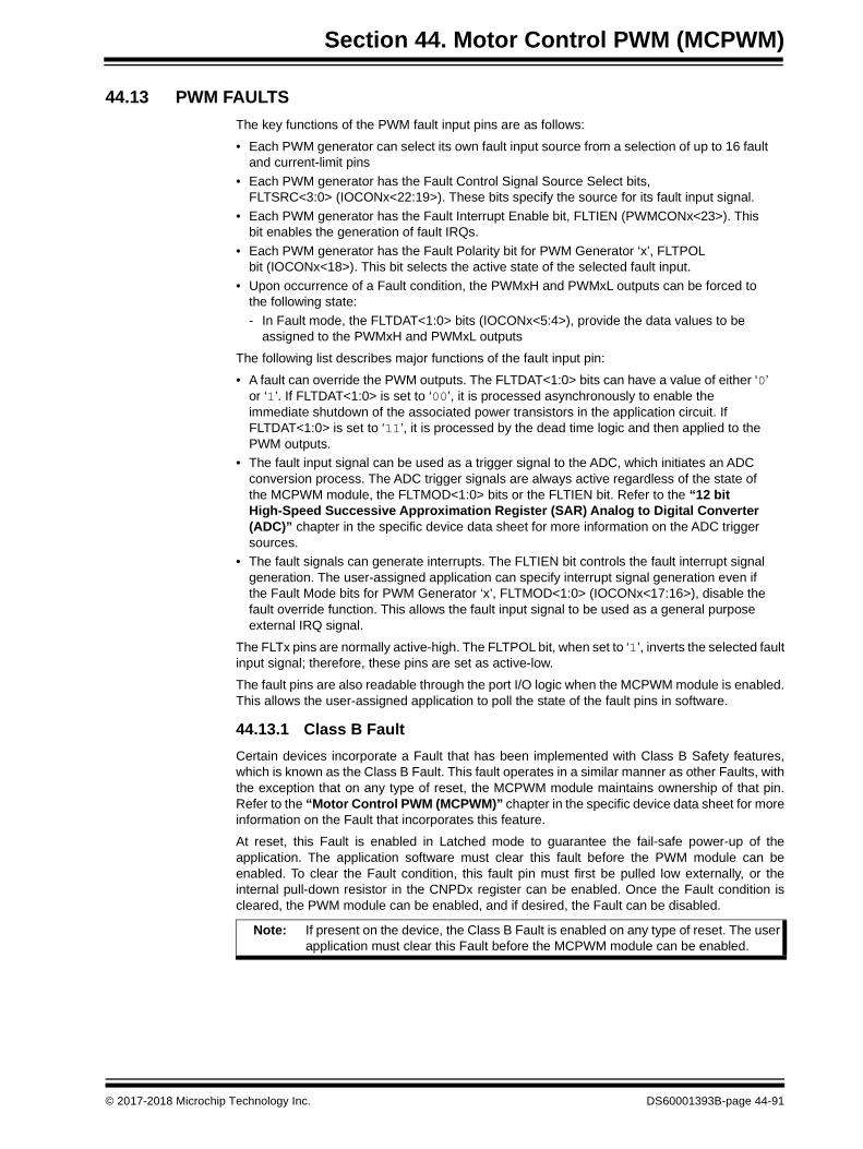
Section 44. Motor Control PWM (MCPWM)
44.13 PWM FAULTS
The key functions of the PWM fault input pins are as follows:
• Each PWM generator can select its own fault input source from a selection of up to 16 fault and current-limit pins
• Each PWM generator has the Fault Control Signal Source Select bits, FLTSRC<3:0> (IOCONx<22:19>). These bits specify the source for its fault input signal.
• Each PWM generator has the Fault Interrupt Enable bit, FLTIEN (PWMCONx<23>). This bit enables the generation of fault IRQs.
• Each PWM generator has the Fault Polarity bit for PWM Generator ‘x’, FLTPOL bit (IOCONx<18>). This bit selects the active state of the selected fault input.
• Upon occurrence of a Fault condition, the PWMxH and PWMxL outputs can be forced to the following state:
- In Fault mode, the FLTDAT<1:0> bits (IOCONx<5:4>), provide the data values to be assigned to the PWMxH and PWMxL outputs
The following list describes major functions of the fault input pin:
• A fault can override the PWM outputs. The FLTDAT<1:0> bits can have a value of either ‘0’ or ‘1’. If FLTDAT<1:0> is set to ‘00’, it is processed asynchronously to enable the immediate shutdown of the associated power transistors in the application circuit. If FLTDAT<1:0> is set to ‘11’, it is processed by the dead time logic and then applied to the PWM outputs.
• The fault input signal can be used as a trigger signal to the ADC, which initiates an ADC conversion process. The ADC trigger signals are always active regardless of the state of the MCPWM module, the FLTMOD<1:0> bits or the FLTIEN bit. Refer to the “12 bit High-Speed Successive Approximation Register (SAR) Analog to Digital Converter (ADC)” chapter in the specific device data sheet for more information on the ADC trigger sources.
• The fault signals can generate interrupts. The FLTIEN bit controls the fault interrupt signal generation. The user-assigned application can specify interrupt signal generation even if the Fault Mode bits for PWM Generator ‘x’, FLTMOD<1:0> (IOCONx<17:16>), disable the fault override function. This allows the fault input signal to be used as a general purpose external IRQ signal.
The FLTx pins are normally active-high. The FLTPOL bit, when set to ‘1’, inverts the selected faultinput signal; therefore, these pins are set as active-low.
The fault pins are also readable through the port I/O logic when the MCPWM module is enabled.This allows the user-assigned application to poll the state of the fault pins in software.
44.13.1 Class B Fault
Certain devices incorporate a Fault that has been implemented with Class B Safety features,which is known as the Class B Fault. This fault operates in a similar manner as other Faults, withthe exception that on any type of reset, the MCPWM module maintains ownership of that pin.Refer to the “Motor Control PWM (MCPWM)” chapter in the specific device data sheet for moreinformation on the Fault that incorporates this feature.
At reset, this Fault is enabled in Latched mode to guarantee the fail-safe power-up of theapplication. The application software must clear this fault before the PWM module can beenabled. To clear the Fault condition, this fault pin must first be pulled low externally, or theinternal pull-down resistor in the CNPDx register can be enabled. Once the Fault condition iscleared, the PWM module can be enabled, and if desired, the Fault can be disabled.
Note: If present on the device, the Class B Fault is enabled on any type of reset. The userapplication must clear this Fault before the MCPWM module can be enabled.
© 2017-2018 Microchip Technology Inc. DS60001393B-page 44-91
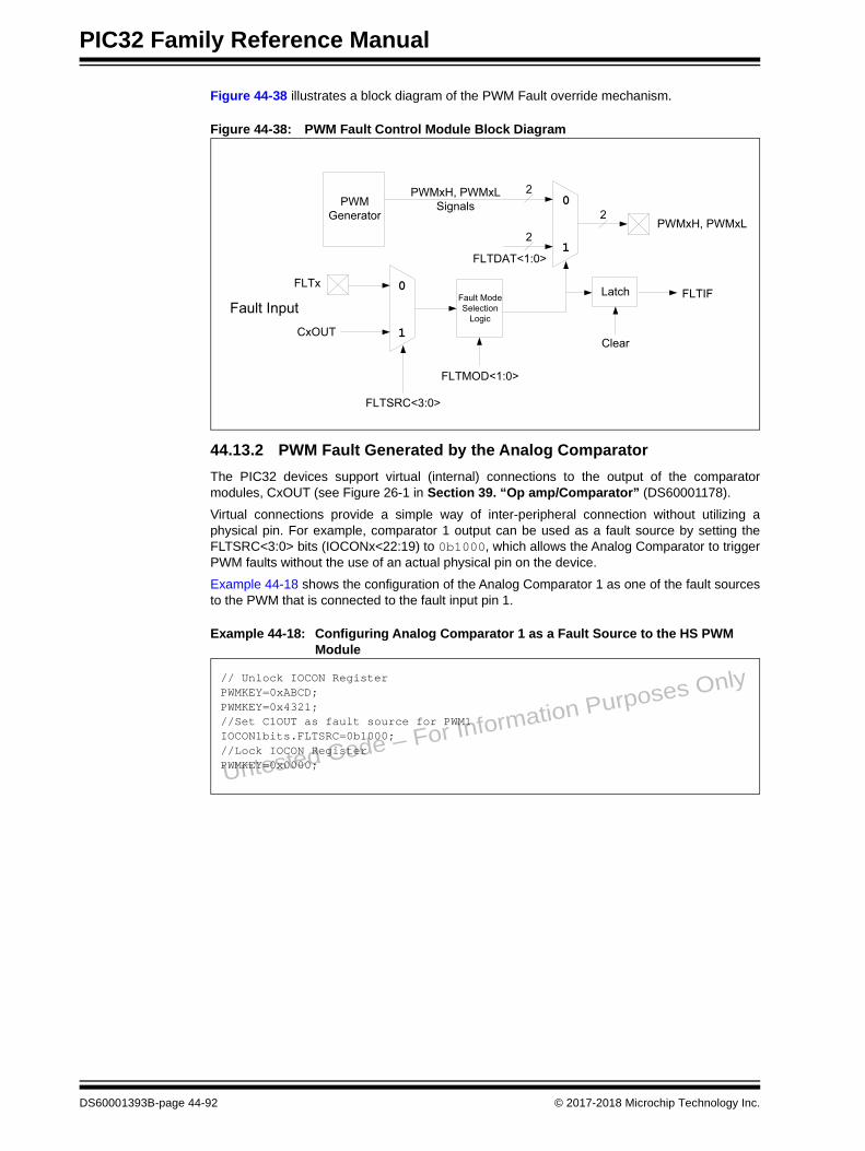
PIC32 Family Reference Manual
Figure 44-38 illustrates a block diagram of the PWM Fault override mechanism.
Figure 44-38: PWM Fault Control Module Block Diagram
44.13.2 PWM Fault Generated by the Analog Comparator
The PIC32 devices support virtual (internal) connections to the output of the comparatormodules, CxOUT (see Figure 26-1 in Section 39. “Op amp/Comparator” (DS60001178).
Virtual connections provide a simple way of inter-peripheral connection without utilizing aphysical pin. For example, comparator 1 output can be used as a fault source by setting theFLTSRC<3:0> bits (IOCONx<22:19) to 0b1000, which allows the Analog Comparator to triggerPWM faults without the use of an actual physical pin on the device.
Example 44-18 shows the configuration of the Analog Comparator 1 as one of the fault sourcesto the PWM that is connected to the fault input pin 1.
Example 44-18: Configuring Analog Comparator 1 as a Fault Source to the HS PWM Module
0
1
Fault Input0
1
FLTx
CxOUT
FLTSRC<3:0>
Fault Mode Selection
Logic
PWMGenerator
FLTMOD<1:0>
FLTDAT<1:0>
Latch FLTIF
PWMxH, PWMxL2
2
2
PWMxH, PWMxL Signals
Clear
Untested Code – For Information Purposes Only// Unlock IOCON RegisterPWMKEY=0xABCD;PWMKEY=0x4321;//Set C1OUT as fault source for PWM1IOCON1bits.FLTSRC=0b1000;//Lock IOCON RegisterPWMKEY=0x0000;
DS60001393B-page 44-92 © 2017-2018 Microchip Technology Inc.
Section 44. Motor Control PWM (MCPWM)
44.13.3 Fault Interrupts
The FLTIEN bit (PWMCONx<23>), determines whether an interrupt will be generated when theFLTx input is asserted high. The FLTDAT<1:0> bits (IOCONx<5:4>), supply the data values tobe assigned to the PWMxH and PWMxL pins in case of a fault.
The PWM Fault states are available on the FLTSTAT bit (PWMCONx<15>). The FLTSTAT bitdisplays the fault IRQ latch. If fault interrupts are not enabled, the FLTSTAT bit displays the statusof the selected FLTx input in positive logic format. When the fault input pins are not used inassociation with a PWM generator, these pins can be used as general purpose I/O or interruptinput pins.
44.13.3.1 FAULT INPUT MODES
The selected Fault and Current-Limit input signals are latched to capture the Current-Limit andFault input signals. The capture functions are asynchronous in recognizing Current-Limit or Faultsignal assertions. This insures that very short signal assertions or the advent of a clock systemfailure, a detected Fault or Current-Limit event can shutdown (i.e., deassert) the PWM outputs.
For intermittent Faults or Current-Limits, the latches are automatically cleared at the end of thePWM cycle if the Current-Limit and Fault signals have been deasserted.
The selected Fault input pin has two modes of operation that are selected using theFLTMOD<1:0> bits (IOCONx<17:16>):
• Latched mode: In Latched mode, the PWM outputs follow the states defined in the FLTDAT<1:0> bits, when the FLTx pin is asserted. The PWM outputs remain in this state until the fault pin is deasserted and the corresponding interrupt flag (FLTIF) has been cleared in software. When both of these actions have occurred, the PWM outputs return to normal operation at the beginning of the next PWM cycle boundary. If the FLTIF bit is cleared before the Fault condition ends, the outputs are held in their overridden states until the fault pin is no longer asserted. Since the FLTSTAT bit reflects the asserted state of the FLTx input pin it is persistent for as long as the fault exists.
• The user software therefore must poll for the FLTSTAT bit periodically when in the latched mode to determine a fault 'recovered' condition and then clear the FLTIF/CLIF flags to enable normal function.
• Cycle-by-Cycle mode: In Cycle-by-Cycle mode an event (Current-Limit and/or Fault) is held until the end of the current PWM cycle. At the start of the next PWM cycle, the state of the event is re-evaluated, which is based on the logic level assertion by external hardware on the chosen FLTx pin. If the Current-Limit or the Fault input is still asserted, the PWM outputs are held in the Fault or Current-Limit override states as given by the FLTDAT and CLDAT programmed, before the occurrence of the Fault condition. The purpose of this cycle-by-cycle re-evaluation is to provide the fastest and most reliable mechanism to transition out of the override state upon deassertion of the Fault and at the same time prevent the user software from polling for a Fault, which would cause PWM outputs to alternate between a Fault override state and operational states rapidly. This rapid transition of the PWM outputs can be detrimental to the application's output transistors.
The fault mode FLTMOD<1:0> bits can be protected from inadvertent writes by the PWMLOCKbit set to ‘0’ and the required write sequence.
Note 1: Changes take effect on the next PWM cycle boundary following PWM beingenabled, and subsequently on each PWM cycle boundary. When updating theFLTMOD<1:0> bits from ‘00’ or ‘01’ to ‘11’ (disabled), if the fault input is still activethe fault override condition will not be removed.
2: The Fault pins are also readable through the GPIO I/O logic when the PWM moduleis enabled. This allows the user to poll the state of the Fault pins in software.
© 2017-2018 Microchip Technology Inc. DS60001393B-page 44-93

PIC32 Family Reference Manual
Figure 44-39: Fault Timing Cycle Recovery Mode
Figure 44-40: Fault Timing Latched Mode
FLTDAT = b’10'PWMxH
FLTx
TMRx
FLTDAT = b’10'PWMxL
NORMAL FAULT OVERRIDE NORMAL NORMALFAULT OVERRIDE
Note: FLTPOL,CLPOL,POLH,POLL =’ 0',FLTDAT = ‘10’
P
FLTx
FLTIFx
TMRx
Software clears FLTIFx
FLTDAT = b’10'PWMxH
NORMAL NORMALFAULT OVERRIDE
P
DS60001393B-page 44-94 © 2017-2018 Microchip Technology Inc.

Section 44. Motor Control PWM (MCPWM)
44.13.4 Fault Entry
The Fault condition is asserted for the PWMxH and PWMxL pins according to the setting of theFLTDAT<1:0> bits. If the applicable bit is a logic ‘0’, an Asynchronous Reset of the pin occurs.Immediate shutdown occurs within 1 SYSCLK duration. If the applicable bit is a logic ‘1’, theassertion is delayed by the appropriate dead time (DTRx, ALTDTRx).
For more information on data sensitivity and behavior in response to current-limit or fault events,refer to 44.14.3 “Fault/Current-Limit Override and Dead Time Logic”.
44.13.5 Fault Exit
After a Fault condition has ended, the PWM signals must be restored at a PWM cycle boundaryto ensure proper synchronization of PWM signal edges and manual signal overrides. ForEdge-Aligned PWM mode, the next PWM cycle begins when the local time base (PTMRx) valueis zero. For Center-Aligned PWM mode, the next PWM cycle begins when the local time base(PTMRx) value is Period minus one.
If Cycle-by-Cycle Fault mode is selected, the fault is automatically reset on every PWM cycle. Noadditional software is needed to exit the Fault condition.
For Latched Fault mode, the following sequence must be followed to exit the Fault condition:
1. Poll the FLTSTAT or the associated GPIO pin for the FLTx pin to determine if the Faultsignal has been deasserted.
2. If the PWM Fault interrupt is not enabled, skip the following sub-steps and proceed to step 3. If the PWM Fault interrupt is enabled, perform the following sub-steps, and then proceed to step 4. a) Complete the PWM Fault Interrupt Service Routine (ISR).
b) Disable the PWM faults by setting the FLTMOD<1:0> = 11.c) Enable the latched PWM Fault mode by setting the FLTMOD<1:0>
bits (IOCONx<17:16>) = ‘0b00.
d) Clear the Fault Interrupt Flag by clearing the FLTIF bit (PWMCONx<31>).
e) Clear the PWM Interrupt Flag by clearing the corresponding IFS bit.
3. Disable PWM faults by setting the FLTMOD<1:0> = 11.
4. Enable the latched PWM Fault mode by setting the FLTMOD<1:0> bits = 00.
44.13.6 Fault Pin Software Control
The fault pin can be controlled manually in software. Since the fault input is shared with a GPIOport pin, this pin can be configured as an output by clearing the corresponding TRISx bit. Whenthe port bit for the GPIO pin is set, the fault input will be activated. The polarity or the active levelof the input is decided based on the selection made in FLTPOL.
Note: All digital inputs from the FLTx pins can be polled for or controlled in software asdescribed in this section. When the TRISx pin is set the status can be polled in soft-ware. When TRISx is cleared software can assert Fault, Current Limit or Dead Timecompensation.Care should be exercised when controlling the Fault inputs in the user software. Ifthe corresponding bit of the TRISx register for the Fault pin is cleared, the Faultinput cannot be driven externally.
© 2017-2018 Microchip Technology Inc. DS60001393B-page 44-95
PIC32 Family Reference Manual
44.14 PWM CURRENT-LIMIT
The key functions of the PWM current-limit pins are as follows:
• Each PWM generator can select its own current-limit input source with up to 16 Fault and current-limit pins and/or analog comparators. To configure the analog comparator as one of the current-limit sources, refer to 44.13.2 “PWM Fault Generated by the Analog Comparator”.
• Each PWM generator has control bits, Current-Limit Control Signal Source Select bits for PWM Generator ‘x’, CLSRC<3:0> (IOCONx<29:26>). These bits specify the source for its current-limit input signal.
• Each PWM generator has a corresponding Current-Limit Interrupt Enable bit, CLIEN (PWMCONx<22>). This bit enables the generation of current-limit IRQs.
• Each PWM generator has an associated Current-Limit Polarity bit for PWM Generator, CLPOL (IOCONx<25>). The current-limit pins are normally active-high. The CLPOL bit, if set to ‘1’, will invert the selected current limit input signal so that it is active-low.
• Upon occurrence of current-limit condition, the current limit override function, if enabled and active, forces the PWMxH/PWMxL pins to the values specified by the CLDAT<1:0> bits (IOCONx<3:2>)
The CLDAT<1:0> bits (IOCONx<3:2>) can have a value of either ‘0’ or ‘1’. If the CLDAT<1:0> bitis set to ‘00’, it is processed asynchronously to enable immediate shutdown of the associatedpower transistors in the application circuit. If CLDAT<1:0> is set to ‘11’, it is processed by thedead time logic and then applied to the PWM outputs.
The current-limit signals can generate interrupts. The CLIEN bit (PWMCONx<22>) controls thecurrent-limit interrupt signal generation. The user-assigned application can specify interruptgeneration even if the CLMOD bit (IOCONx<24>) disables the current-limit override function.This allows the current-limit input signal to be used as a general purpose external IRQ signal.
The current-limit input signal can be used as a trigger signal to the ADC, which initiates ananalog-to-digital conversion process. The ADC trigger signals are always active regardless of thestate of the MCPWM module, the CLMOD bit (IOCONx<24>), or the CLIEN bit(PWMCONx<22>). Refer to the “12 bit High-Speed Successive Approximation Register(SAR) Analog to Digital Converter (ADC)” chapter in the specific device data sheet for moreinformation on the ADC trigger sources.
A current-limit signal resets the time base for the affected PWM generator when the followingoccurs:
• The CLMOD bit for the PWM generator is ‘0’
• The External PWM Reset Control bit, XPRES (PWMCONx<1>), is ‘1’
• The PWM generator is in Independent Time Base mode (ITB bit (PWMCONx<9>) = 1)
This behavior is called Current Reset mode, which is used in some PFC applications.
Figure 44-41 illustrates the PWM current-limit control circuit logic.
DS60001393B-page 44-96 © 2017-2018 Microchip Technology Inc.

Section 44. Motor Control PWM (MCPWM)
Figure 44-41: PWM Current-Limit Control Module Block Diagram
44.14.1 Current-Limit Interrupts
The state of the PWM current-limit conditions is available on the CLSTAT bit (PWMCONx<14>).The CLSTAT bit displays the current-limit IRQ flag, if the CLIEN bit (PWMCONx<22>) is set. Ifcurrent-limit interrupts are not enabled, the CLSTAT bit displays the status of the selectedcurrent-limit inputs in positive logic format. When the current-limit input pin associated with aPWM generator is not used, these pins can be used as general purpose I/O or interrupt inputpins.
The current-limit pins are normally active-high. If set to ‘1’, the CLPOL bit (IOCONx<25>), invertsthe selected current-limit input signal and drives the signal into active-low state.
The interrupt generated by the selected current-limit input is combined with fault interrupt, triggerinterrupt, PWMH interrupt and PWML interrupt to create a single IRQ signal. This signal is sentto the interrupt controller, which has its own interrupt vector, interrupt flag bit, interrupt enable bit,and interrupt priority bits associated with it.
The fault pins are also readable through the port I/O logic when the MCPWM module is enabled.This capability allows the user-assigned application to poll the state of the fault pins in software.
44.14.2 Override Priority
When the PENH bit (IOCONx<15>) and the PENL bit (IOCONx<14>) are set, the followingpriorities apply to the PWM output:
• The Fault and Current-Limit are at the same priority level with override data on PWM pins.
• If only the Fault is active, the FLTDAT<1:0> bits (IOCONx<5:4>) override the manual override data and set the PWM outputs.
• If only the Current-Limit is active, the CLTDAT<1:0> bits (IOCONx<3:2>) override the man-ual override data and set the PWM outputs.
• If both the Fault and Current-Limit are simultaneously present, the override data with an inactive or deasserted state takes precedence. This means that only when both the override data (CLDAT and FLTDAT) for a particular pin are written with active or asserted data, the pin takes on an Asserted state after the applicable dead time delay. Otherwise, it asynchronously takes on the Deasserted state with no dead time delays.
• If neither a Fault nor a Current-Limit event is active, and a user Override Enable is set to the OVRENH bit and the OVRENL bit, the associated OVRDAT<1:0> bits (IOCONx<7:6>) set the PWM output.
• If no override conditions are active, the PWM signals generated by the time base and duty cycle comparator logic are the sources that set the PWM outputs.
© 2017-2018 Microchip Technology Inc. DS60001393B-page 44-97

PIC32 Family Reference Manual
Figure 44-42: Effect of Override Priority and Polarity on PWM Pins
Note: FLTPOL, CLPOL, POLH = 0, OVRENH = 0, OVRENL = 0.
(SeeNote)
(SeeNote)
DS60001393B-page 44-98 © 2017-2018 Microchip Technology Inc.

Section 44. Motor Control PWM (MCPWM)
44.14.3 Fault/Current-Limit Override and Dead Time Logic
In the event of a Fault and Current-Limit condition, the data in the FLTDAT<1:0> bits or theCLDAT<1:0> bits determine the state of the PWM I/O pins.
If any of the FLTDAT<1:0> bits or the CLDAT<1:0> bits contain inactive or deasserted logic level,the PWMxH and/or PWMxL outputs are driven inactive immediately, bypassing the dead timelogic. This behavior turns off the PWM outputs immediately without any additional delays. Thismay aid many power conversion/motor control applications that require a fast response to faultshutdown signals to limit circuitry damage and control system accuracy.
If any of the FLTDAT<1:0> bits or the CLDAT<1:0> bits contain active or asserted logic level, thePWMxH and/or PWMxL outputs are driven active immediately passing through the dead timelogic and, therefore, will be delayed by the specified dead time value. In this case, dead time willbe inserted even if a Fault or Current-Limit condition occurs.
44.14.4 Asserting Outputs through Current-Limit
In response to a Current-Limit event, the CLDAT<1:0> bits can be used to assert the PWMxHand PWMxL outputs. Such behavior could be used as a current force feature in response to anexternal current or voltage measurement that indicates a sudden sharp increase in the load onthe power-converter output. Forcing the PWM to an ‘ON’ state can be considered a feed-forwardaction that allows quick system response to unexpected load increases without waiting for thedigital control loop to respond.
Note: In Complementary PWM Output mode, the dead time generator remains activeunder all override conditions. The output overrides and fault overrides generatecontrol signals used by the dead time unit to set the outputs as requested, includingdead time.
© 2017-2018 Microchip Technology Inc. DS60001393B-page 44-99

PIC32 Family Reference Manual
44.15 SIMULTANEOUS PWM FAULTS AND CURRENT-LIMITS
If both current limit and fault events have been enabled, the PWMxH/PWMxL outputs will assertto deasserted/inactive if either the FLTDAT<1:0> bits (IOCONx<5:4>) or CLDAT<1:0>(IOCONx<3:2>) bits contain a deasserted state for a given PWM channel. The commandeddeasserted state is latched and it has priority over a current limit or fault override with an assertedstate.
Refer to 44.14.2 “Override Priority” for more information on the effects of simultaneousactivation of override inputs.
44.16 PWM FAULT AND CURRENT-LIMIT TRIGGER OUTPUTS TO ADC
The Fault and current-limit source selection bits, FLTSRC<3:0> (IOCONx<22:19>) andCLSRC<3:0> (IOCONx<29:26>), control multiplexers in each PWM generator module, whichselect the desired Fault and current-limit signals available to their respective modules. Theseselected Fault and current-limit signals are also provided to the ADC module for use as triggersignals that may be used to initiate ADC sampling and conversion operations.
These Fault and current-limit trigger signals to the ADC are always active regardless of the stateof the PTEN bit (PTCON<15>).
The multiplexer selection bits, CLSRC<3:0> and FLTSRC<3:0>, and the polarity control bits,CLPOL and FLTPOL (IOCONx<18>), are always actively controlling the selection and polarity ofthe signals to the ADC.
The Leading Edge Blanking (LEB) function is applied to these signals if the PTEN bit is ‘1’. If thePTEN bit is ‘0’, the LEB function is not applied to the current limit and fault ADC trigger signalsand the fault and current limit signals are directly connected to the ADC module.
The current-limit and Fault trigger signals to the ADC are also independent of the CLMOD bit(IOCONx<24>) and the FLTMOD<1:0> bits (IOCONx<17:16>).
Refer to “12 bit High-Speed Successive Approximation Register (SAR) Analog to DigitalConverter (ADC)” chapter in the specific device data sheet for more information on the ADCtrigger sources.
Example 44-19 provides the code for PWM Fault, current-limit and LEB configuration.
Example 44-19: PWM Fault, Current-Limit and Leading-Edge Blanking Configuration
Untested Code – For Information Purposes Only
/* PWM Fault, Current-Limit and Leading-Edge Blanking Configuration */
IOCON1bits.FLTMOD = 0; /* CLDAT<1:0> bits control PWMxH; FLTDAT<1:0> bits control PWMxL */IOCON1bits.CLSRC = 8; /* Current-limit input source is Analog Comparator 1 */IOCON1bits.FLTSRC = 9; /* Fault input source is Analog Comparator 2 */IOCON1bits.CLPOL = 1; /* Current-limit source is active-low */IOCON1bits.FLTPOL = 1; /* Fault Input source is active-low */IOCON1bits.CLMOD = 1; /* Enable current-limit function */IOCON1bits.FLTMOD = 1; /* Enable Cycle-by-Cycle Fault mode */IOCON1bits.FLTDAT = 0; /* PWMxH and PWMxL are driven inactive on occurrence of fault */IOCON1bits.CLDAT = 0; /* PWMxH and PWMxL are driven inactive on occurrence of current-limit */
LEBCON1bits.PHR = 1; /* Rising edge of PWMxH will trigger LEB counter */LEBCON1bits.PHF = 0; /* Falling edge of PWMxH is ignored by LEB counter */LEBCON1bits.PLR = 1; /* Rising edge of PWMxL will trigger LEB counter */LEBCON1bits.PLF = 0; /* Falling edge of PWMxL is ignored by LEB counter */LEBCON1bits.FLTLEBEN = 1; /* Enable fault LEB for selected source */LEBCON1bits.CLLEBEN = 1; /* Enable current-limit LEB for selected source */LEBDLY1bits.LEB = 8; /* Blank for a period (8 x Tosc) */
PWMCON1bits.XPRES = 0; /* External pins do not affect PWM time base reset */PWMCON1bits.FLTIEN = 1; /* Enable fault interrupt */PWMCON1bits.CLIEN = 1; /* Enable current-limit interrupt */
while (PWMCON1bits.FLTSTAT == 1); /* Wait when fault interrupt is pending */while (PWMCON1bits.CLSTAT == 1); /* Wait when current-limit interrupt is pending */
DS60001393B-page 44-100 © 2017-2018 Microchip Technology Inc.

Section 44. Motor Control PWM (MCPWM)
Figure 44-43: Current-Limit and Fault Trigger Mechanism
0000.
1111
0000.
1111
Note: Refer to the “12 bit High-Speed Successive Approximation Register (SAR) Analog to Digi-tal Converter (ADC)” chapter in the specific device data sheet for more information on the ADCtrigger sources.
© 2017-2018 Microchip Technology Inc. DS60001393B-page 44-101

PIC32 Family Reference Manual
44.17 SPECIAL FEATURES
The following special features are available in the MCPWM module:
• Leading-Edge Blanking (LEB)
• Chop mode
• Individual time base capture
• PWM pin swapping
• PWM output pin control and override
• Double update PWM mode
• Dead time compensation
44.17.1 Leading-Edge Blanking (LEB)
Each PWM generator supports LEB of the current-limit and fault inputs configured using the bitsin the Leading-Edge Blanking Control registers, LEBCONx and LEBDLYx. The purpose of LEBis to mask the transients that occur on the application printed circuit board when the powertransistors are turned ON and OFF.
The LEB bits are edge-sensitive. These bits support the blanking (ignoring) of the current-limitand fault inputs for a period of 0 to (4095 * TSYSCLK) following any specified rising or falling edgeof the PWMxH and PWMxL signals. Equation 44-11 provides the calculation for LEB.
Equation 44-11: Leading-Edge Blanking Calculation
In High-Speed Switching applications, switches (such as MOSFETs and IGBTs) typicallygenerate very large transients. These transients can cause measurement errors. The LEBfunction enables the user-assigned application to ignore the expected transients caused by theMOSFETs/IGBTs switching that occurs near the edges of the PWM output signals.
The PWMxH Rising Edge Trigger Enable bit (PHR) in the Leading-Edge Blanking Controlregister (LEBCONx<15), the PWMxH Falling Edge Trigger Enable bit, PHF (LEBCONx<14), thePWMxL Rising Edge Trigger Enable bit, PLR (LEBCONx<14), and the PWMxL Falling EdgeTrigger Enable bit, PLF (LEBCONx<12>), select the edge type of the PWMxH and PWMxLsignals, which starts the blanking timer. If a new selected edge triggers the LEB timer while thetimer is still active from a previously selected PWM edge, the timer reinitializes and continuescounting.
The Fault Input Leading-Edge Blanking Enable bit, FLTLEBEN (LEBCONx<11>), and theCurrent-Limit Leading-Edge Blanking Enable bit, CLLEBEN (LEBCONx<11>), enable theapplication of the blanking period to the selected fault and current-limit inputs.
Where,
LEBDLYx = Required leading edge blanking time
LEB Duration LEBDLYx<11:0> 1FSYSCLK--------------------------=
DS60001393B-page 44-102 © 2017-2018 Microchip Technology Inc.

Section 44. Motor Control PWM (MCPWM)
Figure 44-44 illustrates the masking of the Fault and Current-Limit signals from initiatingspurious override conditions. The different edges and associated configuration bits that can beused to re-trigger the delay counter are also shown.
Figure 44-44: Leading-Edge Blanking of Fault and Current-Limit Processing
Figure 44-45: Leading-Edge Blanking
Leading Edge
blanking Re-triggcounter
Current limits allowed
Faults allowed
PWMGenerator
‘x’
PWMxH
PWMxL
Rising and Falling edge
detection logic
PTCON.ON
PHR
PHF
PLR
PLF
FLTLEBEN
CLLEBEN(PTEN bit (PTCON<15>))
Switching Noise
Blanking time is determined by theLEB<9:3> bits in the LEBCONx registers
Fault and current-limitcircuitry ignores theswitching noise
PWM Output
High Power Signal
Blanking Signal
Power signal as seenby fault circuitry
© 2017-2018 Microchip Technology Inc. DS60001393B-page 44-103
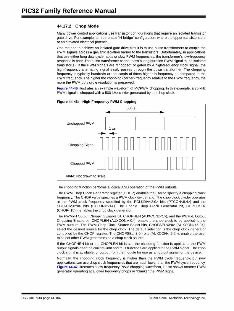
PIC32 Family Reference Manual
44.17.2 Chop Mode
Many power control applications use transistor configurations that require an isolated transistorgate drive. For example, a three-phase “H-bridge” configuration, where the upper transistors areat an elevated electrical potential.
One method to achieve an isolated gate drive circuit is to use pulse transformers to couple thePWM signals across a galvanic isolation barrier to the transistors. Unfortunately, in applicationsthat use either long duty cycle ratios or slow PWM frequencies, the transformer’s low-frequencyresponse is poor. The pulse transformer cannot pass a long duration PWM signal to the isolatedtransistor(s). If the PWM signals are “chopped” or gated by a high-frequency clock signal, thehigh-frequency alternating signal easily passes through the pulse transformer. The choppingfrequency is typically hundreds or thousands of times higher in frequency as compared to thePWM frequency. The higher the chopping (carrier) frequency relative to the PWM frequency, themore the PWM duty cycle resolution is preserved.
Figure 44-46 illustrates an example waveform of MCPWM chopping. In this example, a 20 kHzPWM signal is chopped with a 500 kHz carrier generated by the chop clock.
Figure 44-46: High-Frequency PWM Chopping
The chopping function performs a logical AND operation of the PWM outputs.
The PWM Chop Clock Generator register (CHOP) enables the user to specify a chopping clockfrequency. The CHOP value specifies a PWM clock divide ratio. The chop clock divider operatesat the PWM clock frequency specified by the PCLKDIV<2:0> bits (PTCON<6:4>) and theSCLKDIV<2:0> bits (STCON<6:4>). The Enable Chop Clock Generator bit, CHPCLKEN(CHOP<15>), enables the chop clock generator.
The PWMxH Output Chopping Enable bit, CHOPHEN (AUXCONx<1>), and the PWMxL OutputChopping Enable bit, CHOPLEN (AUXCONx<0>), enable the chop clock to be applied to thePWM outputs. The PWM Chop Clock Source Select bits, CHOPSEL<3:0> (AUXCONx<5:2>),select the desired source for the chop clock. The default selection is the chop clock generatorcontrolled by the CHOP register. The CHOPSEL<3:0> bits (AUXCONx<5:2>), enable the userto select other PWM generators as a chop clock source.
If the CHOPHEN bit or the CHOPLEN bit is set, the chopping function is applied to the PWMoutput signals after the current-limit and fault functions are applied to the PWM signal. The chopclock signal is available for output from the module for use as an output signal for the device.
Normally, the chopping clock frequency is higher than the PWM cycle frequency, but newapplications can use chop clock frequencies that are much lower than the PWM cycle frequency.Figure 44-47 illustrates a low-frequency PWM chopping waveform, it also shows another PWMgenerator operating at a lower frequency chops or “blanks” the PWM signal.
50 s
Unchopped PWM
Chopping Signal
Chopped PWM
1 s
Note: Not drawn to scale.
DS60001393B-page 44-104 © 2017-2018 Microchip Technology Inc.

Section 44. Motor Control PWM (MCPWM)
Figure 44-47: Low-Frequency PWM Chopping
44.17.3 Individual Time Base Capture
Each PWM generator has a Primary PWM Time Base Capture register (CAPx) that automaticallycaptures the independent time base counter value when the rising edge of the current-limit signalis detected. This feature is active only after the application of the LEB function. Theuser-assigned application should read the register before the next PWM cycle causes thecapture register to be updated again.
The Capture register is used in current mode control applications that use the analogcomparators or external circuitry to terminate the PWM duty cycle or period. By reading theindependent time base value at the current threshold, the user-assigned application cancalculate the slope of the current rise in the inductor. The secondary independent time base doesnot have an associated Capture register.
50 s
Chopping Signal
Unchopped PWM
Chopped PWM
Note: Not drawn to scale.
1 s
© 2017-2018 Microchip Technology Inc. DS60001393B-page 44-105

PIC32 Family Reference Manual
44.17.4 PWM Pin Swapping
The SWAP PWMxH and PWMxL Pins bit, SWAP (IOCONx<1>), if set to ‘1’, enables theuser-assigned application to connect the PWMxH signal to the PWMxL pin and the PWMxLsignal to the PWMxH pin. If the SWAP bit is set to ‘0’, the PWM signals are connected to theirrespective pins.
To perform the swapping function on the PWM cycle boundaries, the Output OverrideSynchronization bit, OSYNC (IOCONx<0>), must be set. If the user-assigned applicationchanges the state of the SWAP bit when the module is operating and the OSYNC bit is clear, theSWAP function will attempt to execute in the middle of a PWM cycle and the operation will yieldunpredictable results.
The SWAP function should be executed prior to the application of dead time. Dead timeprocessing is required since execution of switch function may enable the transistors in theuser-assigned application that are previously in disable state, possibly causing currentshoot-through.
The SWAP feature is useful for the applications that support multiple switching topologies with asingle application circuit board. It also enables the user-assigned application to change thetransistor modulation scheme in response to changing conditions.
The SWAP function can be implemented by using either of the following methods:
• Dynamic Swapping: In this method, the state of the SWAP bit can be changed dynamically based on the system response (for example, Switch Mode Power Supply (SMPS) Power Control)
• Static Swapping: In this method, the SWAP bit is set during the start-up configuration and remains unchanged during the program execution or on-the-fly (for example, Motor Con-trol)
44.17.4.1 EXAMPLE 1: PIN SWAPPING WITH SMPS POWER CONTROL
The SMPS Power Control example describes dynamic swapping. In power conversion/motorcontrol application, the transistor modulation technique can be changed between the full-bridgeZero Voltage Transition (ZVT) and standard full-bridge “on-the-fly” transition to meet differentload and efficiency requirements. As illustrated in Figure 44-48, the generic full-bridge convertercan operate in Push-Pull mode. The transistors are configured as follows:
• Q1 = Q4 • Q2 = Q3
The generic full-bridge converter can also operate in ZVT mode. The transistors are configuredas follows:
• Q1 = PWM1H• Q2 = PWM1L• Q3 = PWM2H• Q4 = P WM2L
Figure 44-48: SMPS Power Control
+
T1 VOUT
+VIN
Q1
Q2Q4
Q3
DS60001393B-page 44-106 © 2017-2018 Microchip Technology Inc.

Section 44. Motor Control PWM (MCPWM)
44.17.4.2 EXAMPLE 2: PIN SWAPPING WITH MOTOR CONTROL
The Motor Control example describes static swapping. Consider a generic motor control system,which is capable of driving two different types of motors, such as DC motors and three-phase ACinduction motors.
Brushed DC motors typically use a full-bridge transistor configuration, as illustrated inFigure 44-49. The Q1 and Q4 transistors are driven with similar waveforms, while the Q2 andQ3 transistors are driven with the complementary waveforms. This is also known as “driving thediagonals”. Note that the Q5 and Q6 transistors are not used in a brushed DC motor.
The transistors are configured as follows:
• Q1 = PWM1H
• Q2 = PWM1L
• Q3 = PWM2L
• Q4 = PWM2H
Figure 44-49: Motor Control
When compared to the DC motor, an AC induction motor uses all the transistors in the full-bridgeconfiguration. However, the significant difference is that the transistors are now driven as threehalf-bridges where the upper transistors are driven by the PWMxH outputs and the lowertransistors are driven by the PWMxL outputs.
The transistors are configured as follows:
• Q1 = PWM1H
• Q2 = PWM1L
• Q3 = PWM2H (note the difference with DC motors)
• Q4 = PWM2L (note the difference with DC motors)
• Q5 = PWM3H
• Q6 = PWM3L
Q1
Q2
Q3
Q4
Full-Bridge Converter
Q5
Q6
+VIN+VIN
© 2017-2018 Microchip Technology Inc. DS60001393B-page 44-107

PIC32 Family Reference Manual
44.17.5 PWM Output Pin Control and Override
If the MCPWM module is enabled, the priority of the PWMxH/PWMxL pin ownership from lowestto highest priority is as follows:
• PWM generator (lowest priority)• Swap function• PWM output override logic• Current-limit and Fault override logic
• GPIO/PWM ownership (highest priority)
If the MCPWM module is disabled, the GPIO module controls the PWMx pins.
Example 44-20 provides the code for PWM output pin assignment, Example 44-21 provides thecode for PWM output pins state selection, and Example 44-22 provides the code for enabling theMCPWM module.
Example 44-20: PWM Output Pin Assignment
Example 44-21: PWM Output Pins State Selection
Example 44-22: Enabling the Motor Control PWM (MCPWM) Module
44.17.5.1 PWM OUTPUT OVERRIDE LOGIC
The PWM output override feature is used to drive the individual PWM outputs to a desired statebased on system requirements. The output can be driven to both the active state as well as theinactive state.
The override feature has the following priority in descending order:
• Fault and Current-Limit overrides
• Manual override
All control bits associated with the PWM output override function are contained in the IOCONxregister. If the PWMxH Output Pin Ownership, PENH (IOCONx<15>), and the PWMxL OutputPin Ownership, PENL (IOCONx<14>) are set, the MCPWM module controls the PWMx outputpins. The PWM Output Override bits allow the user-assigned application to manually drive thePWM I/O pins to specified logic states, independent of the duty cycle comparison units.
The state of the PWMxH and PWMxL pins when manual override is in effect is determined by theoverride data bits, OVRDAT<1:0>(IOCONx<7:6>).
The manual override can be enforced individually on the PWMxH and PWMxL pins using theoverride enable bits OVERNH bit (IOCONx<9>) and the OVERNL bit (IOCONx<8), which areactive-high control bits.
All overrides, regardless of the cause, will be processed by the dead time control logic when it isenabled. This means active-low override data will be asynchronously reflected on the pins andthe active-high override data will be effective after the duration of the dead time depending onthe pin, as in normal dead time generation. Refer to section 44.8.3 “Dead Time Generation” fordetails.
Untested Code – For Information Purposes Only/* PWM Output pin control assigned to PWM generator */IOCON1bits.PENH = 1;IOCON1bits.PENL = 1;
Untested Code – For Information Purposes Only/* High and Low switches set to active-high state */IOCON1bits.POLH = 0;IOCON1bits.POLL = 0;
Untested Code – For Information Purposes Only/* Enable Motor Control PWM module */
PTCONbits.PTEN = 1;
DS60001393B-page 44-108 © 2017-2018 Microchip Technology Inc.

Section 44. Motor Control PWM (MCPWM)
Figure 44-50 illustrates priority of overrides when Faults and Current-Limit conditions occursimultaneously and their arbitration with respect to PWM polarities.
Figure 44-50: Fault and Current-Limit Override Priority on PWM Pins
44.17.5.2 PENX (GPIO/PWM) OWNERSHIP
Most of the PWM output pins are normally multiplexed with other GPIO pins. When the Debuggerhalts the device, the PWM pins will take the GPIO characteristics that is multiplexed on that pin.For example, if the PWM1L and PWM1H pins are multiplexed with RE0 and RE1, theconfiguration of GPIO pins will decide the PWM output status when halted by the Debugger.
Example 44-23 provides the code for GPIO configuration.
Example 44-23: GPIO Configuration Code Example
Manual Override
Current-LimitOverride
Fault Override
Dead Time Control and
PolarityCorrection
PWMxHPWMxL
2
2 2
2OVRENH OVRENL
OVRDAT
CLDAT
FLTDAT
FLTx
FLTy
Polarity corrected PWM high and
low
DTRx ALTDTRx
2 POLH POLL
0
1
0
1
0
1
Untested Code – For Information Purposes Only/* PWM output will be pulled to low when the device is halted by the
debugger */TRISE = 0x0000; RE0 and RE1 configured for an outputLATE = 0x0000; RE0 and RE1 configured as Low output
/* PWM output will be pulled to high when the device is halted by thedebugger */
TRISE = 0x0000; RE0 and RE1 configured for an outputLATE = 0x0003; RE0 and RE1 configured as High output
/* PWM output will be in tri-state when the device is halted by thedebugger */
TRISE = 0x0003; RE0 and RE1 configured for an input
© 2017-2018 Microchip Technology Inc. DS60001393B-page 44-109

PIC32 Family Reference Manual
44.17.6 Double Update Rate and Simultaneous Update Modes
Two cycle modes present two opportunities to update the duty cycles in a single PWM period.Each set of synchronized generators therefore can be updated with new duty cycles at periodmatch and counter rollover which effectively doubles the update rate compared to previousgeneration devices. Double update rate is available only with the Asymmetric center alignedmode.
At higher motor speeds, requirements inverters produce less than ideal waves due to finiteprocessing and Timer capabilities thereby causing harmonic distortion adding to the THD. Withdouble update rate lesser harmonic distortion is achieved because the waveform is closer to theideal. In normal dual cycle modes the resolution of the timer drops by factor of 2. Double updaterate regains the lost resolution.
Figure 44-51 shows the updates to PWM waveforms with updates to PDCx and SDCx done insoftware simultaneously. Refer to Figure 44-27 for double update rate mode.
Figure 44-51: Simultaneous Duty Cycle Update Mode in Asymmetric Center-Aligned Mode
The double update rate mode is configured by setting the ECAM<1:0> bits = 0b10. In this modeseparate writes to the PDCx and SDCx registers are required if rapid updates are desired. Theregisters, once written, will produce the intended waveform without the need to update everycycle. The PDCx register is written during the upwards count (PTDIR = 0) of the PTMRx andSDCx when the counter counts downwards (PTDIR = 1). This will ensure the update of the edgetransitions and therefore the duty cycle happen at the earliest possible instance.
DS60001393B-page 44-110 © 2017-2018 Microchip Technology Inc.

Section 44. Motor Control PWM (MCPWM)
The simultaneous update mode is configured by ECAM<1:0> bits = 0b11. In this mode writes tothe PDCx and SDCx registers take affect simultaneously at counter reload in the two cycleperiod. This mode is primarily used to regain the lost resolution in symmetric center alignedmodes with an extra write to the SDCx registers apart from the PDCx registers normally requiredfor Center-Aligned mode. Refer to Figure 44-16 for configuring the Channel/Generator in doubleupdate rate and simultaneous Asymmetric Center-Aligned modes.
44.17.6.1 ASYMMETRIC SYNCHRONOUS PWM MODE
For motor applications the traditional method of generating three phase sine waves forthree-phase star or delta connected wound motors was accomplished with a triangularmodulation scheme. Later modern methods added a zero sequence pattern to the waveforms.When strictly three terminal, (no current through the neutral in star connected motors) as inmotors, the zero sequence non-sinusoidal used to augment the modulation PWM provides anextra degree of freedom in waveform generation since the voltage between the neutral and DClink reference in VDC divided by 2 can have any waveform. A well designed zero sequencewaveform is added to alter the duty cycles on each of the three phases does not impact the lineto line voltage per PWM cycle on an average basis.
A carefully chosen zero sequence can achieve one or more of the following desirable properties.
• Reduced switching losses.
• Reduced total harmonic distortion
• Extended modulation depth/index
• Reduced Common mode drive voltage
The availability of asynchronous PWM mode with double and simultaneous update capabilityenables generation of synchronous multiphase waveforms that are discontinuous and symmetricor asymmetric with respect to each other.
When the augmenting zero sequence waveform is continuous, a continuous PWM scheme isproduced, as shown in Figure 44-52.
When the zero sequence is discontinuous with a high enough amplitude to cause the PWM toreach the positive or negative rails (VDC or 0), it results in discontinuous PWM, as shown inFigure 44-53. The discontinuous PWM scheme can significantly reduce switching losses for thesame power delivered when designed for reduced switching losses. This scheme is preferred inhigh ambient temperature applications.
Figure 44-54 shows discontinuous and asymmetric carrier modulation of the voltage waveformyielding Three-phase currents with reduced distortion. This method is preferred where switchinglosses reduction is important.
All of the previously described schemes can be employed at different times based on the ambienttemperature and load changes.
The double update rate is useful in applications where the modulation frequency is intentionallyreduced to keep switching losses low. When the fundamental frequency of the three-phase waveforms approach to within a tenth of the modulation frequency, the waveform integrity starts todepart from ideal due to the reduced relative output sampling rates. The double update helps torestore the waveform shape by effectively doubling the output sampling rate.
© 2017-2018 Microchip Technology Inc. DS60001393B-page 44-111

PIC32 Family Reference Manual
Figure 44-52: Symmetric Continuous Voltage Modulation with Conventional SVPWM
Figure 44-53: Symmetric Discontinuous Voltage Modulation
Phase
Phase
Phase
Phase Currents
Phase Voltages
Vo
Vo
Vo
0 10 20 30 40 50 60 70 80 90Time in Seconds
VDC
0
Volts
Time in Microseconds0 20 40 60 80 100 120 140 160 180
Phase A
Phase B
Phase C
Phase Currents
Phase Voltages
Voltage Phase A
Voltage Phase B
Voltage Phase C
VDC
0
Volts
Time in Microseconds
0 10 20 30 40 50 60 70 80 90Time in Seconds
0 20 40 60 80 100 120 140 160 180 200 220
DS60001393B-page 44-112 © 2017-2018 Microchip Technology Inc.

Section 44. Motor Control PWM (MCPWM)
Figure 44-54: Asymmetric and Discontinuous Voltage Modulation
Phase Currents
Phase Voltages
0 10 20 30 40 50 60 70 80 90Time in Seconds
VDC
Volts
Time in Microseconds
0
0 20 40 60 80 100 120 140 160 180
© 2017-2018 Microchip Technology Inc. DS60001393B-page 44-113

PIC32 Family Reference Manual
44.17.7 Dead Time Compensation
Dead time compensation is used mostly in three-phase PWM-based inverters for motor control.
The purpose of compensation is largely to reduce harmonic distortion in the phase currents. Asignificant contributor to the distortion is “conduction dead times” that reduce or increase thesoftware intended voltseconds of the phase voltage waveforms, which in turn affect the currentconduction time of the high-side and low-side power devices.
The dead times (DTRx, ALTDTRx) become a more prominent contributor to the voltsecondsdistortion of the phase voltage waveforms at low speeds and low torques (i.e., low duty cycles).
Dead time can be compensated for with the knowledge of the current direction in the phases.The currents are usually compared in run-time for zero-crossings using comparators, and adigital input, DTCMPx, is used to automatically compensate for the excess and reduction in dutycycles in hardware. Digital comparators that are available on dedicated analog inputs can beused to monitor for current magnitudes/direction change to achieve better dead timecompensation.
Figure 44-55 shows the desired ideal line to line voltage and current waveforms and theircorresponding actual or non-ideal waveforms with conventional space vector modulation for asingle phase. The distortion is exaggerated for clarity. A fully compensated inverter achievesnear-ideal current waveforms with very little harmonic distortion.
Figure 44-55: Ideal/Compensated Waveforms Versus Uncompensated Waveforms
Desired VoltageDesired CurrentActual VoltageActual Current
DS60001393B-page 44-114 © 2017-2018 Microchip Technology Inc.

Section 44. Motor Control PWM (MCPWM)
Figure 44-56 shows an under-compensated line to line voltage and current waveform when dutycycle is reduced below dead time or exceeded above “period-dead time” values. In addition, thefigure shows the effect of dead time on current harmonic distortion and correction usingcompensation by adjustments to dead time values.The voltage and as a consequence thecurrent waveform shows significant distortion and this distortion is accentuated at lowerfrequencies. The extent of distortion is even more aggravated when the amplitude gets smaller(lower duty cycles). See 44.8.5 “Dead Time Distortion” for details. To support full compensationat all duty cycles, the MCPWM module is capable of runtime updates to the dead time registers.The DTCOMPx value compensates only to the extent of the actual dead time generated (valuein DTRx/ALTDTRx) so merely writing higher values to the DTCOMPx register under the aboveconditions will be in-effective and can cause waveform distortion.
Figure 44-56: Harmonic Distortion and Mitigation at Duty Cycle Extremes
When the dead time registers are updated on-the-fly, as shown in Equation 44-12, the harmonicdistortion can be further reduced.
Desired VoltageDesired CurrentActual VoltageActual Current
© 2017-2018 Microchip Technology Inc. DS60001393B-page 44-115

PIC32 Family Reference Manual
Equation 44-12: Dead Time Adjustments for Reduction of Harmonic Distortion
When the duty cycle exceeds the range bounded by Period minus the sum of dead times,distortion of wave form ensues. This occur because the duty cycle saturates and updates haveno effect. Rectifying this situation requires more than writing to the DTCOMPx registers. Thedead time registers need to be reduced for that period, and therefore, runtime writes to DTRx andALTDTRx are required. When dead time values are reduced, it is done symmetrically bysubtracting from both the dead time registers together. This is a strategy that will have to be doneevery cycle whether or not the PWM duty cycle exceeds the boundary. When it does not exceedthe boundary, the actual dead time values imposed by hardware are used.
When it exceeds the of normal range boundary, one of the PWM lines is at 0% duty cycle, andtherefore, there is no need for dead time generation. Consequently, writing lesser values to thedead time registers (DTRx and ALTDTRx) will not have a shoot through effect in the powerstages.
DTRx HWLDT Period MaxDuty– 2-----------------------------------------------------–=
ALTDTRx HWTDT Period MaxDuty– 2-----------------------------------------------------–=
When the desired Duty Cycle exceeds maximum duty (MaxDuty):
DTRx HWLDT MinDuty Period– 2----------------------------------------------------–=
ALTDTRx HWTDT MinDuty Period– 2----------------------------------------------------–=
When the desired Duty Cycle is less than minimum duty (MinDuty):
Where:
Period = STPER/PTPER/PHASEx
MaxDuty = Period – ALTDTRx – DTRxMinDuty = ALTDTRx + DTRx
HWLDT = Leading-edge dead time counts required by hardwareHWTDT = Trailing-edge dead time counts required by hardware
ALTDTRx HWTDT=
When the desired Duty Cycle is within minimum duty and maximum duty (MinDuty and MaxDuty):
DTRx HWLDT=
DS60001393B-page 44-116 © 2017-2018 Microchip Technology Inc.

Section 44. Motor Control PWM (MCPWM)
44.18 POWER-SAVING MODES
This section discusses the operation of the MCPWM module in Sleep mode and Idle mode.
44.18.1 Motor Control PWM (MCPWM) Operation in Sleep Mode
When the device enters Sleep mode, the system clock is disabled. Since the clock for the PWMtime base is derived from the system clock source (TSYSCLK), that clock will also be disabledand all enabled PWM output pins that were in effect prior to entering Sleep mode will be frozenin the output states. If the MCPWM module is used to control a load in a power application, theMCPWM module outputs must be placed into a safe state before putting the device in Sleepmode. Depending on the application, the load may begin to consume excessive current when thePWM outputs are frozen in a particular output state. In such a case, the override functionality canbe used to drive the PWM output pins into the inactive state.
If the fault inputs are configured for the MCPWM module, the fault input pins continue to functionnormally when the device is in Sleep mode. If the fault pin associated with the PWM generatorby FLTSRC<3:0> bits is asserted active, the PWM outputs are driven to preprogrammed Faultstates held in FLTDAT<1:0>. The fault input pins can also wake the CPU from Sleep mode. If thefault pin interrupt priority is greater than the current CPU priority, program execution starts at thefault pin interrupt vector location upon wake-up. Otherwise, execution continues from the nextinstruction following the PWRSAV instruction.
44.18.2 MCPWM Operation in Idle Mode
The PWM module consists of a PWM Time Base Stop in Idle Mode Control bit,PTSIDL (PTCON<13>). The PTSIDL bit (PTCON<13>) determines if the PWM module willcontinue to operate or stop when the device enters Idle mode. If PTSIDL = 0, the module willcontinue to operate as normal. If PTSIDL = 1, the module will shut down and stop its internalclocks. The system will not be able to access the SFRs in this mode. This will be the minimumpower mode for the module. Stopped Idle mode functions, such as Sleep mode and fault pins willbe asynchronously active. The control of the PWM pins will revert back to the GPIO bitsassociated with the PWM pins if the PWM module enters an Idle state.
It is recommended that the user-assigned applications disable the PWM outputs prior to enteringIdle mode. If the PWM module is controlling a power conversion/motor control application, theaction of putting the device into Idle mode will cause any control loops to be disabled, and mostapplications will likely experience issues unless they are explicitly designed to operate in an openloop mode.
Note: Refer to Section 10. “Power-Saving Modes” (DS60001130), for more information.
© 2017-2018 Microchip Technology Inc. DS60001393B-page 44-117

PIC32 Family Reference Manual
44.19 EXTERNAL CONTROL OF INDIVIDUAL TIME BASE(S)
External signals can reset the primary dedicated time bases, if the XPRES bit (PWMCONx<1>)is set. This mode of operation is called Current Reset PWM mode. If the user-assignedapplication sets the ITB bit (PWMCONx<9>), a PWM generator operates in Independent TimeBase mode. If the user-assigned application sets the XPRES bit and operates the PWMgenerator in Master Time Base mode, the results may be unpredictable.
The current-limit source signal specified by the CLSRC<3:0> bits (IOCONx<29:26>) causes theindependent time base to reset. The active edge of the selected current-limit signal is specifiedby the CLPOL bit (IOCONx<25>).
In Independent Time Base mode, some PFC applications need to maintain the inductor currentvalue above minimum desired current level. These applications use the external Reset feature.If the inductor current falls below the desired value, the PWM cycle is terminated early so thatthe PWM output can be asserted to increase the inductor current. The PWM period variesaccording to the application needs. This type of application is a variable frequency PWM mode.
44.20 APPLICATION INFORMATION
Typical applications that use different PWM operating modes and features are as follows:
• Complementary Output Mode
• Push-Pull Output Mode
• Multi-Phase PWM
• Variable Phase PWM
• Current Reset PWM
• Constant Off-Time PWM
• Current-Limit PWM
Each application is described in the following sections.
DS60001393B-page 44-118 © 2017-2018 Microchip Technology Inc.

Section 44. Motor Control PWM (MCPWM)
44.20.1 Complementary Output Mode
The Complementary PWM mode, illustrated in Figure 44-57, is generated in a manner that issimilar to Standard Edge-Aligned mode. This mode provides a second PWM output signal on thePWMxL pin that is the complement of the primary PWM signal (PWMxH). Figure 44-58illustrates the complementary PWM output mode for motor control.
Figure 44-57: Complementary PWM Output Mode for SMPS
Figure 44-58: Complementary PWM Output Mode for Motor Control
Synchronous Buck ConverterSeries Resonant/LLC Half-Bridge Converter
PWM1L
PWM1H
Dead Time(1) Dead Time(1) Dead Time(1)
Period
Period
Duty Cycle
0
Period
TimerValue
Timer Resets
PWMxH
Value
PWMxL (Period-duty cycle)
Duty Cycle Match
Note 1: Positive Dead Time shown.
VOUTL1
+VIN
PWM1H
PWM1L
+
+
+VIN
PWM1H
PWM1L
CR T1LR VOUT
PWM1H
PWM1L
PWM2H
PWM2L
PWM3H
PWM3L
3-Phase Motor
© 2017-2018 Microchip Technology Inc. DS60001393B-page 44-119

PIC32 Family Reference Manual
44.20.2 Push-Pull Output Mode
Push-Pull PWM Output mode, illustrated in Figure 44-59, alternately outputs the PWM signal onone of two PWM pins. In this mode, complementary PWM output is not available. This mode isuseful in transformer-based power converter circuits that avoid flow of direct current thatsaturates their cores. Push-Pull mode ensures that the duty cycle of the two phases is identical,thereby yielding a net DC bias of zero.
Figure 44-59: Push-Pull PWM Output Mode
T1
++VIN
PWM1H
PWM1L
Push-Pull Buck Converter
L1 VOUT
PWM1H
PWM1L
DCX - DTR
Period - DCX + DTR
TON
TOFF
Period Period
Dead Time Dead Time Dead Time
Period
Duty Cycle
0
Period
TimerValue
Timer Resets
PWMxH
Value
PWMxL Duty Cycle
Duty Cycle Match
Half-Bridge Converter+VIN
+
T1VOUT
PWM1H
PWM1L
+
L1
+
PWH1H PWH1L
PWH1H
+VIN
T1
L1 VOUT
Full-Bridge Converter
+
PWH1L
DS60001393B-page 44-120 © 2017-2018 Microchip Technology Inc.

Section 44. Motor Control PWM (MCPWM)
44.20.3 Multi-Phase PWM
The Multi-Phase PWM, illustrated in Figure 44-60, uses phase shift values in the PHASExregisters to shift the PWM outputs with respect to the primary time base. Because the phase shiftvalues are added to the primary time base, the phase shifted outputs occur earlier than a PWMsignal that specifies zero phase shifts. In Multi-Phase mode, the specified phase shift is fixed bythe application’s design. Phase shift is available in all PWM modes that use the master time base.
Multi-phase PWM is often used in DC-to-DC converters that handle fast load current transients,and need to meet smaller space requirements. A multi-phase converter is essentially a parallelarray of buck converters that are operated slightly out of phase with each other. The multiplephases create an effective switching speed equal to the sum of the individual converters.
If a single phase is operating at a PWM frequency of 333 kHz, the effective switching frequencyfor the circuit, shown in Figure 44-61, is 1 MHz. This high switching frequency reduces input andoutput capacitor size requirements. It also improves load transient response and ripple figures.
Figure 44-60: Multi-Phase PWM
+
PWM2H PWM3H
L1L2
L3
PWM1L PWM2L PWM3L
VOUT
Multi-Phase DC/DC Converter
PWM1H
PWM1L
PWM2H
PWM2L
PWM3H
PWM3L
+VIN
PWM1H
© 2017-2018 Microchip Technology Inc. DS60001393B-page 44-121

PIC32 Family Reference Manual
44.20.3.1 INTERLEAVED POWER FACTOR CORRECTION (IPFC)
The interleaving of multiple boost converters in PFC circuits is becoming popular in the recentapplications. Figure 44-61 and Figure 44-62 illustrate the typical IPFC circuit configuration andthe IPFC operational waveforms.
Figure 44-61: Interleaved PFC Diagram
Figure 44-62: Interleaved PFC Operational Waveforms
By staggering the channels at uniform intervals, multichannel IPFC can reduce the input currentripple significantly due to the ripple cancellation effect. The smaller input current ripple indicatesthe low Differential Mode (DM) noise filter. It is generally believed that the reduced Differentialmode noise magnitude makes Differential mode filter smaller. The output capacitor voltageripples are also reduced significantly as a function of the duty cycle.
PWM1
PWM2
PF
C O
utp
ut
IIN9
0V
- 2
65
VR
ect
ifie
r
IL1 ID1 ILoad
Ic
IS1
IL2ID2
IS2
When duty cycle is = 50%When duty cycle is > 50%
PWM1
PWM2
IL1
IL2
(IL1 + IL2)
PWM1
PWM2
IL1
IL2
(IL1 + IL2)
DS60001393B-page 44-122 © 2017-2018 Microchip Technology Inc.
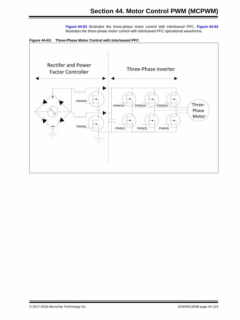
Section 44. Motor Control PWM (MCPWM)
Figure 44-63 illustrates the three-phase motor control with interleaved PFC. Figure 44-64illustrates the three-phase motor control with interleaved PFC operational waveforms.
Figure 44-63: Three-Phase Motor Control with Interleaved PFC
ThreePhaseMotor
+PWM4H
PWM4L PWM1L PWM2L PWM3L
PWM1H PWM2H PWM3H
Rectifer and PowerFactor Controller Three Phase inverter
© 2017-2018 Microchip Technology Inc. DS60001393B-page 44-123

PIC32 Family Reference Manual
Figure 44-64: Three-Phase Motor Control with Interleaved PFC Operational Waveforms
Three-Phase Inverter Synchronized PWM Cycle
PWM1H
PWM1L
PWM2L
PWM3L
PWM2H
PWM3H
PWM4L
PFC Controller Push-Pull PWM Cycle
PHASE4
PWM4H
PWM4L
PDC4
PWM4H
DS60001393B-page 44-124 © 2017-2018 Microchip Technology Inc.

Section 44. Motor Control PWM (MCPWM)
44.20.4 Variable Phase PWM
The Variable Phase PWM, illustrated in Figure 44-65, constantly changes the phase shift amongPWM channels to control the flow of power, which is in contrast with most PWM circuits that varythe duty cycle of PWM signal to control power flow. In variable phase applications, the PWM dutycycle is often maintained at 50%. The phase shift value is available to all PWM modes that usethe master time base.
The variable phase PWM is used in newer power conversion/motor control topologies that aredesigned to reduce switching losses. In the standard PWM methods, when a transistor switchesbetween the conducting state and the non-conducting state (and vice versa), the transistor isexposed to full current and voltage condition during the time when the transistor turns ON or OFFand the power loss (V * I * TSW * FPWM) becomes appreciable at high frequencies.
The Zero Voltage Switching (ZVS) and Zero Current Switching (ZVC) circuit topologies attemptto use quasi-resonant techniques that shift either the voltage or the current waveforms relativeto each other to change the value of voltage or the current to zero when the transistor turns ONor OFF. If either the current or the voltage is zero, no switching loss occurs.
Figure 44-65: Variable Phase PWM
PWM1H
PWM1L
PWM2HPWM2L
Variable Phase Shift
Duty CyclePWM1H
Period
Duty Cycle
Duty Cycle
Phase 2 (old value)
Duty Cycle
PWM2H
Phase 2 (new value)
+
Full-Bridge ZVT Converter
T1VOUT
+VIN
PWM1H
PWM1L PWM2L
PWM2H
© 2017-2018 Microchip Technology Inc. DS60001393B-page 44-125

PIC32 Family Reference Manual
44.20.5 Current Reset PWM
The Current Reset PWM, illustrated in Figure 44-66, is a variable frequency mode, where theactual PWM period is less than or equal to the specified period value. The independent time baseis reset externally after the PWM signal has been deasserted. The Current Reset PWM modecan be used in Constant PWM On-Time mode. To operate in PWM Current Reset, the PWMgenerator should be in Independent Time Base. If an external Reset signal is not received, bydefault, the PWM period uses the PHASEx register value.
In Current Reset mode, the PWM frequency varies with the load current. This is different frommost PWM modes because the user-assigned application sets the maximum PWM period andan external circuit measures the inductor current. When the inductor current falls below aspecified value, the external current comparator circuit generates a signal that resets the PWMtime base counter. The user-assigned application specifies a PWM ‘ON’ time, and then sometime after the PWM signal becomes inactive, the inductor current falls below a specified valueand the PWM counter is reset earlier than the programmed PWM period. This is called ConstantOn-Time Variable Frequency PWM output and is used in Critical Conduction mode PFCapplications.
This should not be confused with the cycle-by-cycle current-limiting PWM output, where thePWM output is asserted, an external circuit generates a current fault, and the PWM signal isturned off before its programmed duty cycle will normally turn it off. Here, the PWM frequency isfixed for a given time base period.
The advantages of Current Reset PWM mode in PFC applications are as follows:
• As the PFC boost inductor does not require to store energy at the end of each switching cycle, a smaller inductor can be used. The usage of the smaller inductor leads to reduced cost.
• Commutation of Boost diode from ON to OFF happens at zero current. The slower diodes can be used to reduce the cost.
• Inner current feedback loop is much faster, as the feedback is received for every cycle
Note: In Current Reset mode, the local time base resetting is based on the blanked activelevel of the current-limit input signal after completion of the PWMxH/PWMxL dutycycle.
DS60001393B-page 44-126 © 2017-2018 Microchip Technology Inc.

Section 44. Motor Control PWM (MCPWM)
Figure 44-66: Current Reset PWM
External current comparator resets PWM counter. PWM cycle restarts earlier than the programmed period. This is a Constant On-time Variable Frequency PWM mode.
Fa
ult
So
urc
e
Targeted Voltage
PID
ADC
Virtual I/O
Control
+ACIN
LIL
PWMxH/
D VOUT
COUT
˜
Motor ControlPWM Generator CVREF
Comp
PWMxL
© 2017-2018 Microchip Technology Inc. DS60001393B-page 44-127

PIC32 Family Reference Manual
44.20.6 Constant Off-Time PWM
Constant Off-Time PWM, illustrated in Figure 44-67, is a variable-frequency PWM output wherethe actual PWM period is less than or equal to the specified period value. The PWM time baseresets externally after the PWM signal duty cycle value has been reached and the PWM signalhas been deasserted. This is implemented by enabling the On-Time PWM output called CurrentReset PWM and using the complementary PWM output (PWMxL).
The Constant Off-Time PWM can be enabled only when the PWM generator operates inindependent time base. If an external Reset signal is not received, by default, the PWM perioduses the value specified in the PHASEx register.
Figure 44-67: Constant Off-Time PWM
Duty Cycle
0
Period
TimerValue
Programmed Period
PWMxL
Value
External Timer Reset
Duty Cycle
Actual Period
External Timer Reset
Note: Duty Cycle represents OFF time.
DS60001393B-page 44-128 © 2017-2018 Microchip Technology Inc.

Section 44. Motor Control PWM (MCPWM)
44.20.7 Current-Limit PWM
The cycle-by-cycle current-limit, illustrated in Figure 44-68, cut short the asserted PWM signalwhen the selected external fault signal is asserted. The PWM output values are specified by theCLDAT<1:0> bits (IOCONx<3:2>). The override outputs remain in effect until the beginning ofthe next PWM cycle. This is sometimes used in the PFC circuits, where the inductor currentcontrols the PWM On-Time. This is a constant frequency PWM.
Figure 44-68: Current-Limit PWM
44.20.8 Discontinuous or Burst Mode Implementation
In applications where the load current drawn from the converter is smaller than its nominalcurrent/converter operating at no load, the power drawn from the source can be reduced byforcing the converter to deassert the PWM output by using manual override. Typically, theconverter PWM output can be turned off over a period of time based on the output voltageregulation, which can reduce the no load power requirements significantly.
+
L
IL
PWMxH/PWMxL
DVOUT
COUT
˜S
PWMxH/
PWMxH/ New Duty Cycle
IL
Programmed Duty Cycle
Current-Limit
Duty Cycle
0
Period
PWMxH/
Value
FLTx Negates PWM
Duty CycleProgrammed
Duty Cycle
Programmed
Duty Cycle
PWMxH/
Duty CycleActual Actual
FLTx Negates PWM
Programmed Period
Current-Limit
PWMxL
PWMxL
PWMXL
PWMxL
© 2017-2018 Microchip Technology Inc. DS60001393B-page 44-129

PIC32 Family Reference Manual
44.21 RELATED APPLICATION NOTES
This section lists application notes that are related to this section of the manual. Theseapplication notes may not be written specifically for the PIC32 device family, but the concepts arepertinent and could be used with modification and possible limitations. The current applicationnotes related to the Motor Control PWM (MCPWM) module are:
Title Application Note #
No related application notes are available at this time. N/A
Note: Please visit the Microchip web site (www.microchip.com) for additional ApplicationNotes and code examples for the PIC32 family of devices.
DS60001393B-page 44-130 © 2017-2018 Microchip Technology Inc.

Section 44. Motor Control PWM (MCPWM)
44.22 REVISION HISTORY
Revision A (May 2017)
This is the initial released version of the document.
Revision B (October 2018)
• Added a footnote for the Trigger Compare Register value in order to Generate a trigger at period boundary
• Footnote added to the TRGCONx register to caution about double trigger generation in dual cycle PWM modes
• Made timing diagram corrections for Figure 44-31, Figure 44-36, and Figure 44-37
• Made labeling corrections for Figure 44-32, Figure 44-33, Figure 44-34, Figure 44-35, Figure 44-36, and Figure 44-37
© 2017-2018 Microchip Technology Inc. DS60001393B-page 44-131

PIC32 Family Reference Manual
NOTES:
DS60001393B-page 44-132 © 2017-2018 Microchip Technology Inc.
Note the following details of the code protection feature on Microchip devices:
• Microchip products meet the specification contained in their particular Microchip Data Sheet.
• Microchip believes that its family of products is one of the most secure families of its kind on the market today, when used in the intended manner and under normal conditions.
• There are dishonest and possibly illegal methods used to breach the code protection feature. All of these methods, to our knowledge, require using the Microchip products in a manner outside the operating specifications contained in Microchip’s Data Sheets. Most likely, the person doing so is engaged in theft of intellectual property.
• Microchip is willing to work with the customer who is concerned about the integrity of their code.
• Neither Microchip nor any other semiconductor manufacturer can guarantee the security of their code. Code protection does not mean that we are guaranteeing the product as “unbreakable.”
Code protection is constantly evolving. We at Microchip are committed to continuously improving the code protection features of ourproducts. Attempts to break Microchip’s code protection feature may be a violation of the Digital Millennium Copyright Act. If such actsallow unauthorized access to your software or other copyrighted work, you may have a right to sue for relief under that Act.
Information contained in this publication regarding deviceapplications and the like is provided only for your convenienceand may be superseded by updates. It is your responsibility toensure that your application meets with your specifications.MICROCHIP MAKES NO REPRESENTATIONS ORWARRANTIES OF ANY KIND WHETHER EXPRESS ORIMPLIED, WRITTEN OR ORAL, STATUTORY OROTHERWISE, RELATED TO THE INFORMATION,INCLUDING BUT NOT LIMITED TO ITS CONDITION,QUALITY, PERFORMANCE, MERCHANTABILITY ORFITNESS FOR PURPOSE. Microchip disclaims all liabilityarising from this information and its use. Use of Microchipdevices in life support and/or safety applications is entirely atthe buyer’s risk, and the buyer agrees to defend, indemnify andhold harmless Microchip from any and all damages, claims,suits, or expenses resulting from such use. No licenses areconveyed, implicitly or otherwise, under any Microchipintellectual property rights unless otherwise stated.
2017-2018 Microchip Technology Inc.
Microchip received ISO/TS-16949:2009 certification for its worldwide headquarters, design and wafer fabrication facilities in Chandler and Tempe, Arizona; Gresham, Oregon and design centers in California and India. The Company’s quality system processes and procedures are for its PIC® MCUs and dsPIC® DSCs, KEELOQ® code hopping devices, Serial EEPROMs, microperipherals, nonvolatile memory and analog products. In addition, Microchip’s quality system for the design and manufacture of development systems is ISO 9001:2000 certified.
QUALITY MANAGEMENT SYSTEM CERTIFIED BY DNV
== ISO/TS 16949 ==
Trademarks
The Microchip name and logo, the Microchip logo, AnyRate, AVR, AVR logo, AVR Freaks, BitCloud, chipKIT, chipKIT logo, CryptoMemory, CryptoRF, dsPIC, FlashFlex, flexPWR, Heldo, JukeBlox, KeeLoq, Kleer, LANCheck, LINK MD, maXStylus, maXTouch, MediaLB, megaAVR, MOST, MOST logo, MPLAB, OptoLyzer, PIC, picoPower, PICSTART, PIC32 logo, Prochip Designer, QTouch, SAM-BA, SpyNIC, SST, SST Logo, SuperFlash, tinyAVR, UNI/O, and XMEGA are registered trademarks of Microchip Technology Incorporated in the U.S.A. and other countries.
ClockWorks, The Embedded Control Solutions Company, EtherSynch, Hyper Speed Control, HyperLight Load, IntelliMOS, mTouch, Precision Edge, and Quiet-Wire are registered trademarks of Microchip Technology Incorporated in the U.S.A.
Adjacent Key Suppression, AKS, Analog-for-the-Digital Age, Any Capacitor, AnyIn, AnyOut, BodyCom, CodeGuard, CryptoAuthentication, CryptoAutomotive, CryptoCompanion, CryptoController, dsPICDEM, dsPICDEM.net, Dynamic Average Matching, DAM, ECAN, EtherGREEN, In-Circuit Serial Programming, ICSP, INICnet, Inter-Chip Connectivity, JitterBlocker, KleerNet, KleerNet logo, memBrain, Mindi, MiWi, motorBench, MPASM, MPF, MPLAB Certified logo, MPLIB, MPLINK, MultiTRAK, NetDetach, Omniscient Code Generation, PICDEM, PICDEM.net, PICkit, PICtail, PowerSmart, PureSilicon, QMatrix, REAL ICE, Ripple Blocker, SAM-ICE, Serial Quad I/O, SMART-I.S., SQI, SuperSwitcher, SuperSwitcher II, Total Endurance, TSHARC, USBCheck, VariSense, ViewSpan, WiperLock, Wireless DNA, and ZENA are trademarks of Microchip Technology Incorporated in the U.S.A. and other countries.
SQTP is a service mark of Microchip Technology Incorporated in the U.S.A.
Silicon Storage Technology is a registered trademark of Microchip Technology Inc. in other countries.
GestIC is a registered trademark of Microchip Technology Germany II GmbH & Co. KG, a subsidiary of Microchip Technology Inc., in other countries.
All other trademarks mentioned herein are property of their respective companies.
© 2018, Microchip Technology Incorporated, All Rights Reserved.
ISBN: 978-1-5224-3756-7
DS60001393B-page 133

DS60001393B-page 134 2017-2018 Microchip Technology Inc.
AMERICASCorporate Office2355 West Chandler Blvd.Chandler, AZ 85224-6199Tel: 480-792-7200 Fax: 480-792-7277Technical Support: http://www.microchip.com/supportWeb Address: www.microchip.com
AtlantaDuluth, GA Tel: 678-957-9614 Fax: 678-957-1455
Austin, TXTel: 512-257-3370
BostonWestborough, MA Tel: 774-760-0087 Fax: 774-760-0088
ChicagoItasca, IL Tel: 630-285-0071 Fax: 630-285-0075
DallasAddison, TX Tel: 972-818-7423 Fax: 972-818-2924
DetroitNovi, MI Tel: 248-848-4000
Houston, TX Tel: 281-894-5983
IndianapolisNoblesville, IN Tel: 317-773-8323Fax: 317-773-5453Tel: 317-536-2380
Los AngelesMission Viejo, CA Tel: 949-462-9523Fax: 949-462-9608Tel: 951-273-7800
Raleigh, NC Tel: 919-844-7510
New York, NY Tel: 631-435-6000
San Jose, CA Tel: 408-735-9110Tel: 408-436-4270
Canada - TorontoTel: 905-695-1980 Fax: 905-695-2078
ASIA/PACIFICAustralia - SydneyTel: 61-2-9868-6733
China - BeijingTel: 86-10-8569-7000
China - ChengduTel: 86-28-8665-5511
China - ChongqingTel: 86-23-8980-9588
China - DongguanTel: 86-769-8702-9880
China - GuangzhouTel: 86-20-8755-8029
China - HangzhouTel: 86-571-8792-8115
China - Hong Kong SARTel: 852-2943-5100
China - NanjingTel: 86-25-8473-2460
China - QingdaoTel: 86-532-8502-7355
China - ShanghaiTel: 86-21-3326-8000
China - ShenyangTel: 86-24-2334-2829
China - ShenzhenTel: 86-755-8864-2200
China - SuzhouTel: 86-186-6233-1526
China - WuhanTel: 86-27-5980-5300
China - XianTel: 86-29-8833-7252
China - XiamenTel: 86-592-2388138
China - ZhuhaiTel: 86-756-3210040
ASIA/PACIFICIndia - BangaloreTel: 91-80-3090-4444
India - New DelhiTel: 91-11-4160-8631
India - PuneTel: 91-20-4121-0141
Japan - OsakaTel: 81-6-6152-7160
Japan - TokyoTel: 81-3-6880- 3770
Korea - DaeguTel: 82-53-744-4301
Korea - SeoulTel: 82-2-554-7200
Malaysia - Kuala LumpurTel: 60-3-7651-7906
Malaysia - PenangTel: 60-4-227-8870
Philippines - ManilaTel: 63-2-634-9065
SingaporeTel: 65-6334-8870
Taiwan - Hsin ChuTel: 886-3-577-8366
Taiwan - KaohsiungTel: 886-7-213-7830
Taiwan - TaipeiTel: 886-2-2508-8600
Thailand - BangkokTel: 66-2-694-1351
Vietnam - Ho Chi MinhTel: 84-28-5448-2100
EUROPEAustria - WelsTel: 43-7242-2244-39Fax: 43-7242-2244-393
Denmark - CopenhagenTel: 45-4450-2828 Fax: 45-4485-2829
Finland - EspooTel: 358-9-4520-820
France - ParisTel: 33-1-69-53-63-20 Fax: 33-1-69-30-90-79
Germany - GarchingTel: 49-8931-9700
Germany - HaanTel: 49-2129-3766400
Germany - HeilbronnTel: 49-7131-67-3636
Germany - KarlsruheTel: 49-721-625370
Germany - MunichTel: 49-89-627-144-0 Fax: 49-89-627-144-44
Germany - RosenheimTel: 49-8031-354-560
Israel - Ra’anana Tel: 972-9-744-7705
Italy - Milan Tel: 39-0331-742611 Fax: 39-0331-466781
Italy - PadovaTel: 39-049-7625286
Netherlands - DrunenTel: 31-416-690399 Fax: 31-416-690340
Norway - TrondheimTel: 47-7288-4388
Poland - WarsawTel: 48-22-3325737
Romania - BucharestTel: 40-21-407-87-50
Spain - MadridTel: 34-91-708-08-90Fax: 34-91-708-08-91
Sweden - GothenbergTel: 46-31-704-60-40
Sweden - StockholmTel: 46-8-5090-4654
UK - WokinghamTel: 44-118-921-5800Fax: 44-118-921-5820
Worldwide Sales and Service
08/15/18