Embed Size (px)
Citation preview
Section 50. CPU for Devices with MIPS32® microAptiv™ and M-Class Cores
This section of the manual contains the following topics:
50.1 Introduction.............................................................................................................. 50-2
50.2 Architecture Overview ............................................................................................. 50-4
50.3 PIC32 CPU Details .................................................................................................. 50-8
50.4 Special Considerations When Writing to CP0 Registers ....................................... 50-13
50.5 MIPS32 Architecture.............................................................................................. 50-14
50.6 CPU Bus................................................................................................................ 50-15
50.7 Internal System Busses......................................................................................... 50-15
50.8 Set/Clear/Invert...................................................................................................... 50-16
50.9 ALU Status Bits...................................................................................................... 50-16
50.10 Interrupt and Exception Mechanism ...................................................................... 50-17
50.11 Programming Model .............................................................................................. 50-17
50.12 Floating Point Unit (FPU)....................................................................................... 50-24
50.13 Coprocessor 0 (CP0) Registers............................................................................. 50-42
50.14 Coprocessor 1 (CP1) Registers........................................................................... 50-121
50.15 microMIPS Execution .......................................................................................... 50-132
50.16 MCU ASE Extension ........................................................................................... 50-132
50.17 MIPS DSP ASE Extension .................................................................................. 50-133
50.18 Memory Model (MCU only).................................................................................. 50-133
50.19 Memory Management (MPU only)....................................................................... 50-135
50.20 L1 Caches (MPU only) ........................................................................................ 50-141
50.21 CPU Instructions.................................................................................................. 50-145
50.22 MIPS DSP ASE Instructions................................................................................ 50-151
50.23 CPU Initialization ................................................................................................. 50-153
50.24 Effects of a Reset ................................................................................................ 50-154
50.25 Related Application Notes ................................................................................... 50-155
50.26 Revision History................................................................................................... 50-156
© 2013-2015 Microchip Technology Inc. DS60001192B-page 50-1

PIC32 Family Reference Manual
50.1 INTRODUCTION Depending on the device family, PIC32 devices are a complex System-on-Chip (SoC), which arebased on the microAptiv™ Microprocessor core or the M-Class Microprocessor core fromImagination Technologies Ltd. This document provides an overview of the CPU systemarchitecture and features of PIC32 microcontrollers that feature these microprocessor cores.
The microAptiv Microprocessor core is a superset of the MIPS® M14KE™ and M14KEc™Microprocessor cores. These cores are state of the art, 32-bit, low-power, RISC processor coreswith the enhanced MIPS32® Release 2 Instruction Set Architecture (ISA).
The M-Class Microprocessor core is a superset of the microAptiv™ Microprocessor core. This32-bit, low-power, RISC processor core uses the enhanced MIPS32® Release 5 Instruction SetArchitecture (ISA).
Visit the Imagination Technologies Ltd. website (www.imgtec.com) to learn more about themicroprocessor cores.
Depending on the core configuration, one of two options, MCU or MPU, are used, as shown inTable 50-1.
Table 50-1: microAptiv and M-Class Microprocessor Core Configurations
The primary difference between the MCU and MPU is the presence of an L1 cache andTLB-based MMU on the MPU. These features are used to facilitate PIC32 designs that useoperating systems to manage virtual memory.
Note: This family reference manual section is meant to serve as a complement to devicedata sheets. Depending on the device variant, this manual section may not apply toall PIC32 devices.
Please consult the note at the beginning of the “CPU” chapter in the current devicedata sheet to check whether this document supports the device you are using.
Device data sheets and family reference manual sections are available fordownload from the Microchip Worldwide Web site at: http://www.microchip.com
MCU Features MPU Features
Split-bus architecture Unified bus architecture
Integrated DSP ASE (see Note 1) Integrated DSP ASE (see Note 1)
Integrated MCU™ ASE Integrated MCU ASE
microMIPS™ code compression microMIPS code compression
FMT-based MMU TLB-based MMU
Two shadow register sets Eight shadow register sets
EJTAG TAP controller EJTAG TAP controller
Performance counters Performance counters
Hardware Trace (iFlowtrace®) Hardware Trace (iFlowtrace)
Level One (L1) CPU cache
Note 1: This feature is not available on all devices, refer to the “CPU” chapter of the spe-cific device data sheet to determine availability.
DS60001192B-page 50-2 © 2013-2015 Microchip Technology Inc.

Section 50. CPU for Devices with MIPS32® microAptiv™ and M-Class Cores
50.1.1 Key Features Common to All PIC32 Devices with the microAptiv Microprocessor Core
The following key features are common to all PIC32 devices that are based on the microAptivMicroprocessor core:
• microMIPS variable-length instruction mode for compact code
• Vectored interrupt controller with up to 256 interrupt sources
• Atomic bit manipulations on peripheral registers (Single cycle)
• High-speed Microchip ICD port with hardware-based non-intrusive data monitoring and application data streaming functions
• EJTAG debug port allows extensive third party debug, programming and test tools support
• Instruction controlled power management modes
• Five-stage pipelined instruction execution
• Internal code protection to help protect intellectual property
• Arithmetic saturation and overflow handling support
• Zero cycle overhead saturation and rounding operations
• Atomic read-modify-write memory-to-memory instructions
• MAC instructions with up to 4 accumulators
• Native fractional data type (Q15, Q31) with rounding support
• Digital Signal Processing (DSP) Application-Specific Extension (ASE) Revision 2, which adds DSP capabilities with support for powerful data processing operations
• Multiply/Divide unit with a maximum issue rate of one 32 x 32 multiply per clock
50.1.2 Key Features Common to All PIC32 Devices with the M-Class Microprocessor Core
In addition to the features described for devices with the microAptiv core, the following keyfeatures are common to all PIC32 devices that are based on the M-Class Microprocessor core:
• Implements the latest MIPS Release 5 Architecture, which includes IP protection and reliability for industrial controllers, Internet of Things (IoT), wearables, wireless communications, automotive, and storage
• Floating Point Unit (FPU)
50.1.3 Related MIPS Documentation
Related MIPS documentation is available for download from the related ImaginationTechnologies Ltd. product page. Please note that a login may be required to access thesedocuments.
Documentation for the microAptiv core is available for download at:
http://www.imgtec.com/mips/aptiv/microaptiv.asp
Documentation for the M-Class core is available for download at:
http://www.imgtec.com/mips/warrior/mclass.asp
© 2013-2015 Microchip Technology Inc. DS60001192B-page 50-3

PIC32 Family Reference Manual
50.2 ARCHITECTURE OVERVIEW
The PIC32 family of devices are complex systems-on-a-chip that contain many features.Included in all processors of the PIC32 family is a high-performance RISC CPU, which can beprogrammed in 32-bit and 16-bit modes, and even mixed modes.
Devices with the M-Class core include a Floating Point Unit (FPU) that implements the MIPSRelease 5 Instruction Set Architecture for floating point computation. The FPU implementationsupports the ANSI/IEEE Standard 754 (IEEE Standard for Binary Floating-Point Arithmetic) forsingle- and double-precision data formats.
PIC32 devices contain a high-performance Interrupt Controller, DMA controller, USB controller,in-circuit debugger, a high-performance switching matrix for high-speed data accesses to theperipherals, and on-chip data RAM memory, which holds data and programs. The optionalprefetch cache and prefetch buffer for the Flash memory, which hides the latency of the Flash,provides zero Wait state equivalent performance.
Figure 50-1: PIC32 Block Diagram
Note: Refer to the “CPU” chapter in the specific device data sheet to determineavailability of the FPU module in your device.
JTAG/BSCANPriority Interrupt
Controller LDO VREG
DMAC ICDPIC32 CPU
System Bus
Prefetch Cache Data RAM
Peripheral
Flash Memory
Fla
sh C
ont
rolle
r
Clock Control/ Generation Reset Generation
PMP/PSP
PORTS
ADC
RTCC
Timers
Input Capture
PWM/OutputCompare
Comparators
SSP/SPI
I2C™
UART
128-bit
USB
Bridge
CAN
Motor ControlPWM
DAC
CTMU
ETH
Note: This diagram is provided as a general example. Please refer to the “Device Overview”chapter in the specific device data sheet to determine availability of the features andperipherals listed in this diagram.
DS60001192B-page 50-4 © 2013-2015 Microchip Technology Inc.

Section 50. CPU for Devices with MIPS32® microAptiv™ and M-Class Cores
The peripherals of a PIC32 device connect to the CPU through a System Bus and a series ofinternal busses. The main peripheral bus connects most of the peripheral units to the System Busthrough one or more peripheral bridges.
The PIC32 CPU performs operations under program control. Instructions are fetched by the CPUand are synchronously decoded and executed. Instructions exist in either Program Flashmemory or Data RAM memory. In addition, PIC32 devices with the microAptiv and M-Class coreincorporate the MIPS DSP Application-Specific Extension Revision 2 that provides digital signalprocessing (DSP) capabilities with support for a number of powerful data processing operations.
The PIC32 CPU is based on a load/store architecture and performs most operations on a set ofinternal registers. Specific load and store instructions are used to move data between theseinternal registers and the outside world.
Figure 50-2: microAptiv™ Microprocessor Core Block Diagram
SystemCoprocessor
MDU(Enhanced MDU with
DSP ASE(3))
L1 DataCache(2)
MMU(FMT or TLB(1))
TAP
EJTAG
PowerManagement
Off-Chip Debug I/F
Execution Core(RF/ALU/Shift, DSP ASE(3))
On
-Ch
ip
Me
mo
ry
Trace
Off-Chip Trace I/F
MemoryInterface Dual Memory
I/F
Note 1: TLB is available only on devices with the MPU Microprocessor core.2: Level One (L1) caches are available only on devices with the MPU Microprocessor core.3: DSP ASE is not available on all devices. Refer to the “CPU” chapter in the specific device data sheet to determine
availability.
L1InstructionCache(2)
© 2013-2015 Microchip Technology Inc. DS60001192B-page 50-5

PIC32 Family Reference Manual
Figure 50-3: M-Class Microprocessor Core Block Diagram
Note 1: TLB is available only on devices with the MPU Microprocessor core.2: Level One (L1) caches are available only on devices with the MPU Microprocessor core.3: DSP ASE is not available on all devices. Refer to the “CPU” chapter in the specific device data sheet to determine
availability.
System BusExecution Unit
ALU/ShiftAtomic/LdStDSP ASE(3)
SystemCoprocessor
Enhanced MDU(with DSP ASE(3))
GPR(8 sets)
Debug/ProfilingBreak PointsiFlowtrace®
Fast Debug ChannelPerformance Counters
SamplingSecure Debug
microMIPS™I-CacheController
MMU(TLB)(1)
D-CacheController
Power
M5150 Microprocessor Core
SystemInterface
InterruptInterface
I-Cache(2)
D-Cache(2)
BIU
Decode
(MIPS32®/microMIPS™)
EJTAG2-wire Debug
Management
PBCLK7
FPU(Single & Double)
DS60001192B-page 50-6 © 2013-2015 Microchip Technology Inc.

Section 50. CPU for Devices with MIPS32® microAptiv™ and M-Class Cores
50.2.1 Busses
All PIC32 devices use a System Bus to connect the CPU and other bus masters to memory andother target devices. The System Bus controls and arbitrates accesses between different busmasters and targets. The type of System Bus and the bus architecture in a specific PIC32 deviceis dependent on which the microAptiv or M-Class CPU core is used.
PIC32 devices based on the MCU Microprocessor core use a split-bus CPU architecture. In thisarchitecture, there are separate busses for instruction fetch and data load/store operations. Boththe instruction, or I-side bus, and the data, or D-side bus, are connected to the System Bus. TheSystem Bus allows simultaneous accesses between different bus masters accessing differenttargets, and uses an arbitration algorithm to serialize accesses from different masters to thesame target. Since the CPU has two different data paths to the System Bus, the CPU is effec-tively two different bus masters to the system. When running from Flash memory, load and storeoperations to SRAM and the internal peripherals will occur in parallel to instruction fetches fromFlash memory.
PIC32 devices based on the MPU core use a unified bus CPU architecture along with amulti-layer (crossbar) System Bus. In this architecture, the CPU has a single interface to the Sys-tem Bus. The System Bus uses dedicated links to provide multiple independent data pathsbetween bus initiators and targets. This allows for concurrent data transactions on the bus.
In addition to the CPU, and depending on the device variant, there are other bus masters inPIC32 devices:
• DMA controller• In-Circuit Debugger (ICD)• USB controller• CAN controller• Ethernet controller
50.2.2 Core Timer
The PIC32 architecture includes a core timer that is available to application programs. This timeris implemented in the form of two coprocessor registers: the Count register, and the Compareregister. The Count register is incremented every two system clock (SYSCLK) cycles. Theincrementing of Count can be optionally suspended during Debug mode. The Compare registeris used to cause a timer interrupt if desired. An interrupt is generated when the Compare registermatches the Count register. An interrupt is taken only if it is enabled in the interrupt controller.
For more information on the core timer, refer to 50.13 “Coprocessor 0 (CP0) Registers” andSection 8. “Interrupts.” (DS60001108) of the “PIC32 Family Reference Manual”.
Note: Please refer to the “Memory Organization” chapter in the specific device datasheet and Section 3. “Memory Organization” (DS60001115) of the “PIC32 FamilyReference Manual” for a description of the System Bus for a specific device.
© 2013-2015 Microchip Technology Inc. DS60001192B-page 50-7

PIC32 Family Reference Manual
50.3 PIC32 CPU DETAILS
50.3.1 Pipeline Stages
The pipeline consists of five stages:
• Instruction (I) Stage
• Execution (E) Stage
• Memory (M) Stage
• Align (A) Stage
• Writeback (W) Stage
50.3.1.1 I STAGE – INSTRUCTION FETCH
During I stage:
• An instruction is fetched from the instruction SRAM
• microMIPS instructions are converted into instructions that are similar to MIPS32 instructions
50.3.1.2 E STAGE – EXECUTION
During E stage:
• Operands are fetched from the register file
• Operands from the M and A stage are bypassed to this stage
• The Arithmetic Logic Unit (ALU) begins the arithmetic or logical operation for register-to-register instructions
• The ALU calculates the data virtual address for load and store instructions and the MMU performs the fixed virtual-to-physical address translation
• The ALU determines whether the branch condition is true and calculates the virtual branch target address for branch instructions
• Instruction logic selects an instruction address and the MMU performs the fixed virtual-to-physical address translation
• All multiply divide operations begin in this stage
50.3.1.3 M STAGE – MEMORY FETCH
During M stage:
• The arithmetic or logic ALU operation completes
• The data SRAM access is performed for load and store instructions
• A 16 x 16 or 32 x 16 MUL operation completes in the array and stalls for one clock in the M stage to complete the carry-propagate-add in the M stage
• A 32 x 32 MUL operation stalls for two clocks in the M stage to complete the second cycle of the array and the carry-propagate-add in the M stage
• Multiply and divide calculations proceed in the MDU. If the calculation completes before the IU moves the instruction past the M stage, the MDU holds the result in a temporary register until the IU moves the instructions to the A stage (and it is consequently known that it will not be killed).
50.3.1.4 A STAGE – ALIGN
During A stage:
• A separate aligner aligns loaded data with its word boundary
• A MUL operation makes the result available for writeback. The actual register writeback is performed in the W stage
• From this stage, load data or a result from the MDU are available in the E stage for bypassing
50.3.1.5 W STAGE – WRITEBACK
During W stage:
DS60001192B-page 50-8 © 2013-2015 Microchip Technology Inc.

Section 50. CPU for Devices with MIPS32® microAptiv™ and M-Class Cores
For register-to-register or load instructions, the result is written back to the register file.
The microprocessor cores implement a “bypass” mechanism that allows the result of anoperation to be sent directly to the instruction that needs it without having to write the result tothe register, and then read it back.
Figure 50-4: Simplified PIC32 CPU Pipeline
The results of using instruction pipelining in the PIC32 core is a fast, single-cycle instructionexecution environment.
Figure 50-5: Single-Cycle Execution Throughput
I Stage E Stage M Stage
A to E Bypass
M to E Bypass
A Stage W Stage
Load Data, HI/LO Dataor CP0 Data
ALUMStage
ALU
EStage
BypassMultiplexers
Rt ReadRd Write
Reg File
Rt Address
Rs Read
Rs Address
Instruction
EI M A W
EI M A W
EI M A W
EI M A W
EI M A W
OneCycle
OneCycle
OneCycle
OneCycle
OneCycle
OneCycle
OneCycle
OneCycle
OneCycle
© 2013-2015 Microchip Technology Inc. DS60001192B-page 50-9

PIC32 Family Reference Manual
50.3.2 Execution Unit
The PIC32 Execution Unit is responsible for carrying out the processing of most of the instruc-tions of the MIPS instruction set. The Execution Unit provides single-cycle throughput for mostinstructions by means of pipelined execution. Pipelined execution, sometimes referred to as“pipelining”, is where complex operations are broken into smaller pieces called stages. Operationstages are executed over multiple clock cycles.
The Execution Unit contains the following features:
• 32-bit adder used for calculating the data address• Address unit for calculating the next instruction address• Logic for branch determination and branch target address calculation
• Load aligner• Bypass multiplexers used to avoid stalls when executing instructions streams where data
producing instructions are followed closely by consumers of their results• Leading Zero/One detect unit for implementing the CLZ and CLO instructions
• Arithmetic Logic Unit (ALU) for performing bit-wise logical operations• Shifter and Store Aligner
50.3.3 Multiply/Divide Unit (MDU)
The Multiply/Divide unit (MDU) performs multiply and divide operations. The MDU consists of a32 x 16 multiplier, result-accumulation registers (HI and LO), multiply and divide state machines,and all multiplexers and control logic required to perform these functions. The high-performance,pipelined MDU supports execution of a 16 x 16 or 32 x 16 multiply operation every clock cycle;32 × 32 multiply operations can be issued every other clock cycle. Appropriate interlocks areimplemented to stall the issue of back-to-back 32 x 32 multiply operations. Divide operations areimplemented with a simple 1 bit per clock iterative algorithm and require 35 clock cycles in theworst case to complete. Any attempt to issue a subsequent MDU instruction while a divide is stillactive causes a pipeline stall until the divide operation is completed.
The microprocessor cores implement an additional multiply instruction, MUL, which specifies thatlower 32-bits of the multiply result be placed in the register file instead of the HI/LO register pair.By avoiding the explicit move from the LO (MFLO) instruction, which required when using the LOregister, and by supporting multiple destination registers, the throughput of multiply-intensiveoperations is increased. Two instructions, multiply-add (MADD/MADDU) and multiply-subtract(MSUB/MSUBU), are used to perform the multiply-add and multiply-subtract operations. The MADDinstruction multiplies two numbers, and then adds the product to the current contents of the HIand LO registers. Similarly, the MSUB instruction multiplies two operands, and then subtracts theproduct from the HI and LO registers. The MADD/MADDU and MSUB/MSUBU operations arecommonly used in Digital Signal Processor (DSP) algorithms.
The MDU is a separate pipeline for integer multiply and divide operations and DSP ASE multiplyinstructions (see Note). This pipeline operates in parallel with the integer unit (IU) pipeline anddoes not stall when the IU pipeline stalls. This allows the long-running MDU operations to bepartially masked by system stalls and/or other integer unit instructions. The MDU supportsexecution of one 32 x 32 multiply or multiply-accumulate operation every clock cycle. The 32-bitdivide operation executes in 12-38 clock cycles. The MDU also implements various shiftinstructions operating on the HI/LO register and multiply instructions as defined in the DSP ASE.
50.3.4 Shadow Register Sets
The PIC32 processor implements one or more copies of the General Purpose Registers (GPR)for use by high-priority interrupts. The extra banks of registers are known as shadow registersets. When a high-priority interrupt occurs, the processor automatically switches to a shadowregister set without software intervention. This reduces overhead in the interrupt handler andreduces effective latency.
The shadow register sets are controlled by registers located in the System Coprocessor (CP0)as well as the interrupt controller hardware located outside of the CPU core.
For more information on shadow register sets, refer to Section 8. “Interrupts” (DS60001108) ofthe “PIC32 Family Reference Manual”.
Note: DSP ASE is not available on all devices. Refer to the “CPU” chapter of the specificdevice data sheet to determine availability
DS60001192B-page 50-10 © 2013-2015 Microchip Technology Inc.

Section 50. CPU for Devices with MIPS32® microAptiv™ and M-Class Cores
50.3.5 Pipeline Interlock Handling
Smooth pipeline flow is interrupted when an instruction in a pipeline stage cannot advance dueto a data dependency or a similar external condition. Pipeline interruptions are handled entirelyin hardware. These dependencies are referred to as “interlocks”. At each cycle, interlockconditions are checked for all active instructions. An instruction that depends on the result of aprevious instruction is an example of an interlock condition.
In general, MIPS processors support two types of hardware interlocks:
• Stalls – These interlocks are resolved by halting the entire pipeline. All instructions, cur-rently executing in each pipeline stage, are affected by a stall.
• Slips – These interlocks allow one part of the pipeline to advance while another part of the pipeline is held static
In the PIC32 processor core, all interlocks are handled as slips. These slips are minimized bygrabbing results from other pipeline stages by using a method called register bypassing, whichis described in 50.3.6 “Register Bypassing”.
As shown in Figure 50-6, the sub instruction has a source operand dependency on register r3with the previous add instruction. The sub instruction slips by two clocks waiting until the resultof the add is written back to register r3. This slipping does not occur on the PIC32 family ofprocessors.
Figure 50-6: Pipeline Slip (If Bypassing Was Not Implemented)
Note: To illustrate the concept of a pipeline slip, the example in Figure 50-6 shows wouldhappen if the PIC32 core did not implement register bypassing.
EI M W
ESLIPI M A WE
OneCycle
OneCycle
OneCycle
OneCycle
OneCycle
OneCycle
OneCycle
OneCycle
A
ESLIP
Add r3, r2, r1(r3 r2 + r1
Sub r4, r3, r7(r4 r3 – r7
© 2013-2015 Microchip Technology Inc. DS60001192B-page 50-11

PIC32 Family Reference Manual
50.3.6 Register Bypassing
As mentioned previously, the PIC32 processor implements a mechanism called register bypass-ing that helps reduce pipeline slips during execution. When an instruction is in the E stage of thepipeline, the operands must be available for that instruction to continue. If an instruction has asource operand that is computed from another instruction in the execution pipeline, registerbypassing allows a shortcut to get the source operands directly from the pipeline. An instructionin the E stage can retrieve a source operand from another instruction that is executing in eitherthe M stage or the A stage of the pipeline. As seen in Figure 50-7, a sequence of three instruc-tions with interdependencies does not slip at all during execution. This example uses both A toE, and M to E register bypassing. Figure 50-8 shows the operation of a load instruction utilizingA to E bypassing. Since the result of load instructions are not available until the A pipeline stage,M to E bypassing is not needed.
The performance benefit of register bypassing is that instruction throughput is increased to therate of one instruction per clock for ALU operations, even in the presence of registerdependencies.
Figure 50-7: IU Pipeline M to E Bypass
Figure 50-8: IU Pipeline A to E Data Bypass
EI M W
EI WA
OneCycle
OneCycle
OneCycle
OneCycle
OneCycle
OneCycle
A
M
Add1r3 = r2 + r1
Sub2r4 = r3 – r7
Add3r5 = r3 + r4 EI AM
M to E Bypass A to E Bypass
M to E Bypass
EI M W
EI WA
OneCycle
OneCycle
OneCycle
OneCycle
OneCycle
OneCycle
A
M
Load Instruction
Consumer of Load Data Instruction EI AM
Data Bypass from A to E
One ClockLoad Delay
DS60001192B-page 50-12 © 2013-2015 Microchip Technology Inc.

Section 50. CPU for Devices with MIPS32® microAptiv™ and M-Class Cores
50.4 SPECIAL CONSIDERATIONS WHEN WRITING TO CP0 REGISTERSIn general, the PIC32 core ensures that instructions are executed following a fully sequential pro-gram model. Each instruction in the program sees the results of the previous instruction. Thereare some deviations to this model. These deviations are referred to as “hazards”.
In privileged software, there are two types of hazards:
• Execution
• Instruction
50.4.1 Execution Hazards
Execution hazards are those created by the execution of one instruction, and seen by theexecution of another instruction. Table 50-2 lists the execution hazards.
Table 50-2: Execution Hazards
50.4.2 Instruction Hazards
Instruction hazards are those created by the execution of one instruction, and seen by theinstruction fetch of another instruction. Table 50-3 lists the instruction hazards.
Table 50-3: Instruction Hazards
Created by Seen by Hazard OnSpacing
(Instructions)
LL MFC0 LLAddr 1
MTC0 Coprocessor instruction execution depends on the new value of the CU0 bit (Status<28>)
CU0 bit (Status<28>) 1
MTC0 ERET EPC, DEPC, ErrorEPC 1
MTC0, EI, DI Interrupted Instruction IE bit (Status<0>) 1
MTC0 Interrupted Instruction IP1 and IP0 bits (Cause<1> and <0>) 3
MTC0 TLBR, TLBWI, TLBWR EntryHi 1
MTC0 TLBP, Load/Store affected by new state ASID<7:0> bits (EntryHi<7:0>) 1
MTC0 TLBWI, TLBWR Index 1
MTC0 RDPGPR, WRPGPR PSS<3:0> bits (SRSCtl<9:6>) 1
MTC0 Instruction is not seeing a core timer interrupt
Compare update that clears the core timer Interrupt
4
MTC0 Instruction affected by change Any other CP0 register 2
Created by Seen by Hazard OnSpacing
(Instructions)
TLBWR, TLBWI Instruction fetch using new TLB entry TLB entry 3
MTC0 Instruction fetch seeing the new value (including a change to ERL followed by an instruction fetch from the useg segment)
Status
MTCO Instruction fetch seeing the new value ASID<7:0> bits (EntryHi<7:0>) 3
MTC0 Instruction fetch seeing the new value WatchHi and WatchLo 1
MTC0 Interrupted instruction IP1 and IP0 bits (Cause<1> and <0>)
2
Instruction stream write via cache
Instruction fetch seeing the new instruction stream
Cache entries 3
Instruction stream write via store
Instruction fetch seeing the new instruction stream
Cache entries System dependent
© 2013-2015 Microchip Technology Inc. DS60001192B-page 50-13

PIC32 Family Reference Manual
50.5 MIPS32 ARCHITECTUREThe MIPS32 architecture is based on a fixed-length, regularly encoded instruction set and usesa load/store data model. The architecture is streamlined to support optimized execution ofhigh-level languages. Arithmetic and logic operations use a three-operand format, allowingcompilers to optimize complex expressions formulation. Availability of 32 general-purposeregisters enables compilers to further optimize code generation for performance by keepingfrequently accessed data in registers.
For more information and documentation, refer to the MIPS32 Architecture web page at:
http://www.imgtec.com/mips/architectures/mips32.asp
50.5.1 Architecture Release 2
PIC32 devices with the microAptiv core utilize Release 2 of the MIPS32 processor architecture,and implement the following features:
• Vectored interrupts using and external-to-core interrupt controller, which provides the ability to vector interrupts directly to a handler for that interrupt
• Programmable exception vector base, which allows the base address of the exception vectors to be moved for exceptions that occur when StatusBEV is ‘0’. This feature enables any system to place the exception vectors in memory that is appropriate to the system environment.
• Atomic interrupt enable/disable, which includes two added instructions to atomically enable or disable interrupts, and return the previous value of the Status register
• The ability to disable the Count register for highly power-sensitive applications
• GPR shadow registers, which provide the addition of GPR shadow registers and the ability to bind these registers to a vectored interrupt or exception
• Field, Rotate, and Shuffle instructions, which add additional capability in processing bit fields in registers
• Explicit hazard management, which provides a set of instructions to explicitly manage hazards, in place of the cycle-based SSNOP method of dealing with hazards
50.5.2 Architecture Release 5
PIC32 devices with the M-Class core utilize all of the features of Release 2, as well as thefollowing Release 5 features:
• User mode access through the UFR bit in the Config5 Register (CP0 Register 16, Select 5)
• Additional MCU ASE instructions: ASET and ACLR for setting and clearing atomic 8-bit memory locations
DS60001192B-page 50-14 © 2013-2015 Microchip Technology Inc.

Section 50. CPU for Devices with MIPS32® microAptiv™ and M-Class Cores
50.6 CPU BUSThe PIC32 devices use two different CPU bus architectures, either split-bus or data/instructionbus, depending on which CPU core is implemented.
50.6.1 Split-bus Architecture
PIC32 devices based on the MCU Microprocessor core have a Split-bus architecture, with twodistinct busses to provide parallel instruction and data operations. Load and store operationsoccur simultaneously as instruction fetches. The two busses are known as the I-side bus, whichis used for feeding instructions into the CPU, and the D-side bus, which is used for data transfers.
In the split-bus architecture, the CPU fetches instructions during the I-pipeline stage. A fetch isissued to the I-side bus and is handled by the System Bus. Depending on the address, theSystem Bus will do one of the following:
• Forward the fetch request to the Prefetch Cache unit (if available)
• Forward the fetch request to the DRM unit, or
• Cause an exception
Instruction fetches always use the I-side bus independent of the addresses being fetched.
The D-side bus processes all load and store operations executed by the CPU. When a load orstore instruction is executed, the request is routed to the System Bus by the D-side bus. Thisoperation occurs during the M-pipeline stage and is routed to one of several targets:
• Data RAM
• Prefetch Cache/Flash memory
• Fast Peripheral Bus (Interrupt controller, DMA, Debug unit, USB, Ethernet, GPIO ports)
• General Peripheral Bus (UART, SPI, Flash Controller, EPMP/EPSP, TRCC Timers, Input Capture, PWM/Output Compare, ADC, Dual Compare, I2C, Clock SIB, and Reset SIB)
50.6.2 Data/Instruction Architecture
PIC32 devices based on the MPU core have a unified Data or Instruction bus connected to theSystem Bus. This architecture uses a multi-layer System Bus to provide multiple simultaneousdata transactions between bus initiators and targets.
50.7 INTERNAL SYSTEM BUSSES
The internal busses of the PIC32 processor connect the peripherals to the System Bus. TheSystem Bus routes bus accesses from different initiators to a set of targets utilizing several datapaths throughout the device to help eliminate performance bottlenecks.
Some of the paths that the System Bus uses serve a dedicated purpose, while others are sharedbetween several targets.
The data RAM and Flash memory read paths are dedicated paths, allowing low-latency accessto the memory resources without being delayed by peripheral bus activity. The high-bandwidthperipherals are placed on a high-speed bus. These include the Interrupt controller, Debug unit,DMA engine, the USB Host/Peripheral unit, and other high-bandwidth peripherals (i.e., CAN,Ethernet engines).
Peripherals that do not require high-bandwidth are located on a separate peripheral bus to savepower.
© 2013-2015 Microchip Technology Inc. DS60001192B-page 50-15

PIC32 Family Reference Manual
50.8 SET/CLEAR/INVERT
To provide single-cycle bit operations on peripherals, the registers in the peripheral units can beaccessed in three different ways depending on peripheral addresses. Each register has four dif-ferent addresses. Although the four different addresses appear as different registers, they arereally just four different methods to address the same physical register.
Figure 50-9: Four Addresses for a Single Physical Register
The base register address provides normal Read/Write access, while the other three providespecial write-only functions.
• Normal access
• Set bit atomic RMW access
• Clear bit atomic RMW access
• Invert bit atomic RMW access
Peripheral reads must occur from the base address of each peripheral register. Reading from aSet/Clear/Invert address has an undefined meaning, and may be different for each peripheral.
Writing to the base address writes an entire value to the peripheral register. All bits are written.For example, assume a register contains 0xAAAA5555 before a write of 0x000000FF. After thewrite, the register will contain 0x000000FF (assuming that all bits are R/W bits).
Writing to the Set address for any peripheral register causes only the bits written as ‘1’s to be setin the destination register. For example, assume that a register contains 0xAAAA5555 before awrite of 0x000000FF to the set register address. After the write to the Set register address, thevalue of the peripheral register will contain 0xAAAA55FF.
Writing to the Clear address for any peripheral register causes only the bits written as ‘1’s to becleared to ‘0’s in the destination register. For example, assume that a register contains0xAAAA5555 before a write of 0x000000FF to the Clear register address. After the write to theClear register address, the value of the peripheral register will contain 0xAAAA5500.
Writing to the Invert address for any peripheral register causes only the bits written as ‘1’s to beinverted, or toggled, in the destination register. For example, assume that a register contains0xAAAA5555 before a write of 0x000000FF to the invert register address. After the write to theInvert register, the value of the peripheral register will contain 0xAAAA55AA.
50.9 ALU STATUS BITS
Unlike most other PIC microcontrollers, the PIC32 processor does not use Status register flags.Condition flags are used on many processors to help perform decision making operations duringprogram execution. Flags are set based on the results of comparison operations or some arith-metic operations. Conditional branch instructions on these machines then make decisions basedon the values of the single set of condition codes.
Instead, the PIC32 processor uses instructions that perform a comparison and stores a flag orvalue into a General Purpose Register. A conditional branch is then executed with this generalpurpose register used as an operand.
Peripheral RegisterRegister Address
Register Address + 4
Register Address + 8
Register Address + 12
Clear Bits
Set Bits
Invert Bits
DS60001192B-page 50-16 © 2013-2015 Microchip Technology Inc.

Section 50. CPU for Devices with MIPS32® microAptiv™ and M-Class Cores
50.10 INTERRUPT AND EXCEPTION MECHANISM
The PIC32 family of processors implement an efficient and flexible interrupt and exception han-dling mechanism. Interrupts and exceptions both behave similarly in that the current instructionflow is changed temporarily to execute special procedures to handle an interrupt or exception.The difference between the two is that interrupts are usually a result of normal operation, andexceptions are a result of error conditions such as bus errors.
When an interrupt or exception occurs, the processor does the following:
1. The PC of the next instruction to execute after the handler returns is saved into acoprocessor register.
2. The Cause register is updated to reflect the reason for exception or interrupt.
3. The Status register EXL or ERL bit is set to cause Kernel mode execution.
4. Handler PC is calculated from Ebase and OFFSET values.
5. Automated Interrupt Epilogue can save some of the COP0 state in the stack andautomatically update some of the COP0 registers in preparation for interrupt handling.
6. Processor starts execution from new PC.
This is a simplified overview of the interrupt and exception mechanism. Refer to the “CPUExceptions and Interrupt Controller” chapter in the specific device data sheet for details.
50.11 PROGRAMMING MODEL
The PIC32 family of processors is designed to be used with a high-level language such as the Cprogramming language. It supports several data types and uses simple but flexible addressingmodes needed for a high-level language. There are 32 General Purpose Registers and twospecial registers for multiplying and dividing.
There are three different formats for the machine language instructions on the PIC32 processor:
• Immediate or I-type CPU instructions
• Jump or J-type CPU instructions, and
• Registered or R-type CPU instructions
Most operations are performed in registers. The register type CPU instructions have threeoperands; two source operands and a destination operand.
Having three operands and a large register set allows assembly language programmers andcompilers to use the CPU resources efficiently. This creates faster and smaller programs byallowing intermediate results to stay in registers rather than constantly moving data to and frommemory.
The immediate format instructions have an immediate operand, a source operand and a desti-nation operand. The jump instructions have a 26-bit relative instruction offset field that is used tocalculate the jump destination.
Note: In this section, the terms “precise” and “imprecise” are used to describe exceptions.A precise exception is one in which the EPC (CP0, Register 14, Select 0) can beused to identify the instruction that caused the exception. For imprecise exceptions,the instruction that caused the exception cannot be identified. Most exceptions areprecise. Bus error exceptions may be imprecise.
© 2013-2015 Microchip Technology Inc. DS60001192B-page 50-17

PIC32 Family Reference Manual
50.11.1 CPU Instruction Formats
A CPU instruction is a single 32-bit aligned word. The CPU instruction formats are:
• Immediate (see Figure 50-10)
• Jump (see Figure 50-11)
• Register (see Figure 50-12)
Table 50-4 describes the fields used in these instructions.
Table 50-4: CPU Instruction Format Fields
Figure 50-10: Immediate (I-Type) CPU Instruction Format
Figure 50-11: Jump (J-Type) CPU Instruction Format
Figure 50-12: Register (R-Type) CPU Instruction Format
Field Description
opcode 6-bit primary operation code.
rd 5-bit specifier for the destination register.
rs 5-bit specifier for the source register.
rt 5-bit specifier for the target (source/destination) register or used to specify functions within the primary opcode REGIMM.
immediate 16-bit signed immediate used for logical operands, arithmetic signed operands, load/store address byte offsets, and PC-relative branch signed instruction displacement.
instr_index 26-bit index shifted left two bits to supply the low-order 28 bits of the jump target address.
sa 5-bit shift amount.
function 6-bit function field used to specify functions within the primary opcode SPECIAL.
31 26 25 21 20 16 15 0
opcode rs rt immediate
6 5 5 16
31 26 25 21 20 16 15 11 10 6 5 0
opcode instr_index
6 26
31 26 25 21 20 16 15 11 10 6 5 0
opcode rs rt rd sa function
6 5 5 5 5 6
DS60001192B-page 50-18 © 2013-2015 Microchip Technology Inc.

Section 50. CPU for Devices with MIPS32® microAptiv™ and M-Class Cores
50.11.2 CPU Registers
The PIC32 architecture defines the following CPU registers:
• Thirty-two 32-bit General Purpose Registers (GPRs)
• The standard MIPS32 architecture defines one pair of HI/LO accumulator registers (AC0). The cores in PIC32 devices include the DSP ASE (see Note), which provides three addi-tional pairs of HI/LO accumulator registers (AC1, AC2, and AC3). These registers improve the parallelization of independent accumulation routines. DSP instructions that target the accumulators use two instruction bits to specify the destination accumulator.
• A special purpose program counter (PC), which is affected only indirectly by certain instructions; it is not an architecturally visible register.
50.11.2.1 CPU GENERAL PURPOSE REGISTERS
Two of the CPU General Purpose Registers have assigned functions:
• r0 – This register is hard-wired to a value of ‘0’, and can be used as the target register for any instruction the result of which will be discarded. r0 can also be used as a source when a ‘0’ value is needed.
• r31 – This is the destination register used by JAL, BLTZAL, BLTZALL, BGEZAL, and BGEZALL, without being explicitly specified in the instruction word; otherwise, r31 is used as a normal register.
The remaining registers are available for general purpose use.
50.11.2.2 REGISTER CONVENTIONS
Although most of the registers in the PIC32 architecture are designated as General PurposeRegisters, as shown in Table 50-5, there are some recommended uses of the registers for correctsoftware operation with high-level languages such as the Microchip MPLAB® XC32 C/C++compiler.
Table 50-5: Register Conventions
Note: DSP ASE is not available on all devices. Please consult the “CPU” chapter of thespecific device data sheet to determine availability
CPU Register
Symbolic Register
Usage
r0 zero Always ‘0’ (see Note 1)
r1 at Assembler Temporary
r2 - r3 v0-v1 Function Return Values
r4 - r7 a0-a3 Function Arguments
r8 - r15 t0-t7 Temporary – Caller does not need to preserve contents
r16 - r23 s0-s7 Saved Temporary – Caller must preserve contents
r24 - r25 t8-t9 Temporary – Caller does not need to preserve contents
r26 - r27 k0-k1 Kernel temporary – Used for interrupt and exception handling
r28 gp Global Pointer – Used for fast-access common data
r29 sp Stack Pointer – Software stack
r30 s8 or fp Saved Temporary – Caller must preserve contents ORFrame Pointer – Pointer to procedure frame on stack
r31 ra Return Address (see Note 1)
Note 1: Hardware enforced, not just convention.
© 2013-2015 Microchip Technology Inc. DS60001192B-page 50-19

PIC32 Family Reference Manual
50.11.2.3 CPU SPECIAL PURPOSE REGISTERS
The CPU contains these special purpose registers:
• PC – Program Counter register
• AC0 through AC3 – 64-bit Accumulator register pairs (HI/LO):
- HI/LO – Multiply and divide register pair (high and low result):
• During a multiply operation, the HI and LO registers store the product of integer multiply
• During a multiply-add or multiply-subtract operation, the HI and LO registers store the result of the integer multiply-add or multiply-subtract
• During a division, the HI and LO registers store the quotient (in LO) and remainder (in HI) of integer divide
• During a multiply-accumulate, the HI and LO registers store the accumulated result of the operation
Figure 50-13 shows the layout of the CPU registers.
Figure 50-13: CPU Registers
31 0 31 0
r0 (zero) HI (0)
r1 (at) LO (0)
r2 (v0) HI (1)
r3 (v1) LO (1)
r4 (a0) HI (2)
r5 (a1) LO (2)
r6 (a2) HI (3)
r7 (a3) LO (3)
r8 (t0)
r9 (t1)
r10 (t2)
r11 (t3)
r12 (t4)
r13 (t5)
r14 (t6)
r15 (t7)
r16 (s0)
r17 (s1)
r18 (s2)
r19 (s3)
r20 (s4)
r21 (s5)
r22 (s6)
r23 (s7)
r24 (t8)
r25 (t9)
r26 (k0)
r27 (k1)
r28 (gp)
r29 (sp)
r30 (s8 or fp) 31 0
r31 (ra) PC
General Purpose Registers Special Purpose Registers
DS60001192B-page 50-20 © 2013-2015 Microchip Technology Inc.

Section 50. CPU for Devices with MIPS32® microAptiv™ and M-Class Cores
Table 50-6: microMIPS 16-bit Instruction Register Usage
Table 50-7: microMIPS Special Registers
16-bit Register Encoding
32-bit MIPS Register
Encoding
Symbolic Name
Description
0 16/0 s0/zero General-purpose register
1 17 s1 General-purpose register
2 2 v0 General-purpose register
3 3 v1 General-purpose register
4 4 a0 General-purpose register
5 5 a1 General-purpose register
6 6 a2 General-purpose register
7 7 a3 General-purpose register
N/A 28 gp microMIPS implicitly referenced General-pointer register
N/A 29 sp microMIPS implicitly referenced Stack pointer register
N/A 31 ra microMIPS implicitly referenced Return address register
Symbolic Name
Purpose
PCProgram counter. The PC-relative instructions can access this register as an operand.
HI Contains high-order word of multiply or divide result.
LO Contains low-order word of multiply or divide result.
© 2013-2015 Microchip Technology Inc. DS60001192B-page 50-21

PIC32 Family Reference Manual
50.11.3 How to Implement Stack/MIPS Calling Conventions
The PIC32 CPU does not have hardware stacks. Instead, the processor relies on software to pro-vide this functionality. Since the hardware does not perform stack operations itself, a conventionmust exist for all software within a system to use the same mechanism. For example, a stack cangrow either toward lower addresses, or grow toward higher addresses. If one piece of softwareassumes that the stack grows toward a lower address, and calls a routine that assumes that thestack grows toward a higher address, the stack would become corrupted.
Using a system-wide calling convention prevents this problem from occurring. The MicrochipMPLAB® XC32 C/C++ Compiler assumes the stack grows toward lower addresses.
50.11.4 Processor Modes
There are two operational modes and one special mode of execution in the PIC32 family CPUs:User mode, Kernel mode and Debug mode. The processor starts execution in Kernel mode, andif desired, can stay in Kernel mode for normal operation. User mode is an optional mode thatallows a system designer to partition code between privileged and unprivileged software. Debugmode is normally only used by a debugger or monitor.
One of the main differences between the modes of operation is the memory addresses that soft-ware is allowed to access. Peripherals are not accessible in User mode. Figure 50-14 shows thedifferent memory maps for each mode. For more information on the processor’s memory map,refer to Section 3. “Memory Organization” (DS60001115) of the “PIC32 Family ReferenceManual”.
Figure 50-14: CPU Modes
useg kuseg kuseg
kseg0
kseg1
kseg2
kseg3
kseg2
kseg1
kseg0
kseg3
kseg3
dseg
User Mode Kernel Mode Debug ModeVirtual Address
0x7FFF_FFFF
0x8000_0000
0x9FFF_FFFF
0xBFFF_FFFF
0xDFFF_FFFF
0xFF1F_FFFF
0xFF3F_FFFF
0xFFFF_FFFF
0xA000_0000
0xC000_0000
0xE000_0000
0xFF20_0000
0xFF40_0000
0x0000_0000
DS60001192B-page 50-22 © 2013-2015 Microchip Technology Inc.
Section 50. CPU for Devices with MIPS32® microAptiv™ and M-Class Cores
50.11.4.1 KERNEL MODE
To access many of the hardware resources, the processor must be operating in Kernel mode.Kernel mode gives software access to the entire address space of the processor as well asaccess to privileged instructions.
The processor operates in Kernel mode when the DM bit in the Debug register is ‘0’ and the Statusregister contains one, or more, of the following values:
• UM = 0
• ERL = 1
• EXL = 1
When a non-debug exception is detected, EXL or ERL will be set and the processor will enterKernel mode. At the end of the exception handler routine, an Exception Return (ERET) instructionis generally executed. The ERET instruction jumps to the Exception PC (EPC or ErrorPCdepending on the exception), clears ERL, and clears EXL if ERL= 0.
If UM = 1 the processor will return to User mode after returning from the exception when ERLand EXL are cleared back to ‘0’.
50.11.4.2 USER MODE
When executing in User mode, software is restricted to use a subset of the processor’sresources. In many cases it is desirable to keep application-level code running in User modewhere if an error occurs it can be contained and not be allowed to affect the Kernel mode code.
Applications can access Kernel mode functions through controlled interfaces such as theSYSCALL mechanism.
As seen in Figure 50-14, User mode software has access to the USEG memory area.
To operate in User mode, the Status register must contain each the following bit values:
• UM = 1
• EXL = 0
• ERL = 0
50.11.4.3 DEBUG MODE
Debug mode is a special mode of the processor normally only used by debuggers and systemmonitors. Debug mode is entered through a debug exception and has access to all Kernel moderesources as well as special hardware resources used to debug applications.
The processor is in Debug mode when the DM bit in the Debug register is ‘1’.
Debug mode is normally exited by executing a DERET instruction from the debug handler.
© 2013-2015 Microchip Technology Inc. DS60001192B-page 50-23

PIC32 Family Reference Manual
50.12 FLOATING POINT UNIT (FPU)
PIC32 devices with the M-Class core contain a Floating Point Unit (FPU) that implements theMIPS Release 5 Instruction Set Architecture for floating point computation.
50.12.1 Features
Some of the most important features of this module include:
• The PIC32 implementation supports the “IEEE Standard for Binary Floating-Point Arithmetic” (ANSI/IEEE 754 Standard) for single and double precision data formats. See 50.12.6.5 “IEEE 754-1985 Standard” for more information.
• Full 64-bit operation is implemented in both the register file and functional units. The FPU has 32 64-bit floating point registers used for all of the floating point operations.
• A 32-bit Floating Point Control Register controls the operation of the FPU, and monitors condition codes and exception conditions
• The performance of the unit is optimized for single precision formats. Most instructions have one FPU cycle throughput and four FPU cycle latency.
• The FPU implements compound multiply-add (MADD) and multiply-sub (MSUB) instructions with intermediate rounding after the multiply function. The result is guaranteed to be the same as executing a MUL followed by an ADD/SUB instruction, but the instruction latency, instruction fetch, dispatch bandwidth, and the total number of register accesses is improved.
• IEEE denormalized input operands and results are supported by hardware for some instructions. A fast flush-to-zero mode is provided to optimize performance for IEEE denormalized results. The fast flush-to-zero mode has to be enabled through the FPU control registers, and use of this mode is recommended for best performance when denormalized results are generated.
• Additional arithmetic operations not specified by IEEE 754 Standard (for example, reciprocal and reciprocal square root) are specified by the MIPS® architecture (see Note) and are implemented by the FPU. To achieve low latency counts, these instructions satisfy more relaxed precision requirements.
• The MIPS FPU architecture is designed such that a combination of hardware and software can be used to implement the architecture. The PIC32 FPU can operate on numbers within a specific range (the IEEE normalized numbers), but it relies on a software handler to operate on numbers not handled by the FPU hardware (the IEEE denormalized numbers).
• The FPU has a separate pipeline for floating point instruction execution. This pipeline operates in parallel with the integer core pipeline and does not stall when the integer pipeline stalls. This allows long-running FPU operations, such as divide or square root, to be partially masked by system stalls and/or other integer unit instructions.
• The FPU access is provided through Coprocessor 1. Like the main processor core, Coprocessor 1 is programmed and operated using a Load/Store instruction set. The processor core communicates with Coprocessor 1 using a dedicated coprocessor interface. The FPU functions as an autonomous unit. The hardware is completely interlocked such that, when writing software, the programmer does not have to worry about inserting delay slots after loads and between dependent instructions.
• Arithmetic instructions are always dispatched and completed in order, but loads and stores can complete out of order. The exception model is ‘precise’ at all times.
Refer to 50.14 “Coprocessor 1 (CP1) Registers” for information on the related FPU registers.
Figure 50-15 shows a block diagram of the PIC32 FPU.
Note: This module is not available on all devices. Refer to the “CPU” chapter in thespecific device data sheet to determine availability.
Note: Refer to the Imagination Technologies Ltd. website, www.imgtec.com, forinformation on the MIPS architecture.
DS60001192B-page 50-24 © 2013-2015 Microchip Technology Inc.

Section 50. CPU for Devices with MIPS32® microAptiv™ and M-Class Cores
Figure 50-15: FPU Block Diagram
50.12.2 FPU data formats
The FPU supports the single-precision and double-precision floating point data types asspecified by the IEEE 754 Standard.
In addition, fixed point data types are supported: signed integers that are provided by the MIPSarchitecture.
50.12.2.1 FLOATING POINT FORMATS
The PIC32 FPU supports the following two floating point formats:
• a 32-bit single-precision floating point (type S, shown in Figure 50-16)
• a 64-bit double-precision floating point (type D, shown in Figure 50-17)
The single and double floating point data types are composed of three fields: sign, exponent,fraction.
They represent numeric values as well as the following special entities:
• Two infinities: +∞ and -∞• Signaling non-numbers (SNaNs)
• Quiet non-numbers (QNaNs)
• Numbers of the form: (-1)s 2E b0.b1 b2..bp-1, where:
- s = 0 or 1
- E = any integer between E_min and E_max, inclusive
- bi = 0 or 1 (the high bit, b0, is to the left of the binary point)
- p is the signed-magnitude precision
The sizes for the single and double precision numbers supported by the architecture are listed inTable 50-8.
ProcessorCore
CoprocessorInterface
Control
Register File
Bypass
Add
Divide/Multiply Load/Store
Square Root
© 2013-2015 Microchip Technology Inc. DS60001192B-page 50-25

PIC32 Family Reference Manual
Table 50-8: Parameters of Floating Point Data Types
Figure 50-16: Single-Precision Floating Point Format (S)
Figure 50-17: Double-Precision Floating Point Format (D)
The fields in the Figure 50-16 and Figure 50-16 are:
• 1-bit sign, S
• Biased exponent, e = E + bias
• Binary fraction, f =.b1 b2..bp-1 (the b0 bit is hidden; it is not recorded)
Values are encoded in the specified format using the unbiased exponent, fraction, and signvalues listed in Table 50-9.
The high-order bit of the Fraction field, identified as b1, has also special importance for NaNs.
Parameter Single Double
Bits of mantissa precision, p 24 53
Maximum exponent, E_max +127 +1023
Minimum exponent, E_min -126 -1022
Exponent bias +127 +1023
Bits in exponent field, e 8 11
Representation of b0 integer bit
Hidden Hidden
Bits in fraction field, f 23 52
Total format width in bits 32 64
Magnitude of largest repre-sentable number
3.4028234664e+38 1.7976931349e+308
Magnitude of smallest normal-ized representable number
1.1754943508e-38 2.2250738585e-308
S Exponent <0:7> Fraction <0:22>
S Exponent <0:10> Fraction <0:51>
DS60001192B-page 50-26 © 2013-2015 Microchip Technology Inc.

Section 50. CPU for Devices with MIPS32® microAptiv™ and M-Class Cores
Table 50-9: Single or Double Floating Point Data Type Encoding
50.12.2.1.1Normalized and Denormalized Numbers
There is just one encoding for each nonzero numerical value that could be represented as asingle or double data type. This is called the normalized form.
The high-order bit of the p-bit mantissa, which lies to the left of the binary point, is “hidden,” andnot recorded in the Fraction field. The value of this bit can be determined by looking at the valueof the exponent:
• When the unbiased exponent is in the range E_min to E_max, inclusive, the number is normalized and the hidden bit must be ‘1’.
• If the numeric value cannot be normalized because the exponent is less than E_min, the representation is denormalized, the encoded number has an exponent of E_min – 1, and the hidden bit has the value ‘0’.
Please note that plus and minus zero are special cases that are not regarded as denormalizedvalues.
50.12.2.1.2Infinity and NaNs
A floating point operation under certain conditions, such as not using initialized variables,violations of mathematical rules, or results that cannot be represented, can signal exceptionconditions that are part of the IEEE 754 Standard.
Usually a program will take a trap when an exception condition is encountered. However adifferent approach is possible where a computation that encounters any of these conditionsproceeds without trapping, but generates a result indicating that an exceptional condition aroseduring the computation. To allow this behavior each floating point format defines representationsfor plus infinity (+∞), minus infinity (-∞), quiet non-numbers (QNaN), and signaling non-numbers(SNaN) as required by the IEEE 754 Standard. See Table 50-9 for these values.
Unbiased E
f s b1 Value V Type of ValueValue of Typical
Single Bit Pattern(see Note 1)
Value of Typical Double Bit Pattern
E_max+1 ≠ 0 1 SNaN Signaling NaN(FCSRNAN2008 = 0)
0x7FFFFFFF 0x7FFFFFFF FFFFFFFF
0 QNaN Quiet NaN(FCSRNAN2008 = 0)
0x7FBFFFFF 0x7FF7FFFF FFFFFFFF
E_max+1 ≠ 0 1 QNaN Quiet NaN(FCSRNAN2008 = 1)
0x7FFFFFFF 0x7FFFFFFF FFFFFFFF
0 SNaN Signaling NaN(FCSRNAN2008 = 1)
0x7FBFFFFF 0x7FF7FFFF FFFFFFFF
E_max+1 0 1 -∞ Minus infinity 0xFF800000 0xFFF00000 00000000
0 +∞ Plus infinity 0x7F800000 0x7FF00000 00000000
E_maxtoE_min
1 -(2E)(1.f) Negative normalized number
0x80800000through0xFF7FFFFF
0x80100000 00000000through0xFFEFFFFF FFFFFFFF
0 +(2E)(1.f) Positive normalized number
0x00800000through0x7F7FFFFF
0x00100000 00000000through0x7FEFFFFF FFFFFFFF
E_min-1 ≠ 0 1 -(2E_min)(0.f) Negative denormalized number
0x807FFFFF 0x800FFFFF FFFFFFFF
0 +(2E_min)(0.f) Positive denormalized number
0x007FFFFF 0x000FFFFF FFFFFFFF
E_min-1 0 1 -0 Negative zero 0x80000000 0x80000000 00000000
0 +0 Positive zero 0x00000000 0x00000000 00000000
Note 1: The “Typical” nature of the bit patterns for the NaN and denormalized values reflects the fact that the sign might have either value (NaN) and that the fraction field might have any non-zero value (both). As such, the bit patterns shown are one value in a class of potential values that represent these special values.
© 2013-2015 Microchip Technology Inc. DS60001192B-page 50-27

PIC32 Family Reference Manual
50.12.2.2 INFINITY ARITHMETIC
Infinity represents a number with magnitude too large to be represented in the given format.During a computation it represents a magnitude overflow. A correctly signed +∞ or -∞ will begenerated as the default result in division by zero operations and some cases of overflow asdescribed in 50.12.5 “Floating Point Exceptions Overview”.
When created as a default result, ∞ can become an operand in a subsequent operation. Theordering is such that -∞ < (every finite number) < +∞. Arithmetic with ∞ is the limiting case ofreal arithmetic with operands of arbitrarily large magnitude, when such limits exist. In thesecases, arithmetic on ∞ is regarded as exact, and exception conditions do not arise. Theout-of-range indication represented by ∞ is propagated through subsequent computations.
For some cases, there is no meaningful limiting case in real arithmetic for operands of ∞. Thesecases raise the Invalid Operation exception condition as described in 50.12.3 “General FloatingPoint Registers”.
50.12.2.2.1 Signaling Non-Number (SNaN)
SNaN operands cause an Invalid Operation exception for arithmetic operations. SNaNs areuseful values to put in uninitialized variables. A SNaN is never produced as a result value.
The MIPS architecture makes the formatted operand move instructions (MOV.fmt, MOVT.fmt,MOVF.fmt, MOVN.fmt, MOVZ.fmt) non-arithmetic; they do not signal IEEE 754 Standardexceptions.
50.12.2.2.2Quiet Non-Number (QNaN)
QNaNs provide diagnostic information propagated from invalid or unavailable data and results.This propagation requires that the information contained in a QNaN be preserved througharithmetic operations and floating point format conversions.
Arithmetic operations with QNaN operands do not signal an exception. When a floating pointresult is to be delivered, a QNaN operand causes an arithmetic operation to supply a QNaNresult. When possible, this QNaN result is one of the operand QNaN values.
QNaNs have similar effects to SNaNs on operations that do not deliver a floating point result (i.e.,comparison operations).
When certain invalid operations not involving QNaN operands are performed and the trap is notenabled, a new QNaN value is created. Table 50-10 shows the QNaN value generated when noinput operand QNaN value can be copied. The values listed for the fixed point formats are thevalues supplied to satisfy the IEEE 754 Standard when a QNaN or infinite floating point value isconverted to fixed point. There is no other feature of the architecture that detects or utilizes these“integer QNaN” values.
Table 50-10: Value Supplied When a New QNaN is Created
50.12.2.3 FIXED POINT FORMATS
The PIC32 FPU provides two fixed point data types which are the signed integers that areprovided by the MIPS architecture:
• 32-bit Word Fixed Point Format (type W)
• 64-bit Long Word Fixed Point Format (type L)
The fixed point values are held in 2’s complement format, which is used for signed integers in theCPU. Unsigned fixed point data types are not provided by the architecture; application softwarecan synthesize computations for unsigned integers from the existing instructions and data types.
FormatNew QNan Value
(FCSRNAN2008 = 0)New QNaN Value
(FCSRNAN2008 = 1)
Single floating point 0x7FBF FFFF 0x7FFF FFFF
Double floating point 0x7FF7 FFFF FFFF FFFF 0x7FFF FFFF FFFF FFFF
Word fixed point 0x7FFF FFFF 0x7FFF FFFF
Long word fixed point 0x7FFF FFFF FFFF FFFF 0x7FFF FFFF FFFF FFFF
DS60001192B-page 50-28 © 2013-2015 Microchip Technology Inc.

Section 50. CPU for Devices with MIPS32® microAptiv™ and M-Class Cores
50.12.3 General Floating Point Registers
The FPU is a 64b floating point unit with 64-bit Floating Point General Registers (FPRs) but a32b register mode for MIPS backwards compatibility is also supported. The FR bit (CP0<26>) inthe CP0 Status register determines which mode is selected:
• When the FR bit is a ‘1’, the FPU is in FR64 mode and the 64b register model is used, which defines 32 64-bit registers with all formats supported in a register.
• When the FR bit is a ‘0’, the FPU is in FR32 mode and the 32b register model is used, which defines 32 32-bit registers with double format values stored in even-odd pairs of registers; The register file can also be viewed as having 16 64-bit registers. When configured this way, there are several restrictions for double operations:
- Any double operations which specify an odd register as a source or destination will cause a Reserved Instruction exception
- MTHC1/MFHC1 instructions which access an odd FPU register will signal a Reserved Instruction exception.
50.12.3.1 FPR REGISTERS AND FORMATTED OPERAND LAYOUT
The FPU instructions that operate on formatted operand values specify the Floating PointRegister (FPR) that holds the value. Operands that are only 32 bits wide (W and S formats) useonly half the space in an FPR. See Figure 50-18 and Figure 50-19 for the FPR organization andthe way that operand data is stored in them.
Figure 50-18: Single Floating Point or Word Fixed Point Operand in an FPR
Figure 50-19: Double Floating Point or Long Word Fixed Point Operand in an FPR
50.12.3.2 FORMATS OF VALUES USED IN FPR REGISTERS
Unlike the CPU, the FPU neither interprets the binary encoding of source operands nor producesa binary encoding of results for every operation. The value held in a FPR has a format, or type,and it can be used only by instructions that operate on that format. The format of a value in anFPR is one of the valid numeric formats: single or double floating point, and word or long fixedpoint. Otherwise the value is either uninterpreted or unknown.
The value in an FPR is always set when a value is written to the register as follows:
• When a data transfer instruction writes binary data into an FPR (a load destination of LWC1, LDC1, or MTC1 instructions), the FPR receives a binary value that is uninterpreted.
• A computational or FP register move instruction that produces a result of type fmt puts a value of type fmt into the result register.
When an FPR with an uninterpreted value is used as a source operand by an instruction thatrequires a value of format fmt, the binary contents are interpreted as an encoded value in formatfmt, and the value in the FPR changes to a value of format fmt. The binary contents cannot bereinterpreted in a different format.
If an FPR contains a value of format fmt, a computational instruction must not use the FPR as asource operand of a different format. If this case occurs, the value in the register becomesunknown, and the result of the instruction is also a value that is unknown. Using an FPRcontaining an unknown value as a source operand produces a result that has an unknown value.
The format of the value in the FPR is unchanged when it is read by a data transfer instruction (astore i.e. source operand of SWC1, SDC1, or MFC1 instructions). A data transfer instructionproduces a binary encoding of the value contained in the FPR. If the value in the FPR isunknown, the encoded binary value produced by the operation is not defined.
FPR<32:63> - Undefined/Unused FPR<0:31> - Data Word
FPR<0:63> - Data Double Word/Long Word
© 2013-2015 Microchip Technology Inc. DS60001192B-page 50-29

PIC32 Family Reference Manual
50.12.3.3 32-BIT AND 64-BIT BINARY DATA TRANSFER
The data transfer instructions move words and double words between the FPU FPRs and thesystem.
The operations of the word and double word load and move-to instructions are shown inFigure 50-20 and Figure 50-21, respectively.
The store and move-from instructions do the reverse, reading data from the location that thecorresponding load or move-to instruction had written.
Figure 50-20: FPU Word Load and Move-to Operations
Figure 50-21: FPU Double Word Load and Move-to Operations
FR bit = 1 FR bit = 0
63 0 63 0
Reg 0 Initial Value 1 Reg 0 Initial Value 1
Reg 1 Initial Value 2 Reg 2 Initial Value 2
LWC1 f0, 0(r0) / MTC1 f0, r0
63 0 63 0
Reg 0 Undefined/Unused Data Word (0) Reg 0 Undefined/Unused Data Word (0)
Reg 1 Initial Value 2 Reg 2 Initial Value 2
LWC1 f1, 4(r0) / MTC1 f1, r4
63 0 63 0
Reg 0 Undefined/Unused Data Word (0) Reg 0 Data Word (4) Data Word (0)
Reg 1 Undefined/Unused Data Word (4) Reg 2 Initial Value 2
FR bit = 1 FR bit = 0
63 0 63 0
Reg 0 Initial Value 1 Reg 0 Initial Value 1
Reg 1 Initial Value 2 Reg 2 Initial Value 2
LDC1 f0, 0(r0)
63 0 63 0
Reg 0 Data Double Word (0) Reg 0 Data Double Word (0)
Reg 1 Initial Value 2 Reg 2 Initial Value 2
LDC1 f1, 8(r0)
63 0
Reg 0 Data Double Word (0)(Illegal when FR bit = 0)
Reg 1 Data Double Word (9)
DS60001192B-page 50-30 © 2013-2015 Microchip Technology Inc.

Section 50. CPU for Devices with MIPS32® microAptiv™ and M-Class Cores
50.12.4 Floating Point Instruction Overview
The FPU instructions are divided into these categories:
• FPU Data Transfer Instructions
• FPU Arithmetic Instructions
• FPU Conversion Instructions
• FPU Formatted Operand-Value Move Instructions
• FPU Conditional Branch Instructions
• FPU Miscellaneous Instructions
The instructions are described in detail in Chapter 14, “M5150 Processor Core Instructions”of the “MIPS32® M5150 Processor Core Family Software User’s Manual”. This document isavailable for download by registered users from the Imagination Technologies Ltd. website(www.imgtec.com).
50.12.4.1 FPU DATA TRANSFER INSTRUCTIONS
The FPU has two register sets: Coprocessor General Registers (FPRs) and Coprocessor ControlRegisters (FCRs). The FPU has a load/store architecture: all computations are done on data heldin coprocessor general registers.
The control registers are used to control FPU operation. Data is transferred between registersand the rest of the system with dedicated load, store, and move instructions. The transferred datais treated as unformatted binary data. No format conversions are performed, and therefore noIEEE floating point exceptions can occur.
Table 50-11: FPU Data Transfer Instructions
All coprocessor loads and stores operate on naturally aligned data items. An attempt to load orstore to an address that is not naturally aligned for the data item causes an Address Errorexception. The address of a word or double word is the smallest byte address in the object. Forthe PIC32 architecture this is the least-significant byte.
50.12.4.2 FPU DATA TRANSFER INSTRUCTIONS ADDRESSING
The FPU has loads and stores using the same register + offset addressing as that used by theCPU. Moreover, for the FPU only, there are load and store instructions using register + registeraddressing.
Table Table 50-12 and Table 50-13 list the FPU data transfer instructions.
Table 50-12: FPU Load and Store Instructions
Transfer Direction Transferred Data
FPU general register <-> Memory Word/double word load/store
FPU general register <-> CPU general register Word move
FPU control register <-> CPU general register Word move
Mnemonic Instruction Addressing Mode
LDC1 Load Double word to Floating Point Register + offset
LWC1 Load Word to Floating Point Register + offset
SDC1 Store Double word from Floating Point Register + offset
SWC1 Store Word from Floating Point Register + offset
LDXC1 Load Double word Indexed to Floating Point Register + Register
LUXC1 Load Double word Indexed Unaligned to Floating Point Register + Register
LWXC1 Load Word Indexed to Floating Point Register + Register
SDXC1 Store Double word Indexed from Floating Point Register + Register
SUXC1 Store Double word Indexed Unaligned from Floating Point Register + Register
SWXC1 Store Word Indexed from Floating Point Register + Register
© 2013-2015 Microchip Technology Inc. DS60001192B-page 50-31

PIC32 Family Reference Manual
Table 50-13: FPU Move To and From Instructions
50.12.4.3 FPU ARITHMETIC INSTRUCTIONS
Arithmetic instructions operate on formatted data values. The results of most floating pointarithmetic operations meet the IEEE 754 Standard for accuracy. A result is identical to aninfinite-precision result that has been rounded to the specified format using the current roundingmode. The rounded result differs from the exact result by less than one Unit in theLeast-significant Place (ULP).
In general, the arithmetic instructions take an Unimplemented Operation exception fordenormalized numbers, except for the ABS, C, and NEG instructions, which can handledenormalized numbers. The FS, FO, and FN bits in the CP1 FCSR register can override thisbehavior as described in 50.14.6 “Floating Point Operation of the FS/FO/FN Bits”.
Table 50-14 lists the FPU IEEE compliant arithmetic operations.
Table 50-14: FPU IEEE Arithmetic Instructions
Four compound-operation instructions perform variations of multiply-accumulate operations:multiply two operands, accumulate the result to a third operand, and produce a result. Theproduct is rounded according to the current rounding mode prior to the accumulation. This modelmeets the IEEE accuracy specification; the result is numerically identical to an equivalentcomputation using multiply, add, subtract, or negate instructions.
The compound-operation instructions are listed in Table 50-15.
Table 50-15: FPU Multiply-Accumulate Arithmetic Instructions
Mnemonic Instruction
CFC1 Move Control Word From Floating Point
CTC1 Move Control Word To Floating Point
MFC1 Move Word From Floating Point
MFHC1 Move Word From High Half of Floating Point
MTC1 Move Word To Floating Point
MTHC1 Move Word to High Half of Floating Point
Mnemonic Instruction
ABS.fmt Floating Point Absolute Value
ADD.fmt Floating Point Add
C.cond.fmt Floating Point Compare
DIV.fmt Floating Point Divide
MUL.fmt Floating Point Multiply
NEG.fmt Floating Point Negate
SQRT.fmt Floating Point Square Root
SUB.fmt Floating Point Subtract
RECIP.fmt Floating Point Reciprocal Approximation. See Note 1.
RSQRT.fmt Floating Point Reciprocal Square Root Approximation. See Note 2.
Note 1: This low latency operation might be less accurate than the IEEE specification. The result of the RECIP differs from the exact reciprocal by no more than one Unit in the Least-significant Place (ULP).
2: This low latency operation might be less accurate than the IEEE specification. The result of the RSQRT differs from the exact reciprocal square root by no more than two ULPs.
Mnemonic Instruction
MADD.fmt Floating Point Multiply Add
MSUB.fmt Floating Point Multiply Subtract
NMADD.fmt Floating Point Negative Multiply Add
NMSUB.fmt Floating Point Negative Multiply Subtract
DS60001192B-page 50-32 © 2013-2015 Microchip Technology Inc.

Section 50. CPU for Devices with MIPS32® microAptiv™ and M-Class Cores
50.12.4.4 FPU CONVERSION INSTRUCTIONS
These instructions perform conversions between floating point and fixed point data types. Eachinstruction converts values from a number of operand formats to a particular result format. Someconversion instructions use the rounding mode specified in the Floating Control/Status register(FCSR), while others specify the rounding mode directly.
In general, the conversion instructions only take an Unimplemented Operation exception fordenormalized numbers.
The FS and FN bits in the CP1 FCSR register can override this behavior as described in50.14.6 “Floating Point Operation of the FS/FO/FN Bits”.
Table 50-16 and Table 50-17 list the FPU conversion instructions according to their roundingmode.
Table 50-16: FPU Conversion Operations Using the FCSR Rounding Mode Instructions
Table 50-17: FPU Conversion Operations Using a Directed Rounding Mode Instructions
Mnemonic Instruction
CVT.D.fmt Floating Point Convert to Double Floating Point
CVT.L.fmt Floating Point Convert to Long Fixed Point
CVT.S.fmt Floating Point Convert to Single Floating Point
CVT.W.fmt Floating Point Convert to Word Fixed Point
Mnemonic Instruction
CEIL.L.fmt Floating Point Ceiling to Long Fixed Point
CEIL.W.fmt Floating Point Ceiling to Word Fixed Point
FLOOR.L.fmt Floating Point Floor to Long Fixed Point
FLOOR.W.fmt Floating Point Floor to Word Fixed Point
ROUND.L.fmt Floating Point Round to Long Fixed Point
ROUND.W.fmt Floating Point Round to Word Fixed Point
TRUNC.L.fmt Floating Point Truncate to Long Fixed Point
TRUNC.W.fmt Floating Point Truncate to Word Fixed Point
© 2013-2015 Microchip Technology Inc. DS60001192B-page 50-33

PIC32 Family Reference Manual
50.12.4.5 FPU FORMATTED OPERAND-VALUE MOVE INSTRUCTIONS
These instructions move formatted operand values among FPU general registers. A particularoperand type must be moved by the instruction that handles that type. There are three kinds ofmove instructions:
• Unconditional move
• Conditional move that tests an FPU true/false condition code
• Conditional move that tests a CPU general-purpose register against zero
Conditional move instructions operate in a way that might be unexpected. They always force thevalue in the destination register to become a value of the format specified in the instruction. If thedestination register does not contain an operand of the specified format before the conditionalmove is executed, the contents become undefined. For more information, see the individualdescriptions of the conditional move instructions in “MIPS32® Architecture Reference Manual,Volume II” and “microMIPS32™ Architecture Reference Manual, Volume II”. These documentsare available for download by registered users from the Imagination Technologies Ltd. website(www.imgtec.com).
Table Table 50-18 lists the formatted operand-value move instructions.
Table 50-18: FPU Formatted Operand Move Instructions
50.12.4.6 FPU CONDITIONAL BRANCH INSTRUCTIONS
The FPU has PC-relative conditional branch instructions that test condition codes set by FPUcompare instructions (C.cond.fmt).
All branches have an architectural delay of one instruction. When a branch is taken, theinstruction immediately following the branch instruction is said to be in the branch delay slot. It isexecuted before the branch to the target instruction takes place.
Conditional branches come in two versions, depending upon how they handle an instruction inthe delay slot when the branch is not taken and execution falls through:
• Branch instructions execute the instruction in the delay slot.
• Branch likely instructions do not execute the instruction in the delay slot if the branch is not taken (they are said to nullify the instruction in the delay slot).
The MIPS architecture defines eight condition codes for use in compare and branch instructions.For backward compatibility with previous revisions of the ISA, condition code bit 0 and conditioncode bits 1 through 7 are in discontinuous fields in the FCSR.
Table 50-19 lists the conditional branch (branch and branch likely) FPU instructions.
Table 50-19: FPU Conditional Branch Instructions
Mnemonic Instruction
MOV.fmt Floating Point Move
MOVF.fmt Floating Point Move Conditional on FP False
MOVT.fmt Floating Point Move Conditional on FP True
MOVN.fmt Floating Point Move Conditional on Nonzero
MOVZ.fmt Floating Point Move Conditional on Zero
Note: Although the Branch Likely instructions are included, software is strongly encour-aged to avoid the use of the Branch Likely instructions, as they will be removed froma future revision of the MIPS architecture.
Mnemonic Instruction
BC1F Branch on FP False
BC1T Branch on FP True
BC1FL Branch on FP False Likely. See Note 1.
BC1FT Branch on FP True Likely. See Note 1.
Note 1: Deprecated FPU instruction. Software should avoid their use.
DS60001192B-page 50-34 © 2013-2015 Microchip Technology Inc.

Section 50. CPU for Devices with MIPS32® microAptiv™ and M-Class Cores
50.12.4.7 FPU MISCELLANEOUS INSTRUCTIONS
The MIPS32 architecture defines various miscellaneous instructions that conditionally move oneCPU general register to another, based on an FPU condition code.
Table 50-20: CPU Conditional Move on FPU True/False Instructions
50.12.5 Floating Point Exceptions Overview
There are five exception conditions defined by the IEEE 754 Standard:
• Invalid Operation Exception
• Division By Zero Exception
• Underflow Exception
• Overflow Exception
• Inexact Exception
There is also a MIPS-specific exception condition, the Unimplemented Operation Exception, thatis used to signal a need for software emulation of an instruction.
Normally an IEEE arithmetic operation can cause only one exception condition. The only case inwhich two exceptions can occur simultaneously are Inexact With Overflow and Inexact WithUnderflow.
At the program’s control an IEEE exception condition can either cause a trap or not cause a trap.The IEEE 754 Standard specifies the result to be delivered if no trap is taken. The FPU will supplythese results whenever the exception condition does not result in a trap. The default action takendepends on the type of exception condition, and in the case of the Overflow and Underflow, thecurrent rounding mode.
Table 50-21 summarizes the default results supplied by the FPU.
FPU exceptions are implemented in the PIC32 FPU architecture with the Cause, Enables, andFlags fields of the FCSR. The flag bits implement IEEE exception status flags and the cause andenable bits control exception trapping.
Each field has a bit for each of the five IEEE exception conditions. The Cause field has anadditional exception bit, Unimplemented Operation, that could be used to trap for softwareemulation assistance. If an exception type is enabled through the Enables field of the FCSR, theFPU is operating in precise exception mode for this type of exception.
50.12.5.1 FLOATING POINT PRECISE EXCEPTION MODE
In precise exception mode, a trap occurs before the instruction that causes the trap or anyfollowing instruction can complete and write its results. So the software trap handler can resumeexecution of the interrupted instruction stream after handling the exception, if desired.
The Cause field reports per-bit instruction exception conditions. The cause bits are written duringeach floating point arithmetic operation to show any exception conditions that arise during theoperation. A cause bit is set to ‘1’ if its corresponding exception condition arises; otherwise, it iscleared to ‘0’.
A floating point trap is generated any time both a cause bit and its corresponding enable bit areset. This case occurs either during the execution of a floating point operation or when moving avalue into the FCSR. There is no enable bit for Unimplemented Operations: this exception alwaysgenerates a trap.
In a trap handler, exception conditions that arise during any trapped floating point operations arereported in the Cause field. Before returning from a floating point interrupt or exception, or beforesetting cause bits with a move to the FCSR, software first must clear the enabled cause bits byexecuting a move to the FCSR to prevent the trap from being erroneously retaken.
Mnemonic Instruction
MOVN Move Conditional on FP False
MOVZ Move Conditional on FP True
© 2013-2015 Microchip Technology Inc. DS60001192B-page 50-35

PIC32 Family Reference Manual
If a floating point operation sets only non-enabled cause bits, no trap occurs and the default resultdefined by the IEEE 754 Standard is stored (see Table 50-21). When a floating point operationdoes not trap, the program can monitor the exception conditions by reading the Cause field.
The Flags field is a cumulative report of IEEE exception conditions that arise as instructionscomplete; instructions that trap do not update the flag bits. The flag bits are set to ‘1’ if thecorresponding IEEE exception is raised, otherwise the bits are unchanged. There is no flag bitfor the Unimplemented Operation exception. The flag bits are never cleared as a side effect offloating point operations, but they can be set or cleared by the software by moving a new valueinto the FCSR.
Table 50-21: FPU Supplied Results for Not Trapped Exceptions
50.12.5.2 FLOATING POINT INVALID OPERATION EXCEPTION
An Invalid Operation exception is signaled when one or both of the operands are invalid for theoperation to be performed. When the exception condition occurs without a precise trap, the resultis a quiet NaN.
The following operations are invalid:
• One or both operands are a signaling NaN (except for the non-arithmetic MOV.fmt, MOVT.fmt, MOVF.fmt, MOVN.fmt, and MOVZ.fmt instructions).
• Addition or subtraction: magnitude subtraction of infinities, such as (+∞) + (−∞) or (−∞) − (−∞).
• Multiplication: 0 × ∞, with any signs.
• Division: 0/0 or ∞/∞, with any signs.
• Square root: An operand of less than 0 (-0 is a valid operand value).
• Conversion of a floating point number to a fixed point format when either an overflow or an operand value of infinity or NaN precludes a faithful representation in that format.
• Some comparison operations in which one or both of the operands is a QNaN value.
Bit Name
Description Default Action
V Invalid Operation Supplies a quiet NaN.
Z Divide by Zero Supplies a properly signed infinity.
U Underflow Depends on the rounding mode as shown below:(RN): Supplies a zero with the sign of the exact result.(RZ): Supplies a zero with the sign of the exact result.(RP):For positive underflow values, supplies 2E_min (MinNorm).For negative underflow values, supplies a positive zero.(RM):For positive underflow values, supplies a negative zero.For negative underflow values, supplies a negative 2E_min (MinNorm).Note: this behavior is only valid if the FCSR FN bit is cleared.
I Inexact Supplies a rounded result. If caused by an overflow without the overflow trap enabled, supplies the overflowed result. If caused by an underflow without the underflow trap enabled, supplies the underflowed result.
O Overflow Depends on the rounding mode, as follows:
• (RN): Supplies a infinity with the sign of the exact result.
• (RZ): Supplies the format’s largest finite number with the sign of the exact result.
• (RP): For positive overflow values, supplies positive infinity. For negative overflow values, supplies the format’s most negative finite number.
• (RM): For positive overflow values, supplies the format’s largest finite number. For negative overflow values, supplies minus infinity.
DS60001192B-page 50-36 © 2013-2015 Microchip Technology Inc.

Section 50. CPU for Devices with MIPS32® microAptiv™ and M-Class Cores
50.12.5.3 FLOATING POINT DIVISION BY ZERO EXCEPTION
The divide operation signals a Division By Zero exception if the divisor is zero and the dividendis a finite nonzero number. When no precise trap occurs, the result is a correctly signed infinity.Divisions (0/0 and ∞/0) do not cause the Division By Zero exception. The result of (0/0) is anInvalid Operation exception. The result of (∞/0) is a correctly signed infinity.
50.12.5.4 FLOATING POINT UNDERFLOW EXCEPTION
There are two related events that contribute to underflow:
• Tininess: The creation of a tiny, nonzero result between ±2E_min which, because it is tiny, might cause some other exception later such as overflow on division. The IEEE 754 Standard allows choices in detecting tininess events. The PIC32/MIPS architecture specifies that tininess be detected after rounding, when a nonzero result computed as though the exponent range were unbounded would lie strictly between ±2E_min.
• Loss of accuracy: The extraordinary loss of accuracy occurs during the approximation of such tiny numbers by denormalized numbers. The IEEE 754 Standard allows choices in detecting loss of accuracy events. The PIC32/MIPS architecture specifies that loss of accuracy be detected as inexact result, when the delivered result differs from what would have been computed if both the exponent range and precision were unbounded.
The way that an underflow is signaled depends on whether or not underflow traps are enabled:
• When an underflow trap is not enabled, underflow is signaled only when both tininess and loss of accuracy have been detected. The delivered result might be zero, denormalized, or ±2E_min.
• When an underflow trap is enabled (through the FCSR Enables field), underflow is signaled when tininess is detected regardless of loss of accuracy.
50.12.5.5 FLOATING POINT OVERFLOW EXCEPTION
An Overflow exception is signaled when the magnitude of a rounded floating point result (if theexponent range is unbounded) is larger than the destination format’s largest finite number.
When no precise trap occurs, the result is determined by the rounding mode and the sign of theintermediate result.
50.12.5.6 FLOATING POINT INEXACT EXCEPTION
An Inexact exception is signaled when one of the following occurs:
• The rounded result of an operation is not exact.
• The rounded result of an operation overflows without an overflow trap.
• When a denormal operand is flushed to zero.
50.12.5.7 FLOATING POINT UNIMPLEMENTED OPERATION EXCEPTION
The Unimplemented Operation exception is a MIPS-defined exception that provides softwareemulation support. This exception is not IEEE-compliant.
The PIC32/MIPS architecture is designed so that a combination of hardware and software canimplement the FPU functionality. Operations not fully supported in hardware cause anUnimplemented Operation exception, allowing software to perform the operation.
There is no enable bit for this condition. It will always causes a trap (but the condition is effectivelymasked for all operations when FS = 1). After the appropriate emulation or other operation isdone in a software exception handler, the original instruction stream can be continued.
An Unimplemented Operation exception is taken when denormalized operands or tiny results areencountered for instructions not supporting denormalized numbers and where such are nothanded by the FS/FO/FN bits.
© 2013-2015 Microchip Technology Inc. DS60001192B-page 50-37

PIC32 Family Reference Manual
50.12.6 Floating Point Pipeline and Performance
This section describes the structure and operation of the FPU pipeline.
50.12.6.1 FPU PIPELINE OVERVIEW
The FPU has a seven stage pipeline to which the integer pipeline dispatches instructions:
• Decode, register read and unpack (FR stage)
• Multiply tree - double pumped for double (M1 stage)
• Multiply complete (M2 stage)
• Addition first step (A1 stage)
• Addition second and final step (A2 stage)
• Packing to IEEE format (FP stage)
• Register writeback (FW stage)
The FPU implements a bypass mechanism that allows the result of an operation to be forwardeddirectly to the instruction that needs it without having to write the result to the FPU register andthen read it back.
The FPU pipeline runs in parallel with the PIC32 core integer pipeline. The FPU is built to run atthe same frequency as the PIC32 core.
The FPU pipeline is optimized for single-precision instructions, such that the basic multiply,ADD/SUB, and MADD/MSUB instructions can be performed with single-cycle throughput andlow latency. Executing double-precision multiply and MADD/MSUB instructions requires asecond pass through the M1 stage to generate all 64 bits of the product.
Executing long latency instructions, such as DIV and RSQRT, extends the M1 stage.Figure 50-22 shows the FPU pipeline.
Figure 50-22: PIC32 FPU Pipeline
Stage 1: FPU Pipeline: FR Stage – Decode, Register Read, and Unpack
The FR stage has the following functionality:
• The dispatched instruction is decoded for register accesses.
• Data is read from the register file.
• The operands are unpacked into an internal format.
Stage 2: FPU Pipeline: M1 Stage – Multiply Tree
The M1 stage has the following functionality:
• A single-cycle multiply array is provided for single-precision data format multiplication, and two cycles are provided for double-precision data format multiplication
• The long instructions, such as divide and square root, iterate for several cycles in this stage.
• Sum of exponents is calculated.
RF AG
FR M1 M2 A1 A2 FP FW
FR M1 M1 M2 A1 A3 FP
FR M1 M1 M2 A1 A2 FP FW
Multiple Cycles
SecondPass
EX MS ER WB
Dispatch
Processor Integer Pipeline
FPU Instruction in general
FPU Double Multiplication (i.e., MUL, MADD)
FPU Long Instructions (i.e., DIV, RSQRT)
FW
DS60001192B-page 50-38 © 2013-2015 Microchip Technology Inc.

Section 50. CPU for Devices with MIPS32® microAptiv™ and M-Class Cores
Stage 3: FPU Pipeline: M2 Stage – Multiply Complete
The M2 stage has the following functionality:
• Multiplication is complete when the carry-save encoded product is compressed into binary
• Rounding is performed
• Exponent difference for addition path is calculated
Stage 4: FPU Pipeline: A1 Stage – Addition First Step
This stage performs the first step of the addition.
Stage 5: FPU Pipeline: A2 Stage - Addition Second and Final Step
This stage performs the second and final step of the addition.
Stage 6: FPU Pipeline: FP Stage – Result Pack
The FP stage has the following functionality:
• The result coming from the data path is packed into the IEEE 754 Standard format for the FPR register file
• Overflow and underflow exceptional conditions are resolved
Stage 7: FPU Pipeline: FW Stage – Register Write
The result is written to the FPR register file.
50.12.6.2 FPU BYPASSING
The FPU pipeline implements extensive bypassing so that the results do not need to be writteninto the register file and read back before they can be used, but can be forwarded directly to aninstruction already in the pipe.
Some bypassing is disabled when operating in 32-bit register file mode (the FR bit in the CP0Status<26> register is ‘0’), due to the paired even-odd 32-bit registers that provide 64-bitregisters.
Figure 50-23: PIC32 FPU Pipeline Bypass Paths
FR M1 M2 A1 A2 FP FW
A2 Bypass
FP Bypass
FW Bypass
© 2013-2015 Microchip Technology Inc. DS60001192B-page 50-39
PIC32 Family Reference Manual
50.12.6.3 FPU REPEAT RATE AND LATENCY
Table 50-22 shows the repeat rate and latency for the FPU instructions.
Note that cycles related to floating point operations are listed in terms of FPU clocks.
Table 50-22: FPU Latency and Repeat Rate
Op code(see Note 1)
Latency (FPU
Cycles)
Repeat Rate (FPU Cycles)
ABS.[S,D], NEG.[S,D], ADD.[S,D], SUB.[S,D], MUL.S, MADD.S, MSUB.S, NMADD.S, MSUB.S
4 1
MUL.D, MADD.D, MSUB.D, NMADD.D, NMSUB.D 5 2
RECIP.S 13 10
RECIP.D 25 21
RSQRT.S 17 14
RSQRT.D 35 31
DIV.S, SQRT.S 17 14
DIV.D, SQRT.D 32 29
C.cond.[S,D] to MOVF.fmt and MOVT.fmt instruction/ MOVT, MOVN, BC1 instruction
One-half 1
CVT.D.S, CVT.[S,D].[W,L] 4 1
CVT.S.D 6 1
CVT.[W,L].[S,D],CEIL.[W,L].[S,D], FLOOR.[W,L].[S,D], ROUND.[W,L].[S,D],TRUNC.[W,L].[S,D]
5 1
MOV.[S,D], MOVF.[S,D], MOVN.[S,D], MOVT.[S,D], MOVZ.[S,D]
4 1
LWC1, LDC1, LDXC1, LUXC1, LWXC1 3 1
MTC1, MFC1 2 1
Legend: S = Single; D = Double; W = Word; L = Long Word
DS60001192B-page 50-40 © 2013-2015 Microchip Technology Inc.

Section 50. CPU for Devices with MIPS32® microAptiv™ and M-Class Cores
50.12.6.4 FLOATING POINT 2008 FPU SUPPORT
The PIC32 FPU implements the following status/control bits to provide greater compatibility withthe IEEE 754 Standard Floating Point released in 2008:
• The Has2008 bit (FIR<23>) will always read as ‘1’ to signify that 2008 FPU is implemented.
• The MAC2008 bit (FCSR<20>) will always read as ‘0’ to signify that Fused Multiply Add operation is not implemented.
• The ABS2008 bit (FCSR<19>) is always set to ‘1’ which makes ABS and NEG instructions non-arithmetic instructions. All floating point exceptions will be disabled.
• The NAN2008 bit (FCSR<18>) is always set to ‘1’ to show Quiet and signaling NaN encodings recommended by the IEEE 754-2008 Standard. In addition, the following behaviors are implemented:
- In the case of one or more QNaN operands (no SNaN), the QNaN operand is propagated from one of the input register operands (in order of priority): fs, ft, and fr (see the following Note).
- When SNaN is used as an input, and exceptions are disabled, QNaN is the expected output
- The QNaN output will not be a fixed value. To comply with IEEE, an input NaN should produce a NaN with the payload of the input NaN if representable in the destination format, where the payload is defined as the Mantissa field less its most-significant bit.
- If ABS2008 = 1 and MAC2008 = 0 (as it always is in PIC32), the sign of NMADD and NMSUB do not flip the sign of any QNaN input, and the sign is retained and propagated to the output.
- When a NaN is an input, the output will be one of the input NaNs with as much of the mantissa preserved as possible.
- SNaN inputs have higher priority than QNaN inputs and then fs has higher priority than ft which has higher priority than fr register (see the following Note).
- The sign of the selected NaN input is preserved. If the input that is selected for the output is already a QNaN, the entire mantissa is preserved. However, if the input that is selected for the output is a SNaN, the most significant bit of the SNaN mantissa is complemented to convert the SNaN into a QNaN. If this conversion to a QNaN would result in an infinity, the next most significant bit of the mantissa is set.
- For CVT.s.d, the NaN mantissa most significant bits are preserved. For CVT.d.s, the NaN mantissa is padded with ‘0’s in the least significant bits.
- For multiply-add, if both fs/ft and fr registers are QNaNs, the multiply produces a QNaN based upon fs/ft, and this QNaN has priority over fr in the add operation. However, if both fs/ft and fr registers are SNaNs and the invalid trap is not enabled, the multiply generates a QNaN based upon fs/ft, which is then added to the signaling fr register and the signaling fr has priority
- When a NaN is needed for output but there is no NaN input, a positive QNaN is created that has all other mantissa bits set.
50.12.6.5 IEEE 754-1985 STANDARD
The IEEE 754-1985 Standard, “IEEE Standard for Binary Floating-Point Arithmetic” defines thefollowing:
• Floating Point data types
• The basic arithmetic, comparison, and conversion operations
• A computational model
The IEEE 754-1985 Standard does not define specific processing resources nor does it definean instruction set. For additional information about the IEEE 754-1985 standard, visit the IEEEWeb page at http://stdsbbs.ieee.org/.
Note: Registers fs, ft, and fr are floating point registers that occur in the multiply-addfloating point operations. For example: MADD.D fd, fr, fs, ft.
© 2013-2015 Microchip Technology Inc. DS60001192B-page 50-41
PIC32 Family Reference Manual
50.13 COPROCESSOR 0 (CP0) REGISTERS
The PIC32 uses a special register interface to communicate status and control informationbetween system software and the CPU. This interface is called Coprocessor 0, or CP0. Thefeatures of the CPU that are visible through Coprocessor 0 are:
• Translation Lookaside Buffer (TLB)
• Core timer
• Interrupt and exception control
• Virtual memory configuration
• Shadow register set control
• Processor identification
• Debugger control
• Performance counters
System software accesses the registers in CP0 using coprocessor instructions such as MFC0and MTC0. Table 50-23 describes the CP0 registers found on PIC32 devices.
Table 50-23: CP0 Registers
Register Number
Register Name Function
0 Index Index into the TLB array (MPU only).
1 Random Randomly generated index into the TLB array (MPU only).
2 EntryLo0 Low-order portion of the TLB entry for even-numbered virtual pages (MPU only).
3 EntryLo1 Low-order portion of the TLB entry for odd-numbered virtual pages (MPU only).
4 Context/UserLocal
Pointer to the page table entry in memory (MPU only). User information that can be written by privileged software and read via the RDHWR instruction.
5 PageMask/PageGrain
PageMask controls the variable page sizes in TLB entries. PageGrain enables support of 1 KB pages in the TLB (MPU only).
6 Wired Controls the number of fixed (i.e., wired) TLB entries (MPU only).
7 HWREna Enables access via the RDHWR instruction to selected hardware registers in Non-privileged mode.
8 BadVAddr Reports the address for the most recent address-related exception.
BadInstr Reports the instruction that caused the most recent exception.
BadInstrP Reports the branch instruction if a delay slot caused the most recent exception.
9 Count Processor cycle count.
10 EntryHi High-order portion of the TLB entry (MPU only).
11 Compare Core timer interrupt control.
12 Status Processor status and control.
IntCtl Interrupt control of vector spacing.
SRSCtl Shadow register set control.
SRSMap Shadow register mapping control.
View_IPL Allows the Priority Level to be read/written withoutextracting or inserting that bit from/to the Status register.
SRSMAP2 Contains two 4-bit fields that provide the mapping from a vector number to the shadow set number to use when servicing such an interrupt.
13 Cause Describes the cause of the last exception.
NestedExc Contains the error and exception level status bit values that existed prior to the current exception.
View_RIPL Enables read access to the RIPL bit that is available in the Cause register.
14 EPC Program counter at last exception.
NestedEPC Contains the exception program counter that existed prior to the current exception.
DS60001192B-page 50-42 © 2013-2015 Microchip Technology Inc.

Section 50. CPU for Devices with MIPS32® microAptiv™ and M-Class Cores
15 PRID Processor identification and revision
Ebase Exception base address of exception vectors.
CDMMBase Common device memory map base.
16 Config Configuration register.
Config1 Configuration register 1.
Config2 Configuration register 2.
Config3 Configuration register 3.
Config4 Configuration register 4.
Config5 Configuration register 5.
Config7 Configuration register 7.
17 LLAddr Load link address (MPU only).
18 WatchLo Low-order watchpoint address (MPU only).
19 WatchHi High-order watchpoint address (MPU only).
20-22 Reserved Reserved in the PIC32 core.
23 Debug EJTAG debug register.
TraceControl EJTAG trace control.
TraceControl2 EJTAG trace control 2.
UserTraceData1 EJTAG user trace data 1 register.
TraceBPC EJTAG trace breakpoint register.
Debug2 Debug control/exception status 1.
24 DEPC Program counter at last debug exception.
UserTraceData2 EJTAG user trace data 2 register.
25 PerfCtl0 Performance counter 0 control.
PerfCnt0 Performance counter 0.
PerfCtl1 Performance counter 1 control.
PerfCnt1 Performance counter 1.
26 ErrCtl Software test enable of way-select and data RAM arrays for I-Cache and D-Cache (MPU only).
27 CacheErr Records information about Cache/SPRAM parity errors.
28 TagLo/DataLo Low-order portion of cache tag interface (MPU only).
29 Reserved Reserved in the PIC32 core.
30 ErrorEPC Program counter at last error.
31 DeSAVE Debug handler scratchpad register.
KScratch1 Scratch register for Kernel mode.
KScratch2 Scratch register for Kernel mode.
Table 50-23: CP0 Registers (Continued)
Register Number
Register Name Function
© 2013-2015 Microchip Technology Inc. DS60001192B-page 50-43

PIC32 Family Reference Manual
50.13.1 Index Register (CP0 Register 0, Select 0)(MPU only)
The Index register is a 32-bit read/write register that contains the index used to access the TLBfor TLBP, TLBR, and TLBWI instructions.
Register 50-1: Index; TLB Index Register; CP0 Register 0, Select 0
Bit Range
Bit31/23/15/7
Bit30/22/14/6
Bit29/21/13/5
Bit28/20/12/4
Bit27/19/11/3
Bit26/18/10/2
Bit25/17/9/1
Bit24/16/8/0
31:24R-x U-0 U-0 U-0 U-0 U-0 U-0 U-0
P — — — — — — —
23:16U-0 U-0 U-0 U-0 U-0 U-0 U-0 U-0
— — — — — — — —
15:8U-0 U-0 U-0 U-0 U-0 U-0 U-0 U-0
— — — — — — — —
7:0U-0 U-0 U-0 R/W-x R/W-x R/W-x R/W-x R/W-x
— — — Index<4:0>(1)
Legend:
R = Readable bit W = Writable bit U = Unimplemented bit, read as ‘0’
-n = Value at POR ‘1’ = Bit is set ‘0’ = Bit is cleared x = Bit is unknown
bit 31 P: Probe Failure Detect bit
1 = The previous TLBP instruction failed to find a match in the TLB0 = The previous TLBP instruction found a match in the TLB
bit 30-5 Unimplemented: Read as ‘0’
bit 4-0 Index<4:0>: Index to TLB Entry Affected by the TLBR and TLBW Instructions bits(1)
11111 = TLB Entry 31
•
•
•
00000 = TLB Entry 0
Note 1: Depending on the configuration of the MMU, not all bits may be used. The number of TLB entries supported by the MMU can be read from the MMU Size<5:0> field of the Config1 CP0 register.
DS60001192B-page 50-44 © 2013-2015 Microchip Technology Inc.

Section 50. CPU for Devices with MIPS32® microAptiv™ and M-Class Cores
50.13.2 Random Register (CP0 Register 1, Select 0) (MPU only)
The Random register is a read-only register whose value is used to index the TLB during aTLBWR instruction.
The value of the register varies between an upper and lower bound as follows:
• A lower bound is set by the number of TLB entries reserved for exclusive use by the oper-ating system (the contents of the Wired register). The entry indexed by the Wired register is the first entry available to be written by a TLB Write Random operation.
• An upper bound is set by the total number of TLB entries minus 1
The Random register is decremented by one almost every clock, wrapping after the value in theWired register is reached. To enhance the level of randomness and reduce the possibility of alive lock condition, an LFSR register is used that prevents the decrement pseudo-randomly.
The processor initializes the Random register to the upper bound on a Reset exception and whenthe Wired register is written.
Register 50-2: Random; Random Field Register; CP0 Register 1, Select 0
Bit Range
Bit31/23/15/7
Bit30/22/14/6
Bit29/21/13/5
Bit28/20/12/4
Bit27/19/11/3
Bit26/18/10/2
Bit25/17/9/1
Bit24/16/8/0
31:24U-0 U-0 U-0 U-0 U-0 U-0 U-0 U-0
— — — — — — — —
23:16U-0 U-0 U-0 U-0 U-0 U-0 U-0 U-0
— — — — — — — —
15:8U-0 U-0 U-0 U-0 U-0 U-0 U-0 U-0
— — — — — — — —
15:8U-0 U-0 U-0 U-0 R-1 R-1 R-1 R-1
— — — — Random<3:0>
Legend:
R = Readable bit W = Writable bit U = Unimplemented bit, read as ‘0’
-n = Value at POR ‘1’ = Bit is set ‘0’ = Bit is cleared x = Bit is unknown
bit 31-4 Unimplemented: Read as ‘0’
bit 3-0 Random<3:0>: TLB Random Index bits
© 2013-2015 Microchip Technology Inc. DS60001192B-page 50-45

PIC32 Family Reference Manual
50.13.3 EntryLo0 Register (CP0 Register 2, Select 0) and EntryLo1 Register (CP0 Register 3, Select 0) (MPU only)
The pair of EntryLo registers act as the interface between the TLB and the TLBR, TLBWI, andTLBWR instructions. EntryLo0 holds the entries for even pages and EntryLo1 holds the entries forodd pages.
The contents of the EntryLo0 and EntryLo1 registers are undefined after an address error, TLBinvalid, TLB modified, or TLB refill exception.
Register 50-3: EntryLo0; Even Page TLB Entries Register; CP0 Register 2, Select 0 and EntryLo1; Odd Page TLB Entries Register; CP0 Register 3, Select 0
Bit Range
Bit31/23/15/7
Bit30/22/14/6
Bit29/21/13/5
Bit28/20/12/4
Bit27/19/11/3
Bit26/18/10/2
Bit25/17/9/1
Bit24/16/8/0
31:24R/W-0 R/W-0 U-0 U-0 U-0 U-0 R/W-x R/W-x
RI XI — — — — PFN<19:18>
23:16R/W-x R/W-x R/W-x R/W-x R/W-x R/W-x R/W-x R/W-x
PFN<17:10>
15:8R/W-x R/W-x R/W-x R/W-x R/W-x R/W-x R/W-x R/W-x
PFN<9:2>
7:0R/W-x R/W-x R/W-x R/W-x R/W-x R/W-x R/W-x R/W-x
PFN<1:0> C<2:0> D V G
Legend:R = Readable bit W = Writable bit U = Unimplemented bit, read as ‘0’-n = Value at POR ‘1’ = Bit is set ‘0’ = Bit is cleared x = Bit is unknown
bit 31 RI: Read Inhibit bitIf this bit is set, an attempt to read data from the page causes a TLB Invalid exception, even if the V(Valid) bit is set. The RI bit is enabled only if the RIE bit of the PageGrain register is set. If the RIE bit ofPageGrain is not set, the RI bit of EntryLo0/EntryLo1 is a reserved ‘0’ bit as per the MIPS32 specification.
bit 30 XI: Execute Inhibit bitIf this bit is set, an attempt to fetch from the page causes a TLB Invalid exception, even if the V (Valid) bit isset. The XI bit is enabled only if the XIE bit of the PageGrain register is set. If the XIE bit of PageGrain is notset, the XI bit of EntryLo0/EntryLo1 is a reserved ‘0’ bit as per the MIPS32 specification.
bit 29-26 Unimplemented: Read as ‘0’bit 25-6 PFN<19:0>: Page Frame Number bits
Contributes to the definition of the high-order bits of the physical address.The PFN<19:0> bits correspond to bits <31:12> of the physical address.
bit 5-3 C<2:0>: Coherency Page Attribute bits111 = Reserved110 = Reserved101 = Reserved100 = Reserved011 = Cacheable, non-coherent, write-back, write allocate010 = Uncached001 = Cacheable, non-coherent, write-through, write allocate000 = Cacheable, non-coherent, write-through, no write allocate
bit 2 D: Dirty (write-enable) bit1 = Stores to the page are permitted0 = Stores to the page cause a TLB modified exception
bit 1 V: Valid bit1 = Accesses to the page are permitted0 = Accesses to the page cause a TLB invalid exception
bit 0 G: Global bitOn a TLB write, the logical AND of the G bits in both the EntryLo0 and EntryLo1 register becomes the G bit in the TLB entry. If the TLB entry G bit is a ‘1’, the ASID comparisons are ignored during TLB matches. On a read from a TLB entry, the G bits of both EntryLo0 and EntryLo1 reflect the state of the TLB G bit.
DS60001192B-page 50-46 © 2013-2015 Microchip Technology Inc.

Section 50. CPU for Devices with MIPS32® microAptiv™ and M-Class Cores
50.13.4 Context Register (CP0 Register 4, Select 0) (MPU Only)
The Context register is a read/write register containing a pointer to an entry in the page tableentry (PTE) array. This array is an operating system data structure that stores virtual-to-physicaltranslations. During a TLB miss, the operating system loads the TLB with the missing translationfrom the PTE array. The Context register duplicates some of the information provided in theBadVAddr register but is organized in such a way that the operating system can directlyreference an 8-byte page table entry (PTE) in memory.
Register 50-4: Context: Context Register; CP0 Register 4, Select 0
Bit Range
Bit31/23/15/7
Bit30/22/14/6
Bit29/21/13/5
Bit28/20/12/4
Bit27/19/11/3
Bit26/18/10/2
Bit25/17/9/1
Bit24/16/8/0
31:24R/W-x R/W-x R/W-x R/W-x R/W-x R/W-x R/W-x R/W-x
PTEBase<8:1>
23:16R/W-x R-x R-x R-x R-x R-x R-x R-x
PTEBase<0> BadVPN2<19:13>
15:8R-x R-x R-x R-x R-x R-x R-x R-x
BadVPN2<12:5>
7:0R-x R-x R-x R-x R-x U-0 U-0 U-0
BadVPN2<4:0> — — —
Legend:
R = Readable bit W = Writable bit U = Unimplemented bit, read as ‘0’
-n = Value at POR ‘1’ = Bit is set ‘0’ = Bit is cleared x = Bit is unknown
bit 31-23 PTEBase<8:0>: Context Register PTE Array Pointer bits
These bits are for use by the operating system and are normally written with a value that allows the operating system to use the Context register as a pointer into the current PTE array in memory.
bit 22-4 BadVPN2<19:0>: TLB Hardware Miss Status bits
These bits contain the value of bits VA<31:13> of the virtual address that was missed.
bit 3-0 Unimplemented: Read as ‘0’
© 2013-2015 Microchip Technology Inc. DS60001192B-page 50-47

PIC32 Family Reference Manual
50.13.5 UserLocal Register (CP0 Register 4, Select 2)
The UserLocal register is a read-write register that is not interpreted by hardware and isconditionally readable through the RDHWR instruction.
Privileged software may write this register with arbitrary information and make it accessible tounprivileged software through register 29 (ULR) of the RDHWR instruction. To do so, the URL bit(HWREna<29>) must be set to a ‘1’ to enable unprivileged access to the register.
In some operating environments, the UserLocal register contains a pointer to a thread-specificstorage block that is obtained through the RDHWR register.
Register 50-5: UserLocal: User Local Register; CP0 Register 4, Select 2
Bit Range
Bit31/23/15/7
Bit30/22/14/6
Bit29/21/13/5
Bit28/20/12/4
Bit27/19/11/3
Bit26/18/10/2
Bit25/17/9/1
Bit24/16/8/0
31:24R/W-x R/W-x R/W-x R/W-x R/W-x R/W-x R/W-x R/W-x
USERLOCAL<31:24>
23:16R/W-x R/W-x R/W-x R/W-x R/W-x R/W-x R/W-x R/W-x
USERLOCAL<23:16>
15:8R/W-x R/W-x R/W-x R/W-x R/W-x R/W-x R/W-x R/W-x
USERLOCAL<15:8>
7:0R/W-x R/W-x R/W-x R/W-x R/W-x R/W-x R/W-x R/W-x
USERLOCAL<7:0>
Legend:
R = Readable bit W = Writable bit U = Unimplemented bit, read as ‘0’
-n = Value at POR ‘1’ = Bit is set ‘0’ = Bit is cleared x = Bit is unknown
bit 31-0 USERLOCAL<31:0>: User Local bits
DS60001192B-page 50-48 © 2013-2015 Microchip Technology Inc.

Section 50. CPU for Devices with MIPS32® microAptiv™ and M-Class Cores
50.13.6 PageMask Register (CP0 Register 5, Select 0) (MPU only)
The PageMask register is a read/write register used for reading from and writing to the TLB. Itholds a comparison mask that sets the variable page size for each TLB entry, as shown inTable 50-24.
Table 50-24: Values for the Mask bits of the PageMask Register
Register 50-6: PageMask; TLB Variable Page Size Register; CP0 Register 5, Select 0
Bit Range
Bit31/23/15/7
Bit30/22/14/6
Bit29/21/13/5
Bit28/20/12/4
Bit27/19/11/3
Bit26/18/10/2
Bit25/17/9/1
Bit24/16/8/0
31:24U-0 U-0 U-0 R/W-x R/W-x R/W-x R/W-x R/W-x
— — — Mask<15:11>
23:16R/W-x R/W-x R/W-x R/W-x R/W-x R/W-x R/W-x R/W-x
Mask<10:3>
15:8R/W-x R/W-x R/W-x U-0 U-0 U-0 U-0 U-0
Mask<2:0> — — — — —
7:0U-0 U-0 U-0 U-0 U-0 U-0 U-0 U-0
— — — — — — — —
Legend:
R = Readable bit W = Writable bit U = Unimplemented bit, read as ‘0’
-n = Value at POR ‘1’ = Bit is set ‘0’ = Bit is cleared x = Bit is unknown
bit 31-29 Unimplemented: Read as ‘0’
bit 28-13 Mask<15:0>: Virtual Address Mask bits
When this bit is a ‘1’, this indicates that the corresponding bit of the virtual address should not participate in the TLB match.
bit 12-0 Unimplemented: Read as ‘0’
Page Size
Register Bit Location
28 27 26 25 24 23 22 21 20 19 18 17 16 15 14 13
4 KB 0 0 0 0 0 0 0 0 0 0 0 0 0 0 0 0
16 KB 0 0 0 0 0 0 0 0 0 0 0 0 0 0 1 1
64 KB 0 0 0 0 0 0 0 0 0 0 0 0 1 1 1 1
256 KB 0 0 0 0 0 0 0 0 0 0 1 1 1 1 1 1
1 MB 0 0 0 0 0 0 0 0 1 1 1 1 1 1 1 1
4 MB 0 0 0 0 0 0 1 1 1 1 1 1 1 1 1 1
16 MB 0 0 0 0 1 1 1 1 1 1 1 1 1 1 1 1
64 MB 0 0 1 1 1 1 1 1 1 1 1 1 1 1 1 1
256 MB 1 1 1 1 1 1 1 1 1 1 1 1 1 1 1 1
© 2013-2015 Microchip Technology Inc. DS60001192B-page 50-49
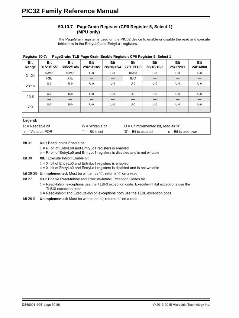
PIC32 Family Reference Manual
50.13.7 PageGrain Register (CP0 Register 5, Select 1) (MPU only)
The PageGrain register is used on the PIC32 device to enable or disable the read and executeinhibit bits in the EntryLo0 and EntryLo1 registers.
Register 50-7: PageGrain; TLB Page Grain Enable Register; CP0 Register 5, Select 1
Bit Range
Bit31/23/15/7
Bit30/22/14/6
Bit29/21/13/5
Bit28/20/12/4
Bit27/19/11/3
Bit26/18/10/2
Bit25/17/9/1
Bit24/16/8/0
31:24R/W-0 R/W-0 U-0 U-0 R/W-0 U-0 U-0 U-0
RIE XIE — — IEC — — —
23:16U-0 U-0 U-0 U-0 U-0 U-0 U-0 U-0
— — — — — — — —
15:8U-0 U-0 U-0 U-0 U-0 U-0 U-0 U-0
— — — — — — — —
7:0U-0 U-0 U-0 U-0 U-0 U-0 U-0 U-0
— — — — — — — —
Legend:
R = Readable bit W = Writable bit U = Unimplemented bit, read as ‘0’
-n = Value at POR ‘1’ = Bit is set ‘0’ = Bit is cleared x = Bit is unknown
bit 31 RIE: Read Inhibit Enable bit
1 = RI bit of EntryLo0 and EntryLo1 registers is enabled0 = RI bit of EntryLo0 and EntryLo1 registers is disabled and is not writable
bit 30 XIE: Execute Inhibit Enable bit
1 = XI bit of EntryLo0 and EntryLo1 registers is enabled0 = XI bit of EntryLo0 and EntryLo1 registers is disabled and is not writable
bit 29-28 Unimplemented: Must be written as ‘0’; returns ‘0’ on a read
bit 27 IEC: Enable Read-Inhibit and Execute-Inhibit Exception Codes bit
1 = Read-Inhibit exceptions use the TLBRI exception code. Execute-Inhibit exceptions use the TLBXI exception code
0 = Read-Inhibit and Execute-Inhibit exceptions both use the TLBL exception code
bit 26-0 Unimplemented: Must be written as ‘0’; returns ‘0’ on a read
DS60001192B-page 50-50 © 2013-2015 Microchip Technology Inc.

Section 50. CPU for Devices with MIPS32® microAptiv™ and M-Class Cores
50.13.8 Wired Register (CP0 Register 6, Select 0) (MPU Only)
The Wired register is a read/write register that specifies the boundary between the wired andrandom entries in the TLB. The width of the Wired field is calculated in the same manner as thatdescribed for the Index register. Wired entries are fixed, non-replaceable entries that are notoverwritten by a TLBWR instruction. Wired entries can be overwritten by a TLBWI instruction.
The Wired register is reset to zero by a Reset exception. Writing the Wired register causes theRandom register to reset to its upper bound.
Register 50-8: Wired; TLB Boundary Entries Register; CP0 Register 6, Select 0
Bit Range
Bit31/23/15/7
Bit30/22/14/6
Bit29/21/13/5
Bit28/20/12/4
Bit27/19/11/3
Bit26/18/10/2
Bit25/17/9/1
Bit24/16/8/0
31:24U-0 U-0 U-0 U-0 U-0 U-0 U-0 U-0
— — — — — — — —
23:16U-0 U-0 U-0 U-0 U-0 U-0 U-0 U-0
— — — — — — — —
15:8U-0 U-0 U-0 U-0 U-0 U-0 U-0 U-0
— — — — — — — —
7:0U-0 U-0 U-0 R/W-0 R/W-0 R/W-0 R/W-0 R/W-0
— — — Wired<4:0>(1)
Legend:
R = Readable bit W = Writable bit U = Unimplemented bit, read as ‘0’
-n = Value at POR ‘1’ = Bit is set ‘0’ = Bit is cleared x = Bit is unknown
bit 31-5 Unimplemented: Read as ‘0’
bit 4-0 Wired<4:0>: TLB Wired Boundary bits(1)
11111 = Entry 31 is random, entries 0-30 are wired•••
01111 = Entry 15 is random, entries 0-14 are wired•••00111 = Entries 7 and above are random, below 7 are wired•••
00000 = All 16 entries are random
Note 1: Depending on the configuration of the MMU, not all bits may be used. The number of TLB entries supported by the MMU can be read from the MMU Size<5:0> field of the Config1 CP0 register.
© 2013-2015 Microchip Technology Inc. DS60001192B-page 50-51

PIC32 Family Reference Manual
50.13.9 HWREna Register (CP0 Register 7, Select 0)
The HWREna register contains a bit mask that determines which hardware registers areaccessible through the RDHWR instruction.
Register 50-9: HWREna: Hardware Accessibility Register; CP0 Register 7, Select 0
Bit Range
Bit31/23/15/7
Bit30/22/14/6
Bit29/21/13/5
Bit28/20/12/4
Bit27/19/11/3
Bit26/18/10/2
Bit25/17/9/1
Bit24/16/8/0
31:24U-0 U-0 R/W-0 U-0 U-0 U-0 U-0 U-0
— — ULR — — — — —
23:16U-0 U-0 U-0 U-0 U-0 U-0 U-0 U-0
— — — — — — — —
15:8U-0 U-0 U-0 U-0 U-0 U-0 U-0 U-0
— — — — — — — —
7:0U-0 U-0 U-0 U-0 R/W-0 R/W-0 R/W-0 R/W-0
— — — — MASK<3:0>
Legend:
R = Readable bit W = Writable bit U = Unimplemented bit, read as ‘0’
-n = Value at POR ‘1’ = Bit is set ‘0’ = Bit is cleared x = Bit is unknown
bit 31-30 Unimplemented: Read as ‘0’
bit 29 ULR: User Local Register bit
1 = Enable unprivileged access to UserLocal register0 = Disable unprivileged access to UserLocal registerThis bit provides read access to the Coprocessor 0 UserLocal register.
bit 28-4 Unimplemented: Read as ‘0’
bit 3-0 MASK<3:0>: Bit Mask bits
1 = Access is enabled to corresponding hardware register 0 = Access is disabledEach of these bits enables access by the RDHWR instruction to a particular hardware register (which may not be an actual register). See the RDHWR instruction for a list of valid hardware registers.
DS60001192B-page 50-52 © 2013-2015 Microchip Technology Inc.

Section 50. CPU for Devices with MIPS32® microAptiv™ and M-Class Cores
50.13.10 BadVAddr Register (CP0 Register 8, Select 0)
BadVAddr is a read-only register that captures the most recent virtual address that caused anaddress error exception. Address errors are caused by executing load, store, or fetch operationsfrom unaligned addresses, or by trying to access Kernel mode addresses from User mode.
For devices with the MPU core, the BadVAddr register will also capture the most recent virtualaddress that caused a TLB refill, TLB invalid, or TLB modified exception.
BadVAddr does not capture address information for bus errors, because they are not addressingerrors.
Register 50-10: BadVAddr: Bad Virtual Address Register; CP0 Register 8, Select 0
Bit Range
Bit31/23/15/7
Bit30/22/14/6
Bit29/21/13/5
Bit28/20/12/4
Bit27/19/11/3
Bit26/18/10/2
Bit25/17/9/1
Bit24/16/8/0
31:24R-x R-x R-x R-x R-x R-x R-x R-x
BadVAddr<31:24>
23:16R-x R-x R-x R-x R-x R-x R-x R-x
BadVAddr<23:16>
15:8R-x R-x R-x R-x R-x R-x R-x R-x
BadVAddr<15:8>
7:0R-x R-x R-x R-x R-x R-x R-x R-x
BadVAddr<7:0>
Legend:
R = Readable bit W = Writable bit U = Unimplemented bit, read as ‘0’
-n = Value at POR ‘1’ = Bit is set ‘0’ = Bit is cleared x = Bit is unknown
bit 31-0 BadVAddr<31:0>: Bad Virtual Address bits
Captures the virtual address that caused the most recent address error exception.
© 2013-2015 Microchip Technology Inc. DS60001192B-page 50-53

PIC32 Family Reference Manual
50.13.11 BadInstr Register (CP0 Register 8, Select 1) (M-Class only)
The BadInstr register is an optional read-only register that captures the most recent instructionthat caused one of the following exceptions:
• Instruction Validity: Coprocessor Unusable, Reserved Instruction
• Execution Exception: Integer Overflow, Trap, System Call, Breakpoint, Floating-point, Coprocessor 2 exception
• Addressing: Address Error, TLB Refill, TLB Invalid, TLB Read Inhibit, TLB Execute Inhibit, TLB Modified
The BadInstr register is provided to allow acceleration of instruction emulation. The BadInstr reg-ister is only set by exceptions that are synchronous to an instruction. The BadInstr register is notset by Interrupts or by NMI, Machine check, Bus Error, Cache Error, Watch, or EJTAG excep-tions.
When a synchronous exception occurs for which there is no valid instruction word (for exampleTLB Refill - Instruction Fetch), the value stored in BadInstr is unpredictable.
Presence of the BadInstr register is indicated by the Config3BI bit. The BadInstr register is instan-tiated per-VPE in an MT ASE processor.
Register 50-11: BadInstr: Bad Instruction Word Register; CP0 Register 8, Select 1
Bit Range
Bit31/23/15/7
Bit30/22/14/6
Bit29/21/13/5
Bit28/20/12/4
Bit27/19/11/3
Bit26/18/10/2
Bit25/17/9/1
Bit24/16/8/0
31:24R-x R-x R-x R-x R-x R-x R-x R-x
BadInstr<31:24>
23:16R-x R-x R-x R-x R-x R-x R-x R-x
BadInstr<23:16>
15:8R-x R-x R-x R-x R-x R-x R-x R-x
BadInstr<15:8>
7:0R-x R-x R-x R-x R-x R-x R-x R-x
BadInstr<7:0>
Legend:
R = Readable bit W = Writable bit U = Unimplemented bit, read as ‘0’
-n = Value at POR ‘1’ = Bit is set ‘0’ = Bit is cleared x = Bit is unknown
bit 31-0 BadInstr<31:0>: Bad (Faulting) Instruction Word bits
Instruction words smaller than 32 bits are placed in bits 15:0, with bits 31:16 containing ‘0’.
DS60001192B-page 50-54 © 2013-2015 Microchip Technology Inc.

Section 50. CPU for Devices with MIPS32® microAptiv™ and M-Class Cores
50.13.12 BadInstrP Register (CP0 Register 8, Select 2) (M-Class only)
The BadInstrP register is an optional register that is used in conjunction with the BadInstrregister. The BadInstrP register contains the prior branch instruction when the faulting instructionis in a branch delay slot.
The BadInstrP register is updated for these exceptions:
• Instruction Validity: Coprocessor Unusable, Reserved Instruction
• Execution Exception: Integer Overflow, Trap, System Call, Breakpoint, Floating-point, Coprocessor 2 exception
• Addressing: Address Error, TLB Refill, TLB Invalid, TLB Read Inhibit, TLB Execute Inhibit, TLB Modified
The BadInstrP register is provided to allow acceleration of instruction emulation. The BadInstrPregister is only set by exceptions that are synchronous to an instruction. The BadInstrP registeris not set by Interrupts or by NMI, Machine check, Bus Error, Cache Error, Watch, or EJTAGexceptions. When a synchronous exception occurs, and the faulting instruction is not in a branchdelay slot, then the value stored in BadInstrP is unpredictable.
Presence of the BadInstrP register is indicated by the Config3BP bit. The BadInstrP register isinstantiated per-VPE in an MT ASE processor.
Register 50-12: BadInstrP: Bad Prior Branch Instruction Register; CP0 Register 8, Select 2
Bit Range
Bit31/23/15/7
Bit30/22/14/6
Bit29/21/13/5
Bit28/20/12/4
Bit27/19/11/3
Bit26/18/10/2
Bit25/17/9/1
Bit24/16/8/0
31:24R-x R-x R-x R-x R-x R-x R-x R-x
BadInstrP<31:24>
23:16R-x R-x R-x R-x R-x R-x R-x R-x
BadInstrP<23:16>
15:8R-x R-x R-x R-x R-x R-x R-x R-x
BadInstrP<15:8>
7:0R-x R-x R-x R-x R-x R-x R-x R-x
BadInstrP<7:0>
Legend:
R = Readable bit W = Writable bit U = Unimplemented bit, read as ‘0’
-n = Value at POR ‘1’ = Bit is set ‘0’ = Bit is cleared x = Bit is unknown
bit 31-0 BadInstrP<31:0>: Bad Prior Branch Instruction bits
Instruction words smaller than 32 bits are placed in bits 15:0, with bits 31:16 containing ‘0’.
© 2013-2015 Microchip Technology Inc. DS60001192B-page 50-55

PIC32 Family Reference Manual
50.13.13 Count Register (CP0 Register 9, Select 0)
The Count register acts as a timer, incrementing at a constant rate, whether or not an instructionis executed, retired, or any forward progress is made through the pipeline. The counterincrements every other clock, if the DC bit in the Cause register is ‘0’.
Count can be written for functional or diagnostic purposes, including at Reset or to synchronizeprocessors.
By writing the COUNTDM bit in the Debug register, it is possible to control whether Countcontinues to increment while the processor is in Debug mode.
Register 50-13: Count: Interval Counter Register; CP0 Register 9, Select 0
Bit Range
Bit31/23/15/7
Bit30/22/14/6
Bit29/21/13/5
Bit28/20/12/4
Bit27/19/11/3
Bit26/18/10/2
Bit25/17/9/1
Bit24/16/8/0
31:24R/W-x R/W-x R/W-x R/W-x R/W-x R/W-x R/W-x R/W-x
COUNT<31:24>
23:16R/W-x R/W-x R/W-x R/W-x R/W-x R/W-x R/W-x R/W-x
COUNT<23:16>
15:8R/W-x R/W-x R/W-x R/W-x R/W-x R/W-x R/W-x R/W-x
COUNT<15:8>
7:0R/W-x R/W-x R/W-x R/W-x R/W-x R/W-x R/W-x R/W-x
COUNT<7:0>
Legend:
R = Readable bit W = Writable bit U = Unimplemented bit, read as ‘0’
-n = Value at POR ‘1’ = Bit is set ‘0’ = Bit is cleared x = Bit is unknown
bit 31-0 COUNT<31:0>: Interval Counter bits
This value is incremented every other clock cycle.
DS60001192B-page 50-56 © 2013-2015 Microchip Technology Inc.

Section 50. CPU for Devices with MIPS32® microAptiv™ and M-Class Cores
50.13.14 EntryHi Register (CP0 Register 10, Select 0) (MPU only)
The EntryHi register contains the virtual address match information used for TLB read, write, andaccess operations.
A TLB exception (TLB Refill, TLB Invalid, or TLB Modified) causes bits VA31...13 of the virtualaddress to be written into the VPN2 field of the EntryHi register. A TLBR instruction writes theEntryHi register with the corresponding fields from the selected TLB entry. The ASID field iswritten by software with the current address space identifier value and is used during the TLBcomparison process to determine TLB match.
Because the ASID field is overwritten by a TLBR instruction, software must save and restore thevalue of ASID around use of the TLBR. This is especially important in TLB Invalid and TLBModified exceptions, and in other memory management software.
The VPN2 field of the EntryHi register is not defined after an address error exception, and maybe modified by hardware during the address error exception sequence. Software writes of theEntryHi register (via MTC0) do not cause the implicit write of address-related fields in theBadVAddr or Context registers.
Register 50-14: EntryHi: TLB Address Match Register; CP0 Register 10, Select 0
Bit Range
Bit31/23/15/7
Bit30/22/14/6
Bit29/21/13/5
Bit28/20/12/4
Bit27/19/11/3
Bit26/18/10/2
Bit25/17/9/1
Bit24/16/8/0
31:24R/W-x R/W-x R/W-x R/W-x R/W-x R/W-x R/W-x R/W-x
VPN2<18:11>
23:16R/W-x R/W-x R/W-x R/W-x R/W-x R/W-x R/W-x R/W-x
VPN2<10:3>
15:8R/W-x R/W-x R/W-x U-0 U-0 U-0 U-0 U-0
VPN2<2:0> — — — — —
7:0R/W-x R/W-x R/W-x R/W-x R/W-x R/W-x R/W-x R/W-x
ASID<7:0>
Legend:
R = Readable bit W = Writable bit U = Unimplemented bit, read as ‘0’
-n = Value at POR ‘1’ = Bit is set ‘0’ = Bit is cleared x = Bit is unknown
bit 31-13 VPN2<18:11>: Virtual Page Number bitsThese bits are written by hardware on a TLB exception or on a TLB read, and are written by software beforea TLB write.
bit 12-8 Unimplemented: Read as ‘0’
bit 7-0 ASID<7:0>: Address Space Identifier bitsThese bits are written by hardware on a TLB read and by software to establish the current ASID value for a TLB write and against which TLB references match each entry’s TLB ASID field.
© 2013-2015 Microchip Technology Inc. DS60001192B-page 50-57

PIC32 Family Reference Manual
50.13.15 Compare Register (CP0 Register 11, Select 0)
The Compare register acts in conjunction with the Count register to implement a timer and timerinterrupt function. Compare maintains a stable value and does not change on its own.
When the value of Count equals the value of Compare, the CPU asserts an interrupt signal to thesystem interrupt controller. This signal will remain asserted until Compare is written.
Register 50-15: Compare: Interval Count Compare Register; CP0 Register 11, Select 0
Bit Range
Bit31/23/15/7
Bit30/22/14/6
Bit29/21/13/5
Bit28/20/12/4
Bit27/19/11/3
Bit26/18/10/2
Bit25/17/9/1
Bit24/16/8/0
31:24R/W-x R/W-x R/W-x R/W-x R/W-x R/W-x R/W-x R/W-x
COMPARE<31:24>
23:16R/W-x R/W-x R/W-x R/W-x R/W-x R/W-x R/W-x R/W-x
COMPARE<23:16>
15:8R/W-x R/W-x R/W-x R/W-x R/W-x R/W-x R/W-x R/W-x
COMPARE<15:8>
7:0R/W-x R/W-x R/W-x R/W-x R/W-x R/W-x R/W-x R/W-x
COMPARE<7:0>
Legend:
R = Readable bit W = Writable bit U = Unimplemented bit, read as ‘0’
-n = Value at POR ‘1’ = Bit is set ‘0’ = Bit is cleared x = Bit is unknown
bit 31-0 COMPARE<31:0>: Interval Count Compare Value bits
DS60001192B-page 50-58 © 2013-2015 Microchip Technology Inc.

Section 50. CPU for Devices with MIPS32® microAptiv™ and M-Class Cores
50.13.16 Status Register (CP0 Register 12, Select 0)
The read/write Status register contains the operating mode, interrupt enabling, and the diagnosticstates of the processor. The bits of this register combine to create operating modes for the processor.
50.13.16.1 INTERRUPT ENABLE
Interrupts are enabled when all of the following conditions are true:
• IE = 1• EXL = 0• ERL = 0• DM = 0
If these conditions are met, the settings of the IPL bits enable the interrupts.
50.13.16.2 OPERATING MODES
If the DM bit in the Debug register is ‘1’, the processor is in Debug mode; otherwise, theprocessor is in either Kernel mode or User mode. The CPU Status register bit settings shown inTable 50-25 determine User or Kernel mode:
Table 50-25: CPU Status Register Bits That Determine Processor Mode
Mode Bit/Setting
User (requires all of the following bits and values) UM = 1 EXL = 0 ERL = 0
Kernel (requires one or more of the following bit values) UM = 0 EXL = 1 ERL = 1
Note: The Status register CU0 bit (Status<28>) controls Coprocessor 0 accessibility. IfCoprocessor 0 is unusable, an instruction that accesses it generates an exception.
Register 50-16: Status: Status Register; CP0 Register 12, Select 0
Bit Range
Bit31/23/15/7
Bit30/22/14/6
Bit29/21/13/5
Bit28/20/12/4
Bit27/19/11/3
Bit26/18/10/2
Bit25/17/9/1
Bit24/16/8/0
31:24U-0 U-0 R/W-0 R/W-x R/W-0 R/W-0 R/W-x R/W-0
— — CU1(2) CU0 RP FR(2) RE MX(3)
23:16U-0 R/W-1 R/W-0, HS, CS R/W-1 R/W-0 R/W-x U-0 R/W-0
— BEV TS(1) SR NMI IPL<7> — IPL<6>
15:8R/W-x R/W-x R/W-x R/W-x R/W-x R/W-x U-0 U-0
IPL<5:0> — —
7:0U-0 U-0 U-0 R/W-x U-0 R/W-x R/W-x R/W-x
— — — UM — ERL EXL IE
Legend: HS = Set by hardware CS = Cleared by software
R = Readable bit W = Writable bit U = Unimplemented bit, read as ‘0’
-n = Value at POR ‘1’ = Bit is set ‘0’ = Bit is cleared x = Bit is unknown
bit 31-30 Unimplemented: Read as ‘0’
Note 1: This bit is only available on devices with the MPU core. Refer to the “CPU” chapter in the specific device data sheet for availability.
2: This bit is only available on devices with the M-Class core. Refer to the specific device data sheet for availability.
3: DSP ASE is not available on all devices. Refer to the “CPU” chapter in the specific device data sheet for availability.
© 2013-2015 Microchip Technology Inc. DS60001192B-page 50-59

PIC32 Family Reference Manual
bit 29 CU1: Coprocessor 1 Usable bit(2)
This bit allows access to Coprocessor 1. This bit can only be written if the FPU is configured. This bit will read as ‘0’ if the FPU is not present.1 = Access is allowed0 = Access is not allowed
bit 28 CU0: Coprocessor 0 Usable bitThis bit controls access to Coprocessor 0.1 = Access is allowed0 = Access is not allowedCoprocessor 0 is always usable when the processor is running in Kernel mode, independent of the state ofthe CU0 bit.
bit 27 RP: Reduced Power bit1 = Enables Reduced Power mode0 = Disables Reduced Power mode
bit 26 FR: Floating Point Register Mode(2)
1 = Floating-point registers can contain any data type0 = Floating-point registers can contain any 32-bit data type. 64-bit data types are stored in even-odd pairs
of registers
Note: This bit must be ignored on write and read as ‘0’ for CPUs with no FPU.
bit 25 RE: Reverse-endian Memory Reference Enable bitUsed to enable reverse-endian memory references while the processor is running in User mode1 = User mode uses reversed endianness0 = User mode uses configured endiannessDebug, Kernel, or Supervisor mode references are not affected by the state of this bit.
bit 24 MX: MIPS DSP Resource Enable bit(3)
This bit must be set prior to executing any DSP ASE instruction. An attempt to execute a DSP ASE instruction while this bit is cleared will result in a DSP State Disabled exception.1 = Access is enabled0 = Access is disabled
bit 23 Unimplemented: Read as ‘0’
bit 22 BEV: Bootstrap Exception Vector Control bitControls the location of exception vectors.1 = Bootstrap0 = Normal
bit 21 TS: TLB Shutdown Control bit(1)
Indicates that the TLB has detected a match on multiple entries. This bit is also set if a TLBWI or TLBWRinstruction is issued that would cause a TLB shutdown condition if allowed to complete. A machine checkexception is also issued.
1 = TLB shutdown event
0 = No TLB shutdown event
Software can only write a '0' to this bit to clear it and cannot force a '0' to '1' transition.
bit 20 SR: Soft Reset bitIndicates that the entry through the Reset exception vector was due to a Soft Reset.
1 = Soft Reset; this bit is always set for any type of reset on the PIC32 core0 = Not used on PIC32Software can only write a ‘0’ to this bit to clear it and cannot force a ‘0’ to ‘1’ transition.
Register 50-16: Status: Status Register; CP0 Register 12, Select 0 (Continued)
Note 1: This bit is only available on devices with the MPU core. Refer to the “CPU” chapter in the specific device data sheet for availability.
2: This bit is only available on devices with the M-Class core. Refer to the specific device data sheet for availability.
3: DSP ASE is not available on all devices. Refer to the “CPU” chapter in the specific device data sheet for availability.
DS60001192B-page 50-60 © 2013-2015 Microchip Technology Inc.
Section 50. CPU for Devices with MIPS32® microAptiv™ and M-Class Cores
bit 19 NMI: Non-Maskable Interrupt bitIndicates that the entry through the reset exception vector was due to a NMI.
1 = NMI0 = Not NMI (Soft Reset or Reset)Software can only write a ‘0’ to this bit to clear it and cannot force a ‘0’ to ‘1’ transition.
bit 18 IPL<7>: Interrupt Priority Level bitsThis field is the encoded (0-256) value of the current IPL. An interrupt will be signaled only if the requestedIPL is higher than this value.
bit 17 Unimplemented: Read as ‘0’
bit 16-10 IPL<6:0>: Interrupt Priority Level bitsThis field is the encoded (0-256) value of the current IPL. An interrupt will be signaled only if the requestedIPL is higher than this value.
bit 9-5 Unimplemented: Read as ‘0’
bit 4 UM: User Mode bitThis bit denotes the base operating mode of the processor. On the encoding of this bit is:1 = Base mode is User mode0 = Base mode in Kernel modeThe processor can also be in Kernel mode if ERL or EXL is set, regardless of the state of the UM bit.
bit 3 Unimplemented: Read as ‘0’
bit 2 ERL: Error Level bitSet by the processor when a Reset, Soft Reset, NMI or Cache Error exception are taken.1 = Error level0 = Normal levelWhen ERL is set:
• Processor is running in Kernel mode
• Interrupts are disabled
• ERET instruction will use the return address held in the ErrorEPC register instead of the EPC register
• Lower 229 bytes of kuseg are treated as an unmapped and uncached region. This allows main mem-ory to be accessed in the presence of cache errors. The operation of the processor is undefined if the ERL bit is set while the processor is executing instructions from kuseg.
bit 1 EXL: Exception Level bitSet by the processor when any exception other than Reset, Soft Reset, or NMI exceptions is taken.1 = Exception level0 = Normal level
When EXL is set:
• Processor is running in Kernel mode
• Interrupts are disabled
EPC, BD, and SRSCtl will not be updated if another exception is taken.
bit 0 IE: Interrupt Enable bitActs as the master enable for software and hardware interrupts:1 = Interrupts are enabled0 = Interrupts are disabledThis bit may be modified separately via the DI and EI instructions
Register 50-16: Status: Status Register; CP0 Register 12, Select 0 (Continued)
Note 1: This bit is only available on devices with the MPU core. Refer to the “CPU” chapter in the specific device data sheet for availability.
2: This bit is only available on devices with the M-Class core. Refer to the specific device data sheet for availability.
3: DSP ASE is not available on all devices. Refer to the “CPU” chapter in the specific device data sheet for availability.
© 2013-2015 Microchip Technology Inc. DS60001192B-page 50-61

PIC32 Family Reference Manual
50.13.17 IntCtl: Interrupt Control Register (CP0 Register 12, Select 1)
The IntCtl register controls the vector spacing of the PIC32 architecture.
Register 50-17: IntCtl: Interrupt Control Register; CP0 Register 12, Select 1
Bit Range
Bit31/23/15/7
Bit30/22/14/6
Bit29/21/13/5
Bit28/20/12/4
Bit27/19/11/3
Bit26/18/10/2
Bit25/17/9/1
Bit24/16/8/0
31:24U-0 U-0 U-0 U-0 U-0 U-0 U-0 U-0
— — — — — — — —
23:16U-0 R/W-0 R/W-0 R/W-0 R/W-0 R/W-0 R/W-1 R/W-1
— PF ICE STKDEC<4:0>
15:8R/W-0 R/W-0 R/W-0 U-0 U-0 U-0 R/W-0 R/W-0
CLREXL APE USESTK — — — VS<4:3>
7:0R/W-0 R/W-0 R/W-0 U-0 U-0 U-0 U-0 U-0
VS<2:0> — — — — —
Legend:
R = Readable bit W = Writable bit U = Unimplemented bit, read as ‘0’
-n = Value at POR ‘1’ = Bit is set ‘0’ = Bit is cleared x = Bit is unknown
bit 31-23 Unimplemented: Read as ‘0’
bit 22 PF: Vector Prefetching Enable bit
1 = Vector Prefetching is Enabled0 = Vector Prefetching is Disabled
bit 21 ICE: Interrupt Chaining Enable bit
1 = Interrupt chaining is Enabled0 = Interrupt chaining is Disabled
bit 20-16 STKDEC<4:0>: Stack Pointer Decrement bits
For the Auto-Prologue feature, this is the number of 4-byte words that are decremented from the stack pointer value.31-4 = Specifies the number of words to be decremented3-0 = Decrement 3 words (12 bytes)
bit 15 CLREXL: Clear KSU/ERL/EXL bit
For the Auto-Prologue feature and IRET instruction, this bit, if set, during Auto-Prologue and IRET interrupt chaining, clears the KSU/ERL/EXL bits.1 = Bits are cleared by these operations0 = Bits are not cleared by these operations
bit 14 APE: Auto-Prologue Enable bit
1 = Auto-Prologue is enabled0 = Auto-Prologue is disabled
bit 13 USEKSTK: Stack Use bit
Chooses which Stack to use during Interrupt Auto-Prologue.1 = Use r29 of the Current SRS at the beginning of IAPUsed for environments where there are separate User mode and Kernel mode stacks. In this case, r29 of the SRS used during IAP must be preinitialized by software to hold the Kernel mode stack pointer.0 = Copy r29 of the Previous SRS to the Current SRS at the beginning of IAPUsed for Bare-Iron environments with only one stack.
bit 12-10 Unimplemented: Read as ‘0’
DS60001192B-page 50-62 © 2013-2015 Microchip Technology Inc.

Section 50. CPU for Devices with MIPS32® microAptiv™ and M-Class Cores
bit 9-5 VS<4:0>: Vector Spacing bits
These bits specify the spacing between each interrupt vector.
All other values are reserved. The operation of the processor is undefined if a reserved value is written to these bits.
bit 4-0 Unimplemented: Read as ‘0’
Register 50-17: IntCtl: Interrupt Control Register; CP0 Register 12, Select 1 (Continued)
Encoding Spacing Between Vectors (hex) Spacing Between Vectors (decimal)
0x00 0x000 0
0x01 0x020 32
0x02 0x040 64
0x04 0x080 128
0x08 0x100 256
0x10 0x200 512
© 2013-2015 Microchip Technology Inc. DS60001192B-page 50-63

PIC32 Family Reference Manual
50.13.18 SRSCtl Register (CP0 Register 12, Select 2)
The SRSCtl register controls the operation of GPR shadow sets in the processor.
Table 50-26: Sources for New CSS on an Exception or Interrupt
Exception Type Bit Source Condition Comment
Exception ESS All —
Non-Vectored Interrupt ESS IV bit = 0 (Cause<23>) Treat as exception
Vectored EIC Interrupt EICSS IV bit = 1 (Cause<23>) and, VEIC bit = 1 (Config3<6>)
Source is external interrupt controller.
Register 50-18: SRSCtl: Shadow Register Set Register; CP0 Register 12, Select 2
Bit Range
Bit31/23/15/7
Bit30/22/14/6
Bit29/21/13/5
Bit28/20/12/4
Bit27/19/11/3
Bit26/18/10/2
Bit25/17/9/1
Bit24/16/8/0
31:24U-0 U-0 R-0 R-1 R-1 R-1 U-0 U-0
— — HSS<3:0> — —
23:16U-0 U-0 R-x R-x R-x R-x U-0 U-0
— — EICSS<3:0> — —
15:8R/W-0 R/W-0 R/W-0 R/W-0 U-0 U-0 R/W-0 R/W-0
ESS<3:0> — — PSS<3:2>
7:0R/W-0 R/W-0 U-0 U-0 R-0 R-0 R-0 R-0
PSS<1:0> — — CSS<3:0>
Legend:
R = Readable bit W = Writable bit U = Unimplemented bit, read as ‘0’
-n = Value at POR ‘1’ = Bit is set ‘0’ = Bit is cleared x = Bit is unknown
bit 31-30 Unimplemented: Read as ‘0’
bit 29-26 HSS<3:0>: High Shadow Set bits
This bit contains the highest shadow set number that is implemented by this processor. A value of ‘0000’ in these bits indicates that only the normal GPRs are implemented.1111 = Reserved0111 = Eight shadow sets are present0110 = Reserved0101 = Reserved0100 = Reserved0011 = Four shadow sets are present0010 = Reserved0001 = Two shadow sets are present0000 = One shadow set (normal GPR set) is presentThe value in this bit also represents the highest value that can be written to the ESS<3:0>, EICSS<3:0>, PSS<3:0>, and CSS<3:0> bits of this register, or to any of the bits of the SRSMap register. The operation of the processor is undefined if a value larger than the one in this bit is written to any of these other bits.
bit 25-22 Unimplemented: Read as ‘0’
bit 21-18 EICSS<3:0>: External Interrupt Controller Shadow Set bits
EIC Interrupt mode shadow set. This bit is loaded from the external interrupt controller for each interrupt request and is used in place of the SRSMap register to select the current shadow set for the interrupt.
bit 17-16 Unimplemented: Read as ‘0’
bit 15-12 ESS<3:0>: Exception Shadow Set bits
This bit specifies the shadow set to use on entry to Kernel mode caused by any exception other than a vectored interrupt. The operation of the processor is undefined if software writes a value into this bit that is greater than the value in the HSS<3:0> bits.
bit 11-10 Unimplemented: Read as ‘0’
DS60001192B-page 50-64 © 2013-2015 Microchip Technology Inc.

Section 50. CPU for Devices with MIPS32® microAptiv™ and M-Class Cores
bit 9-6 PSS<3:0>: Previous Shadow Set bits
Since GPR shadow registers are implemented, this bit is copied from the CSS bit when an exception or interrupt occurs. An ERET instruction copies this value back into the CSS bit if the BEV bit (Status<22>) = 0.
This bit is not updated on any exception which sets the ERL bit (Status<2>) to ‘1’ (i.e., Reset, Soft Reset,NMI, cache error), an entry into EJTAG Debug mode, or any exception or interrupt that occurs with the EXLbit (Status<1>) = 1, or BEV = 1. This bit is not updated on an exception that occurs while ERL = 1.
The operation of the processor is undefined if software writes a value into this bit that is greater than thevalue in the HSS<3:0> bits.
bit 5-4 Unimplemented: Read as ‘0’
bit 3-0 CSS<3:0>: Current Shadow Set bits
Since GPR shadow registers are implemented, this bit is the number of the current GPR set. This bit isupdated with a new value on any interrupt or exception, and restored from the PSS bit on an ERET.
Table 50-26 describes the various sources from which the CSS<3:0> bits are updated on an exception orinterrupt.
This bit is not updated on any exception which sets the ERL bit (Status<2>) to ‘1’ (i.e., Reset, Soft Reset,NMI, cache error), an entry into EJTAG Debug mode, or any exception or interrupt that occurs with EXL bit(Status<1>) = 1, or BEV = 1. Neither is it updated on an ERET with ERL = 1 or BEV = 1. This bit is notupdated on an exception that occurs while ERL = 1.
The value of the CSS<3:0> bits can be changed directly by software only by writing the PSS<3:0> bits andexecuting an ERET instruction.
Register 50-18: SRSCtl: Shadow Register Set Register; CP0 Register 12, Select 2 (Continued)
© 2013-2015 Microchip Technology Inc. DS60001192B-page 50-65

PIC32 Family Reference Manual
50.13.19 SRSMap: Register (CP0 Register 12, Select 3)
The SRSMap register contains eight 4-bit fields that provide the mapping from a vector numberto the shadow set number to use when servicing such an interrupt. The values from this registerare not used for a non-interrupt exception, or a non-vectored interrupt (IV bit = 0, Cause<23> orVS<4:0> bit = 0, IntCtl<9:5>). In such cases, the shadow set number comes from the ESS<3:0>bits (SRSCtl<15:12>).
If the HSS<3:0> bits (SRSCTL29:26) are ‘0’, the results of a software read or write of this registerare unpredictable.
The operation of the processor is undefined if a value is written to any bit in this register that isgreater than the value of the HSS<3:0> bits.
The SRSMap register contains the shadow register set numbers for vector numbers 7-0. Thesame shadow set number can be established for multiple interrupt vectors, creating amany-to-one mapping from a vector to a single shadow register set number.
Register 50-19: SRSMap: Shadow Register Set Map Register; CP0 Register 12, Select 3
Bit Range
Bit31/23/15/7
Bit30/22/14/6
Bit29/21/13/5
Bit28/20/12/4
Bit27/19/11/3
Bit26/18/10/2
Bit25/17/9/1
Bit24/16/8/0
31:24R/W-0 R/W-0 R/W-0 R/W-0 R/W-0 R/W-0 R/W-0 R/W-0
SSV7<3:0> SSV6<3:0>
23:16R/W-0 R/W-0 R/W-0 R/W-0 R/W-0 R/W-0 R/W-0 R/W-0
SSV5<3:0> SSV4<3:0>
15:8R/W-0 R/W-0 R/W-0 R/W-0 R/W-0 R/W-0 R/W-0 R/W-0
SSV3<3:0> SSV2<3:0>
7:0R/W-0 R/W-0 R/W-0 R/W-0 R/W-0 R/W-0 R/W-0 R/W-0
SSV1<3:0> SSV0<3:0>
Legend:
R = Readable bit W = Writable bit U = Unimplemented bit, read as ‘0’
-n = Value at POR ‘1’ = Bit is set ‘0’ = Bit is cleared x = Bit is unknown
bit 31-28 SSV7<3:0>: Shadow Set Vector 7 bits
Shadow register set number for Vector Number 7.
bit 27-24 SSV6<3:0>: Shadow Set Vector 6 bits
Shadow register set number for Vector Number 6.
bit 23-20 SSV5<3:0>: Shadow Set Vector 5 bits
Shadow register set number for Vector Number 5.
bit 19-16 SSV4<3:0>: Shadow Set Vector 4 bits
Shadow register set number for Vector Number 4.
bit 15-12 SSV3<3:0>: Shadow Set Vector 3 bits
Shadow register set number for Vector Number 3.
bit 11-8 SSV2<3:0>: Shadow Set Vector 2 bits
Shadow register set number for Vector Number 2.
bit 7-4 SSV1<3:0>: Shadow Set Vector 1 bits
Shadow register set number for Vector Number 1.
bit 3-0 SSV0<3:0>: Shadow Set Vector 0 bit
Shadow register set number for Vector Number 0.
DS60001192B-page 50-66 © 2013-2015 Microchip Technology Inc.

Section 50. CPU for Devices with MIPS32® microAptiv™ and M-Class Cores
50.13.20 View_IPL Register (CP0 Register 12, Select 4)
This register gives read and write access to the IPL<7:0> bits that are also available in the Statusregister. The use of this register allows the Priority Level to be read/written withoutextracting/inserting that field from/to the Status register.
The IPL field is located in non-contiguous bits within the Status register. All of the IPL bits arepresented as a contiguous field within this register.
Register 50-20: View_IPL: View Interrupt Priority Level Register; CP0 Register 12, Select 4
Bit Range
Bit31/23/15/7
Bit30/22/14/6
Bit29/21/13/5
Bit28/20/12/4
Bit27/19/11/3
Bit26/18/10/2
Bit25/17/9/1
Bit24/16/8/0
31:24U-0 U-0 U-0 U-0 U-0 U-0 U-0 U-0
— — — — — — — —
23:16U-0 U-0 U-0 U-0 U-0 U-0 U-0 U-0
— — — — — — — —
15:8U-0 U-0 U-0 U-0 U-0 U-0 R/W-0 R/W-0
— — — — — — IPL<7:6>
7:0R/W-0 R/W-0 R/W-0 R/W-0 R/W-0 R/W-0 U-0 U-0
IPL<5:0> — —
Legend:
R = Readable bit W = Writable bit U = Unimplemented bit, read as ‘0’
-n = Value at POR ‘1’ = Bit is set ‘0’ = Bit is cleared x = Bit is unknown
bit 31-10 Unimplemented: Read as ‘0’
bit 9-2 IPL<7:0>: These bits contain the encoded (0...256) value of the current IPL.
bit 1-0 Unimplemented: Read as ‘0’
© 2013-2015 Microchip Technology Inc. DS60001192B-page 50-67

PIC32 Family Reference Manual
50.13.21 SRSMAP2 Register (CP0 Register 12, Select 5)
The SRSMAP2 register contains two 4-bit bits that provide the mapping from an vector numberto the shadow set number to use when servicing such an interrupt. The values from this registerare not used for a non-interrupt exception, or a non-vectored interrupt (IV bit (Cause<23>) = 0or the VS<4:0> bits (IntCtl<9:5>) = 0). In such cases, the shadow set number comes from theESS<3:0> bits (SRSCtl<15:12>).
If the HSS<3:0> bits (SRSCtl<9:6>) are ‘0’, the results of a software read or write of this registerare unpredictable.
The operation of the processor is undefined if a value is written to any bit in this register that is greater than the value of the HSS<3:0> bits.
The SRSMAP2 register contains the shadow register set numbers for vector numbers 9:8. Thesame shadow set number can be established for multiple interrupt vectors, creating amany-to-one mapping from a vector to a single shadow register set number.
Register 50-21: SRSMAP2: Shadow Register Set Map 2 Register; CP0 Register 12, Select 5
Bit Range
Bit31/23/15/7
Bit30/22/14/6
Bit29/21/13/5
Bit28/20/12/4
Bit27/19/11/3
Bit26/18/10/2
Bit25/17/9/1
Bit24/16/8/0
31:24U-0 U-0 U-0 U-0 U-0 U-0 U-0 U-0
— — — — — — — —
23:16U-0 U-0 U-0 U-0 U-0 U-0 U-0 U-0
— — — — — — — —
15:8U-0 U-0 U-0 U-0 U-0 U-0 U-0 U-0
— — — — — — — —
7:0R/W-x R/W-x R/W-x R/W-x R/W-x R/W-x R/W-x R/W-x
SSV9<3:0> SSV8<3:0>
Legend:
R = Readable bit W = Writable bit U = Unimplemented bit, read as ‘0’
-n = Value at POR ‘1’ = Bit is set ‘0’ = Bit is cleared x = Bit is unknown
bit 31-8 Unimplemented: Read as ‘0’
bit 7-4 SSV9<3:0>: Shadow Set Vector 9 bits
Shadow register set number for Vector Number 9.
bit 3-0 SSV8<3:0>: Shadow Set Vector 8 bits
Shadow register set number for Vector Number 8.
DS60001192B-page 50-68 © 2013-2015 Microchip Technology Inc.

Section 50. CPU for Devices with MIPS32® microAptiv™ and M-Class Cores
50.13.22 Cause Register (CP0 Register 13, Select 0)
The Cause register primarily describes the cause of the most recent exception. In addition, bitsalso control software interrupt requests and the vector through which interrupts are dispatched.With the exception of the IP1, IP0, DC, and IV bits, all bits in the Cause register are read-only.
Table 50-27: Cause Register EXCCODE<4:0> Bits
Exception Code ValueMnemonic Description
Decimal Hex
0 0x00 Int Interrupt
1 0x01 MOD(1) TLB modified exception
2 0x02 TLBL(1) TLB exception (load or instruction fetch)
3 0x03 TLBS(1) TLB exception (store)
4 0x04 AdEL Address error exception (load or instruction fetch)
5 0x05 AdES Address error exception (store)
6 0x06 IBE Bus error exception (instruction fetch)
7 0x07 DBE Bus error exception (data reference: load or store)
8 0x08 Sys Syscall exception
9 0x09 Bp Breakpoint exception
10 0x0a RI Reserved instruction exception
11 0x0B CPU Coprocessor Unusable exception
12 0x0C Ov Arithmetic Overflow exception
13 0x0D Tr Trap exception
14 0x0E — Reserved
15 0x0F FPE(2) Floating Point exception
16-18 0x10-0x0x12 Reserved
19 0x13 TLBRI(1)I TLB read-inhibit
20 0x14 TLBEI(1) TLB execute-inhibit
21-22 0x15-0x16 — Reserved
23 0x17 WATCH(1) Reference to WatchHi/WatchLo address
24 0x18 MCheck(1) Machine check
25 0x19 — Reserved
26 0x1A DSPDis DSP ASE state disabled exception(3)
27-31 0x1B-0x1F — Reserved
Note 1: This feature is only available on PIC32 devices with the MPU core. Refer to the “CPU” chapter in the specific device data sheet for availability.
2: This feature is only available on PIC32 devices with the M-Class core. Refer to the “FPU” chapter in the specific device data sheet to determine availability.
3: DSP ASE is not available on all devices. Please consult the “CPU” chapter of the specific device data sheet to determine availability
© 2013-2015 Microchip Technology Inc. DS60001192B-page 50-69

PIC32 Family Reference Manual
Register 50-22: Cause: Exception Cause Register; CP0 Register 13, Select 0
Bit Range
Bit31/23/15/7
Bit30/22/14/6
Bit29/21/13/5
Bit28/20/12/4
Bit27/19/11/3
Bit26/18/10/2
Bit25/17/9/1
Bit24/16/8/0
31:24R-x R-x R-x R-x R/W-0 R-0 R-x R-x
BD TI CE<1:0> DC PCI IC AP
23:16R/W-x R/W-x R-x U-0 U-0 U-0 R-x R-x
IV WP(1) FDCI — — — RIPL<7:6>
15:8R-x R-x R-x R-x R-x R-x R/W-x R/W-x
RIPL<5:0> IP1 IP0
7:0U-0 R-x R-x R-x R-x R-x U-0 U-0
— EXCCODE<4:0> — —
Legend:
R = Readable bit W = Writable bit U = Unimplemented bit, read as ‘0’
-n = Value at POR ‘1’ = Bit is set ‘0’ = Bit is cleared x = Bit is unknown
bit 31 BD: Branch Delay bit
Indicates whether the last exception taken occurred in a branch delay slot:1 = In delay slot0 = Not in delay slotThe processor updates BD only if the EXL bit (Status<1>) was ‘0’ when the exception occurred.
bit 30 TI: Timer Interrupt bit
Timer Interrupt. This bit denotes whether a timer interrupt is pending (analogous to the IP bits for other interrupt types):1 = Timer interrupt is pending0 = No timer interrupt is pending
bit 29-28 CE<1:0>: Coprocessor Exception bits
Coprocessor unit number referenced when a Coprocessor Unusable exception is taken. This bit is loaded by hardware on every exception, but is unpredictable for all exceptions except for Coprocessor Unusable.11 = Reserved10 = Reserved01 = Reserved00 = Coprocessor 0
bit 27 DC: Disable Count Register bit
In some power-sensitive applications, the Count register is not used and can be stopped to avoid unnecessary toggling.1 = Disable counting of Count register0 = Enable counting of Count register
bit 26 PCI: Performance Counter Interrupt bit
1 = Performance counter interrupt is pending0 = No performance counter interrupt is pending
bit 25 IC: Interrupt Chaining bit
Indicates if Interrupt chaining occurred on the last IRET instruction.
1 = Interrupt Chaining occurred during last IRET instruction0 = Interrupt Chaining did not happen on last IRET instruction
bit 24 AP: Interrupt Auto-Prologue Exception bit
Indicates whether an exception occurred during Interrupt Auto-Prologue.
1 = Exception occurred during Auto-Prologue operation0 = Exception did not occur during Auto-Prologue operation
Note 1: This bit is only available on PIC32 devices with the MPU core. Refer to the “CPU” chapter in the specific device data sheet for availability.
DS60001192B-page 50-70 © 2013-2015 Microchip Technology Inc.

Section 50. CPU for Devices with MIPS32® microAptiv™ and M-Class Cores
bit 23 IV: Interrupt Vector bit
Indicates whether an interrupt exception uses the general exception vector or a special interrupt vector1 = Use the special interrupt vector (0x200)0 = Use the general exception vector (0x180)If the IV bit (Cause<23>) is ‘1’ and the BEV bit (Status<22>) is ‘0’, the special interrupt vector represents the base of the vectored interrupt table.
bit 22 WP: Watch Exception Pending bit(1)
This bit indicates that a watch exception was deferred because the status bits EXL or ERL were set at thetime the watch exception was detected.
1 = Watch exception pending0 = Watch exception not pending
When set, this bit indicates a pending watch exception, and causes the exception to be initiated once theStatus EXL and ERL bits are both zero. The software must clear this bit as part of the watch exceptionhandler to prevent a watch exception loop.
Note: Software should not write a '1' to this bit when its value is '0', thereby causing a 0-to-1 transition.If such a transition is caused by software, the results are unpredictable.
bit 21 FDCI: Fast Debug Channel Interrupt bit
This bit indicates that a FDC interrupt is pending
1 = Fast Debug Channel interrupt is pending0 = Fast Debug Channel interrupt is not pending
bit 20-18 Unimplemented: Read as ‘0’
bit 17-10 RIPL<7:0>: Requested Interrupt Priority Level bits
This bit is the encoded (255-0) value of the requested interrupt. A value of ‘0’ indicates that no interrupt is requested.
bit 9-8 IP<1:0>: Software Interrupt Request Control bits
Controls the request for software interrupts1 = Request software interrupt0 = No interrupt requestedThese bits are exported to the system interrupt controller for prioritization in EIC Interrupt mode with other interrupt sources.
bit 7 Unimplemented: Read as ‘0’
bit 6-2 EXCCODE<4:0>: Exception Code bits
See Table 50-27 for the list of Exception codes.
bit 1-0 Unimplemented: Read as ‘0’
Register 50-22: Cause: Exception Cause Register; CP0 Register 13, Select 0 (Continued)
Note 1: This bit is only available on PIC32 devices with the MPU core. Refer to the “CPU” chapter in the specific device data sheet for availability.
© 2013-2015 Microchip Technology Inc. DS60001192B-page 50-71

PIC32 Family Reference Manual
50.13.23 View_RIPL Register (CP0 Register 13, Select 4)
This register gives read access to the RIPL bit that is also available in the Cause register. Theuse of this register allows the Requested Priority Level to be read without extracting that bit fromthe Cause register.
Register 50-23: View_RIPL: View Requested Priority Level Register; CP0 Register 13, Select 4
Bit Range
Bit31/23/15/7
Bit30/22/14/6
Bit29/21/13/5
Bit28/20/12/4
Bit27/19/11/3
Bit26/18/10/2
Bit25/17/9/1
Bit24/16/8/0
31:24U-0 U-0 U-0 U-0 U-0 U-0 U-0 U-0
— — — — — — — —
23:16U-0 U-0 U-0 U-0 U-0 U-0 U-0 U-0
— — — — — — — —
15:8U-0 U-0 U-0 U-0 U-0 U-0 R-0 R-0
— — — — — — RIPL<7:6>
7:0R-0 R-0 R-0 R-0 R-0 R-0 R/W-0 R/W-0
RIPL<5:0> IP<1:0>
Legend:
R = Readable bit W = Writable bit U = Unimplemented bit, read as ‘0’
-n = Value at POR ‘1’ = Bit is set ‘0’ = Bit is cleared x = Bit is unknown
bit 31-10 Unimplemented: Read as ‘0’
bit 9-2 RIPL<7:0>: Requested Interrupt Priority Level bits
If EIC Interrupt mode is enabled, this bit indicates the encoded (0...255) value of the current Requested PriorityLevel of the pending interrupt.
bit 1-0 IP<1:0>: Software Interrupt Pending bitsIf EIC Interrupt mode is not enabled, controls which SW interrupts are pending.
DS60001192B-page 50-72 © 2013-2015 Microchip Technology Inc.

Section 50. CPU for Devices with MIPS32® microAptiv™ and M-Class Cores
50.13.24 NestedExc Register (CP0 Register 13, Select 5)
The NestedExc register is a read-only register that contains the values of Status<1> (EXL) andStatus<2> (ERL) prior to acceptance of the current exception.
Register 50-24: NestedExc: Nested Exception Register; CP0 Register 13, Select 5
Bit Range
Bit31/23/15/7
Bit30/22/14/6
Bit29/21/13/5
Bit28/20/12/4
Bit27/19/11/3
Bit26/18/10/2
Bit25/17/9/1
Bit24/16/8/0
31:24U-0 U-0 U-0 U-0 U-0 U-0 U-0 U-0
— — — — — — — —
23:16U-0 U-0 U-0 U-0 U-0 U-0 U-0 U-0
— — — — — — — —
15:8U-0 U-0 U-0 U-0 U-0 U-0 U-0 U-0
— — — — — — — —
7:0U-0 U-0 U-0 U-0 U-0 R/W-x R/W-x U-0
— — — — — NERL NEXL —
Legend: r = Reserved bit
R = Readable bit W = Writable bit U = Unimplemented bit, read as ‘0’
-n = Value at POR ‘1’ = Bit is set ‘0’ = Bit is cleared x = Bit is unknown
bit 31-3 Unimplemented: Read as ‘0’
bit 2 NERL: Nested Error Level bit
This bit contains the value of the ERL bit prior to acceptance of the current exception. This bit is updated byall exceptions that would set either the EXL bit or the ERL bit in the status register. This bit is not updated byDebug exceptions.
bit 1 NEXL: Nested Exception Level bit
This bit contains the value of the EXL bit prior to acceptance of current exception. This bit is updated byexceptions that would update the exception program counter if the EXL bit is not set (MCheck, interrupt,Address Error, all TLB exceptions, Bus Error, CopUnusable, Reserved Instruction, Overflow, Trap, Syscall,FPU, etc.). For these exception types, this register field is updated regardless of the value of StatusEXL. Thisbit is not updated by exception types that update ErrorEPC (Reset, Soft Reset, NMI, and Cache Error). Inaddition, this bit is not updated by Debug exceptions.
bit 0 Unimplemented: Read as ‘0’
© 2013-2015 Microchip Technology Inc. DS60001192B-page 50-73

PIC32 Family Reference Manual
50.13.25 EPC Register (CP0 Register 14, Select 0)
The Exception Program Counter (EPC) is a read/write register that contains the address at whichprocessing resumes after an exception has been serviced. All bits of the EPC register aresignificant and are writable.
For synchronous (precise) exceptions, the EPC contains one of the following:
• The virtual address of the instruction that was the direct cause of the exception
• The virtual address of the immediately preceding BRANCH or JUMP instruction, when the exception causing instruction is in a branch delay slot and the Branch Delay bit in the Cause register is set
On new exceptions, the processor does not write to the EPC register when the EXL bit in theStatus register is set; however, the register can still be written through the MTC0 instruction.
Since the PIC32 family implements MIPS16e® or microMIPS ASE, a read of the EPC register(via MFC0) returns the following value in the destination GPR:
GPR[rt] ExceptionPC31..1 || ISAMode0That is, the upper 31 bits of the exception PC are combined with the lower bit of the ISA<1:0>bits (Config3<15:14>) and are written to the GPR.
Similarly, a write to the EPC register (via MTC0) takes the value from the GPR and distributesthat value to the exception PC and the ISA<1:0> bits (Config3<15:14>), as follows:
ExceptionPC GPR[rt]31..1 || 0ISAMode 2#0 || GPR[rt]0
That is, the upper 31 bits of the GPR are written to the upper 31 bits of the exception PC, and thelower bit of the exception PC is cleared. The upper bit of the ISA<1:0> bits (Config3<15:14>) iscleared and the lower bit is loaded from the lower bit of the GPR.
Register 50-25: EPC: Exception Program Counter Register; CP0 Register 14, Select 0
Bit Range
Bit31/23/15/7
Bit30/22/14/6
Bit29/21/13/5
Bit28/20/12/4
Bit27/19/11/3
Bit26/18/10/2
Bit25/17/9/1
Bit24/16/8/0
31:24R/W-x R/W-x R/W-x R/W-x R/W-x R/W-x R/W-x R/W-x
EPC<31:24>
23:16R/W-x R/W-x R/W-x R/W-x R/W-x R/W-x R/W-x R/W-x
EPC<23:16>
15:8R/W-x R/W-x R/W-x R/W-x R/W-x R/W-x R/W-x R/W-x
EPC<15:8>
7:0R/W-x R/W-x R/W-x R/W-x R/W-x R/W-x R/W-x R/W-x
EPC<7:0>
Legend:
R = Readable bit W = Writable bit U = Unimplemented bit, read as ‘0’
-n = Value at POR ‘1’ = Bit is set ‘0’ = Bit is cleared x = Bit is unknown
bit 31-0 EPC<31:0>: Exception Program Counter bits
DS60001192B-page 50-74 © 2013-2015 Microchip Technology Inc.

Section 50. CPU for Devices with MIPS32® microAptiv™ and M-Class Cores
50.13.26 NestedEPC Register (CP0 Register 14, Select 2)
The NestedEPC register is a read/write register with the same behavior as the EPC register, withthe following exceptions:
• The NestedEPC register ignores the value of Status<1> (EXL) and is therefore updated on the occurrence of any exception, including nested exceptions
• The NestedEPC register is not used by the ERET/DERET/IERET instructions. To return to the address stored in NestedEPC, software must copy the value of the NestedEPC register to the EPC register.
Register 50-26: NestedEPC: Nested Exception Program Counter Register; CP0 Register 14, Select 2
Bit Range
Bit31/23/15/7
Bit30/22/14/6
Bit29/21/13/5
Bit28/20/12/4
Bit27/19/11/3
Bit26/18/10/2
Bit25/17/9/1
Bit24/16/8/0
31:24R/W-x R/W-x R/W-x R/W-x R/W-x R/W-x R/W-x R/W-x
EPC<31:24>
23:16R/W-x R/W-x R/W-x R/W-x R/W-x R/W-x R/W-x R/W-x
EPC<23:16>
15:8R/W-x R/W-x R/W-x R/W-x R/W-x R/W-x R/W-x R/W-x
EPC<15:8>
7:0R/W-x R/W-x R/W-x R/W-x R/W-x R/W-x R/W-x R/W-x
EPC<7:0>
Legend:
R = Readable bit W = Writable bit U = Unimplemented bit, read as ‘0’
-n = Value at POR ‘1’ = Bit is set ‘0’ = Bit is cleared x = Bit is unknown
bit 31-0 EPC<31:0>: Nested Exception Program Counter bits
These bits are updated by exceptions that would update the exception program counter if the EXL bit is not set (MCheck, Interrupt, Address Error, all TLB exceptions, Bus Error, CopUnusable, Reserved Instruction, Overflow, Trap, Syscall, FPU, etc.). For these exception types, this register field is updated regardless of the value of EXL. These bits are not updated by exception types that update the exception program counter (Reset, Soft Reset, NMI, and Cache Error). In addition, these bits are not updated by Debug exceptions.
© 2013-2015 Microchip Technology Inc. DS60001192B-page 50-75

PIC32 Family Reference Manual
50.13.27 PRID Register (CP0 Register 15, Select 0)
The Processor Identification (PRID) register is a 32-bit read-only register that contains informa-tion identifying the manufacturer, manufacturer options, processor identification, and revisionlevel of the processor.
Register 50-27: PRID: Processor Identification Register; CP0 Register 15, Select 0
Bit Range
Bit31/23/15/7
Bit30/22/14/6
Bit29/21/13/5
Bit28/20/12/4
Bit27/19/11/3
Bit26/18/10/2
Bit25/17/9/1
Bit24/16/8/0
31:24U-0 U-0 R-0 U-0 U-0 U-0 U-0 U-0
— — — — — — — —
23:16R-0 R-0 R-0 R-0 R-0 R-0 R-0 R-1
COMPANYID<23:16>
15:8R-1 R-0 R-0 R-1 R-1 R-1 R-1 R-0
PROCESSORID<15:8>
7:0R-x R-x R-x R-x R-x R-x R-x R-x
MAJORREV<2:0> MINORREV<2:0> PATCHREV<1:0>
Legend:
R = Readable bit W = Writable bit U = Unimplemented bit, read as ‘0’
-n = Value at POR ‘1’ = Bit is set ‘0’ = Bit is cleared x = Bit is unknown
bit 31-24 Unimplemented: Read as ‘0’
bit 23-16 COMPANYID<23:16>: Company Identification bits
In PIC32 devices, these bits contain a value of ‘1’ to indicate Imagination Technologies Ltd. as the processor manufacturer/designer.
bit 15-8 PROCESSORID<15:8>: Processor Identification bits
These bits allow software to distinguish between the various types of Imagination Technologies Ltd. processors.0x9E = Microprocessor core
bit 7-5 MAJORREV<2:0>: Processor Major Revision Identification bits
These bits allow software to distinguish between one revision and another of the same processor type. Thisnumber is increased on major revisions of the processor core.
bit 4-2 MINORREV<2:0>: Processor Minor Revision Identification bits
This number is increased on each incremental revision of the processor and reset on each new majorrevision.
bit 1-0 PATCHREV<1:0>: Processor Patch Level Identification bits
If a patch is made to modify an older revision of the processor, the value of these bits will be incremented.
DS60001192B-page 50-76 © 2013-2015 Microchip Technology Inc.

Section 50. CPU for Devices with MIPS32® microAptiv™ and M-Class Cores
50.13.28 Ebase Register (CP0 Register 15, Select 1)
The Ebase register is a read/write register containing the base address of the exception vectorsused when the BEV bit (Status<22>) equals ‘0’, and a read-only CPU number value that may beused by software to distinguish different processors in a multi-processor system.
The Ebase register provides the ability for software to identify the specific processor within amulti-processor system, and allows the exception vectors for each processor to be different,especially in systems composed of heterogeneous processors. Bits 31-12 of the Ebase registerare concatenated with zeros to form the base of the exception vectors when the BEV bit is ‘0’.The exception vector base address comes from the fixed defaults when the BEV bit is ‘1’, or forany EJTAG Debug exception. The Reset state of bits 31-12 of the Ebase register initialize theexception base register to 0x80000000.
Bits 31 and 30 of the Ebase Register are fixed with the value 2#10 to force the exception baseaddress to be in the kseg0 or kseg1 unmapped virtual address segments.
If the value of the exception base register is to be changed, this must be done with the BEV bitequal to ‘1’. The operation of the processor is undefined if the Ebase<17:0> bits are written witha different value when the BEV bit (Status<22>) is ‘0’.
Combining bits 31-20 of the Ebase register allows the base address of the exception vectors tobe placed at any 4 KB page boundary.
Register 50-28: Ebase: Exception Base Register; CP0 Register 15, Select 1
Bit Range
Bit31/23/15/7
Bit30/22/14/6
Bit29/21/13/5
Bit28/20/12/4
Bit27/19/11/3
Bit26/18/10/2
Bit25/17/9/1
Bit24/16/8/0
31:24U-1 U-0 R/W-0 R/W-0 R/W-0 R/W-0 R/W-0 R/W-0
— — EBASE<17:12>
23:16R/W-0 R/W-0 R/W-0 R/W-0 R/W-0 R/W-0 R/W-0 R/W-0
EBASE<11:4>
15:8R/W-0 R/W-0 R/W-0 R/W-0 U-0 U-0 R-0 R-0
EBASE<3:0> — — CPUNUM<9:8>
7:0R-0 R-0 R-0 R-0 R-0 R-0 R-0 R-0
CPUNUM<7:0>
Legend:
R = Readable bit W = Writable bit U = Unimplemented bit, read as ‘0’
-n = Value at POR ‘1’ = Bit is set ‘0’ = Bit is cleared x = Bit is unknown
bit 31 Unimplemented: Read as ‘1’
bit 30 Unimplemented: Read as ‘0’
bit 29-12 EBASE<17:0>: Exception Vector Base Address bits
In conjunction with bits 31-30, these bits specify the base address of the exception vectors when the BEV bit (Status<22>) is ‘0’.
bit 11-10 Unimplemented: Read as ‘0’
bit 9-0 CPUNUM<9:0>: CPU Number bits
These bits specify the number of CPUs in a multi-processor system and can be used by software to distinguish a particular processor from others. In a single processor system, this value is set to ‘0’.
© 2013-2015 Microchip Technology Inc. DS60001192B-page 50-77
PIC32 Family Reference Manual
50.13.29 CDMMBase Register (CP0 Register 15, Select 2)
The 36-bit physical base address for the Common Device Memory Map (CDMM) is defined bythis register. Since the PIC32 is a 32-bit device, the upper four bits of the address are zero. TheCDMM is a region of physical address space that is reserved for mapping I/O deviceConfiguration registers within a MIPS processor. The CDMM helps aggregate various devicemappings into one area, preventing fragmentation of the memory address space. On PIC32devices, the CDMM contains the Fast Debug Channel (FDC) control registers.
Register 50-29: CDMMBase: Common Device Memory Map Base Register; CP0 Register 15, Select 2
Bit Range
Bit31/23/15/7
Bit30/22/14/6
Bit29/21/13/5
Bit28/20/12/4
Bit27/19/11/3
Bit26/18/10/2
Bit25/17/9/1
Bit24/16/8/0
31:24R/W-x R/W-x R/W-x R/W-x R/W-x R/W-x R/W-x R/W-x
CDMMUA<20:13>
23:16R/W-x R/W-x R/W-x R/W-x R/W-x R/W-x R/W-x R/W-x
CDMMUA<12:5>
15:8R/W-x R/W-x R/W-x R/W-x R/W-x R/W-0 R-0 R-0
CDMMUA<4:0> EN CI CDMMSize<8>
7:0R-0 R-0 R-0 R-0 R-0 R-0 R-1 R-0
CDMMSize<7:0>
Legend:
R = Readable bit W = Writable bit U = Unimplemented bit, read as ‘0’
-n = Value at POR ‘1’ = Bit is set ‘0’ = Bit is cleared x = Bit is unknown
bit 31-11 CDMMUA<20:0>: CDMM Upper Address bits
Bits 35-15 of the base physical address of the memory mapped registers. Unimplemented bits ignore writesand return ‘0’ on reads.
bit 10 EN: CDMM Enable bit
1 = CDMM region is enabled0 = CDMM region is disabled
bit 9 CI: Device Register Block Reserved bit1 = The first 64-byte Device Register Block of the CDMM is reserved for additional registers that manage
CDMM region behavior and are not IO device registers0 = The first 64-byte Device Register Block of the CDMM is not reserved
bit 8-0 CDMMSize<8:0>: CDMM Size bits
These bits indicate the number of 64-byte Device Register Blocks instantiated in the CPU core.
111111111 = 512 Device Register Blocks•••
000000000 = 1 Device Register Block
DS60001192B-page 50-78 © 2013-2015 Microchip Technology Inc.

Section 50. CPU for Devices with MIPS32® microAptiv™ and M-Class Cores
50.13.30 Config Register (CP0 Register 16, Select 0)
The Config register specifies various configuration and capabilities information. Most of the fieldsin the Config register are initialized by hardware during the Reset exception process, or areconstant.
Note: The Core Configuration register bit fields and default values may vary betweendevices. Refer to the “Core Configuration” chapter in the specific device datasheet for the core configuration of a specific device.
Register 50-30: Config: Configuration Register; CP0 Register 16, Select 0
Bit Range
Bit31/23/15/7
Bit30/22/14/6
Bit29/21/13/5
Bit28/20/12/4
Bit27/19/11/3
Bit26/18/10/2
Bit25/17/9/1
Bit24/16/8/0
31:24r-1 R/W-x R/W-x R/W-x R/W-x R/W-x R/W-x R-x
— K23<2:0>(1) KU<2:0>(1) ISP
23:16
R-x R-x R-x R-x U-0 R-x R-x R-x
DSP UDI SB MDU — MM<1:0>(2) DS(1)
BM(2)
15:8R-0 R-0 R-0 R-0 R-0 R-1 R-0 R-x
BE AT<1:0> AR<2:0> MT<2:1>
7:0R-x U-0 U-0 U-0 U-0 R/W-x R/W-x R/W-x
MT<0> — — — — K0<2:0>
Legend: r = Reserved bit
R = Readable bit W = Writable bit U = Unimplemented bit, read as ‘0’
-n = Value at POR ‘1’ = Bit is set ‘0’ = Bit is cleared x = Bit is unknown
bit 31 Reserved: This bit is hardwired to ‘1’ to indicate the presence of the Config1 register.
bit 30-28 K23<2:0>: kseg2 and kseg3 bits(1)
These bits control the cacheability of the kseg2 and kseg3 address segments.Refer to Table 50-28 for the bit encoding.
bit 27-25 KU<2:0>: kuseg and useg bits(1)
These bits control the cacheability of the kuseg and useg address segments.Refer to Table 50-28 for the bit encoding.
bit 24 ISP: Instruction Scratchpad RAM bitThis bit indicates whether instruction scratchpad RAM is implemented.1 = Instruction scratchpad RAM is implemented0 = Instruction scratchpad RAM is not implemented
bit 23 DSP: Data Scratchpad RAM bit
This bit indicates whether data scratchpad RAM is implemented.
1 = Data scratchpad RAM is implemented
0 = Data scratchpad RAM is not implemented
Note 1: This bit is only available on devices with the MCU Microprocessor core. On devices with the MPU Microprocessor core, this bit is reserved, and is always read as ‘0’. Refer to the “CPU” chapter in the specific device data sheet to determine availability.
2: This bit is only available on devices with the MPU Microprocessor core. Refer to the “CPU” chapter in the specific device data sheet to determine availability.
© 2013-2015 Microchip Technology Inc. DS60001192B-page 50-79

PIC32 Family Reference Manual
bit 22 UDI: User-defined bit
This bit indicates that CorExtend User-Defined Instructions have been implemented.1 = User-defined instructions are implemented0 = No user-defined instructions are implemented
bit 21 SB: SimpleBE bit
This bit indicates whether SimpleBE Bus mode is enabled.1 = Only simple byte enables allowed on internal bus interface0 = No reserved byte enables on internal bus interface
This bit is hardwired to ‘1’ to indicate only simple byte enables allowed on internal bus interface.
bit 20 MDU: Multiply/Divide Unit bit
1 = Iterative, area-efficient MDU0 = Fast, high-performance MDU
This bit is hardwired to ‘0’ to indicate the fast, high-performance MDU.
bit 19 Unimplemented: Read as ‘0’
bit 18-17 MM<1:0>: Merge Mode bits(2)
11 = Reserved10 = Merging is allowed01 = Reserved00 = Merging is not allowed
bit 16 DS: Dual SRAM bit(1)
1 = Dual instruction/data SRAM internal bus interfaces0 = Unified instruction/data SRAM internal bus interface
BM: Burst Mode bit(2)
This bit is hardwired to a ‘0’ to indicate burst order is sequential.
bit 15 BE: Big-Endian bit
Indicates the endian mode in which the processor is running, PIC32 is always little-endian.1 = Big-endian0 = Little-endian
bit 14-13 AT<1:0>: Architecture Type bits
Architecture type implemented by the processor. This bit is always ‘00’ to indicate the MIPS32 architecture.
bit 12-10 AR<2:0>: Architecture Revision Level bitsArchitecture revision level. This bit is always ‘001’ to indicate MIPS32 Release 2.111 = Reserved110 = Reserved101 = Reserved100 = Reserved011 = Reserved010 = Reserved001 = Release 2000 = Release 1
Register 50-30: Config: Configuration Register; CP0 Register 16, Select 0 (Continued)
Note 1: This bit is only available on devices with the MCU Microprocessor core. On devices with the MPU Microprocessor core, this bit is reserved, and is always read as ‘0’. Refer to the “CPU” chapter in the specific device data sheet to determine availability.
2: This bit is only available on devices with the MPU Microprocessor core. Refer to the “CPU” chapter in the specific device data sheet to determine availability.
DS60001192B-page 50-80 © 2013-2015 Microchip Technology Inc.

Section 50. CPU for Devices with MIPS32® microAptiv™ and M-Class Cores
bit 9-7 MT<2:0>: MMU Type bitsPIC32 devices with the MCU Microprocessor core use a fixed-mapping MMU. PIC32 devices with the MPU Microprocessor core use a TLB-based MMU.111 = Reserved110 = Reserved101 = Reserved100 = Reserved011 = Fixed mapping010 = Reserved001 = Standard TLB000 = Reserved
bit 6-3 Unimplemented: Read as ‘0’
bit 2-0 K0<2:0>: Kseg0 bitsKseg0 coherency algorithm. Refer to Table 50-28 for the bit encoding.
Register 50-30: Config: Configuration Register; CP0 Register 16, Select 0 (Continued)
Note 1: This bit is only available on devices with the MCU Microprocessor core. On devices with the MPU Microprocessor core, this bit is reserved, and is always read as ‘0’. Refer to the “CPU” chapter in the specific device data sheet to determine availability.
2: This bit is only available on devices with the MPU Microprocessor core. Refer to the “CPU” chapter in the specific device data sheet to determine availability.
Table 50-28: Cache Coherency Attributes
K0<2:0> Value Cache Coherency Attribute
011 Cacheable, non-coherent, write-back, write allocate
010 Uncached
001 Cacheable, non-coherent, write-through, write allocate
000 Cacheable, non-coherent, write-through, no write allocate
© 2013-2015 Microchip Technology Inc. DS60001192B-page 50-81

PIC32 Family Reference Manual
50.13.31 Config1 Register (CP0 Register 16, Select 1)
The Config1 register is an adjunct to the Config register and encodes additional informationabout capabilities present on the core. All fields in the Config1 register are read-only.
Note: The Core Configuration register bit fields and default values may vary betweendevices. Refer to the “Core Configuration” chapter in the specific device datasheet for the core configuration of a specific device.
Register 50-31: Config1: Configuration Register 1; CP0 Register 16, Select 1
Bit Range
Bit31/23/15/7
Bit30/22/14/6
Bit29/21/13/5
Bit28/20/12/4
Bit27/19/11/3
Bit26/18/10/2
Bit25/17/9/1
Bit24/16/8/0
31:24r-1 R-x R-x R-x R-x R-x R-x R-x
— MMU Size<5:0>(1) IS<2>
23:16R-x R-x R-x R-x R-x R-x R-x R-x
IS<1:0>(1) IL<2:0>(1) IA<2:0>(1)
15:8R-x R-x R-x R-x R-x R-x R-x R-x
DS<2:0>(1) DL<2:0>(1) DA<2:1>(1)
7:0R-x U-0 U-0 R-x R-x R-x R-x R-x
DA<0> — — PC WR CA EP FP
Legend: r = Reserved bit
R = Readable bit W = Writable bit U = Unimplemented bit, read as ‘0’
-n = Value at POR ‘1’ = Bit is set ‘0’ = Bit is cleared x = Bit is unknown
bit 31 Reserved: This bit is hardwired to a ‘1’ to indicate the presence of the Config2 register.
bit 30-25 MMU Size<5:0>: Contains the number of TLB entries minus 1(1)
11111 = 32 TLB entries•••
00000 = No TLB entries
bit 24-22 IS<2:0>: Instruction Cache Sets bits(1)
Contains the number of instruction cache sets per way.0x0 = 640x1 = 1280x2 = 2560x3 = 5120x4 = 10240x5 = Reserved0x6 = Reserved0x7 = Reserved
bit 21-19 IL<2:0>: Instruction-Cache Line bits(1)
Contains the instruction cache line size.0x0 = No instruction cache is present0x3 = 16 bytesAll other values are Reserved.
Note 1: For the PIC32 devices with the MCU Microprocessor core, these bits are reserved and always read as ‘0’. Refer to the “CPU” chapter in the specific device data sheet to determine availability.
DS60001192B-page 50-82 © 2013-2015 Microchip Technology Inc.

Section 50. CPU for Devices with MIPS32® microAptiv™ and M-Class Cores
bit 18-16 IA<2:0: Instruction-Cache Associativity bits(1)
Contains the level of instruction cache associativity.0x0 = Direct-mapped0x1 = 2-way0x2 = 3-way0x3 = 4-way0x4 = Reserved0x5 = Reserved0x6 = Reserved0x7 = Reserved
bit 15-13 DS<2:0>: Data-Cache Sets bits(1)
Contains the number of data cache sets per way.
0x0 = 640x1 = 1280x2 = 2560x3 = 5120x4 = 10240x5 = Reserved0x6 = Reserved0x7 = Reserved
bit 12-10 DL<2:0>: Data-Cache Line bits(1)
Contains the data cache line size.0x0 = No instruction cache is present0x3 = 16 bytesAll other values are Reserved.
bit 9-7 DA<2:0>: Data-Cache Associativity bits(1)
Contains the type of set associativity for the data cache.0x0 = Direct-mapped0x1 = 2-way0x2 = 3-way0x3 = 4-way0x4 = Reserved0x5 = Reserved0x6 = Reserved0x7 = Reserved
bit 6-5 Unimplemented: Read as ‘0’
bit 4 PC: Performance Counter bit
Performance Counter registers implemented.1 = The processor core contains Performance Counters0 = The processor core does not contain Performance Counters
bit 3 WR: Watch Register Presence bit
1 = No Watch registers are present0 = One or more Watch registers is present
bit 2 CA: Code Compression Implemented bit
1 = MIPS16e is implemented0 = No MIPS16e present
bit 1 EP: EJTAG Present bit
1 = EJTAG unit is implemented0 = EJTAG unit is not implemented
bit 0 FP: Floating Point Unit bit
1 = Floating Point Unit is implemented0 = Floating Point Unit is not implemented
Register 50-31: Config1: Configuration Register 1; CP0 Register 16, Select 1 (Continued)
Note 1: For the PIC32 devices with the MCU Microprocessor core, these bits are reserved and always read as ‘0’. Refer to the “CPU” chapter in the specific device data sheet to determine availability.
© 2013-2015 Microchip Technology Inc. DS60001192B-page 50-83
PIC32 Family Reference Manual
50.13.32 Config2 (CP0 Register 16, Select 2)
The Config2 register is an adjunct to the Config register and is reserved to encode additionalcapabilities information. Config2 is allocated for showing the configuration of level 2/3 caches.These bits are reset to ‘0’ because L2/L3 caches are not supported by the PIC32 core. All bits inthe Config2 register are read-only.
Note: The Core Configuration register bit fields and default values may vary betweendevices. Refer to the “Core Configuration” chapter in the specific device datasheet for the core configuration of a specific device.
Register 50-32: Config2: Configuration Register 2; CP0 Register 16, Select 2
Bit Range
Bit31/23/15/7
Bit30/22/14/6
Bit29/21/13/5
Bit28/20/12/4
Bit27/19/11/3
Bit26/18/10/2
Bit25/17/9/1
Bit24/16/8/0
31:24r-1 U-0 U-0 U-0 U-0 U-0 U-0 U-0
— — — — — — — —
23:16U-0 U-0 U-0 U-0 U-0 U-0 U-0 U-0
— — — — — — — —
15:8U-0 U-0 U-0 U-0 U-0 U-0 U-0 U-0
— — — — — — — —
7:0U-0 U-0 U-0 U-0 U-0 U-0 U-0 U-0
— — — — — — — —
Legend: r = Reserved bit
R = Readable bit W = Writable bit U = Unimplemented bit, read as ‘0’
-n = Value at POR ‘1’ = Bit is set ‘0’ = Bit is cleared x = Bit is unknown
bit 31 Reserved: This bit is hardwired to a ‘1’ to indicate the presence of the Config3 register.
bit 30-0 Unimplemented: Read as ‘0’
DS60001192B-page 50-84 © 2013-2015 Microchip Technology Inc.

Section 50. CPU for Devices with MIPS32® microAptiv™ and M-Class Cores
50.13.33 Config3 Register (CP0 Register 16, Select 3)
The Config3 register encodes additional capabilities. All fields in the Config3 register are read-only.
Note: The Core Configuration register bit fields and default values may vary betweendevices. Refer to the “Core Configuration” chapter in the specific device datasheet for the core configuration of a specific device.
Register 50-33: Config3: Configuration Register 3; CP0 Register 16, Select 3
Bit Range
Bit31/23/15/7
Bit30/22/14/6
Bit29/21/13/5
Bit28/20/12/4
Bit27/19/11/3
Bit26/18/10/2
Bit25/17/9/1
Bit24/16/8/0
31:24r-1 U-0 U-0 U-0 U-0 U-0 U-0 U-0
— — — — — — — —
23:16U-0 R-0 R-x R-0 R-0 R-0 R-x R/W-y
— IPLW<1:0> MMAR<2:0> MCU ISAONEXC
15:8R-y R-y R-x R-x R-x R-x U-0 R-x
ISA<1:0> ULRI RXI(1) DSP2P(2) DSPP(2) — ITL
7:0U-0 R-x R-x R-x R-x U-0 U-0 R-x
— VEIC VINT SP(1) CDDM — — TL
Legend:U = Unimplemented bit, read as ‘0’ y = Value set from BOOTISA Configuration bit (CFG0<6>) on a POR
R = Readable bit W = Writable bit U = Unimplemented bit, read as ‘0’-n = Value at POR ‘1’ = Bit is set ‘0’ = Bit is cleared x = Bit is unknown
bit 31 Reserved: This bit is hardwired to a ‘1’ to indicate the presence of a Config4 register
bit 30-23 Unimplemented: Read as ‘0’bit 22-21 IPLW<1:0>: Width of the Status IPL and Cause RIPL bits
11 = Reserved10 = Reserved01 = IPL and RIPL bits are 8-bits in width00 = IPL and RIPL bits are 6-bits in widthIf the IPL field is 8-bits in width, bits 18 and 16 of the Status register are used as the Most Significant bit and second Most Significant bit, respectively, of that bit.
If the RIPL field is 8-bits in width, bits 17 and 16 of the Cause register are used as the Most Significant bitand second Most Significant bit, respectively, of that bit.
Note: The PIC32 device core uses 8-bit IPL and RIPL fields, so these bits are set to ‘01’.bit 20-18 MMAR<2:0>: microMIPS Architecture Revision level bits
111 = Reserved110 = Reserved101 = Reserved100 = Reserved011 = Reserved010 = Reserved001 = Reserved000 = Release 1
bit 17 MCU: MIPS MCU ASE Implemented bit1 = MCU ASE is implemented0 = MCU ASE is not implemented
bit 16 ISAONEXC: ISA on Exception bitReflects the ISA used when vectoring to an exception. Affects exceptions whose vectors are offsets from EBASE. The reset value of this bit is determined by the BOOTISA Configuration bit (CFG0<6>).1 = microMIPS is used on entrance to an exception vector0 = MIPS32 ISA is used on entrance to an exception vector
Note 1: This bit is only available on devices with the MPU microprocessor core. Refer to the “CPU” chapter in the specific device data sheet for availability.
2: This bit is not available on all devices. Please consult the “CPU” chapter of the specific device data sheet to determine availability
© 2013-2015 Microchip Technology Inc. DS60001192B-page 50-85

PIC32 Family Reference Manual
bit 15-14 ISA<1:0>: Indicates Instruction Set AvailabilityThe reset value of this bit is determined by the BOOTISA Configuration bit (CFG0<6>).11 = Both MIPS32 and microMIPS are implemented; microMIPS is used when coming out of reset10 = Both MIPS32 and microMIPS are implemented; MIPS32 ISA used when coming out of reset01 = Only microMIPS is implemented00 = Only MIPS32 is implemented
bit 13 ULRI: UserLocal register implemented bitThis bit indicates whether the UserLocal coprocessor 0 register is implemented.1 = UserLocal register is implemented0 = UserLocal register is not implemented
bit 12 RXI: RIE and XIE Implemented in PageGrain bit(1)
1 = RIE and XIE bits are implemented0 = RIE and XIE bits are not implemented
bit 11 DSP2P: MIPS DSP ASE Revision 2 Presence bit(2)
1 = DSP Revision 2 is present0 = DSP Revision 2 is not present
bit 10 DSPP: MIPS DSP ASE Presence bit(2)
1 = DSP is present0 = DSP is not present
bit 9 Unimplemented: Read as ‘0’bit 8 ITL: iFlowtrace® Hardware bit
This bit indicates that iFlowtrace® hardware is present1 = The iFlowtrace® is implemented in the core0 = The iFlowtrace® is not implemented in the core
bit 7 Unimplemented: Read as ‘0’bit 6 VEIC: External Vector Interrupt Controller bit
This bit indicates whether support for an external interrupt controller is implemented.1 = Support for EIC Interrupt mode is implemented0 = Support for EIC Interrupt mode is not implementedPIC32 devices internally implement a MIPS “external interrupt controller”; therefore, this bit reads ‘1’.
bit 5 VINT: Vector Interrupt bitThis bit indicates whether vectored interrupts are implemented.1 = Vector interrupts are implemented0 = Vector interrupts are not implementedOn the PIC32 core, this bit is always a ‘1’ since vectored interrupts are implemented.
bit 4 SP: Small Page bit(1)
This bit indicates whether support for small pages (1 KB) is implemented.1 = Small page support is implemented0 = Small page support is not implemented
bit 3 CDMM: Common Device Memory Map bitThis bit indicates whether support for the Common Device Memory Map is implemented.1 = CDMM is implemented0 = CDMM is not implemented
bit 2-1 Unimplemented: Read as ‘0’bit 0 TL: Trace Logic bit
This bit indicates whether trace logic is implemented.1 = Trace logic is implemented0 = Trace logic is not implemented
Register 50-33: Config3: Configuration Register 3; CP0 Register 16, Select 3 (Continued)
Note 1: This bit is only available on devices with the MPU microprocessor core. Refer to the “CPU” chapter in the specific device data sheet for availability.
2: This bit is not available on all devices. Please consult the “CPU” chapter of the specific device data sheet to determine availability
DS60001192B-page 50-86 © 2013-2015 Microchip Technology Inc.

Section 50. CPU for Devices with MIPS32® microAptiv™ and M-Class Cores
50.13.34 Config4 Register (CP0 Register 16, Select 4)
The Config4 register is an adjunct to the Config register and encodes additional informationabout capabilities present on the core. On PIC32 devices, the Config4 register indicates thepresence of the Config5 register. All fields in the Config4 register are read-only.
Note: The Core Configuration register bit fields and default values may vary betweendevices. Refer to the “Core Configuration” chapter in the specific device datasheet for the core configuration of a specific device.
Register 50-34: Config4: Configuration Register 4; CP0 Register 16, Select 4
Bit Range
Bit31/23/15/7
Bit30/22/14/6
Bit29/21/13/5
Bit28/20/12/4
Bit27/19/11/3
Bit26/18/10/2
Bit25/17/9/1
Bit24/16/8/0
31:24r-1 U-0 U-0 U-0 U-0 U-0 U-0 U-0
— — — — — — — —
23:16U-0 U-0 U-0 U-0 U-0 U-0 U-0 U-0
— — — — — — — —
15:8U-0 U-0 U-0 U-0 U-0 U-0 U-0 U-0
— — — — — — — —
7:0U-0 U-0 U-0 U-0 U-0 U-0 U-0 U-0
— — — — — — — —
Legend: r = Reserved
R = Readable bit W = Writable bit U = Unimplemented bit, read as ‘0’
-n = Value at POR ‘1’ = Bit is set ‘0’ = Bit is cleared x = Bit is unknown
bit 31 Reserved: This bit is hardwired to a '1' to indicate the presence of the Config5 register.
bit 30-0 Unimplemented: Read as ‘0’
© 2013-2015 Microchip Technology Inc. DS60001192B-page 50-87

PIC32 Family Reference Manual
50.13.35 Config5 Register (CP0 Register 16, Select 5)
The Config5 register is an adjunct to the Config register and encodes additional informationabout capabilities present on the core. The Config5 register indicates whether or not the NestedFault feature is implemented. All fields in the Config5 register are read-only.
Note: The Core Configuration register bit fields and default values may vary betweendevices. Refer to the “Core Configuration” chapter in the specific device datasheet for the core configuration of a specific device.
Register 50-35: Config5: Configuration Register 5; CP0 Register 16, Select 5
Bit Range
Bit31/23/15/7
Bit30/22/14/6
Bit29/21/13/5
Bit28/20/12/4
Bit27/19/11/3
Bit26/18/10/2
Bit25/17/9/1
Bit24/16/8/0
31:24U-0 U-0 U-0 U-0 U-0 U-0 U-0 U-0
— — — — — — — —
23:16U-0 U-0 U-0 U-0 U-0 U-0 U-0 U-0
— — — — — — — —
15:8U-0 U-0 U-0 U-0 U-0 U-0 U-0 U-0
— — — — — — — —
7:0U-0 U-0 U-0 U-0 U-0 R/W-0 U-0 R-1
— — — — — UFR(1) — NF
Legend: r = Reserved
R = Readable bit W = Writable bit U = Unimplemented bit, read as ‘0’
-n = Value at POR ‘1’ = Bit is set ‘0’ = Bit is cleared x = Bit is unknown
bit 31-3 Unimplemented: Read as ‘0’
bit 2 UFR: User Mode Access bit(1)
This feature allows user mode access to StatusFR with CTC1 and CFC1 instructions allowed.1 = User mode StatusFR instructions are allowed0 = User mode StatusFR instructions are not allowed
bit 1 Unimplemented: Read as ‘0’
bit 0 NF: Nested Fault bit
1 = Nested Fault feature is implemented0 = Nested Fault feature is not implemented
Note 1: This bit is only available on devices with the M-Class core. Refer to the “CPU” chapter in the specific device data sheet to determine availability.
DS60001192B-page 50-88 © 2013-2015 Microchip Technology Inc.

Section 50. CPU for Devices with MIPS32® microAptiv™ and M-Class Cores
50.13.36 Config7 Register (CP0 Register 16, Select 7)
The Config7 register contains implementation specific configuration information. A number ofthese bits are writable to disable certain performance enhancing features within themicroprocessor core.
Note: The Core Configuration register bit fields and default values may vary betweendevices. Refer to the “Core Configuration” chapter in the specific device datasheet for the core configuration of a specific device.
Register 50-36: Config7: Configuration Register 7; CP0 Register 16, Select 7
Bit Range
Bit31/23/15/7
Bit30/22/14/6
Bit29/21/13/5
Bit28/20/12/4
Bit27/19/11/3
Bit26/18/10/2
Bit25/17/9/1
Bit24/16/8/0
31:24R-1 U-0 U-0 U-0 U-0 U-0 U-0 U-0
WII — — — — — — —
23:16U-0 U-0 U-0 U-0 U-0 U-0 U-0 U-0
— — — — — — — —
15:8U-0 U-0 U-0 U-0 U-0 U-0 U-0 U-0
— — — — — — — —
7:0U-0 U-0 U-0 U-0 U-0 U-0 U-0 U-0
— — — — — — — —
Legend:
R = Readable bit W = Writable bit U = Unimplemented bit, read as ‘0’
-n = Value at POR ‘1’ = Bit is set ‘0’ = Bit is cleared x = Bit is unknown
bit 31 WII: Wait IE Ignore bit
Indicates that this processor will allow an interrupt to unblock a WAIT instruction, even if IE is preventing the interrupt from being taken. This avoids problems using the WAIT instruction for ‘bottom half’ interrupt servicing. This bit always reads ‘1’ for devices with the microprocessor core.
bit 30-0 Unimplemented: Read as ‘0’
© 2013-2015 Microchip Technology Inc. DS60001192B-page 50-89

PIC32 Family Reference Manual
50.13.37 LLAddr Register (CP0 Register 17, Select 0) (MPU only)
The LLAddr register contains the physical address read by the most recent Load Linked (LL)instruction. This register is for diagnostic purposes only, and serves no function during normaloperation.
Register 50-37: LLAddr: Load Linked Address Register; CP0 Register 17, Select 0
Bit Range
Bit31/23/15/7
Bit30/22/14/6
Bit29/21/13/5
Bit28/20/12/4
Bit27/19/11/3
Bit26/18/10/2
Bit25/17/9/1
Bit24/16/8/0
31:24U-0 U-0 U-0 U-0 R-x R-x R-x R/x
— — — — PAddr<27:24>
23:16R-x R-x R-x R-x R-x R-x R-x R-x
PAddr< 23:16>
15:8R-x R-x R-x R-x R-x R-x R-x R-x
PAddr<15:8>
7:0R-x R-x R-x R-x R-x R-x R-x R-x
PAddr<7:0>
Legend:
R = Readable bit W = Writable bit U = Unimplemented bit, read as ‘0’
-n = Value at POR ‘1’ = Bit is set ‘0’ = Bit is cleared x = Bit is unknown
bit 31-28 Unimplemented: Read as ‘0’
bit 27-0 PAddr<27:0>: Load Linked Instruction Physical Address Encode bitsThese bits encode the physical address read by the most recent Load Linked instruction.
DS60001192B-page 50-90 © 2013-2015 Microchip Technology Inc.

Section 50. CPU for Devices with MIPS32® microAptiv™ and M-Class Cores
50.13.38 WatchLo Register (CP0 Register 18, Select 0-3) (MPU only)
The WatchLo and WatchHi registers together provide the interface to a watchpoint debug facilitythat initiates a watch exception if an instruction or data access matches the address specified inthe registers. As such, they duplicate some functions of the EJTAG debug solution. Watchexceptions are taken only if the EXL and ERL bits are both ‘0’ in the Status register. If either bitis a ‘1’, the WP bit is set in the Cause register, and the watch exception is deferred until both theEXL and ERL bits are ‘0’.
The WatchLo register specifies the base virtual address and the type of reference (instructionfetch, load, store) to match.
Register 50-38: WatchLo: Watchdog Debug Low Register; CP0 Register 18, Select 0-3
Bit Range
Bit31/23/15/7
Bit30/22/14/6
Bit29/21/13/5
Bit28/20/12/4
Bit27/19/11/3
Bit26/18/10/2
Bit25/17/9/1
Bit24/16/8/0
31:24R/W-x R/W-x R/W-x R/W-x R/W-x R/W-x R/W-x R/W-x
VAddr<28:21>
23:16R/W-x R/W-x R/W-x R/W-x R/W-x R/W-x R/W-x R/W-x
VAddr< 20:13>
15:8R/W-x R/W-x R/W-x R/W-x R/W-x R/W-x R/W-x R/W-x
VAddr<12:5>
7:0R/W-x R/W-x R/W-x R/W-x R/W-x R/W-0 R/W-0 R/W-0
VAddr<4:0> I R W
Legend:
R = Readable bit W = Writable bit U = Unimplemented bit, read as ‘0’
-n = Value at POR ‘1’ = Bit is set ‘0’ = Bit is cleared x = Bit is unknown
bit 31-3 VAddr<28:0>: Virtual Address Match bitsThis field specifies the virtual address to match. This is a double word address, because bits <2:0> are usedto control the type of match.
bit 2 I: Instruction Fetch Watch Address Exception Enable bit
1 = Watch exceptions are enabled for instruction fetches that match the address0 = Watch exceptions are not enabled
bit 1 R: Instruction Fetch Watch Load Exception Enable bit
1 = Watch exceptions are enabled for loads that match the address0 = Watch exceptions are not enabled
bit 0 W: Instruction Fetch Watch Stores Exception Enable bit
1 = Watch exceptions are enabled for stores that match the address0 = Watch exceptions are not enabled
© 2013-2015 Microchip Technology Inc. DS60001192B-page 50-91

PIC32 Family Reference Manual
50.13.39 WatchHi Register (CP0 Register 19, Select 0-3) (MPU only)
The WatchLo and WatchHi registers together provide the interface to a watchpoint debug facilitythat initiates a watch exception if an instruction or data access matches the address specified inthe registers. As such, they duplicate some functions of the EJTAG debug solution. Watchexceptions are taken only if the EXL and ERL bits are zero in the Status register. If either bit is a‘1’, the WP bit is set in the Cause register, and the watch exception is deferred until both the EXLand ERL bits are ‘0’.
The WatchHi register contains information that qualifies the virtual address specified in theWatchLo register: an ASID, a Global (G) bit, and an optional address mask. If the G bit is ‘1’, anyvirtual address reference that matches the specified address will cause a watch exception. If theG bit is a ‘0’, only those virtual address references for which the ASID value in the WatchHiregister matches the ASID value in the EntryHi register cause a watch exception. The optionalmask field provides address masking to qualify the address specified in WatchLo.
Register 50-39: WatchHi: Watchdog Debug High Register; CP0 Register 19, Select 0-3
Bit Range
Bit31/23/15/7
Bit30/22/14/6
Bit29/21/13/5
Bit28/20/12/4
Bit27/19/11/3
Bit26/18/10/2
Bit25/17/9/1
Bit24/16/8/0
31:24R-x R/W-x U-0 U-0 U-0 U-0 U-0 U-0
M G — — — — — —
23:16R/W-x R/W-x R/W-x R/W-x R/W-x R/W-x R/W-x R/W-x
ASID<7:0>
15:8U-0 U-0 U-0 U-0 R/W-x R/W-x R/W-x R/W-x
— — — — Mask<8:5>
7:0R/W-x R/W-x R/W-x R/W-x R/W-x W-x, HS, CS W-x, HS, CS W-x, HS, CS
Mask<4:0> I R W
Legend: HS = Set in Hardware CS = Cleared by Software
R = Readable bit W = Writable bit U = Unimplemented bit, read as ‘0’
-n = Value at POR ‘1’ = Bit is set ‘0’ = Bit is cleared x = Bit is unknown
bit 31 M: Watch Register Pairs Detect bitIndicates whether additional Watch register pairs beyond this one are present or not
bit 30 G: Global bit
1 = Any address that matches that specified in the WatchLo register causes a watch exception
0 = ASID<7:0> must match the ASID bits of the EntryHi register to cause a watch exception
bit 29-24 Unimplemented: Read as ‘0’
bit 23-16 ASID<7:0>: Address Space ID Watch Exception Match bitsASID value which is required to match that in the EntryHi register if the G bit is zero in the WatchHi register.
bit 15-12 Unimplemented: Read as ‘0’
bit 11-3 Mask<8:0>: Virtual Address Match Mask bitsBit mask that qualifies the address in the WatchLo register. Any bit in this field that is a set inhibits the correspond-ing address bit from participating in the address match.
bit 2 I: Instruction Fetch Condition Match bitThis bit is set by hardware when an instruction fetch condition matches the values in this watch register pair. When set, the bit remains set until cleared by software, which is accomplished by writing a ‘1’.
bit 1 R: Load Condition Match bitThis bit is set by hardware when a load condition matches the values in this watch register pair. When set, the bit remains set until cleared by software, which is accomplished by writing a ‘1’.
bit 0 W: Store Condition Match bitThis bit is set by hardware when a store condition matches the values in this watch register pair. When set, the bit remains set until cleared by software, which is accomplished by writing a ‘1’
DS60001192B-page 50-92 © 2013-2015 Microchip Technology Inc.

Section 50. CPU for Devices with MIPS32® microAptiv™ and M-Class Cores
50.13.40 Debug Register (CP0 Register 23, Select 0)
The Debug register is used to control the debug exception and provide information about thecause of the debug exception and when re-entering at the debug exception vector due to anormal exception in Debug mode. The read-only information bits are updated every time thedebug exception is taken or when a normal exception is taken when already in Debug mode.
Only the DM bit and the VER<2:0> bits are valid when read from non-Debug mode; the valuesof all other bits and fields are unpredictable. Operation of the processor is undefined if the Debugregister is written from non-Debug mode.
Some of the bits and fields are only updated on debug exceptions and/or exceptions in Debugmode, as follows:
• DSS, DBP, DDBL, DDBS, DIB, DINT are updated on both debug exceptions and on exceptions in debug modes
• DEXCCODE<4:0> are updated on exceptions in Debug mode, and are undefined after a debug exception
• HALT and DOZE are updated on a debug exception, and are undefined after an exception in Debug mode
• DBD is updated on both debug and on exceptions in debug modes
All bits are undefined when read from Normal mode, except VER<2:0> and DM.
Register 50-40: Debug: Debug Exception Register; CP0 Register 23, Select 0
Bit Range
Bit31/23/15/7
Bit30/22/14/6
Bit29/21/13/5
Bit28/20/12/4
Bit27/19/11/3
Bit26/18/10/2
Bit25/17/9/1
Bit24/16/8/0
31:24R-0 R-0 R-0 R/W-0 R-x R-x R/W-1 R/W-0
DBD DM NODCR LSNM DOZE HALT COUNTDM IBUSEP
23:16U-0 U-0 R/W-0 R/W-0 R-0 R-0 R-1 R-0
— — DBUSEP IEXI DDBSIMPR DDBLIMPR VER<2:1>
15:8R-1 R-x R-x R-x R-x R-x R-0 R/W-0
VER<0> DEXCCODE<4:0> NOSST SST
7:0U-0 R-x R-x R-x R-x R-x R-x R-x
— DIBIMPR DINT DIB DDBS DDBL DBP DSS
Legend:
R = Readable bit W = Writable bit U = Unimplemented bit, read as ‘0’
-n = Value at POR ‘1’ = Bit is set ‘0’ = Bit is cleared x = Bit is unknown
bit 31 DBD: Branch Delay Debug Exception bit
Indicates whether the last debug exception or exception in Debug mode, occurred in a branch delay slot:1 = In delay slot0 = Not in delay slot
bit 30 DM: Debug Mode bitIndicates that the processor is operating in Debug mode:1 = Processor is operating in Debug mode0 = Processor is operating in non-Debug mode
bit 29 NODCR: Debug Control Register bitIndicates whether the dseg memory segment is present and the Debug Control Register is accessible:1 = No dseg present0 = dseg is present
bit 28 LSNM: Load Store Access Control bitControls access of load/store between dseg and main memory:1 = Load/stores in dseg address range goes to main memory0 = Load/stores in dseg address range goes to dseg
© 2013-2015 Microchip Technology Inc. DS60001192B-page 50-93

PIC32 Family Reference Manual
bit 27 DOZE: Low-Power Mode Debug Exception bitIndicates that the processor was in any kind of low-power mode when a debug exception occurred.1 = Processor was in a low-power mode when a debug exception occurred0 = Processor was not in a low-power mode when a debug exception occurred
bit 26 HALT: System Bus Clock Stop bit
Indicates that the internal system bus clock was stopped when the debug exception occurred.1 = Internal system bus clock running0 = Internal system bus clock stopped
bit 25 COUNTDM: Count Register Behavior bit
Indicates the Count register behavior in Debug mode. 1 = Count register is running in Debug mode0 = Count register stopped in Debug mode
bit 24 IBUSEP: Instruction Fetch Bus Error Exception Pending bitSet when an instruction fetch bus error event occurs or if a ‘1’ is written to the bit by software. Cleared when a Bus Error exception on instruction fetch is taken by the processor, and by Reset. If IBUSEP is set when IEXI is cleared, a Bus Error exception on instruction fetch is taken by the processor, and IBUSEP is cleared.
bit 23-22 Unimplemented: Read as ‘0’
bit 21 DBUSEP: Data Access Bus Error Exception Pending bit
Covers imprecise bus errors on data access, similar to behavior of IBUSEP for imprecise bus errors on an instruction fetch.
bit 20 IEXI: Imprecise Error Exception Inhibit Control bitControls exceptions taken due to imprecise error indications. Set when the processor takes a debug exception or exception in Debug mode. Cleared by execution of the DERET instruction; otherwise modifi-able by Debug mode software. When IEXI is set, the imprecise error exception from a bus error on an instruction fetch or data access, cache error, or machine check is inhibited and deferred until the bit is cleared.
bit 19 DDBSIMPR: Debug Data Break Store Exception bitIndicates that an imprecise Debug Data Break Store exception was taken. All data breaks are precise on the PIC32 core, so this bit will always read as ‘0’.
bit 18 DDBLIMPR: Debug Data Break Load Exception bitIndicates that an imprecise Debug Data Break Load exception was taken. All data breaks are precise on the PIC32 core, so this bit will always read as ‘0’.
bit 17-15 VER<2:0>: EJTAG Version bitContains the EJTAG version number.
bit 14-10 DEXCCODE<4:0>: Latest Exception in Debug Mode bit
Indicates the cause of the latest exception in Debug mode. The bit is encoded as the EXCCODE<4:0> bits in the Cause register for those normal exceptions that may occur in Debug mode. Value is undefined after a debug exception.
bit 9 NOSST: Singe-step Feature Control bitIndicates whether the single-step feature controllable by the SST bit is available in this implementation.1 = No single-step feature is available0 = Single-step feature is available
bit 8 SST: Debug Single-step Control bitControls if debug single-step exception is enabled.1 = Debug single step exception is enabled0 = No debug single-step exception is enabled
bit 7 Unimplemented: Read as ‘0’
bit 6 DIBIMPR: Imprecise Debug Instruction Break Exception bitIndicates that an imprecise debug instruction break exception occurred (due to a complex breakpoint). Cleared on exception in Debug mode.
Register 50-40: Debug: Debug Exception Register; CP0 Register 23, Select 0 (Continued)
DS60001192B-page 50-94 © 2013-2015 Microchip Technology Inc.

Section 50. CPU for Devices with MIPS32® microAptiv™ and M-Class Cores
bit 5 DINT: Debug Interrupt Exception bitIndicates that a debug interrupt exception occurred. Cleared on exception in Debug mode.1 = Debug interrupt exception0 = No debug interrupt exception
bit 4 DIB: Debug Instruction Break Exception bit
Indicates that a debug instruction break exception occurred. Cleared on exception in Debug mode.1 = Debug instruction exception0 = No debug instruction exception
bit 3 DDBS: Debug Data Break Exception on Store bitIndicates that a debug data break exception occurred on a store. Cleared on exception in Debug mode.1 = Debug instruction exception on a store0 = No debug data exception on a store
bit 2 DDBL: Debug Data Break Exception on Load bitIndicates that a debug data break exception occurred on a load. Cleared on exception in Debug mode.1 = Debug instruction exception on a load0 = No debug data exception on a load
bit 1 DBP: Debug Software Breakpoint Exception bitIndicates that a debug software breakpoint exception occurred. Cleared on exception in Debug mode.1 = Debug software breakpoint exception0 = No debug software breakpoint exception
bit 0 DSS: Debug Single-step Exception bitIndicates that a debug single-step exception occurred. Cleared on exception in Debug mode.1 = Debug single-step exception0 = No debug single-step exception
Register 50-40: Debug: Debug Exception Register; CP0 Register 23, Select 0 (Continued)
© 2013-2015 Microchip Technology Inc. DS60001192B-page 50-95

PIC32 Family Reference Manual
50.13.41 TraceControl Register (CP0 Register 23, Select 1)
The TraceControl register enables software trace control and is only implemented on deviceswith the EJTAG trace capability.
Register 50-41: TraceControl: Trace Control Register; CP0 Register 23, Select 1
Bit Range
Bit31/23/15/7
Bit30/22/14/6
Bit29/21/13/5
Bit28/20/12/4
Bit27/19/11/3
Bit26/18/10/2
Bit25/17/9/1
Bit24/16/8/0
31:24R/W-0 R/W-x U-0 U-0 R/W-x R/W-x R/W-x R/W-x
TS UT — — TB IO D(1) E(1)
23:16R/W-x U-0 R/W-x R/W-x R/W-x R/W-x R/W-x R/W-x
K(1) — U(1) ASID_M<7:3>
15:8R/W-x R/W-x R/W-x R/W-x R/W-x R/W-x R/W-x R/W-x
ASID_M<2:0> ASID<7:3>
7:0R/W-x R/W-x R/W-x R/W-x R/W-x R/W-x R/W-x R/W-0
ASID<2:0> G MODE<2:0> ON
Legend:
R = Readable bit W = Writable bit U = Unimplemented bit, read as ‘0’
-n = Value at POR ‘1’ = Bit is set ‘0’ = Bit is cleared x = Bit is unknown
bit 31 TS: Trace Select bit
This bit is used to select between the hardware and the software trace control bits.
1 = Selects the trace control bits0 = Selects the external hardware trace block signals
bit 30 UT: User Type Select bit
This bit is used to indicate the type of user-triggered trace record.
1 = User type 20 = User type 1
bit 29-28 Unimplemented: Read as ‘0’
bit 27 TB: Trace Branch bit
1 = Trace the PC value for all taken branches0 = Trace the PC value for branch targets with unpredictable static addresses
bit 26 IO: Inhibit Overflow bit
This signal is used to indicate to the core trace logic that slow but complete tracing is desired.
1 = Inhibit FIFO overflow or discard of trace data0 = Allow FIFO overflow or discard of trace data
bit 25 D: Debug Mode Trace Enable bit(1)
1 = Enable tracing in Debug mode0 = Disable tracing in Debug mode
bit 24 E: Exception Mode Trace Enable bit(1)
1 = Enable tracing in Exception mode0 = Disable tracing in Exception mode
bit 23 K: Kernel Mode Trace Enable bit(1)
1 = Enable tracing in Kernel mode0 = Disable tracing in Kernel mode
bit 22 Unimplemented: Read as ‘0’
Note 1: The ON bit must be set to ‘1’ to enable tracing.
DS60001192B-page 50-96 © 2013-2015 Microchip Technology Inc.

Section 50. CPU for Devices with MIPS32® microAptiv™ and M-Class Cores
bit 21 U: User Mode Trace Enable bit(1)
1 = Enable tracing in User mode0 = Disable tracing in User mode
bit 20-13 ASID_M<7:0>: Address Space ID Mask Value bits
A ‘1’ in any bit in this field inhibits the corresponding ASID bit from participating in the match.A value of ‘0’ in this field compares all bits of ASID.
bit 12-5 ASID<7:0>: Address Space ID Value bits
These bits must match the Address Space ID when the G bit is set to ‘0’.
These bits are ignored when the G bit is set to ‘1’.
bit 4 G: Global bit
1 = Tracing is to be enabled for all processes, provided that other enabling functions are also true0 = Tracing is not enabled
bit 3-1 MODE<2:0>: Trace Mode Control bits
111 = Trace PC and both load and store address and data110 = Trace PC and store address and data101 = Trace PC and load address and data100 = Trace PC and load data011 = Trace PC and both load and store addresses010 = Trace PC and store address001 = Trace PC and load address000 = Trace PC
bit 0 ON: Master Trace Enable bit1 = Tracing is enabled when another trace enable bit is set to ‘1’0 = Tracing is disabled
Register 50-41: TraceControl: Trace Control Register; CP0 Register 23, Select 1 (Continued)
Note 1: The ON bit must be set to ‘1’ to enable tracing.
© 2013-2015 Microchip Technology Inc. DS60001192B-page 50-97

PIC32 Family Reference Manual
50.13.42 TraceControl2 Register (CP0 Register 23, Select 2)
The TraceControl2 register provides additional control and status information. Note that somefields in the TraceControl2 register are read-only, but have a reset state of “Undefined”. This isbecause these values are loaded from the Trace Control Block (TCB). As such, these fields inthe TraceControl2 register will not have valid values until the TCB asserts these values.
Register 50-42: TraceControl2: Trace Control Register 2; CP0 Register 23, Select 2
Bit Range
Bit31/23/15/7
Bit30/22/14/6
Bit29/21/13/5
Bit28/20/12/4
Bit27/19/11/3
Bit26/18/10/2
Bit25/17/9/1
Bit24/16/8/0
31:24U-0 U-0 U-0 U-0 U-0 U-0 U-0 U-0
— — — — — — — —
23:16U-0 U-0 U-0 U-0 U-0 U-0 U-0 U-0
— — — — — — — —
15:8U-0 U-0 U-0 U-0 U-0 U-0 U-0 U-0
— — — — — — — —
7:0U-0 R-1 R-0 R-0 R-1 R-x R-x R-x
— VALIDMODES<1:0> TBI TBU SYP<2:0>
Legend:
R = Readable bit W = Writable bit U = Unimplemented bit, read as ‘0’
-n = Value at POR ‘1’ = Bit is set ‘0’ = Bit is cleared x = Bit is unknown
bit 31-7 Unimplemented: Read as ‘0’
bit 6-5 VALIDMODES<1:0>: Valid Trace Mode Select bits11 = Reserved10 = PC, load and store address, and load and store data01 = PC and load and store address tracing only00 = PC tracing only
bit 4 TBI: Trace Buffers Implemented bit1 = On-chip and off-chip trace buffers are implemented by the TCB0 = Only one trace buffer is implemented
bit 3 TBU: Trace Buffers Used bit1 = Trace data is being sent to an off-chip trace buffer0 = Trace data is being sent to an on-chip trace buffer
bit 2-0 SYP<2:0>: Synchronization Period bits
The “On-chip” column value is used when the trace data is being written to an on-chip trace buffer (e.g,TBU bit = 0). Conversely, the “Off-chip” column is used when the trace data is being written to an off-chiptrace buffer (e.g., TBU bit = 1).
Bit Setting
On-chip Off-chip
111 = 22 27
110 = 23 28
101 = 24 29
100 = 25 210
011 = 26 211
010 = 27 212
001 = 28 213
000 = 29 214
DS60001192B-page 50-98 © 2013-2015 Microchip Technology Inc.

Section 50. CPU for Devices with MIPS32® microAptiv™ and M-Class Cores
50.13.43 UserTraceData1 Register (CP0 Register 23, Select 3)
A software write to any bits in the UserTraceData1 register will trigger a trace record to be writtenindicating a type 1 user format. The type is based on the UT bit in the TraceControl register. Thisregister cannot be written in consecutive cycles. The trace output data is unpredictable if thisregister is written in consecutive cycles.
This register is only implemented on devices with the EJTAG trace capability.
Register 50-43: UserTraceData1: User Trace Data Register 1; CP0 Register 23, Select 3
Bit Range
Bit31/23/15/7
Bit30/22/14/6
Bit29/21/13/5
Bit28/20/12/4
Bit27/19/11/3
Bit26/18/10/2
Bit25/17/9/1
Bit24/16/8/0
31:24R/W-0 R/W-0 R/W-0 R/W-0 R/W-0 R/W-0 R/W-0 R/W-0
DATA<31:24>
23:16R/W-0 R/W-0 R/W-0 R/W-0 R/W-0 R/W-0 R/W-0 R/W-0
DATA<23:10>
15:8R/W-0 R/W-0 R/W-0 R/W-0 R/W-0 R/W-0 R/W-0 R/W-0
DATA<15:6>
7:0R/W-0 R/W-0 R/W-0 R/W-0 R/W-0 R/W-0 R/W-0 R/W-0
DATA<7:0>
Legend:
R = Readable bit W = Writable bit U = Unimplemented bit, read as ‘0’
-n = Value at POR ‘1’ = Bit is set ‘0’ = Bit is cleared x = Bit is unknown
bit 31-0 DATA<31:0>: Software Readable/Writable Data bits
When written, this register triggers a user format trace record out of the PDtrace interface that transmits theData bit to trace memory.
© 2013-2015 Microchip Technology Inc. DS60001192B-page 50-99

PIC32 Family Reference Manual
50.13.44 TraceBPC Register (CP0 Register 23, Select 4)
This register is used to control start and stop of tracing using an EJTAG Hardware breakpoint.The Hardware breakpoint would then be set as a trigger source and optionally also as a Debugexception breakpoint.
This register is only implemented on devices with both Hardware breakpoints and the EJTAGtrace capability.
Register 50-44: TraceBPC: Trace Breakpoint Control Register; CP0 Register 23, Select 4
Bit Range
Bit31/23/15/7
Bit30/22/14/6
Bit29/21/13/5
Bit28/20/12/4
Bit27/19/11/3
Bit26/18/10/2
Bit25/17/9/1
Bit24/16/8/0
31:24R/W-0 U-0 U-0 U-0 U-0 U-0 U-0 U-0
DE — — — — — — —
23:16R/W-0 R/W-0 R/W-0 R/W-0 R/W-0 R/W-0 R/W-0 R/W-0
DBPO7(1) DBPO6(1) DBPO5(1) DBPO4(1) DBPO3(1) DBPO2(1) DBPO1 DBPO0
15:8R/W-0 U-0 U-0 U-0 U-0 U-0 U-0 U-0
IE — — — — — — —
7:0R/W-0 R/W-0 R/W-0 R/W-0 R/W-0 R/W-0 R/W-0 R/W-0
IBPO7(1) IBPO6(1) IBPO5 IBPO4 IBPO3 IBPO2 IBPO1 IBPO0
Legend:
R = Readable bit W = Writable bit U = Unimplemented bit, read as ‘0’
-n = Value at POR ‘1’ = Bit is set ‘0’ = Bit is cleared x = Bit is unknown
bit 31 DE: EJTAG Data Breakpoint Trigger Select bit
1 = Enable trigger signals from data breakpoints0 = Disable trigger signals from data breakpoints
bit 30-24 Unimplemented: Read as ‘0’
bit 23 DBPO7: Data Breakpoint 7 bit(1)
1 = Enable corresponding data instruction breakpoint trigger to start tracing0 = Disable tracing with the trigger signal
bit 22 DBPO6: Data Breakpoint 6 bit(1)
1 = Enable corresponding data instruction breakpoint trigger to start tracing0 = Disable tracing with the trigger signal
bit 21 DBPO5: Data Breakpoint 5 bit(1)
1 = Enable corresponding data instruction breakpoint trigger to start tracing0 = Disable tracing with the trigger signal
bit 20 DBPO4: Data Breakpoint 4 bit(1)
1 = Enable corresponding data instruction breakpoint trigger to start tracing0 = Disable tracing with the trigger signal
bit 19 DBPO3: Data Breakpoint 3 bit(1)
1 = Enable corresponding data instruction breakpoint trigger to start tracing0 = Disable tracing with the trigger signal
bit 18 DBPO2: Data Breakpoint 2 bit(1)
1 = Enable corresponding data instruction breakpoint trigger to start tracing0 = Disable tracing with the trigger signal
bit 17 DBPO1: Data Breakpoint 1 bit
1 = Enable corresponding data instruction breakpoint trigger to start tracing0 = Disable tracing with the trigger signal
Note 1: This bit is only available on PIC32 devices with the MPU core.
DS60001192B-page 50-100 © 2013-2015 Microchip Technology Inc.

Section 50. CPU for Devices with MIPS32® microAptiv™ and M-Class Cores
bit 16 DBPO0: Data Breakpoint 0 bit
1 = Enable corresponding data instruction breakpoint trigger to start tracing0 = Disable tracing with the trigger signal
bit 15 IE: EJTAG Instruction Breakpoint Select bit
1 = Enable trigger signals from instruction breakpoints0 = Disable trigger signals from instruction breakpoints
bit 14-8 Unimplemented: Read as ‘0’
bit 5 IBPO7: Instruction Breakpoint 7 bit(1)
1 = Enable corresponding instruction breakpoint trigger to start tracing0 = Disable tracing with the trigger signal
bit 4 IBPO6: Instruction Breakpoint 6 bit(1)
1 = Enable corresponding instruction breakpoint trigger to start tracing0 = Disable tracing with the trigger signal
bit 5 IBPO5: Instruction Breakpoint 5 bit
1 = Enable corresponding instruction breakpoint trigger to start tracing0 = Disable tracing with the trigger signal
bit 4 IBPO4: Instruction Breakpoint 4 bit
1 = Enable corresponding instruction breakpoint trigger to start tracing0 = Disable tracing with the trigger signal
bit 3 IBPO3: Instruction Breakpoint 3 bit
1 = Enable corresponding instruction breakpoint trigger to start tracing0 = Disable tracing with the trigger signal
bit 2 IBPO2: Instruction Breakpoint 2 bit
1 = Enable corresponding instruction breakpoint trigger to start tracing0 = Disable tracing with the trigger signal
bit 1 IBPO1: Instruction Breakpoint 1 bit
1 = Enable corresponding instruction breakpoint trigger to start tracing0 = Disable tracing with the trigger signal
bit 0 IBPO0: Instruction Breakpoint 0 bit
1 = Enable corresponding instruction breakpoint trigger to start tracing0 = Disable tracing with the trigger signal
Register 50-44: TraceBPC: Trace Breakpoint Control Register; CP0 Register 23, Select 4 (Continued)
Note 1: This bit is only available on PIC32 devices with the MPU core.
© 2013-2015 Microchip Technology Inc. DS60001192B-page 50-101

PIC32 Family Reference Manual
50.13.45 Debug2 Register (CP0 Register 23, Select 6)
This register holds additional information about Complex Breakpoint exceptions. This register isonly implemented if complex hardware breakpoints are present.
Register 50-45: Debug2: Debug Breakpoint Exceptions Register; CP0 Register 23, Select 6
Bit Range
Bit31/23/15/7
Bit30/22/14/6
Bit29/21/13/5
Bit28/20/12/4
Bit27/19/11/3
Bit26/18/10/2
Bit25/17/9/1
Bit24/16/8/0
31:24r-1 U-0 U-0 U-0 U-0 U-0 U-0 U-0
— — — — — — — —
23:16U-0 U-0 U-0 U-0 U-0 U-0 U-0 U-0
— — — — — — — —
15:8U-0 U-0 U-0 U-0 U-0 U-0 U-0 U-0
— — — — — — — —
7:0U-0 U-0 U-0 U-0 R-x R-x R-x R-x
— — — — PRM DQ TUP PACO
Legend: r = Reserved bit
R = Readable bit W = Writable bit U = Unimplemented bit, read as ‘0’
-n = Value at POR ‘1’ = Bit is set ‘0’ = Bit is cleared x = Bit is unknown
bit 31 Reserved: Read as ‘1’
bit 30-4 Unimplemented: Read as ‘0’
bit 3 PRM: Primed bit
Indicates whether a complex breakpoint with an active priming condition was seen on the last debug exception.
bit 2 DQ: Data Qualified bit
Indicates whether a complex breakpoint with an active data qualifier was seen on the last debug exception.
bit 1 TUP: Tuple Breakpoint bit
Indicates whether a tuple breakpoint was seen on the last debug exception.
bit 0 PACO: Pass Counter bit
Indicates whether a complex breakpoint with an active pass counter was seen on the last debug exception.
DS60001192B-page 50-102 © 2013-2015 Microchip Technology Inc.

Section 50. CPU for Devices with MIPS32® microAptiv™ and M-Class Cores
50.13.46 DEPC Register (CP0 Register 24, Select 0)
The Debug Exception Program Counter (DEPC) register is a read/write register that contains theaddress at which processing resumes after a debug exception or Debug mode exception hasbeen serviced.
For synchronous (precise) debug and Debug mode exceptions, the DEPC register containseither:
• The virtual address of the instruction that was the direct cause of the debug exception, or
• The virtual address of the immediately preceding branch or jump instruction, when the debug exception causing instruction is in a branch delay slot, and the Debug Branch Delay (DBD) bit in the Debug register is set.
For asynchronous debug exceptions (debug interrupt), the DEPC register contains the virtualaddress of the instruction where execution should resume after the debug handler code is exe-cuted.
Since the PIC32 family implements the MIPS16e or microMIPS ASE, a read of the DEPC register(via MFC0) returns the following value in the destination GPR:
GPR[rt] = DebugExceptionPC31..1 || ISAMode0
That is, the upper 31 bits of the debug exception PC are combined with the lower bit of theISA<1:0> bits (Config3<15:14>)and are written to the GPR.
Similarly, a write to the DEPC register (via MTC0) takes the value from the GPR and distributesthat value to the debug exception PC and the ISA<1:0> bits (Config3<15:14>), as follows:
DebugExceptionPC = GPR[rt]31..1 || 0ISAMode = 2#0 || GPR[rt]0
That is, the upper 31 bits of the GPR are written to the upper 31 bits of the debug exception PC,and the lower bit of the debug exception PC is cleared. The upper bit of the ISA<1:0> bits (Con-fig3<15:14>) is cleared and the lower bit is loaded from the lower bit of the GPR.
Register 50-46: DEPC: Debug Exception Program Counter Register; CP0 Register 24, Select 0
Bit Range
Bit31/23/15/7
Bit30/22/14/6
Bit29/21/13/5
Bit28/20/12/4
Bit27/19/11/3
Bit26/18/10/2
Bit25/17/9/1
Bit24/16/8/0
31:24R/W-x R/W-x R/W-x R/W-x R/W-x R/W-x R/W-x R/W-x
DEPC<31:24>
23:16R/W-x R/W-x R/W-x R/W-x R/W-x R/W-x R/W-x R/W-x
DEPC<23:16>
15:8R/W-x R/W-x R/W-x R/W-x R/W-x R/W-x R/W-x R/W-x
DEPC<15:8>
7:0R/W-x R/W-x R/W-x R/W-x R/W-x R/W-x R/W-x R/W-x
DEPC<7:0>
Legend:
R = Readable bit W = Writable bit U = Unimplemented bit, read as ‘0’
-n = Value at POR ‘1’ = Bit is set ‘0’ = Bit is cleared x = Bit is unknown
bit 31-0 DEPC<31:0>: Debug Exception Program Counter bits
The DEPC register is updated with the virtual address of the instruction that caused the debug exception. If the instruction is in the branch delay slot, the virtual address of the immediately preceding branch or jump instruction is placed in this register.
Execution of the DERET instruction causes a jump to the address in the DEPC register.
© 2013-2015 Microchip Technology Inc. DS60001192B-page 50-103

PIC32 Family Reference Manual
50.13.47 UserTraceData2 (CP0 Register 24, Select 3)
A software write to any bits in the UserTraceData2 register will trigger a trace record to be writtenindicating a type 2 user format. The type is based on the UT bit in the TraceControl register. Thisregister cannot be written in consecutive cycles. The trace output data is unpredictable if thisregister is written in consecutive cycles.
This register is only implemented on devices with the EJTAG trace capability.
Register 50-47: UserTraceData2: User Trace Data Register 2; CP0 Register 24, Select 3
Bit Range
Bit31/23/15/7
Bit30/22/14/6
Bit29/21/13/5
Bit28/20/12/4
Bit27/19/11/3
Bit26/18/10/2
Bit25/17/9/1
Bit24/16/8/0
31:24R/W-0 R/W-0 R/W-0 R/W-0 R/W-0 R/W-0 R/W-0 R/W-0
DATA<31:24>
23:16R/W-0 R/W-0 R/W-0 R/W-0 R/W-0 R/W-0 R/W-0 R/W-0
DATA<23:16>
15:8R/W-0 R/W-0 R/W-0 R/W-0 R/W-0 R/W-0 R/W-0 R/W-0
DATA<15:8>
7:0R/W-0 R/W-0 R/W-0 R/W-0 R/W-0 R/W-0 R/W-0 R/W-0
DATA<7:0>
Legend:
R = Readable bit W = Writable bit U = Unimplemented bit, read as ‘0’
-n = Value at POR ‘1’ = Bit is set ‘0’ = Bit is cleared x = Bit is unknown
bit 31-0 DATA<31:0>: Software Readable/Writable Data bits
When written, this register triggers a user format trace record out of the PDtrace interface that transmits theDATA bits to trace memory.
DS60001192B-page 50-104 © 2013-2015 Microchip Technology Inc.

Section 50. CPU for Devices with MIPS32® microAptiv™ and M-Class Cores
50.13.48 PerfCtlx Register (CP0 Register 25, Select 0/3)
The microprocessor core defines two performance counters, PerfCnt0 and PerfCnt1 (seeRegister 50-49), and two associated control registers, PerfCtl0 and PerfCtl1, which are mappedto CP0 register 25. The select bit of the MTC0/MFC0 instructions are used to select the specificregister accessed by the instruction, as shown in Table 50-29.
Table 50-29: Performance Counter Register Selects
Each counter is a 32-bit read/write register and is incremented by one each time the countableevent, specified in its associated control register, occurs. Each counter can independently countone type of event at a time.
Bit 31 of each of the counters are ANDed with an interrupt enable bit, IE, of their respectivecontrol register to determine if a performance counter interrupt should be signaled. The twovalues are then ORed together to create the Performance Counter Interrupt output. This signalsan interrupt to the core. Counting is not affected by the interrupt indication. This output is clearedwhen the counter wraps to zero, and may be cleared in software by writing a value with bit 31 =0 to the Performance Counter Count registers.
Select<2:0> Register
0 Register 0 Control
1 Register 0 Count
2 Register 1 Control
3 Register 1 Count
Note: The performance counter registers are connected to a clock that is stopped whenthe processor is in Sleep mode. Most events would not be active during that time,but others would be, notably the cycle count. This behavior should be consideredwhen analyzing measurements taken on a system.
Register 50-48: PerfCtlx: Performance Counter Control Register; CP0 Register 25, Select 0/3)
Bit Range
Bit31/23/15/7
Bit30/22/14/6
Bit29/21/13/5
Bit28/20/12/4
Bit27/19/11/3
Bit26/18/10/2
Bit25/17/9/1
Bit24/16/8/0
31:24r-x U-0 U-0 U-0 U-0 U-0 U-0 U-0
— — — — — — — —
23:16U-0 U-0 U-0 U-0 U-0 U-0 U-0 U-0
— — — — — — — —
15:8U-0 U-0 U-0 U-0 R/W-x R/W-x R/W-x R/W-x
— — — — EVENT<6:3>
7:0R/W-x R/W-x R/W-x R/W-0 R-0 U-0 R/W-x R/W-x
EVENT<2:0> IE U — K EXL
Legend: r = Reserved bit
R = Readable bit W = Writable bit U = Unimplemented bit, read as ‘0’
-n = Value at POR ‘1’ = Bit is set ‘0’ = Bit is cleared x = Bit is unknown
bit 31 Reserved: Read as ‘1’ for PerfCtl0, and ‘0’ for PerfCtl1
bit 30-12 Unimplemented: Read as ‘0’
bit 11-5 EVENT<6:0>:
Counter event enabled for this counter. Possible events are listed in Table 50-30.
bit 4 IE: Counter Interrupt Enable bit
This bit masks bit 31 of the associated count register from the interrupt exception request output.
bit 3 U: Count in User Mode bitWhen this bit is set, the specified event is counted in User mode.
© 2013-2015 Microchip Technology Inc. DS60001192B-page 50-105

PIC32 Family Reference Manual
Table 50-30 provides the events countable with two performance counters. The mode columnindicates whether the event counting is influenced by the mode bits (U, K, EXL). The operationof a counter is unpredictable for events that are specified as Reserved.
Performance counters never count in Debug mode or when ERL = 1.
bit 2 Unimplemented: Read as ‘0’
bit 1 K: Count in Kernel Mode bitWhen this bit is set, count the event in Kernel mode when EXL and ERL are both ‘0’.
bit 0 EXL: Count when EXL bitWhen this bit is set, count the event when EXL = 1 and ERL = 0.
Register 50-48: PerfCtlx: Performance Counter Control Register; CP0 Register 25, Select 0/3) (Continued)
Table 50-30: Performance Countable Events
Event Number
Counter 0 Mode Counter 1 Mode
0 Cycles No Cycles No
1 Instructions completed Yes Instructions completed Yes
2 Branch instructions Yes Reserved N/A
3 JR r31 (return) instructions Yes Reserved N/A
4 JR (not r31) instructions Yes Reserved N/A
5 ITLB accesses(1) Yes ITLB misses(1) Yes
6 DTLB accesses(1) Yes DTLB misses(1) Yes
7 JTLB instruction accesses(1) Yes JTLB instruction misses(1) Yes
8 JTLB data accesses(1) Yes JTLB data misses(1) Yes
9 Instruction cache accesses(1) Yes Instruction cache misses(1) Yes
10 Data cache accesses(1) Yes Data cache write-backs(1) Yes
11 Data cache misses(1) Yes Data cache misses(1) Yes
12 Reserved N/A Reserved N/A
13 Reserved N/A Reserved N/A
14 integer instructions completed Yes Reserved N/A
15 loads completed Yes Stores completed Yes
16 J/JAL completed Yes microMIPS instructions completed Yes
17 no-ops completed Yes Integer multiply/divide completed Yes
18 Stall cycles No Reserved N/A
19 SC instructions completed Yes SC instructions failed Yes
20 Prefetch instructions completed Yes Prefetch instructions completed with cache hit(1)
Yes
21 Reserved N/A Reserved N/A
22 Reserved N/A Reserved N/A
23 Exceptions taken Yes Reserved N/A
24 Reserved N/A Reserved N/A
25 IFU stall cycles(1) No ALU stall cycles No
26 Reserved N/A Reserved N/A
27 Reserved N/A Reserved N/A
28 Reserved N/A Implementation-specific CP2 event Yes
29 Reserved N/A Reserved N/A
30 Reserved N/A Reserved N/A
Note 1: This event is only available on devices with the MPU core. Refer to the “CPU” chapter in the specific device data sheet for availability.
DS60001192B-page 50-106 © 2013-2015 Microchip Technology Inc.

Section 50. CPU for Devices with MIPS32® microAptiv™ and M-Class Cores
31 Reserved N/A Reserved N/A
32 Reserved N/A Reserved N/A
33 Uncached loads N/A Uncached stores N/A
34 Reserved N/A Reserved N/A
35 CP2 arithmetic instructions completed Yes CP2 To/From instructions completed Yes
36 Reserved N/A Reserved N/A
37 I-Cache miss stall cycles(1) Yes D-Cache miss stall cycles(1) Yes
38 Reserved N/A Reserved N/A
39 D-Cache miss cycles(1) No Reserved N/A
40 Uncached stall cycles Yes Reserved N/A
41 MDU stall cycles Yes Reserved N/A
42 CP2 stall cycles Yes Reserved N/A
43 Reserved N/A Reserved N/A
44 CACHE instruction stall cycles(1) No Reserved N/A
45 Load to Use stall cycles Yes Reserved N/A
46 Other interlock stall cycles Yes Reserved N/A
47 Reserved N/A Reserved N/A
48 Reserved N/A Reserved N/A
49 EJTAG Instruction Triggerpoints Yes EJTAG Data Triggerpoints Yes
50 -51 Reserved N/A Reserved N/A
52 LFQ < one-fourth full(1) No LFQ one-fourth to one-half full(1) No
53 LFQ > one-half full(1) No LFQ full pipeline stall cycles(1) No
54 WBB < one-fourth full(1) No WBB one-fourth to one-half full(1) No
55 WBB > one-half full(1) No WBB full pipeline stall cycles(1) No
56-63 Reserved N/A Reserved N/A
Table 50-30: Performance Countable Events (Continued)
Event Number
Counter 0 Mode Counter 1 Mode
Note 1: This event is only available on devices with the MPU core. Refer to the “CPU” chapter in the specific device data sheet for availability.
© 2013-2015 Microchip Technology Inc. DS60001192B-page 50-107

PIC32 Family Reference Manual
Table 50-31: Event Description
Event Name CounterEvent
NumberDescription
Cycles 0/1 0 Total number of cycles. The performance counters are clocked by the top-level gated clock. If the core is built with that clock gate is present, none of the counters will increment while the clock is stopped (e.g., due to a WAIT instruction).
Instruction CompletionThe following events indicate completion of various types of instructions
Instructions 0/1 1 Total number of instructions completed.
Branch instructions 0 2 Counts all branch instructions that completed.
JR R31 (return) instructions 0 3 Counts all JR R31 instructions that completed.
JR (not R31) 0 4 Counts all JR rxx (not r31) and JALR instructions (indirect jumps).
Integer instructions 0 14 Non-floating point instructions.
Loads 0 15 Includes both integer and coprocessor loads.
Stores 1 15 Includes both integer and coprocessor stores.
J/JAL 0 16 Direct Jump (And Link) instruction.
microMIPS 1 16 All microMIPS instructions.
no-ops 0 17 This includes all instructions that normally write to a GPR, but where the destination register was set to r0.
Integer Multiply/Divide 1 17 Counts all Integer Multiply/Divide instructions (MULxx, DIVx, MADDx, MSUBx).
SC 0 19 Counts conditional stores regardless of whether they succeeded.
PREF 0 20 Note that this only counts PREFs that are actually attempted. PREFs to uncached addresses or ones with translation errors are not counted
Uncached loads(1) 0 33Include both uncached and uncached accelerated CCAs.
Uncached stores(1) 1 33
Instruction Execution Events
ITLB accesses(1) 0 5 Counts ITLB accesses that are due to fetches showing up in IF stage of the pipe and do not use fixed mapping or are not in unmapped space. If an address is fetched twice down the pipe (as in the case of a cache miss), that instruction will count 2 ITLB accesses. Also, because each fetch returns 2 instructions, there is one access marked per double word.
ITLB misses(1) 1 5 Counts all misses in ITLB except ones that are on the back of another miss. We cannot process back to back misses and thus those are ignored for this purpose. Also ignored if there is some form of address error.
DTLB accesses(1) 0 6 Counts DTLB access including those in unmapped address spaces.
DTLB misses(1) 1 6 Counts DTLB misses. Back to back misses that result in only one DTLB entry getting refilled are counted as a single miss.
JTLB instruction accesses(1) 0 7 Instruction JTLB accesses are counted exactly the same as ITLB misses.
JTLB instruction misses(1) 1 7 Counts instruction JTLB accesses that result in no match or a matchon an invalid translation.
Note 1: This event is only available on devices with the MPU core. Refer to the “CPU” chapter in the specific device data sheet for availability.
DS60001192B-page 50-108 © 2013-2015 Microchip Technology Inc.

Section 50. CPU for Devices with MIPS32® microAptiv™ and M-Class Cores
JTLB data accesses(1) 0 8 Data JTLB accesses.
JTLB data misses(1) 1 8 Counts data JTLB accesses that result in no match or a match on an invalid translation.
I-Cache accesses(1) 0 9 Counts every time the instruction cache is accessed. All replays, wasted fetches etc. are counted. For example, follow-ing a branch, even the prediction is taken, the fall-through access is counted.
I-Cache misses(1) 1 9 Counts all instruction cache misses that result in a bus request.
D-Cache accesses(1) 0 10 Counts cached loads and stores.
D-Cache writebacks(1) 1 10 Counts cache lines written back to memory due to replacement or cache ops.
D-Cache misses(1) 0/1 11 Counts loads and stores that miss in the cache.
SC instructions failed 1 19 SC instruction that did not update memory.
Note: While this event and the SC instruction count eventcan be configured to count in specific operatingmodes, the timing of the events is much different, andthe observed operating mode could change betweenthem, causing some inaccuracy in the measuredratio.
PREF completed with cache hit(1)
1 20 Counts PREF instructions that hit in the cache.
Exceptions Taken 0 23 Any type of exception taken.
EJTAG instruction triggers 0 49 Number of times an EJTAG Instruction Trigger Point condition matched.
EJTAG data triggers 1 49 Number of times an EJTAG Data Trigger Point condition matched.
Pipeline
Cache fixup(1) 0 24 Counts cycles where the DCC is in a fixup and cannot accept a new instruction from the ALU. Fixups are replays within the DCC that occur when a instruction needs to reaccess the cache or the DTLB.
General Stalls
IFU stall cycles(1) 0 25 Counts the number of cycles in which the fetch unit is not providing a valid instruction to the ALU.
ALU stall cycles 1 25 Counts the number of cycles in which the ALU pipeline cannot advance.
Stall cycles 0 18 Counts the total number of cycles in which no instructions are issued by SRAM to ALU (the RF stage does not advance). This includes both of the previous two events. However, this is different from the sum of them, because cycles when both stalls are active will only be counted once.
Specific StallsThese events will count the number of cycles lost due to this. This will include bubbles introduced by replays within the pipe. If multiple stall sources are active simultaneously, the counters for each of the active events will be incremented.
I-Cache miss stall cycles(1) 0 37 Cycles when ICC stalls because an I-Cache miss caused the ICC not to have any runnable instructions. Ignores the stalls due to ITLB misses as well as the 4 cycles following a redirect.
Table 50-31: Event Description (Continued)
Event Name CounterEvent
NumberDescription
Note 1: This event is only available on devices with the MPU core. Refer to the “CPU” chapter in the specific device data sheet for availability.
© 2013-2015 Microchip Technology Inc. DS60001192B-page 50-109

PIC32 Family Reference Manual
D-Cache miss stall cycles(1) 1 37 Counts all cycles in which the integer pipeline waits on a Load to return data due to a D-Cache miss.
D-Cache miss cycle cycles(1) 0 39 D-Cache miss is outstanding, but not necessarily stalling the pipeline. The difference between this and D-Cache miss stall cycles can show the gain from non-blocking cache misses.
Uncached stall cycles 0 40 Cycles in which the processor is stalled on an uncached fetch, load, or store.
MDU stall cycles 0 41 Counts all cycles in which the integer pipeline waits on MDU return data.
CACHE instruction stall cycles(1) 0 44 Counts all cycles in which pipeline is stalled due to CACHE instructions. Includes cycles in which CACHE instructions themselves are stalled in the ALU, and cycles in which CACHE instructions cause subsequent instructions to be stalled.
Load to Use stall cycles 0 45 Counts all cycles in which the integer pipeline waits on Load return data.
Other interlocks stall cycles 0 46 Counts all cycles in which the integer pipeline waits on return data from MFC0 and RDHWR instructions.
LFB full pipeline stall cycles 1 53 Cycles in which the pipeline is stalled because the Load Fill Buffer (LFB) in the DCC is full.
Write-through buffer full stall cycles(1)
1 55 Cycles in which the pipeline is stalled because the write-through buffer in the BIU is full.
Table 50-31: Event Description (Continued)
Event Name CounterEvent
NumberDescription
Note 1: This event is only available on devices with the MPU core. Refer to the “CPU” chapter in the specific device data sheet for availability.
DS60001192B-page 50-110 © 2013-2015 Microchip Technology Inc.

Section 50. CPU for Devices with MIPS32® microAptiv™ and M-Class Cores
50.13.49 PerfCntx Register (CP0 Register 25, Select 1/3)
The microprocessor core defines two performance counters, PerfCnt0 and PerfCnt1, and twoassociated control registers, PerfCtl0 and PerfCtl1 (see Register 50-48), which are mapped toCP0 register 25. The select bit of the MTC0/MFC0 instructions are used to select the specificregister accessed by the instruction, as shown in Table 50-29.
The performance counter resets to a low-power state, in which none of the counters will startcounting events until software has enabled event counting, using an MTC0 instruction to thePerformance Counter Control Registers.
Register 50-49: PerfCntx: Performance Counter Count Register; CP0 Register 25, Select 1/3 (‘x’ = 0 or 1)
Bit Range
Bit31/23/15/7
Bit30/22/14/6
Bit29/21/13/5
Bit28/20/12/4
Bit27/19/11/3
Bit26/18/10/2
Bit25/17/9/1
Bit24/16/8/0
31:24R/W-x R/W-x R/W-x R/W-x R/W-x R/W-x R/W-x R/W-x
COUNTER<31:24>
23:16R/W-x R/W-x R/W-x R/W-x R/W-x R/W-x R/W-x R/W-x
COUNTER<23:16>
15:8R/W-x R/W-x R/W-x R/W-x R/W-x R/W-x R/W-x R/W-x
COUNTER<15:8>
7:0R/W-x R/W-x R/W-x R/W-x R/W-x R/W-x R/W-x R/W-x
COUNTER <7:0>
Legend:
R = Readable bit W = Writable bit U = Unimplemented bit, read as ‘0’
-n = Value at POR ‘1’ = Bit is set ‘0’ = Bit is cleared x = Bit is unknown
bit 31-0 COUNTER<31:0>: Event Counter bits
Counter for events enabled for this counter.
© 2013-2015 Microchip Technology Inc. DS60001192B-page 50-111
PIC32 Family Reference Manual
50.13.50 ErrCtl Register (CP0 Register 26, Select 0) (MPU only)
The ErrCtl register provides for software testing of the way-selection and RAM.
The way-selection RAM test mode is enabled by setting the WST bit. It modifies the functionalityof the CACHE Index Load Tag and Index Store Tag operations so that they modify theway-selection RAM and leave the Tag RAMs untouched. When this bit is set, the lower six bitsof the PA field in the TagLo register are used as the source and destination for Index Load Tagand Index Store Tag CACHE operations.
The WST bit also enables the data RAM test mode. When this bit is set, the Index Store DataCACHE instruction is enabled. This CACHE operation writes the contents of the DataLo registerto the word in the data array that is indicated by the index and byte address.
Register 50-50: ErrCtl: Parity Protection Control Register; CP0 Register 26, Select 0
Bit Range
Bit31/23/15/7
Bit30/22/14/6
Bit29/21/13/5
Bit28/20/12/4
Bit27/19/11/3
Bit26/18/10/2
Bit25/17/9/1
Bit24/16/8/0
31:24U-0 U-0 R/W-0 U-0 U-0 U-0 U-0 U-0
— — WST — — — — —
23:16U-0 U-0 U-0 U-0 U-0 U-0 U-0 U-0
— — — — — — — —
15:8U-0 U-0 U-0 U-0 U-0 U-0 U-0 U-0
— — — — — — — —
7:0U-0 U-0 U-0 U-0 U-0 U-0 U-0 U-0
— — — — — — — —
Legend:
R = Readable bit W = Writable bit U = Unimplemented bit, read as ‘0’
-n = Value at POR ‘1’ = Bit is set ‘0’ = Bit is cleared x = Bit is unknown
bit 31-28 Unimplemented: Read as ‘0’
bit 29 WST: Way-Select/Tag Array bit
Indicates whether the tag array or the way-select array should be read/written on Index Load/Store TagCACHE instructions. This bit also enables the Index Store Data CACHE instruction, which writes the contentsof DataLo to the data array.
1 = Way-select array is read/written on Index Load/Store tag CACHE instruction0 = Tag array is read/written on Index Load/Store tag CACHE instruction
bit 27-0 Unimplemented: Read as ‘0’
DS60001192B-page 50-112 © 2013-2015 Microchip Technology Inc.

Section 50. CPU for Devices with MIPS32® microAptiv™ and M-Class Cores
50.13.51 CacheErr Register (CP0 Register 27, Select 0) (M-Class only)
The CacheErr register provides an interface with the cache error-detection logic. When acaches/SPRAM Parity Error exception is signaled, the fields of this register are set accordingly.
Register 50-51: CacheErr: Cache Error Register; CP0 Register 27, Select 0
Bit Range
Bit31/23/15/7
Bit30/22/14/6
Bit29/21/13/5
Bit28/20/12/4
Bit27/19/11/3
Bit26/18/10/2
Bit25/17/9/1
Bit24/16/8/0
31:24R-0 R-0 R-0 R-0 R-0 U-0 R-0 R-0
ER EC ED ET ES — EB EF
23:16R-0 R-0 R-0 R-0 R/W-0 R-0 R-0 R-0
SP EW Way<1:0> Index<19:16>
15:8R-0 R-0 R-0 R-0 R-0 R-0 R-0 R-0
Index<15:8>
7:0R-0 R-0 R-0 R-0 R-0 R-0 R-0 R-0
Index<7:0>
Legend:
R = Readable bit W = Writable bit U = Unimplemented bit, read as ‘0’
-n = Value at POR ‘1’ = Bit is set ‘0’ = Bit is cleared x = Bit is unknown
bit 31 ER: Error Reference bitIndicates the type of reference that encountered an error.1 = Data reference is encountered0 = Instruction reference is encountered
bit 30 EC: Cache Level Error Detected bitIndicates the cache level at which the error was detected.1 = Non-primary cache level is detected0 = Primary cache level is detected
bit 29 ED: Error Data bitIndicates a data RAM error.1 = Data RAM error is detected0 = No data RAM error is detected
bit 28 ET: Error Tag bitIndicates a tag RAM error.1 = Tag RAM error is detected0 = No tag RAM error is detected
bit 27 ES: Error Source bitIndicates whether error was caused by internal processor or external snoop request.1 = Error on external request0 = Error on internal request
bit 26 Unimplemented: Read as ‘0’
bit 25 EB: Error Both bitIndicates that a data caches/SPRAM parity error occurred in addition to an instruction caches/SPRAM parity error. In the case of an additional data caches/SPRAM parity error, the remainder of the bits in this register are set according to the instruction caches/SPRAM parity error.1 = Additional data caches/SPRAM parity error0 = No additional data caches/SPRAM parity error
© 2013-2015 Microchip Technology Inc. DS60001192B-page 50-113

PIC32 Family Reference Manual
bit 24 EF: Error Fatal bitIndicates that a fatal cache error has occurred.There are a few situations in which software will not be able to get all information about a cache error from the CacheErr register. These situations are fatal, because software cannot determine which memory locations have been affected by the error. To enable software to detect these cases, the EF bit has been added to the CacheErr register.The following cases are indicated as fatal cache errors by the EF bit:
• Dirty parity error in dirty victim (dirty bit cleared)
• Tag parity error in dirty victim
• Data parity error in dirty victim
• WB store miss and EW error at the requested index
In addition, simultaneous instruction and data cache errors as indicated by the EB bit will cause information about the data cache error to be unavailable. However, that situation is not indicated by the EF bit.
bit 23 SP: Scratchpad bit1 = Scratchpad RAM error is detected0 = No Scratchpad RAM error is detected
bit 22 EW: Error Way bit1 = Way selection RAM error is detected0 = No way selection RAM is detected
bit 21-20 Way<1:0>: Way bitsSpecifies the cache way in which the error was detected. It is not valid if a Tag RAM error is detected (ET = 1) or Scratchpad RAM error is detected (SP = 1).
bit 19-0 Index<19:0>: Index bitsSpecifies the cache or Scratchpad RAM index of the double word in which the error was detected. The way of the faulty cache is written by hardware in the Way field. Software must combine the Way and Index read in this register with cache configuration information in the Config1 register in order to obtain an index which can be used in an indexed Cache instruction to access the faulty cache data or tag. Note that Index is aligned as a byte index, so it does not need to be shifted by software before it is used in an indexed Cache instruction. Index bits 4-3 are undefined upon tag RAM errors, and Index bits above the MSB actually used for cache indexing will also be undefined. Bits 19-16 are only used for errors in the Scratchpad RAM.
Register 50-51: CacheErr: Cache Error Register; CP0 Register 27, Select 0 (Continued)
DS60001192B-page 50-114 © 2013-2015 Microchip Technology Inc.

Section 50. CPU for Devices with MIPS32® microAptiv™ and M-Class Cores
50.13.52 TagLo Register (CP0 Register 28, Select 0) When WST = 0 (ErrCtl<29>) (MPU only)
The TagLo register acts as the interface to the cache tag array. The Index Store Tag and IndexLoad Tag operations of the CACHE instruction use the TagLo register as the source of taginformation.
When the WST bit of the ErrCtl register is asserted, this register becomes the interface to theway-selection RAM. In this mode, the fields are redefined to give appropriate access the contentsof the WS array instead of the Tag array.
Note: Register 50-53 describes the fields in the TagLo register when WST = 1.
Register 50-52: TagLo: Cache Tag Array Interface Register; CP0 Register 28, Select 0 (When WST = 0)
Bit Range
Bit31/23/15/7
Bit30/22/14/6
Bit29/21/13/5
Bit28/20/12/4
Bit27/19/11/3
Bit26/18/10/2
Bit25/17/9/1
Bit24/16/8/0
31:24R/W-x R/W-x R/W-x R/W-x R/W-x R/W-x R/W-x R/W-x
PA<21:14>
23:16R/W-x R/W-x R/W-x R/W-x R/W-x R/W-x R/W-x R/W-x
PA<13:6>
15:8R/W-x R/W-x R/W-x R/W-x R/W-x R/W-x U-0 U-0
PA<5:0> — —
7:0R/W-x R/W-x R/W-x U-0 U-0 U-0 U-0 U-0
V D L — — — — —
Legend:
R = Readable bit W = Writable bit U = Unimplemented bit, read as ‘0’
-n = Value at POR ‘1’ = Bit is set ‘0’ = Bit is cleared x = Bit is unknown
bit 31-10 PA<21:0>: Cache Line Physical Address bitsThese bits contain the physical address of the cache line. PA<21> corresponds to bit 31 of the physicaladdress and PA<0> corresponds to bit 10 of the physical address.
bit 9-8 Unimplemented: Read as ‘0’
bit 7 V: Valid Cache Line Status bitThis bit indicates whether the cache line is valid.
bit 6 D: Dirty Cache Line Status bitThis bit indicates whether the cache line is dirty. This bit is only set if bit 7 (V) is also set.
bit 5 L: Cache Tag Lock Status bitThis bit specifies the lock bit for the cache tag. When this bit is set, and bit 7 (V) is set, the correspondingcache line will not be replaced by the cache replacement algorithm.
bit 4-0 Unimplemented: Read as ‘0’
© 2013-2015 Microchip Technology Inc. DS60001192B-page 50-115

PIC32 Family Reference Manual
50.13.53 TagLo Register (CP0 Register 28, Select 0) When WST = 1 (ErrCtl<29>) (MPU only)
The TagLo register acts as the interface to the cache tag array. The Index Store Tag and IndexLoad Tag operations of the CACHE instruction use the TagLo register as the source of taginformation.
When the WST bit of the ErrCtl register is asserted, this register becomes the interface to theway-selection RAM. In this mode, the fields are redefined to give appropriate access the contentsof the WS array instead of the Tag array.
Note: Register 50-52 describes the fields in the TagLo register when WST = 0.
Register 50-53: TagLo: Cache Tag Array Interface Register; CP0 Register 28, Select 0 (When WST = 1)
Bit Range
Bit31/23/15/7
Bit30/22/14/6
Bit29/21/13/5
Bit28/20/12/4
Bit27/19/11/3
Bit26/18/10/2
Bit25/17/9/1
Bit24/16/8/0
31:24U-0 U-0 U-0 U-0 U-0 U-0 U-0 U-0
— — — — — — — —
23:16U-0 U-0 U-0 U-0 R/W-x R/W-x R/W-x R/W-x
— — — — WSD<3:0>
15:8R/W-x R/W-x R/W-x R/W-x R/W-x R/W-x U-0 U-0
WSLRU<5:0> — —
7:0U-0 U-0 U-0 U-0 U-0 U-0 U-0 U-0
— — — — — — — —
Legend:
R = Readable bit W = Writable bit U = Unimplemented bit, read as ‘0’
-n = Value at POR ‘1’ = Bit is set ‘0’ = Bit is cleared x = Bit is unknown
bit 31-20 Unimplemented: Read as ‘0’
bit 19-16 WSD<3:0>: Way-Select Dirty Status bitsThese bits contain the value read from the WS array after a CACHE Index Load WS operation. It is used tostore into the WS array during CACHE Index Store WS operations.
bit 15-10 WSLRU<5:0>: Way-Select Least Recently Used bitsThese bits contain the value read from or to be stored to the WS array.
bit 9-0 Unimplemented: Read as ‘0’.
DS60001192B-page 50-116 © 2013-2015 Microchip Technology Inc.

Section 50. CPU for Devices with MIPS32® microAptiv™ and M-Class Cores
50.13.54 DataLo Register (CP0 Register 28, Select 1) (MPU only)
The DataLo register is a register that acts as the interface to the cache data array and is intendedfor diagnostic operations only. The Index Load Tag operation of the CACHE instruction reads thecorresponding data values into the DataLo register. If the WST bit in the ErrCtl register is set, thecontents of DataLo can be written to the cache data array by doing an Index Store Data CACHEinstruction.
Register 50-54: DataLo: Cache Data Array Interface Register; CP0 Register 28, Select 1
Bit Range
Bit31/23/15/7
Bit30/22/14/6
Bit29/21/13/5
Bit28/20/12/4
Bit27/19/11/3
Bit26/18/10/2
Bit25/17/9/1
Bit24/16/8/0
31:24R/W-x R/W-x R/W-x R/W-x R/W-x R/W-x R/W-x R/W-x
DATA<31:24>
23:16R/W-x R/W-x R/W-x R/W-x R/W-x R/W-x R/W-x R/W-x
DATA<23:16>
15:8R/W-x R/W-x R/W-x R/W-x R/W-x R/W-x R/W-x R/W-x
DATA<15:8>
7:0R/W-x R/W-x R/W-x R/W-x R/W-x R/W-x R/W-x R/W-x
DATA<7:0>
Legend:
R = Readable bit W = Writable bit U = Unimplemented bit, read as ‘0’
-n = Value at POR ‘1’ = Bit is set ‘0’ = Bit is cleared x = Bit is unknown
bit 31-0 DATA<31:0>: Low-order Data Read from Cache Data Array bits
© 2013-2015 Microchip Technology Inc. DS60001192B-page 50-117

PIC32 Family Reference Manual
50.13.55 ErrorEPC (CP0 Register 30, Select 0)
The ErrorEPC register is a read/write register, similar to the EPC register, except that ErrorEPCis used on error exceptions. All bits of the ErrorEPC register are significant and must be writable.It is also used to store the program counter on Reset, Soft Reset, and non-maskable interrupt(NMI) exceptions.
The ErrorEPC register contains the virtual address at which instruction processing can resumeafter servicing an error. This address can be:
• The virtual address of the instruction that caused the exception
• The virtual address of the immediately preceding branch or jump instruction when the error causing instruction is in a branch delay slot
Unlike the EPC register, there is no corresponding branch delay slot indication for the ErrorEPCregister.
Since the PIC32 family implements the MIPS16e® or microMIPS ASE, a read of the ErrorEPCregister (via MFC0) returns the following value in the destination GPR:
GPR[rt] = ErrorExceptionPC31..1 || ISAMode0
That is, the upper 31 bits of the error exception PC are combined with the lower bit of theISA<1:0> bits (Config3<15:14>) and are written to the GPR.
Similarly, a write to the ErrorEPC register (via MTC0) takes the value from the GPR anddistributes that value to the error exception PC and the ISA<1:0> bits (Config3<15:14>), asfollows:
ErrprExceptionPC = GPR[rt]31..1 || 0ISAMode = 2#0 || GPR[rt]0
That is, the upper 31 bits of the GPR are written to the upper 31 bits of the error exception PC,and the lower bit of the error exception PC is cleared. The upper bit of the ISA<1:0> bits (Con-fig3<15:14>) is cleared and the lower bit is loaded from the lower bit of the GPR.
Register 50-55: ErrorEPC: Error Exception Program Counter Register; CP0 Register 30, Select 0
Bit Range
Bit31/23/15/7
Bit30/22/14/6
Bit29/21/13/5
Bit28/20/12/4
Bit27/19/11/3
Bit26/18/10/2
Bit25/17/9/1
Bit24/16/8/0
31:24R/W-x R/W-x R/W-x R/W-x R/W-x R/W-x R/W-x R/W-x
ErrorEPC<31:24>
23:16R/W-x R/W-x R/W-x R/W-x R/W-x R/W-x R/W-x R/W-x
ErrorEPC<23:16>
15:8R/W-x R/W-x R/W-x R/W-x R/W-x R/W-x R/W-x R/W-x
ErrorEPC<15:8>
7:0R/W-x R/W-x R/W-x R/W-x R/W-x R/W-x R/W-x R/W-x
ErrorEPC<7:0>
Legend:
R = Readable bit W = Writable bit U = Unimplemented bit, read as ‘0’
-n = Value at POR ‘1’ = Bit is set ‘0’ = Bit is cleared x = Bit is unknown
bit 31-0 ErrorEPC<31:0>: Error Exception Program Counter bits
DS60001192B-page 50-118 © 2013-2015 Microchip Technology Inc.

Section 50. CPU for Devices with MIPS32® microAptiv™ and M-Class Cores
50.13.56 DeSAVE Register (CP0 Register 31, Select 0)
The DeSAVE register is a read/write register that functions as a simple memory location. Thisregister is used by the debug exception handler to save one of the GPRs that is then used tosave the rest of the context to a predetermined memory area (such as in the EJTAG Probe). Thisregister allows the safe debugging of exception handlers and other types of code where theexistence of a valid stack for context saving cannot be assumed.
Register 50-56: DeSAVE: Debug Exception Save Register; CP0 Register 31, Select 0
Bit Range
Bit31/23/15/7
Bit30/22/14/6
Bit29/21/13/5
Bit28/20/12/4
Bit27/19/11/3
Bit26/18/10/2
Bit25/17/9/1
Bit24/16/8/0
31:24R/W-x R/W-x R/W-x R/W-x R/W-x R/W-x R/W-x R/W-x
DESAVE<31:24>
23:16R/W-x R/W-x R/W-x R/W-x R/W-x R/W-x R/W-x R/W-x
DESAVE<23:16>
15:8R/W-x R/W-x R/W-x R/W-x R/W-x R/W-x R/W-x R/W-x
DESAVE<15:8>
7:0R/W-x R/W-x R/W-x R/W-x R/W-x R/W-x R/W-x R/W-x
DESAVE<7:0>
Legend:
R = Readable bit W = Writable bit U = Unimplemented bit, read as ‘0’
-n = Value at POR ‘1’ = Bit is set ‘0’ = Bit is cleared x = Bit is unknown
bit 31-0 DESAVE<31:0>: Debug Exception Save bits
Scratch Pad register used by Debug Exception code.
© 2013-2015 Microchip Technology Inc. DS60001192B-page 50-119

PIC32 Family Reference Manual
50.13.57 KScratchn Registers (CP0 Register 31, Select 2-3) (M-Class only)
The KScratchn registers are optional read/write registers available for scratchpad storage bykernel-mode software. These registers are 32 bits in width for 32-bit processors and 64 bits for64-bit processors.
The existence of these registers is indicated by the KScrExist field in the Config4 register. TheKScrExist field specifies which of the selects are populated with a kernel scratch register.
Debug-mode software should not use these registers; instead, use the DeSave register. IfEJTAG is implemented, select 0 should not be used for a KScratch register. Select 1 is beingreserved for future debug use and should not be used for a KScratch register.
Register 50-57: KScratchn: Kernel Mode Scratchpad Registers; CP0 Register 31, Select 2-3
Bit Range
Bit31/23/15/7
Bit30/22/14/6
Bit29/21/13/5
Bit28/20/12/4
Bit27/19/11/3
Bit26/18/10/2
Bit25/17/9/1
Bit24/16/8/0
31:24R/W-x R/W-x R/W-x R/W-x R/W-x R/W-x R/W-x R/W-x
Data<31:24>
23:16R/W-x R/W-x R/W-x R/W-x R/W-x R/W-x R/W-x R/W-x
Data<23:16>
15:8R/W-x R/W-x R/W-x R/W-x R/W-x R/W-x R/W-x R/W-x
Data<15:8>
7:0R/W-x R/W-x R/W-x R/W-x R/W-x R/W-x R/W-x R/W-x
Data<7:0>
Legend:
R = Readable bit W = Writable bit U = Unimplemented bit, read as ‘0’
-n = Value at POR ‘1’ = Bit is set ‘0’ = Bit is cleared x = Bit is unknown
bit 31-0 Data<31:0>: Scratchpad Data Saved by Kernel Software bits
DS60001192B-page 50-120 © 2013-2015 Microchip Technology Inc.

Section 50. CPU for Devices with MIPS32® microAptiv™ and M-Class Cores
50.14 COPROCESSOR 1 (CP1) REGISTERS
There are five Coprocessor 1 (CP1) registers, also referred to as FPU Control Registers (FCRs),that are used to control the FPU. These registers are 32 bits wide: FIR, FCCR, FEXR, FENR,FCSR. Three of these registers: FCCR, FEXR, and FENR will select subsets of the FCSR, thefloating point Control/Status register.
CP1 control registers are summarized in Table 50-32.
Table 50-32: Coprocessor 1 Register Summary
Note: The Coprocessor 1 (CP1) registers are only available in devices with the M-Classcore. Refer to the “CPU” chapter of the specific device data sheet to determineavailability.
Register Number
Register Name
Function
0 FIR Floating Point Implementation register. Contains information that identifies the FPU.
25 FCCR Floating Point Condition Codes register.
26 FEXR Floating Point Exceptions register.
28 FENR Floating Point Enables register.
31 FCSR Floating Point Control and Status register.
© 2013-2015 Microchip Technology Inc. DS60001192B-page 50-121

PIC32 Family Reference Manual
50.14.1 Floating Point Register (FIR, CP1 Control Register 0) (M-Class only)
The Floating Point Implementation Register (FIR) is a 32-bit read-only register that containsinformation identifying the capabilities of the FPU, the Floating Point processor identification, andthe revision level of the FPU.
Register 50-58: FIR: Floating Point Implementation Register; CP1 Control Register 0
Bit Range
Bit31/23/15/7
Bit30/22/14/6
Bit29/21/13/5
Bit28/20/12/4
Bit27/19/11/3
Bit26/18/10/2
Bit25/17/9/1
Bit24/16/8/0
31:24U-0 U-0 U-0 R-1 U-0 U-0 U-0 R-1
— — — UFRP — — — FC
23:16R-1 R-1 R-1 R-1 R-1 R-1 R-1 R-1
Has2008 F64 L W 3D PS D S
15:8R-1 R-1 R-1 R-0 R-0 R-1 R-1 R-1
ProcessorID<7:0>
7:0R-x R-x R-x R-x R-x R-x R-x R-x
Revision<7:0>
Legend: W = Writable bit U = Unimplemented bit, read as ‘0’
R = Readable bit HC = Hardware Set HS = Hardware Cleared r = Reserved
-n = Value at POR ‘1’ = Bit is set ‘0’ = Bit is cleared x = Bit is unknown
bit 31-29 Unimplemented: Read as ‘0’
bit 28 UFRP: User Mode StatusFR Switching Instruction Support Status bit1 = User mode StatusFR switching instructions are supported. The UFR bit in the Config5 Register (CP0
Register 16, Select 5) specifies whether user access mode instructions are enabled.
bit 27-25 Unimplemented: Read as ‘0’
bit 24 FC: Full Convert Ranges Implementation bit1 = This bit is always ‘1’ to indicate that full convert ranges are implemented. This means that all numbers
can be converted to another type by the FPU (If FS bit in FCSR is not set the Unimplemented Operationexception can still occur on denormal operands though).
bit 23 Has2008: IEEE-754-2008 Implemented bit1 = This bit is always set to ‘1’ to indicate that the MAC2008, ABS2008, NAN2008 bits within the FCSR
register exist (see Register 50-62)
bit 22 F64: 64-bit FPU bit1 = This bit is always ‘1’ to indicate that this is a 64-bit FPU.
bit 21 L: Long Fixed point data type implementation bit1 = This bit is always ‘1’ to indicate that long fixed point data types are implemented.
bit 20 W: Word Fixed point data type implementation bit1 = This bit is always ‘1’ to indicate that word fixed point data types are implemented.
bit 19 3D: MIPS-3D ASE implementation bit 0 = This bit is always ‘0’ to indicate that MIPS-3D is not implemented
bit 18 PS: Paired-Single implementation bit0 = This bit is always ‘0’ to indicate that paired-single floating point data types are not implemented.
bit 17 D: Double-Precision implementation bit1 = This bit is always ‘1’ to indicate that double-precision floating point data types are implemented.
bit 16 S: Single-Precision implementation bit1 = This bit is always ‘1’ to indicate that single-precision floating point data types are implemented.
bit 15-8 ProcessorID<7:0>: Processor ID bitsThis value matches the corresponding field of the PRID Register (CP0 Register 15, Select 0).
bit 7-0 Revision<7:0>: FPU Revision number bitsSpecifies the revision number of the FPU. This field allows software to distinguish between different revisions of the same floating point processor type.
DS60001192B-page 50-122 © 2013-2015 Microchip Technology Inc.

Section 50. CPU for Devices with MIPS32® microAptiv™ and M-Class Cores
50.14.2 Floating Point Condition Codes Register (FCCR, CP1 Control Register 25) (M-Class only)
The Floating Point Condition Codes Register (FCCR) provides an alternative way to read andwrite the floating point condition code values that also appear in the FCSR register. Unlike theFCSR, all eight FCC bits are contiguous in the FCCR register.
Register 50-59: FCC: Floating Point Condition Codes Register; CP1 Control Register 25
Bit Range
Bit31/23/15/7
Bit30/22/14/6
Bit29/21/13/5
Bit28/20/12/4
Bit27/19/11/3
Bit26/18/10/2
Bit25/17/9/1
Bit24/16/8/0
31:24U-0 U-0 U-0 U-0 U-0 U-0 U-0 U-0
— — — — — — — —
23:16U-0 U-0 U-0 U-0 U-0 U-0 U-0 U-0
— — — — — — — —
15:8U-0 U-0 U-0 U-0 U-0 U-0 U-0 U-0
— — — — — — — —
7:0R/W-x R/W-x R/W-x R/W-x R/W-x R/W-x R/W-x R/W-x
FCC<7:0>
Legend: W = Writable bit U = Unimplemented bit, read as ‘0’
R = Readable bit HC = Hardware Set HS = Hardware Cleared r = Reserved
-n = Value at POR ‘1’ = Bit is set ‘0’ = Bit is cleared x = Bit is unknown
bit 31-8 Unimplemented: Read as ‘0’
bit 7-0 FCC<7:0>: FPU Floating Point Condition Code bits
Refer to Register 50-62: “Floating Point Control and Status Register (FCSR, CP1 Control Register 31)”.
© 2013-2015 Microchip Technology Inc. DS60001192B-page 50-123

PIC32 Family Reference Manual
50.14.3 Floating Point Exceptions Register (FEXR, CP1 Control Register 26) (M-Class only)
The Floating Point Exceptions Register (FEXR) provides an alternative way to read and write theCause and Flags bits that also appear in the FCSR register.
Table 50-33: Cause, Enables, and Flags Definitions
Register 50-60: FEXR: Floating Point Exceptions Register; CP1 Control Register 26
Bit Range
Bit31/23/15/7
Bit30/22/14/6
Bit29/21/13/5
Bit28/20/12/4
Bit27/19/11/3
Bit26/18/10/2
Bit25/17/9/1
Bit24/16/8/0
31:24U-0 U-0 U-0 U-0 U-0 U-0 U-0 U-0
— — — — — — — —
23:16U-0 U-0 U-0 U-0 U-0 U-0 R/W-x R/W-x
— — — — — — Cause<5:4>
15:8R/W-x R/W-x R/W-x R/W-x U-0 U-0 U-0 U-0
Cause<3:0> — — — —
7:0U-0 R/W-x R/W-x R/W-x R/W-x R/W-x U-0 U-0
— Flags<4:0> — —
Legend: W = Writable bit U = Unimplemented bit, read as ‘0’
R = Readable bit HC = Hardware Set HS = Hardware Cleared r = Reserved
-n = Value at POR ‘1’ = Bit is set ‘0’ = Bit is cleared x = Bit is unknown
bit 31-18 Unimplemented: Read as ‘0’
bit 17-12 Cause<5:0>: Floating Point Cause bits
The Cause bits are E, V, Z, O, U, I. See Table 50-33 and Register 50-62 for the definitions of these bits.
bit 11-7 Unimplemented: Read as ‘0’
bit 6-2 Flags<4:0>: Floating Point Flag bits
The Flag bits are V, Z, O, U, I. See Table 50-33 and Register 50-62 for the definitions of these bits.
bit 1-0 Unimplemented: Read as ‘0’
Bit Name Description
E Unimplemented Operation (this bit exists only in the Cause field).
V Invalid Operation.
Z Divide-by-Zero.
O Overflow.
U Underflow.
I Inexact.
DS60001192B-page 50-124 © 2013-2015 Microchip Technology Inc.

Section 50. CPU for Devices with MIPS32® microAptiv™ and M-Class Cores
50.14.4 Floating Point Enables Register (FENR, CP1 Control Register 28) (M-Class only)
The Floating Point Enables Register (FENR) provides an alternative way to read and write theEnables, FS, and RM bits that also appear in the FCSR register.
Register 50-61: FENR: Floating Point Enables Register; CP1 Control Register 28
Bit Range
Bit31/23/15/7
Bit30/22/14/6
Bit29/21/13/5
Bit28/20/12/4
Bit27/19/11/3
Bit26/18/10/2
Bit25/17/9/1
Bit24/16/8/0
31:24U-0 U-0 U-0 U-0 U-0 U-0 U-0 U-0
— — — — — — — —
23:16U-0 U-0 U-0 U-0 U-0 U-0 U-0 U-0
— — — — — — — —
15:8U-0 U-0 U-0 U-0 R/W-0 R/W-0 R/W-0 R/W-0
— — — — Enables<4:1>
7:0R/W-0 U-0 U-0 U-0 U-0 R/W-0 R/W-0 R/W-0
Enables<0> — — — — FS RM<1:0>
Legend: W = Writable bit U = Unimplemented bit, read as ‘0’
R = Readable bit HC = Hardware Set HS = Hardware Cleared r = Reserved
-n = Value at POR ‘1’ = Bit is set ‘0’ = Bit is cleared x = Bit is unknown
bit 31-12 Unimplemented: Read as ‘0’
bit 11-7 Enables<4:0>: Floating Point Enable bits
The Enable bits are V, Z, O, U, I. See Table 50-33 and Register 50-62 for the definitions of these bits.
bit 6-3 Unimplemented: Read as ‘0’
bit 2 FS: Flush-to-Zero bit
1 = Flush-to-Zero is enabled0 = Flush-to-Zero is disabledSee Register 50-62 for details on the Flush-to-Zero operation.
bit 1-0 RM<1:0>: Rounding Mode bits
These bits indicate the rounding mode used for most floating point operations.See Table 50-34 and Register 50-62 for details on Rounding mode.
© 2013-2015 Microchip Technology Inc. DS60001192B-page 50-125

PIC32 Family Reference Manual
50.14.5 Floating Point Control and Status Register (FCSR, CP1 Control Register 31) (M-Class only)
The Floating Point Control and Status Register (FCSR) controls the operation of the FloatingPoint Unit.
It allows control and status report of the floating point unit:
• Selects the default rounding mode for FPU arithmetic operations
• Enables traps of FPU exception conditions
• Controls denormalized number handling options
• Reports any IEEE exceptions that occur during the execution of the floating point instructions
• Reports any IEEE exceptions that cumulatively arose in completed floating point instructions
• Indicates the condition code result of floating point compare instructions
Access to the FCSR is not privileged; it can be read or written by any program that has accessto the FPU (via the coprocessor enables in the Status Register (CP0 Register 12, Select 0).
Register 50-62: FCSR: Floating Point Control and Status Register; CP1 Control Register 31
Bit Range
Bit31/23/15/7
Bit30/22/14/6
Bit29/21/13/5
Bit28/20/12/4
Bit27/19/11/3
Bit26/18/10/2
Bit25/17/9/1
Bit24/16/8/0
31:24R/W-x R/W-x R/W-x R/W-x R/W-x R/W-x R/W-x R/W-x
FCC<7:1> FS
23:16R/W-x R/W-x R/W-x R/W-x R/W-x R/W-x R/W-x R/W-x
FCC<0> FO FN MAC2008 ABS2008 NAN2008 Causes<5:4>
15:8R/W-x R/W-x R/W-x R/W-x R/W-x R/W-x R/W-x R/W-x
Causes<3:0> Enables<4:1>
7:0R/W-x R/W-x R/W-x R/W-x R/W-x R/W-x R/W-x R/W-x
Enables<0> Flags<4:0> RM<1:0>
Legend: W = Writable bit U = Unimplemented bit, read as ‘0’
R = Readable bit HC = Hardware Set HS = Hardware Cleared r = Reserved
-n = Value at POR ‘1’ = Bit is set ‘0’ = Bit is cleared x = Bit is unknown
bit 31-25 FCC<7:1>: Floating Point Condition Codes bits
These bits record the result of floating point compares and are tested for floating point conditional branchesand conditional moves.
Use of the FCC bits is specified in the compare, branch, or conditional move instruction.
bit 24 FS: Flush-to-Zero bit
This bit controls the handling of denormalized operands and tiny results. See 50.14.6 “Floating PointOperation of the FS/FO/FN Bits” for details regarding the operation of these bits.
bit 23 FCC<0>: Floating Point Condition Codes bit
This bit controls the handling of denormalized operands and tiny results. See 50.14.6 “Floating PointOperation of the FS/FO/FN Bits” for details regarding the operation of this bit.
bit 22 FO: Flush Override bit
See 50.14.6 “Floating Point Operation of the FS/FO/FN Bits” for details regarding the operation of this bit.
bit 21 FN: Flush to Nearest bit
See 50.14.6 “Floating Point Operation of the FS/FO/FN Bits” for details regarding the operation of this bit
DS60001192B-page 50-126 © 2013-2015 Microchip Technology Inc.

Section 50. CPU for Devices with MIPS32® microAptiv™ and M-Class Cores
bit 20 MAC2008: Fused Multiply-Add Mode bit
0 = Unfused multiply-addThe IEEE 754-2008 Standard fused multiply-add operation multiplies and adds with unbounded range andprecision, rounding only once to the destination format.
The fused multiply-add is not supported in the PIC32 core.
The PIC32 FPU implements the unfused multiply-add, which rounds the intermediary multiplication result tothe destination format.
This field applies to the MADD.fmt, NMADD.fmt, MSUB.fmt, and NMSUB.fmt instructions.
bit 19 ABS2008: ABS and NEG instructions compliant bit
1 = ABS & NEG accept QNaN input without trapping.The IEEE 754-2008 standard requires that the ABS and NEG functions accept QNaN inputs without trapping.
This bit is always set in the PIC32 core to indicate support for the IEEE 754-2008 standard.
bit 18 NAN2008: Quiet and signaling NaN encodings bit
1 = IEEE 754-2008 NaN encodingAs recommended by the IEEE 754-2008 Standard a quiet NaN is encoded with the first bit of the fractionbeing 1 and a signaling NaN is encoded with the first bit of the fraction field being 0.
This bit is always set to in the PIC32 core to indicate support for the IEEE 754-2008 Standard encoding.
bit 17-12 Cause<3:0>: Cause bits
1 = Corresponding exception condition has occurred during the execution of an instruction0 = Corresponding exception condition has not occurred during the execution of an instructionThese bits indicate the exception conditions that occur during execution of an FPU arithmetic instruction.
By reading the registers, the exception condition caused by the preceding FPU arithmetic instruction can bedetermined.
See Table 50-33 for the definitions of the cause bits
bit 11-7 Enables<4:0>: Enable trap bits
1 = The trap occurs when the corresponding cause bit is set0 = The trap does not occur when the corresponding cause bit is setThese bits control whether or not a trap is taken when an floating point exception condition occurs for any ofthe five conditions (V, Z, O, U, I). The trap occurs when both an enable bit and its corresponding cause bitare set either during an FPU arithmetic operation or by moving a value to the FCSR or one of its alternativerepresentations.
The Cause bit E has no corresponding enable bit; the MIPS architecture defines non-IEEE UnimplementedOperation exceptions as always enabled.
See Table 50-33 for the definitions of the enable bits.
bit 6-2 Flags<4:0>: Exception Flag bits
1 = Corresponding exception condition has occurred for completed FPU instructions0 = Corresponding exception condition has not occurred for completed FPU instructionsThis field shows any exception conditions that have occurred for completed instructions since the flag waslast reset by software. When an FPU arithmetic operation raises an IEEE exception condition that does notresult in a Floating Point Exception (the enable bit was off), the corresponding bit(s) in the Flags field are set,while the others remain unchanged.
Arithmetic operations that result in a Floating Point Exception (the enable bit was on) do not update the Flagsfield.
Note: Hardware never resets this field; software must explicitly reset this field.
See Table 50-33 for the definitions of the flag bits.
bit 1-0 RM<1:0>: Rounding Mode bits
This field indicates the rounding mode used for most floating point operations (some operations use a spe-cific rounding mode).
See Table 50-34 for details about Rounding mode.
Register 50-62: FCSR: Floating Point Control and Status Register; CP1 Control Register 31 (Continued)
© 2013-2015 Microchip Technology Inc. DS60001192B-page 50-127

PIC32 Family Reference Manual
Table 50-34: Rounding Mode Definitions
50.14.6 Floating Point Operation of the FS/FO/FN Bits
The FS, FO, and FN bits in the CP1 FCSR register control handling of denormalized operandsand tiny results (i.e. nonzero result between ±2E_min), whereby the FPU can handle these casesdirectly instead of relying on the much slower software handler. The trade-off is a loss of IEEEcompliance and accuracy (except for use of the FO bit), because a minimal normalized or zeroresult is provided by the FPU instead of the more accurate denormalized result that a softwarehandler would give. The benefit is a significantly improved performance and precision.
Use of the FS, FO, and FN bits affects handling of denormalized floating point numbers and tinyresults for the instructions listed below:
Table 50-35: FS/FO/FN Bits Floating Point Operations
Note 1: For ABS, C.cond, and NEG, denormal input operands or tiny results do not result inUnimplemented exceptions when FS = 0. Regardless, flushing to zero isimplemented when FS = 1, such that these operations return the same result as anequivalent sequence of arithmetic FPU operations.
Instructions not listed in Table 50-35 do not cause Unimplemented Operation exceptions ondenormalized numbers in operands or results.
Figure 50-24 illustrates how the FS, FO, and FN bits control handling of denormalized numbers.For instructions that are not multiply or add types (such as DIV), only the FS and FN bits apply.
Figure 50-24: FPU FS/FO/FN Bits Influence on Multiply and Addition Results
RM Field Encoding
RM Field Description
0 RN - Round to NearestRounds the result to the nearest representable value. When two representable values are equally near, the result is rounded to the value whose least signifi-cant bit is zero (even).
1 RZ - Round Toward ZeroRounds the result to the value closest to but not greater in magnitude than the result.
2 RP - Round Towards Plus InfinityRounds the result to the value closest to but not less than the result.
3 RM - Round Towards Minus InfinityRounds the result to the value closest to but not greater than the result.
FS/FO/FN Bits
Affected Instructions
FS and FN ADD, CEIL, CVT, DIV, FLOOR, MADD, MSUB, MUL, NMADD, NMSUB, RECIP, ROUND, RSQRT, SQRT, TRUNC, SUB, ABS, C.cond, and NEG. See Note 1.
FO MADD, MSUB, NMADD, and NMSUB
Multiply Addition
Final ResultFS/FN applies
Intermediate Multiply-Add ResultFS/FO applies
Operand ValuesFS applies
DS60001192B-page 50-128 © 2013-2015 Microchip Technology Inc.

Section 50. CPU for Devices with MIPS32® microAptiv™ and M-Class Cores
50.14.6.1 FPU FLUSH-TO-ZERO BIT
When the Flush-To-Zero (FS) bit is set, denormal input operands are flushed to zero. Tiny resultsare flushed to either zero or the applied format’s smallest normalized number (MinNorm)depending on the rounding mode settings. Table 50-36 lists the flushing behavior for tiny results.
Table 50-36: Zero Flushing for Tiny Results
The flushing of results is based on an intermediate result computed by rounding the mantissausing an unbounded exponent range; that is, tiny numbers are not normalized into the supportedexponent range by shifting in leading zeros prior to rounding.
Handling of denormalized operand values and tiny results depends on the FS bit setting asshown in Table 50-37.
Table 50-37: Handling of Denormalized Operand Values and Tiny Results Based on FS Bit Setting
50.14.6.2 FPU FLUSH OVERRIDE BIT
When the Flush Override (FO) bit is set, a tiny intermediate result of any multiply-add typeinstruction is not flushed according to the FS bit. The intermediate result is maintained in aninternal normalized format to improve accuracy.
FO only applies to the intermediate result of a multiply-add type instruction.
Handling of tiny intermediate results depends on the FO and FS bits as shown in Table 50-38.
Table 50-38: Handling of Tiny Intermediate Result Based on the FO and FS Bit Settings
50.14.6.3 FPU FLUSH-TO-NEAREST BIT
When the Flush-to-Nearest (FN) bit is set and the rounding mode is Round to Nearest (RN), atiny final result is flushed to zero or 2E_min (MinNorm). If a tiny number is strictly belowMinNorm/2, the result is flushed to zero; otherwise, it is flushed to MinNorm (see Figure 50-25).The flushed result has the same sign as the result prior to flushing. Note that the FN bit takesprecedence over the FS bit.
For all rounding modes other than Round to Nearest (RN), setting the FN bit causes final resultsto be flushed to zero or MinNorm as if the FS bit was set.
Rounding Mode Negative Tiny Result Positive Tiny Result
RN (RM = 0) -0 +0
RZ(RM = 1) -0 +0
RP (RM = 2) -0 +MinNorm
RM (RM = 3) -MinNorm +0
FS Bit Setting
Handling of Denormalized Operand Values
0 An Unimplemented Operation exception is taken
1 Instead of causing an Unimplemented Operation exception, operands are flushed to zero, and tiny results are forced to zero or MinNorm.
FO Bit Setting
FS Bit Setting
Handling of Tiny Result Values
0 0 An Unimplemented Operation exception is taken.
0 1 The intermediate result is forced to the value that would have been deliv-ered for an untrapped underflow (see Table 50-21: “FPU Supplied Results for Not Trapped Exceptions”) instead of causing an Unimplemented Oper-ation exception.
1 x The intermediate result is kept in an internal format, which can be per-ceived as having the usual mantissa precision but with unlimited exponent precision and without forcing to a specific value or taking an exception.
© 2013-2015 Microchip Technology Inc. DS60001192B-page 50-129

PIC32 Family Reference Manual
Figure 50-25: FPU Flushing to Nearest when Rounding Mode is Round to Nearest
Handling of tiny final results depends on the FN and FS bits, as shown in Table 50-39.
Table 50-39: FPU Handling of Tiny Final Result Based on FN and FS Bit Settings
50.14.6.4 FPU RECOMMENDED FS/FO/FN BIT SETTINGS
Table 50-40 summarizes the recommended settings for the FPU FS/FO/FN bits.
Table 50-40: Recommended settings for the FPU FS/FO/FN bits
50.14.6.5 FPU FCSR CAUSE BIT UPDATE FLOW
50.14.6.5.1FPU Exceptions Triggered by CTC1 instruction
Regardless of the targeted control register, the co-processor CTC1 instruction causes theEnables and Cause fields of the FCSR to be inspected to determine if an exception is to bethrown.
FN Bit Setting
FS Bit Setting
Handling of Tiny Result Values
0 0 An Unimplemented Operation exception is taken.
0 1 Final result is forced to the value that would have been delivered for an untrapped underflow (see Table 50-21: “FPU Supplied Results for Not Trapped Exceptions”) rather than causing an Unimplemented Operation exception.
1 x Final result is rounded to either zero or 2E_min (MinNorm), whichever is closest when in Round to Nearest (RN) rounding mode. For other rounding modes, a final result is given as if FS was set to 1.
FS Bit Setting
FO Bit Setting
FN Bit Setting
Remarks
0 0 0 IEEE-compliant mode. Low performance on denormal operands and tiny results
1 0 0 Regular embedded applications. High performance on denormal operands and tiny results.
1 1 1 Highest accuracy and performance configuration.Note: in this mode MADD might return a different result other than the equivalent MUL and ADD operation sequence.
-MinNorm/2 MinNorm/2
-MinNorm MinNorm0
DS60001192B-page 50-130 © 2013-2015 Microchip Technology Inc.

Section 50. CPU for Devices with MIPS32® microAptiv™ and M-Class Cores
50.14.6.6 FPU COMPUTATIONS GENERIC FLOW
Computations are performed in two steps:
1. Compute rounded mantissa with unbound exponent range.
2. Flush to default result if the result from Step 1 is overflow or tiny (no flushing happens ondenormalized results for instructions supporting denormalized results, such as MOV).
The Cause field is updated after each of these two steps. Any enabled exceptions detected inthese two steps cause a trap, and no further updates to the Cause field are done by subsequentsteps.
Step 1 can set Cause bits I, U, O, Z, V, and E.
E has priority over V; V has priority over Z; and Z has priority over U and O. Thus when E, V, orZ is set in Step 1, no other cause bits can be set. However, note that I and V both can be set if adenormalized operand was flushed (FS = 1). I, U, and O can be set alone or in pairs (IU or IO).U and O never can be set simultaneously in Step 1. U and O are set if the computed unboundedexponent is outside the exponent range supported by the normalized IEEE format.
Step 2 can set I if a default result is generated.
50.14.6.7 FPU MULTIPLY-ADD FLOW
For multiply-add type instructions the computation is extended with two more steps:
1. Compute rounded mantissa with unbound exponent range for the multiply.
2. Flush to default result if the result from Step 1 is overflow or tiny (no flushing happens ontiny results if FO = 1).
3. Compute rounded mantissa with unbounded exponent range for the addition.
4. Flush to default result if the result from Step 3 is overflow or tiny.
The Cause field is updated after each of these four steps. Any enabled exceptions detected inthese four steps cause a trap, and no further updates to the Cause field are done by subsequentsteps.
Step 1 and Step 3 can set a cause bit as described for Step 1 in 50.14.6.6 “FPU ComputationsGeneric Flow”.
Step 2 and Step 4 can set I if a default result is generated.
Although U and O can never both be set in Step 1 or Step 3, both U and O might be set after themultiply-add has executed in Step 3 because U might be set in Step 1 and O might be set inStep 3.
50.14.6.8 FPU CAUSE UPDATE FLOW FOR INPUT OPERANDS
Denormalized input operands to Step 1 or Step 3 always set Cause bit I when FS = 1. Forexample, SNaN+DeNorm will set I (and V) provided that Step 3 was reached (in case of amultiply-add type instruction).
Conditions directly related to the input operand (for example, I/E set due to DeNorm, V set dueto SNaN and QNaN propagation) are detected in the step where the operand is logically used.For example, for multiply-add type instructions, exceptional conditions caused by the inputoperand fr are detected in Step 3.
50.14.6.9 FPU CAUSE UPDATE FLOW FOR UNIMPLEMENTED OPERATIONS
Note that the Cause bit, E, is special; it clears any Cause updates done in previous steps. Forexample, if Step 3 caused E to be set, any I, U, or O Cause update done in Step 1 or Step 2 iscleared. Only E is set in the Cause field when an Unimplemented Operation trap is taken.
Note: The “fr” register is a FPU register that occurs in the MADD.fmt, NMADD.fmt,MSUB.fmt, and NMSUB.fmt FPU instructions.
© 2013-2015 Microchip Technology Inc. DS60001192B-page 50-131

PIC32 Family Reference Manual
50.15 microMIPS EXECUTIONmicroMIPS minimizes the code footprint of applications and therefore reduces the cost ofmemory, which is particularly high for embedded memory. Simultaneously, the high performanceof MIPS cores is maintained. Using this technology, best results can be achieved without theneed to spend time to profile the application. The smaller code footprint typically leads to reducedpower consumption per executed task because of the smaller number of memory accesses.
The MIPS32 Release 3.0 Architecture supports both the MIPS32 instruction set and microMIPS,the enhanced MIPS32 instruction set.
50.16 MCU ASE EXTENSIONThe MCU ASE extends the microMIPS and MIPS32 Architecture with a set of new featuresdesigned for the microcontroller market.
The MCU ASE contains enhancements in several distinct areas: interrupt delivery and interruptlatency.
50.16.1 Interrupt Delivery
The MCU ASE extends the number of interrupt hardware inputs from 63 to 255 (ExternalInterrupt Controller (EIC) mode), with separate priority and vector generation.
50.16.2 Interrupt Latency Reduction
The MCU ASE includes a package of extensions to microMIPS and MIPS32 that decrease thelatency of the processor’s response to a signaled interrupt.
50.16.2.1 INTERRUPT VECTOR PREFETCHING
Normally on MIPS architecture processors, when an interrupt or exception is signaled, executionpipelines must be flushed before the interrupt/exception handler is fetched. This is necessary toavoid mixing the contexts of the interrupted/faulting program and the exception handler. TheMCU ASE introduces a hardware mechanism in which the interrupt exception vector isprefetched whenever the interrupt input signals change. The prefetch memory transaction occursin parallel with the pipeline flush and exception prioritization. This decreases the overall latencyof the execution of the interrupt handler’s first instruction.
50.16.2.2 AUTOMATED INTERRUPT PROLOGUE
The use of Shadow Register Sets avoids the software steps of having to save general-purposeregisters before handling an interrupt.
The MCU ASE adds additional hardware logic that automatically saves some of the CP0 state inthe stack and automatically updates some of the CP0 registers in preparation for interrupthandling.
50.16.2.3 AUTOMATED INTERRUPT EPILOGUE
A mirror to the Automated Prologue, this features automates the restoration of some of the CP0registers from the stack and the preparation of some of the CP0 registers for returning toNon-Exception mode. This feature is implemented within the IRET instruction, which isintroduced in this ASE.
50.16.2.4 INTERRUPT CHAINING
An optional feature of the Automated Interrupt Epilogue, this feature allows handling a secondinterrupt after a primary interrupt is handled, without returning to Non-Exception mode (and therelated pipeline flushes that would normally be necessary).
DS60001192B-page 50-132 © 2013-2015 Microchip Technology Inc.
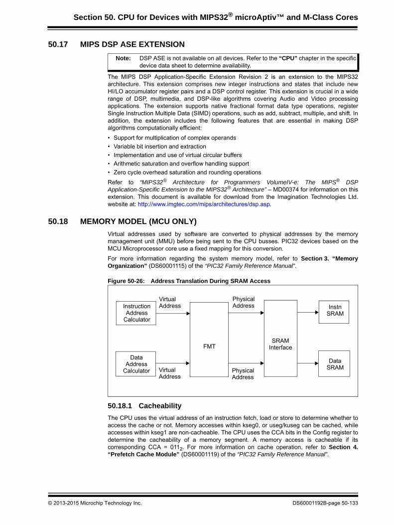
Section 50. CPU for Devices with MIPS32® microAptiv™ and M-Class Cores
50.17 MIPS DSP ASE EXTENSION
The MIPS DSP Application-Specific Extension Revision 2 is an extension to the MIPS32architecture. This extension comprises new integer instructions and states that include newHI/LO accumulator register pairs and a DSP control register. This extension is crucial in a widerange of DSP, multimedia, and DSP-like algorithms covering Audio and Video processingapplications. The extension supports native fractional format data type operations, registerSingle Instruction Multiple Data (SIMD) operations, such as add, subtract, multiple, and shift. Inaddition, the extension includes the following features that are essential in making DSPalgorithms computationally efficient:
• Support for multiplication of complex operands
• Variable bit insertion and extraction
• Implementation and use of virtual circular buffers
• Arithmetic saturation and overflow handling support
• Zero cycle overhead saturation and rounding operations
Refer to “MIPS32® Architecture for Programmers VolumeIV-e: The MIPS® DSPApplication-Specific Extension to the MIPS32® Architecture” – MD00374 for information on thisextension. This document is available for download from the Imagination Technologies Ltd.website at: http://www.imgtec.com/mips/architectures/dsp.asp.
50.18 MEMORY MODEL (MCU ONLY)
Virtual addresses used by software are converted to physical addresses by the memorymanagement unit (MMU) before being sent to the CPU busses. PIC32 devices based on theMCU Microprocessor core use a fixed mapping for this conversion.
For more information regarding the system memory model, refer to Section 3. “MemoryOrganization” (DS60001115) of the “PIC32 Family Reference Manual”.
Figure 50-26: Address Translation During SRAM Access
50.18.1 Cacheability
The CPU uses the virtual address of an instruction fetch, load or store to determine whether toaccess the cache or not. Memory accesses within kseg0, or useg/kuseg can be cached, whileaccesses within kseg1 are non-cacheable. The CPU uses the CCA bits in the Config register todetermine the cacheability of a memory segment. A memory access is cacheable if itscorresponding CCA = 0112. For more information on cache operation, refer to Section 4.“Prefetch Cache Module” (DS60001119) of the “PIC32 Family Reference Manual”.
Note: DSP ASE is not available on all devices. Refer to the “CPU” chapter in the specificdevice data sheet to determine availability.
SRAMInterface
InstnSRAM
DataSRAM
FMT
InstructionAddress
Calculator
DataAddress
Calculator
VirtualAddress
VirtualAddress
PhysicalAddress
PhysicalAddress
© 2013-2015 Microchip Technology Inc. DS60001192B-page 50-133

PIC32 Family Reference Manual
50.18.1.1 LITTLE ENDIAN BYTE ORDERING
On CPUs that address memory with byte resolution, there is a convention for multi-byte dataitems that specify the order of high-order to low-order bytes. Big-endian byte-ordering is wherethe lowest address has the MSB. Little-endian ordering is where the lowest address has the LSBof a multi-byte datum. The PIC32 CPU supports little-endian byte ordering.
Figure 50-27: Big-Endian Byte Ordering
Figure 50-28: Little-Endian Byte Ordering
HigherAddress Word
Address
LowerAddress
Bit #
} 1 word = 4 bytes
12
8
4
0
13
9
5
1
14
10
6
2
15
11
7
3
31 24 23 1615 8 7 012
8
4
0
HigherAddress Word
Address
LowerAddress
Bit #
15
11
7
3
14
10
6
2
13
9
5
1
12
8
4
0
31 24 23 1615 8 7 012
8
4
0
DS60001192B-page 50-134 © 2013-2015 Microchip Technology Inc.
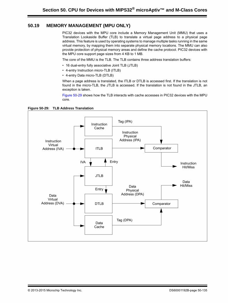
Section 50. CPU for Devices with MIPS32® microAptiv™ and M-Class Cores
50.19 MEMORY MANAGEMENT (MPU ONLY)
PIC32 devices with the MPU core include a Memory Management Unit (MMU) that uses aTranslation Lookaside Buffer (TLB) to translate a virtual page address to a physical pageaddress. This feature is used by operating systems to manage multiple tasks running in the samevirtual memory, by mapping them into separate physical memory locations. The MMU can alsoprovide protection of physical memory areas and define the cache protocol. PIC32 devices withthe MPU core support page sizes from 4 KB to 1 MB.
The core of the MMU is the TLB. The TLB contains three address translation buffers:
• 16 dual-entry fully associative Joint TLB (JTLB)
• 4-entry Instruction micro-TLB (ITLB)
• 4-entry Data micro-TLB (DTLB)
When a page address is translated, the ITLB or DTLB is accessed first. If the translation is notfound in the micro-TLB, the JTLB is accessed. If the translation is not found in the JTLB, anexception is taken.
Figure 50-29 shows how the TLB interacts with cache accesses in PIC32 devices with the MPUcore.
Figure 50-29: TLB Address Translation
InstructionCache
ITLB
JTLB
DTLB
DataCache
Tag (IPA)
InstructionPhysical
Address (IPA)
Comparator
IVA Entry
Entry
InstructionVirtual
Address (IVA)
DataVirtual
Address (DVA)
DataPhysical
Address (DPA)
Tag (DPA)
Comparator
InstructionHit/Miss
DataHit/Miss
© 2013-2015 Microchip Technology Inc. DS60001192B-page 50-135

PIC32 Family Reference Manual
50.19.1 Virtual Memory and Modes of Operation
All PIC32 devices support three modes of operation:
• User mode
• Kernel mode
• Debug mode
The core enters Kernel mode at reset, and when an exception is recognized. While in Kernelmode, the software has access to the entire 4 GB address space, as well as the CP0 registers.
User mode access is restricted to the first 2 GB of the address space (0x00000000 through0x7FFFFFFF), and can be excluded from accessing CP0 functions. Accessing a virtual addressabove 0x7FFFFFFF in User mode will cause an exception.
Debug mode is entered on a debug exception. While in Debug mode, the software has accessto all Kernel mode addresses and functions, as well as debug segment dseg, which overlays partof the kernel segment kseg3.
The virtual memory segments are different depending on the mode of operation. SeeFigure 50-14 in 50.11.4 “Processor Modes” for the PIC32 virtual memory map.
50.19.1.1 MAPPED AND UNMAPPED SEGMENTS
Memory segments that use the MMU to translate virtual page address into physical memorylocations are considered to be mapped. Those that do not use the MMU are consideredunmapped. Unmapped segments have a fixed translation from virtual to physical addresses. Atreset, it is important to execute from unmapped memory until the TLB is programmed to performaddress translation.
Except for kseg0, unmapped segments are always uncached. The cacheability of kseg0 is set inthe K0 field of the CP0 register. The cacheability of mapped segments is set in the K23 and KUfields of the CP0 register. Figure 50-30 shows the mapped and unmapped virtual memory areasfor Kernel mode and User mode. When operating in Debug mode, the dseg area is unmapped.The mapping for all other areas is the same as Kernel mode.
Figure 50-30: User and Kernel Mode Virtual Mapping
0xFFFFFFFF
0x800000000x7FFFFFFF
0x00000000
User Mode Kernel Mode
0xFFFFFFFF
0x800000000x7FFFFFFF
0x00000000
0xE00000000xDFFFFFFF
0xC00000000xBFFFFFFF
0xA00000000x7FFFFFFF
Reserved
2 GB Mapped
512 MB Mapped
512 MB Mapped
512 MB Unmapped
512 MB Unmapped
2 GB Mappeduseg kuseg
kseg3
kseg2
kseg1
kseg0
DS60001192B-page 50-136 © 2013-2015 Microchip Technology Inc.

Section 50. CPU for Devices with MIPS32® microAptiv™ and M-Class Cores
50.19.2 Translation Lookaside Buffer (TLB)
The TLB consists of one joint and two micro address translation buffers:
• 16 dual-entry fully associative Joint TLB (JTLB)
• 4-entry fully associative Instruction micro-TLB (ITLB)
• 4-entry fully associative Data micro-TLB (DTLB)
50.19.2.1 JOINT TLB
The JTLB maps 32 virtual page addresses to their corresponding physical addresses. Thepurpose of the TLB is to translate virtual page addresses along with their corresponding AddressSpace ID (ASID) into a physical memory address. Operating systems typically assign an ASIDto each user program or process. The TLB helps the operating system separate each userprocess into its own physical memory space.
The virtual to physical translation is performed by comparing the upper bits of the virtual addressand the ASID bits against each of the JTLB tag entries. The JTLB is referred to as a “Joint” TLBbecause it is used to translate both instruction and data virtual page addresses.
The JTLB is organized as pairs of even and odd entries containing address translations of pagesranging from 4 KB to 1 MB in size. Each virtual tag entry corresponds to two physical data entries,an even page entry and an odd page entry. The highest order virtual address bit not participatingin the tag comparison is used to determine which of the two data entries is used. Figure 50-31shows the contents of one the dual entries in the JTLB.
Figure 50-31: JTLB Entry (Tag and Data)
PageMask<28:11>
VPN2<31:13>
PFN0<31:12>
PFN1<31:12>
G ASID<7:0>
RI0
RI1
XI0
XI1
C0<2:0>
C1<2:0>
D0
D1
V0
V1
© 2013-2015 Microchip Technology Inc. DS60001192B-page 50-137

PIC32 Family Reference Manual
Table 50-41 describes each field of a JTLB entry.
Table 50-41: TLB Tag Entry Fields
A table entry is filled with a TLBWI or TLBWR instruction. Before executing either instruction, thefollowing CP0 registers must be updated with the information to be written to the TLB entry:
• PageMask is set in the PageMask register (CP0 Register 5, Select 0).• VPN2, VPN2X, and ASID are set in the EntryHi register (CP0 Register 10, Select 0)• PFN0, C0, D0, V0, and G are set in the EntryLo0 register (CP0 Register 2, Select 0)• PFN1, C1, D1, V1, and G are set in the EntryLo1 register (CP0 Register 3, Select 0)
Bit Name Description
PageMask<28:11> Page Mask Value. The Page Mask defines the page size by masking the appropriate VPN2 bits. It also determines which address bit is used to make the even-odd page (PFN0-PFN1) determination.
VPN2<31:13> Virtual Page Number divided by two. This field contains the upper bits of the virtual page number divided by two. Because it represents a pair of TLB pages, it is divided by two. Bits <31:25> are always included in the TLB lookup comparison. Bits <24:13> are included depending on the page size, defined by PageMask.
G Global Bit. When set, indicates that this entry is global to all address spaces, and therefore excludes the ASID in the TLB lookup comparison.
ASID<7:0> Address Space Identifier. Identifies which process or thread this TLB entry is associated with.
PFN0<31:12>PFN1<31:12>
Physical Frame Number. Defines the upper bits of the physical address. For page sizes larger than 4KB, only a subset of these bits is actually used.
C0<2:0>C1<2:0>
Cacheability. Indicates the cacheability attributes and determines whether the page should be placed in the cache or not.
RI0RI1
Read Inhibit bit. Indicates that the page is read protected. If this bit is set, and the IEC bit of the PageGrain register is set, any attempt to read from the page will result in a TLB Read Inhibit exception.
XI0XI1
Execute Inhibit bit. Indicates that the page is execution protected. If this bit is set, and the IEC bit of the PageGrain register is set, any attempt to fetch an instruction from the page will result in a TLB Execute Inhibit exception.
D0D1
Dirty bit. Indicates that the page has been written and/or is writable. If this bit is set, writes to the page are allowed. If this bit is not set, writes to the page will result in a TLB Modified exception.
V0V1
Valid bit. Indicates that the TLB entry is valid. If this bit is set, accesses to the page are permitted. If the bit is not set, accesses to the page will result in a TLB Invalid exception.
PageMask Page Size Even/Odd Bank Select Bit
00 0000 0000 0000 0011 4 KB VAddr<12>
00 0000 0000 0000 1111 16 KB VAddr<14>
00 0000 0000 0011 1111 64 KB VAddr<16>
00 0000 0000 1111 1111 256 KB VAddr<18>
00 0000 0011 1111 1111 1 MB VAddr<20>
C<2:0> Coherency Attribute
000 Cacheable, non-coherent, write-through, no write-allocate
001 Cacheable, non-coherent, write-through, write-allocate
010 Uncached
011 Cacheable, non-coherent, write-back, write-allocate
100-111 Reserved
Note: The global bit is part of the EntryLo0 and EntryLo1 registers. The value written tothe G bit in the JTLB is the logical AND of the G bits in the EntryLo0 and EntryLo1registers.
DS60001192B-page 50-138 © 2013-2015 Microchip Technology Inc.

Section 50. CPU for Devices with MIPS32® microAptiv™ and M-Class Cores
50.19.2.2 micro-TLBs (ITLB AND DTLB)
The ITLB is a small (i.e., micro) TLB dedicated to the instruction stream. The DTLB is a smallTLB that provides a faster translation for Load/Store addresses than is possible with the JTLB.Both are 4-entry, fully associative, and managed entirely by hardware.
Instruction fetch address translation is handled first by the ITLB. If the fetch misses the ITLB, theJTLB is accessed in the following clock cycle. If successful, the entry is copied into the ITLB. TheITLB is then accessed again, and the address is successfully translated.
Data translations access the ITLB and the JTLB in parallel. If there is a DTLB miss and a JTLBhit, the DTLB can be reloaded in the same clock cycle. The DTLB is then accessed on the nextclock cycle.
50.19.3 Virtual to Physical Address Translation
Essentially, the TLB acts a cache for page table entries. When a virtual address is converted toa physical address, the Virtual Page Number (VPN) of the address (the upper bits of the address)is compared with the virtual page numbers stored in the TLB. A TLB hit occurs when the followingconditions are met:
• The VPN of the virtual address matches a VPN stored in the TLB and:
- The Global (G) bit of both the even and odd pages of the TLB entry are set, or
- The ASID field of the virtual address is the same as the ASID field of the TLB entry
If these two conditions are not met, a TLB miss exception is taken by the processor and softwareis allowed to refill the TLB from a page table of virtual/physical addresses in memory.
Figure 50-32 shows the translation of a virtual address into a physical address.
Figure 50-32: Virtual to Physical Address Translation
Each JTLB entry contains a tag and two data fields. On a TLB hit, the upper bits of the virtualaddress are replaced with the Page Frame Number (PFN) stored in the corresponding data field.On a TLB miss, an exception is taken and software refills the TLB from a page table stored inmemory.
G ASID VPN
C0
C1
D0
D1
V0
V1
PFN0
PFN1
TLB Entry
TLB
G ASID VPN Offset
Virtual Address
Physical Address
PFN Offset
© 2013-2015 Microchip Technology Inc. DS60001192B-page 50-139

PIC32 Family Reference Manual
50.19.4 TLB Entry Replacement
On a normal TLB miss, JTLB entries are replaced by a random replacement algorithm. The CPUalso provides the ability to lock a programmable number of mappings into the TLB via the CP0Wired register (see Register 50-8 for details).
The JTLB supports pages of different sizes ranging from 4 KB to 1 MB in powers of four. Thepage size can be configured on a per-entry basis by loading the CP0 PageMask register with thedesired page size prior to writing a new entry. A common use for this feature is to map a largememory block (such as a frame buffer) with a single TLB entry.
50.19.5 TLB Instructions
Table 50-42 lists the TLB-related instructions supported by the PIC32. See 50.21.5.5 “TLBInstructions (MPU Only)” for details on these instructions.
Table 50-42: TLB Instructions
Instruction Description
TLBP Translation Lookaside Buffer Probe
TLBR Translation Lookaside Buffer Read
TLBWI Translation Lookaside Buffer Write Index
TLBWR Translation Lookaside Buffer Write Random
DS60001192B-page 50-140 © 2013-2015 Microchip Technology Inc.

Section 50. CPU for Devices with MIPS32® microAptiv™ and M-Class Cores
50.20 L1 CACHES (MPU ONLY)
PIC32 devices with the MPU microprocessor core have separate instruction and data caches.The use of separate caches allows instruction and data references to happen simultaneously.Both caches are Virtually Index, Physically-tagged (VIPT), allowing cache access to occur inparallel with virtual-to-physical address translation.
50.20.1 Cache Configuration
The instruction and data caches may have different sizes and associativities. For example, theinstruction cache may be 16 KB in size with 4-way set associativity, while the data cache may be4 KB with 2-way set associativity. A set-associative cache is a compromise betweendirect-mapped and fully-associative caches.
In a direct-mapped cache, any location in memory can only be mapped to a single location in thecache. A direct-mapped cache is simple to implement and address, but can be inflexible and leadto thrashing when two heavily used memory locations share the same mapping.
A fully-associative cache allows any location in memory to map to any location in cache. Thisminimizes collisions, but is expensive to implement.
In a set-associative cache, the cache is divided into groups of lines known as sets. The numberof lines per set is known as the associativity. Each memory location is mapped to a set, and maybe cached in any line within the set. For example, in a 16 KB, 16 bytes per line, 4-wayset-associative cache, the cache is divided into 256 sets of four lines each. As shown, inFigure 50-33, any cacheable (16-byte) memory location is mapped to a single set, and may bemapped to any of four lines within the set. In a system with 64 MB of cacheable memory, eachset is shared by 16,384 (256 x 16-bytes) blocks of memory.
Figure 50-33: MPU 16 Kbyte 4-way Set-Associative Cache
Memory
MemoryBlock 16,383
L1 Cache (16 KB) Physical Memory (64 MB)
Block 04 KB
(256 x 16 bytes)
MemoryBlock 1
4 KB(256 x 16 bytes)
Set 0(4 x 16 bytes)
Set 1(4 x 16 bytes)
0
255
4 KB(256 x 16 bytes)
1
256
511
257
4,194,048
4,194,303
4,194,049Set 255
(4 x 16 bytes)
(See Figure 50-34 fordetails.)
© 2013-2015 Microchip Technology Inc. DS60001192B-page 50-141

PIC32 Family Reference Manual
50.20.2 Cache Organization
Each cache line is organized into three arrays:
• Tag
• Data
• Way-select
The tag array holds the physical address of the cached memory location, and the data arrayholds the cached (16-byte) instruction or data. The tag and data arrays hold four lines ofinformation per set, corresponding to the 4-way set associativity of the cache. The way-selectarray holds Least Recently Used (LRU) bits that are decoded to select the way to be replaced,according to a LRU algorithm. In the data cache, this array also holds the dirty bits, which indicatewhether or not the data needs to be written back to memory before being replaced in the cache.
Figure 50-34: Cache Array Formats
Definitions for Figure 50-34 are as follows:
• Physical Address: The upper 22 bits of the physical address (bits <31:10>)
• Lock: This bit is set or cleared using the CACHE instruction. When set, the cache line is “locked” (i.e., it cannot be selected for replacement on a cache miss).
• Valid: Indicates whether or not the data in the cache line is valid
• Word 0-3: Instruction or data words from memory. Each cache line stores four 32-bit words.
• Dirty: Present only in the data cache array, there is one dirty bit for each way. The dirty bit is set when data in the cache line is modified. This lets the CPU know to write the cache line back to memory before it is replaced on a cache fill.
• LRU: These bits indicate the way to be replaced according to a Least Recently Used (LRU) algorithm
22 1 1
Physical Address Lock ValidWay 1
22 1 1
Physical Address Lock ValidWay 2
22 1 1
Physical Address Lock ValidWay 3
22 1 1
Physical Address Lock ValidWay 4
Word3 Word2 Word1 Word0
32 32 32 32
Word3 Word2 Word1 Word0
32 32 32 32
Word3 Word2 Word1 Word0
32 32 32 32
Word3 Word2 Word1 Word0
32 32 32 32
Dirty(1) LRU
4 6
Way-Select
Tag Data
Note 1: Data Cache only.
DS60001192B-page 50-142 © 2013-2015 Microchip Technology Inc.

Section 50. CPU for Devices with MIPS32® microAptiv™ and M-Class Cores
50.20.3 Cacheability Attributes
The cacheability attributes of kseg0 can be set with the CP0 Config1 register. The cacheabilityoptions are:
• Uncached: Addresses in an uncached memory area are read from main memory, and not from cache. Writes to uncached memory areas are written directly to main memory, without changing the cache contents.
• Write-back with write allocation: Loads and instruction fetches first search the cache, reading main memory only if the desired data does not reside in the cache. On data store operations, the cache is first searched to see if the target address is resident in the cache. If it is resident, the cache contents are updated, but main memory is not written. If the cache lookup misses on a store, main memory is read to bring the line into the cache and merge it with the new store data. Therefore, the allocation policy on a cache miss is read- or write-allocate. Data stores will update the appropriate dirty bit in the way-select array to indicate that the line contains modified data. When a line with dirty data is displaced from the cache, it is written back to memory.
• Write-through with no write allocation: Loads and instruction fetches first search the cache, reading main memory only if the desired data does not reside in the cache. On data store operations, the cache is first searched to see if the target address is resident in the cache. If it is resident, the cache contents are updated, and main memory is also written. If the cache lookup misses on a store, only main memory is written. Therefore, the allocation policy on a cache miss is read-allocate only.
• Write-through with write allocation: Loads and instruction fetches first search the cache, reading main memory only if the desired data does not reside in the cache. On data store operations, the cache is first searched to see if the target address is resident in the cache. If it is resident, the cache contents are updated, and main memory is also written. If the cache lookup misses on a store, main memory is read to bring the line into the cache and merge it with the new store data. In addition, the store data is also written to main memory. Therefore, the allocation policy on a cache miss is read- or write-allocate.
50.20.4 Cache Replacement Policy
The cache replacement policy refers to how the cache determines which way within a set to fillon a cache miss. In a normal cache miss, the lock and LRU tag bits are used to determine theway that is filled. If all ways are valid, any locked ways will not be replaced. If all ways are locked,fill data will not fill into the cache, and Write-back stores turn into Write-through, Write-allocatestores. If the way being replaced is dirty, the 16-byte line will be written back to memory beforethe fill takes place.
The LRU field in the way-select array is updated in the following ways:
• On a cache hit, the associated way is updated to be the most recently used
• On a cache fill, the filled way is updated to be the most recently used
• On a CACHE instruction, the update of the LRU bits depends on the operation:
- Index (Writeback) Invalidate: Least recently used
- Index Load Tag: No update
- Index Store Tag (CP0 ErrCtl<WST> = 0): Most recently used if CP0 TagLo<V> = 1 Least recently used if CP0 TagLo<V> = 0
- Index Store Tag (CP0 ErrCtl<WST> = 1): Updated with contents of CP0 TagLo<LRU>
- Index Store Data: No update
- Hit Invalidate: Least recently used if a hit is generated; otherwise, no update
- Fill: Most recently used
- Hit Writeback: No update
- Fetch and Lock: Most recently used
© 2013-2015 Microchip Technology Inc. DS60001192B-page 50-143

PIC32 Family Reference Manual
50.20.5 Cache Instruction
The contents of the tag, data and way-select arrays can be manipulated by the user with theCACHE instruction. The user may fill, lock and invalidate individual cache lines by setting orclearing bits in the tag and data arrays. See 50.21.7 “MPU Cache Instruction” for details onhow to use the CACHE instruction.
50.20.6 Cache Coherency
Because a cache holds a copy of memory-resident data, it is possible for another bus master tomodify cached memory locations, rendering the cached data stale. Likewise, the CPU mayupdate the cache contents, rendering the corresponding memory data stale until it is writtenback. The PIC32 CPU has no hardware support for maintaining coherency between cache andmemory, so it must be handled by software. Most operating systems manage cache coherencyissues automatically. Programs running without the benefit of a operating system must managecache coherency internally.
In Write-through mode, all data writes are written to main memory. In Write-back mode, datawrites only go to the cache; the cache may contain the only valid copy of the data until it is writtento main memory by a line refill or a CACHE instruction.
50.20.7 Cache Initialization
The PIC32 L1 cache tag and data arrays power up to an unknown state and are not affected byreset. Therefore, the caches must be initialized before use. This is typically done by the bootcode by writing all-zero values to the tag array. Note that the boot code runs from uncachedmemory (kseg1).
DS60001192B-page 50-144 © 2013-2015 Microchip Technology Inc.

Section 50. CPU for Devices with MIPS32® microAptiv™ and M-Class Cores
50.21 CPU INSTRUCTIONS
CPU instructions are organized into the following functional groups:
• Load and store
• Computational
• Jump and branch
• Miscellaneous
• Coprocessor
Each instruction is 32 bits long.
50.21.1 CPU Load and Store Instructions
MIPS processors use a load/store architecture; all operations are performed on operands heldin processor registers and main memory is accessed only through load and store instructions.
50.21.1.1 TYPES OF LOADS AND STORES
There are several different types of load and store instructions, each designed for a differentpurpose:
• Transferring variously-sized fields (for example, LB, SW)
• Trading transferred data as signed or unsigned integers (for example, LHU)
• Accessing unaligned fields (for example, LWR, SWL)
• Atomic memory update (read-modify-write: for instance, LL/SC)
50.21.1.2 LIST OF CPU LOAD AND STORE INSTRUCTIONS
The following data sizes (as defined in the AccessLength field) are transferred by CPU load andstore instructions:
• Byte
• Half-word
• Word
Signed and unsigned integers of different sizes are supported by loads that either sign-extend orzero-extend the data loaded into the register.
Unaligned words and double words can be loaded or stored in just two instructions by using apair of special instructions. For loads a LWL instruction is paired with a LWR instruction. The loadinstructions read the left-side or right-side bytes (left or right side of register) from an aligned wordand merge them into the correct bytes of the destination register.
50.21.1.3 LOADS AND STORES USED FOR ATOMIC UPDATES
The paired instructions, Load Linked and Store Conditional, can be used to perform an atomicread-modify-write of word or double word cached memory locations. These instructions are usedin carefully coded sequences to provide one of several synchronization primitives, includingtest-and-set, bit-level locks, semaphores, and sequencers and event counts.
50.21.1.4 COPROCESSOR LOADS AND STORES
If a particular coprocessor is not enabled, loads and stores to that processor cannot execute andthe attempted load or store causes a Coprocessor Unusable exception. Enabling a coprocessoris a privileged operation provided by the System Control Coprocessor, CP0.
© 2013-2015 Microchip Technology Inc. DS60001192B-page 50-145

PIC32 Family Reference Manual
50.21.2 Computational Instructions
Two’s complement arithmetic is performed on integers represented in 2’s complement notation.These are signed versions of the following operations:
• Add
• Subtract
• Multiply
• Divide
The add and subtract operations labelled “unsigned” are actually modulo arithmetic withoutoverflow detection.
There are also unsigned versions of multiply and divide, as well as a full complement of shift andlogical operations. Logical operations are not sensitive to the width of the register.
MIPS32 provides 32-bit integers and 32-bit arithmetic.
50.21.2.1 SHIFT INSTRUCTIONS
The ISA defines two types of shift instructions:
• Those that take a fixed shift amount from a 5-bit field in the instruction word (for instance, SLL, SRL)
• Those that take a shift amount from the low-order bits of a general register (for instance, SRAV, SRLV)
50.21.2.2 MULTIPLY AND DIVIDE INSTRUCTIONS
The multiply instruction performs 32-bit by 32-bit multiplication and creates either 64-bit or 32-bitresults. Divide instructions divide a 64-bit value by a 32-bit value and create 32-bit results. Withone exception, they deliver their results into the HI and LO special registers. The MUL instructiondelivers the lower half of the result directly to a GPR.
• Multiply produces a full-width product twice the width of the input operands; the low half is loaded into LO and the high half is loaded into HI
• Multiply-Add and Multiply-Subtract produce a full-width product twice the width of the input operations and adds or subtracts the product from the concatenated value of HI and LO. The low half of the addition is loaded into LO and the high half is loaded into HI.
• Divide produces a quotient that is loaded into LO and a remainder that is loaded into HI
The results are accessed by instructions that transfer data between HI/LO and the generalregisters.
50.21.3 Jump and Branch Instructions
50.21.3.1 TYPES OF JUMP AND BRANCH INSTRUCTIONS DEFINED BY THE ISA
The architecture defines the following jump and branch instructions:
• PC-relative conditional branch
• PC-region unconditional jump
• Absolute (register) unconditional jump
• A set of procedure calls that record a return link address in a general register
50.21.3.2 BRANCH DELAYS AND THE BRANCH DELAY SLOT
All branches have an architectural delay of one instruction. The instruction immediately followinga branch is said to be in the “branch delay slot”. If a branch or jump instruction is placed in thebranch delay slot, the operation of both instructions is undefined.
By convention, if an exception or interrupt prevents the completion of an instruction in the branchdelay slot, the instruction stream is continued by re-executing the branch instruction. To permitthis, branches must be restartable; procedure calls may not use the register in which the returnlink is stored (usually GPR 31) to determine the branch target address.
DS60001192B-page 50-146 © 2013-2015 Microchip Technology Inc.

Section 50. CPU for Devices with MIPS32® microAptiv™ and M-Class Cores
50.21.3.3 BRANCH AND BRANCH LIKELY
There are two versions of conditional branches; they differ in the manner in which they handlethe instruction in the delay slot when the branch is not taken and execution falls through.
• Branch instructions execute the instruction in the delay slot
• Branch likely instructions do not execute the instruction in the delay slot if the branch is not taken (they are said to nullify the instruction in the delay slot)
50.21.4 microMIPS Instructions
The microMIPS ISA introduces several new instructions, including the ability to load or storemultiple 16-bit or 32-bit words from/to memory. Refer to the “MIPS® Architecture forProgrammers Volume II-B: The microMIPS32™ Instruction Set” - MD00582, for the full listingand complete description of the microMIPS ISA. This document is available from the ImaginationTechnologies Ltd. website at: http://www.imgtec.com/mips/architectures/mips32.asp.
50.21.5 Miscellaneous Instructions
50.21.5.1 INSTRUCTION SERIALIZATION (SYNC AND SYNCI)
In normal operation, the order in which load and store memory accesses appear to a viewer out-side the executing processor (for instance, in a multiprocessor system) is not specified by thearchitecture.
The SYNC instruction can be used to create a point in the executing instruction stream at whichthe relative order of some loads and stores can be determined: loads and stores executed beforethe SYNC are completed before loads and stores after the SYNC can start.
The SYNCI instruction synchronizes the processor caches with previous writes or other modifications to the instruction stream.
50.21.5.2 EXCEPTION INSTRUCTIONS
Exception instructions transfer control to a software exception handler in the kernel. There aretwo types of exceptions, conditional and unconditional. These are caused by the followinginstructions: syscall, trap, and break.
Trap instructions cause conditional exceptions based upon the result of a comparison. Systemcall and breakpoint instructions cause unconditional exceptions.
50.21.5.3 CONDITIONAL MOVE INSTRUCTIONS
MIPS32 includes instructions to conditionally move one CPU general register to another, basedon the value in a third general register.
50.21.5.4 NOP INSTRUCTIONS
The NOP instruction is actually encoded as an all-zero instruction. MIPS processors special-casethis encoding as performing no operation, and optimize execution of the instruction. In addition,the SSNOP instruction takes up one issue cycle on any processor, including super-scalarimplementations of the architecture.
50.21.5.5 TLB INSTRUCTIONS (MPU ONLY)
The TLBR, TLBWI and TLBWR instructions can be used to read or write TLB entries. The Indexregister is loaded with the VPN of a TLB entry, and the tag contents are read into the EntryLo0,EntryLo1 and PageMask registers. TLB entries are written in a similar manner using the TLBWIand TLBWR instructions.
Note: Although the Branch Likely instructions are included in this specification, softwareis strongly encouraged to avoid the use of the Branch Likely instructions, as theywill be removed from a future revision of the MIPS architecture.
© 2013-2015 Microchip Technology Inc. DS60001192B-page 50-147

PIC32 Family Reference Manual
50.21.6 Coprocessor Instructions
50.21.6.1 WHAT COPROCESSORS DO
Coprocessors are alternate execution units, with register files separate from the CPU. In abstrac-tion, the MIPS architecture provides for up to four coprocessor units, numbered 0 to 3. Each levelof the ISA defines a number of these coprocessors. Coprocessor 0 is always used for systemcontrol and coprocessor 1 and 3 are used for the floating point unit. Coprocessor 2 is reservedfor implementation-specific use. PIC32 devices only implement Coprocessor 0.
A coprocessor may have two different register sets:
• Coprocessor general registers
• Coprocessor control registers
Each set contains up to 32 registers. Coprocessor computational instructions may use theregisters in either set.
50.21.6.2 SYSTEM CONTROL COPROCESSOR 0 (CP0)
The system controller for all MIPS processors is implemented as coprocessor 0 (CP0), theSystem Control Coprocessor. It provides the processor control, memory management, andexception handling functions.
50.21.6.3 COPROCESSOR LOAD AND STORE INSTRUCTIONS
Explicit load and store instructions are not defined for CP0; the move to and from coprocessorinstructions must be used to write and read the CP0 registers.
50.21.7 MPU Cache Instruction
The CACHE instruction can be used to read or write the data, tag or way-select arrays. It takestwo arguments: a 5-bit operation field, and a 16-bit offset field. The format is similar to a load andstore instruction, with the offset field consisting of a base register plus 16-bit signed immediateoffset:
cache OP, offset(base)
The 16-bit offset is sign-extended and added to the contents of the base register to form an effectiveaddress. The effective address can be one of two types:
• Address: The effective address is the virtual memory location of some instruction or data, and is processed just like a normal cached access.
• Index: The effective address encodes the cache virtual index, the byte location within the cache line, and the way. The exact size and boundary of each value depends on the cache size and configuration. In general, an index effective address has the following format, as shown in Figure 50-35.
Figure 50-35: Cache Effective Address
Where:
b_offset = 4
b_index = log2 (cache_size associativity)
b_way = b_index + 2
For a 32 KB, 4-way associative cache:
b_index = log2(32768 4) = 13
b_way = 15
Reserved Way Index Byte Index
b_way b_index b_offset
DS60001192B-page 50-148 © 2013-2015 Microchip Technology Inc.

Section 50. CPU for Devices with MIPS32® microAptiv™ and M-Class Cores
The operation field encodes the cache on which to perform the operation and the operation itself,as shown in Figure 50-36.
Figure 50-36: Cache Operation
The lower two bits of the operation field specify the cache on which to perform the operation, asshown in Table 50-43.
Table 50-43: Cache Instruction OP bits Encoding (Cache)
The remaining bits of the operation field specify the operation to perform, as shown inTable 50-44.
Table 50-44: Cache Instruction OP bits Encoding
OP<1:0> bits Cache
‘0b00 Instruction Cache
‘0b01 Data Cache
‘0b10 Reserved
‘0b11 Reserved
CacheOperation
b2 b0
OP<4:2> bits Cache Name Type Operation
‘0b000
Instruction
Index Invalidate Index
Set the state of the cache block at the specified address to invalid. Commonly used to initialize the instruction cache at startup.
Data
Set the state of the cache block at the specified address to invalid. If invalid and dirty, write back to memory first. Should NOT be used to initialize the data cache at startup.
‘0b001 — — — Reserved.
‘0b010 Both Index Store Tag IndexSets the cache tag using the values from the TagLo register. Commonly used to initialize the data cache at startup by setting TagLo to zero.
‘0b011 — — — Reserved.
‘0b100 Both Hit Invalidate AddressIf the cache block contains the specified address, set to invalid. Do not write back if dirty.
‘0b101
Instruction
Fill Address
Fill the cache from the specified address. Similar to a cache miss.
DataIf the cache block contains the specified address, set to invalid. Write back if dirty. Recommended way to invalidate a cache line in a running cache.
‘0b110 — — — Reserved.
‘0b111 — — — Reserved.
© 2013-2015 Microchip Technology Inc. DS60001192B-page 50-149

PIC32 Family Reference Manual
The CACHE Index Load Tag and Index Store Tag instructions can be used to read and write theLRU bits in the instruction or data cache way-select arrays by setting the WST bit in the ErrCtlCP0 register. Valid LRU field values are shown in Table 50-45.
Table 50-45: LRU bit Way Selection Encoding
The order is indicated by listing the least-recently used way to the left and the most-recently usedway to the right. Note that not all values are valid.
Selection Order
LRU<5:0> bits
Selection Order
LRU<5:0> bits
Selection Order
LRU<5:0> bits
Selection Order
LRU<5:0> bits
0123 000000 1023 000100 2013 100010 3012 011001
0132 000001 1032 000101 2031 110010 3021 011011
0213 000010 1203 100100 2103 100110 3102 011101
0231 010010 1230 101100 2130 101110 3120 111101
0312 010001 1302 001101 2301 111010 3201 111011
0321 010011 1320 101101 2310 111110 3210 111111
DS60001192B-page 50-150 © 2013-2015 Microchip Technology Inc.

Section 50. CPU for Devices with MIPS32® microAptiv™ and M-Class Cores
50.22 MIPS DSP ASE INSTRUCTIONS
The MIPS DSP ASE Revision 2 instructions can be classified into the following subclasses:
• Arithmetic• GPR-based shift• Multiply• Bit manipulation• Compare-Pick• DSP Control Access• Indexed-Load• Branch
The MIPS DSP ASE adds four new registers. The software is required to recognize the presenceof the MIPS DSP ASE and to include these additional registers in context save and restore oper-ations.
Three additional HI/LO registers are available to create a total of four accumulator registers.Many common DSP computations involve accumulation (e.g., convolution). MIPS DSP ASERevision 2 instructions that target the accumulators use two bits to specify the destination accu-mulator, with the zero value referring to the original accumulator of the MIPS architecture.
A new control register, DSPControl, is used to hold extra state bits needed for efficient supportof the new instructions. Register 50-63 illustrates the bits in this register.
50.22.1 DSPControl Register
The DSPControl register is used to hold extra state bits needed for efficient support of the MIPSDSP ASE Revision 2 instruction set.
Note: DSP ASE is not available on all devices. Refer to the “CPU” chapter in the specificdevice data sheet to determine availability.
Note: This register is not available on all devices. Refer to the “CPU” chapter in thespecific device data sheet to determine availability.
Register 50-63: DSPControl: MIPS DSP ASE Control Register
Bit Range
Bit31/23/15/7
Bit30/22/14/6
Bit29/21/13/5
Bit28/20/12/4
Bit27/19/11/3
Bit26/18/10/2
Bit25/17/9/1
Bit24/16/8/0
31:24U-0 U-0 U-0 U-0 R/W-0 R/W-0 R/W-0 R/W-0
— — — — CCOND<3:0>
23:16R/W-0 R/W-0 R/W-0 R/W-0 R/W-0 R/W-0 R/W-0 R/W-0
OUFLAG<7:0>
15:8U-0 R/W-0 R/W-0 R/W-0 R/W-0 R/W-0 R/W-0 R/W-0
— EFI C SCOUNT<5:1>
7:0R/W-0 U-0 R/W-0 R/W-0 R/W-0 R/W-0 R/W-0 R/W-0
SCOUNT<0> — POS<5:0>
Legend:
R = Readable bit W = Writable bit U = Unimplemented bit, read as ‘0’
-n = Value at POR ‘1’ = Bit is set ‘0’ = Bit is cleared x = Bit is unknown
bit 31-28 Unimplemented: Read as ‘0’
bit 27-24 CCOND<3:0>: Condition Code bits
These bits are set by vector comparison instructions and are used as source selectors by the group of PICK instructions. The vector element size determines the number of bits set by a comparison (1, 2, or 4). Bits that are not set after the comparison are unpredictable.
© 2013-2015 Microchip Technology Inc. DS60001192B-page 50-151

PIC32 Family Reference Manual
bit 23-16 OUFLAG<7:0>: Overflow/Underflow Indication bits
The bits of the overflow flag OUFLAG<7:0> are set by the instructions listed in the following table. These bits are sticky and can be reset only by an explicit write to these bits in the register (using the WRDSP instruction).
bit 15 Unimplemented: Read as ‘0’
bit 14 EFI: Extract Fail Indicator bit
This bit is set to ‘1’ when one of the extraction instructions (EXTP, EXTPV, EXTPDP, or EXTPDPV) fails. A failure occurs when there are insufficient bits to extract (i.e., when the value of the POS<5:0> bits is less than the size argument specified in the instruction.
bit 13 C: Carry bit
This bit is set and used by a special add instruction to implement a 64-bit addition across two GPRs in a microMIPS32 implementation. Instruction ADDSC sets the bit and instruction ADDWC uses this bit.
bit 12-7 SCOUNT<5:0>: Size Count bit
This bit is used by the INSV instruction to specify the size of the bit field to be inserted.
bit 6 Unimplemented: Read as ‘0’
bit 5-0 POS<5:0>: Insert/Extract Position bits
These bits are used by the variable insert instruction, INSV, to specify the position to insert bits. It is also used to indicate the extract position for the EXTP, EXTPV, EXTPDP, or EXTPDPV instructions.
Register 50-63: DSPControl: MIPS DSP ASE Control Register (Continued)
Bit Number Description
23 This bit is set when the destination is accumulator (HI-LO pair) zero, and an operation overflow or underflow occurs. These instructions are: DPAQ_S, DPAQ_SA, DPSQ_S, DPSQ_SA, DPAQX_S, DPAQX_SA, DPSQX_S, DPSQX_SA, MAQ_S, MAQ_SA and MULSAQ_S.
23 Same instructions as above, when the destination is accumulator (HI-LO pair) one.
21 Same instructions as above, when the destination is accumulator (HI-LO pair) two.
20 Same instructions as above, when the destination is accumulator (HI-LO pair) three.
19 Instructions that set this bit on an overflow/underflow: ABSQ_S, ADDQ, ADDQ_S, ADDU, ADDU_S, ADDWC, SUBQ, SUBQ_S, SUBU and SUBU_S.
18 Instructions that set this bit on an overflow/underflow: MUL, MUL_S, MULEQ_S, MULEU_S, MULQ_RS, and MULQ_S.
17 Instructions that set this bit on an overflow/underflow: PRECRQ_RS, SHLL, SHLL_S, SHLLV, and SHLLV_S.
16 Instructions that set this bit on an overflow/underflow: EXTR, EXTR_S, EXTR_RS, EXTRV, and EXTRV_RS.
DS60001192B-page 50-152 © 2013-2015 Microchip Technology Inc.

Section 50. CPU for Devices with MIPS32® microAptiv™ and M-Class Cores
50.23 CPU INITIALIZATION
Software is required to initialize the following parts of the device after a Reset event.
50.23.1 General Purpose Registers
The CPU register file powers up in an unknown state with the exception of r0 which is always ‘0’.Initializing the rest of the register file is not required for proper operation in hardware. However,depending on the software environment, several registers may need to be initialized. Some ofthese are:
• sp – Stack pointer
• gp – Global pointer
• fp – Frame pointer
50.23.2 Coprocessor 0 State
Miscellaneous CP0 states need to be initialized prior to leaving the boot code. There are variousexceptions that are blocked by ERL = 1 or EXL = 1, and which are not cleared by Reset. Thesecan be cleared to avoid taking spurious exceptions when leaving the boot code.
Table 50-46: CPU Initialization
50.23.3 System Bus
The System Bus should be initialized before switching to User mode or before executing fromDRM. The values written to the System Bus are based on the memory layout of the applicationto be run.
50.23.4 Caches (MPU Only)
The cache tag and data arrays power-up to an unknown state and are not affected by a reset.Every tag in the cache arrays should be initialized to an invalid state using the CACHE instruction(Index Invalidate function).
CP0 Register Action
Cause WP (Watch Pending), SW0/1 (Software Interrupts) should be cleared.
Config Typically, the K0, KU and K23 fields should be set to the desired Cache Coherency Algorithm (CCA) value prior to accessing the corresponding memory regions.
Count(1) Should be set to a known value if Timer Interrupts are used.
Compare(1) Should be set to a known value if Timer Interrupts are used. The write to Compare will also clear any pending Timer Interrupts (Thus, Count should be set before Compare to avoid any unexpected interrupts).
Status Desired state of the device should be set.
Other CP0 state Other registers should be written before they are read. Some registers are not explicitly writable, and are only updated as a by-product of instruction execution or a taken exception. Uninitialized bits should be masked off after reading these registers.
Note 1: When the Count register is equal to the Compare register a timer interrupt is signaled. There is a mask bit in the interrupt controller to disable passing this interrupt to the CPU if desired.
© 2013-2015 Microchip Technology Inc. DS60001192B-page 50-153

PIC32 Family Reference Manual
50.24 EFFECTS OF A RESET
50.24.1 Master Clear Reset
The PIC32 core is not fully initialized by a hardware Reset. Only a minimal subset of theprocessor state is cleared. This is enough to bring the core up while running in unmapped anduncached code space. All other processor state can then be initialized by software. Power-upReset brings the device into a known state. A Soft Reset can be forced by asserting the MasterClear (MCLR) pin. This distinction is made for compatibility with other MIPS processors. Inpractice, both resets are handled identically.
50.24.1.1 COPROCESSOR 0 STATE
Much of the hardware initialization occurs in Coprocessor 0, which are described in Table 50-47.
Table 50-47: Bits Cleared or Set by Reset
50.24.1.2 BUS STATE MACHINES
All pending bus transactions are aborted and the state machines in the SRAM interface unit arereset when a Reset or Soft Reset exception is taken.
50.24.2 Fetch Address
Upon Reset/Soft Reset, unless the EJTAGBOOT option is used, the fetch is directed to VA 0xB-FC00000 (PA 0x1FC00000). This address is in kseg1, which is unmapped and uncached.
50.24.3 WDT Reset
The status of the CPU registers after a WDT event depends on the operational mode of the CPUprior to the WDT event.
If the device was not in Sleep a WDT event will force registers to a Reset value.
Register Name Bit NameClearedor Set
Value Cleared or Set By
Status BEV Set 1 Reset or Soft Reset
TS Cleared 0 Reset or Soft Reset
SR Set 1 Soft Reset
SR Cleared 0 Reset
NMI Cleared 0 Reset or Soft Reset
ERL Set 1 Reset or Soft Reset
RP Cleared 0 Reset or Soft Reset
All Configuration Registers:ConfigConfig1Config2Config3Config4Config5Config7
Note: The reset state of the CP0 Configuration registers may varybetween devices. Refer to the “CPU” chapter in the specificdevice data sheet for details.
Debug DM Cleared 0 Reset or Soft Reset(1)
LSNM Cleared 0 Reset or Soft Reset
IBUSEP Cleared 0 Reset or Soft Reset
IEXI Cleared 0 Reset or Soft Reset
SSt Cleared 0 Reset or Soft Reset
Note 1: Unless EJTAGBOOT option is used to boot into Debug mode.
DS60001192B-page 50-154 © 2013-2015 Microchip Technology Inc.

Section 50. CPU for Devices with MIPS32® microAptiv™ and M-Class Cores
50.25 RELATED APPLICATION NOTES
This section lists application notes that are related to this section of the manual. Theseapplication notes may not be written specifically for the PIC32 device family, but the concepts arepertinent and could be used with modification and possible limitations. The current applicationnotes related to the PIC32 CPU for Devices with MIPS32® microAptiv™ and M-Class Coresinclude the following:
Title Application Note #
No related application notes at this time. N/A
Note: Please visit the Microchip Web site (www.microchip.com) for additional applicationnotes and code examples for the PIC32 family of devices.
© 2013-2015 Microchip Technology Inc. DS60001192B-page 50-155

PIC32 Family Reference Manual
50.26 REVISION HISTORY
Revision A (April 2013)
This is the initial released version of the document.
Revision B (July 2015)
This revision includes the following updates:
• The document title was changed to: “CPU for Devices with MIPS32® microAptiv™ and M-Class Cores”
• M-Class core related updates were implemented throughout the document
• All references to MIPS Technologies were changed to Imagination Technologies Ltd.
• The Select number for the Debug2 register was changed from 5 to 6 (see Register 50-45)
• The following registers were added:
- BadInstr: Bad Instruction Word Register; CP0 Register 8, Select 1 (Register 50-11)
- BadInstrP: Bad Prior Branch Instruction Register; CP0 Register 8, Select 2 (Register 50-12)
- CacheErr: Cache Error Register; CP0 Register 27, Select 0 (Register 50-51)
- KScratchn: Kernel Mode Scratchpad Registers; CP0 Register 31, Select 2-3 (Register 50-57)
• 50.5.2 “Architecture Release 5” was added
• 50.12 “Floating Point Unit (FPU)” was added
• 50.14 “Coprocessor 1 (CP1) Registers” was added, which includes the following registers:
- FIR: Floating Point Implementation Register; CP1 Control Register 0 (Register 50-58)
- FCC: Floating Point Condition Codes Register; CP1 Control Register 25 (Register 50-59)
- FEXR: Floating Point Exceptions Register; CP1 Control Register 26 (Register 50-60)
- FENR: Floating Point Enables Register; CP1 Control Register 28 (Register 50-61)
- FCSR: Floating Point Control and Status Register; CP1 Control Register 31 (Register 50-62)
• In addition, minor updates to text and formatting were incorporated throughout the document
DS60001192B-page 50-156 © 2013-2015 Microchip Technology Inc.

Note the following details of the code protection feature on Microchip devices:
• Microchip products meet the specification contained in their particular Microchip Data Sheet.
• Microchip believes that its family of products is one of the most secure families of its kind on the market today, when used in the intended manner and under normal conditions.
• There are dishonest and possibly illegal methods used to breach the code protection feature. All of these methods, to our knowledge, require using the Microchip products in a manner outside the operating specifications contained in Microchip’s Data Sheets. Most likely, the person doing so is engaged in theft of intellectual property.
• Microchip is willing to work with the customer who is concerned about the integrity of their code.
• Neither Microchip nor any other semiconductor manufacturer can guarantee the security of their code. Code protection does not mean that we are guaranteeing the product as “unbreakable.”
Code protection is constantly evolving. We at Microchip are committed to continuously improving the code protection features of ourproducts. Attempts to break Microchip’s code protection feature may be a violation of the Digital Millennium Copyright Act. If such actsallow unauthorized access to your software or other copyrighted work, you may have a right to sue for relief under that Act.
Information contained in this publication regarding deviceapplications and the like is provided only for your convenienceand may be superseded by updates. It is your responsibility toensure that your application meets with your specifications.MICROCHIP MAKES NO REPRESENTATIONS ORWARRANTIES OF ANY KIND WHETHER EXPRESS ORIMPLIED, WRITTEN OR ORAL, STATUTORY OROTHERWISE, RELATED TO THE INFORMATION,INCLUDING BUT NOT LIMITED TO ITS CONDITION,QUALITY, PERFORMANCE, MERCHANTABILITY ORFITNESS FOR PURPOSE. Microchip disclaims all liabilityarising from this information and its use. Use of Microchipdevices in life support and/or safety applications is entirely atthe buyer’s risk, and the buyer agrees to defend, indemnify andhold harmless Microchip from any and all damages, claims,suits, or expenses resulting from such use. No licenses areconveyed, implicitly or otherwise, under any Microchipintellectual property rights unless otherwise stated.
2013-2015 Microchip Technology Inc.
QUALITY MANAGEMENT SYSTEM CERTIFIED BY DNV
== ISO/TS 16949 ==
Trademarks
The Microchip name and logo, the Microchip logo, dsPIC, FlashFlex, flexPWR, JukeBlox, KEELOQ, KEELOQ logo, Kleer, LANCheck, MediaLB, MOST, MOST logo, MPLAB, OptoLyzer, PIC, PICSTART, PIC32 logo, RightTouch, SpyNIC, SST, SST Logo, SuperFlash and UNI/O are registered trademarks of Microchip Technology Incorporated in the U.S.A. and other countries.
The Embedded Control Solutions Company and mTouch are registered trademarks of Microchip Technology Incorporated in the U.S.A.
Analog-for-the-Digital Age, BodyCom, chipKIT, chipKIT logo, CodeGuard, dsPICDEM, dsPICDEM.net, ECAN, In-Circuit Serial Programming, ICSP, Inter-Chip Connectivity, KleerNet, KleerNet logo, MiWi, MPASM, MPF, MPLAB Certified logo, MPLIB, MPLINK, MultiTRAK, NetDetach, Omniscient Code Generation, PICDEM, PICDEM.net, PICkit, PICtail, RightTouch logo, REAL ICE, SQI, Serial Quad I/O, Total Endurance, TSHARC, USBCheck, VariSense, ViewSpan, WiperLock, Wireless DNA, and ZENA are trademarks of Microchip Technology Incorporated in the U.S.A. and other countries.
SQTP is a service mark of Microchip Technology Incorporated in the U.S.A.
Silicon Storage Technology is a registered trademark of Microchip Technology Inc. in other countries.
GestIC is a registered trademark of Microchip Technology Germany II GmbH & Co. KG, a subsidiary of Microchip Technology Inc., in other countries.
All other trademarks mentioned herein are property of their respective companies.
© 2013-2015, Microchip Technology Incorporated, Printed in the U.S.A., All Rights Reserved.
ISBN: 978-1-63277-631-0
DS60001192B-page 50-157
Microchip received ISO/TS-16949:2009 certification for its worldwide headquarters, design and wafer fabrication facilities in Chandler and Tempe, Arizona; Gresham, Oregon and design centers in California and India. The Company’s quality system processes and procedures are for its PIC® MCUs and dsPIC® DSCs, KEELOQ® code hopping devices, Serial EEPROMs, microperipherals, nonvolatile memory and analog products. In addition, Microchip’s quality system for the design and manufacture of development systems is ISO 9001:2000 certified.

60001192B-page 50-158 2013-2015 Microchip Technology Inc.
AMERICASCorporate Office2355 West Chandler Blvd.Chandler, AZ 85224-6199Tel: 480-792-7200 Fax: 480-792-7277Technical Support: http://www.microchip.com/supportWeb Address: www.microchip.com
AtlantaDuluth, GA Tel: 678-957-9614 Fax: 678-957-1455
Austin, TXTel: 512-257-3370
BostonWestborough, MA Tel: 774-760-0087 Fax: 774-760-0088
ChicagoItasca, IL Tel: 630-285-0071 Fax: 630-285-0075
ClevelandIndependence, OH Tel: 216-447-0464 Fax: 216-447-0643
DallasAddison, TX Tel: 972-818-7423 Fax: 972-818-2924
DetroitNovi, MI Tel: 248-848-4000
Houston, TX Tel: 281-894-5983
IndianapolisNoblesville, IN Tel: 317-773-8323Fax: 317-773-5453
Los AngelesMission Viejo, CA Tel: 949-462-9523 Fax: 949-462-9608
New York, NY Tel: 631-435-6000
San Jose, CA Tel: 408-735-9110
Canada - TorontoTel: 905-673-0699 Fax: 905-673-6509
ASIA/PACIFICAsia Pacific OfficeSuites 3707-14, 37th FloorTower 6, The GatewayHarbour City, Kowloon
Hong KongTel: 852-2943-5100Fax: 852-2401-3431
Australia - SydneyTel: 61-2-9868-6733Fax: 61-2-9868-6755
China - BeijingTel: 86-10-8569-7000 Fax: 86-10-8528-2104
China - ChengduTel: 86-28-8665-5511Fax: 86-28-8665-7889
China - ChongqingTel: 86-23-8980-9588Fax: 86-23-8980-9500
China - DongguanTel: 86-769-8702-9880
China - HangzhouTel: 86-571-8792-8115 Fax: 86-571-8792-8116
China - Hong Kong SARTel: 852-2943-5100 Fax: 852-2401-3431
China - NanjingTel: 86-25-8473-2460Fax: 86-25-8473-2470
China - QingdaoTel: 86-532-8502-7355Fax: 86-532-8502-7205
China - ShanghaiTel: 86-21-5407-5533 Fax: 86-21-5407-5066
China - ShenyangTel: 86-24-2334-2829Fax: 86-24-2334-2393
China - ShenzhenTel: 86-755-8864-2200 Fax: 86-755-8203-1760
China - WuhanTel: 86-27-5980-5300Fax: 86-27-5980-5118
China - XianTel: 86-29-8833-7252Fax: 86-29-8833-7256
ASIA/PACIFICChina - XiamenTel: 86-592-2388138 Fax: 86-592-2388130
China - ZhuhaiTel: 86-756-3210040 Fax: 86-756-3210049
India - BangaloreTel: 91-80-3090-4444 Fax: 91-80-3090-4123
India - New DelhiTel: 91-11-4160-8631Fax: 91-11-4160-8632
India - PuneTel: 91-20-3019-1500
Japan - OsakaTel: 81-6-6152-7160 Fax: 81-6-6152-9310
Japan - TokyoTel: 81-3-6880- 3770 Fax: 81-3-6880-3771
Korea - DaeguTel: 82-53-744-4301Fax: 82-53-744-4302
Korea - SeoulTel: 82-2-554-7200Fax: 82-2-558-5932 or 82-2-558-5934
Malaysia - Kuala LumpurTel: 60-3-6201-9857Fax: 60-3-6201-9859
Malaysia - PenangTel: 60-4-227-8870Fax: 60-4-227-4068
Philippines - ManilaTel: 63-2-634-9065Fax: 63-2-634-9069
SingaporeTel: 65-6334-8870Fax: 65-6334-8850
Taiwan - Hsin ChuTel: 886-3-5778-366Fax: 886-3-5770-955
Taiwan - KaohsiungTel: 886-7-213-7828
Taiwan - TaipeiTel: 886-2-2508-8600 Fax: 886-2-2508-0102
Thailand - BangkokTel: 66-2-694-1351Fax: 66-2-694-1350
EUROPEAustria - WelsTel: 43-7242-2244-39Fax: 43-7242-2244-393
Denmark - CopenhagenTel: 45-4450-2828 Fax: 45-4485-2829
France - ParisTel: 33-1-69-53-63-20 Fax: 33-1-69-30-90-79
Germany - DusseldorfTel: 49-2129-3766400
Germany - KarlsruheTel: 49-721-625370
Germany - MunichTel: 49-89-627-144-0 Fax: 49-89-627-144-44
Italy - Milan Tel: 39-0331-742611 Fax: 39-0331-466781
Italy - VeniceTel: 39-049-7625286
Netherlands - DrunenTel: 31-416-690399 Fax: 31-416-690340
Poland - WarsawTel: 48-22-3325737
Spain - MadridTel: 34-91-708-08-90Fax: 34-91-708-08-91
Sweden - StockholmTel: 46-8-5090-4654
UK - WokinghamTel: 44-118-921-5800Fax: 44-118-921-5820
Worldwide Sales and Service
07/14/15