Embed Size (px)
Citation preview

1
CHES 2006 in Yokohama
Security Evaluation of DPA Countermeasures Using
Dual-Rail Pre-charge Logic Style
Daisuke SuzukiMinoru Saeki
Mitsubishi Electric Corporation, Information Technology R&D Center

2
CHES 2006 in Yokohama
OutlineSummary
- Motivation and results
What is Dual-Rail Pre-charge Logic Style ?- Basic construstion of DRP logic style- DPA countermeasure using DRP (WDDL and MDPL)
Security Evaluation of WDDL and MDPL- Leakage caused by the difference in delay time between input signals
Experimental Results using FPGA- Demonstrate the leakage of WDDL and MDPL gate on FPGA - These results fully agree with our considerations
Conclusion

3
CHES 2006 in Yokohama
Summary (1/2)How can we design secure logic circuits ?
Dual-Rail Pre-charge (DRP) Logic Styleis one of the “good solutions’’.
Is DRP logic style secure without any constraint ?
Need to balance loading capacitance [7][9].
No.
Need to balance delay time between input signals.(Our Work)

4
CHES 2006 in Yokohama
We evaluate previously known countermeasures using DRP logic style.
MDPL[9]
WDDL[6]
Loading capacitance
: secure under extra constraints
Summary (2/2)
Delay time between input signals
: secure without extra constraints
LSI designers need to adjust the delay of signals.

5
CHES 2006 in Yokohama
What is the DRP logic style ?(1/4)
Normal (Single-Rail) logic style
input output
The transition counts (power consumption) of the circuit depend on value of input data.
Combinational circuit
insecure against DPA

6
CHES 2006 in Yokohama
What is the DRP logic style ?(2/4)
DRP logic style
input
The transition counts are fixed and do not depend on value of input data. DPA-resistance
input output
Dual-RailCombinational circuit
pre-charge signal
output
negative logic
positivelogic

7
CHES 2006 in Yokohama
What is the DRP logic style ?(3/4)Wave Dynamic Differential Logic (WDDL) [6]
WDDL-AND gate
ab
ab
a b
a b
WDDL-OR gate
ab
ab a b
a b
The number of transitions occurring in all circuits during an operation cycle is constant without depending on the values of input signals.
However, WDDL need extra constraints to balance the loading capacitance between two complementary wires [7][11].

8
CHES 2006 in Yokohama
What is the DRP logic style ?(4/4)Masked Dual-Rail Pre-charge Logic (MDPL) [9]
Majority logic(MAJ) gate
a b
c
b
a
cba
ab
q
q = MAJ(a,b,c)am = a m, bm = b m,qm = MAJ(am,bm,m) = a ・b m
am a MAJgateb
cqbm
mqm
am aMAJgateb
cqbm
mqm
MDPL-AND gate
The proposers of MDPL claim that MDPL does not needextra constraints on the place-and-route.

9
CHES 2006 in Yokohama
Security Evaluation of WDDL (1/7)
Average power waveformin AND gate
Average power waveformin OR gate
Secure case・Each of complementary logic gates consumes an equal
amount of power in any time.
AND gate
WDDL gate
OR gate

10
CHES 2006 in Yokohama
Security Evaluation of WDDL (2/7)
DPA traceAND gate
WDDL gate
OR gate
Secure case・Each of complementary logic gates consumes an equal
amount of power in any time.

11
CHES 2006 in Yokohama
Security Evaluation of WDDL (3/7)Already-known problem・In case that there is difference in loading capacitance
between two complementary wires ・・・
Average power waveformin AND gate
Average power waveformin OR gate
AND gate
WDDL gate
OR gate
C (OR ) > C (AND)
C (AND )
C (OR )

12
CHES 2006 in Yokohama
Security Evaluation of WDDL (4/7)
DPA trace
We need to balance the loading capacitance with extra constraints on the place-and-route.
AND gate
WDDL gate
OR gate
C (OR ) > C (AND)
C (AND )
C (OR )
Already-known problem・In case that there is difference in loading capacitance between
two complementary wires ・・・

13
CHES 2006 in Yokohama
Average power waveformin AND gate
Security Evaluation of WDDL (5/7)
AND gate
WDDL gate
OR gate
New problem・In case that there is difference of delay time between
input signals ・・・
Average power waveformin OR gate
delay a, a > delay b, bphase shift

14
CHES 2006 in Yokohama
Security Evaluation of WDDL (6/7)
DPA trace(Differential power waveform)
Delay time of input signals dependson not only place-and-route but alsothe number of logic steps.
AND gate
WDDL gate
OR gate
delay a, a > delay b, b
New problem・In case that there is difference of delay time between
input signals ・・・

15
CHES 2006 in Yokohama
Security Evaluation of WDDL (7/7)In dual-rail circuits, the numbers of logic steps between complementary signals (e.g. a and a ) are equal.
The difference in delay time between complementary signals mainly occurs depending on the place-and-route.
The difference in delay time between other signals(e.g. a and b ) mainly occurs depending on logic formula.
WDDLgate WDDL
gate
aabb

16
CHES 2006 in Yokohama
Security Evaluation of MDPL (1/5)We analyzed the transition timing of an MDPL gate under all possible input delay conditions.
Example.
am aMAJgateb
cqbm
mam a
MAJgateb
cqbm
m
MDPL-AND gate
Phase : Evaluation phaseDelay Condition : delay (m) < delay (am) < delay (bm)
0
0
qm
qm

17
CHES 2006 in Yokohama
Security Evaluation of MDPL (2/5)
Example.
am aMAJgateb
cqbm
mam a
MAJgateb
cqbm
m
MDPL-AND gate
Phase : Evaluation phaseDelay Condition : delay (m) < delay (am) < delay (bm)
0
0
qm
qm
When a = 0, the transition of qm only occursat the timing that am switches to 1.
a = 0

18
CHES 2006 in Yokohama
Security Evaluation of MDPL (3/5)
Example.
am aMAJgateb
cqbm
mam a
MAJgateb
cqbm
m
MDPL-AND gate
Phase : Evaluation phaseDelay Condition : delay (m) < delay (am) < delay (bm)
0
0
qm
qm
When a = 1, the transition of qm only occurs at the timing that bm switches to 1.
a = 1
19
CHES 2006 in Yokohama
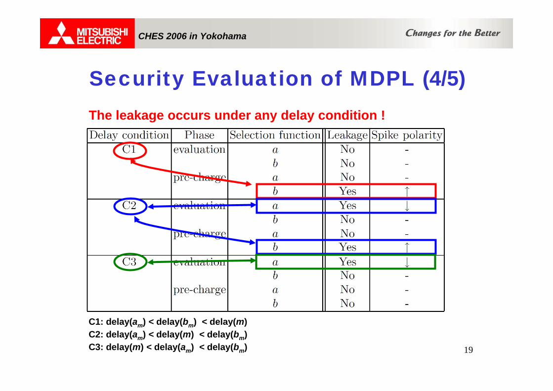
Security Evaluation of MDPL (4/5)
C1: delay(am) < delay(bm) < delay(m)C2: delay(am) < delay(m) < delay(bm)C3: delay(m) < delay(am) < delay(bm)
The leakage occurs under any delay condition !

20
CHES 2006 in Yokohama
Security Evaluation of MDPL (5/5)
C1: delay(am) < delay(bm) < delay(m)C2: delay(am) < delay(m) < delay(bm)C3: delay(m) < delay(am) < delay(bm)
The spike polarity is fixed in each phase.

21
CHES 2006 in Yokohama
Experimental Results on FPGA (1/7)
The model circuit used for our evaluation

22
CHES 2006 in Yokohama
Experimental Results using FPGA (2/7)
E1: Difference in loading capacitance(Comparison between WDDL and MDPL)
We evaluate following two setting:
E2: Difference in delay time between input signals(Relation between delay time and leakage)
We use a variety of constraints in the place-and-route to the circuits of WDDL and that of MDPL respectively.We implement each circuit and run DPA.We compare the obtained DPA traces of WDDL and MDPL.
We insert delay elements (LUTs) into the paths of input signals of MDPL gates to satisfies the delay conditions (C1 - C3). We implement each circuit and run DPA.We compare DPA traces of MDPL obtained from E1 and E2.

23
CHES 2006 in Yokohama
Experimental Results using FPGA (3/7)
DPA trace(Constraint 1)
DPA trace(Constraint 2)
DPA trace(Constraint 3)
Average Power (x 1/20)
Evaluation Phase Pre-Charge Phase
Voltage(0.4mV/div)
Time (2.0ms/div) 250MHz sampling
E1 : DPA traces of WDDL AND gates
24
CHES 2006 in Yokohama
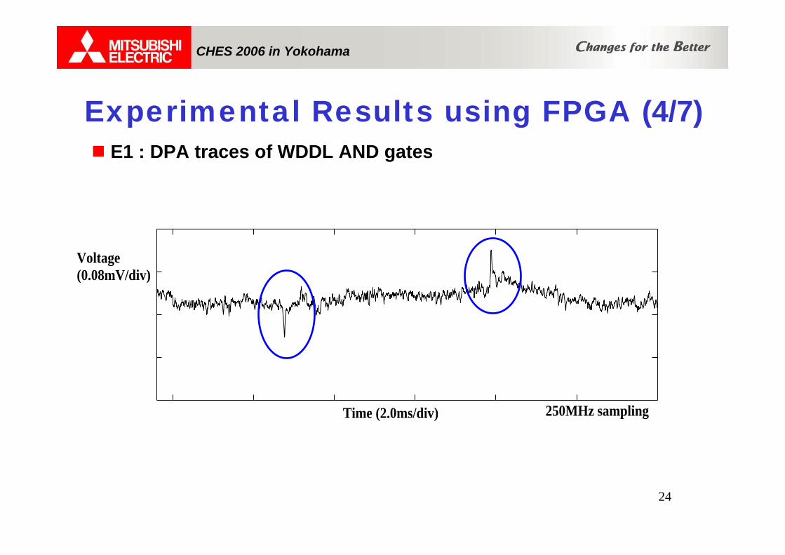
Experimental Results using FPGA (4/7)E1 : DPA traces of WDDL AND gates
Time (2.0ms/div) 250MHz sampling
Voltage(0.08mV/div)

25
CHES 2006 in Yokohama
DPA trace(Constraint 1)
DPA trace(Constraint 2)
DPA trace(Constraint 3)
Average Power (x 1/20)
Evaluation Phase Pre-Charge Phase
Voltage(0.4mV/div)
Time (2.0ms/div) 250MHz sampling
Experimental Results using FPGA (5/7)E1 : DPA traces of MDPL AND gates

26
CHES 2006 in Yokohama
Experimental Results using FPGA (6/7)E1 : DPA traces of MDPL AND gates
Time (2.0ms/div) 250MHz sampling
Voltage(0.08mV/div)

27
CHES 2006 in Yokohama
Evaluation Phase Pre-Charge Phase
<Delay Condition C1>
DPA selection function = a
DPA selection function = b
<Delay Condition C2>
<Delay Condition C3>
DPA selection function = a
DPA selection function = b
DPA selection function = a
DPA selection function = b
Average Power (x 1/20)
Voltage(0.8mV/div)
Time (2.0ms/div)Time (2.0ms/div) 250MHz sampling
Experimental Results using FPGA (7/7)E2 : DPA traces of MDPL AND gates

28
CHES 2006 in Yokohama

29
CHES 2006 in Yokohama
We evaluated previously known countermeasures using DRP logic style.
MDPL[9]
WDDL[6]
Loading capacitance
: secure under extra constraints
Conclusion
LSI designers need to adjust the delay of signals.
Delay time between input signals
: secure without extra constraints

30
CHES 2006 in Yokohama
Thanks for Listening