Embed Size (px)
Citation preview
University of Surrey07 December 2005
(1)
SEE Analysis and Mitigation forFPGA and Digital ASIC DevicesSEE Analysis and Mitigation forFPGA and Digital ASIC Devices
University of Surrey07 December 2005
Roland WeigandEuropean Space Agency
Data Systems Division TEC-EDMMicroelectronics Section
Tel. +31-71-565-3298Fax. +31-71-565-6791
Roland.Weigand[at]esa.int

University of Surrey07 December 2005
(2)
IntroductionIntroductionThe Technical and Quality Management Directorate (TEC)
http://www.esa.int/techresources/index.htmlin TEC, mainly 3 sections work on SEE effects:
The Space Environments and Effects SectionAnalysis of space environments and their effects on space systems http://space-env.esa.int/index.html
The Radiation Effects and Analysis Techniques Section Analysis at component level and radiation testinghttps://escies.org/public/radiation/esa/
The Microelectronics Section Availability of appropriate technologies and development methodsAvailability of space-specific standard components and IPDevelopment support to projectsAnalysis and mitigation of SEE at design levelhttp://www.estec.esa.nl/microelectronics/
University of Surrey07 December 2005
(3)
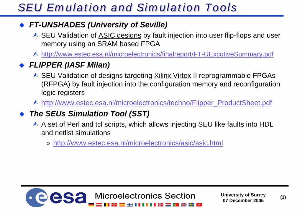
SEU Emulation and Simulation ToolsSEU Emulation and Simulation ToolsFT-UNSHADES (University of Seville)
SEU Validation of ASIC designs by fault injection into user flip-flops and user memory using an SRAM based FPGAhttp://www.estec.esa.nl/microelectronics/finalreport/FT-UExcutiveSummary.pdf
FLIPPER (IASF Milan)SEU Validation of designs targeting Xilinx Virtex II reprogrammable FPGAs (RFPGA) by fault injection into the configuration memory and reconfiguration logic registershttp://www.estec.esa.nl/microelectronics/techno/Flipper_ProductSheet.pdf
The SEUs Simulation Tool (SST)A set of Perl and tcl scripts, which allows injecting SEU like faults into HDL and netlist simulations
» http://www.estec.esa.nl/microelectronics/asic/asic.html
University of Surrey07 December 2005
(4)
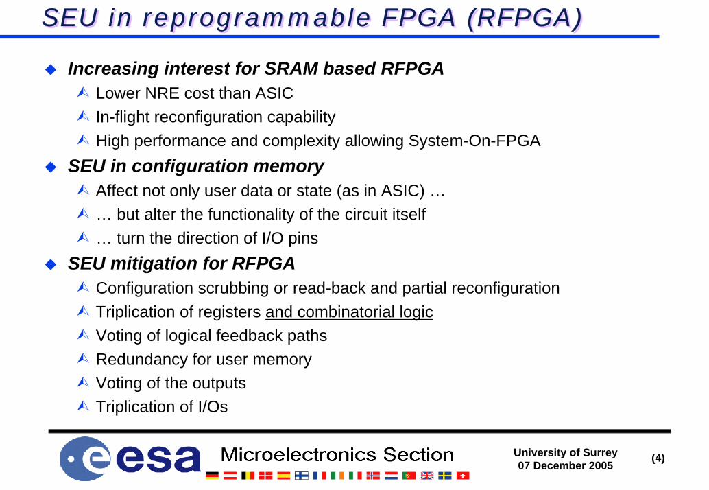
SEU in reprogrammable FPGA (RFPGA)SEU in reprogrammable FPGA (RFPGA)
Increasing interest for SRAM based RFPGALower NRE cost than ASICIn-flight reconfiguration capabilityHigh performance and complexity allowing System-On-FPGA
SEU in configuration memoryAffect not only user data or state (as in ASIC) …… but alter the functionality of the circuit itself… turn the direction of I/O pins
SEU mitigation for RFPGAConfiguration scrubbing or read-back and partial reconfigurationTriplication of registers and combinatorial logicVoting of logical feedback pathsRedundancy for user memoryVoting of the outputsTriplication of I/Os
University of Surrey07 December 2005
(5)
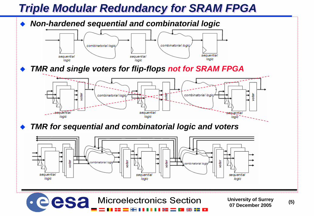
Non-hardened sequential and combinatorial logic
TMR and single voters for flip-flops not for SRAM FPGA
TMR for sequential and combinatorial logic and voters
Triple Modular Redundancy for SRAM FPGATriple Modular Redundancy for SRAM FPGA
University of Surrey07 December 2005
(6)
SEU mitigation in reprogrammable FPGASEU mitigation in reprogrammable FPGASEE mitigation by design for commercial RFPGA
Functional Triple Modular Redundancy (FTMR) – combinatorial and sequential triplication and voting in implemented in VHDL source code
» http://www.estec.esa.nl/microelectronics/techno/reprofpga.htmlFuture projects TBD: evaluate Xilinx XTMR, design a scrubbing controller IP
Xilinx SEE Consortium (USA and Europe/International)“A voluntary group of organizations that have a mutual interest in the evaluation of reconfigurable FPGAs for Aerospace Applications”
» http://www.cad.polito.it/research/consortium.html» http://www.xilinx.com/products/silicon_solutions/market_specific_devices/a
ero_def/capabilities/see.htmDevelopment of SEE hardened reprogrammable FPGA
Atmel AT40KEL and the next generation 200K FPGA under CNES contract» http://www.atmel.com/dyn/products/product_card.asp?part_id=2766
Xilinx SIRF = SEU Immune Reconfigurable FPGA (RadHard-Virtex)» http://klabs.org/mapld05/presento/176_bogrow_p.ppt
University of Surrey07 December 2005
(7)
Protection of embedded SRAM blocks (1)Protection of embedded SRAM blocks (1)EDAC = Error Detection And Correction
Usually corrects single and detects multiple bit flips per memory wordRegular access required to preventing error accumulation (scrubbing)Control state machine required to rewrite corrected dataImpact on max. clock frequency (XOR tree)
Parity protection allows detection but no hardware correctionWhen redundant data is available elsewhere in the system
» Embedded cache memories (duplicates of external memory) LEON2-FT» Duplicated memories (reload correct data from replica) LEON3-FT
On error: reload in by hardware state machine or software (reboot)Proprietary solutions
ACTEL core generator: http://www.actel.com/documents/EDAC_AN.pdf» EDAC and scrubbing
XILINX XTMR: http://klabs.org/mapld05/presento/238_rezgui_p.ppt» Triplication, voting and scrubbing
Area overhead from 1 bit/word (parity) to > triple (Xilinx solution)
University of Surrey07 December 2005
(8)
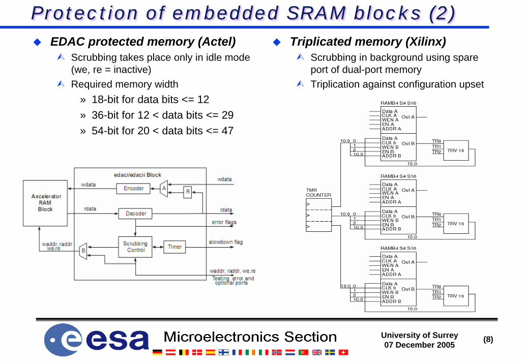
Protection of embedded SRAM blocks (2)Protection of embedded SRAM blocks (2)EDAC protected memory (Actel)
Scrubbing takes place only in idle mode (we, re = inactive)Required memory width
» 18-bit for data bits <= 12» 36-bit for 12 < data bits <= 29» 54-bit for 20 < data bits <= 47
Triplicated memory (Xilinx)Scrubbing in background using spare port of dual-port memoryTriplication against configuration upset
University of Surrey07 December 2005
(9)
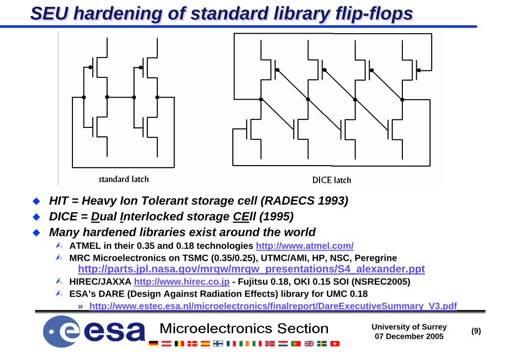
SEU hardening of standard library flip-flopsSEU hardening of standard library flip-flops
HIT = Heavy Ion Tolerant storage cell (RADECS 1993)DICE = Dual Interlocked storage CEll (1995)Many hardened libraries exist around the world
ATMEL in their 0.35 and 0.18 technologies http://www.atmel.com/MRC Microelectronics on TSMC (0.35/0.25), UTMC/AMI, HP, NSC, Peregrine
http://parts.jpl.nasa.gov/mrqw/mrqw_presentations/S4_alexander.pptHIREC/JAXXA http://www.hirec.co.jp - Fujitsu 0.18, OKI 0.15 SOI (NSREC2005)ESA’s DARE (Design Against Radiation Effects) library for UMC 0.18
» http://www.estec.esa.nl/microelectronics/finalreport/DareExecutiveSummary_V3.pdf
University of Surrey07 December 2005
(10)
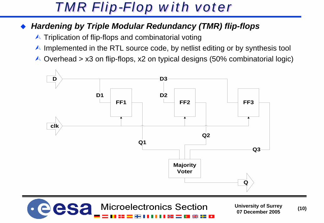
TMR Flip-Flop with voterTMR Flip-Flop with voterHardening by Triple Modular Redundancy (TMR) flip-flops
Triplication of flip-flops and combinatorial votingImplemented in the RTL source code, by netlist editing or by synthesis toolOverhead > x3 on flip-flops, x2 on typical designs (50% combinatorial logic)
FF1 FF2 FF3
MajorityVoter
Q1Q2
Q3
D1 D2
D3
clk
D
Q
University of Surrey07 December 2005
(11)
Single Event Transients (SET)Single Event Transients (SET)Collision induced carrier generation in PN junctions
Propagate as glitches in combinatorial logicLatched into storage cells when arriving at data input during clock edge
Upset rate increases with the clock frequencyMain SEE in ERC32 processor (0.5 µm technology)… definitely a concern in 0.18 µm and below
Analysis of SET effects in simulation and radiation testsSET pulse length and amplitude are most important parametersSpecific test structures to catch and characterise the pulseCNES contract with Atmel on SET effects in the 0.18 µm technology
Mitigation of SET effectshttp://www.mrchsv.com/docs/Vanderbilt/Circuit%20and%20layout%20Issues.pdfPropagation of complementary logic levels (“Dual Stream”)Using stronger drivers and higher capacitive loadsDelay filtering on all flip-flop inputs (clock, data, reset)Temporal Vote: Triple skewed clocks in conjunction with the TMR flip-flop
» Triplication of clock-like nets (including asynchronous resets)
University of Surrey07 December 2005
(12)
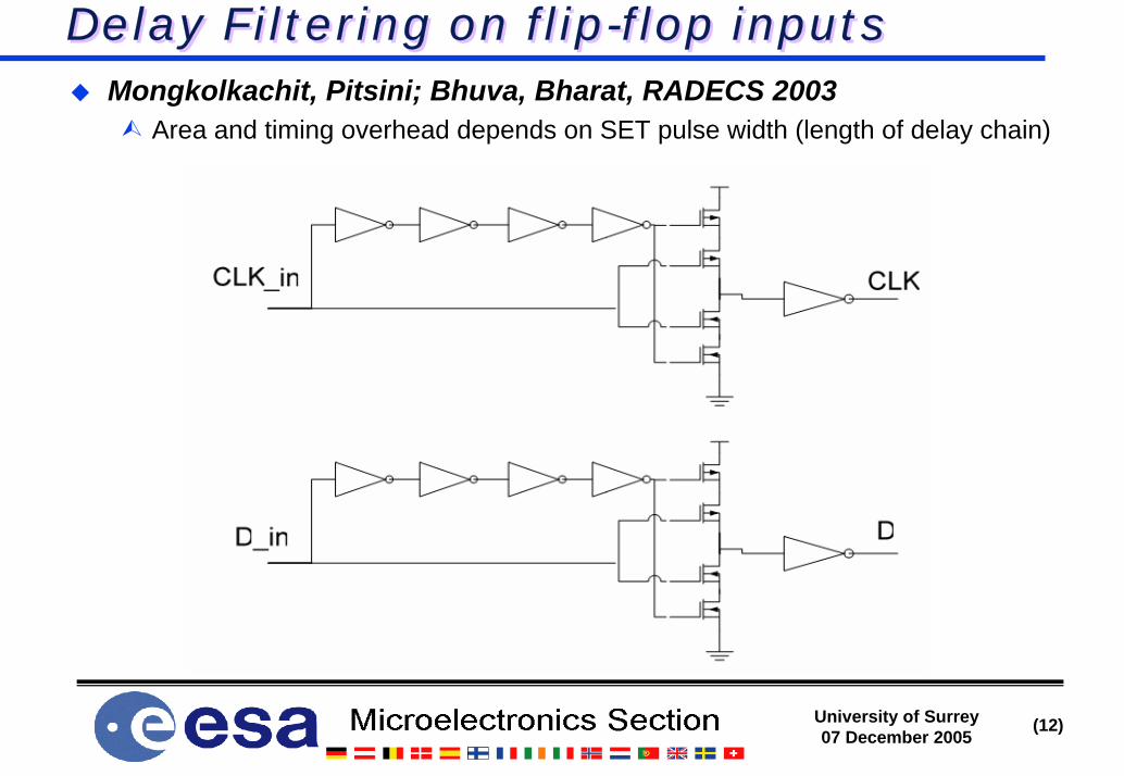
Delay Filtering on flip-flop inputsDelay Filtering on flip-flop inputsMongkolkachit, Pitsini; Bhuva, Bharat, RADECS 2003
Area and timing overhead depends on SET pulse width (length of delay chain)
University of Surrey07 December 2005
(13)
SET-tolerance by skewed clocksSET-tolerance by skewed clocks
δ
FF1 FF2 FF3
MajorityVoter
Q1
Q2
Q3
clock tree 3
clocktree 2
clocktree 1
D1 D2
D3
clk
D
Q
δ
clk2
clk1
clk3
SET pulse
SET latched intoFF1 only
Q remains at correct valueTriplicated clock tree
and skewed clocks
δ ~ SET pulse length
University of Surrey07 December 2005
(14)
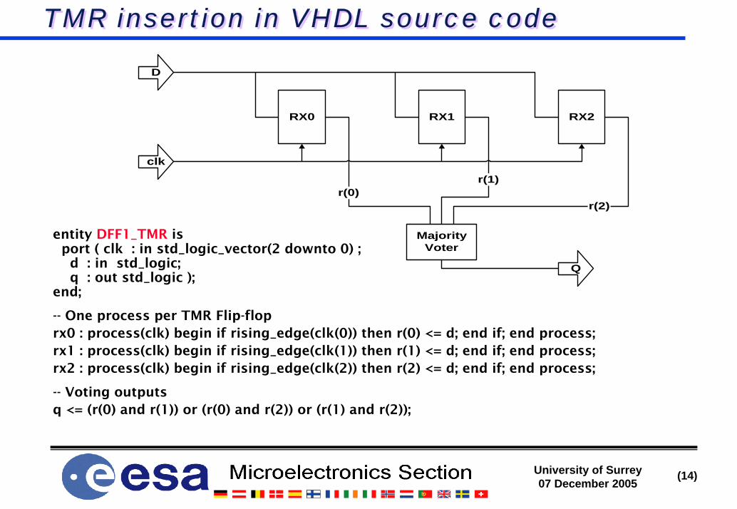
TMR insertion in VHDL source codeTMR insertion in VHDL source code
entity DFF1_TMR is port ( clk : in std_logic_vector(2 downto 0) ;
d : in std_logic; q : out std_logic );
end;
-- One process per TMR Flip-floprx0 : process(clk) begin if rising_edge(clk(0)) then r(0) <= d; end if; end process;rx1 : process(clk) begin if rising_edge(clk(1)) then r(1) <= d; end if; end process;rx2 : process(clk) begin if rising_edge(clk(2)) then r(2) <= d; end if; end process;
-- Voting outputs q <= (r(0) and r(1)) or (r(0) and r(2)) or (r(1) and r(2));
RX0 RX1 RX2
MajorityVoter
r(0)r(1)
r(2)
clk
D
Q
University of Surrey07 December 2005
(15)
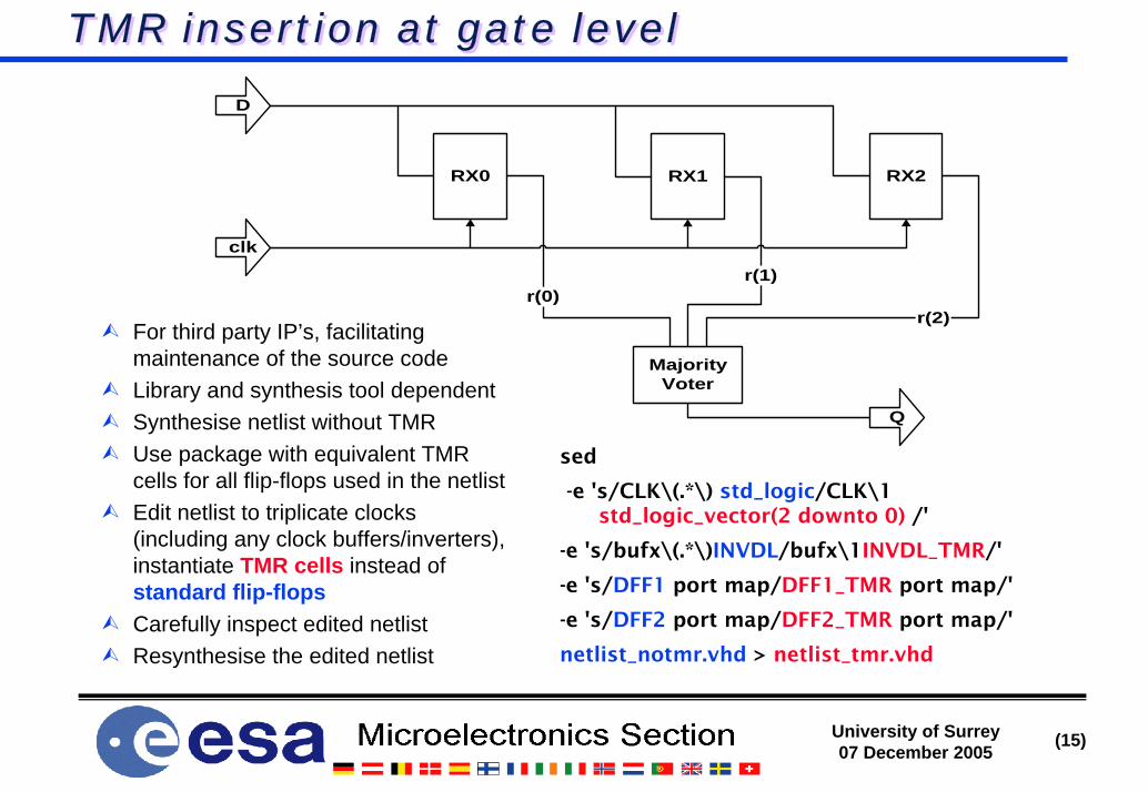
TMR insertion at gate levelTMR insertion at gate level
RX0 RX1 RX2
MajorityVoter
r(0)r(1)
r(2)
clk
D
Q
For third party IP’s, facilitating maintenance of the source codeLibrary and synthesis tool dependentSynthesise netlist without TMRUse package with equivalent TMR cells for all flip-flops used in the netlistEdit netlist to triplicate clocks (including any clock buffers/inverters), instantiate TMR cells instead of standard flip-flopsCarefully inspect edited netlistResynthesise the edited netlist
sed
-e 's/CLK\(.*\) std_logic/CLK\1 std_logic_vector(2 downto 0) /'
-e 's/bufx\(.*\)INVDL/bufx\1INVDL_TMR/'
-e 's/DFF1 port map/DFF1_TMR port map/'
-e 's/DFF2 port map/DFF2_TMR port map/'
netlist_notmr.vhd > netlist_tmr.vhd
University of Surrey07 December 2005
(16)
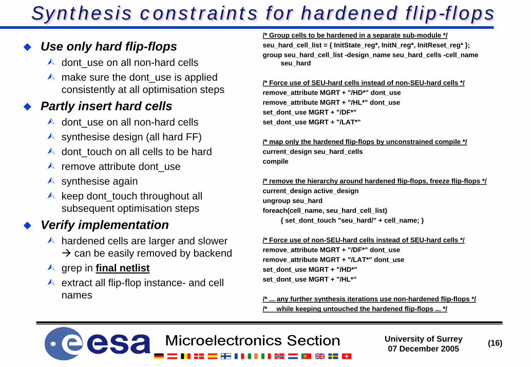
Synthesis constraints for hardened flip-flopsSynthesis constraints for hardened flip-flops
Use only hard flip-flopsdont_use on all non-hard cellsmake sure the dont_use is applied consistently at all optimisation steps
Partly insert hard cellsdont_use on all non-hard cellssynthesise design (all hard FF)dont_touch on all cells to be hardremove attribute dont_usesynthesise againkeep dont_touch throughout all subsequent optimisation steps
Verify implementationhardened cells are larger and slower
can be easily removed by backend grep in final netlistextract all flip-flop instance- and cell names
/* Group cells to be hardened in a separate sub-module */seu_hard_cell_list = { InitState_reg*, InitN_reg*, InitReset_reg* };group seu_hard_cell_list -design_name seu_hard_cells -cell_name
seu_hard
/* Force use of SEU-hard cells instead of non-SEU-hard cells */remove_attribute MGRT + "/HD*" dont_useremove_attribute MGRT + "/HL*" dont_useset_dont_use MGRT + "/DF*"set_dont_use MGRT + "/LAT*"
/* map only the hardened flip-flops by unconstrained compile */current_design seu_hard_cellscompile
/* remove the hierarchy around hardened flip-flops, freeze flip-flops */current_design active_designungroup seu_hardforeach(cell_name, seu_hard_cell_list)
{ set_dont_touch "seu_hard/" + cell_name; }
/* Force use of non-SEU-hard cells instead of SEU-hard cells */remove_attribute MGRT + "/DF*" dont_useremove_attribute MGRT + "/LAT*" dont_useset_dont_use MGRT + "/HD*"set_dont_use MGRT + "/HL*"
/* ... any further synthesis iterations use non-hardened flip-flops *//* while keeping untouched the hardened flip-flops ... */
University of Surrey07 December 2005
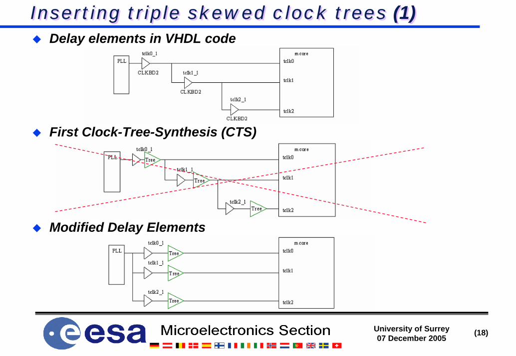
(17)
Inserting triple skewed clock trees (1)Inserting triple skewed clock trees (1)Clock Tree Synthesis (CTS) is part of backend (layout) design
Triple CTS critical when many clock domains existCTS guarantees only max clock skew inside a clock treeDifferent latency (delay from source to flip-flop) in different clock trees
Delay insertion at the origin of the clock treesDelays are not synthesisableInstantiate delay buffers in the VHDL source code
speculative, needs control and adjustment in the backend processIn the backend process along with the CTS
Delay insertion in the flip-flopsArea consumingOnly one clock tree (easy design flow)No SET mitigation in the clock tree
Triplication of reset treesAsynchronous resets are clock-like signals
University of Surrey07 December 2005
(18)
Delay elements in VHDL code
First Clock-Tree-Synthesis (CTS)
Modified Delay Elements
Inserting triple skewed clock trees (1)Inserting triple skewed clock trees (1)
University of Surrey07 December 2005
(19)
SEU mitigation in the ASIC design flowSEU mitigation in the ASIC design flow
Increased complexity affects the design flow and –resultsLarge netlist with higher cell and node countIncreased run-time or even crashes of EDA toolsDesign optimisation is less efficient
Synthesis tools are designed to remove redundancyNormally, registers are not modified – but be careful …… with sequential optimisation (pipelining, retiming etc.)
Timing issuesTMR voting and clock skewing reduces maximum speedIncreased area leads to higher interconnect delayClock skewing can be removed by hold-time fix
Verification and test issuesTMR and formal verification (1 FF in RTL 3 FF at gate level)TMR (= redundancy) affects testability in scan testingImplementation of protection has to be verified at netlist level
University of Surrey07 December 2005
(20)
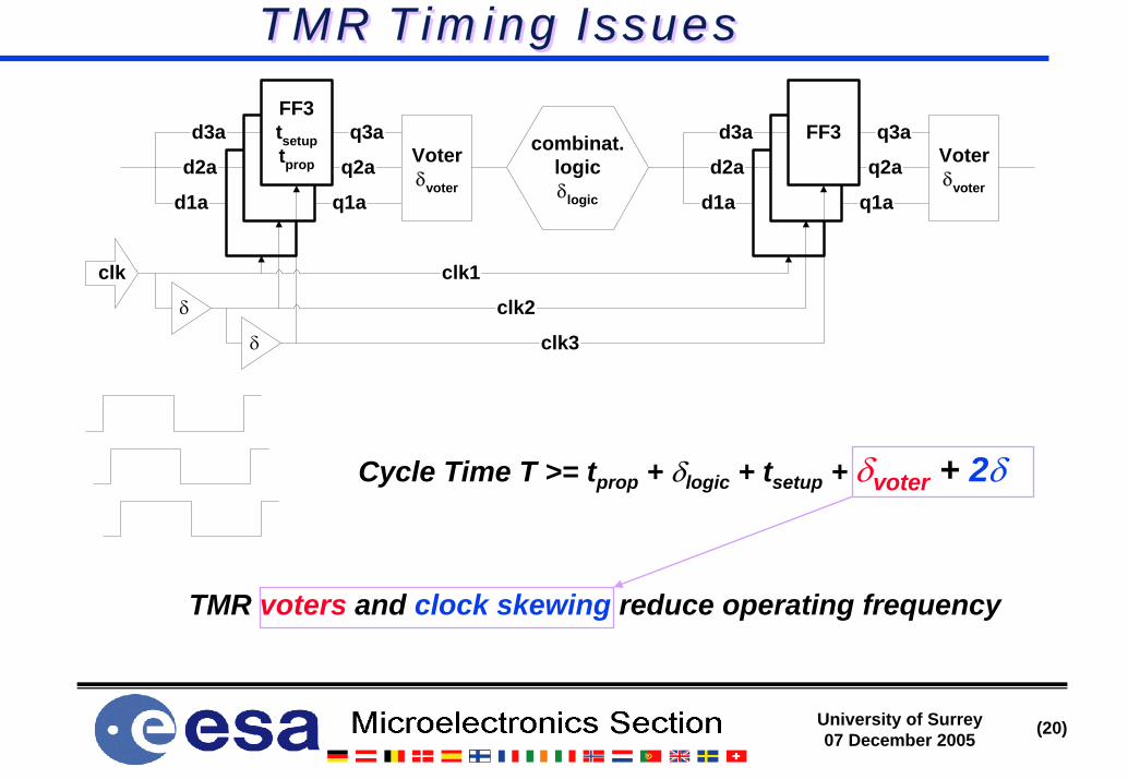
TMR Timing IssuesTMR Timing Issues
TMR voters and clock skewing reduce operating frequency
q2a
q1aFF1
FF2
FF3tsetuptprop Voter
δvoter
q3a
d1a
d2a
d3a
q2a
q1aFF1
FF2
FF3Voterδvoter
q3a
d1a
d2a
d3a
clk3
clk2
clk1clk
δ
δ
combinat.logicδlogic
Cycle Time T >= tprop + δlogic + tsetup + δvoter + 2δ
University of Surrey07 December 2005
(21)
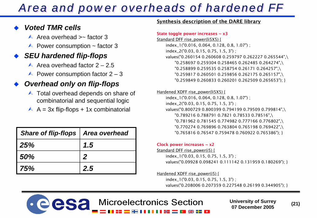
Area and power overheads of hardened FFArea and power overheads of hardened FF
Voted TMR cellsArea overhead >~ factor 3Power consumption ~ factor 3
SEU hardened flip-flopsArea overhead factor 2 – 2.5Power consumption factor 2 – 3
Overhead only on flip-flopsTotal overhead depends on share of combinatorial and sequential logicA = 3x flip-flops + 1x combinatorial
Synthesis description of the DARE library
State toggle power increases ~ x3
Standard DFF rise_power(li5X5) {index_1("0.016, 0.064, 0.128, 0.8, 1.07") ;index_2("0.03, 0.15, 0.75, 1.5, 3") ;values("0.260154 0.260608 0.259797 0.262227 0.265544",\
"0.258697 0.259304 0.258465 0.262485 0.264274",\"0.258899 0.259535 0.258754 0.26171 0.264257",\"0.259817 0.260501 0.259856 0.262175 0.265157",\"0.259849 0.260833 0.260201 0.262509 0.265653"); }
Hardened XDFF rise_power(li5X5) {index_1("0.016, 0.064, 0.128, 0.8, 1.07") ; index_2("0.03, 0.15, 0.75, 1.5, 3") ;values("0.800729 0.800399 0.794199 0.79509 0.799814",\
"0.789216 0.788791 0.7821 0.78533 0.78516",\"0.781962 0.781545 0.774982 0.777166 0.776802",\"0.770274 0.769896 0.763804 0.765198 0.769422",\"0.765816 0.76547 0.759478 0.760922 0.765386"); }
Clock power increases ~ x2
Standard DFF rise_power(i5) {index_1("0.03, 0.15, 0.75, 1.5, 3") ;values("0.09928 0.098241 0.111142 0.131959 0.180269"); }
Hardened XDFF rise_power(i5) {index_1("0.03, 0.15, 0.75, 1.5, 3") ;values("0.208006 0.207359 0.227548 0.26199 0.344905"); }
Share of flip-flops Area overhead
25% 1.550% 275% 2.5
University of Surrey07 December 2005
(22)
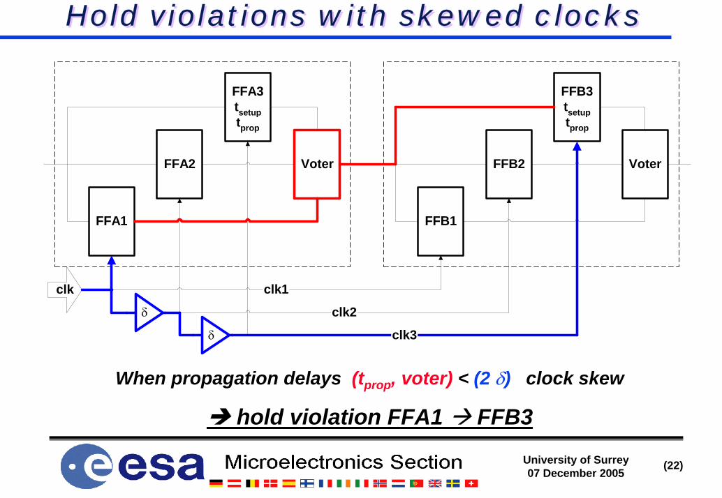
Hold violations with skewed clocksHold violations with skewed clocks
When propagation delays (tprop, voter) < (2 δ) clock skew
hold violation FFA1 FFB3
clk3
clk2
clk1clk
δ
FFA1
FFA2
FFA3tsetuptprop
Voter
FFB1
FFB2
FFB3tsetuptprop
Voter
δ
University of Surrey07 December 2005
(23)
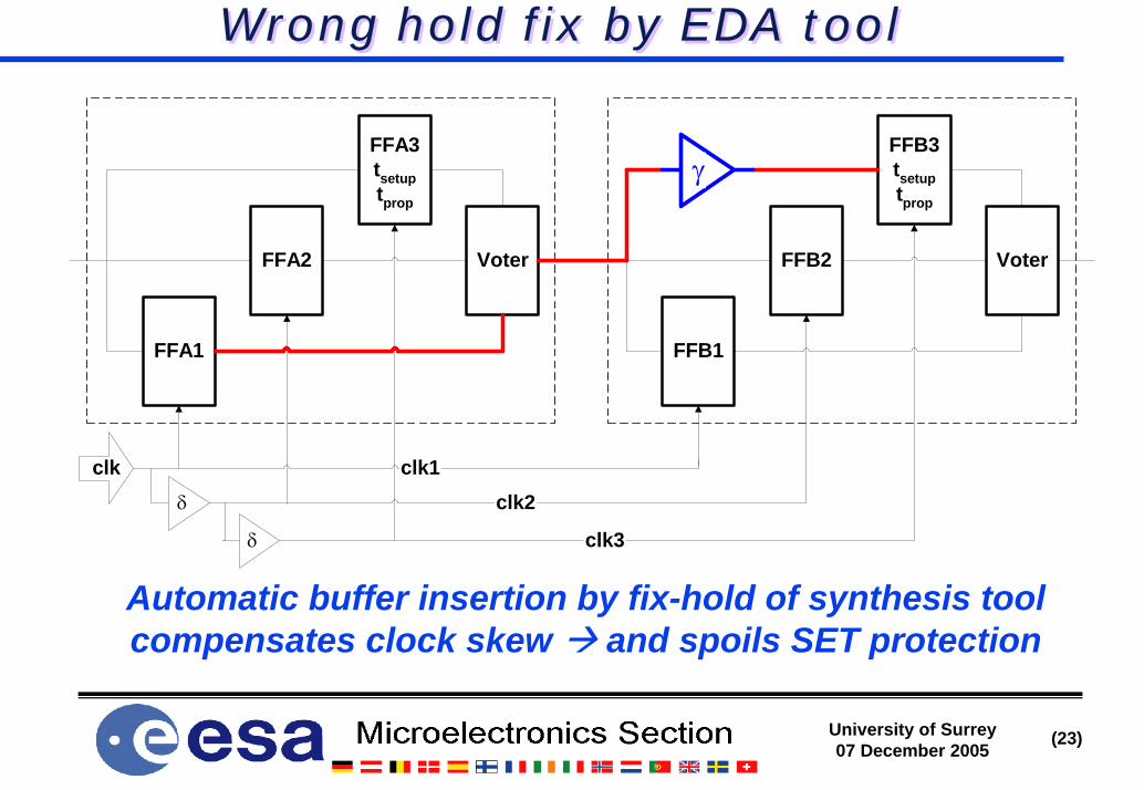
Wrong hold fix by EDA toolWrong hold fix by EDA tool
Automatic buffer insertion by fix-hold of synthesis tool compensates clock skew and spoils SET protection
clk3
clk2clk1clk
δ
δ
FFA1
FFA2
FFA3tsetuptprop
Voter
FFB1
FFB2
FFB3tsetuptprop
Voter
γ
University of Surrey07 December 2005
(24)
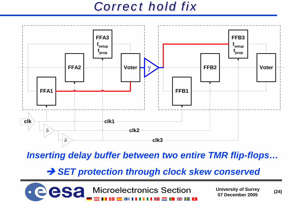
Correct hold fixCorrect hold fix
Inserting delay buffer between two entire TMR flip-flops…
SET protection through clock skew conserved
clk3
clk2clk1clk
δ
δ
FFA1
FFA2
FFA3tsetuptprop
Voter
FFB1
FFB2
FFB3tsetuptprop
Voterγ
University of Surrey07 December 2005
(25)
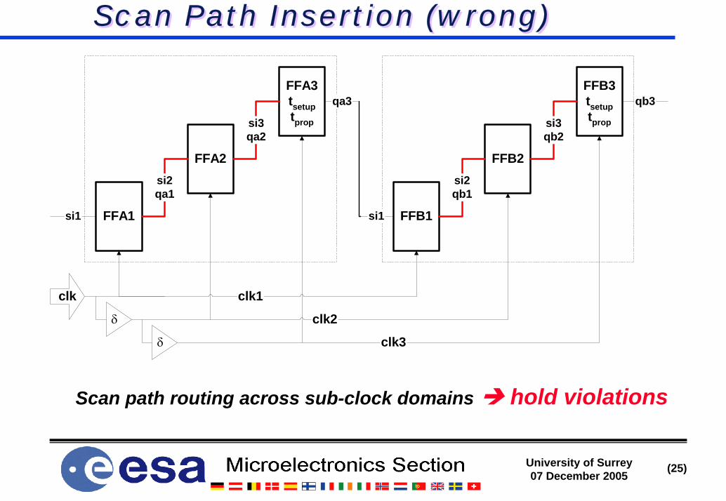
Scan Path Insertion (wrong)Scan Path Insertion (wrong)
clk3
clk2
clk1clk
δ
δ
FFA1
FFA2
FFA3tsetuptprop
si2qa1
si3qa2
qa3
si1 FFB1
FFB2
FFB3tsetuptprop
si2qb1
si3qb2
qb3
si1
Scan path routing across sub-clock domains hold violations
University of Surrey07 December 2005
(26)
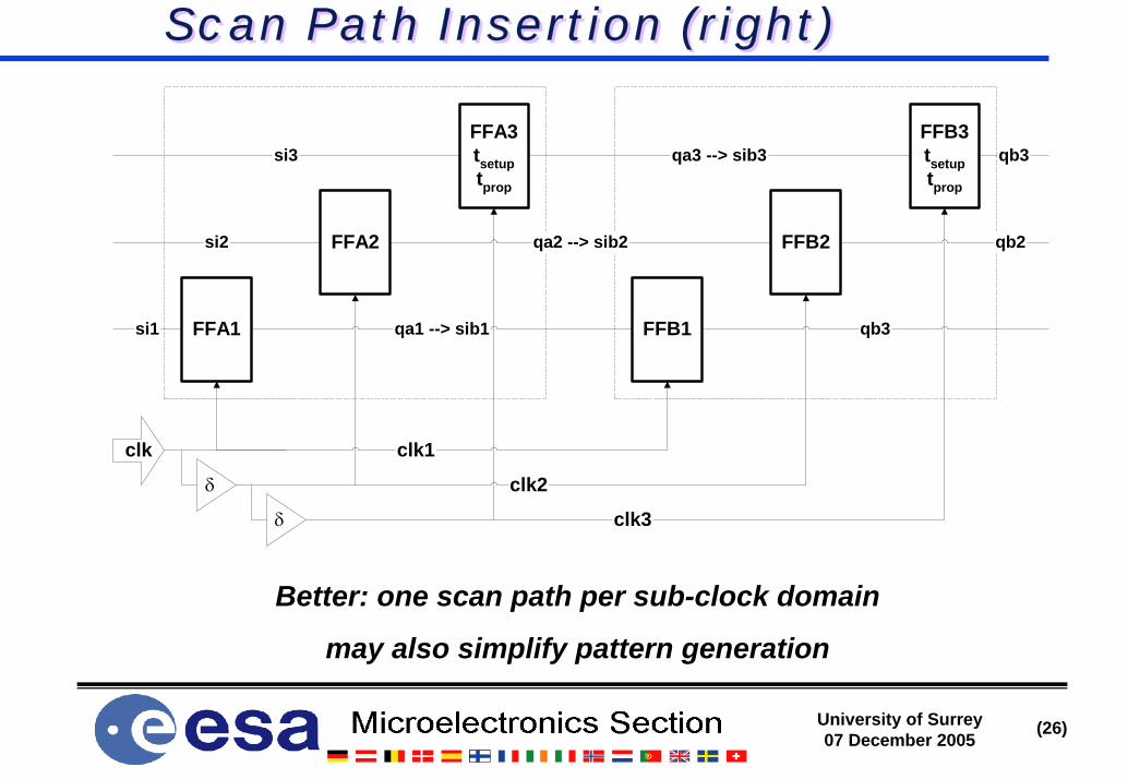
Scan Path Insertion (right)Scan Path Insertion (right)
clk3
clk2
clk1clk
δ
δ
FFA1
FFA2
FFA3tsetuptprop
si2
si3 qa3 --> sib3
si1 FFB1
FFB2
FFB3tsetuptprop
qa2 --> sib2 qb2
qb3
qa1 --> sib1 qb3
Better: one scan path per sub-clock domain
may also simplify pattern generation
University of Surrey07 December 2005
(27)
Future perspectivesFuture perspectives
SEU protected flip-flops available for many technologies… but SET protection is currently in experimental stadium
SEU and SET protected flip-flop as library cellsDF-DICE http://www.isi.edu/~draper/papers/mwscas05_bhatti.pdf
If not available - workaround: build SET flip-flop as macrocellCompose TMR with triple clock input out of standard library cellsGenerate appropriate front-end synthesis library for the TMR cellReplace TMR macrocells by standard cell triplet in the gate-level netlistPlace and Route with standard foundry design flow
AdvantagesCan be implemented with a standard vendor libraryNo need to modify design at source code levelAvoids many problems with design flow and tools
IssuesConstraints on backend flow (freeze the SET-cell for timing and hold-fix)Triple skewed clock and triple reset trees
University of Surrey07 December 2005
(28)
ConclusionConclusionSEU and SET protection possible with commercial ASIC technologyRefresh/scrubbing against accumulation of (uncorrectable) upsetsPitfalls in the design flow with commercial EDA tools
Requires workarounds, scripting and proper constrainingHardened flip-flops easier to use than building TMR in source code
Hardened library cells, Macrocells composed of commercial library cellsBut there will always be a price to pay (speed, area, power…)Is full SEU protection always necessary?
Determine upset rate of a given design (sub-function) in a given orbitDetermine the impact of an upset at system levelApply selective use of SEU protection
Contact us… http://www.estec.esa.int/microelectronics
Questions?


![ASIC Design & FPGA-1st Chapter[1]](https://img.pdfslide.net/doc/110x75/577d203f1a28ab4e1e925961/asic-design-fpga-1st-chapter1.jpg)