Embed Size (px)
Citation preview
ROYAL INSTITUTE OF TECHNOLOGY
Selective Epitaxy of Indium Phosphide and Heteroepitaxy of Indium Phosphide
on Silicon for Monolithic Integration
Doctoral Thesis by
Fredrik Olsson
Laboratory of Semiconductor Materials
School of Information and Communication Technology Royal Institute of Technology (KTH)
Stockholm 2008
Selective epitaxy of indium phosphide and heteroepitaxy of indium phosphide on silicon for monolithic integration A dissertation submitted to the Royal Institute of Technology, Stockholm, Sweden, in partial fulfillment of the requirements for the degree of Doctor of Philosophy. TRITA-ICT/MAP AVH Report 2008:11 ISSN 1653-7610 ISRN KTH/ICT-MAP/AVH-2008:11-SE ISBN 978-91-7178-991-4 © Fredrik Olsson, June 2008 Printed by Universitetsservice US-AB, Stockholm 2008 Cover Picture: Microscopy photograph of RIE etched and HVPE regrown waveguide structures showing near to perfect planarization.
ii
Fredrik Olsson: Selective epitaxy of indium phosphide and heteroepitaxy of indium phosphide on silicon for monolithic integration TRITA-ICT/MAP AVH Report 2008:11, ISSN 1653-7610, ISRN KTH/ICT-MAP/AVH-2008:11-SE, ISBN 978-91-7178-991-4 Royal Institute of Technology (KTH), School of Information and Communication Technology, Laboratory Semiconductor Materials
Abstract
A densely and monolithically integrated photonic chip on indium phosphide is greatly in need for data transmission but the present day’s level of integration in InP is very low. Silicon enjoys a unique position among all the semiconductors in its level of integration. But it suffers from its slow signal transmission between the circuit boards and between the chips as it uses conventional electronic wire connections. This being the bottle-neck that hinders enhanced transmission speed, optical-interconnects in silicon have been the dream for several years. Suffering from its inherent deficient optical properties, silicon is not supposed to offer this feasibility in the near future. Hence, integration of direct bandgap materials, such as indium phosphide on silicon, is one of the viable alternatives. This thesis addresses these two issues, namely monolithic integration on indium phosphide and monolithic integration of indium phosphide on silicon. To this end, we use two techniques, namely selective epitaxy and heteroepitaxy by employing hydride vapor phase epitaxy method.
The first part deals with the exploitation of selective epitaxy for fabricating a discrete and an integrated chip based on InP. The former is a multi-quantum well buried heterostructure laser emitting at 1.55 µm that makes use of AlGaInAs and InGaAsP as the barrier and well, respectively. We demonstrate that even though it contains Al in the active region, semi-insulating InP:Fe can be regrown. The lasers demonstrate threshold as low as 115A/cm2/quantum well, an external quantum efficiency of 45% and a characteristic temperature of 78 K, all at 20 oC. Concerning the integrated device, we demonstrate complex and densely packed buried arrayed waveguide (AWG) structures found in advanced systems-on-the-chip for optical code-division multiple-access (O-CDMA). We present a case of an error-free 10 Gb/s encoding and decoding operation from an eight-channel AWGs with 180 GHz channel spacing. Selective epitaxial growth aspects specific to these complicated structures are also described and guidance on design implementation of these AWGs is given. Mass transport studies on these AWGs are also presented.
The second part deals with various studies on and relevant to epitaxial lateral overgrowth (ELOG) of high quality InP on silicon. (i) ELOG often encounters cases where most part of the surface is covered by mask. From the modeling on large mask area effects, their impact on the transport and kinetic properties has been established. (ii) It is known that ELOG causes strain in the materials. From synchrotron X-ray measurements, strain is shown to have large effect on the mask edges and the underlying substrate. (iii) The combination of strain and the influence of image forces when reducing the opening dimensions in ELOG has been modeled. It is found to be very beneficial to reduce openings down to ~100 nm where effective filtering of dislocations is predicted to take place even in vicinity of the openings. We call it nano-ELOG. (iv) By combining the modeling results of nano-ELOG and of a pre-study of ELOG on pure InP, a novel net pattern design is invented and experimented for nano-ELOG of InP on Si. PL measurements together with transmission electron microscopy observations indicate beneficial effects of small size openings (200 nm) compared to 1000 nm openings. (v) ELOG of InP on silicon-on-insulators together with a multi-quantum well structure grown on it has been demonstrated for the first time. This is particularly interesting for integrating silicon/silicon dioxide waveguides with InP.
iii
Acknowledgments
This thesis would not have been possible without the support from colleagues, friends and family. First of all I would like to express my deepest gratitude to my supervisor, Prof. Sebastian Lourdudoss whose guidance, never ending positive attitude and enthusiasm have helped me a lot. I admire you and I am grateful for the friendship that we have developed during the period of this thesis. I also would like to express special thanks to Gunnar Andersson who has been invaluable when it comes to fix and repair the equipments in the lab. He is the perfect personification of the engineering character found in the books of Jules Verne. I also want to thank Prof. Gunnar Landgren who kindly employed me as a Ph.D. student.
There are many more members, or former members, in the HMA group to whom I would like to give special thanks. Dr. Yan-Ting Sun who introduced me to the HVPE equipment, Dr. Carlos Angulo Barrios who taught me processing, Dr. Anand Srinivasan for several scientific and other nice discussions at KTH and in the Pendeltåg, Prof. Mattias Hammar for nice discussions during lunches, Dr. Henry Radamson for teaching me HRXRD and many occasional discussions, Dr. Thomas Aggerstam with whom I been sharing the same office for many years and have had interesting chats about everything, Jesper Berggren for funny chats at the epitaxy equipments and help with the computer, Dr. Rickard Marcks von Würtemberg and Dr. Petrus Sundgren for many occasional discussions and chats both during lunches and in the lab. Many thanks to Marianne Widing who is so kind and really a heroine when it comes to help with the administrative issues.
During the period of this thesis, I have had the occasion to have several international collaborations. I would like to thank Prof. S. Ben Yoo and his group (University of California at Davis, USA) with whom I have had a very long and fruitful collaboration; I was given a very interesting and challenging work in conducting regrowth of complex components for O-CDMA. I was also hosted by him on two occasions. I also benefited from my participation in the European Network of Excellence, PHOREMOST, where I interacted with several people including Prof. Pablo Aitor Postigo and his group (Instituto de Microelectronica de Madrid (CSIC), Madrid, Spain), Prof. Marco Malvezzi, University of Pavia and Prof. Csilla Gergely, Université de Montpellier-II. Many thanks to Prof. Pablo Postigo for helping me with e-beam processing and hosting me in his lab. Many thanks to Prof. Juan Jiménez, and Dr. Manuel Avella (ETSII, Valladolid, Spain) for their excellent and valuable help on material characterization, and also many thanks to Prof. Ikai Lo and the friends in Taiwan (National Sun Yat-Sen University, Kaohsiung, Taiwan) who hosted me, created an unforgettable atmosphere for me and helped me with TEM measurements.
I am very grateful to the rest of the members of HMA during my time here for creating a friendly and helpful atmosphere: Ming-Hong Gau, Dr. Mikael Mulot, Dr. Carl Asplund, Carl Junesand, Oscar Gustafsson, Dr. Olivier Douheret, Dr. Carlos Angulo Barrios, Dr. Audrey Berrier, Peter Goldmann, Mikael Sjödin, Yu Xingang , Shangufta Naureen, Naeem Shahid, Dr. Yaocheng Shi, Zhenzhong Zhang, Dr. Julius Hållstedt, Dr. Sebastian Mogg, Dr. Martin Strassner, Dr. Krishnan Baskar, Dr. Kestius Maknys and Dr. Nils Nordell.
I am also very grateful to the close collaborations I have had with Master Thesis students and I would like to give many thanks to Gaël Mion, Tiankai Zhu, Amandine Aubert, Mengyao Xie, Jiayue Yuan, Leila Nahidi Azar and Xiang Yu.
iv

Finally, on the more personal level I would like to thank my parents for always being
there for me, supporting me and encouraging me and who helped me taking the right decisions earlier in my life. I also would like to give my greatest thanks to my wife who is constantly there for me with her love and encouragement in times when things around me are a little bit tough. I am also very grateful for all my friends and other relatives who are too many to be mentioned here.
v
Table of contents Abstract ............................................................................................................ iii Acknowledgments ......................................................................................... iv List of papers ................................................................................................ viii Acronyms ......................................................................................................... xi 1 Introduction................................................................................................. 1
1.1 Motivation for use of HVPE in large-scale component integration on InP .....2 1.2 Motivation for use of HVPE for realizing heteroepitaxy of InP on Si...............4
1.2.1 Why InP on Silicon?........................................................................................4 1.2.2 The main hindrance for integration of highly dissimilar materials ...........6 1.2.3 Techniques for mastering the dislocations..................................................7 1.2.4 Epitaxial lateral overgrowth and the benefits of using HVPE...................8
1.3 Major investigations of this thesis.........................................................................9 2 Background............................................................................................... 11
2.1 III-V semiconductor materials..............................................................................11 2.2 Crystallographic properties ..................................................................................11
2.2.1 Diamond lattice ..............................................................................................12 2.2.2 Zinc blende lattice .........................................................................................12 2.2.3 Miller index .....................................................................................................12
2.3 Orientation effects for zinc blende lattice ..........................................................13 2.4 Lattice constants, thermal expansion and elastic properties .........................14
2.4.1 Resolved shear stress ..................................................................................17 2.5 Epitaxial growth techniques for III-V materials .................................................18 2.6 Hydride Vapor Phase Epitaxy (HVPE)...............................................................18 2.7 The reactor system ...............................................................................................20 2.8 Dopants in HVPE ..................................................................................................21 2.9 Selective area growth (SAG) ...............................................................................22
2.9.1 Model (I) of selective area growth ..............................................................23 2.9.2 Model (II) of selective area growth – thin film model ...............................24
2.10 Defects ....................................................................................................................25 2.10.1 Impurities ........................................................................................................25 2.10.2 Dislocations ....................................................................................................25
2.10.2.1 Critical thickness....................................................................................29 2.10.2.2 Image forces ..........................................................................................29
2.10.3 Slip planes and dislocations in zinc blende lattice ...................................30 2.10.4 Planar defects ................................................................................................32
2.10.4.1 Stacking faults........................................................................................32 2.10.4.2 Twins .......................................................................................................33 2.10.4.3 Inversion Domain Boundaries (IDBs).................................................33
2.11 Characterization methods ....................................................................................34 2.11.1 High resolution X-ray diffraction..................................................................35
2.11.1.1 Strain .......................................................................................................36 2.11.2 Photoluminescence.......................................................................................36 2.11.3 Cathodoluminescence ..................................................................................38 2.11.4 Crystallographic etching ...............................................................................38 2.11.5 Transmission Electron Microscopy.............................................................38
2.12 Background on applications ................................................................................40
vi

2.12.1 Semiconductor lasers ...................................................................................40 2.12.2 Arrayed Waveguide Gratings (AWG).........................................................42
3 Summary of results and discussions ................................................ 47 3.1 Deep etching and regrowth of dense arrayed waveguide gratings...............48
3.1.1 Reactive ion etching .....................................................................................48 3.1.2 Regrowth of all-angled oriented waveguide structures ...........................50 3.1.3 Mass transport ...............................................................................................55
3.2 Regrowth and characterization of encoder/decoder for O-CDMA.................56 3.3 Regrowth and characterization of semiconductor lasers with Al in the barriers. ...............................................................................................................................58 3.4 Large mask area effects in selective epitaxy ....................................................61 3.5 ELOG of InP applied on InP-precoated exact-oriented SOI substrate. ........64 3.6 Strain and defect measurement in ELOG .........................................................66 3.7 Heteroepitaxy through nano-ELOG....................................................................68
3.7.1 Modeling and experimental results from InP on Si grown by nano-ELOG 68 3.7.2 Prestudy of ELOG of InP on InP substrates .............................................71 3.7.3 Study of ELOG of InP on Si in nano-size openings.................................73
4 Summary of appended papers ............................................................ 77 5 Summary of results, conclusions and future outlook .................. 81 References ...................................................................................................... 84
vii
List of papers Publications included in the thesis
A J. Cao, R. G. Broeke, N. K. Fontaine, C. Ji, Y. Du, N. Chubun, K. Aihara, Anh-Vu Pham, F. Olsson, S. Lourdudoss, and S. J. Ben Yoo, “Demonstration of Spectral Phase Encoding and Decoding in Monolithically Integrated O-CDMA Arrayed-Waveguide-Grating-Based Encoder”, IEEE Photon. Technol. Lett., vol. 18, no. 24, pp.2602 (2006).
B M. N. Akram, O. Kjebon, S. Marcinkevičius, R. Schatz, J. Berggren, F. Olsson, and S.
Lourdudoss, “The Effect of Barrier Composition on the Vertical Carrier Transport and Lasing Properties of 1.55 µm Multiple Quantum-Well Structures”, IEEE J. Quantum Electron., vol. 42, no. 7, pp. 712 (2006).
C F. Olsson, T. Zhu, G. Mion, and S. Lourdudoss, “Large mask area effects in selective
area growth”, J. Cryst. Growth, vol. 289, no. 1, pp. 24 (2006).
D F. Olsson, A. Aubert, M. Avella, J. Jiménez, C. A. Barrios , J. Berggren and S. Lourdudoss, ” Heteroepitaxy of InP on Silicon-on-Insulator for Optoelectronic Integration”, ECS Transactions, 3, (39), pp. 23 (2007).
E A. Lankinen, T. Tuomi, M. Karilahti, Z. R. Zytkiewicz, J. Z. Domagala, Y-T. Sun, F.
Olsson, and S. Lourdudoss, “Crystal Defects and Strain of Epitaxial InP Layers Laterally Overgrown on Si”, Crystal Growth and Design, vol. 6, no. 5, pp. 1096 (2006).
F F. Olsson, M. Xie, F.Gerard, A. R. Alia, I Prieto, P. A. Postigo, and S. Lourdudoss,
“Epitaxial Lateral Overgrowth of InP in Micro Line and Submicron Mesh Openings”, 19th International conference on indium phosphide and related materials, IEEE, Matsue, Japan, pp. 311 (2007).
G F. Olsson, M. Xie, S. Lourdudoss, I. Prieto, and P. A. Postigo, “Epitaxial lateral
overgrowth of InP on Si from nano-openings - Theoretical and experimental indication for defect filtering throughout the grown layer”, Manuscript, Submitted to J. Appl. Phys.
H F. Olsson, M. Xie, S. Marcinkevicius, F.Gerard, A. R. Alija, I. Prieto, P. A. Postigo
and S. Lourdudoss,“Time resolved photoluminescence and transmission electron microscopy studies on InP grown on silicon by nano epitaxial lateral overgrowth”, Manuscript.
viii
Other relevant publications not included in the thesis
1. F.Olsson, G.Mion, Y.T.Sun, P.Sundgren, K.Baskar, N.Armani, M.Hammar and S.LourdudossSelective area growth of GaInNAs/GaAs by MOVPE Physica E, vol. 23, no. 3 – 4, pp. 347, (2004).
2. S.Lourdudoss, F.Olsson, C.A.Barrios, T.Hakkarainen, A.Berrier, S.Anand, A.Aubert, J.Berggren, R. G. Broeke, J. Cao, N. Chubun, S-W Seo, J-H Baek, K. Aihara, Anh-Vu Pham, S.J.Ben Yoo, M. Avella, and J. Jiménez, “Heteroepitaxy and selective epitaxy for discrete and integrated devices,” Invited paper, Proceedings of the 2006 Conference on Optoelectronic and Microelectronic Materials and Devices, COMMAD’06, Perth, Western Australia, pp. 3209 (2006).
3. J.Chen, R.G. Broeke, Broeke, Y.Du, C. J.Cao, N.Chubun, P.Bjeletich, F.Olsson, S.Lourdudoss, R.Welty, C.Reinhardt, P.L.Stephan, S.J.B. Yoo, “Monolithically integrated InP-based photonic chip development for O-CDMA systems”, IEEE J Sel. Topics Quantum Electron., vol. 11, no. 1, pp. 66 (2005).
4. R. G. Broeke, J. Cao, C. Ji, S.W. Seo, Y. Du, N. K. Fontaine, J.H.Baek, J. Yan, F. M. Soares, F. Olsson, S. Lourdudoss, A. V. Pham, M. Shearn, A. Scherer, S. J. B. Yoo, “Optical-CDMA in InP”, IEEE J. Sel. Topics Quantum Electron., vol. 13, no. 5, pp. 1497 2007.
5. F.Olsson, G. Mion, Y.T.Sun, P.Sundgren, K.Baskar, G.Slviati, M.Hammar and S.Lourdudoss, “Selective area growth of GaInNAs/GaAs by MOVPE,” 5th International workshop on epitaxial semiconductors on patterned substrates and novel index surfaces, (2003).
6. J.Cao, R. G. Broeke, C. Ji, Y. Du, N. Chubun, P. Bjeletich, T. Tekin, P. L. Stephan, F. Olsson, S., Lourdudoss, and S. J. B. Yoo, “Spectral Encoding and Decoding of Monolithic InP OCDMA Encoder,” ECOC, Glasgow, UK, pt.3, vol. 3, pp. 501 (2005).
7. R. G. Broeke, J. Cao, N. K. Fontaine, C. Ji, N. Chubun, F. Olsson, S. Lourdudoss, B. H. Kolner, J. P. Heritage, and S. J. B. Yoo, “Phase Characterization of an InP based Optical-CDMA Encoder Using Frequency-Resolved Optical Gating (FROG),” 18th Annual Lasers and Electro Optics Society (LEOS) Meeting, Sydney, Australia, pp. 140 (2005)
8. J. Cao, R.G. Broeke, C. Ji, Y. Du, N. Chubun, P.Bjeletich, S.J.B. Yoo, F. Olsson and S. Lourdudoss, “A monolithic ultra-compact InP O-CDMA encoder with planarization by HVPE regrowth,”Optical Fiber Communications Conference Technical Digest (IEEE Cat. No. 05CH37672), pt. 6, vol. 6, p 3 ( 2005).
9. M. N. Akram, O. Kjebon, M. Chacinski, R. Schatz, J. Berggren, F. Olsson, S.Lourdudoss, and A. Berrier,"High-Speed Performance of 1.55 µm Buried Hetero-Structure Lasers with 20 InGaAsP/InGaAlAs Quantum-Wells", ECOC (2006).
ix
10. F. Olsson, A. Aubert, M. Avella, J. Jiménez, J. Berggren and S. Lourdudoss, “Heteroepitaxy of InP on silicon-on-insulator for optoelectronic integration”, Invited paper The 210th Electrochemical Society’s Third International Symposium on Integrated Optoelectronics, Cancun, Mexico, (2006).
11. J.Cao, R.G. Broeke, N. Fontaine, W. Cong, C. Ji, Y. Du, N. Chubun, K. Aihara, Anh-Vu Pham, J.P. Heritage, B.H. Kolner, S.J.B. Yoo, F. Olsson, S.Lourdudoss, and P.L Stephan, “Error-free spectral encoding and decoding operation of InP O-CDMA encoder,” Optical Fiber Communication Conference and National Fiber Optic Engineers Conference, v 2006, Proceedings - Thirteenth International Symposium on Temporal Representation and Reasoning, TIME 2006, 2006, p 1636617.
12. F.Olsson, A.Berrier, T.Hakkarainen, S.Anand, S.Lourdudoss, “ Selective Area Growth of InP Nanostructures by Hydride Vapor Phase Epitaxy,” IVC-17/ICSS-13 and ICN+T2007, NCSS-6/NSM-22/SVM-4, Stockholm, Sweden, 2007.
x

Acronyms AFM Atomic Force Microscopy AWG Arrayed Waveguide Grating BCB Benzocyclobutene BCF Burton-Cabrera-Frank BH Buried Heterostructure CCD Charged Coupled Device CL Cathodoluminescence CW Continuous Wave DFB Distributed Feedback Laser DHS Double Heterostructure DLD Dark Line Defect DSD Dark Spot Defect ELO/ELOG Epitaxial Lateral Overgrowth EML Electroabsorption Modulator EPD Etch Pit Density FEM Finite Element Method FPR Free Propagation Region FWHM Full Width at Half Maximum HRXRD High Resolution X-Ray Diffraction HVPE Hydride Vapor Phase Epitaxy IC Integrated Circuit IR Infra Red LD Laser Diode LED Light Emitting Diode LPE Liquid Phase Epitaxy LP-HVPE Low Pressure Hydride Vapor Phase Epitaxy MBE Molecular Beam Epitaxy MD Misfit Dislocation MOVPE Metal Organic Vapor Phase Epitaxy MQW Multi Quantum Well PMMA Polymetylmetakrylat O-CDMA Optical Code-Division Multiple-Access OEIC Optoelectronic Integrated Circuit PECVD Plasma Enhanced Chemical Vapor Deposition PIC Photonic Integrated Circuit PL Photoluminescence RC Rocking Curve RIE Reactive Ion Etching RLM Reciprocal Mapping SAG Selective Area Growth SCM Scanning Capacitance Microscopy SEM Scanning Electron Microscopy SiNx Silicon Nitride SiO2 Silicon Dioxide SOA Semiconductor Optical Amplifier SOI Silicon-on-Insulator
xi

SPECTS Spectral-Phase-Encoded Time-Spreading TDD Threading Dislocation TEM Transmission Electron Microscopy TR-PL Time Resolved Photoluminescence VPE Vapor Phase Epitaxy VLSI Very Large Scale Integration WDM Wavelength Division Multiplexing XRD X-ray Diffraction
xii
1 Introduction
In today’s world we are accustomed to be surrounded by various kinds of electronic equipments such as, computers, mobile phones, modern stereos and digital video cameras, to name only a few. But only a few of us know that the very core components constituting powerful electronics are by and large chips made of a simple material called silicon. These chips are fabricated by making use of highly advanced technologies in specialized manufacturing sites. A silicon based chip contains stacks of multiple layers of silicon and its related materials with thicknesses ranging from only a few tenths of a nanometer (one billionth of a meter) up to several micrometers (one millionth of a meter) on a monocrystalline silicon substrate. Each of these layer’s individual material composition, strain-state and thickness yield unique functionality to the chip. Similarly, there are also chips that are fabricated by making use of materials other than silicon. Gallium arsenide, indium phosphide, gallium nitride etc. are some examples. Chips fabricated from these materials also consist of several thin layers or films. All these layers which are also monocrystalline are deposited with a technique called epitaxy. Epitaxy means that each layer takes the same ordered crystallographic structure as the underlying layer or the substrate, which acts as a seed. The epitaxial thin films can be grown from liquid or gaseous precursors. If a film is deposited on a substrate of the same composition, the process is called homoepitaxy; otherwise it is called heteroepitaxy. Epitaxy of indium phosphide layer on indium phosphide substrate is an example of homoepitaxy. Epitaxy of indium gallium arsenide (with 47% gallium and 53% indium) layer on indium phosphide substrate and of indium phosphide layer on silicon are examples of heteroepitaxy; however, in the former case, both indium gallium arsenide and indium phosphide are lattice matched to each other even though these are different materials; in the latter case, indium phosphide and silicon are also dissimilar materials besides having a mismatch of ~8%. It has become common to attribute heteroepitaxy to the “epitaxy” of only dissimilar materials with dissimilar lattice constants. Dissimilar layers with same (or nearly the same) lattice constants are given the name heterojunctions or heterostructures. This thesis is about deploying the growth technique, Hydride Vapor Phase Epitaxy (HVPE), for integration of heterojunction devices on InP substrate and as well as for heteroepitaxy of indium phosphide on silicon. Both these are carried out for achieving monolithic integration and rely on the unique growth properties of HVPE, especially the selective area growth (SAG). The first case is more oriented towards the growth behavior in different crystalline directions and its usefulness in device fabrication. The second case is more focused on growing InP on silicon and master the introduced defects coming from the large mismatch between the atomic arrangement in InP and Si crystals.
1
1.1 Motivation for use of HVPE in large-scale component integration on InP
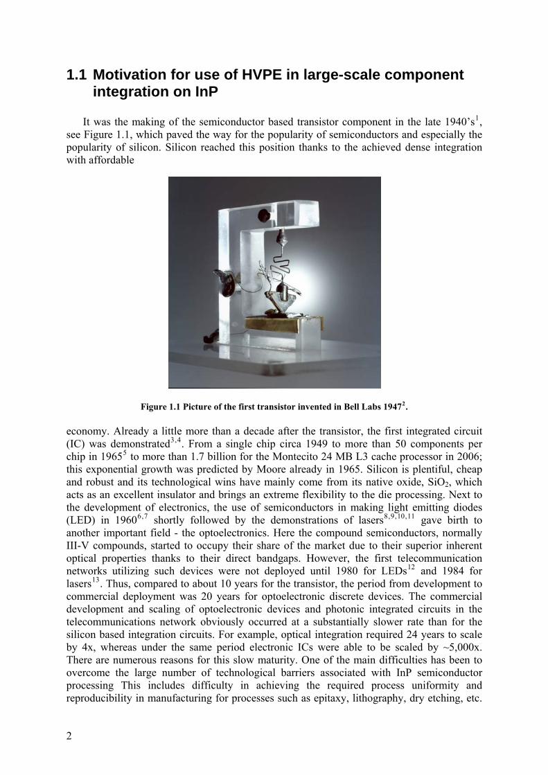
It was the making of the semiconductor based transistor component in the late 1940’s1,
see Figure 1.1, which paved the way for the popularity of semiconductors and especially the popularity of silicon. Silicon reached this position thanks to the achieved dense integration with affordable
Figure 1.1 Picture of the first transistor invented in Bell Labs 19472. economy. Already a little more than a decade after the transistor, the first integrated circuit (IC) was demonstrated3,4. From a single chip circa 1949 to more than 50 components per chip in 19655 to more than 1.7 billion for the Montecito 24 MB L3 cache processor in 2006; this exponential growth was predicted by Moore already in 1965. Silicon is plentiful, cheap and robust and its technological wins have mainly come from its native oxide, SiO2, which acts as an excellent insulator and brings an extreme flexibility to the die processing. Next to the development of electronics, the use of semiconductors in making light emitting diodes (LED) in 19606,7 shortly followed by the demonstrations of lasers8, , ,9 10 11 gave birth to another important field - the optoelectronics. Here the compound semiconductors, normally III-V compounds, started to occupy their share of the market due to their superior inherent optical properties thanks to their direct bandgaps. However, the first telecommunication networks utilizing such devices were not deployed until 1980 for LEDs12 and 1984 for lasers13. Thus, compared to about 10 years for the transistor, the period from development to commercial deployment was 20 years for optoelectronic discrete devices. The commercial development and scaling of optoelectronic devices and photonic integrated circuits in the telecommunications network obviously occurred at a substantially slower rate than for the silicon based integration circuits. For example, optical integration required 24 years to scale by 4x, whereas under the same period electronic ICs were able to be scaled by ~5,000x. There are numerous reasons for this slow maturity. One of the main difficulties has been to overcome the large number of technological barriers associated with InP semiconductor processing This includes difficulty in achieving the required process uniformity and reproducibility in manufacturing for processes such as epitaxy, lithography, dry etching, etc.
2
Additionally, it has proven very challenging from a design standpoint to monolithically integrate numerous devices and functions while keeping the process complexity low. All together, this has held back the successful manufacturing of III-V based complex multi-function integrated circuits.
After the introduction of lasers into the telecommunication systems, the commercial implementations focused on increasing higher data rates in discrete devices rather than on integration. It would take more than a decade before the first integrated device, the electroabsorption modulator-laser ( EML), consisting of two functions on a single chip, was first deployed in 1996 at 2.5 Gb/s and in 1998 at 10 Gb/s in long-haul terrestrial networks14. A few years later this was followed by the implementation of two additional functions (tuning and amplification), resulting in a transmitter consisting of a tunable EML with a semiconductor optical amplifier (SOA)15. However, although all of these small-scale photonic integrated circuits (PIC) meet the performance, cost and reliability requirements for deployment in the telecommunications network, their functionality remains limited with the relatively low level of integration (< 5 integrated functions/chip). Parallel to the development of devices and small-scale PICs, a steady development of processes and process equipments and quality of substrates has taken place. Driven by the improvements in III-V device and process technology as well as the ability for such devices to enable new network architectures a major inflection point in the PIC progression occurred recently when large-scale photonic integrated circuits using > 50 functions to provide a chip operating at an aggregate data rate of 100 Gb/s with performance and capability sufficient for commercial deployment was demonstrated by Infinera.
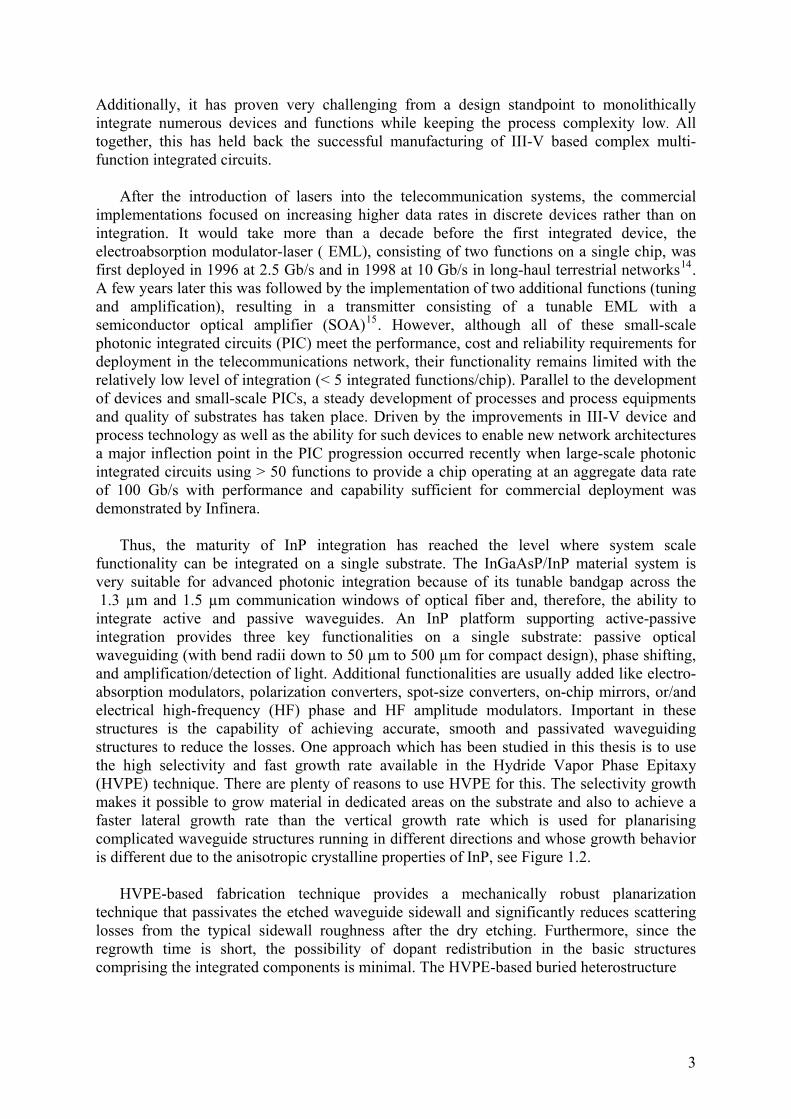
Thus, the maturity of InP integration has reached the level where system scale functionality can be integrated on a single substrate. The InGaAsP/InP material system is very suitable for advanced photonic integration because of its tunable bandgap across the 1.3 µm and 1.5 µm communication windows of optical fiber and, therefore, the ability to integrate active and passive waveguides. An InP platform supporting active-passive integration provides three key functionalities on a single substrate: passive optical waveguiding (with bend radii down to 50 µm to 500 µm for compact design), phase shifting, and amplification/detection of light. Additional functionalities are usually added like electro-absorption modulators, polarization converters, spot-size converters, on-chip mirrors, or/and electrical high-frequency (HF) phase and HF amplitude modulators. Important in these structures is the capability of achieving accurate, smooth and passivated waveguiding structures to reduce the losses. One approach which has been studied in this thesis is to use the high selectivity and fast growth rate available in the Hydride Vapor Phase Epitaxy (HVPE) technique. There are plenty of reasons to use HVPE for this. The selectivity growth makes it possible to grow material in dedicated areas on the substrate and also to achieve a faster lateral growth rate than the vertical growth rate which is used for planarising complicated waveguide structures running in different directions and whose growth behavior is different due to the anisotropic crystalline properties of InP, see Figure 1.2.
HVPE-based fabrication technique provides a mechanically robust planarization technique that passivates the etched waveguide sidewall and significantly reduces scattering losses from the typical sidewall roughness after the dry etching. Furthermore, since the regrowth time is short, the possibility of dopant redistribution in the basic structures comprising the integrated components is minimal. The HVPE-based buried heterostructure
3
Figure 1.2 (a) Schematic principle of an etched mesa structure. (b) Schematic picture of regrowth by layer by layer of mesa structures (c) Scanning electron microscopy (SEM) picture of InP regrowth of waveguides structures with different doping in grown layers which gives different contrast after stain-etching. (BH) waveguide fabrication technique has many advantages compared to conventional approaches used for realizing ridge, rib-loaded, or traditional buried curved waveguides. The HVPE-based fabrication technique requires one less regrowth step than the traditional BH fabrication process. In addition, the combined BH fabrication technique requires no critical control of the etch depth. This is necessary for a “shallow-etched” waveguide with the shallow-etching stopping at exactly 100 nm below the interface between the core and the upper cladding layers16.
Thus, one major intention has been to explore the use of HVPE and selective area growth in the fabrication for large-scale PIC chips for optical code-division multiple-access where the main challenge lies in the crystalline growth behavior for deeply etch waveguides whose directions are varied on top of the anisotropic InP substrate. An additional intention of this thesis is to exploit selective area growth.
1.2 Motivation for use of HVPE for realizing heteroepitaxy of InP on Si
1.2.1 Why InP on Silicon? Heteroepitaxy is necessary for the development of many new advanced devices and systems. Important fields include substrate engineering and device integration. Only a few semiconductor substrates are available in large area high-quality single crystals such as silicon and germanium. Silicon, the dominating substrate material in electronic industries, enjoys an advanced crystal manufacturing which makes it possible to fabricate 12 inch high-quality wafers almost free of defects at relatively low cost. Hence, large benefits can be derived from using silicon as templates for materials that either lack natural substrates or whose substrates are expensive and of much smaller sizes. Further, since no single material can simultaneously satisfy all the needs that are found in modern integrated circuits there is a large demand for integration of various functionalities on single chips. This would save the cost as it eliminates external inter-device connections and simplifies manufacturing processes such as device separation, assembly, burn-in tests and reliability.
4
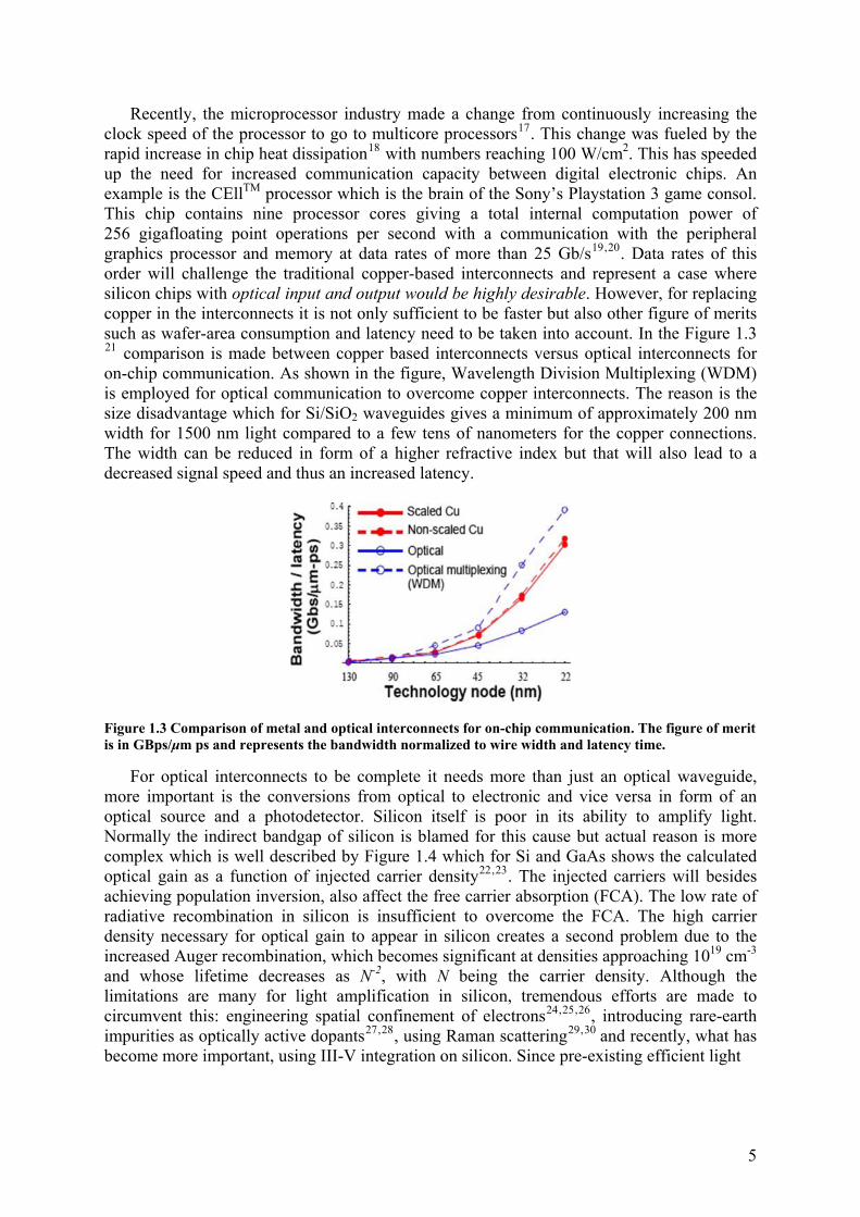
Recently, the microprocessor industry made a change from continuously increasing the clock speed of the processor to go to multicore processors17. This change was fueled by the rapid increase in chip heat dissipation18 with numbers reaching 100 W/cm2. This has speeded up the need for increased communication capacity between digital electronic chips. An example is the CEllTM processor which is the brain of the Sony’s Playstation 3 game consol. This chip contains nine processor cores giving a total internal computation power of 256 gigafloating point operations per second with a communication with the peripheral graphics processor and memory at data rates of more than 25 Gb/s19,20. Data rates of this order will challenge the traditional copper-based interconnects and represent a case where silicon chips with optical input and output would be highly desirable. However, for replacing copper in the interconnects it is not only sufficient to be faster but also other figure of merits such as wafer-area consumption and latency need to be taken into account. In the Figure 1.3 21 comparison is made between copper based interconnects versus optical interconnects for on-chip communication. As shown in the figure, Wavelength Division Multiplexing (WDM) is employed for optical communication to overcome copper interconnects. The reason is the size disadvantage which for Si/SiO2 waveguides gives a minimum of approximately 200 nm width for 1500 nm light compared to a few tens of nanometers for the copper connections. The width can be reduced in form of a higher refractive index but that will also lead to a decreased signal speed and thus an increased latency.
Figure 1.3 Comparison of metal and optical interconnects for on-chip communication. The figure of merit is in GBps/μm ps and represents the bandwidth normalized to wire width and latency time.
For optical interconnects to be complete it needs more than just an optical waveguide, more important is the conversions from optical to electronic and vice versa in form of an optical source and a photodetector. Silicon itself is poor in its ability to amplify light. Normally the indirect bandgap of silicon is blamed for this cause but actual reason is more complex which is well described by Figure 1.4 which for Si and GaAs shows the calculated optical gain as a function of injected carrier density22,23. The injected carriers will besides achieving population inversion, also affect the free carrier absorption (FCA). The low rate of radiative recombination in silicon is insufficient to overcome the FCA. The high carrier density necessary for optical gain to appear in silicon creates a second problem due to the increased Auger recombination, which becomes significant at densities approaching 1019 cm-3 and whose lifetime decreases as N-2, with N being the carrier density. Although the limitations are many for light amplification in silicon, tremendous efforts are made to circumvent this: engineering spatial confinement of electrons24, ,25 26, introducing rare-earth impurities as optically active dopants27,28, using Raman scattering29, 30 and recently, what has become more important, using III-V integration on silicon. Since pre-existing efficient light
5
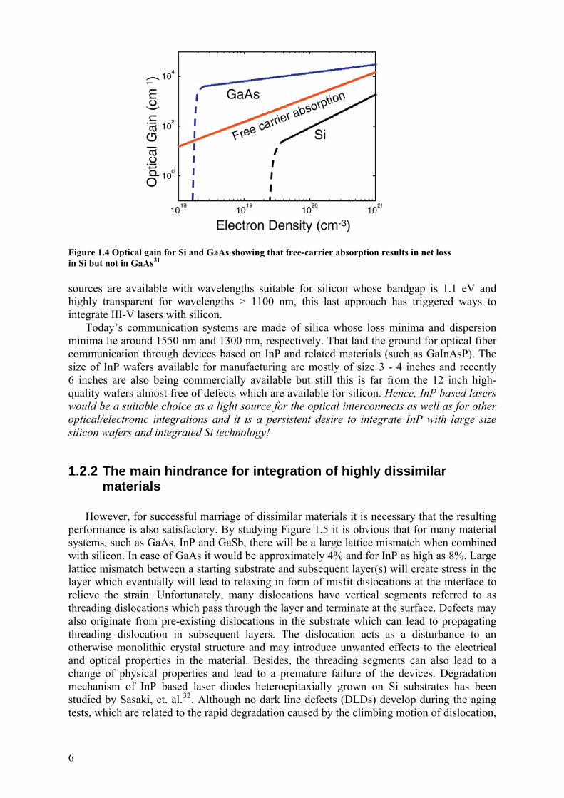
Figure 1.4 Optical gain for Si and GaAs showing that free-carrier absorption results in net loss in Si but not in GaAs31
sources are available with wavelengths suitable for silicon whose bandgap is 1.1 eV and highly transparent for wavelengths > 1100 nm, this last approach has triggered ways to integrate III-V lasers with silicon.
Today’s communication systems are made of silica whose loss minima and dispersion minima lie around 1550 nm and 1300 nm, respectively. That laid the ground for optical fiber communication through devices based on InP and related materials (such as GaInAsP). The size of InP wafers available for manufacturing are mostly of size 3 - 4 inches and recently 6 inches are also being commercially available but still this is far from the 12 inch high-quality wafers almost free of defects which are available for silicon. Hence, InP based lasers would be a suitable choice as a light source for the optical interconnects as well as for other optical/electronic integrations and it is a persistent desire to integrate InP with large size silicon wafers and integrated Si technology!
1.2.2 The main hindrance for integration of highly dissimilar materials
However, for successful marriage of dissimilar materials it is necessary that the resulting
performance is also satisfactory. By studying Figure 1.5 it is obvious that for many material systems, such as GaAs, InP and GaSb, there will be a large lattice mismatch when combined with silicon. In case of GaAs it would be approximately 4% and for InP as high as 8%. Large lattice mismatch between a starting substrate and subsequent layer(s) will create stress in the layer which eventually will lead to relaxing in form of misfit dislocations at the interface to relieve the strain. Unfortunately, many dislocations have vertical segments referred to as threading dislocations which pass through the layer and terminate at the surface. Defects may also originate from pre-existing dislocations in the substrate which can lead to propagating threading dislocation in subsequent layers. The dislocation acts as a disturbance to an otherwise monolithic crystal structure and may introduce unwanted effects to the electrical and optical properties in the material. Besides, the threading segments can also lead to a change of physical properties and lead to a premature failure of the devices. Degradation mechanism of InP based laser diodes heteroepitaxially grown on Si substrates has been studied by Sasaki, et. al.32. Although no dark line defects (DLDs) develop during the aging tests, which are related to the rapid degradation caused by the climbing motion of dislocation,
6
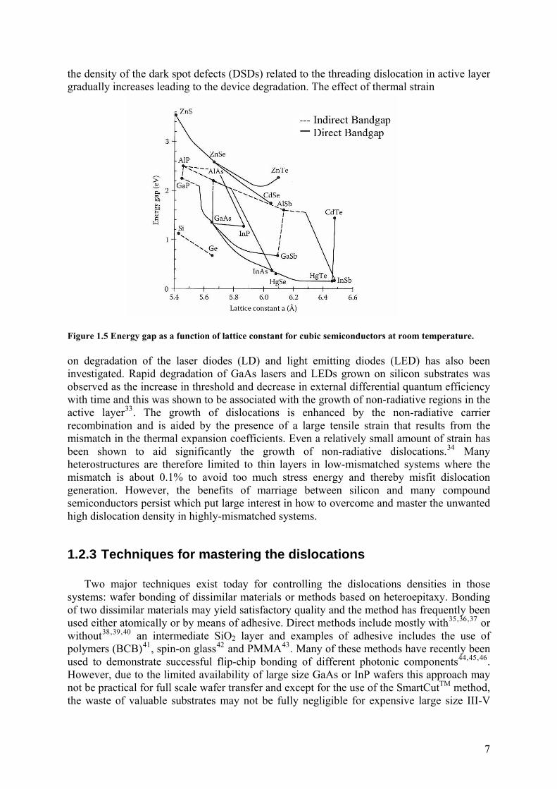
the density of the dark spot defects (DSDs) related to the threading dislocation in active layer
gradually increases leading to the device degradation. The effect of thermal strain
igure 1.5 Energy gap as a function of lattice constant for cubic semiconductors at room temperature.
n degradation of the laser diodes (LD) and light emitting diodes (LED) has also been
1.2.3 Techniques for mastering the dislocations
Two major techniques exist today for controlling the dislocations densities in those sys
F oinvestigated. Rapid degradation of GaAs lasers and LEDs grown on silicon substrates was observed as the increase in threshold and decrease in external differential quantum efficiency with time and this was shown to be associated with the growth of non-radiative regions in the active layer33. The growth of dislocations is enhanced by the non-radiative carrier recombination and is aided by the presence of a large tensile strain that results from the mismatch in the thermal expansion coefficients. Even a relatively small amount of strain has been shown to aid significantly the growth of non-radiative dislocations.34 Many heterostructures are therefore limited to thin layers in low-mismatched systems where the mismatch is about 0.1% to avoid too much stress energy and thereby misfit dislocation generation. However, the benefits of marriage between silicon and many compound semiconductors persist which put large interest in how to overcome and master the unwanted high dislocation density in highly-mismatched systems.
tems: wafer bonding of dissimilar materials or methods based on heteroepitaxy. Bonding of two dissimilar materials may yield satisfactory quality and the method has frequently been used either atomically or by means of adhesive. Direct methods include mostly with35, ,36 37 or without38, ,39 40 an intermediate SiO2 layer and examples of adhesive includes the use of polymers (BCB)41, spin-on glass42 and PMMA43. Many of these methods have recently been used to demonstrate successful flip-chip bonding of different photonic components44, ,45 46. However, due to the limited availability of large size GaAs or InP wafers this approach may not be practical for full scale wafer transfer and except for the use of the SmartCutTM method, the waste of valuable substrates may not be fully negligible for expensive large size III-V
7
wafers. Thermal strain due to the lattice mismatch is also of concern and efforts are made especially in the direct bonding methods to reduce the high annealing temperatures used47,48.
In heteroepitaxy there exist plenty of techniques for engineering the defects. Several methods have been applied to improve the material quality of InP grown on Si. Buffer layer approaches include growing a very thick layer, compositional grading and super lattice structures. Growing only a thick layer is often not adequate to be able to reduce the density of dislocations since that would need a layer thickness exceeding 100 µm which is not suitable for production of device quality material49. Graded layer method with a linearly or other compositional change has mainly been used for Si/SiGe and GaAsP/GaAs but has also been applied for low indium content on InGaP/GaP50. It has been successful to reduce the threading dislocation densities to 10-5 – 10-6 cm-2 when using practical growth rates and grading coefficients. But branch defects (characterized by meandering lines of strain contrasts) and surface roughening tend to impede the gliding of defects. The use of strained superlattice has been commonly used and has been shown to reduce the dislocation density of InP on Si51, ,52 53, but for being successful, the dislocation needs to glide all the way to a free sidewall which often means to the end of the substrate. Other methods involve growing on patterned Si substrates54,55, thermal annealing56,57 or using different intermediate layers between the silicon substrate and the InP such as GaAs58 or ZnSe59 or recently Gd2O3
60. All
of these methods have various constraints and difficulties, and some of them may not even be appropriate, but even the best results indicate defect densities above 10 cm . 5 -2
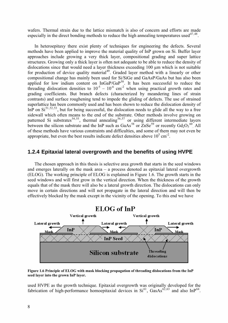
1.2.4 Epitaxial lateral overgrowth and the benefits of using HVPE
The chosen approach in this thesis is selective area growth that starts in the seed windows and emerges laterally on the mask area – a process denoted as epitaxial lateral overgrowth (ELOG). The working principle of ELOG is explained in Figure 1.6. The growth starts in the seed windows and will first grow in the vertical direction. When the thickness of the growth equals that of the mask there will also be a lateral growth direction. The dislocations can only move in certain directions and will not propagate in the lateral direction and will then be effectively blocked by the mask except in the vicinity of the opening. To this end we have
Figure 1.6 Principle of ELOG with mask blocking propagation of threading dislocations from the InP seed layer into the grown InP layer. used HVPE as the growth technique. Epitaxial overgrowth was originally developed for the fabrication of high-performance homoepitaxial devices in Si61, GasAs62,63 and also InP64.
8
The ability of ELOG to decrease the threading dislocation in heteroepitaxy structure of III-V on Si was first reported in 1980’s65 and later it has been applied for the growth of InP on Si66,67 and recent results indicate dislocation densities below 105 cm-2 68. For successful implementation ELOG requires a preferential growth with a higher growth rate in lateral direction than the vertical. This condition resembles the demands met in regrowth and the method is very suitable for HVPE due to its highly in-built selectivity. The HVPE advantage lies here in the ability to selectively grow only in the seed windows without deposition on the mask. The inherent strong selectivity gives a good control over the lateral and vertical growth rates and facilitates the necessity of keeping the lateral growth rate higher than the vertical for efficient defect filtering.
1.3 Major investigations of this thesis The major investigations done in this thesis are as follows: (i). Studying the application of HVPE for regrowth of semi-insulating InP:Fe to realize a
discrete and an integrated chip based on InP. The former is a multi-quantum well buried heterostructure laser emitting at 1.55 µm that makes use of AlGaInAs and InGaAsP as the barrier and well, respectively. Normally regrowth around Al containing materials are difficult. We undertake special etching precautions to fabricate a buried heterostructure laser of good performance. Concerning the integrated device, we demonstrate complex and densely packed buried arrayed waveguide (AWG) structures commonly encountered in advanced systems-on-the-chip for optical code-division multiple-access (O-CDMA). Selective epitaxial growth aspects specific to these complicated structures will be investigated. We also undertake mass transport studies on these AWGs.
(ii). Studies on and relevant to epitaxial lateral overgrowth (ELOG) of high quality InP on
silicon will be undertaken.
(iii). ELOG often encounters cases where most part of the surface is covered by mask. From the modeling on large mask area effects, their impact on the transport and kinetic properties will be established. Experimental verification will be done.
(iv). ELOG of InP on silicon-on-insulators will also be experimented. This is particularly interesting for integrating silicon/silicon dioxide waveguides with InP.
(v). It is known that ELOG causes strain in the materials. We will undertake the effect of strain in the ELOG structures by synchrotron X-ray measurements.
(vi). We will undertake modeling to reduce the propagation of threading dislocation from the seed layer into the ELOG layer through the openings. Experiments will be conducted to verify the simulation. Towards achieving this goal, we will reduce the openings size down to ~100 nm to conduct ELOG contrary to the conventional openings size in the ranges of micrometers. We call this technique nano-ELOG.
(vii). We also will study a novel net pattern design to conduct nano-ELOG. Several characterization techniques will be employed to assess the quality of ELOG grown InP.
9

The structure of the thesis is as follows. In chapter 2, some background information on the crystallographic structure of III-V compound semiconductors, comparison of several growth techniques for ELOG, defect structures encountered in ELOG InP on InP/Si growth, and characterization techniques for heterostructures will be described. Chapter 3 will summarize and discuss the major results. A summary of the papers will be presented in chapter 4 and, finally, chapter 5 will contain a summary, conclusion and suggestions for future work.
10
2 Background
This section contains an overview on different fields related to and encountered in this thesis. The main focus of this chapter is on the zinc blende crystal structure and various types of defects and dislocations. Hydride vapor phase epitaxy, the growth method employed in this thesis is also introduced. Several characterization methods utilized in this thesis as well as a short overview of the application areas of lasers and arrayed waveguide gratings are also described. The main intention of this chapter is to give more of an introduction to the subjects rather than to give a complete and detailed survey; the choice of topics of relevance and depth of treatment of course have certain correlation to the interest of the author. 2.1 III-V semiconductor materials
For optoelectronic applications, the quantum efficiency in emitting and detecting light is a major requirement. Elemental semiconductors from the IV column such as Si, Ge and their alloys, Si1-xGex, are not appropriate materials for optoelectronic devices. On the other hand, several compound semiconductors and their alloys offer many of the desired properties for optoelectronics purposes and can be synthesized without much difficulty. Compound semiconductors are made from elements of different columns of the periodic table, for example, III-V and II-IV compounds. Among all of them, III-V compound semiconductors are the most widely used. In addition, ternary or quaternary semiconductor alloys made of group III and group V atoms can be realized. By modifying the atomic composition of these alloys, it is possible to obtain different bandgaps and, therefore, varying emission wavelengths for light sources.
2.2 Crystallographic properties
Semiconductors in common use are nearly always single-crystal materials. A crystal is a periodic arrangement of atoms in space. A space lattice and a basis comprise a crystal structure. The periodic arrangement of points on which atoms or groups of atoms can be placed is described by the space lattice whereas the basis may consist of a single atom or an arrangement of atoms placed at each lattice point. There are 14 space lattices, called the Bravais lattices69, of these the face-centered cubic (FCC) lattice is the most relevant in this thesis.
11
2.2.1 Diamond lattice
Common semiconductors such as Si, Ge and Si-Ge alloys all crystallize in the diamond structure. The diamond structure belongs to FCC lattice with a basis of two atoms at each lattice point, one at (0, 0, 0) and the other at (a/4, a/4, a/4), where a is the lattice constant. The structure can be thought of as two FCC lattices where one lattice is displaced from the other by one quarter of the unit cell diagonal. The space group is ( )73 hOmFd . The lattice constant, a, is equal to the length of the cubic unit cell. The atoms in the diamond lattice are tetrahedrally bonded and each atom is covalently bonded to its four nearest neighbors.
2.2.2 Zinc blende lattice
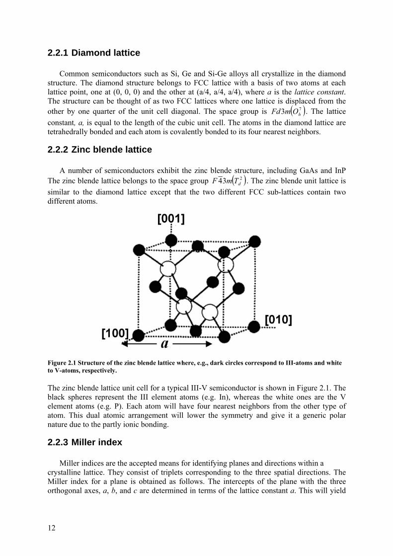
A number of semiconductors exhibit the zinc blende structure, including GaAs and InP The zinc blende lattice belongs to the space group ( )234 dTmF . The zinc blende unit lattice is similar to the diamond lattice except that the two different FCC sub-lattices contain two different atoms.
Figure 2.1 Structure of the zinc blende lattice where, e.g., dark circles correspond to III-atoms and white to V-atoms, respectively. The zinc blende lattice unit cell for a typical III-V semiconductor is shown in Figure 2.1. The black spheres represent the III element atoms (e.g. In), whereas the white ones are the V element atoms (e.g. P). Each atom will have four nearest neighbors from the other type of atom. This dual atomic arrangement will lower the symmetry and give it a generic polar nature due to the partly ionic bonding.
2.2.3 Miller index
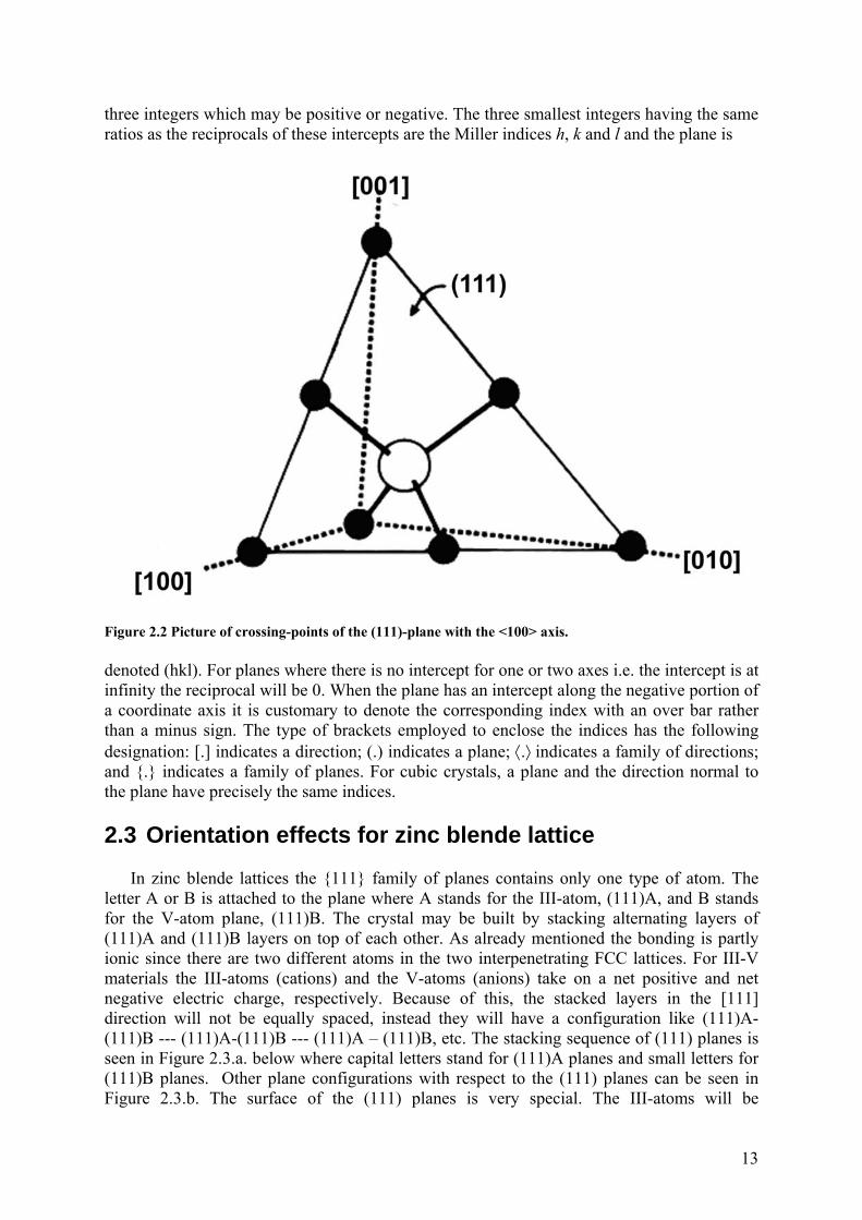
Miller indices are the accepted means for identifying planes and directions within a crystalline lattice. They consist of triplets corresponding to the three spatial directions. The Miller index for a plane is obtained as follows. The intercepts of the plane with the three orthogonal axes, a, b, and c are determined in terms of the lattice constant a. This will yield
12
three integers which may be positive or negative. The three smallest integers having the same ratios as the reciprocals of these intercepts are the Miller indices h, k and l and the plane is
Figure 2.2 Picture of crossing-points of the (111)-plane with the <100> axis. denoted (hkl). For planes where there is no intercept for one or two axes i.e. the intercept is at infinity the reciprocal will be 0. When the plane has an intercept along the negative portion of a coordinate axis it is customary to denote the corresponding index with an over bar rather than a minus sign. The type of brackets employed to enclose the indices has the following designation: [.] indicates a direction; (.) indicates a plane; ⟨.⟩ indicates a family of directions; and {.} indicates a family of planes. For cubic crystals, a plane and the direction normal to the plane have precisely the same indices. 2.3 Orientation effects for zinc blende lattice
In zinc blende lattices the {111} family of planes contains only one type of atom. The letter A or B is attached to the plane where A stands for the III-atom, (111)A, and B stands for the V-atom plane, (111)B. The crystal may be built by stacking alternating layers of (111)A and (111)B layers on top of each other. As already mentioned the bonding is partly ionic since there are two different atoms in the two interpenetrating FCC lattices. For III-V materials the III-atoms (cations) and the V-atoms (anions) take on a net positive and net negative electric charge, respectively. Because of this, the stacked layers in the [111] direction will not be equally spaced, instead they will have a configuration like (111)A-(111)B --- (111)A-(111)B --- (111)A – (111)B, etc. The stacking sequence of (111) planes is seen in Figure 2.3.a. below where capital letters stand for (111)A planes and small letters for (111)B planes. Other plane configurations with respect to the (111) planes can be seen in Figure 2.3.b. The surface of the (111) planes is very special. The III-atoms will be
13
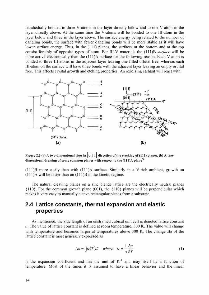
tetrahedrally bonded to three V-atoms in the layer directly below and to one V-atom in the layer directly above. At the same time the V-atoms will be bonded to one III-atom in the layer below and three in the layer above. The surface energy being related to the number of dangling bonds, the surface with fewer dangling bonds will be more stable as it will have lower surface energy. Thus, in the (111) planes, the surfaces at the bottom and at the top consist forcibly of opposite types of atom. For III-V materials the (111)B surface will be more active electronically than the (111)A surface for the following reason. Each V-atom is bonded to three III-atoms in the adjacent layer leaving one filled orbital free, whereas each III-atom on the surface will have three bonds with the adjacent layer leaving an empty orbital free. This affects crystal growth and etching properties. An oxidizing etchant will react with
Figure 2.3 (a) A two-dimensional view in [ ]110 direction of the stacking of (111) planes. (b) A two-dimensional drawing of some common planes with respect to the (111)A plane70
(111)B more easily than with (111)A surface. Similarly in a V-rich ambient, growth on (111)A will be faster than on (111)B in the kinetic regime.
The natural cleaving planes on a zinc blende lattice are the electrically neutral planes {110}. For the common growth plane (001), the {110} planes will be perpendicular which makes it very easy to manually cleave rectangular pieces from a substrate. 2.4 Lattice constants, thermal expansion and elastic
properties
As mentioned, the side length of an unstrained cubical unit cell is denoted lattice constant a. The value of lattice constant is defined at room temperature, 300 K. The value will change with temperature and becomes larger at temperatures above 300 K. The change Δa of the lattice constant is most generally expressed as ( )∫ ∂
∂==Δ
Ta
awheredtTa 1αα (1)
is the expansion coefficient and has the unit of K-1 and may itself be a function of temperature. Most of the times it is assumed to have a linear behavior and the linear
14

expansion value at 300 K is used. For materials such as InP there is a lack of data for an accurate temperature dependence of the expansion coefficient.
Lattice mismatch and thermal expansion can lead to strain in the semiconductor which in turn may affect several properties of the material. The change of position of a point in a strained material compared with its position in an unstrained state is given by the displacement vector u = [ux, uy, uz]. By definition, in linear elasticity and when |∂ui/∂uj| << 1 for i,j = 1, 2, 3* then the nine different strain components are given by the first derivates of the components of the displacement vector and are:
xu
e xxx ∂
∂= ,
yu
e yyy ∂
∂= ,
zue z
zz ∂∂
= (2)
⎟⎟⎠
⎞⎜⎜⎝
⎛∂
∂+
∂∂
==x
uy
uee yx
yxxy 21 (3a)
⎟⎠⎞
⎜⎝⎛
∂∂
+∂
∂==
xu
zu
ee zxzxxz 2
1 (3b)
⎟⎟⎠
⎞⎜⎜⎝
⎛∂
∂+
∂
∂==
yu
zu
ee zyzyyz 2
1 (3c)
Here the first three terms (eq. (2)) are the normal strains and represents the fractional change in length elements parallel to the x, y and z axes. The other six components (eqs. 3a-3c) are the shear strain and have a simple physical meaning indicated by Figure 2.4.
Figure 2.4 (a) Pure shear strain and (b) simple shear strain of an area element in the xy plane71
* This last approximation is also referred to as engineering strain or small strain or infinitesimal strain and is valid when the deformations are small.
15
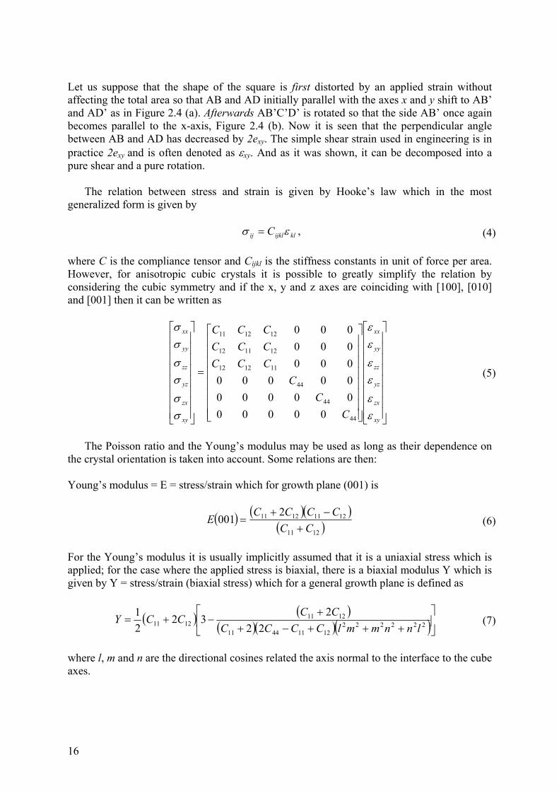
Let us suppose that the shape of the square is first distorted by an applied strain without affecting the total area so that AB and AD initially parallel with the axes x and y shift to AB’ and AD’ as in Figure 2.4 (a). Afterwards AB’C’D’ is rotated so that the side AB’ once again becomes parallel to the x-axis, Figure 2.4 (b). Now it is seen that the perpendicular angle between AB and AD has decreased by 2exy. The simple shear strain used in engineering is in practice 2exy and is often denoted as εxy. And as it was shown, it can be decomposed into a pure shear and a pure rotation.
The relation between stress and strain is given by Hooke’s law which in the most generalized form is given by klijklij C εσ = , (4) where C is the compliance tensor and Cijkl is the stiffness constants in unit of force per area. However, for anisotropic cubic crystals it is possible to greatly simplify the relation by considering the cubic symmetry and if the x, y and z axes are coinciding with [100], [010] and [001] then it can be written as
⎥⎥⎥⎥⎥⎥⎥⎥
⎦
⎤
⎢⎢⎢⎢⎢⎢⎢⎢
⎣
⎡
⎥⎥⎥⎥⎥⎥⎥⎥
⎦
⎤
⎢⎢⎢⎢⎢⎢⎢⎢
⎣
⎡
=
⎥⎥⎥⎥⎥⎥⎥⎥
⎦
⎤
⎢⎢⎢⎢⎢⎢⎢⎢
⎣
⎡
xy
zx
yz
zz
yy
xx
xy
zx
yz
zz
yy
xx
CC
CCCCCCCCCC
εε
εε
εε
σσ
σσ
σσ
44
44
44
111212
121112
121211
000000000000000000000000
(5)
The Poisson ratio and the Young’s modulus may be used as long as their dependence on
the crystal orientation is taken into account. Some relations are then: Young’s modulus = E = stress/strain which for growth plane (001) is ( ) ( )( )
( )1211
12111211 2001CC
CCCCE+
−+= (6)
For the Young’s modulus it is usually implicitly assumed that it is a uniaxial stress which is applied; for the case where the applied stress is biaxial, there is a biaxial modulus Y which is given by Y = stress/strain (biaxial stress) which for a general growth plane is defined as
( ) ( )( )( )( )⎥⎦
⎤⎢⎣
⎡+++−+
+−+= 222222
12114411
12111211 22
23221
lnnmmlCCCCCCCCY (7)
where l, m and n are the directional cosines related the axis normal to the interface to the cube axes.
16

For the growth on (001) it takes the simple expression
( )11
212
12112001CCCCY −+= (8)
The shear modulus G is defined as the ratio of shear stress to shear strain which for (001) plane is:
21211 CCG −
= (9)
Finally the Poisson ratio ν is defined as the transverse contraction to the longitudinal extension for a uniaxial stress in the longitudinal direction which for growth plane (001) is ( )
1211
12001CC
C+
=ν (10)
2.4.1 Resolved shear stress
The resolved shear stress is denoted by τ and is the stress resolved in a particular direction in a glide plane and is often involved in heteroepitaxy. The stress is defined as σ = F/A and from Figure 2.5 it follows that the inclined surface has an area equal to A/cos ø and
Figure 2.5 Resolved force in the direction with angle λ from the force direction at an inclined slip plane surface with angle φ between the force direction and the slip plane normal. the force F has a component Fcos λ in a particular direction which gives a resolved stress in the direction λ in the plane ø equal to
λφτ coscosAF
= (11)
17
2.5 Epitaxial growth techniques for III-V materials
Four commonly used growth techniques for semiconductor materials are Liquid Phase Epitaxy (LPE), Vapor Phase Epitaxy (VPE), Molecular Beam Epitaxy (MBE) and Metal-Organic Vapor Phase Epitaxy (MOVPE). Among these there exist additional more or less commonly practiced subtypes. The two first growth methods are so-called near thermodynamic equilibrium techniques whereas the two last ones are far-off equilibrium. Shaw has exemplified that a solid heterogeneous reaction can be limited basically by one of the three steps: 1) input mass transport, 2) mass transport due to diffusion and 3) surface kinetics72. In LPE and VPE it is usually step (1) which limits the growth, in MOVPE step (2) and in MBE step (3). Step (1) is typical for a process operating close to equilibrium. This feature of the VPE process arises from the reversible process occurring at the interface due to the volatility of the chlorides of group III species at the operating temperatures and where the shift from the equilibrium mainly depends on the decomposition of the hydrides transporting the V-species. The benefits of a near-equilibrium growth process are:
• Growth rates are in principle determined by the mass input reactants and very high growth rates (> 20 µm/h) can easily be achieved. This is because; being a near equilibrium process, a small change in chemical potential between the gases and the solid affects the growth rate considerably.
• The volatility of group III chlorides renders their absorption on the dielectric mask with respect to the semiconductor surface difficult. This inherent property of VPE makes it an excellent technique for selective growth where certain areas are protected by dielectric masks to hinder the growth in those areas.
• In the kinetically controlled regime (at low operating temperature) the growth rates are different at different crystal planes but will coincide at high temperatures in the thermodynamically controlled regime. At normal conditions, for growth on non-planar substrates there will be a natural driving force to reach stable crystallographic directions. Since (001) substrates are similar to {hhl} planes the resulting effect will lead to a planarization.
The main drawback is the difficulty in growing very abrupt interfaces caused by the reversible process and the slow switching between the vent and run. This makes it hard to grow very thin layers with abrupt interfaces, such as quantum wells. Since it is a hot-wall reactor there is a risk for extraneous deposition on the reactor wall.
2.6 Hydride Vapor Phase Epitaxy (HVPE)
HVPE together with Chloride VPE (Cl-VPE) are two variations of VPE. These are both similar in the way they work and the final reaction in both techniques can be described by )(2)(2)()()(2 22 gHClcInPgHgPgInCl +=++ (12) Since the vapor pressure of InCl is very small the gas needs to be generated in situ through the reaction between Cl and molten In. In Cl-VPE the precursor PCl3 acts both as a reactant for generating InCl and is also the precursor for P. In HVPE this process is separated where
18
HCl is used to generate InCl whereas the precursor for P is PH3. Accordingly, for HVPE the reactions that make up (12) are
)()(2)(2)(2 2 gHgInClgHCllIn +=+ (13) )(3)()(2 223 gHgPgPH += . (14)
At low pressures the number of collisions between PH3 molecules is relatively small and the decomposition becomes limited making the growth reaction involving PH3 molecules instead of P2 or P4. In general, the construction of the quartz container holding the molten III-metal is made so that the reaction (13) is close to 100% in efficiency and it is common to assume the same flow of InCl as the inlet flow of HCl. The reaction at low pressure is then commonly written as 23 )( HHClsInPPHInCl ++⇔+ . (15) The reaction rate constant at the equilibrium is determined by the ratio of the partial pressures [ ] [ ]
[ ] [ ]EqEq
EqEqT PHInCl
HHClK
3
2= . (16)
γ, the relative gas phase supersaturation of the reaction can be defined as the state of advancement of the growth reaction with respect to equilibrium and is expressed as [ ][ ]
[ ][ ] 12
3 −= TKHHClPHInCl
γ . (17)
The deposition of InP can either take place as a two-dimensional nucleation73 or as a Burton-Cabrera-Frank (BCF) spiral growth74. In the case of an existing perfect surface, i.e. dislocation free, the mechanism of a 2D growth mode applies. In order to adsorb the first nuclei on the surface from where additional species will attach to form a continuous one-atomic high layer there is a demand on a lowest critical supersaturation. Above this lowest level the growth rate will increase exponentially with supersaturation as
⎟⎟⎠
⎞⎜⎜⎝
⎛−∝ 2
12 exp
TCGr D γ
, (18)
where Gr2D is the 2D growth rate, T is the temperature and C1 is a constant. However, for surfaces containing a high density of dislocations, the surface steps where the adatoms attach will be provided by the emerging points of the dislocations having their Burgers vector normal to the surface. For the general case with groups of dislocations the growth rate will be given by
⎟⎟⎠
⎞⎜⎜⎝
⎛⎟⎟⎠
⎞⎜⎜⎝
⎛=
γγ
γγε 1
1
2
tanhCGrBCF , (19)
where C and γ1 are constants and ε is the dislocation density. For low supersaturation (γ < γ1) GrBCF will be approximated by Cε(γ2 /γ1) and for high supersaturation (γ > γ1) by Cγ.
19
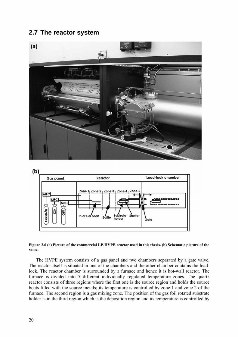
2.7 The reactor system
Figure 2.6 (a) Picture of the commercial LP-HVPE reactor used in this thesis. (b) Schematic picture of the same.
The HVPE system consists of a gas panel and two chambers separated by a gate valve. The reactor itself is situated in one of the chambers and the other chamber contains the load-lock. The reactor chamber is surrounded by a furnace and hence it is hot-wall reactor. The furnace is divided into 5 different individually regulated temperature zones. The quartz reactor consists of three regions where the first one is the source region and holds the source boats filled with the source metals; its temperature is controlled by zone 1 and zone 2 of the furnace. The second region is a gas mixing zone. The position of the gas foil rotated substrate holder is in the third region which is the deposition region and its temperature is controlled by
20
zone 4. Zone 3 and zone 5 of the furnace act as temperature gradient controllers. The samples are transported mechanically between the two chambers.
The load-lock chamber can hold a stabilization flow of V-hydrides making it possible to cool down the samples fast instead of keeping them in the slow-cooling reactor chamber. The load-lock chamber can be isolated from the reactor by the gate valve and hence it can be purged and pumped separately.
The main sources in the gas panel constitute of HCl, V-hydrides, such as phosphine (PH3), carrier gases (H2 and/or N2) and doping sources such as ferrocene (Fe(C5H5)2) and hydrogen sulphide (H2S). 2.8 Dopants in HVPE
The source for n-type doping is H2S. The S atom will replace the P atom and act as a donor. Due to the polar property of the zinc blende lattice there is an inhomogeneous incorporation efficiency for different growth planes. Several studies have been performed on the incorporation of S, as well as other dopants, for different crystallographic directions75, ,76 77. The incorporation efficiency for n-type dopants was found to follow (111)A > (001) > (111)B. For p-dopants the reverse is true. The effect of S-dopant on dislocation density in ELOG grown InP/Si has been studied. Sulphur has been found to improve the morphology and reduce the dislocation density, probably by inhibiting the threading dislocation movement from the InP seed layer78.
Semi-insulating (SI) semiconductors play a major role in device applications because they exhibit close to the intrinsic carrier density permissible for a given bandgap and are valued for their high resistivity and short carrier lifetimes. They provide device isolation for integrated circuits and current blocking layers for heterostructure lasers. The presence of crystal defects, surfaces, or dopant atoms lead to the appearance of energy levels within the bandgap of a semiconductor. These levels are called shallow if they are near a band edge and deep if they are far (>>kT at 300 K) from the band edges. At room temperature (RT), shallow impurities are mostly ionised since there is enough thermal energy to make carriers at shallow donor (acceptor) levels jump over the small energy gap into the conduction (valence) band. In contrast, due to their energy position near the middle of the bandgap, such transition is less probable with the deep centres (impurities or defects) at RT. However, deep centres may become ionised by trapping free electrons (holes) from the conduction (valence) band. Deep centres can be classified according to their charge state. Centres with a neutral and negatively charged state are called acceptor-like states, whereas centres with a neutral and positively charged state are called donor-like states. Thus, acceptor-like (donorlike) deep centres are neutral in p-type (n-type) semiconductors and ionised in n-type (p-type) semiconductors79. The semi-insulating character of the semiconductors is formed when a dominant deep level cancels (compensates) the net charges from other defect and dopant levels. In this way, the free carrier concentration is reduced and the Fermi level is pinned at an energy near the dominant deep level, which can be located anywhere within the band structure. Therefore, in general, a deep level close to the middle of the bandgap is preferred in order to obtain high resistivity.
21
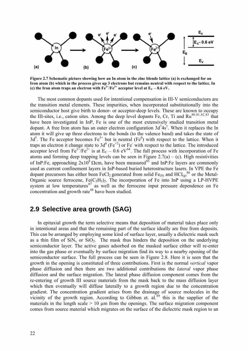
Figure 2.7 Schematic picture showing how an In atom in the zinc blende lattice (a) is exchanged for an Iron atom (b) which in the process gives up 3 electrons but remains neutral with respect to the lattice. In (c) the Iron atom traps an electron with Fe3+/Fe2+ acceptor level at EC – 0.6 eV.
The most common dopants used for intentional compensation in III-V semiconductors are the transition metal elements. These impurities, when incorporated substitutionally into the semiconductor host give birth to donor- or acceptor-deep levels. These are known to occupy the III-sites, i.e., cation sites. Among the deep level dopants Fe, Cr, Ti and Ru80, , ,81 82 83 that have been investigated in InP, Fe is one of the most extensively studied transition metal dopant. A free Iron atom has an outer electron configuration 3d74s1. When it replaces the In atom it will give up three electrons to the bonds (to the valence band) and takes the state of 3d5. The Fe acceptor becomes Fe3+ but is neutral (Fe0) with respect to the lattice. When it traps an electron it change state to 3d6 (Fe+2) or Fe- with respect to the lattice. The introduced acceptor level from Fe3+/Fe2+ is at EC – 0.6 eV84. The full process with incorporation of Fe atoms and forming deep trapping levels can be seen in Figure 2.7(a) – (c). High resistivities of InP:Fe, approaching 2x10⁸
Ωcm, have been measured85 and InP:Fe layers are commonly used as current confinement layers in InP-based buried heterostructure lasers. In VPE the Fe dopant precursors has either been FeCl2 generated from solid Fe(S) and HCl(g)
86 or the Metal-Organic source ferrocene, Fe(C5 5 2H ) . The incorporation of Fe into InP using a LP-HVPE system at low temperatures87 as well as the ferrocene input pressure dependence on Fe concentration and growth rate have been studied. 88
2.9 Selective area growth (SAG)
In epitaxial growth the term selective means that deposition of material takes place only in intentional areas and that the remaining part of the surface ideally are free from deposits. This can be arranged by employing some kind of surface layer, usually a dielectric mask such as a thin film of SiNx or SiO2. The mask thus hinders the deposition on the underlying semiconductor layer. The active gases adsorbed on the masked surface either will re-enter into the gas phase or eventually by surface migration find its way to a nearby opening of the semiconductor surface. The full process can be seen in Figure 2.8. Here it is seen that the growth in the opening is constituted of three contributions. First is the normal vertical vapor phase diffusion and then there are two additional contributions the lateral vapor phase diffusion and the surface migration. The lateral phase diffusion component comes from the re-entering of growth III source materials from the mask back to the mass diffusion layer which then eventually will diffuse laterally to a growth region due to the concentration gradient. The concentration gradient arises from the drainage of source molecules in the vicinity of the growth region. According to Gibbon et. al.89 this is the supplier of the materials in the length scale > 10 µm from the openings. The surface migration component comes from source material which migrates on the surface of the dielectric mask region to an
22
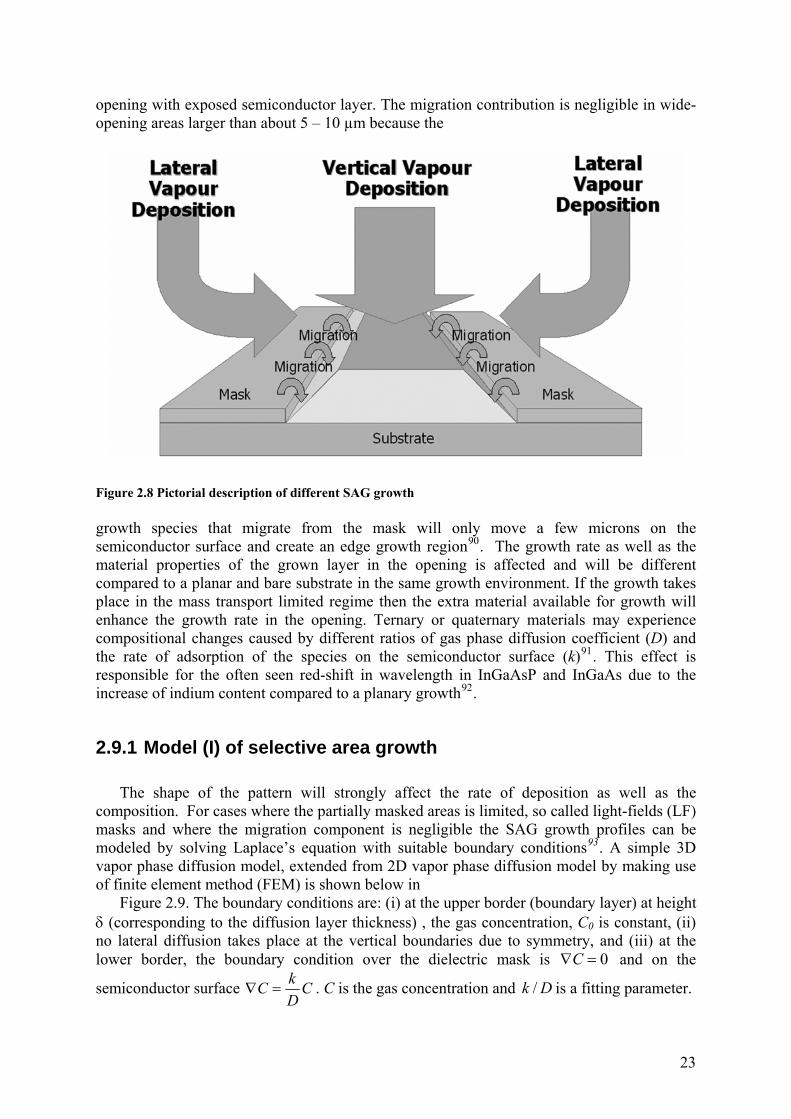
opening with exposed semiconductor layer. The migration contribution is negligible in wide-opening areas larger than about 5 – 10 µm because the
Figure 2.8 Pictorial description of different SAG growth growth species that migrate from the mask will only move a few microns on the semiconductor surface and create an edge growth region90. The growth rate as well as the material properties of the grown layer in the opening is affected and will be different compared to a planar and bare substrate in the same growth environment. If the growth takes place in the mass transport limited regime then the extra material available for growth will enhance the growth rate in the opening. Ternary or quaternary materials may experience compositional changes caused by different ratios of gas phase diffusion coefficient (D) and the rate of adsorption of the species on the semiconductor surface (k)91. This effect is responsible for the often seen red-shift in wavelength in InGaAsP and InGaAs due to the increase of indium content compared to a planary growth92.
2.9.1 Model (I) of selective area growth
The shape of the pattern will strongly affect the rate of deposition as well as the composition. For cases where the partially masked areas is limited, so called light-fields (LF) masks and where the migration component is negligible the SAG growth profiles can be modeled by solving Laplace’s equation with suitable boundary conditions93. A simple 3D vapor phase diffusion model, extended from 2D vapor phase diffusion model by making use of finite element method (FEM) is shown below in
Figure 2.9. The boundary conditions are: (i) at the upper border (boundary layer) at height δ (corresponding to the diffusion layer thickness) , the gas concentration, C0 is constant, (ii) no lateral diffusion takes place at the vertical boundaries due to symmetry, and (iii) at the lower border, the boundary condition over the dielectric mask is and on the
semiconductor surface
0=∇C
CDkC =∇ . C is the gas concentration and is a fitting parameter. Dk /
23
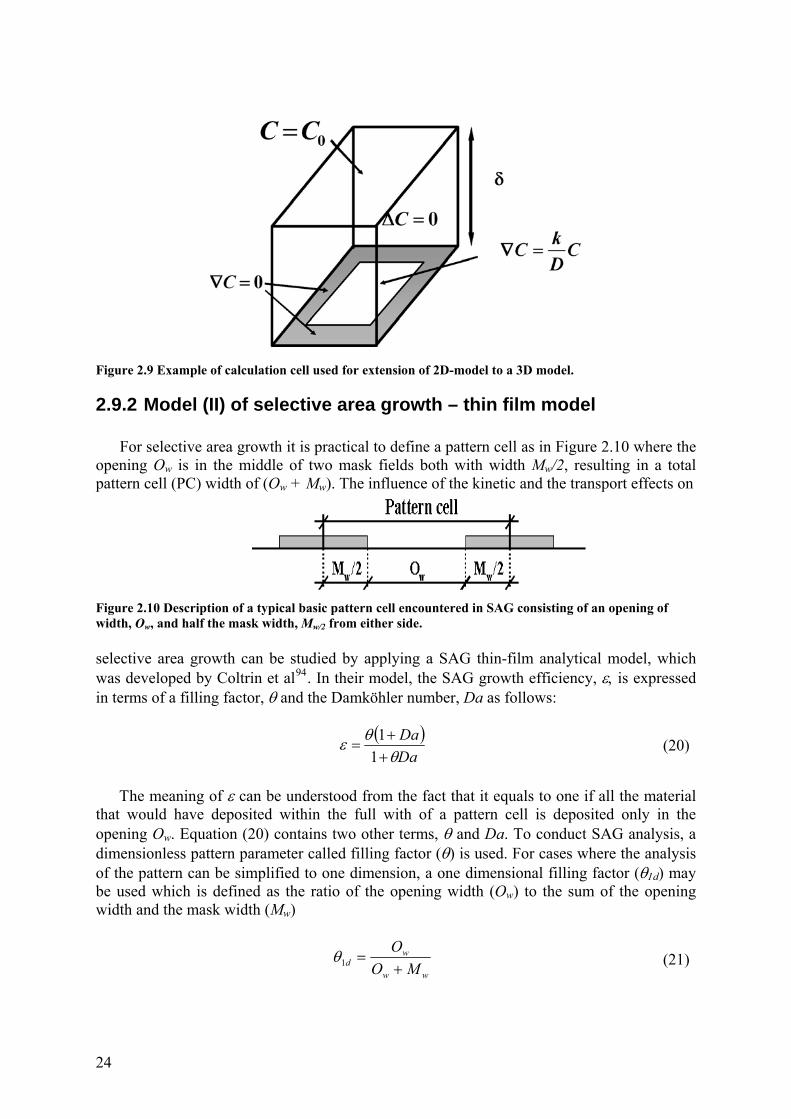
Figure 2.9 Example of calculation cell used for extension of 2D-model to a 3D model.
2.9.2 Model (II) of selective area growth – thin film model
For selective area growth it is practical to define a pattern cell as in Figure 2.10 where the opening Ow is in the middle of two mask fields both with width Mw/2, resulting in a total pattern cell (PC) width of (Ow + Mw). The influence of the kinetic and the transport effects on
Figure 2.10 Description of a typical basic pattern cell encountered in SAG consisting of an opening of width, Ow, and half the mask width, Mw/2 from either side. selective area growth can be studied by applying a SAG thin-film analytical model, which was developed by Coltrin et al94. In their model, the SAG growth efficiency, ε, is expressed in terms of a filling factor, θ and the Damköhler number, Da as follows: ( )
DaDa
θθε
++
=11 (20)
Τhe meaning of ε can be understood from the fact that it equals to one if all the material
that would have deposited within the full with of a pattern cell is deposited only in the opening Ow. Equation (20) contains two other terms, θ and Da. To conduct SAG analysis, a dimensionless pattern parameter called filling factor (θ) is used. For cases where the analysis of the pattern can be simplified to one dimension, a one dimensional filling factor (θ1d) may be used which is defined as the ratio of the opening width (Ow) to the sum of the opening width and the mask width (Mw)
ww
wd MO
O+
=1θ (21)
24
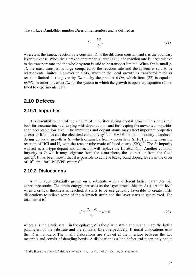
The surface Damköhler number Da is dimensionless and is defined as
DkDa δ
= , (22)
where k is the kinetic reaction rate constant , D is the diffusion constant and δ is the boundary layer thickness. When the Damköhler number is large (>>1), the reaction rate is large relative to the transport rate and the whole system is said to be transport limited. When Da is small (≤ 1), the mass transport is large compared to the reaction rate and the system is said to be reaction-rate limited. However in SAG, whether the local growth is transport-limited or reaction-limited is not given by Da but by the product θ Da, which from (22) is equal to θkδ/D. In order to extract Da for the system in which the growth is operated, equation (20) is fitted to experimental data.
2.10 Defects
2.10.1 Impurities
It is essential to control the amount of impurities during crystal growth. This holds true both for accurate intential doping with dopant atoms and for keeping the unwanted impurities at an acceptable low level. The impurities and dopant atoms may affect important properties as carrier lifetimes and the electrical conductivity95. In HVPE the main impurity introduced during epitaxial growth is Si which originates from chlorosilane SiH3Cl coming from the reaction of HCl and H2 with the reactor tube made of fused quartz (SiO2)96 The Si impurity will act as a n-type dopant and as such it will replace the III atom (In). Another common impurity is O which may originate from the atmosphere, the sources or from the fused quartz2. It has been shown that it is possible to achieve background doping levels in the order of 1014 cm-3 for LP-HVPE systems97.
2.10.2 Dislocations
A thin layer epitaxially grown on a substrate with a different lattice parameter will experience strain. The strain energy increases as the layer grows thicker. At a certain level when a critical thickness is reached, it starts to be energetically favorable to create misfit dislocations to relieve some of the mismatch strain and the layer starts to get relaxed. The total misfit is*
δε +=−
=l
ls
aaa
f (23)
where ε is the elastic strain in the epilayer, δ is the plastic strain and as and al are the lattice parameters of the substrate and the epitaxial layer, respectively. If misfit dislocations exist then δ is non-zero. The misfit dislocations are situated at the interface between the two materials and consist of dangling bonds. A dislocation is a line defect and it can only end at
* In the literature other definitions such as f =( as – al)/as and f = (as – al)/al. also exist
25
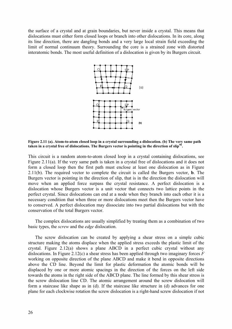
the surface of a crystal and at grain boundaries, but never inside a crystal. This means that dislocations must either form closed loops or branch into other dislocations. In its core, along its line direction, there are dangling bonds and a very large local strain field exceeding the limit of normal continuum theory. Surrounding the core is a strained zone with distorted interatomic bonds. The most useful definition of a dislocation is given by its Burgers circuit.
Figure 2.11 (a). Atom-to-atom closed loop in a crystal surrounding a dislocation. (b) The very same path taken in a crystal free of dislocations. The Burgers vector is pointing in the direction of slip98. This circuit is a random atom-to-atom closed loop in a crystal containing dislocations, see Figure 2.11(a). If the very same path is taken in a crystal free of dislocations and it does not form a closed loop then the first path must enclose at least one dislocation as in Figure 2.11(b). The required vector to complete the circuit is called the Burgers vector, b. The Burgers vector is pointing in the direction of slip, that is in the direction the dislocation will move when an applied force surpass the crystal resistance. A perfect dislocation is a dislocation whose Burgers vector is a unit vector that connects two lattice points in the perfect crystal. Since dislocations can end at a node when they branch into each other it is a necessary condition that when three or more dislocations meet then the Burgers vector have to conserved. A perfect dislocation may dissociate into two partial dislocations but with the conservation of the total Burgers vector.
The complex dislocations are usually simplified by treating them as a combination of two basic types, the screw and the edge dislocation.
The screw dislocation can be created by applying a shear stress on a simple cubic structure making the atoms displace when the applied stress exceeds the plastic limit of the crystal. Figure 2.12(a) shows a plane ABCD in a perfect cubic crystal without any dislocations. In Figure 2.12(c) a shear stress has been applied through two imaginary forces F working on opposite direction of the plane ABCD and make it bend in opposite directions above the CD line. Beyond the limit for plastic deformation the atomic bonds will be displaced by one or more atomic spacings in the direction of the forces on the left side towards the atoms in the right side of the ABCD plane. The line formed by this shear stress is the screw dislocation line CD. The atomic arrangement around the screw dislocation will form a staircase like shape as in (d). If the staircase like structure in (d) advances for one plane for each clockwise rotation the screw dislocation is a right-hand screw dislocation if not
26
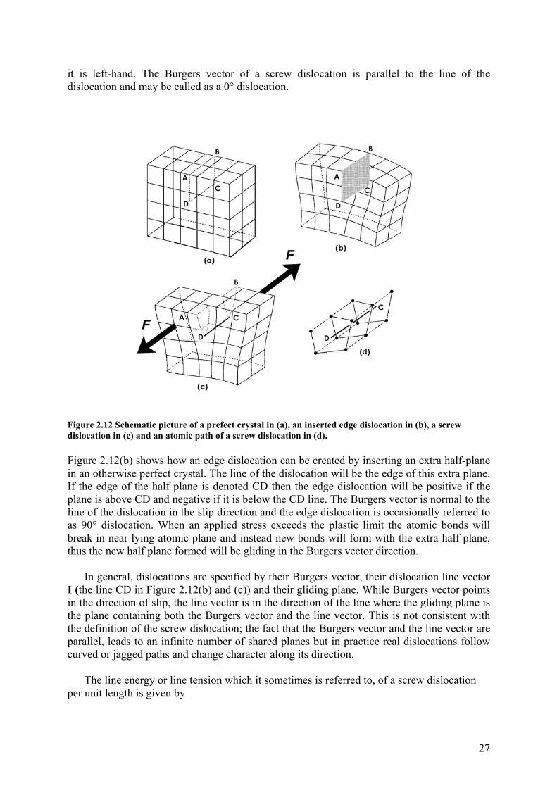
it is left-hand. The Burgers vector of a screw dislocation is parallel to the line of the dislocation and may be called as a 0° dislocation.
Figure 2.12 Schematic picture of a prefect crystal in (a), an inserted edge dislocation in (b), a screw dislocation in (c) and an atomic path of a screw dislocation in (d). Figure 2.12(b) shows how an edge dislocation can be created by inserting an extra half-plane in an otherwise perfect crystal. The line of the dislocation will be the edge of this extra plane. If the edge of the half plane is denoted CD then the edge dislocation will be positive if the plane is above CD and negative if it is below the CD line. The Burgers vector is normal to the line of the dislocation in the slip direction and the edge dislocation is occasionally referred to as 90° dislocation. When an applied stress exceeds the plastic limit the atomic bonds will break in near lying atomic plane and instead new bonds will form with the extra half plane, thus the new half plane formed will be gliding in the Burgers vector direction.
In general, dislocations are specified by their Burgers vector, their dislocation line vector I (the line CD in Figure 2.12(b) and (c)) and their gliding plane. While Burgers vector points in the direction of slip, the line vector is in the direction of the line where the gliding plane is the plane containing both the Burgers vector and the line vector. This is not consistent with the definition of the screw dislocation; the fact that the Burgers vector and the line vector are parallel, leads to an infinite number of shared planes but in practice real dislocations follow curved or jagged paths and change character along its direction.
The line energy or line tension which it sometimes is referred to, of a screw dislocation per unit length is given by
27

⎥⎦
⎤⎢⎣
⎡+⎟
⎠⎞
⎜⎝⎛= 1ln
4
2
bRGbEscrew π
, (24)
where ν is the Poisson’s ratio, G is the Shear modulus, b is the length of the Burgers vector and R is the outer radius of the dislocation. The line energy of an edge dislocation is given by
( ) ⎥⎦
⎤⎢⎣
⎡+⎟
⎠⎞
⎜⎝⎛
−= 1ln
14
2
bRGbEedge νπ
(25)
Real dislocations are often containing both a screw component and an edge component with no interactions between these two and the mixed energy is given by: ( )
( ) ⎥⎦
⎤⎢⎣
⎡+⎟
⎠⎞
⎜⎝⎛
−−
= 1ln14
cos1 22
bRGbEmix νπ
αν , (26)
where α is the angle between the Burgers vector and the line vector. For zinc blende and diamond crystals the angle is often observed to be 60° and the dislocations are called 60° dislocations.
The dependence on the type of dislocation is relatively weak and it may be written sometime as E ≈ CGb2 where the constant C has a value between 0.5 and 1. Frank’s rule is based on this and it says that if a dislocation reaction is energetically favorable so that the ∑b2 of the product is less than the ∑b2 for the reactants than it will take place. An example of this is the total annihilation of two identical Burgers vectors with opposite signs whose product equals 0 and still keeps the necessary condition of conservation of the Burgers vectors.
Fl, The line tension force of a dislocation segment residing in an interface has an expression similar to the one above. It is based on the similarity between the work W done to lengthen a dislocation by an amount dl since this corresponds to the line tension times this extra length. This may be written as W = Fdl and F = W/dl is the same as the line energy E (expressed per unit length). The outer radius R is set to equal the layer thickness h99 ( )
( ) ⎥⎦
⎤⎢⎣
⎡+⎟
⎠⎞
⎜⎝⎛
−−
= 1ln14
cos1 22
bhGbFl νπ
αν(27)
However, for an interface an average shear modulus D may be used instead of ( )νπ −1/Gb where D is defined as
( )( )νπ −+=
1sl
sl
GGbGG
D (28)
28

2.10.2.1 Critical thickness
One of the most used expressions for the critical thickness is the one derived from balancing forces working on the dislocation100. The resolved stress is given by eq. (11) and the force per unit length on the dislocation in the epilayer is λφσ coscosbFres = (29) The stress in the epitaxial film is 0,, === zyyxx YY σεσεσ (30) which for isotropic stress will be σ = σx = σy, σz = 0 with strains ε = εx = εy. For isotropic material the resolved force may be written as ( )
( ) λφενν coscos
112 bGFres −
+= (31)
which for the total force working on the dislocation equals ( )
( ) λενν
φcos
112
cosbhGhF
F rese −
+== . (32)
The critical thickness is then found from setting the line tension force (27) to equal the total lateral force working on the dislocation and the balancing (isotropic) result is ( ) ( )[ ]
( ) λνπεαν
cos181/lncos.1
22
++−
=bhb
h cc (33)
For anisotropic crystals Y should be substituted for 2G(1 + ν)/ (1 - ν) and D may be used.
2.10.2.2 Image forces
In order to reduce the total energy, dislocations with equal sign tend to repel each other whereas dislocation with opposite signs will be attracted and eventually annihilated101. Dislocations near a free surface will be attracted towards it because the material is effectively more compliant there and the dislocation energy is lower, for the same reason the dislocation will be repelled by a more rigid surface. The boundary conditions to fulfill on a free surface at x = 0 is that σxx, σyx and σzx all must be zero. These conditions are accomplished if an equal virtual dislocation, but with opposite sign, is placed on the opposite side of the free surface at the same distance to the interface, a so called mirrored dislocation. The resulting force
29
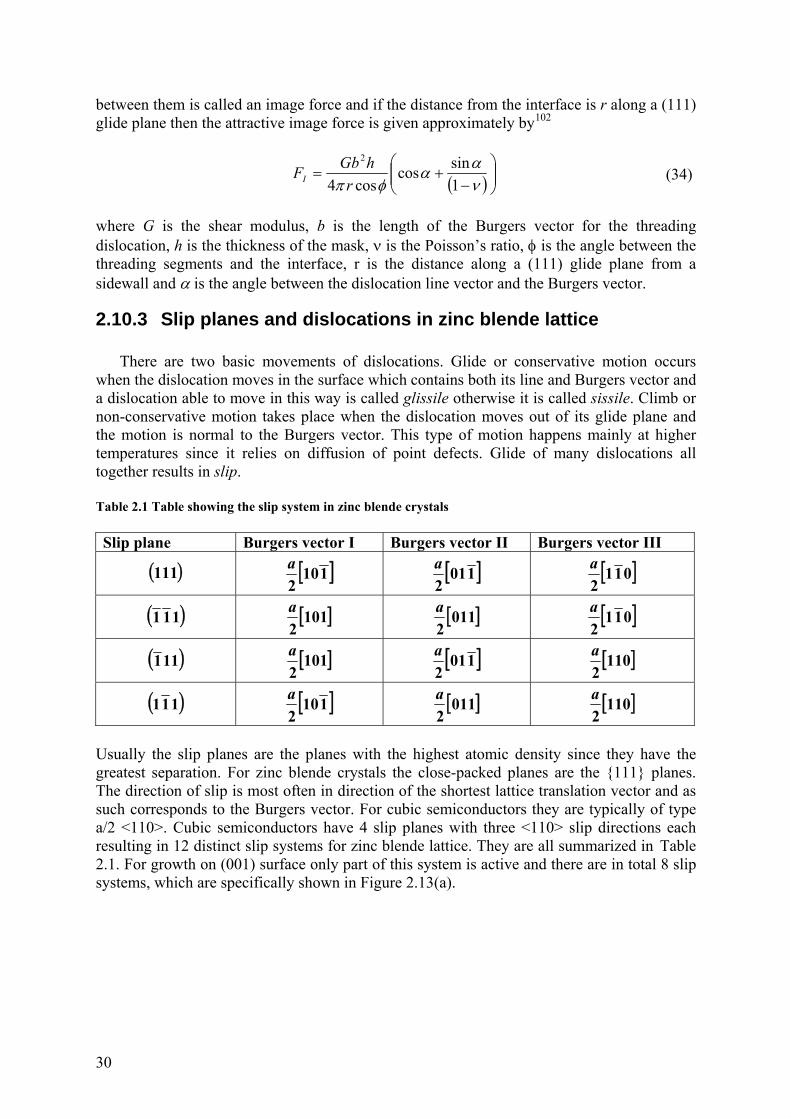
between them is called an image force and if the distance from the interface is r along a (111) glide plane then the attractive image force is given approximately by102
( )⎟⎟⎠
⎞⎜⎜⎝
⎛−
+=ναα
φπ 1sincos
cos4
2
rhGbFI (34)
where G is the shear modulus, b is the length of the Burgers vector for the threading dislocation, h is the thickness of the mask, ν is the Poisson’s ratio, φ is the angle between the threading segments and the interface, r is the distance along a (111) glide plane from a sidewall and α is the angle between the dislocation line vector and the Burgers vector.
2.10.3 Slip planes and dislocations in zinc blende lattice
There are two basic movements of dislocations. Glide or conservative motion occurs when the dislocation moves in the surface which contains both its line and Burgers vector and a dislocation able to move in this way is called glissile otherwise it is called sissile. Climb or non-conservative motion takes place when the dislocation moves out of its glide plane and the motion is normal to the Burgers vector. This type of motion happens mainly at higher temperatures since it relies on diffusion of point defects. Glide of many dislocations all together results in slip. Table 2.1 Table showing the slip system in zinc blende crystals Slip plane Burgers vector I Burgers vector II Burgers vector III
[ ]0112a
( )111 [ ]1102a
[ ]1012a
[ ]0112a
( )111 [ ]1012a
[ ]0112a
( )111 [ ]1012a
[ ]1012a
[ ]1102a
( )111 [ ]1102a
[ ]0112a
[ ]1102a
Usually the slip planes are the planes with the highest atomic density since they have the greatest separation. For zinc blende crystals the close-packed planes are the {111} planes. The direction of slip is most often in direction of the shortest lattice translation vector and as such corresponds to the Burgers vector. For cubic semiconductors they are typically of type a/2 <110>. Cubic semiconductors have 4 slip planes with three <110> slip directions each resulting in 12 distinct slip systems for zinc blende lattice. They are all summarized in Table 2.1. For growth on (001) surface only part of this system is active and there are in total 8 slip systems, which are specifically shown in Figure 2.13(a).
30
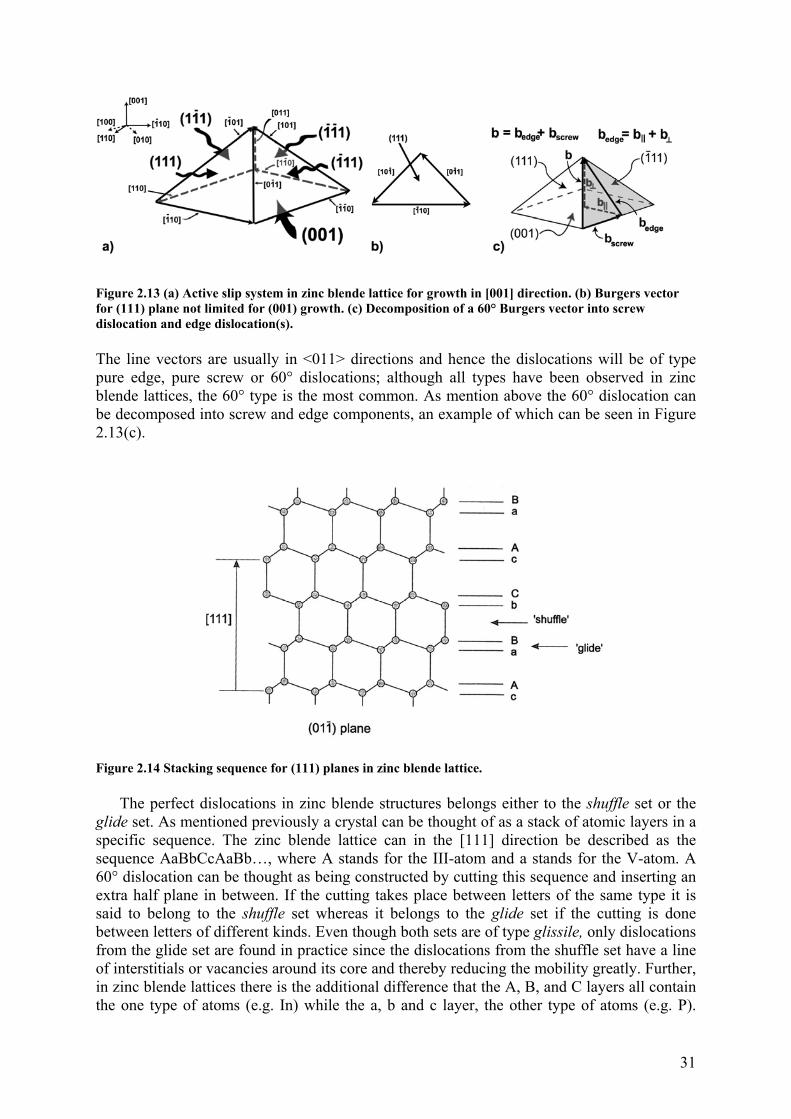
Figure 2.13 (a) Active slip system in zinc blende lattice for growth in [001] direction. (b) Burgers vector for (111) plane not limited for (001) growth. (c) Decomposition of a 60° Burgers vector into screw dislocation and edge dislocation(s). The line vectors are usually in <011> directions and hence the dislocations will be of type pure edge, pure screw or 60° dislocations; although all types have been observed in zinc blende lattices, the 60° type is the most common. As mention above the 60° dislocation can be decomposed into screw and edge components, an example of which can be seen in Figure 2.13(c).
Figure 2.14 Stacking sequence for (111) planes in zinc blende lattice.
The perfect dislocations in zinc blende structures belongs either to the shuffle set or the glide set. As mentioned previously a crystal can be thought of as a stack of atomic layers in a specific sequence. The zinc blende lattice can in the [111] direction be described as the sequence AaBbCcAaBb…, where A stands for the III-atom and a stands for the V-atom. A 60° dislocation can be thought as being constructed by cutting this sequence and inserting an extra half plane in between. If the cutting takes place between letters of the same type it is said to belong to the shuffle set whereas it belongs to the glide set if the cutting is done between letters of different kinds. Even though both sets are of type glissile, only dislocations from the glide set are found in practice since the dislocations from the shuffle set have a line of interstitials or vacancies around its core and thereby reducing the mobility greatly. Further, in zinc blende lattices there is the additional difference that the A, B, and C layers all contain the one type of atoms (e.g. In) while the a, b and c layer, the other type of atoms (e.g. P).
31
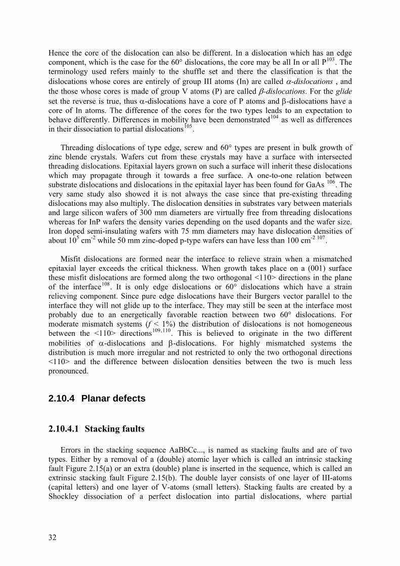
Hence the core of the dislocation can also be different. In a dislocation which has an edge component, which is the case for the 60° dislocations, the core may be all In or all P103. The terminology used refers mainly to the shuffle set and there the classification is that the dislocations whose cores are entirely of group III atoms (In) are called α-dislocations , and the those whose cores is made of group V atoms (P) are called β-dislocations. For the glide set the reverse is true, thus α-dislocations have a core of P atoms and β-dislocations have a core of In atoms. The difference of the cores for the two types leads to an expectation to behave differently. Differences in mobility have been demonstrated104 as well as differences in their dissociation to partial dislocations105.
Threading dislocations of type edge, screw and 60° types are present in bulk growth of zinc blende crystals. Wafers cut from these crystals may have a surface with intersected threading dislocations. Epitaxial layers grown on such a surface will inherit these dislocations which may propagate through it towards a free surface. A one-to-one relation between substrate dislocations and dislocations in the epitaxial layer has been found for GaAs 106. The very same study also showed it is not always the case since that pre-existing threading dislocations may also multiply. The dislocation densities in substrates vary between materials and large silicon wafers of 300 mm diameters are virtually free from threading dislocations whereas for InP wafers the density varies depending on the used dopants and the wafer size. Iron doped semi-insulating wafers with 75 mm diameters may have dislocation densities of about 105 cm-2 while 50 mm zinc-doped p-type wafers can have less than 100 cm-2 107.
Misfit dislocations are formed near the interface to relieve strain when a mismatched epitaxial layer exceeds the critical thickness. When growth takes place on a (001) surface these misfit dislocations are formed along the two orthogonal <110> directions in the plane of the interface108. It is only edge dislocations or 60° dislocations which have a strain relieving component. Since pure edge dislocations have their Burgers vector parallel to the interface they will not glide up to the interface. They may still be seen at the interface most probably due to an energetically favorable reaction between two 60° dislocations. For moderate mismatch systems (f < 1%) the distribution of dislocations is not homogeneous between the <110> directions109,110. This is believed to originate in the two different mobilities of α-dislocations and β-dislocations. For highly mismatched systems the distribution is much more irregular and not restricted to only the two orthogonal directions <110> and the difference between dislocation densities between the two is much less pronounced.
2.10.4 Planar defects
2.10.4.1 Stacking faults Errors in the stacking sequence AaBbCc..., is named as stacking faults and are of two
types. Either by a removal of a (double) atomic layer which is called an intrinsic stacking fault Figure 2.15(a) or an extra (double) plane is inserted in the sequence, which is called an extrinsic stacking fault Figure 2.15(b). The double layer consists of one layer of III-atoms (capital letters) and one layer of V-atoms (small letters). Stacking faults are created by a Shockley dissociation of a perfect dislocation into partial dislocations, where partial
32
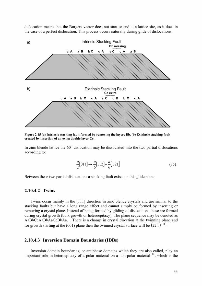
dislocation means that the Burgers vector does not start or end at a lattice site, as it does in the case of a perfect dislocation. This process occurs naturally during glide of dislocations.
Figure 2.15 (a) Intrinsic stacking fault formed by removing the layers Bb. (b) Extrinsic stacking fault created by insertion of an extra double layer Cc. In zinc blende lattice the 60° dislocation may be dissociated into the two partial dislocations according to: [ ] [ ] [ ]211
6112
6011
2aaa
+→ (35)
Between these two partial dislocations a stacking fault exists on this glide plane.
2.10.4.2 Twins
Twins occur mainly in the [111] direction in zinc blende crystals and are similar to the stacking faults but have a long range effect and cannot simply be formed by inserting or removing a crystal plane. Instead of being formed by gliding of dislocations these are formed during crystal growth (bulk growth or heteroepitaxy). The plane sequence may be denoted as AaBbCcAaBbAaCcBbAa… There is a change in crystal direction at the twinning plane and for growth starting at the (001) plane then the twinned crystal surface will be ( 122 )111.
2.10.4.3 Inversion Domain Boundaries (IDBs)
Inversion domain boundaries, or antiphase domains which they are also called, play an important role in heteroepitaxy of a polar material on a non-polar material112, which is the
33
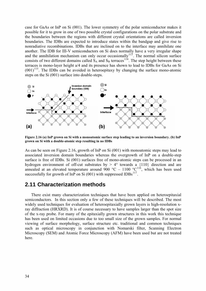
case for GaAs or InP on Si (001). The lower symmetry of the polar semiconductor makes it possible for it to grow in one of two possible crystal configurations on the polar substrate and the boundaries between the regions with different crystal orientations are called inversion boundaries. The IDBs are expected to introduce states within the bandgap and give rise to nonradiative recombinations. IDBs that are inclined on to the interface may annihilate one another. The IDB for III-V semiconductors on Si does normally have a very irregular shape and the annihilation mechanism can only occur occasionally113. The normal silicon surface consists of two different domains called SA and SB terraces114. The step height between these terraces is mono-layer height a/4 and its presence has shown to lead to IDBs for GaAs on Si (001)115. The IDBs can be avoided in heteroepitaxy by changing the surface mono-atomic steps on the Si (001) surface into double-steps.
Figure 2.16 (a) InP grown on Si with a monoatomic surface step leading to an inversion boundary. (b) InP grown on Si with a double-atomic step resulting in no IDBs As can be seen on Figure 2.16, growth of InP on Si (001) with monoatomic steps may lead to associated inversion domain boundaries whereas the overgrowth of InP on a double-step surface is free of IDBs. Si (001) surfaces free of mono-atomic steps can be processed in an hydrogen environment of off-cut substrates by > 4° towards a {110} direction and are annealed at an elevated temperature around 900 °C – 1100 °C116, which has been used successfully for growth of InP on Si (001) with suppressed IDBs117. 2.11 Characterization methods
There exist many characterization techniques that have been applied on heteroepitaxial semiconductors. In this section only a few of these techniques will be described. The most widely used techniques for evaluation of heteroepitaxially grown layers is high-resolution x-ray diffraction (HRXRD). It is of course necessary to have samples larger than the spot size of the x-ray probe. For many of the epitaxially grown structures in this work this technique has been used on limited occasions due to too small size of the grown samples. For normal viewing of surface morphology, surface structure etc. traditional and common techniques such as optical microscopy in conjunction with Nomarski filter, Scanning Electron Microscopy (SEM) and Atomic Force Microscopy (AFM) have been used but are not treated here.
34
2.11.1 High resolution X-ray diffraction
High resolution x-ray diffraction (HRXRD) is important in the structural characterization of heteroepitaxial layers, revealing lattice constants, strains, crystallographic orientations and defect densities. The principle of this technique is based on the elastic scattering of x-ray radiation by the crystal lattice structure and the collection of scattered signal by an open detector or a crystal analyzer. The information of crystal structure and the distance between two scattering crystal planes can be obtained by Bragg’s Law: λθ nd =sin2 (36) where λ is the x-ray wavelength, θ is the angle between the incident x-ray beam and the surface of a set of scattering planes and d is the spacing between the planes, which for cubic crystals with lattice constant a takes the simple expression
( )222)(
lkhahkld
++= (37)
A schematic view of a typical x-ray diffractometer can be seen in Figure 2.17 below. The source consists of a Cu x-ray source with a small angular divergence. The Cu Kα1 (λ=1.5406 Å) radiation is separated from other radiation components in a monochromator like in (c)
Figure 2.17. (a) Picture of goniometer used to manipulate the sample (ω is x-ray incident angle, θ is Bragg angle, ϕ is rotation angle, χ is tilt angle). (b) Intensity and shape after x-ray beam passing through successive number of reflections in a channel-cut 220 Si crystal. (c) Channel cut Si 220 crystal with two configurations where (1) is for narrow FWHM of the beam (high resolution) and (2) is for high intensity. (d) Exaggerated picture of diffused scattering where the beam is collimated into the detector either by a slit or by passing through a crystal118.
35
where different configurations can be used either to achieve a narrow beam with high resolution or keeping the intensity high. In the goniometer (a) the sample can be tilted, rotated in two independent directions making it possible to vary independently the angle of incidence ω, the diffraction angle 2θ, the angle ϕ of rotation around the surface normal, and the angle χ of rotation around an in plane surface direction. The detector can often be set in either a receiving-slit mode, which is used to record rocking curve (RC), or in a triple-axis mode, which is ideal for reciprocal lattice mapping (RLM) measurement. A crystal analyzer is placed after the specimen and before the detector, in order to restrict its angular acceptance to ~12 arcsec and leads to the triple axis mode. This has the effect of separating the effects of strains and tilts on the measurement.
2.11.1.1 Strain
The strain in heteroepitaxy can be obtained by considering a tetragonal distorted film using the elasticity theory
1−=⊥
⊥S
layer
aa
ε (38)
⎟⎟⎠
⎞⎜⎜⎝
⎛×−= ⊥
12
11// 2C
Cεε (39)
where aS is the lattice constant of bulk substrate, and C11 and C12 are the elastic constants of the layer material at room temperature. The lattice constant parallel to the growth direction, a⊥ can be calculated from the Bragg angles of the substrate, θS and the layer, θLayer:
layer
SSlayer aa
θθ
sinsin
×= ⊥⊥ (40)
2.11.2 Photoluminescence
Photoluminescence (PL) consists of analyzing the luminescence spectra that appears from a structure when it is illuminated by a light source, most often a laser with a specific wavelength (of higher energy than the bandgap of the semiconductor). The laser light will create electron – hole pairs which will recombine via either a radiative or a non-radiative recombination process. The PL intensity, emission line width and wavelength can supply information on the electronic structure of the analyzed material. PL has been used to characterize heterostructures in order to examine the strain, such as for InGaAs/GaAs119,120, GaAs/Si121 and InP/Si122 and for spatially-resolved images of photoluminescence degradation due to non-radiative defects which appear dark since the number of non-radiative centers increases in the vicinity of the dislocation123.The PL intensity124 and PL broadening125 have also been used for determination of the critical thickness in InGaAs/GaAs quantum wells and strained layers, and it has been established in these works that a decrease in PL intensity and broadening in PL emission peak are due to the presence of non-radiative centers associated with misfit dislocations.
In heteroepitaxy where the lattice constant of the layers exceeds that of the substrate the layer will be under biaxial compressive strain. The strain can be decomposed into its
36
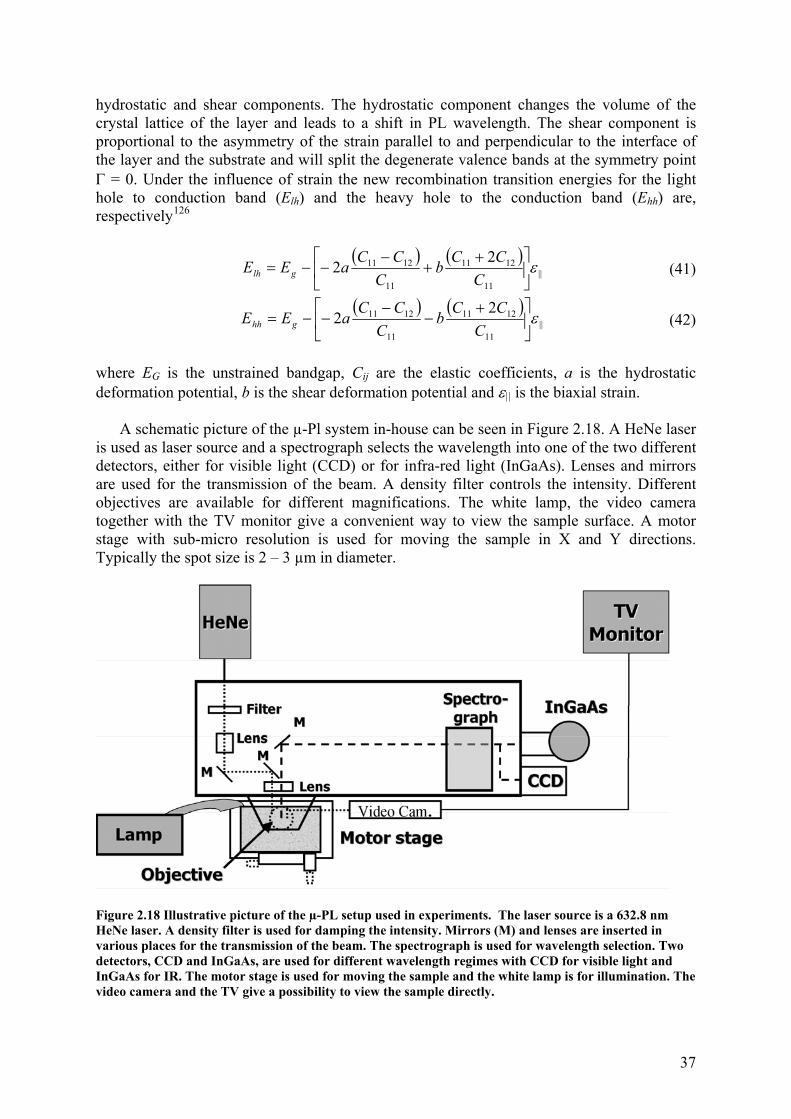
hydrostatic and shear components. The hydrostatic component changes the volume of the crystal lattice of the layer and leads to a shift in PL wavelength. The shear component is proportional to the asymmetry of the strain parallel to and perpendicular to the interface of the layer and the substrate and will split the degenerate valence bands at the symmetry point Γ = 0. Under the influence of strain the new recombination transition energies for the light hole to conduction band (Elh) and the heavy hole to the conduction band (Ehh) are, respectively126
( ) ( )
||11
1211
11
1211 22 ε⎥⎦
⎤⎢⎣
⎡ ++
−−−=
CCCb
CCCaEE glh (41)
( ) ( )||
11
1211
11
1211 22 ε⎥⎦
⎤⎢⎣
⎡ +−
−−−=
CCCb
CCCaEE ghh (42)
where EG is the unstrained bandgap, Cij are the elastic coefficients, a is the hydrostatic deformation potential, b is the shear deformation potential and ε|| is the biaxial strain.
A schematic picture of the µ-Pl system in-house can be seen in Figure 2.18. A HeNe laser is used as laser source and a spectrograph selects the wavelength into one of the two different detectors, either for visible light (CCD) or for infra-red light (InGaAs). Lenses and mirrors are used for the transmission of the beam. A density filter controls the intensity. Different objectives are available for different magnifications. The white lamp, the video camera together with the TV monitor give a convenient way to view the sample surface. A motor stage with sub-micro resolution is used for moving the sample in X and Y directions. Typically the spot size is 2 – 3 µm in diameter.
Figure 2.18 Illustrative picture of the µ-PL setup used in experiments. The laser source is a 632.8 nm HeNe laser. A density filter is used for damping the intensity. Mirrors (M) and lenses are inserted in various places for the transmission of the beam. The spectrograph is used for wavelength selection. Two detectors, CCD and InGaAs, are used for different wavelength regimes with CCD for visible light and InGaAs for IR. The motor stage is used for moving the sample and the white lamp is for illumination. The video camera and the TV give a possibility to view the sample directly.
37
2.11.3 Cathodoluminescence
Cathodoluminescence is similar to PL except that an electron beam (e-beam) is used for excitation. Whereas the PL emission may depend on the excitation wavelength, the CL excitation due to the e-beam leads to excitation of all different mechanisms present in the semiconductor. The radiative recombination is lower in the vicinity of a defect and by mapping the position of the e-beam an image containing relative radiative recombination luminescence can be obtained where threading dislocations may look like dark points and misfit dislocation appears as dark lines Moreover, the benefit of CL compared to PL lies in the high spatial resolution from the small size of the electron beam probe and the possibility of varying the electron beam energy, thus giving a more depth resolved information. Often the CL system is in-built in a traditional SEM system and SEM-CL imaging has been used to study misfit dislocations in InGaAs/InP single heterostructures127.
2.11.4 Crystallographic etching
A common method to evaluate dislocation densities in heteroepitaxy is the use of crystallographic etchants. These etchants will reveal the points of emergence of dislocations as hillocks or as etch pits. The physics behind this is the strained region surrounding the dislocation which will enhance or reduce the etch rate. The number of etch pits are counted by the use of Nomarski phase contrast microscopy, SEM or AFM. The number of etch pits is considered to correspond to the number of threading dislocations and the etch pit density (EPD) can thus be used for determination of the threading dislocation density. Sometimes the EPD is found to be much lower than the threading dislocation density which has been extracted from TEM measurements128. The explanation for this discrepancy has been found to be caused by a second set of dislocation pits that may be observed in TEM129. An underestimation of the real dislocation density may come from closely spaced dislocations that may produce one single etch pit and thus changing the assumed one-ton-one correspondence between etch pit and dislocation130. The overlap of near lying dislocations sets an upper limit for the dislocation density than can accurately be revealed by EPD and lies in the range 106 – 108 cm-2. A practical etchant to use for EPD on InP is the use of Hubert’s solution 2H3PO4:1HBr131 which has been proved to work efficiently on ELOG of InP on precoated silicon substrates for 20 seconds at room temperature.
2.11.5 Transmission Electron Microscopy
Transmission electron microscopy is a powerful instrument and is capable of revealing dislocation, stacking faults and other crystalline faults in epitaxial layers. The requirement for successful measurement is a thin enough sample for the transmission of electrons and that the sample is stable during exposure. The thinning of sample is the most difficult part in using TEM since the necessary condition is a sample size in the range of ~ 100 nm and the sample preparation, which may be done by for example ion milling, may introduce new defects and may also in turn create in-built strain. The operation of a TEM is shown schematically in
38
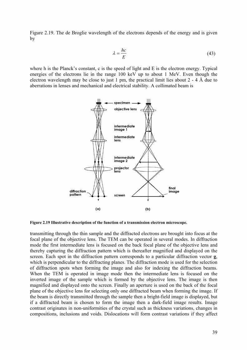
Figure 2.19. The de Broglie wavelength of the electrons depends of the energy and is given by
Ehc
=λ (43)
where h is the Planck’s constant, c is the speed of light and E is the electron energy. Typical energies of the electrons lie in the range 100 keV up to about 1 MeV. Even though the electron wavelength may be close to just 1 pm, the practical limit lies about 2 - 4 Å due to aberrations in lenses and mechanical and electrical stability. A collimated beam is
Figure 2.19 Illustrative description of the function of a transmission electron microscope. transmitting through the thin sample and the diffracted electrons are brought into focus at the focal plane of the objective lens. The TEM can be operated in several modes. In diffraction mode the first intermediate lens is focused on the back focal plane of the objective lens and thereby capturing the diffraction pattern which is thereafter magnified and displayed on the screen. Each spot in the diffraction pattern corresponds to a particular diffraction vector g, which is perpendicular to the diffracting planes. The diffraction mode is used for the selection of diffraction spots when forming the image and also for indexing the diffraction beams. When the TEM is operated in image mode then the intermediate lens is focused on the inverted image of the sample which is formed by the objective lens. The image is then magnified and displayed onto the screen. Finally an aperture is used on the back of the focal plane of the objective lens for selecting only one diffracted beam when forming the image. If the beam is directly transmitted through the sample then a bright-field image is displayed, but if a diffracted beam is chosen to form the image then a dark-field image results. Image contrast originates in non-uniformities of the crystal such as thickness variations, changes in compositions, inclusions and voids. Dislocations will form contrast variations if they affect
39
the diffracting crystal planes so that their separation or orientation changes. Solution for the equations of the transmitted intensity contains a factor g⋅u, where u is the displacement vector by which atoms are displaced from their original position. When g⋅u = 0 there is no change in intensity. The dislocation will appear as a dark line in bright-field image or as a bright line in dark-field image. The invisible criteria g⋅u = 0 may be used to determine the Burgers vector since when g is perpendicular to b, then g⋅u = g⋅b = 0. If the sample is tilted, two sets of diffracting planes, g1 and g2, can be found for which the invisible criteria holds and then b must be perpendicular to both g1 and g2, thus has the direction g1 × g2. 2.12 Background on applications
This thesis includes two papers on buried heterostructure devices in which selective epitaxy or specifically, semi-insulating InP:Fe regrowth has been used. The first one deals with regrowth of InP:Fe around aluminum-containing multi quantum wells. The second one on reactive ion etching and regrowth of arrayed waveguide gratings (AWGs) used in encoder/decoder systems for optical code-division multiple-access (O-CDMA). The focus on these devices in this thesis is on the regrowth aspects. These two application areas are very vast, but a short background on lasers and AWG structures will be given here. More detailed treatments can be found elsewhere on lasers132,133 and on arrayed waveguide gratings134.
2.12.1 Semiconductor lasers
The semiconductor laser consists of a resonant cavity with two mirrors and a photon generating material (gain or active medium) in between. There are three transitions that are important in semiconductor lasers that occur between the conduction and valence bands of the material, namely the absorption, the spontaneous emission and the stimulated emission process. In the absorption process an electron in the valence band gains energy by absorbing a photon, exciting it to a higher energy level in the conduction band. For the spontaneous emission an electron starts out in an excited state in the conduction band. When the electron falls back into the valence band it releases its excess energy in the form of a photon where the photon emitted by the electron decaying to a lower energy has a random phase and direction. For the third process, the stimulated emission, a photon is strongly coupled with an electron, it can cause the electron to decay to a lower energy level, releasing a photon of the same energy. The emitted photon has the same direction and phase as the incident photon. If the stimulated emission is to dominate over the spontaneous emission a necessary condition is the so called population inversion, i.e., the population of electrons in the conduction band is larger than that in the valence band. For lasing, it is necessary that the build up of photons in the cavity, i.e., the optical gain, equals the losses through the mirrors and in the cavity. The coupling of optical power out from the medium is taken from one of the mirrors.
Examples of typical laser geometries can bee seen in Figure 2.20(a) – (d), from the simple double heterostructure (a) to the distributed feedback (DFB) (d). The insertion of semi-isolated material around the laser mesa leads to current confinement and a reduced current for lasing. Thin mesas will block some optical modes in the waveguide and will eventually make it single-mode if thin enough. The insertion of a Bragg grating has the purpose of picking one single longitudinal mode and suppressing the other. Most semiconductor lasers are electrically pumped. The active layer is surrounded by two layers of higher bandgap and
40
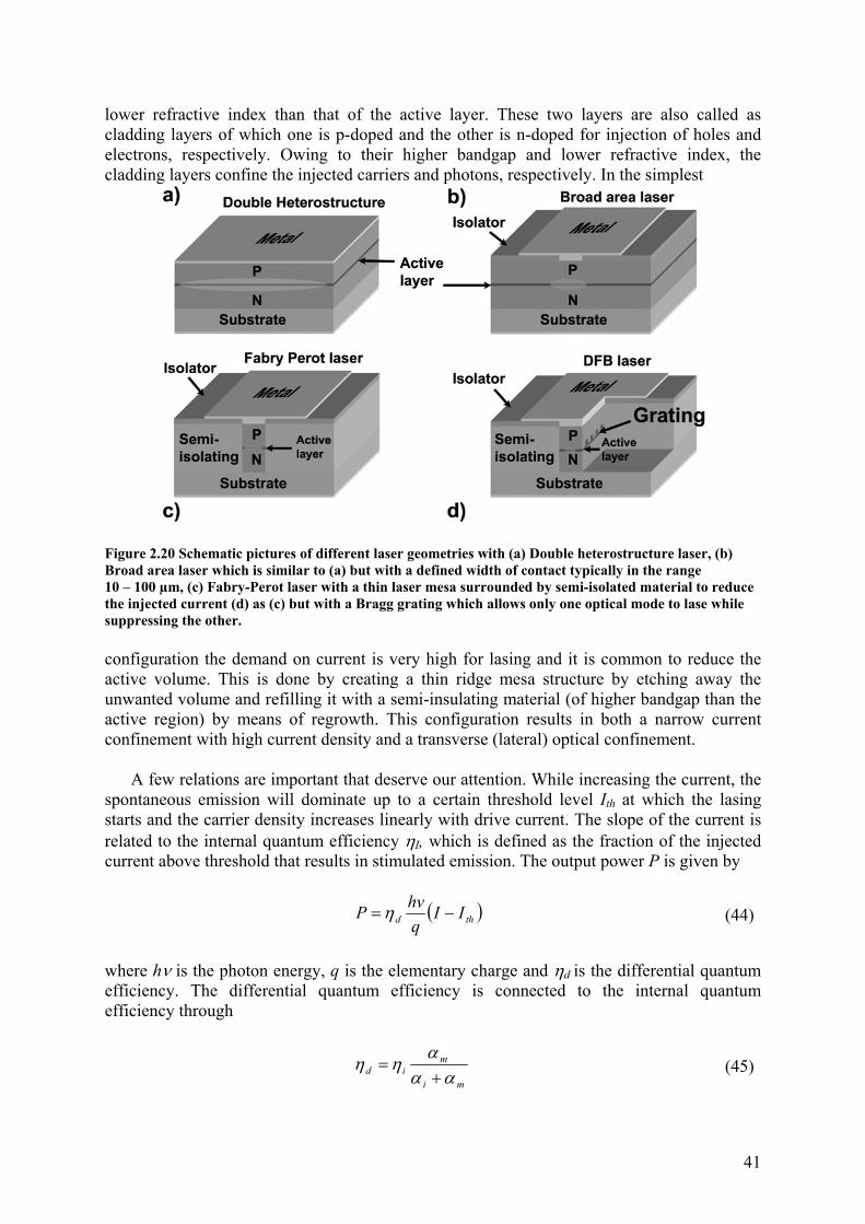
lower refractive index than that of the active layer. These two layers are also called as cladding layers of which one is p-doped and the other is n-doped for injection of holes and electrons, respectively. Owing to their higher bandgap and lower refractive index, the cladding layers confine the injected carriers and photons, respectively. In the simplest
Figure 2.20 Schematic pictures of different laser geometries with (a) Double heterostructure laser, (b) Broad area laser which is similar to (a) but with a defined width of contact typically in the range 10 – 100 µm, (c) Fabry-Perot laser with a thin laser mesa surrounded by semi-isolated material to reduce the injected current (d) as (c) but with a Bragg grating which allows only one optical mode to lase while suppressing the other. configuration the demand on current is very high for lasing and it is common to reduce the active volume. This is done by creating a thin ridge mesa structure by etching away the unwanted volume and refilling it with a semi-insulating material (of higher bandgap than the active region) by means of regrowth. This configuration results in both a narrow current confinement with high current density and a transverse (lateral) optical confinement.
A few relations are important that deserve our attention. While increasing the current, the spontaneous emission will dominate up to a certain threshold level Ith at which the lasing starts and the carrier density increases linearly with drive current. The slope of the current is related to the internal quantum efficiency ηI, which is defined as the fraction of the injected current above threshold that results in stimulated emission. The output power P is given by ( )thd II
qhvP −= η (44)
where hν is the photon energy, q is the elementary charge and ηd is the differential quantum efficiency. The differential quantum efficiency is connected to the internal quantum efficiency through
mi
mid αα
αηη
+= (45)
41
where αm is the mirror loss and αi is the internal modal loss in the cavity. The mirror loss is in turn related to the reflectivity of the facets r1 and r2 and the cavity length L from αm = L-1 ln(r1r2)-1.
The stimulated emission may either be driven by injecting electrons and holes, which we call electrical pumping or by direct photonic stimulation, which we call optical pumping.
When the laser is made very narrow, there will only be one transverse mode in the optical cavity. The modal optical gain (or loss) measurements in a single transverse-mode optical waveguide structure can be performed using the Hakki–Paoli method135, ,136 137. The Fabry-Perot (FP)-laser is biased below threshold and the amplified spontaneous emission (ASE) is collected from one of the laser facets using an anti-reflection coated lens coupled to a single-mode fiber with a built-in polarizer/isolator. The net modal gain is obtained from the ratio of the maximum intensity Imax and the minimum intensity Imin of the ASE as follows
minet SS
LgG αα +⎟
⎠⎞
⎜⎝⎛
+−
=−Γ=11ln1 , (46)
where minmax / IIS = , Γ is the electron- photon overlap factor referred to as the confinement factor, g is the material gain and L is the FP cavity length. A more accurate method to measure the optical gain for an FP cavity is by using the analytical expression to fit the ASE138. ( )( )( )
( ) ( ) 2sin41
111)(
221
221
22
21 ν
ηη
ν hkLerrerr
ererASE
i
sp
gLgL
gLgL
+−
−−−= (47)
Here k = 2π/λ and ηsp is the population inversion factor.
A final parameter which is presented here is the chirp factor αH, which is an important parameter for directly modulated laser and it is related to the frequency change of the laser during modulation. The frequency chirping δf in a directly modulated laser is given by
Naf gH δνπ
αδ Γ=
4, (48)
where νg is the group velocity of the optical waveguide mode, a = dg/dN is the differential gain and N is the carrier density in the quantum well.
2.12.2 Arrayed Waveguide Gratings (AWG)
Integrated arrayed waveguide gratings, or phased-array (de)multiplexers as they also are called, were first proposed in 1988 by Smit139 and was further extended from l × N to N × N devices by Dragone140. A typical AWG can be seen in Figure 2.21 and consists of two focusing slab regions or free propagation regions (FPR) with a number of waveguides connected between them with a constant path length difference ΔL, where ΔL will equal an integer number of the central wavelength λc for the AWG.
42
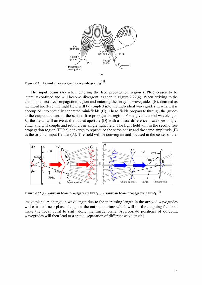
Figure 2.21. Layout of an arrayed waveguide grating141.
The input beam (A) when entering the free propagation region (FPR1) ceases to be laterally confined and will become divergent, as seen in Figure 2.22(a). When arriving to the end of the first free propagation region and entering the array of waveguides (B), denoted as the input aperture, the light field will be coupled into the individual waveguides in which it is decoupled into spatially separated mini-fields (C). These fields propagate through the guides to the output aperture of the second free propagation region. For a given central wavelength, λc, the fields will arrive at the output aperture (D) with a phase difference = m2π (m = 0, 1, 2….), and will couple and rebuild one single light field. The light field will in the second free propagation region (FPR2) converge to reproduce the same phase and the same amplitude (E) as the original input field at (A). The field will be convergent and focused in the center of the
Figure 2.22 (a) Gaussian beam propagates in FPR1. (b) Gaussian beam propagates in FPR2. 142. image plane. A change in wavelength due to the increasing length in the arrayed waveguides will cause a linear phase change at the output aperture which will tilt the outgoing field and make the focal point to shift along the image plane. Appropriate positions of outgoing waveguides will then lead to a spatial separation of different wavelengths.
43

Figure 2.23 Geometry of the receiver part of the AWG.
A few relations for the most important properties will here be given. The focusing is obtained by choosing the path length difference ΔL as an integer number of the central wavelength of the arrayed waveguides
g
cN
mLλ
=Δ (49)
where m is order of the arrayed waveguide grating, λc is the central wavelength in vacuum and Ng is the effective index of the waveguide mode. The array of waveguides will with this choice act as a lens with object and image plane at a radial distance of Ra from the arrayed waveguides apertures. The dispersion angle can be found from ( 2 / )sin[ ]FPR
a FPR a
m mad d
2φ π β φ πθβ
Δ − Δ −= ≈ , (50)
where Δφ = βΔL and β and βFPR are the propagation constants of the waveguide mode and the slab mode in the free propagation region, respectively, and da is the lateral spacing between center lines in adjacent waveguides at the aperture. The dispersion D of the array is defined as the lateral displacement ds of the focal point per unit change of the frequency. Form Figure 2.23 it follows that '
ga
c FPR
N Lds dD Rdf df f N
θα
Δ= = =
Δ(51)
in which fc is the central frequency NFPR is the slab mode index of the free propagation region and Δα = da/Ra is the divergence angle between the arrayed waveguides, and N´g is the group index of the waveguide mode
44
' gg g
dNN N f
df= + (52)
The output of the arrayed waveguides is periodical and after each change of 2π for Δφ
the field will be repeated. This period in the frequency domain is denoted as the free spectral range and is given by
'F S Rg
cfN L
Δ =Δ
(53)
For other important aspects, such as insertion loss, non-uniformity and bandwidth which
can be obtained by applying a Gaussian bean approximation the reader is advised to reference [141]. In this reference, different sources for crosstalks are dealt with, however two of them are directly related to imperfections in the fabrication process and will be shortly mentioned here. Deviations in the propagation constant in the arrayed waveguides may lead to large error in the phase transfer with a resulting increased level of crosstalk. The error may come from small local deviations of the composition, film thickness, waveguide width or inhomogeneous filling of the gap between the waveguides at the apertures. Another source for crosstalk is radiative scattering taking place at rough sidewalls of the waveguides or at junctions.
45

46
3 Summary of results and discussions
In this chapter we summarize and discuss the major results obtained in this thesis.
(i) The first part deals with the special case of selective epitaxy, commonly denoted as selective regrowth on (or planarization) of non-planar structures. The non-planar structures consist of the mesa parts (normally masked and unetched) and the remaining parts are unmasked and etched, and hence the non-planarity. The growth on this area fills the etched parts and hence it is called regrowth. Besides, it grows only in the unmasked and etched areas and hence it is called selective regrowth. Selective regrowth is complicated from the crystal growth point of view. But as a simple description, one can state that under HVPE growth conditions, it takes place laterally from the masked mesa parts and as normal growth on the unmasked areas. The contributions of lateral growth and normal growth vary according to the etched depth, distance between the mesas, growth conditions etc. This process will act as a planarization of the etched non-planar surface. It is useful for both stabilizing the active regions normally contained in the unetched mesa parts. This can also provide current confinement in the active regions when the regrown material has semi-insulating properties. This section starts with an appraisal and characterization of regrowth of semi-insulating InP:Fe around arrayed waveguide structures. The intricacy in these structures is that after etching, it exposes surfaces in every possible angle or crystallographic direction. Paper A and Paper B are the examples of applications where the HVPE regrowth is an essential part of the device fabrication and where the beneficial growth properties of HVPE are fully utilized.
(ii) The second part addresses selective epitaxy on planar surfaces. Here the area for growth is partly masked and partly open (unmasked). The surface is not etched as in the previous case. We explore in Paper C a special case where the masked area is large in comparison with the open area. Here the surface is planar but the major part of the area is masked and only a small portion is open. We are the first to address this special case. Selective epitaxy is often conducted on areas which contain larger open area than the masked area.
(iii) The third part addresses a special case of selective epitaxy, called heteroepitaxy. This offers the flexibility of growing a material on a substrate, which is partly masked. Here, the substrate material and the grown material are completely different and with different lattice constants. We employ a method called Epitaxial Lateral Overgrowth (ELOG) to obtain InP on Si or SOI (silicon on insulator). The aim of the studies is to obtain a layer of ELOG InP with good crystal quality with least defects. In ELOG, the growth starts in openings containing a InP seed layer (with a high dislocation density) on Si or SOI followed by mask encroachment, i.e., the growth that started in the openings proceed laterally on the mask. The
47
quality of the ELOG layer is such that it is purer on the masked area than that above the openings. Paper D studies the application of ELOG of InP on SOI. The SOI wafer is an exact-oriented (001) substrate instead of a 4° off-oriented Si wafer. This is the first report of InP on SOI. In Paper E the material strain properties of ELOG InP on Si are presented. Finally, Paper F, Paper G and Paper H give a systematic approach on an effective pattern design to filter off the defects even in the ELOG region above the openings. We deploy nano-size openings instead of the previously used micro-size openings. Thereby we reap the benefits of nano-ELOG for dislocation filtering as well as to grow relatively thin (~1 µm) ELOG InP layers.
3.1 Deep etching and regrowth of dense arrayed waveguide gratings
An important piece of work in this thesis concerns selective regrowth of InP:Fe for integration of devices. A major part is devoted to the study of regrowth around Arrayed Waveguide Gratings (AWGs) on InP platform in view of creating an integrated photonic chip for Optical Code Division Multiplex Access (O-CDMA). The work included process developments and optimization specific to this purpose as it is novel: reactive ion etching (RIE), wafer cleaning procedure, mass transport within the etched arrayed waveguide grating mesas and selective regrowth. Below we describe these one by one.
3.1.1 Reactive ion etching The etching of waveguides needs to fulfill the following requirements:
• Accurate control of etch depth and uniformity • Smooth sidewalls to reduce roughness • Unchanged width of waveguides • Control of impurities and etch damages
The control of etch depth and uniformity was found to be improved by insertion of an etch load dummy wafer. The etch rate is proportional to the amount of material to be etched due to the consumption of etching reaction of the gas species with the sample(s). This creates local differences in drainage of source species and leads to faster etch rate at the edges and also to slower etching in regions with dense waveguides due to the larger exposed surface. Insertion of a load and dummy wafer beneath the samples improved the uniformity from typically ± 0.4 µm to about ± 0.2 µm, and even down to ± 0.1 µm if the outermost edge area within 1 mm is omitted. The edge effect is shifted from the edges of the sample to the edges of the dummy wafer, which in our experiments is either a 2 inch or 3 inch wafer. However, the topographic difference between the sample and the wafer below will still lead to a small edge effect. Etching with CH4 and H2 creates polymers which preferably stick to the mask and help to prevent the mask from being etched. The etch damages can be reduced by decreasing the bias but this will enhance the chance for building of polymers on the semiconductor surface which will set a threshold on the smallest bias. The main challenge in the RIE equipment that has been used has been to keep the sidewall roughness to a minimum while preserving the width of the waveguides. This was found to be a trade-off and excellent
48
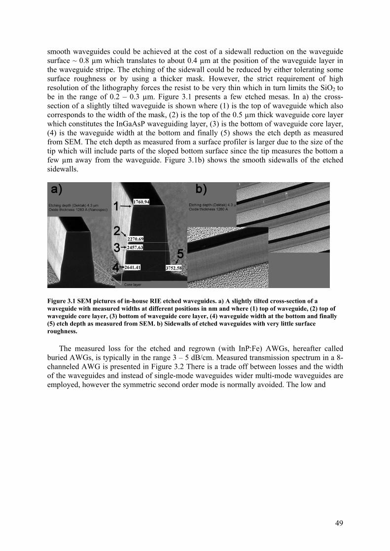
smooth waveguides could be achieved at the cost of a sidewall reduction on the waveguide surface ~ 0.8 µm which translates to about 0.4 µm at the position of the waveguide layer in the waveguide stripe. The etching of the sidewall could be reduced by either tolerating some surface roughness or by using a thicker mask. However, the strict requirement of high resolution of the lithography forces the resist to be very thin which in turn limits the SiO2 to be in the range of 0.2 – 0.3 µm. Figure 3.1 presents a few etched mesas. In a) the cross-section of a slightly tilted waveguide is shown where (1) is the top of waveguide which also corresponds to the width of the mask, (2) is the top of the 0.5 µm thick waveguide core layer which constitutes the InGaAsP waveguiding layer, (3) is the bottom of waveguide core layer, (4) is the waveguide width at the bottom and finally (5) shows the etch depth as measured from SEM. The etch depth as measured from a surface profiler is larger due to the size of the tip which will include parts of the sloped bottom surface since the tip measures the bottom a few µm away from the waveguide. Figure 3.1b) shows the smooth sidewalls of the etched sidewalls.
Figure 3.1 SEM pictures of in-house RIE etched waveguides. a) A slightly tilted cross-section of a waveguide with measured widths at different positions in nm and where (1) top of waveguide, (2) top of waveguide core layer, (3) bottom of waveguide core layer, (4) waveguide width at the bottom and finally (5) etch depth as measured from SEM. b) Sidewalls of etched waveguides with very little surface roughness.
The measured loss for the etched and regrown (with InP:Fe) AWGs, hereafter called buried AWGs, is typically in the range 3 – 5 dB/cm. Measured transmission spectrum in a 8- channeled AWG is presented in Figure 3.2 There is a trade off between losses and the width of the waveguides and instead of single-mode waveguides wider multi-mode waveguides are employed, however the symmetric second order mode is normally avoided. The low and
49
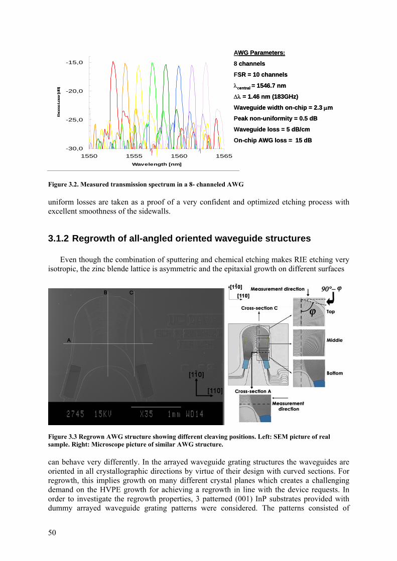
-30,0
-25,0
-20,0
-15,0
1550 1555 1560 1565Wavelength [nm]
Exce
ss L
ossr
[dB]
AWG Parameters:
8 channels
FSR = 10 channels
λcentral = 1546.7 nm
Δλ = 1.46 nm (183GHz)
Waveguide width on-chip = 2.3 μm
Peak non-uniformity = 0.5 dB
Waveguide loss = 5 dB/cm
On-chip AWG loss = 15 dB-30,0
-25,0
-20,0
-15,0
1550 1555 1560 1565Wavelength [nm]
Exce
ss L
ossr
[dB]
AWG Parameters:
8 channels
FSR = 10 channels
λcentral = 1546.7 nm
Δλ = 1.46 nm (183GHz)
Waveguide width on-chip = 2.3 μm
Peak non-uniformity = 0.5 dB
Waveguide loss = 5 dB/cm
On-chip AWG loss = 15 dB
Figure 3.2. Measured transmission spectrum in a 8- channeled AWG uniform losses are taken as a proof of a very confident and optimized etching process with excellent smoothness of the sidewalls.
3.1.2 Regrowth of all-angled oriented waveguide structures Even though the combination of sputtering and chemical etching makes RIE etching very isotropic, the zinc blende lattice is asymmetric and the epitaxial growth on different surfaces
Figure 3.3 Regrown AWG structure showing different cleaving positions. Left: SEM picture of real sample. Right: Microscope picture of similar AWG structure. can behave very differently. In the arrayed waveguide grating structures the waveguides are oriented in all crystallographic directions by virtue of their design with curved sections. For regrowth, this implies growth on many different crystal planes which creates a challenging demand on the HVPE growth for achieving a regrowth in line with the device requests. In order to investigate the regrowth properties, 3 patterned (001) InP substrates provided with dummy arrayed waveguide grating patterns were considered. The patterns consisted of
50
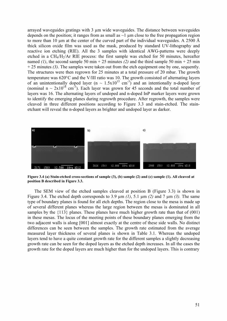
arrayed waveguides gratings with 3 µm wide waveguides. The distance between waveguides depends on the position; it ranges from as small as ~1 µm close to the free propagation region to more than 10 µm at the center of the curved part of the individual waveguides. A 2500 Å thick silicon oxide film was used as the mask, produced by standard UV-lithography and reactive ion etching (RIE). All the 3 samples with identical AWG-patterns were deeply etched in a CH4/H2/Ar RIE process: the first sample was etched for 50 minutes, hereafter named (1), the second sample 50 min + 25 minutes (2) and the third sample 50 min + 25 min + 25 minutes (3). The samples were taken out from the etch equipment one by one, sequently. The structures were then regrown for 25 minutes at a total pressure of 20 mbar. The growth temperature was 620°C and the V/III ratio was 10. The growth consisted of alternating layers of an unintentionally doped layer (n ~ 1.5x1015 cm-3) and an intentionally n-doped layer (nominal n ~ 2x1018 cm-3). Each layer was grown for 45 seconds and the total number of layers was 16. The alternating layers of undoped and n-doped InP marker layers were grown to identify the emerging planes during regrowth procedure. After regrowth, the samples were cleaved in three different positions according to Figure 3.3 and stain-etched. The stain-etchant will reveal the n-doped layers as brighter and undoped layer as darker.
Figure 3.4 (a) Stain-etched cross-sections of sample (3), (b) sample (2) and (c) sample (1). All cleaved at position B described in Figure 3.3.
The SEM view of the etched samples cleaved at position B (Figure 3.3) is shown in Figure 3.4. The etched depth corresponds to 3.9 µm (1), 5.1 µm (2) and 7 µm (3). The same type of boundary planes is found for all etch depths. The region close to the mesa is made up of several different planes whereas the large region between the mesas is dominated in all samples by the {113} planes. These planes have much higher growth rate than that of (001) in these mesas. The locus of the meeting points of these boundary planes emerging from the two adjacent walls is along [001] almost exactly at the centre of these side walls. No distinct differences can be seen between the samples. The growth rate estimated from the average measured layer thickness of several planes is shown in Table 3.1. Whereas the undoped layers tend to have a quite constant growth rate for the different samples a slightly decreasing growth rate can be seen for the doped layers as the etched depth increases. In all the cases the growth rate for the doped layers are much higher than for the undoped layers. This is contrary
51
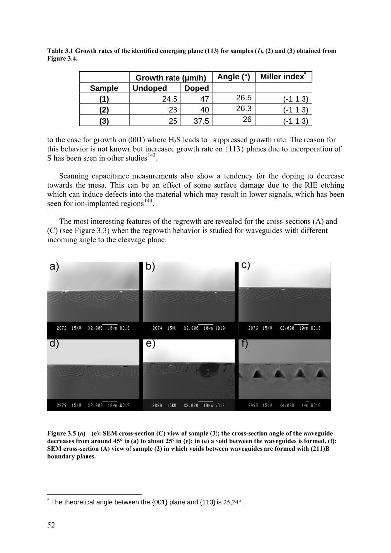
Table 3.1 Growth rates of the identified emerging plane (113) for samples (1), (2) and (3) obtained from Figure 3.4.
Growth rate (µm/h) Angle (°) Miller index*
Sample Undoped Doped (1) 24.5 47 26.5 (-1 1 3) (2) 23 40 26.3 (-1 1 3) (3) 25 37.5 26 (-1 1 3)
to the case for growth on (001) where H2S leads to suppressed growth rate. The reason for this behavior is not known but increased growth rate on {113} planes due to incorporation of S has been seen in other studies143. Scanning capacitance measurements also show a tendency for the doping to decrease towards the mesa. This can be an effect of some surface damage due to the RIE etching which can induce defects into the material which may result in lower signals, which has been seen for ion-implanted regions144.
The most interesting features of the regrowth are revealed for the cross-sections (A) and (C) (see Figure 3.3) when the regrowth behavior is studied for waveguides with different incoming angle to the cleavage plane.
Figure 3.5 (a) – (e): SEM cross-section (C) view of sample (3); the cross-section angle of the waveguide decreases from around 45° in (a) to about 25° in (e); in (e) a void between the waveguides is formed. (f): SEM cross-section (A) view of sample (2) in which voids between waveguides are formed with (211)B boundary planes. * The theoretical angle between the {001} plane and {113} is 25,24°.
52
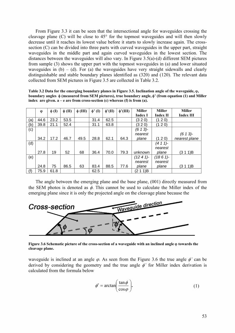
From Figure 3.3 it can be seen that the intersectional angle for waveguides crossing the cleavage plane (C) will be close to 45° for the topmost waveguides and will then slowly decrease until it reaches its lowest value before it starts to slowly increase again. The cross-section (C) can be divided into three parts with curved waveguides in the upper part, straight waveguides in the middle part and again curved waveguides in the lowest section. The distances between the waveguides will also vary. In Figure 3.5(a)-(d) different SEM pictures from sample (3) shows the upper part with the topmost waveguides in (a) and lower situated waveguides in (b) – (d). For (a) the waveguides have very straight sidewalls and clearly distinguishable and stable boundary planes identified as (320) and (120). The relevant data collected from SEM pictures in Figure 3.5 are collected in Table 3.2. Table 3.2 Data for the emerging boundary planes in Figure 3.5. Inclination angle of the waveguide, ϕ, boundary angles φ (measured from SEM pictures), true boundary angle, φ’ (from equation (1) and Miller index are given. a – e are from cross-section (c) whereas (f) is from (a). ϕ φ (I) φ (II) φ (III) φ’ (I) φ’(II) φ’(III) Miller
Index I Miller
Index II Miller
Index III (a) 44.6 23.2 53.5 31.4 62.5 (3 2 0) (1 2 0) (b) 39.8 21.1 52.4 31.1 63.8 (3 2 0) (1 2 0) (c)
34.2 17.2 46.7 49.5 28.8 62.1 64.3
(6 1 3)-nearest plane (1 2 0)
(6 1 3)- nearest plane
(d)
27.8 19 52 68 36.4 70.0 79.3 unknown
(4 1 1)-nearest plane (3 1 1)B
(e)
24.8 75 86.5 63 83.4 88.5 77.6
(12 4 1)- nearest plane
(18 6 1)-nearest plane (3 1 1)B
(f) 75.9 61.8 62.5 (2 1 1)B
The angle between the emerging plane and the base plane, (001) directly measured from the SEM photos is denoted as φ. This cannot be used to calculate the Miller index of the emerging plane since it is only the projected angle on the cleavage plane because the
Figure 3.6 Schematic picture of the cross-section of a waveguide with an inclined angle ϕ towards the cleavage plane. waveguide is inclined at an angle ϕ. As seen from the Figure 3.6 the true angle φ’ can be derived by considering the geometry and the true angle φ’ for Miller index derivation is calculated from the formula below
⎟⎟⎠
⎞⎜⎜⎝
⎛=′
ϕφφ
costanarctan . (1)
53
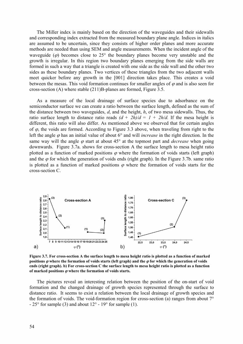
The Miller index is mainly based on the direction of the waveguides and their sidewalls and corresponding index extracted from the measured boundary plane angle. Indices in italics are assumed to be uncertain, since they consists of higher order planes and more accurate methods are needed than using SEM and angle measurements. When the incident angle of the waveguide (ϕ) becomes close to 25° the boundary planes become very unstable and the growth is irregular. In this region two boundary planes emerging from the side walls are formed in such a way that a triangle is created with one side as the side wall and the other two sides as these boundary planes. Two vertices of these triangles from the two adjacent walls meet quicker before any growth in the [001] direction takes place. This creates a void between the mesas. This void formation continues for smaller angles of ϕ and is also seen for cross-section (A) where stable (211)B-planes are formed, Figure 3.5.
As a measure of the local drainage of surface species due to adsorbance on the semiconductor surface we can create a ratio between the surface length, defined as the sum of the distance between two waveguides, d, and the height, h, of two mesa sidewalls. Thus, the ratio surface length to distance ratio reads (d + 2h)/d = 1 + 2h/d. If the mesa height is different, this ratio will also differ. As mentioned above we observed that for certain angles of ϕ, the voids are formed. According to Figure 3.3 above, when traveling from right to the left the angle ϕ has an initial value of about 6° and will increase in the right direction. In the same way will the angle ϕ start at about 45° at the topmost part and decrease when going downwards. Figure 3.7a. shows for cross-section A the surface length to mesa height ratio plotted as a function of marked positions ϕ where the formation of voids starts (left graph) and the ϕ for which the generation of voids ends (right graph). In the Figure 3.7b. same ratio is plotted as a function of marked positions ϕ where the formation of voids starts for the cross-section C.
Figure 3.7. For cross-section A the surface length to mesa height ratio is plotted as a function of marked positions ϕ where the formation of voids starts (left graph) and the ϕ for which the generation of voids ends (right graph). b) For cross-section C the surface length to mesa height ratio is plotted as a function of marked positions ϕ where the formation of voids starts.
The pictures reveal an interesting relation between the position of the on-start of void formation and the changed drainage of growth species represented through the surface to distance ratio. It seems to exist a relation between the local drainage of growth species and the formation of voids. The void-formation region for cross-section (a) ranges from about 7° - 25° for sample (3) and about 12° - 19° for sample (1).
54
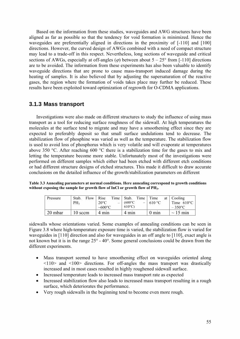
Based on the information from these studies, waveguides and AWG structures have been aligned as far as possible so that the tendency for void formation is minimized. Hence the waveguides are preferentially aligned in directions in the proximity of [-110] and [100] directions. However, the curved design of AWGs combined with a need of compact structure may lead to a trade-off in this respect. Nevertheless, long sections of waveguide and critical sections of AWGs, especially at off-angles (ϕ) between about 5 – 25° from [-110] directions are to be avoided. The information from these experiments has also been valuable to identify waveguide directions that are prone to cause mass-transport induced damage during the heating of samples. It is also believed that by adjusting the supersaturation of the reactive gases, the region where the formation of voids takes place may further be reduced. These results have been exploited toward optimization of regrowth for O-CDMA applications.
3.1.3 Mass transport Investigations were also made on different structures to study the influence of using mass transport as a tool for reducing surface roughness of the sidewall. At high temperatures the molecules at the surface tend to migrate and may have a smoothening effect since they are expected to preferably deposit so that small surface undulations tend to decrease. The stabilization flow of phosphine was varied as well as the temperature. The stabilization flow is used to avoid loss of phosphorus which is very volatile and will evaporate at temperatures above 350 °C. After reaching 600 °C there is a stabilization time for the gases to mix and letting the temperature become more stable. Unfortunately most of the investigations were performed on different samples which either had been etched with different etch conditions or had different structure designs of etched structures. This made it difficult to draw accurate conclusions on the detailed influence of the growth/stabilization parameters on different Table 3.3 Annealing parameters at normal conditions. Here annealing correspond to growth conditions without exposing the sample for growth flow of InCl or growth flow of PH3.
Pressure Stab. Flow PH3
Rise Time20°C – ~600°C
Stab. Time(600°C – 610°C)
Time at 610 °C
Cooling Time 610°C – 350°C
20 mbar 10 sccm 4 min 4 min 0 min ~ 15 min sidewalls whose orientations varied. Some examples of annealing conditions can be seen in Figure 3.8 where high-temperature exposure time is varied, the stabilization flow is varied for waveguides in [110] direction and also for waveguides in an off angle to [110], exact angle is not known but it is in the range 25° - 40°. Some general conclusions could be drawn from the different experiments.
• Mass transport seemed to have smoothening effect on waveguides oriented along <110> and <100> directions. For off-angles the mass transport was drastically increased and in most cases resulted in highly roughened sidewall surface.
• Increased temperature leads to increased mass transport rate as expected • Increased stabilization flow also leads to increased mass transport resulting in a rough
surface, which deteriorates the performance. • Very rough sidewalls in the beginning tend to become even more rough.
55
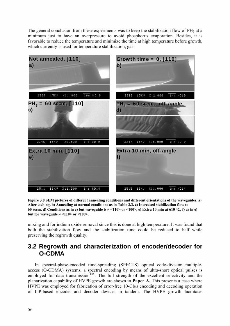
The general conclusion from these experiments was to keep the stabilization flow of PH3 at a minimum just to have an overpressure to avoid phosphorus evaporation. Besides, it is favorable to reduce the temperature and minimize the time at high temperature before growth, which currently is used for temperature stabilization, gas
Extra 10 min, offExtra 10 min, off--angleanglef)f)
Growth time = 0, [110]Growth time = 0, [110]b)b)
Not annealed, [110]Not annealed, [110]a)a)
PHPH33 = 60 sccm, [110]= 60 sccm, [110]c)c)
PHPH33 = 60 sccm, off= 60 sccm, off--angleangled)d)
Extra 10 min, [110]Extra 10 min, [110]e)e)
Extra 10 min, offExtra 10 min, off--angleanglef)f)
Growth time = 0, [110]Growth time = 0, [110]b)b)
Not annealed, [110]Not annealed, [110]a)a)
PHPH33 = 60 sccm, [110]= 60 sccm, [110]c)c)
PHPH33 = 60 sccm, off= 60 sccm, off--angleangled)d)
Extra 10 min, [110]Extra 10 min, [110]e)e)
Figure 3.8 SEM pictures of different annealing conditions and different orientations of the waveguides. a) After etching. b) Annealing at normal conditions as in Table 3.3. c) Increased stabilization flow to 60 sccm. d) Conditions as in c) but waveguide is ≠ <110> or <100>, e) Extra 10 min at 610 °C, f) as in e) but for waveguide ≠ <110> or <100>. mixing and for indium oxide removal since this is done at high temperature. It was found that both the stabilization flow and the stabilization time could be reduced to half while preserving the regrowth quality.
3.2 Regrowth and characterization of encoder/decoder for O-CDMA
In spectral-phase-encoded time-spreading (SPECTS) optical code-division multiple-access (O-CDMA) systems, a spectral encoding by means of ultra-short optical pulses is employed for data transmission145. The full strength of the excellent selectivity and the planarization capability of HVPE growth are shown in Paper A. This presents a case where HVPE was employed for fabrication of error-free 10-Gb/s encoding and decoding operation of InP-based encoder and decoder devices in tandem. The HVPE growth facilitates
56
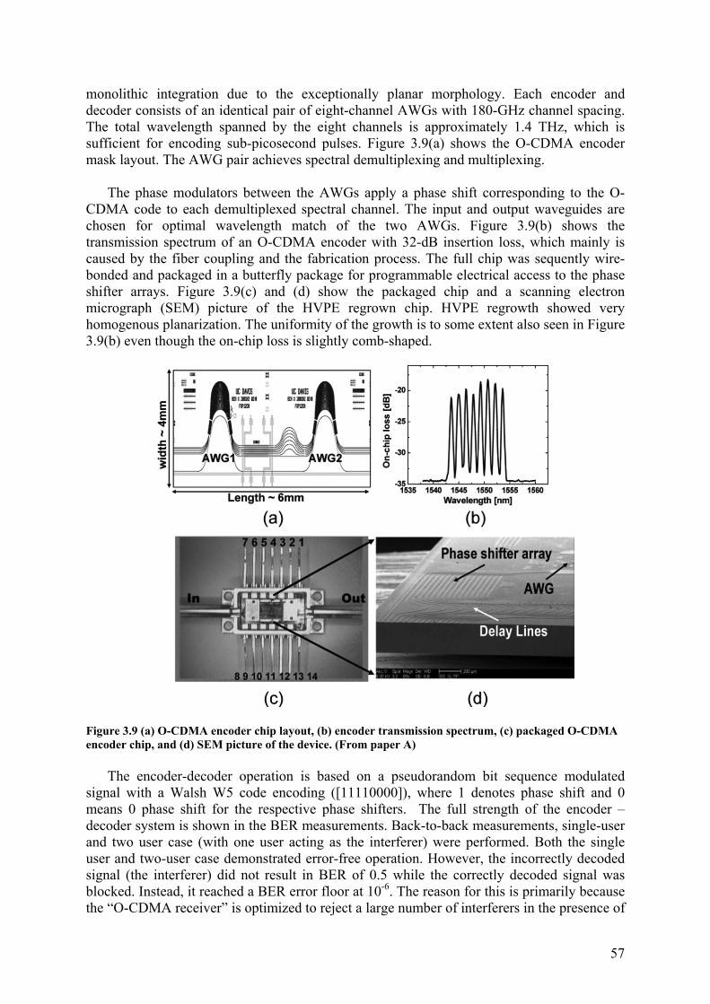
monolithic integration due to the exceptionally planar morphology. Each encoder and decoder consists of an identical pair of eight-channel AWGs with 180-GHz channel spacing. The total wavelength spanned by the eight channels is approximately 1.4 THz, which is sufficient for encoding sub-picosecond pulses. Figure 3.9(a) shows the O-CDMA encoder mask layout. The AWG pair achieves spectral demultiplexing and multiplexing.
The phase modulators between the AWGs apply a phase shift corresponding to the O-CDMA code to each demultiplexed spectral channel. The input and output waveguides are chosen for optimal wavelength match of the two AWGs. Figure 3.9(b) shows the transmission spectrum of an O-CDMA encoder with 32-dB insertion loss, which mainly is caused by the fiber coupling and the fabrication process. The full chip was sequently wire-bonded and packaged in a butterfly package for programmable electrical access to the phase shifter arrays. Figure 3.9(c) and (d) show the packaged chip and a scanning electron micrograph (SEM) picture of the HVPE regrown chip. HVPE regrowth showed very homogenous planarization. The uniformity of the growth is to some extent also seen in Figure 3.9(b) even though the on-chip loss is slightly comb-shaped.
Figure 3.9 (a) O-CDMA encoder chip layout, (b) encoder transmission spectrum, (c) packaged O-CDMA encoder chip, and (d) SEM picture of the device. (From paper A) The encoder-decoder operation is based on a pseudorandom bit sequence modulated signal with a Walsh W5 code encoding ([11110000]), where 1 denotes phase shift and 0 means 0 phase shift for the respective phase shifters. The full strength of the encoder – decoder system is shown in the BER measurements. Back-to-back measurements, single-user and two user case (with one user acting as the interferer) were performed. Both the single user and two-user case demonstrated error-free operation. However, the incorrectly decoded signal (the interferer) did not result in BER of 0.5 while the correctly decoded signal was blocked. Instead, it reached a BER error floor at 10-6. The reason for this is primarily because the “O-CDMA receiver” is optimized to reject a large number of interferers in the presence of
57
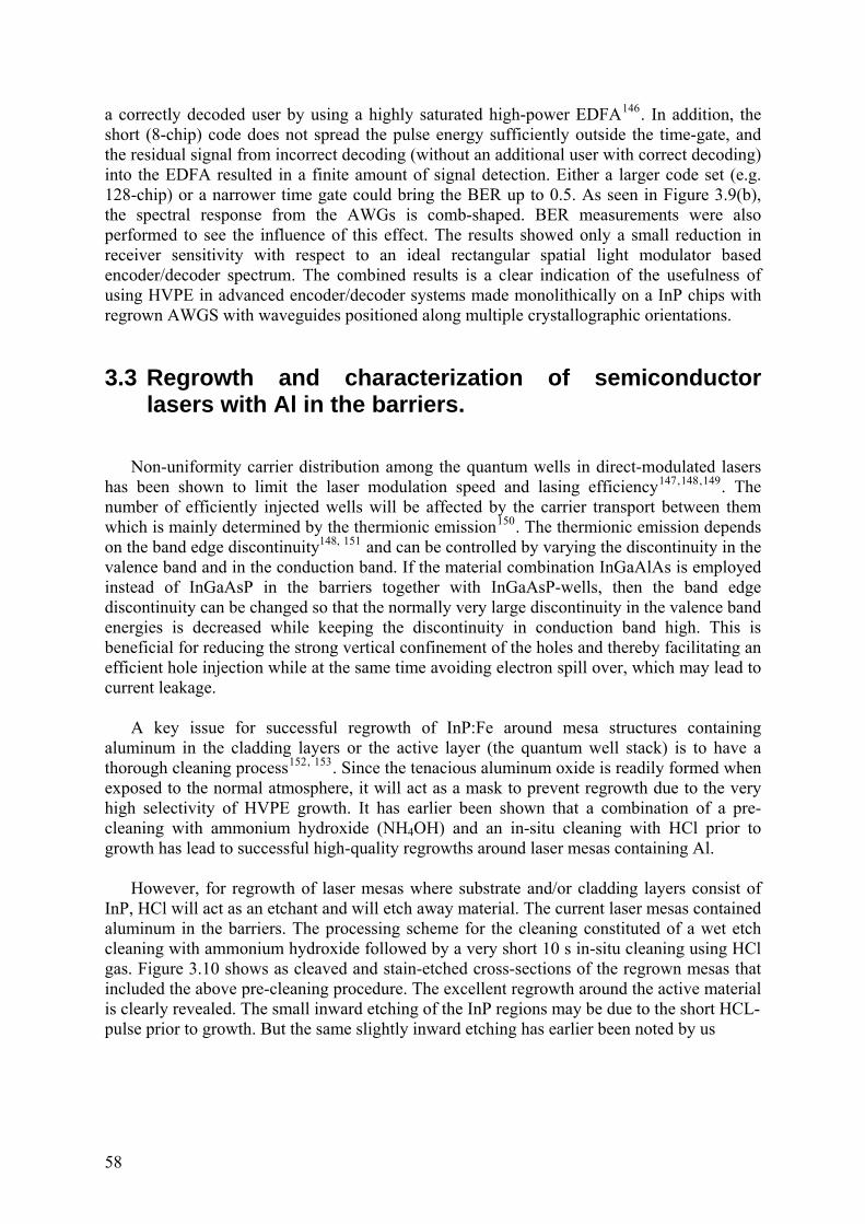
a correctly decoded user by using a highly saturated high-power EDFA146. In addition, the short (8-chip) code does not spread the pulse energy sufficiently outside the time-gate, and the residual signal from incorrect decoding (without an additional user with correct decoding) into the EDFA resulted in a finite amount of signal detection. Either a larger code set (e.g. 128-chip) or a narrower time gate could bring the BER up to 0.5. As seen in Figure 3.9(b), the spectral response from the AWGs is comb-shaped. BER measurements were also performed to see the influence of this effect. The results showed only a small reduction in receiver sensitivity with respect to an ideal rectangular spatial light modulator based encoder/decoder spectrum. The combined results is a clear indication of the usefulness of using HVPE in advanced encoder/decoder systems made monolithically on a InP chips with regrown AWGS with waveguides positioned along multiple crystallographic orientations.
3.3 Regrowth and characterization of semiconductor lasers with Al in the barriers.
Non-uniformity carrier distribution among the quantum wells in direct-modulated lasers has been shown to limit the laser modulation speed and lasing efficiency147, ,148 149. The number of efficiently injected wells will be affected by the carrier transport between them which is mainly determined by the thermionic emission150. The thermionic emission depends on the band edge discontinuity148, 151 and can be controlled by varying the discontinuity in the valence band and in the conduction band. If the material combination InGaAlAs is employed instead of InGaAsP in the barriers together with InGaAsP-wells, then the band edge discontinuity can be changed so that the normally very large discontinuity in the valence band energies is decreased while keeping the discontinuity in conduction band high. This is beneficial for reducing the strong vertical confinement of the holes and thereby facilitating an efficient hole injection while at the same time avoiding electron spill over, which may lead to current leakage.
A key issue for successful regrowth of InP:Fe around mesa structures containing aluminum in the cladding layers or the active layer (the quantum well stack) is to have a thorough cleaning process152, 153. Since the tenacious aluminum oxide is readily formed when exposed to the normal atmosphere, it will act as a mask to prevent regrowth due to the very high selectivity of HVPE growth. It has earlier been shown that a combination of a pre-cleaning with ammonium hydroxide (NH4OH) and an in-situ cleaning with HCl prior to growth has lead to successful high-quality regrowths around laser mesas containing Al.
However, for regrowth of laser mesas where substrate and/or cladding layers consist of InP, HCl will act as an etchant and will etch away material. The current laser mesas contained aluminum in the barriers. The processing scheme for the cleaning constituted of a wet etch cleaning with ammonium hydroxide followed by a very short 10 s in-situ cleaning using HCl gas. Figure 3.10 shows as cleaved and stain-etched cross-sections of the regrown mesas that included the above pre-cleaning procedure. The excellent regrowth around the active material is clearly revealed. The small inward etching of the InP regions may be due to the short HCL- pulse prior to growth. But the same slightly inward etching has earlier been noted by us
58
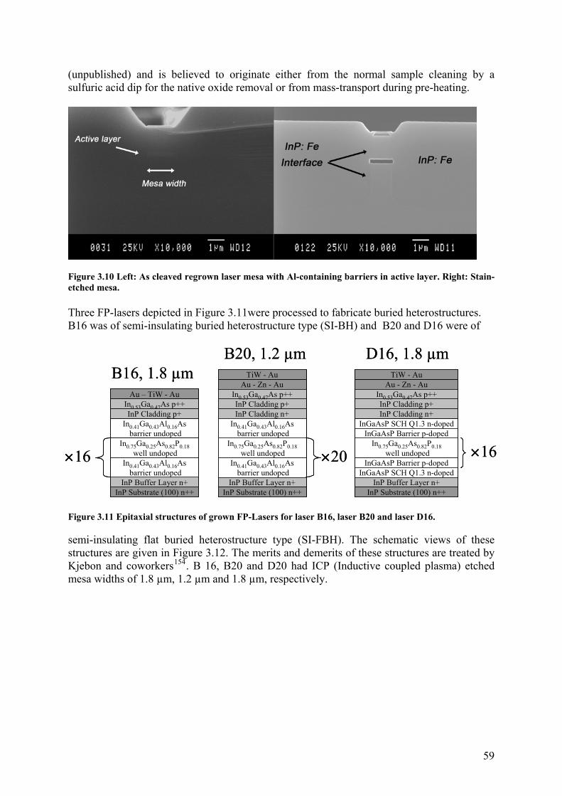
(unpublished) and is believed to originate either from the normal sample cleaning by a sulfuric acid dip for the native oxide removal or from mass-transport during pre-heating.
Figure 3.10 Left: As cleaved regrown laser mesa with Al-containing barriers in active layer. Right: Stain-etched mesa. Three FP-lasers depicted in Figure 3.11were processed to fabricate buried heterostructures. B16 was of semi-insulating buried heterostructure type (SI-BH) and B20 and D16 were of
InP Substrate (100) n++InP Buffer Layer n+
Au – TiW - Au
InP Buffer Layer n+InP Substrate (100) n++
In0.41Ga0.43Al0.16Asbarrier undoped
In0.75Ga0.25As0.82P0.18well undoped
InGaAsP Barrier p-doped
In0.41Ga0.43Al0.16Asbarrier undoped
InGaAsP SCH Q1.3 n-doped
In0.75Ga0.25As0.82P0.18well undoped
InGaAsP SCH Q1.3 n-dopedInGaAsP Barrier p-doped
InP Cladding n+InP Cladding p+In0.53Ga0.47As p++
InP Cladding p+
In0.53Ga0.47As p++
InP Cladding n+InP Cladding p+
In0.53Ga0.47As p++Au - Zn - Au
TiW - AuAu - Zn - Au
TiW - Au
In0.41Ga0.43Al0.16Asbarrier undoped
×16×20×16In0.75Ga0.25As0.82P0.18
well undopedIn0.41Ga0.43Al0.16As
barrier undopedInP Buffer Layer n+
InP Substrate (100) n++
B16, 1.8 µmD16, 1.8 µmB20, 1.2 µm
Figure 3.11 Epitaxial structures of grown FP-Lasers for laser B16, laser B20 and laser D16. semi-insulating flat buried heterostructure type (SI-FBH). The schematic views of these structures are given in Figure 3.12. The merits and demerits of these structures are treated by Kjebon and coworkers154. B 16, B20 and D20 had ICP (Inductive coupled plasma) etched mesa widths of 1.8 µm, 1.2 µm and 1.8 µm, respectively.
59
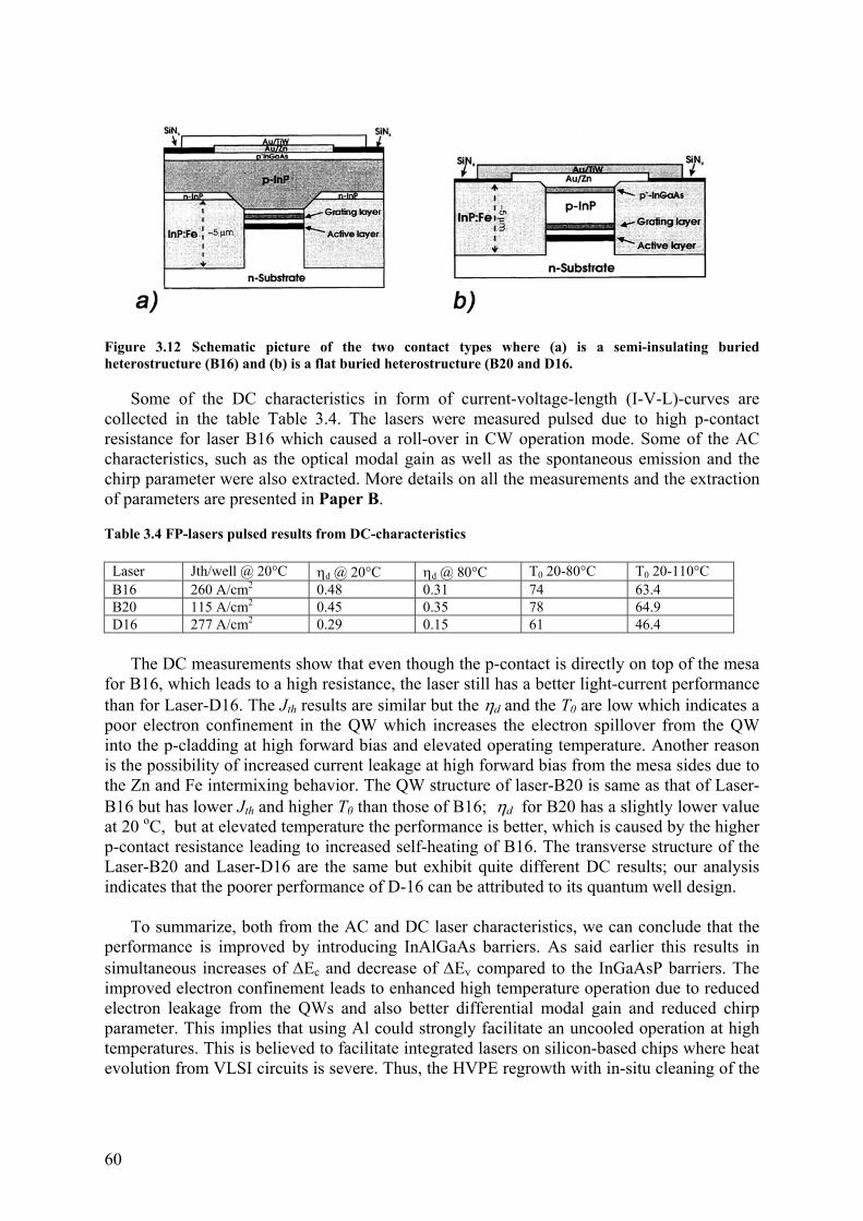
Figure 3.12 Schematic picture of the two contact types where (a) is a semi-insulating buried heterostructure (B16) and (b) is a flat buried heterostructure (B20 and D16.
Some of the DC characteristics in form of current-voltage-length (I-V-L)-curves are collected in the table Table 3.4. The lasers were measured pulsed due to high p-contact resistance for laser B16 which caused a roll-over in CW operation mode. Some of the AC characteristics, such as the optical modal gain as well as the spontaneous emission and the chirp parameter were also extracted. More details on all the measurements and the extraction of parameters are presented in Paper B. Table 3.4 FP-lasers pulsed results from DC-characteristics
Laser Jth/well @ 20°C ηd @ 20°C ηd @ 80°C T0 20-80°C T0 20-110°C B16 260 A/cm2 0.48 0.31 74 63.4 B20 115 A/cm2 0.45 0.35 78 64.9 D16 277 A/cm2 0.29 0.15 61 46.4
The DC measurements show that even though the p-contact is directly on top of the mesa for B16, which leads to a high resistance, the laser still has a better light-current performance than for Laser-D16. The Jth results are similar but the ηd and the T0 are low which indicates a poor electron confinement in the QW which increases the electron spillover from the QW into the p-cladding at high forward bias and elevated operating temperature. Another reason is the possibility of increased current leakage at high forward bias from the mesa sides due to the Zn and Fe intermixing behavior. The QW structure of laser-B20 is same as that of Laser-B16 but has lower Jth and higher T0 than those of B16; ηd for B20 has a slightly lower value at 20 oC, but at elevated temperature the performance is better, which is caused by the higher p-contact resistance leading to increased self-heating of B16. The transverse structure of the Laser-B20 and Laser-D16 are the same but exhibit quite different DC results; our analysis indicates that the poorer performance of D-16 can be attributed to its quantum well design.
To summarize, both from the AC and DC laser characteristics, we can conclude that the performance is improved by introducing InAlGaAs barriers. As said earlier this results in simultaneous increases of ΔEc and decrease of ΔEv compared to the InGaAsP barriers. The improved electron confinement leads to enhanced high temperature operation due to reduced electron leakage from the QWs and also better differential modal gain and reduced chirp parameter. This implies that using Al could strongly facilitate an uncooled operation at high temperatures. This is believed to facilitate integrated lasers on silicon-based chips where heat evolution from VLSI circuits is severe. Thus, the HVPE regrowth with in-situ cleaning of the
60
Al-containing structures seem to be offer an excellent opportunity for manufacturing such devices.
3.4 Large mask area effects in selective epitaxy
In microelectronics and optoelectronics, many applications rely on the possibility of achieving selective epitaxy or selective area growth (SAG). A good understanding on growth rates caused by the mask area/open area and concentration of the active species is essential. This includes the detailed knowledge on the gas phase diffusion coefficients (D) for different precursors and reaction rate constants (k) since these can lead to compositional changes of ternary or quaternary materials in SAG155.
Most existing models deal with cases where the pattern fields consist of smaller masked areas than open areas; besides in such studies, these areas separated from each other. We undertook a study on patterns consisting of larger masked areas than open areas; in our study the open areas are surrounded by the larger mask areas in all directions. This is a situation where many 2-dimensional models often fail to explain the experimental data and more sophisticated models tend to be too complicated in addition to heavy computational demand. The case with a large ratio of mask area to the opening area is faced commonly when it comes to epitaxial lateral overgrowth and better knowledge of growth modes can help in designing more effective masks with optimized patterns. Paper C handles modeling of the case where the large mask areas will affect the growth properties in selective epitaxy.
Samples may have a mask pattern of type dark-field (DF), i.e., the major part of the
substrate is covered by a mask and only small areas has exposed semiconductor surface or they may have a mask pattern which of type light-field (LF) and whose pattern mainly consisted of large open semiconductor surface with only minor areas covered by mask.
The influence of the kinetic and the transport effects can be studied by applying a SAG thin-film analytical model. However, when applied on samples with LF patterns and on DF patterns it was found for the DF pattern that the efficiency formula in the model fails to account for all the extra supply of growth rendering species from the longitudinal direction [110] from the masked regions surround the longitudinal edges, thus transport of species from all the three dimensions has to be considered. In the LF case a one dimensional filling factor (θ1d) was used which is defined as the ratio of the opening width (Ow) to the sum of the opening width and the mask width (Mw) but in the DF case the filling factor needed to be extended into two dimensions In doing so, the thin-film model was extended to include two-dimensional filling factors, θ2d, and to use the normalized growth volume instead of the normalized cross-sectional area as a measure of the efficiency. The extended 2-dimensional filling factor uses an area like the one below:
61
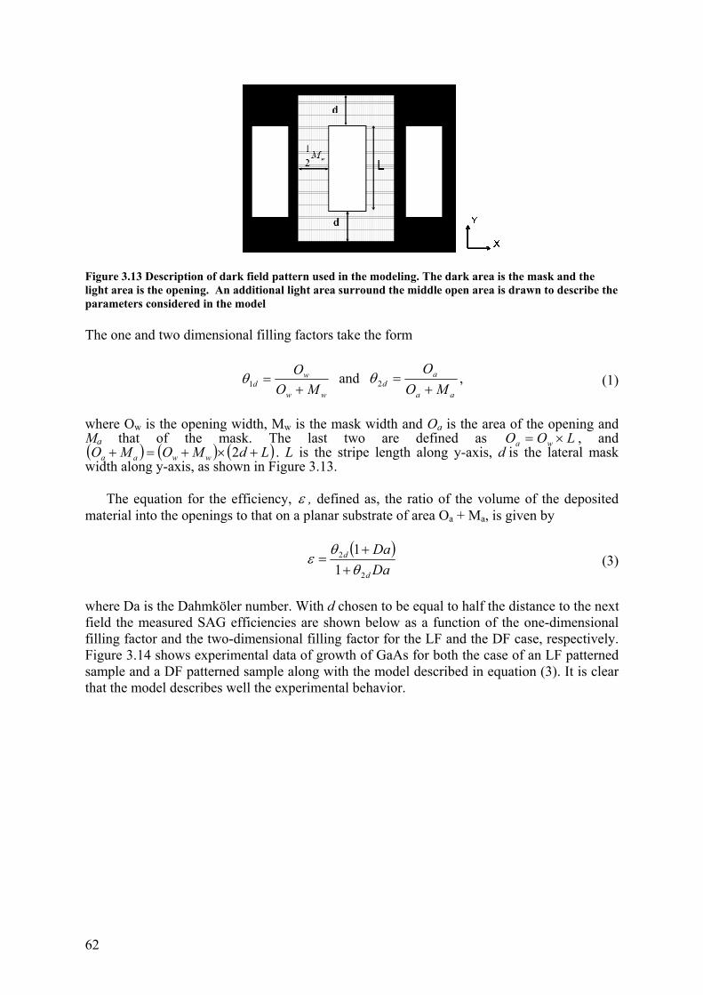
Figure 3.13 Description of dark field pattern used in the modeling. The dark area is the mask and the light area is the opening. An additional light area surround the middle open area is drawn to describe the parameters considered in the model The one and two dimensional filling factors take the form
ww
wd MO
O+
=1θ and aa
ad MO
O+
=2θ , (1)
where Ow is the opening width, Mw is the mask width and Oa is the area of the opening and M that of the mask. The last two are defined as wa , and
wwaa . L is the stripe length along y-axis, d is the lateral mask width along y-axis, as shown in Figure 3.13.
a LOO ×=( ) ( ) ( )LdMOMO +×+=+ 2
The equation for the efficiency, ε , defined as, the ratio of the volume of the deposited material into the openings to that on a planar substrate of area Oa + Ma, is given by
( )
DaDa
d
d
2
2
11θ
θε
++
= (3)
where Da is the Dahmköler number. With d chosen to be equal to half the distance to the next field the measured SAG efficiencies are shown below as a function of the one-dimensional filling factor and the two-dimensional filling factor for the LF and the DF case, respectively. Figure 3.14 shows experimental data of growth of GaAs for both the case of an LF patterned sample and a DF patterned sample along with the model described in equation (3). It is clear that the model describes well the experimental behavior.
62
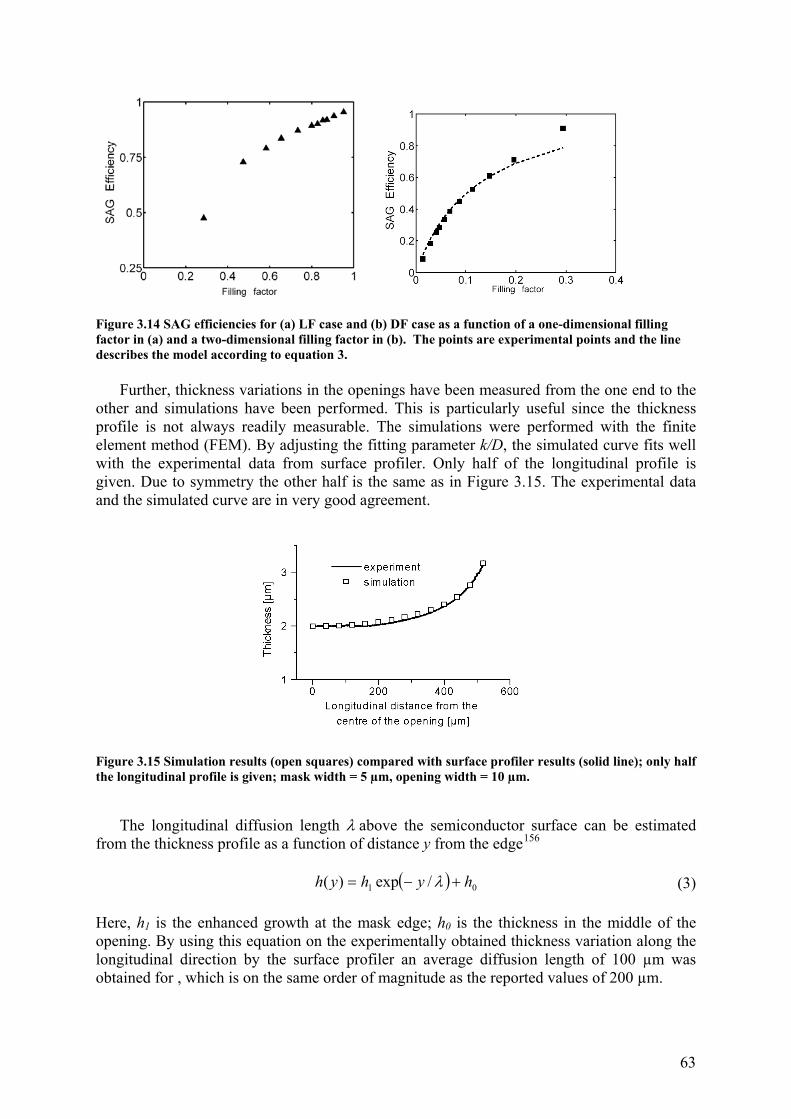
Figure 3.14 SAG efficiencies for (a) LF case and (b) DF case as a function of a one-dimensional filling factor in (a) and a two-dimensional filling factor in (b). The points are experimental points and the line describes the model according to equation 3.
Further, thickness variations in the openings have been measured from the one end to the other and simulations have been performed. This is particularly useful since the thickness profile is not always readily measurable. The simulations were performed with the finite element method (FEM). By adjusting the fitting parameter k/D, the simulated curve fits well with the experimental data from surface profiler. Only half of the longitudinal profile is given. Due to symmetry the other half is the same as in Figure 3.15. The experimental data and the simulated curve are in very good agreement.
Figure 3.15 Simulation results (open squares) compared with surface profiler results (solid line); only half the longitudinal profile is given; mask width = 5 µm, opening width = 10 µm.
The longitudinal diffusion length λ above the semiconductor surface can be estimated from the thickness profile as a function of distance y from the edge156
( ) 01 /exp)( hyhyh +−= λ (3)
Here, h1 is the enhanced growth at the mask edge; h0 is the thickness in the middle of the opening. By using this equation on the experimentally obtained thickness variation along the longitudinal direction by the surface profiler an average diffusion length of 100 µm was obtained for , which is on the same order of magnitude as the reported values of 200 µm.
63
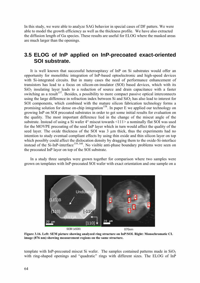
In this study, we were able to analyze SAG behavior in special cases of DF patters. We were able to model the growth efficiency as well as the thickness profile. We have also extracted the diffusion length of Ga species. These results are useful for ELOG where the masked areas are much larger than the openings.
3.5 ELOG of InP applied on InP-precoated exact-oriented SOI substrate.
It is well known that successful heteroepitaxy of InP on Si substrates would offer an opportunity for monolithic integration of InP-based optoelectronic and high-speed devices with Si-integrated circuits. But in many cases the need of performance enhancement of transistors has lead to a focus on silicon-on-insulator (SOI) based devices, which with its SiO2 insulating layer leads to a reduction of source and drain capacitance with a faster switching as a result157. Besides, a possibility to more compact passive optical interconnects using the large difference in refraction index between Si and SiO2 has also lead to interest for SOI components, which combined with the mature silicon fabrication technology forms a promising solution for dense on-chip integration158. In paper E we applied our technology on growing InP on SOI precoated substrates in order to get some initial results for evaluation on the quality. The most important difference lied in the change of the miscut angle of the substrate. Instead of using a Si wafer 4° miscut towards <111> a nominally flat SOI was used for the MOVPE precoating of the seed InP layer which in turn would affect the quality of the seed layer. The oxide thickness of the SOI was 3 µm thick, thus the experiments had no intention to study eventual compliant effects by using thin oxide and thin silicon layer on top which possibly could affect the dislocation density by dragging them to the oxide-Si-interface instead of the Si-InP-interface159,160. No visible anti-phase boundary problems were seen on the precoated InP layer on top of the SOI substrate. In a study three samples were grown together for comparison where two samples were grown on templates with InP-precoated SOI wafer with exact orientation and one sample on a
{110}
{111}B
{111}A
Undulation
[110]
[-110]{110}
{111}B
{111}A
Undulation
[110]
[-110]
Figure 3.16. Left: SEM picture showing analyzed ring structure on InP/SOI. Right: Monochromatic CL image (876 nm) showing measurement regions on the same structure.
template with InP-precoated miscut Si wafer. The samples contained patterns made in SiO2 with ring-shaped openings and “quadratic” rings with different sizes. The ELOG of InP
64
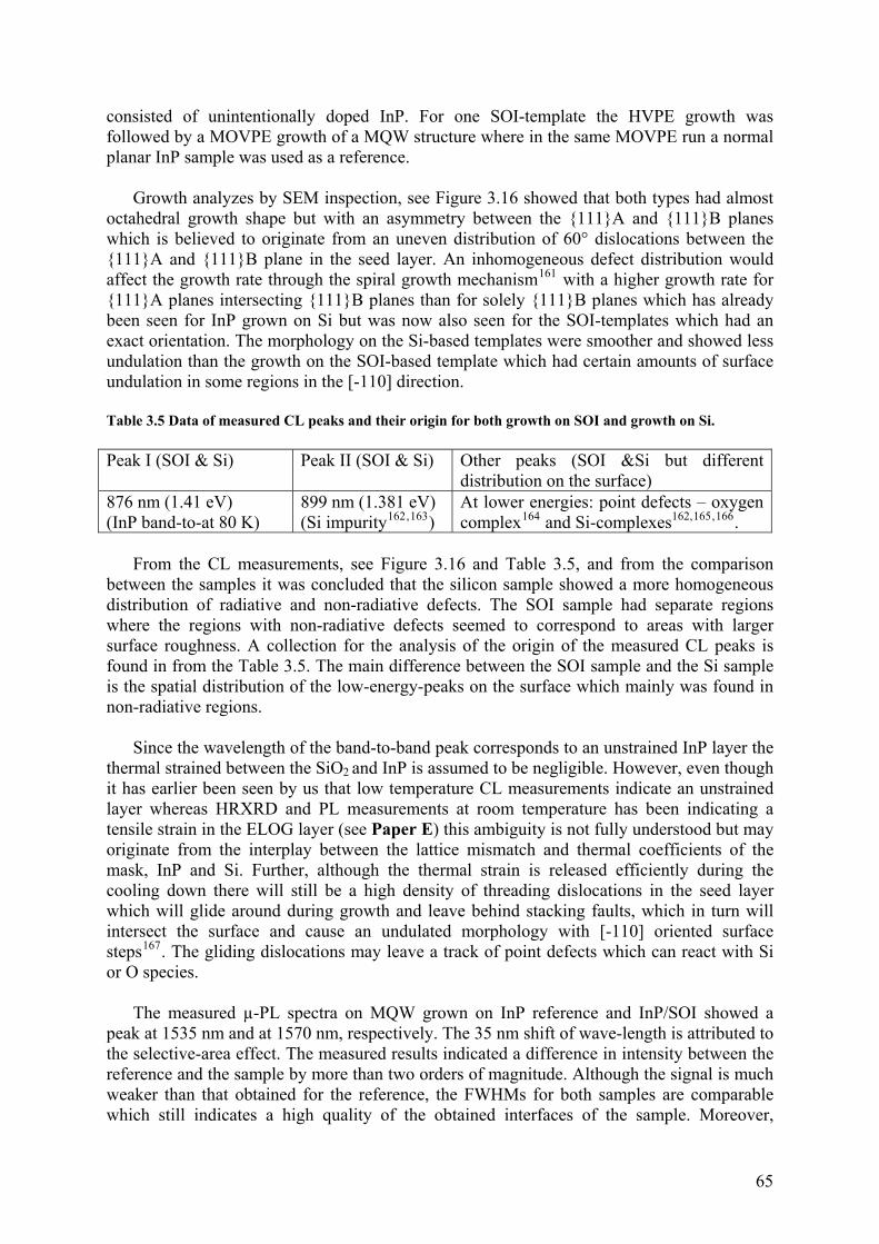
consisted of unintentionally doped InP. For one SOI-template the HVPE growth was followed by a MOVPE growth of a MQW structure where in the same MOVPE run a normal planar InP sample was used as a reference.
Growth analyzes by SEM inspection, see Figure 3.16 showed that both types had almost octahedral growth shape but with an asymmetry between the {111}A and {111}B planes which is believed to originate from an uneven distribution of 60° dislocations between the {111}A and {111}B plane in the seed layer. An inhomogeneous defect distribution would affect the growth rate through the spiral growth mechanism161 with a higher growth rate for {111}A planes intersecting {111}B planes than for solely {111}B planes which has already been seen for InP grown on Si but was now also seen for the SOI-templates which had an exact orientation. The morphology on the Si-based templates were smoother and showed less undulation than the growth on the SOI-based template which had certain amounts of surface undulation in some regions in the [-110] direction. Table 3.5 Data of measured CL peaks and their origin for both growth on SOI and growth on Si. Peak I (SOI & Si) Peak II (SOI & Si) Other peaks (SOI &Si but different
distribution on the surface) 876 nm (1.41 eV) (InP band-to-at 80 K)
899 nm (1.381 eV) (Si impurity162,163)
At lower energies: point defects – oxygen complex164 and Si-complexes162, ,165 166.
From the CL measurements, see Figure 3.16 and Table 3.5, and from the comparison
between the samples it was concluded that the silicon sample showed a more homogeneous distribution of radiative and non-radiative defects. The SOI sample had separate regions where the regions with non-radiative defects seemed to correspond to areas with larger surface roughness. A collection for the analysis of the origin of the measured CL peaks is found in from the Table 3.5. The main difference between the SOI sample and the Si sample is the spatial distribution of the low-energy-peaks on the surface which mainly was found in non-radiative regions.
Since the wavelength of the band-to-band peak corresponds to an unstrained InP layer the thermal strained between the SiO2 and InP is assumed to be negligible. However, even though it has earlier been seen by us that low temperature CL measurements indicate an unstrained layer whereas HRXRD and PL measurements at room temperature has been indicating a tensile strain in the ELOG layer (see Paper E) this ambiguity is not fully understood but may originate from the interplay between the lattice mismatch and thermal coefficients of the mask, InP and Si. Further, although the thermal strain is released efficiently during the cooling down there will still be a high density of threading dislocations in the seed layer which will glide around during growth and leave behind stacking faults, which in turn will intersect the surface and cause an undulated morphology with [-110] oriented surface steps167. The gliding dislocations may leave a track of point defects which can react with Si or O species.
The measured µ-PL spectra on MQW grown on InP reference and InP/SOI showed a peak at 1535 nm and at 1570 nm, respectively. The 35 nm shift of wave-length is attributed to the selective-area effect. The measured results indicated a difference in intensity between the reference and the sample by more than two orders of magnitude. Although the signal is much weaker than that obtained for the reference, the FWHMs for both samples are comparable which still indicates a high quality of the obtained interfaces of the sample. Moreover,
65
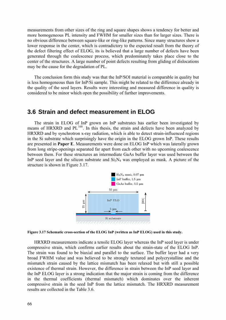
measurements from other sizes of the ring and square shapes shows a tendency for better and more homogeneous PL intensity and FWHM for smaller sizes than for larger sizes. There is no obvious difference between square-like or ring-like patterns. Since many structures show a lower response in the center, which is contradictory to the expected result from the theory of the defect filtering effect of ELOG, its is believed that a large number of defects have been generated through the coalescence process, which predominately takes place close to the center of the structures. A large number of point defects resulting from gliding of dislocations may be the cause for the degradation of PL. The conclusion form this study was that the InP/SOI material is comparable in quality but is less homogeneous than for InP/Si sample. This might be related to the difference already in the quality of the seed layers. Results were interesting and measured difference in quality is considered to be minor which open the possibility of further improvements.
3.6 Strain and defect measurement in ELOG The strain in ELOG of InP grown on InP substrates has earlier been investigated by
means of HRXRD and PL168. In this thesis, the strain and defects have been analyzed by HRXRD and by synchrotron x-ray radiation, which is able to detect strain-influenced regions in the Si substrate which surprisingly have the origin in the ELOG grown InP. These results are presented in Paper E. Measurements were done on ELOG InP which was laterally grown from long stripe-openings separated far apart from each other with no upcoming coalescence between them. For these structures an intermediate GaAs buffer layer was used between the InP seed layer and the silicon substrate and Si3N4 was employed as mask. A picture of the structure is shown in Figure 3.17.
Figure 3.17 Schematic cross-section of the ELOG InP (written as InP ELOG) used in this study.
HRXRD measurements indicate a tensile ELOG layer whereas the InP seed layer is under compressive strain, which confirms earlier results about the strain-state of the ELOG InP. The strain was found to be biaxial and parallel to the surface. The buffer layer had a very broad FWHM value and was believed to be strongly textured and polycrystalline and the mismatch strain caused by the lattice mismatch has been relaxed but with still a possible existence of thermal strain. However, the difference in strain between the InP seed layer and the InP ELOG layer is a strong indication that the major strain is coming from the difference in the thermal coefficients (thermal mismatch) which dominates over the inherent compressive strain in the seed InP from the lattice mismatch. The HRXRD measurement results are collected in the Table 3.6.
66
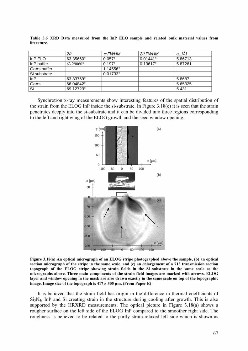
Table 3.6 XRD Data measured from the InP ELO sample and related bulk material values from literature. 2θ ϖ FWHM 2θ FWHM a⊥ [Å] InP ELO 63.35660° 0.057° 0.01441° 5.86713 InP buffer 63.29060° 0.197° 0.13617° 5.87261 GaAs buffer 1.14556° Si substrate 0.01733° InP 63.33769° 5.8687 GaAs 66.04842° 5.65325 Si 69.12723° 5.431
Synchrotron x-ray measurements show interesting features of the spatial distribution of the strain from the ELOG InP inside the si-substrate. In Figure 3.18(c) it is seen that the strain penetrates deeply into the si-substrate and it can be divided into three regions corresponding to the left and right wing of the ELOG growth and the seed window opening.
Figure 3.18(a) An optical micrograph of an ELOG stripe photographed above the sample, (b) an optical section micrograph of the stripe in the same scale, and (c) an enlargement of a 713 transmission section topograph of the ELOG stripe showing strain fields in the Si substrate in the same scale as the micrographs above. Three main components of the strain field images are marked with arrows. ELOG layer and window opening in the mask are also drawn exactly in the same scale on top of the topographic image. Image size of the topograph is 417 × 305 µm. (From Paper E) It is believed that the strain field has origin in the difference in thermal coefficients of Si3N4, InP and Si creating strain in the structure during cooling after growth. This is also supported by the HRXRD measurements. The optical picture in Figure 3.18(a) shows a rougher surface on the left side of the ELOG InP compared to the smoother right side. The roughness is believed to be related to the partly strain-relaxed left side which is shown as
67
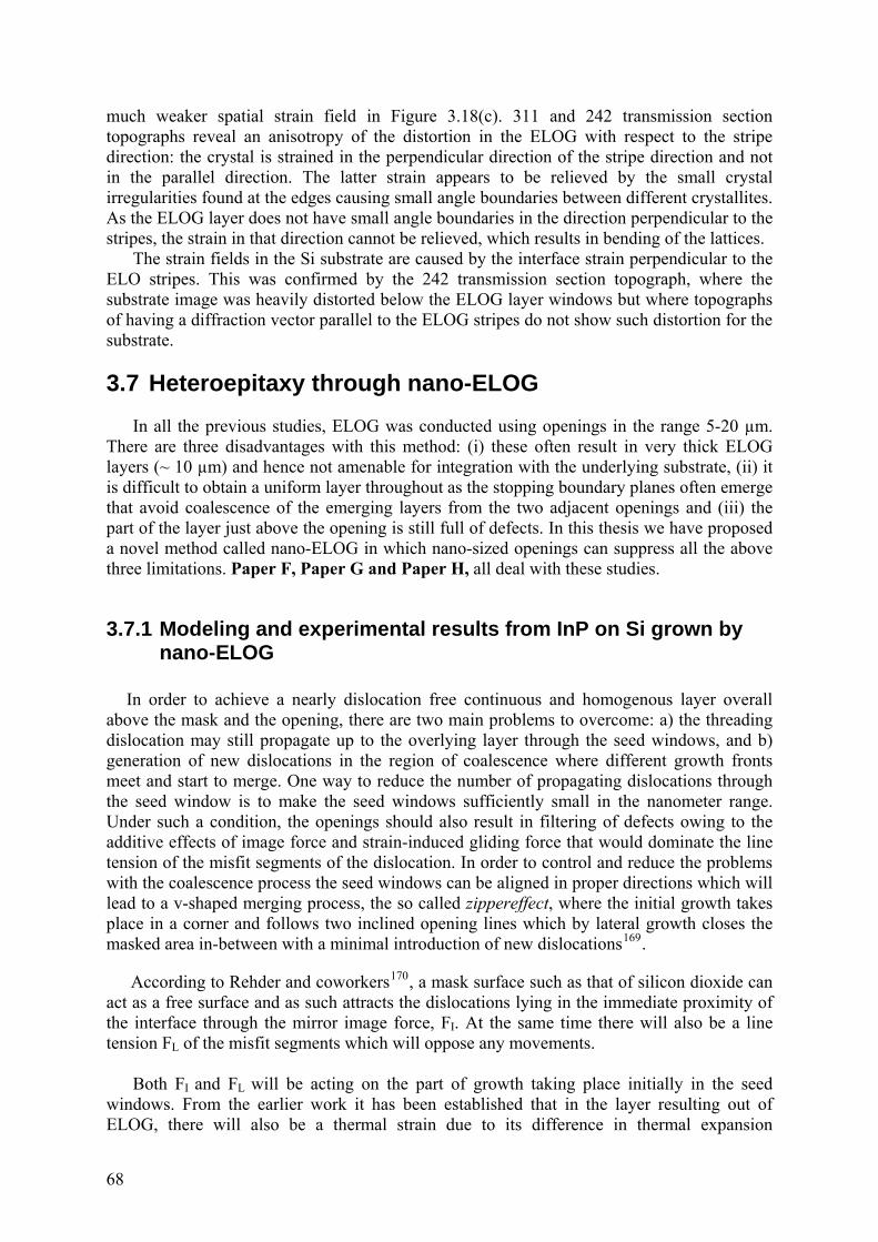
much weaker spatial strain field in Figure 3.18(c). 311 and 242 transmission section topographs reveal an anisotropy of the distortion in the ELOG with respect to the stripe direction: the crystal is strained in the perpendicular direction of the stripe direction and not in the parallel direction. The latter strain appears to be relieved by the small crystal irregularities found at the edges causing small angle boundaries between different crystallites. As the ELOG layer does not have small angle boundaries in the direction perpendicular to the stripes, the strain in that direction cannot be relieved, which results in bending of the lattices. The strain fields in the Si substrate are caused by the interface strain perpendicular to the ELO stripes. This was confirmed by the 242 transmission section topograph, where the substrate image was heavily distorted below the ELOG layer windows but where topographs of having a diffraction vector parallel to the ELOG stripes do not show such distortion for the substrate.
3.7 Heteroepitaxy through nano-ELOG In all the previous studies, ELOG was conducted using openings in the range 5-20 µm.
There are three disadvantages with this method: (i) these often result in very thick ELOG layers (~ 10 µm) and hence not amenable for integration with the underlying substrate, (ii) it is difficult to obtain a uniform layer throughout as the stopping boundary planes often emerge that avoid coalescence of the emerging layers from the two adjacent openings and (iii) the part of the layer just above the opening is still full of defects. In this thesis we have proposed a novel method called nano-ELOG in which nano-sized openings can suppress all the above three limitations. Paper F, Paper G and Paper H, all deal with these studies.
3.7.1 Modeling and experimental results from InP on Si grown by nano-ELOG
In order to achieve a nearly dislocation free continuous and homogenous layer overall above the mask and the opening, there are two main problems to overcome: a) the threading dislocation may still propagate up to the overlying layer through the seed windows, and b) generation of new dislocations in the region of coalescence where different growth fronts meet and start to merge. One way to reduce the number of propagating dislocations through the seed window is to make the seed windows sufficiently small in the nanometer range. Under such a condition, the openings should also result in filtering of defects owing to the additive effects of image force and strain-induced gliding force that would dominate the line tension of the misfit segments of the dislocation. In order to control and reduce the problems with the coalescence process the seed windows can be aligned in proper directions which will lead to a v-shaped merging process, the so called zippereffect, where the initial growth takes place in a corner and follows two inclined opening lines which by lateral growth closes the masked area in-between with a minimal introduction of new dislocations169. According to Rehder and coworkers170, a mask surface such as that of silicon dioxide can act as a free surface and as such attracts the dislocations lying in the immediate proximity of the interface through the mirror image force, FI. At the same time there will also be a line tension FL of the misfit segments which will oppose any movements.
Both FI and FL will be acting on the part of growth taking place initially in the seed windows. From the earlier work it has been established that in the layer resulting out of ELOG, there will also be a thermal strain due to its difference in thermal expansion
68
coefficient with respect to that of the mask layer, see Paper E and ref. [168]. The observed thermal strain also indicates that the total displacement or gliding (however small) of the semiconductor material with respect to the mask layer at the interface is limited; besides, the resulting thermal stress field around the mask will be significant with a large part taken up by the semiconductor material even for the cases where the laterally grown layer is much thicker than the mask layer (Paper E). In Paper E it was also established that the stress exists around the mask even before the ELO starts. For small seed windows this stress field will render the initially grown layer in the opening strained in the immediate proximity of the mask both inside and outside the opening. We assume that the seed windows are small enough so that the induced strain in the initial growth within the seed windows is constant.
For the case where αlayer, the thermal expansion coefficient of the semiconductor layer is superior to αmask, the thermal expansion coefficient of the mask, the thermal strain experienced by the initial growth layer in the seed window will be compressive at the growth temperature mainly in the direction perpendicular to the mask walls. The induced strain on the grown material in the seed window will then result in a gliding force, FG, which will act on the threading dislocations.
The experienced total force on the dislocations in the grown film in the seed window will then consist of three terms, FI, FL and FG. When FI + FG > FL is fulfilled, the dislocations above the openings will start to glide towards the sidewalls. r, the normal distance (from the sidewall) at which this happens is derived in Paper H and is given by
( )( )
( ) ( )[ ] ( ) ελνπϕν
ϕϕνφ
cos181lncos1
sincos1cos2 +−+−
+−=
bh
bh
h
r (4)
where G is the shear modulus, b is the length of the Burgers vector for the threading dislocation, h is the thickness of the mask, ν is the Poisson’s ratio, φ is the angle between the threading segments and the interface, r is the distance along a (111) glide plane from a sidewall, ϕ is the angle between the dislocation line vector and the Burgers vector, λ is the angle between the Burgers vector and the line in the interface plane that is perpendicular to the intersection of the glide plane with the interface and ε is the thermal strain, which is given by
))(( MaskGmasklayer TT −−≈ ααε (5)
where TG is the growth temperature, TMask is the deposition temperature of the mask, and αlayer and αmask are the thermal coefficients of the layer and the mask, respectively.
In Figure 3.19, using equation (4), the distance, r from the sidewall inside the opening where the line tension force is overcome by the sum of image and the gliding forces is shown as a function of thermal strain for different mask layer thicknesses, h. For plotting these curves, relevant values for the zinc blende structure, namely, b = 4 Å, ϕ = 60°, λ = 60° and φ = 35.3° were inserted into equation (4). As h increases, i.e., as the thickness of the grown layer within the seed window increases towards the critical thickness, the two terms in the denominator become equal and equation (4) yields infinite values of r.
69
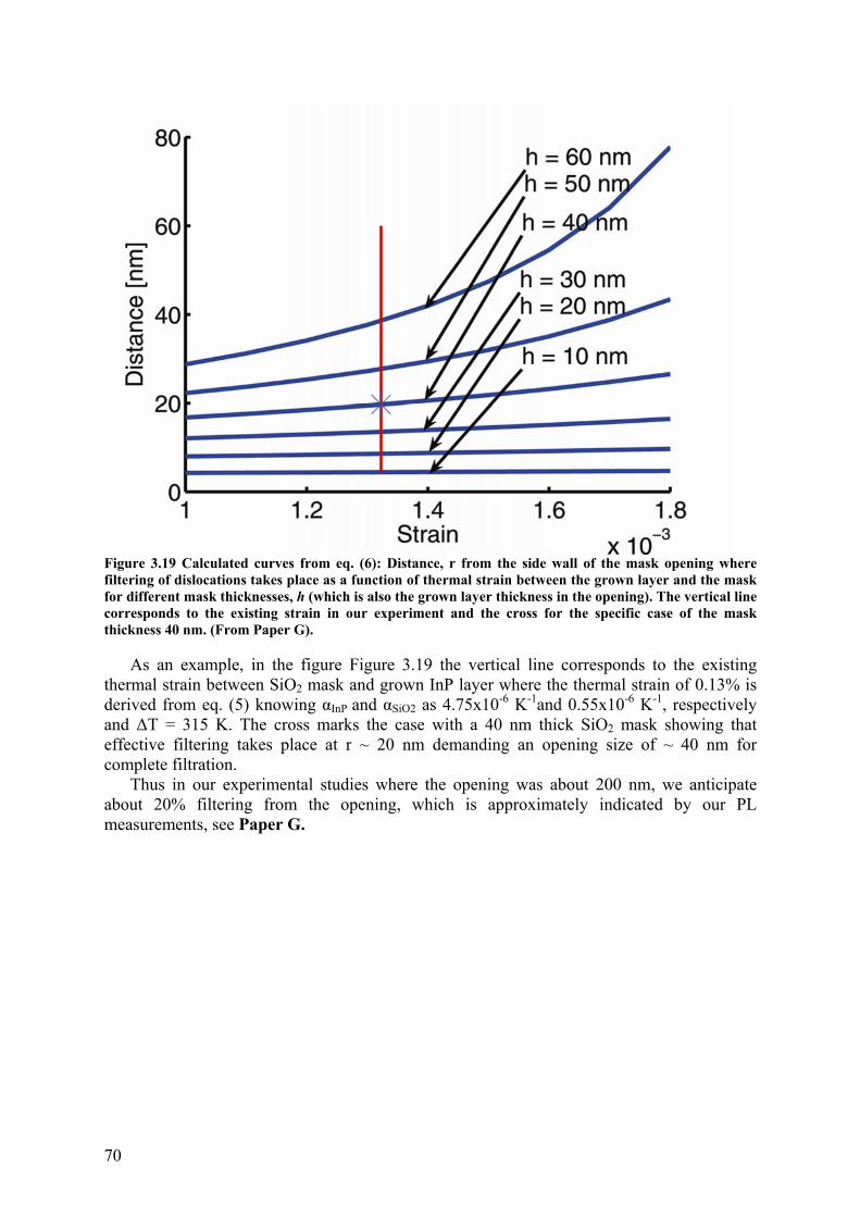
Figure 3.19 Calculated curves from eq. (6): Distance, r from the side wall of the mask opening where filtering of dislocations takes place as a function of thermal strain between the grown layer and the mask for different mask thicknesses, h (which is also the grown layer thickness in the opening). The vertical line corresponds to the existing strain in our experiment and the cross for the specific case of the mask thickness 40 nm. (From Paper G).
As an example, in the figure Figure 3.19 the vertical line corresponds to the existing thermal strain between SiO2 mask and grown InP layer where the thermal strain of 0.13% is derived from eq. (5) knowing αInP and αSiO2 as 4.75x10⁻⁶ K-1and 0.55x10⁻⁶ K-1, respectively and ΔT = 315 K. The cross marks the case with a 40 nm thick SiO2 mask showing that effective filtering takes place at r ~ 20 nm demanding an opening size of ~ 40 nm for complete filtration.
Thus in our experimental studies where the opening was about 200 nm, we anticipate about 20% filtering from the opening, which is approximately indicated by our PL measurements, see Paper G.
70
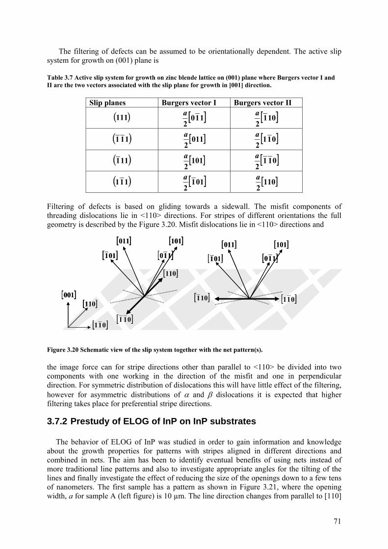
The filtering of defects can be assumed to be orientationally dependent. The active slip system for growth on (001) plane is Table 3.7 Active slip system for growth on zinc blende lattice on (001) plane where Burgers vector I and II are the two vectors associated with the slip plane for growth in [001] direction.
Slip planes Burgers vector I Burgers vector II
( )111 [ ]1102a
[ ]1012a
( )111 [ ]0112a
[ ]0112a
[ ]0112a
( )111 [ ]1012a
( )111 [ ]0112a
[ ]1102a
Filtering of defects is based on gliding towards a sidewall. The misfit components of threading dislocations lie in <110> directions. For stripes of different orientations the full geometry is described by the Figure 3.20. Misfit dislocations lie in <110> directions and Figure 3.20 Schematic view of the slip system together with the net pattern(s).
[ ]110
[ ]011
[ ]001
[ ]011
[ ]110
[ ]011
[ ]101
[ ]011
[ ]011[ ]101
[ ]011 [ ]101
[ ]011[ ]110 [ ]110
[ ]110
[ ]011
[ ]001
[ ]011
[ ]110
[ ]011
[ ]101
[ ]011
[ ]011[ ]101
[ ]011 [ ]101
[ ]011[ ]110 [ ]110
the image force can for stripe directions other than parallel to <110> be divided into two components with one working in the direction of the misfit and one in perpendicular direction. For symmetric distribution of dislocations this will have little effect of the filtering, however for asymmetric distributions of α and β dislocations it is expected that higher filtering takes place for preferential stripe directions.
3.7.2 Prestudy of ELOG of InP on InP substrates The behavior of ELOG of InP was studied in order to gain information and knowledge about the growth properties for patterns with stripes aligned in different directions and combined in nets. The aim has been to identify eventual benefits of using nets instead of more traditional line patterns and also to investigate appropriate angles for the tilting of the lines and finally investigate the effect of reducing the size of the openings down to a few tens of nanometers. The first sample has a pattern as shown in Figure 3.21, where the opening width, a for sample A (left figure) is 10 µm. The line direction changes from parallel to [110]
71
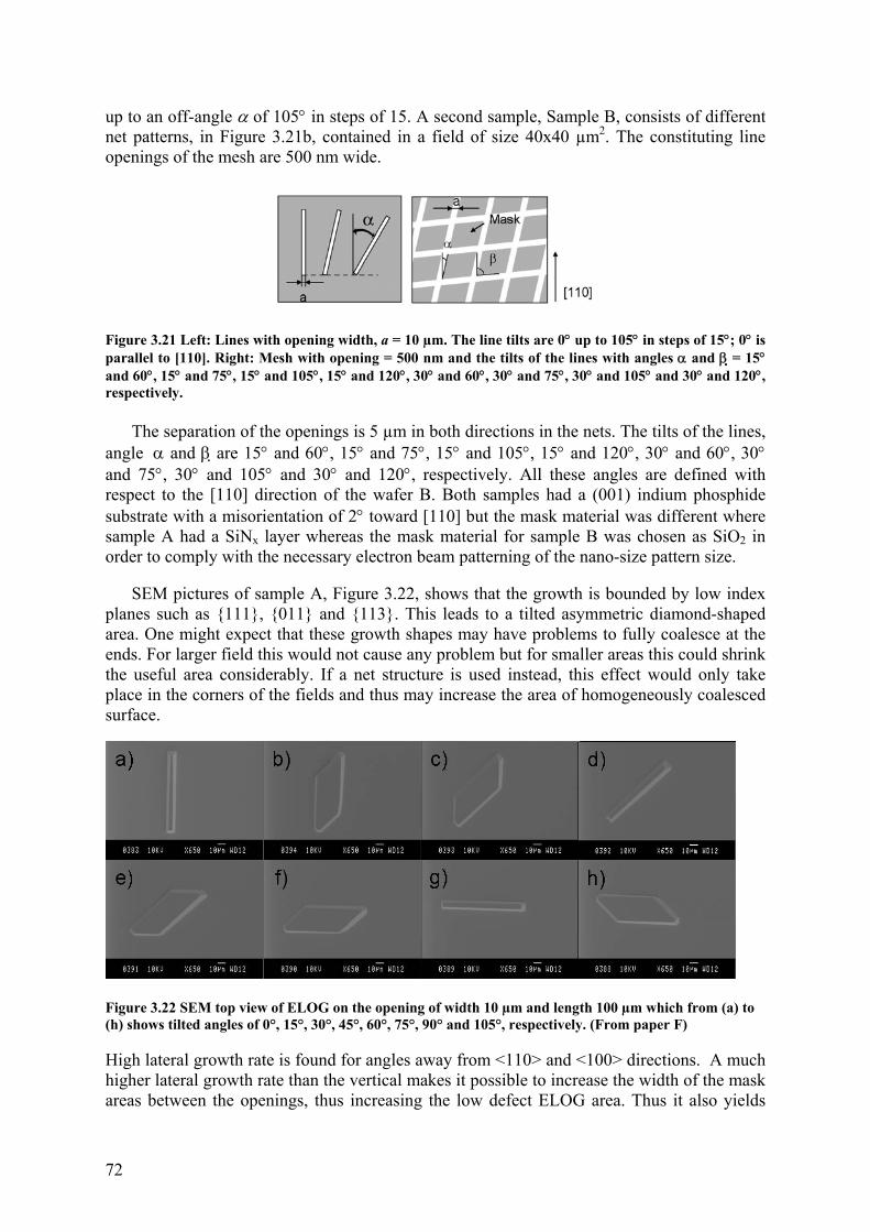
up to an off-angle α of 105° in steps of 15. A second sample, Sample B, consists of different net patterns, in Figure 3.21b, contained in a field of size 40x40 µm2. The constituting line openings of the mesh are 500 nm wide.
Figure 3.21 Left: Lines with opening width, a = 10 µm. The line tilts are 0° up to 105° in steps of 15°; 0° is parallel to [110]. Right: Mesh with opening = 500 nm and the tilts of the lines with angles α and β = 15° and 60°, 15° and 75°, 15° and 105°, 15° and 120°, 30° and 60°, 30° and 75°, 30° and 105° and 30° and 120°, respectively.
The separation of the openings is 5 µm in both directions in the nets. The tilts of the lines, angle α and β are 15° and 60°, 15° and 75°, 15° and 105°, 15° and 120°, 30° and 60°, 30° and 75°, 30° and 105° and 30° and 120°, respectively. All these angles are defined with respect to the [110] direction of the wafer B. Both samples had a (001) indium phosphide substrate with a misorientation of 2° toward [110] but the mask material was different where sample A had a SiNx layer whereas the mask material for sample B was chosen as SiO2 in order to comply with the necessary electron beam patterning of the nano-size pattern size.
SEM pictures of sample A, Figure 3.22, shows that the growth is bounded by low index planes such as {111}, {011} and {113}. This leads to a tilted asymmetric diamond-shaped area. One might expect that these growth shapes may have problems to fully coalesce at the ends. For larger field this would not cause any problem but for smaller areas this could shrink the useful area considerably. If a net structure is used instead, this effect would only take place in the corners of the fields and thus may increase the area of homogeneously coalesced surface.
Figure 3.22 SEM top view of ELOG on the opening of width 10 µm and length 100 µm which from (a) to (h) shows tilted angles of 0°, 15°, 30°, 45°, 60°, 75°, 90° and 105°, respectively. (From paper F) High lateral growth rate is found for angles away from <110> and <100> directions. A much higher lateral growth rate than the vertical makes it possible to increase the width of the mask areas between the openings, thus increasing the low defect ELOG area. Thus it also yields
72
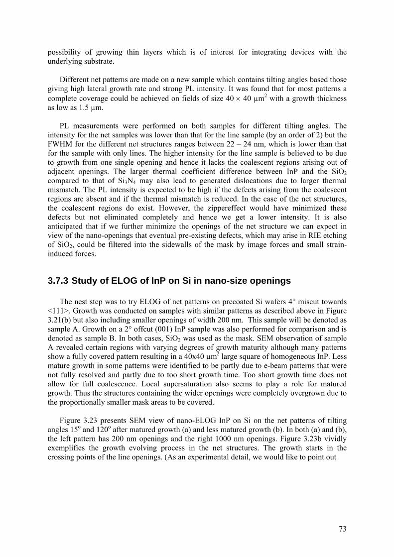
possibility of growing thin layers which is of interest for integrating devices with the underlying substrate. Different net patterns are made on a new sample which contains tilting angles based those giving high lateral growth rate and strong PL intensity. It was found that for most patterns a complete coverage could be achieved on fields of size 40 × 40 µm2 with a growth thickness as low as 1.5 µm. PL measurements were performed on both samples for different tilting angles. The intensity for the net samples was lower than that for the line sample (by an order of 2) but the FWHM for the different net structures ranges between 22 – 24 nm, which is lower than that for the sample with only lines. The higher intensity for the line sample is believed to be due to growth from one single opening and hence it lacks the coalescent regions arising out of adjacent openings. The larger thermal coefficient difference between InP and the SiO2 compared to that of Si3N4 may also lead to generated dislocations due to larger thermal mismatch. The PL intensity is expected to be high if the defects arising from the coalescent regions are absent and if the thermal mismatch is reduced. In the case of the net structures, the coalescent regions do exist. However, the zippereffect would have minimized these defects but not eliminated completely and hence we get a lower intensity. It is also anticipated that if we further minimize the openings of the net structure we can expect in view of the nano-openings that eventual pre-existing defects, which may arise in RIE etching of SiO2, could be filtered into the sidewalls of the mask by image forces and small strain-induced forces.
3.7.3 Study of ELOG of InP on Si in nano-size openings
The nest step was to try ELOG of net patterns on precoated Si wafers 4° miscut towards <111>. Growth was conducted on samples with similar patterns as described above in Figure 3.21(b) but also including smaller openings of width 200 nm. This sample will be denoted as sample A. Growth on a 2° offcut (001) InP sample was also performed for comparison and is denoted as sample B. In both cases, SiO2 was used as the mask. SEM observation of sample A revealed certain regions with varying degrees of growth maturity although many patterns show a fully covered pattern resulting in a 40x40 µm2 large square of homogeneous InP. Less mature growth in some patterns were identified to be partly due to e-beam patterns that were not fully resolved and partly due to too short growth time. Too short growth time does not allow for full coalescence. Local supersaturation also seems to play a role for matured growth. Thus the structures containing the wider openings were completely overgrown due to the proportionally smaller mask areas to be covered.
Figure 3.23 presents SEM view of nano-ELOG InP on Si on the net patterns of tilting
angles 15o and 120o after matured growth (a) and less matured growth (b). In both (a) and (b), the left pattern has 200 nm openings and the right 1000 nm openings. Figure 3.23b vividly exemplifies the growth evolving process in the net structures. The growth starts in the crossing points of the line openings. (As an experimental detail, we would like to point out
73
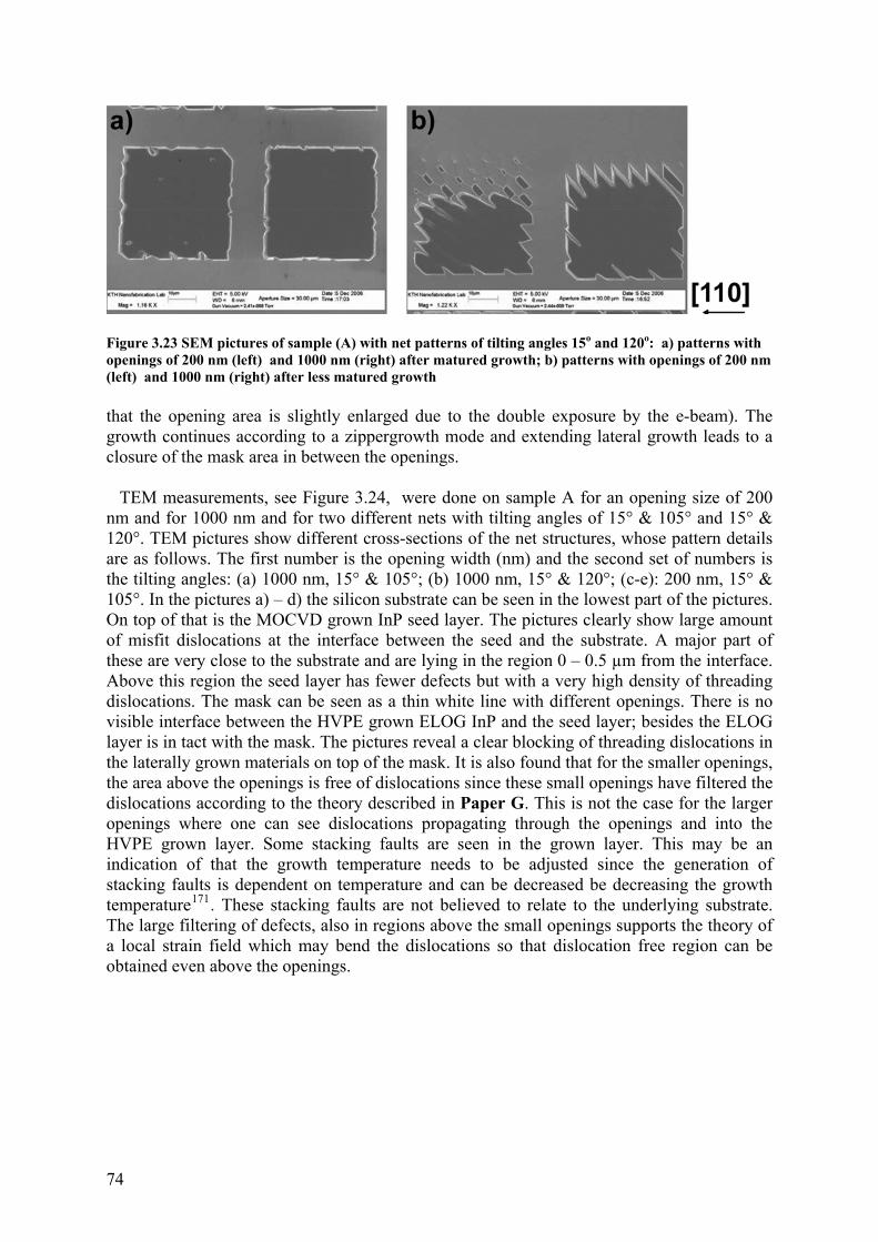
Figure 3.23 SEM pictures of sample (A) with net patterns of tilting angles 15o and 120o: a) patterns with openings of 200 nm (left) and 1000 nm (right) after matured growth; b) patterns with openings of 200 nm (left) and 1000 nm (right) after less matured growth that the opening area is slightly enlarged due to the double exposure by the e-beam). The growth continues according to a zippergrowth mode and extending lateral growth leads to a closure of the mask area in between the openings. TEM measurements, see Figure 3.24, were done on sample A for an opening size of 200 nm and for 1000 nm and for two different nets with tilting angles of 15° & 105° and 15° & 120°. TEM pictures show different cross-sections of the net structures, whose pattern details are as follows. The first number is the opening width (nm) and the second set of numbers is the tilting angles: (a) 1000 nm, 15° & 105°; (b) 1000 nm, 15° & 120°; (c-e): 200 nm, 15° & 105°. In the pictures a) – d) the silicon substrate can be seen in the lowest part of the pictures. On top of that is the MOCVD grown InP seed layer. The pictures clearly show large amount of misfit dislocations at the interface between the seed and the substrate. A major part of these are very close to the substrate and are lying in the region 0 – 0.5 µm from the interface. Above this region the seed layer has fewer defects but with a very high density of threading dislocations. The mask can be seen as a thin white line with different openings. There is no visible interface between the HVPE grown ELOG InP and the seed layer; besides the ELOG layer is in tact with the mask. The pictures reveal a clear blocking of threading dislocations in the laterally grown materials on top of the mask. It is also found that for the smaller openings, the area above the openings is free of dislocations since these small openings have filtered the dislocations according to the theory described in Paper G. This is not the case for the larger openings where one can see dislocations propagating through the openings and into the HVPE grown layer. Some stacking faults are seen in the grown layer. This may be an indication of that the growth temperature needs to be adjusted since the generation of stacking faults is dependent on temperature and can be decreased be decreasing the growth temperature171. These stacking faults are not believed to relate to the underlying substrate. The large filtering of defects, also in regions above the small openings supports the theory of a local strain field which may bend the dislocations so that dislocation free region can be obtained even above the openings.
74
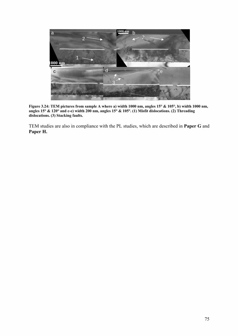
a b
c d e
2 2
3
1
Figure 3.24: TEM pictures from sample A where a) width 1000 nm, angles 15° & 105°, b) width 1000 nm, angles 15° & 120° and c-e) width 200 nm, angles 15° & 105°. (1) Misfit dislocations. (2) Threading dislocations. (3) Stacking faults. TEM studies are also in compliance with the PL studies, which are described in Paper G and Paper H.
75

76
4 Summary of appended papers Paper A Demonstration of Spectral Phase O-CDMA Encoding and Decoding in Monolithically Integrated Arrayed-Waveguide-Grating-Based Encoder Spectral phase encoding and decoding operation in a pair of monolithically integrated InP encoder chips, each consisting of an arrayed waveguide grating (AWG) pair and an eight-channel electrooptic phase shifter array are presented in this work. The monolithic fabrication process includes anisotropic reactive ion etching and planarizing hydride-vapor-phase-epitaxy lateral regrowth to realize buried hetero-waveguide structures in AWGs and phase shifters. Electrooptical modulation in the phase shifter arrays in the encoder chip achieved Walsh-code-based optical code-division multiple access (O-CDMA) encoding and decoding. The matched-code encoding–decoding operation resulted in error-free performance in the presence of an interferer, indicating good potential for O-CDMA network applications. Contribution: optimizing of regrowth, optimizing of deep etching conditions, taking part in fabricating/designing discussions. Paper B The Effect of Barrier Composition on the Vertical Carrier Transport and Lasing Properties of 1.55-µm Multiple Quantum-Well Structures In this paper, the effect of barrier bandgap and composition on the optical performance of 1.55- m InGaAsP/InGaAsP and InGaAsP/InGaAlAs multiple quantum-well structures and Fabry–Perot lasers is evaluated experimentally. Direct vertical carrier transport measurements were performed through strain-compensated multiple quantum-well (MQW) test structures using femto-second laser pulse excitation and time-resolved photoluminescence up-conversion method. MQW test structures were grown with different barrier composition (InGaAsP and InGaAlAs) and barrier bandgap (varied from λg = 1440 to1260 nm) having different conduction band ΔEc and valence band discontinuity ΔEv, while keeping the same InGaAsP well composition for all the structures. The ambipolar carrier transport was found to be faster in the structures with lower valence band discontinuity ΔEv . Regrown semi-insulating buried heterostructure Fabry–Perot (SIBH-FP) lasers were fabricated from similar QWs and their static light–current–voltage characteristics (including optical gain and chirp
77
spectra below threshold) and thermal characteristics were measured. Lasers with InGaAlAs barrier showed improved high-temperature operation, higher optical gain, higher differential gain, and lower chirp, making them suitable candidates for high-bandwidth directly modulated uncooled laser applications. Contribution: Optimizing regrowth, taking part in fabricating-related discussions. Paper C Large mask area effects in selective area growth In this paper we analyze for the first time selective area growth (SAG) of GaAs by MOVPE on dark field patterns, where the different masking features are dense and at the same time the openings are surrounded by very large mask area (larger than the openings) in all directions. The growth efficiency as a function of filling factors is analyzed using one- and two-dimensional filling factors. That the SAG efficiency cannot be greater than one is found to be true, if a two-dimensional filling factor is employed; this treatment involves three-dimensional transport of the growth rendering species. Finite element method has been used to derive the longitudinal thickness profile in the openings by considering the three-dimensional model. The derived longitudinal thickness profile is found to fit very well with the experimentally measured profile. The diffusion length of the growth rendering species is also extracted from the above profile. For comparison, light field patterns are also treated. Our analysis confirms many previous observations that SAG in the light field patterns can be sufficiently explained by the two-dimensional model. Contribution: Designing experiment, developed theory, analysis and interpretations, calculations, leading discussions and writing. Paper D Heteroepitaxy of InP on Silicon-on-Insulator for Optoelectronic Integration Epitaxial lateral overgrowth of InP was performed on patterned silicon-on-insulator (SOI) and compared with that on Si substrates in a low pressure hydride vapor phase epitaxy system. The InP was characterized by cathodoluminescence. No red shift of peak wavelength was detected for InP/SOI indicating a negligible thermal strain. Additional low energy peaks were found in some regions with a granular structure on the SOI template. A subsequent growth of an InGaAsP/InP MQW (multi quantum well) structure (λ ~ 1.5 μm) was grown on the SOI template and on a planar InP reference sample by metal-organic phase epitaxy. The MQW was characterized by room temperature photoluminescence. A red shift of 35 nm with respect to the reference sample was attributed to the selective-area effect causing thicker wells and/or an increased indium content. Although the PL intensity was weaker than that obtained for the reference, the FWHMs were comparable. Contribution: Designing experiment, ELOG growth of samples, analysis and interpretations, taking part and leading discussions and writing.
78
Paper E Crystal Defects and Strain of Epitaxial InP Layers Laterally Overgrown on Si Defects in epitaxial laterally overgrown (ELO) InP layers are examined by high-resolution X-ray diffraction and synchrotron X-ray back-reflection and transmission topography. X-ray diffraction maps produce information about the overall crystal quality of the epitaxial layers in the InP ELO sample. The topographs show small angle boundaries, and the associated dislocations are located at the boundaries between the crystallites; allowing for their relative tilt, the maximum value for this is 0.06°. No defects inside the crystallites can be seen in the topographs, except for a small bending of 0.04° at most, of the ELO lattice planes. The section topographs show deformed X-ray interference fringes resulting from the large strain of the silicon lattice below the seeding areas. Contribution: Optimization of ELOG growth. Paper F Epitaxial lateral overgrowth of InP in micro line and submicro mesh openings Towards achieving a large area of InP on silicon, a study of ELOG of InP on InP has been undertaken on lines with different orientations and with openings that are 100 gm long and 10 gm wide. This knowledge has been transposed on sub-micro mesh structures. By this method we have obtained 2 µm thick InP on a mesh patterned InP. The layer exhibits room temperature photoluminescence (PL) with a full width half maximum of 24 nm. We propose that this intensity can be increased if nano-sized openings are used. Contribution: Designing experiment, making ELOG growth, analysis and interpretations, calculations, leading discussions and writing. Paper G (Manuscript) Epitaxial lateral overgrowth of InP on Si from nano-openings - Theoretical and experimental indication for defect filtering throughout the grown layer We present a model for the filtration of dislocations inside the seed window in epitaxial lateral overgrowth (ELO). We found that when the additive effects of image and gliding forces exceed the defect line tension force, filtering can occur even in the openings. The model is applied to ELO of InP on Si where the opening size and the thermal stress arising due to the mask and the grown material are taken into account and analyzed. Further, we have also designed the mask patterns in net structures where the tilting angles of the openings in the nets are chosen in order to take advantage of the filtering in the openings more effectively and to minimise new defects due to coalescence in ELO. PL intensities of ELO InP on Si and on InP are compared and found to be in qualitative agreement with the model. Contribution: Designing experiment, making ELOG growth, developed theory, analysis and interpretations, calculations, leading discussions and writing.
79
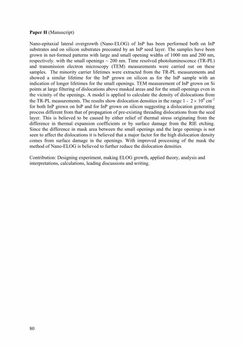
Paper H (Manuscript) Nano-epitaxial lateral overgrowth (Nano-ELOG) of InP has been performed both on InP substrates and on silicon substrates precoated by an InP seed layer. The samples have been grown in net-formed patterns with large and small opening widths of 1000 nm and 200 nm, respectively. with the small openings ~ 200 nm. Time resolved photoluminescence (TR-PL) and transmission electron microscopy (TEM) measurements were carried out on these samples. The minority carrier lifetimes were extracted from the TR-PL measurements and showed a similar lifetime for the InP grown on silicon as for the InP sample with an indication of longer lifetimes for the small openings. TEM measurement of InP grown on Si points at large filtering of dislocations above masked areas and for the small openings even in the vicinity of the openings. A model is applied to calculate the density of dislocations from the TR-PL measurements. The results show dislocation densities in the range 1 - 2 × 108 cm-2 for both InP grown on InP and for InP grown on silicon suggesting a dislocation generating process different from that of propagation of pre-existing threading dislocations from the seed layer. This is believed to be caused by either relief of thermal stress originating from the difference in thermal expansion coefficients or by surface damage from the RIE etching. Since the difference in mask area between the small openings and the large openings is not seen to affect the dislocations it is believed that a major factor for the high dislocation density comes from surface damage in the openings. With improved processing of the mask the method of Nano-ELOG is believed to further reduce the dislocation densities Contribution: Designing experiment, making ELOG growth, applied theory, analysis and interpretations, calculations, leading discussions and writing.
80
5 Summary of results, conclusions and future outlook
This thesis has been focusing on selective epitaxy and heteroepitaxy of InP for monolithic integration. The main results, conclusions and future outlook are summarized below.
(i) Regrowth of InP around deeply etched arrayed waveguide gratings can be successfully made by HVPE. We identify from the varying distance between the waveguide mesas as well as different crystallographic directions, there is a tendency for void formation due to the emergence of high index (hkl) planes but only for certain crystallographic directions. These high index planes readily propagate faster than (001) growth from the bottom. As a result these planes propagating from the adjacent mesas combinely lead to a closure with a resulting hole preferentially situated in the middle of the mesas at the bottom and bounded by (h11)B planes. The angular region where the void formation is taking place has been found to be dependent on local variation in the supersaturation and was found to arise for the waveguides lying at about 7° - 25° to about 12° - 19° away from [110] direction for 7 µm high and 4 µm high mesas, respectively. It was established that when designing patterns including waveguides the formation of voids can be minimized by avoiding directions in angular areas 5° - 25° off [ ]011 . We would like to emphasize that the device measurements and simulations indicate that these voids being far away from the active region, do not have noticeable adverse effect on device performance. More analysis needs to be undertaken.
(ii) Encoder/Decoder device with the array waveguide grating as its core element has been
fabricated with HVPE regrowth of semi-isolating InP. The decoders/encoders contain dense waveguides in all crystal directions. The regrowth resulted in excellent planarization and smooth low-loss transmission spectrum. Bit-Error-rate back-to-back measurements, single-user and two user case (with one user acting as the interferer) were performed. Both the single user and two-user case demonstrated error-free operation. We would like to point out that this is the first time that the regrowth technology has been employed to achieve such a device.
(iii) A multi-quantum well buried heterostructure laser emitting at 1.55 µm, that makes use of
AlGaInAs and InGaAsP as the barrier and well, respectively has been fabricated A combination of pre-growth cleaning with ammonium hydroxide for oxide removal and
81
very short in-situ etching by HCl have been proven to give high quality interfaces with the mesa sidewall and regrown InP:Fe. The lasers demonstrate threshold as low as 115A/cm2/quantum well, an external quantum efficiency of 45% and a characteristic temperature of 78 K, all at 20 oC.
(iv) Large mask area effects are important in cases where openings are surrounded by large
areas of masks. We studied selective area growth of GaAs under such conditions. From the modeling on large mask area effects, their impact on the transport and kinetic properties has been established. Experimental growth efficiency is found to be in agreement with the theoretically predicted values. We could predict the growth rate profile in the openings from the model. We have also derived the diffusion length of the Ga bearing species and found to be ~100 µm. These studies conclude that the large mask area effects should be considered in cases like ELOG where these are common.
(v) ELOG of InP on silicon-on-insulator and the growth of a quantum well structure on it have been demonstrated for the first time. Results indicate that the quality of ELOG InP is not comparable with that obtained on silicon. We used an exact oriented substrates for SOI but 4° off-cut towards <111> for ELOG of InP on silicon. Optmized growth of InP on SOI is very attractive for integration of InP on Si/SiO2 waveguides.
(vi) HRXRD measurements combined with synchrotron x-ray radiation measurements on ELOG InP show large edge effects on mask and deeply strain induced areas in the silicon substrate caused by the thermal strain arising from the difference in thermal expansion coefficients among the silicon substrate, the mask material and InP. These studies throw some light on the need for optimization of mask materials in the future studies.
(vii) The combination of strain and the influence of image forces when reducing the opening dimensions in ELOG has been modeled. It is found to be very beneficial to reduce the openings down to ~100 nm where effective filtering of dislocations is predicted to take place even in vicinity of the openings. We call this process nano-ELOG. By combining the modeling results of nano-ELOG and of a pre-study of ELOG on pure InP, a novel net pattern design is invented and experimented for nano-ELOG of InP on Si. PL measurements together with transmission electron microscopy observations indicate beneficial effects of small size openings (200 nm) compared to 1000 nm openings.
(viii) Results from nano-ELOG of InP on Si when compared with nano-ELOG of InP on InP wafers show comparable results but both exhibit a decreased PL intensity when compared with that of InP grown on planar substrate. The results seem to indicate better results for nano-ELOG in line with the theoretical prediction. The decrease in intensity in general for ELOG growth with respect to the planar growth is not clearly understood, but may involve other dislocation generating process.
Here are some suggestions for future work both for selective epitaxy and for ELOG.
A For improved regrowth and performance of dense array waveguides it might be interesting to try mirrors in the corners. Mirrors alone in the corners have been demonstrated. We propose that by combining corner mirrors and waveguides specifically lying in <110> or <100> directions, regrowth behavior around these directions can be excellent and mass transport for these directions is expected to be very beneficial due to the stable sidewalls.
82

B An analysis of regrowth behavior in the region 0 – 10 µm from the free propagation region would be beneficial.
C We suggest ELOG experiments on SOI substrates with very thin oxides to benefit from the theoretical prediction on compliant substrates; dislocations are supposed to move towards the silicon-SiO2 interface instead of propagating up in the InP.
D Use a combination of masks with both silicon nitride and silicon dioxide to cause better compliance between the thermal coefficients at the interfaces and to be able to easily wet etch the last part (by making use of etching selectivity) and thereby reducing the surface damage.
E Establish the dislocation density in the seed layer for which the growth behavior is proportional to the dislocation density according to the BCF growth mode. Insert a high temperature annealing shortly after start of ELOG growth in order to filter the dislocations before continuation of the lateral growth. This might improve the stability of the growth fronts and facilitate the coalescence process.
83
References 1 J. Bardeen, and W. H. Brattain, “The transistor, a semi-conductor triode,” Phys. Rev., vol. 74, no. 2, pp. 230 (1948). 2 http://www.porticus.org/bell/belllabs_transistor.html 3 J. S. Kilby, “Miniaturized electronic circuits,” U.S. Patent 3 138 743, Jun. 23, 1964. 4 R. N. Noyce, “Semiconductor device-and-lead structure,” U.S. Patent 2 981 877, Apr. 25, 1961. 5 G. E . Moore, “Cramming more components onto integrated circuits,” Electronics, vol. 38, no. 8, pp.114 (1965). 6 R. J. Keyes and T. M. Quist, “Unpublished paper,” presented at the IRE Solid State Device Research Conf., Durham, NH, 1962. 7 R. J. Keyes and T. M. Quist, “Recombination radiation emitted by gallium arsenide,” Proc. IRE, vol. 50, pp. 1822, (1962). 8 R. N. Hall, G. E. Fenner, J. D. Kingsley, T. J. Soltys, and R. O. Carlson, “Coherent light emission from GaAs junctions,” Phys. Rev. Lett., vol. 9, pp. 366 (1962). 9 M. I. Nathan, W. P. Dumke, G. Burns, F. H. Dill Jr., and G. Lasher, “Stimulated emission of radiation from GaAs p-n junctions,” Appl. Phys. Lett., vol. 1, no.3, pp. 62 (1962). 10 N. Holonyak Jr., and S. F. Bevacqua, “Coherent (visible) light emission from Ga(As1–xPx) junctions,” Appl. Phys. Lett., vol. 1, no.4, pp. 82 (1962). 11 T. M. Quist, R. H. Rediker, R. J. Keyes, W. E. Krag, B. Lax, A. L. McWhorter, and H. J. Zeiger, “Semiconductor maser of GaAs,” Appl. Phys. Lett., vol. 1, no.4, pp. 91 (1962). 12 R. C. Alferness and A. Glass, “Bell labs technology trends and developments,” Bell Labs Tech. J., vol. 2, no. 2, pp. 1 (1988). 13 D. C. Gloge and I. Jacobs, Optical Fiber Telecommunications II, 1st ed. San Diego, CA: Academic, 1988, p. 857. 14 Nagarajan, R. et al., “Large Scale Photonic Integrated Circuits”, IEEE J. Sel. Topics Quantum Electron., 11, pp. 50 (2005). 15 B. Mason, J. Barton, G. A. Fish, L. A. Coldren, and S. P. DenBaars, “Design of sampled grating DBR lasers with integrated semiconductor optical amplifiers,” IEEE Photon. Technol. Lett., vol. 12, no. 7, pp. 762 (2000). 16 J.Chen, R.G. Broeke, Broeke, Y.Du, C. J.Cao, N.Chubun, P.Bjeletich, F.Olsson, S.Lourdudoss, R.Welty, C.Reinhardt, P.L.Stephan, S.J.B. Yoo, “Monolithically integrated InP-based photonic chip development for O-CDMA systems”, IEEE J Sel. Topics Quantum Electron., vol. 11, no. 1, pp. 66 (2005). 17 International Technology Roadmap for Semiconductors, 2005 Edition, available at http:www.itrs.net/. 18 D. J. Frank, “Power-constrained CMOS scaling limits,” IBM J. Res. Dev., vol. 46, no. 2/3, pp. 235 (2002). 19 D. Pham et al. , ”The design and implementation of a first-generation CELL processor,” IEEE Int. Solid-State Circuits Conf. Digest Techn. Papers 1, pp. 184–592 (2005). 20 K. Chang et al., “Clocking and circuit design for a parallel I/O on a first-generation CELL processor, “ IEEE Int. Solid-State Circuits Conf. Digest Techn. Papers 1, pp. 526–615 (2005) 21 M. Kobrinsky et al., “On-Chip Optical Interconnects,” Intel Technology J. vol. 8, no. 2, pp.129 (2004). 22 B. Jalali, “Making silicon lase,” Scientific American, vol. 296, no. 2, pp. 58 (2007). 23 B. Jalali, “Teaching silicon new tricks,” Nature Photon., vol. 1, no. 4, pp. 193 (2007). 24 S. G. Cloutier, P. A. Kossyrev, and J. Xu, “Optical gain and stimulated emission in periodic nanopatterned crystalline silicon,” Nature Mater., vol. 4, no. 12, pp. 887 (2005).
84
25 A. Irrera, D. Pacifici, M. Miritello, G. Franzo, F. Priolo, F. Iacona, D. Sanfilippo, G. Di Stefano, and P. G. Fallica, “Electroluminescence properties of light emitting devices based on silicon nanocrystals,” Physica E, vol. 16, no. 3-4, pp. 395 (2003). 26 L. Pavesi, L. Dal Negro, C. Mazzoleni, G. Franzò, and F. Priolo, “Optical gain in silicon nanocrystals”, Nature, vol. 408, no. 6811, pp. 440 (2000). 27 P.M. Fauchet, J. Ruan, H. Chen, L. Pavesi, L. Dal Negro, M. Cazzaneli, R.G. Elliman, N. Smith, M. Samoc, and B. Luther-Davies, “Optical gain in different silicon nanocrystal systems,” Opt. Mater., vol. 27, no. 5, pp. 745 (2005). 28 L. Pavesi, “Routes toward silicon-based lasers,” Mater. Today, vol. 8, no. 1, pp. 8 (2005). 29 O. Boyraz, and B. Jalali, “Demonstration of a silicon Raman laser,” Opt. Express., vol. 12, no. 12, pp. 5269 (2004). 30 H. Rong, R. Jones, A. Liu, O. Cohen, D. Hak, A. Fang, and M. Paniccia, “A continuous-wave Raman silicon laser,” Nature, vol. 433, no. 7027, pp. 725 (2005). 31 B. Jalali, “Can silicon change photonics?,” Phys. Stat. Sol. (a), vol. 205, no. 2, pp. 213 (2008) 32 T. Sasaki, H. Mori, M. Tachikawa, and T. Yamada, “Aging testes of InP-based laser diodes heteroepitaxially grown on Si substrates,” J. Appl. Phys., vol. 84, pp. 6725 (1998). 33 J.P. Van Derziel, and R.D. Dupuis, “Degradation of GaAs lasers and light-emitting diodes on silicon substrates,” Mater. Sci Eng. B., vol. 1, no.1, pp. 37 (1988). 34 P. Peroff and R.L. Hartman, “Defect structure introduced operation of heterojunctions GaAs laser,” Appl. Phys. Lett., vol. 23, pp. 469 (1973). 35 L. Di Cioccio, E. Jalaguier, and F. Letertre, “III-V layer transfer onto silicon and applications,” Phys. Stat. Sol. (a), vol. 202, no. 4, pp. 509 (2005). 36 Q. Y. Tong, and U. M. Gösele, “Wafer bonding and layer splitting for microsystems,” Adv. Mater., vol. 11, no. 17, pp. 1409 (1999). 37 C. Monat, C. Seassal, X. Letartre, P. Viktorovitch, P. Regreny,M. Gendry, P. Rojo-Romeo, G. Hollinger, E. Jalaguier, S. Pocas, and B. Aspar, “InP 2D photonic crystal microlasers on silicon wafer: Room temperature operation at 1.55 μm,” Electron. Lett., vol. 37, no. 12, pp. 764 (2001). 38 D. Pasquariello, and K. Hjort, “Plasma-assisted InP-to-Si low temperature wafer bonding,” IEEE J. Sel. Topics Quantum Electron., vol. 8, no. 1, pp. 118 (2002). 39 T. Akatsu, A. Plossl, R. Scholz, H. Stenzel, and U. Gosele, “Wafer bonding of different III–V compound semiconductors by atomic hydrogen surface cleaning,” J. Appl. Phys., vol. 90, no. 8, pp. 3856 (2001). 40 B. F. Levine, C. J. Pinzone, S. Hui, C. A. King, R. E. Leibenguth, D. R. Zolnowski, D. V. Lang, H. W. Krautter, and M. Geva, “Ultralow-dark-current wafer-bonded Si/InGaAs photodetectors,” Appl. Phys. Lett., vol. 75, no. 14, pp. 2141 (1999). 41 J. Brouckaert, G. Roelkens, D. van Thourhout, and R. Bates, “Thin-Film III-V Photodetectors Integrated on Silicon-on-Insulator Photonic ICs,” J. Light. Tech., vol. 25, no. 4, pp. 1053 (2007). 42 H. C. Lin, K. L. Chang, G. W. Pickrell, K. C. Hsieh, and K. Y. Cheng, “Low temperature wafer bonding by spin on glass,” J. Vac. Sci.Technol. B, vol. 20, no. 2, pp. 752 (2002). 43 W. P. Eaton, S. H. Risbud, and R. L. Smith, “Silicon wafer-to-wafer bonding at T<200 °C with polymethylmethacrylate,” Appl. Phys. Lett., vol. 65, no. 4, pp. 439 (1994). 44 G. Roelkens, J. Brouckaert, D. Taillaert, P. Dumon, W. Bogaerts, D. Van Thourhout, R. Baets, R. Nötzel, and M. Smit, “Integration of InP/InGaAsP photodetectors onto silicon-on-insulator waveguide circuits,” Opt. Express, vol. 13, no. 25, pp. 10102 (2005). 45 J.M. Fedeli, s. Jeannota, M. Kostrzewa, L. Di Cioccio, V. Jousseaume, R. Orobtchouk, P. Maury, M. Zussy, “Two different ways for waveguides and optoelectronics components on top of C-MOS,” Proceedings of SPIE - The International Society for Optical Engineering, v 6180, Photonics, Devices and Systems III (2006). 46 A. W. Fang, H. Park, R. Jones, O. Cohen, M. J. Paniccia, and J. E. Bowers, “A continuous-wave hybrid AlGaInAs-silicon evanescent laser,” IEEE Photon. Technol. Lett., vol. 18, no. 10, pp. 1143 (2006). 47 J. Arokiaraj, S. Vickesh, and A. Ramam, “Integration of Indium Phosphide Thin Film Structures on Silicon Substrates by Direct Wafer Bonding”, J. of Phys. Conf. Series, vol. 34, pp. 404 (2006). 48 H. Huang, X. Ren, W. Wang, H. Song, Q. Wang, S. Cai, and Y. Huang, “Low Temperature InP/Si wafer bonding using boride treated surface,” Appl. Phys. Lett., vol. 90, no. 16, pp. 161102 (2007) 49 J. E. Ayers, ”Heteroepitaxy of Semiconductors: Theory, Growth and Characterization,” CRC Press, Taylor & Francis Group (2007). 50 E. A. Fitzgerald, A. Y. Kim, M. T. Currie, T. A. Langdo, G. Tarischi, and M. T. Bulsara, “Dislocation dynamics in relaxed graded composition semiconductors,” Mater. Sci. Eng. B, vol. 67, no. 1-2, pp. 53 (1999). 51 A. Seki, F. Konushi, J. Kudo, and M. Kuba, “Epitaxial growth of InP on Si by OMVPE-defect reduction in epitaxial InP using InAsxP1-x/InP superlattices”, J. Cryst. Growth, vol. 93, no. 1-4, pp. 527 (1988).
85
52 T.E. Crumbaker, H.Y. Lee, M.J. Hafich, and G.Y. Robinson, “Growth of InP on Si substrates by molecular beam epitaxy”, App. Phys. Lett., vol. 54, no. 2, pp. 140 (1989). 53 K. Samonji, H. Yonezu, Y. Takagi, K. Iwaki, N. Ohshima, J.K. Shin, K. Pak, “Reduction of threading dislocation density in InP-on-Si heteroepitaxy with strained short-period superlattices,” App. Phys. Lett., vol. 69, no. 1, pp. 100 (1996). 54 R.F. Schnabel, L. Grundmann, A. Krost, J. Christen, F. Heinrichsdorff, D. Bimberg, and H. Cerva, “Defect reductions and strain relaxation mechanisms in InP grown on patterned Si(001)”, 6th International Conference on Indium Phosphide and Related Materials, pp. 640 (1994). 55 A. Bakin, D. Piester, I. Behrens, H.H. Wehmann, E. Peiner, A. Ivanov, D. Fehly, and A. Schlachetzki, “Growth of InP layers on nanometer-scale patterned Si substrates”, Crystal. Growth & Des., vol.3, no.1, pp. 89 (2003). 56 Y. Kohama, Y. Kadota, and Y. Ohmachi, “Heteroepitaxy of InP on Si substrates by MOCVD,” J. Elechem. Soc., vol. 136, no. 12, pp. 3853 (1989). 57 H. Mori, M. Sugo, and Y. Itoh, “Heteroepitaxy of InP on Si substrates”, Adv. Mater., vol. 5, no. 3, pp. 208 (1993). 58 M. Sugo, M. Yamaguchi, and M.M. Al-Jassim, “Heteroepitaxial growth of InP on Si substrates”, J. Cryst. Growth, vol. 99, no. 1-4, pp. 365 (1990). 59 M.K. Lee, D.S. Wuu, H.H. Tung, J.H. Chang, and Y.F. Lin, “Growth and characterization of InP epi-layers on ZnSe-coated Si substrates by low-pressure metalorganic vapor phase epitaxy”, Appl. Phys. Lett., vol. 53, pp. 107 (1988). 60 G. Saint-Girons, P. Regreny, L. Largeau, G. Patriarche, and G. Hollinger, “Monolithic integration of InP based heterostructures on Silicon using crystalline Gd2O3 buffers”, Appl. Phys. Lett., vol. 91, pp. 241912 (2007). 61 L. Jastrzebski, “SOI by CVD: epitaxial lateral overgrowth (ELO) process – review”, J. Cryst. Growth, vol. 63, p. 493 (1983). 62 R. W. McClelland, C. O. Bozler, and J. C. C. Fan, “A technique for producing epitaxial films on reusable substrates,” Appl. Phys. Lett., vol. 37, p. 560 (1980). 63 R. P. Gale, R. W. McClelland, J. C. C. Fan, and C. O. Bozler, “Lateral epitaxial overgrowth of GaAs by organometallic chemical vapor deposition”, Appl. Phys. Lett., vol. 41, no. 6, pp. 545 (1982). 64 P. Vohl, R. W. McClelland, C. O. Bozler, A. Chu, and A. J. Strauss, “Lateral growth of single-crystal InP over dielectric films by orientation-dependent VPE“, J. Cryst. Growth, vol. 56, p. 410 (1982). 65 B-Y. Tsaur, R.W. McClelland, J.C.C. Fan, R.P. Gale, J.P. Saöerno, B.A. Vojak, and C.O. Bozler, “Low-dislocation-density GaAs epi-layers grown on Ge-coated Si substrates by means of lateral epitaxial overgrowth”, Appl. Phy. Lett., vol. 41, no. 4, pp. 347 (1982). 66 S. Naritsuka and T. Nishinaga, “Epitaxial lateral overgrowth of InP by liquid phase epitaxy,” J. Cryst. Growth., vol. 146, no. 1-4, pp. 314 (1995). 67 Y. T. Sun, J. Napierala and S. Lourdudoss, “Selective area growth of InP on InP precoated silicon substrate by hydride vapor phase epitaxy’” 14th International Conference on Indium Phosphide and Related Materials, p. 339, IEEE, Stockholm, Sweden (2002). 68 M. Sugai, T. Kochiya, Y. Oyama, and J. Nishizawa, “Selective epitaxy of InP on Si(100) substrates prepared by liquid-phase epitaxy”, Jour. of Phys. and Chem. of Sol., vol. 69, no. 1-2, pp.411 (2008). 69 C. Kittel, Introduction to Solid State Physics 8th ed. John Wiley & Sons, New York, 2004. 70 B. Lee, S.S. Bose, M.H. Kim, A.D. Reed, G.E. Stillman, W.I. Wang, L. Vina, and P.C.Colter, “Orientation dependent amphoteric behavior of group IV impurities in the molecular beam epitaxial and vapor phase epitaxial growth of GaAs”, J. Cryst. Growth., vol. 96, no. 1 pp. 27 (1989). 71 D. Hull and D. J. Bacon, Introduction to dislocations, 4th ed., Butterworth Heinemann, Oxford, 2001, pp. 71. 72 D. W. Shaw, “Mechanisms in vapor phase epitaxy”, in Crystal growth C. H. L. Goodman, Ed. New York: Plenum, 1974, vol. 1, ch. 1. 73 B. Mutaftschiev, “Crystal growth and dislocations” in F. N. R. Nabarro (Ed.), Dislocation in Solids, Vol. 5, North-Holland, Amsterdam, (1980). 74 W. K. Burton, N. Cabrera and F. C. Frank, “The Growth of Crystals and the Equilibrium Structure of their Surfaces,” Philos. Trans. R. R. Soc. London, Ser. A, Mathematical and Physical Sciences, vol. 243, no. 866, pp. 299 (1951). 75 M. Kondo, C. Anayama, N. Okada, H. Sekiguchi, K. Domen, and T. Tanahashi, “Crystallographic orientation dependence of impurity incorporation into III-V compound semiconductors grown by metalorganic vapor phase epitaxy”, J. Appl. Phys., vol. 76, no. 2, pp. 914 (1994). 76 B. Lee, S.S. Bose, M.H. Kim, A.D. Reed, G.E. Stillman, W.I. Wang, L. Vina, and P.C. Colter, “Orientation dependent amphoteric behavior of group IV impurities in the molecular beam epitaxial and vapor phase epitaxial growth of GaAs”, J. Cryst. Growth, vol. 96, no. 1, pp. 27 (1989).
86
77 R. Bhat, C. Caneau, C.E. Zae, M.A. Koza, W.A. Bonner, D.M. Hwang, S.A. Schwarz, S.G. Menocal, and F.G. Favire, “Orientation dependence of S, Zn, Si, Te, and Sn doping in OMCVD growth of InP and GaAs: application to DH lasers and lateral p-n junction arrays grown on non-planar substrates”, J. Cryst. Growth, vol. 107, no.1-4, pp. 772 (1991). 78 Y. T. Sun, and S. Lourdudoss, “Sulfur doped indium phosphide on silicon substrate grown by epitaxial lateral overgrowth,” International Conference on Indium Phosphide and Related Materials 16 IPRM. Kagoshima, Japan, pp. 304 (2004).
th
79 E.F. Schubert, Doping in III-V Semiconductors, Cambridge Studies in Semiconductor Physics and Microelectronic Engineering, 1993. 80 O. Mizuno and H. Watanabe, “Semi-insulating properties of Fe-doped InP,” Electron. Lett., vol. 11, no.5, pp. 118 (1975).81 M.J. Harlow, W.J. Duncan, I.F. Lealman, and P.C. Spurdens, ”Chromium-doped semi-insulating InP grown by metalorganic vapour phase epitaxy,” J. Cryst. Growth, vol. 140, no.1-2, pp. 19 (1994). 82 C.D. Brandt, A.M. Hennel, L.M. Pawlovitcz, Y.-T Wu, T. Bryskiewicz, J. Lagowski, and H.C. Gatos, “New semi-insulating InP:Titanium midgap donors,” Appl. Phys. Lett., vol. 48, no. 17, pp. 1162 (1986). 83 A. Dadgar, O. Stenzel, L. Köhne, A. Näser, M. Strassburg, W. Stolz, D. Bimberg and H. Schumann, “Growth of Ru doped semi-insulating InP by low pressure metalorganic chemical vapor deposition,” J. Cryst. Growth, vol. 195, no. 1-4, pp. 69 (1998). 84 P. J. Corvini, ”Current Injection in Semi-Insulating Indium Phosphide”, Doctorlal Dissertation, ECE Technical Report No. 95-26, University of California, Santa Barbara (1995). 85 J.A. Long, V.G. Riggs, and W.D. Johnston, “Growth of Fe-doped semi-insulating InP by MOCVD,” J. Cryst. Growth vol. 69, no. 1, pp. 10 (1984). 86 S.Lourdudoss, B.Hammarlund and O.Kjebon, An Investigation on hydride VPE growth and properties of semi-insulating InP:Fe, J. Electron. Mater., vol. 19 no. 9, pp. 981 (1990). 87 F. Alexandre, O. Parillaud, D. C. Nguyen, R. Azoulay, M. Quillec, S. Bouchoule, G. Le Mestrellan, M. Juhel, G. Le Roux and E. V. K. Rao, “Low Temperature Planar regrowth of Semi-Insulating InP by Low Pressure Hydride Vapour Phase Epitaxy for Device Application”, J. Cryst. Growth, vol. 187, no. 3-4, pp. 347 (1998). 88 D. Söderström, S. Lourdudoss, A. Dadgar, O. Stnzel, D. Bimberg and H. Schumann, ”Dopant Diffusion and Current-Voltage Studies on Epitaxial InP codoped with Ru and Fe,” J. Electron. Mater., vol. 30, no. 8, pp. 972 (2001).89 M. Gibbon, J. P. Stagg, C. G. Cureton, E. J. Thrust, C. J. Jones, R. E. Mallard, R. E. Pritchards, N. Collis and A. Chew, “Selective-area low-pressure MOCVD of GaInAsP and related materials on planar InP substrates”, Semicond. Sci. Technol., vol. 8, no. 6, pp. 998 (1993). 90 M. Aoki, M. Suzuki, H. Sano, T. Kawano, T. Ido, T. Taniwatari, K. Uomi, A. Takai, IEEE J. Quantum Electron., ”InGaAs/InGaAsP MQW electroabsorption modulator integrated with a DFB laser fabricated by band-gap energy control selective area MOCVD,” vol. 29, no. 6, pp. 2088 (1993). 91 H. J. Oh, M. Sugiyama, Y. Nakano, Y. Shimogaki, “Surface Reaction Kinetics in Metalorganic Vapor Phase Epitaxy of GaAs through Analyses of Growth Rate Profile in Wide-Gap Selective-Area Growth,” Jpn. J. Appl. Phys., 42, 6284 (2003). 92 O. Kayser, “Selective growth of InP/GaInAs in LP-MOVPE and MOMBE/CBE”, J. Cryst. Growth, vol. 107, no. 1-4, pp. 989 (1991). 93 D. G. Coronell and K. F. Jensen, ”Analysis of MOCVD of GaAs on patterned substrates,” J. Cryst. Growth, vol. 114, no. 4, pp. 581 (1991). 94 M. E. Coltrin, C. C. Mitchell, “Mass transport and kinetic limitation in MOCVD selective-area growth,” J. Cryst. Growth., vol. 254, no. 1-2, pp. 35 (2003). 95 H. J. Queisser and E. E. Haller, “Defects in Semiconductors: some fatal, some vital,” Science, vol. 281, no. 5379, pp. 945 (1998). 96 M.E. Weiner, “Si contamination in open flow quartz systems for the growth of GaAs and GaP”, J. Electrochem. Soc., vol. 119, no. 4, pp. 496 (1972). 97 D. Jahan, D. Söderström, and S. Lourdudoss, “LP-HVPE growth of S, Fe and undoped InP”, 11th International Conference on Indium Phosphide and Related Materials, IEEE, Davos, Switzerland, pp. 123 (1999). 98 D. Hull and D. J. Bacon, Introduction to dislocations, 4th ed., Butterworth Heinemann, Oxford, 2001. 99 J. W. Matthews, S. Mader and T. B. Light, “Accommodation of misfit the interface between crystals of semiconducting elements or compounds,” J. Appl. Phys., vol. 41, no. 9, pp. 3800 (1970). 100 E. A. Fitzgerald, ”Dislocations in strained-layer epitaxy: theory, experiment, and applications,” Mat. Science Reports, vol. 7, no. 3, pp. 87 (1991). 101 D. Hull and D. J. Bacon, Introduction to dislocations, 4th ed., Butterworth Heinemann, Oxford, 2001, pp. 74 -80.
87
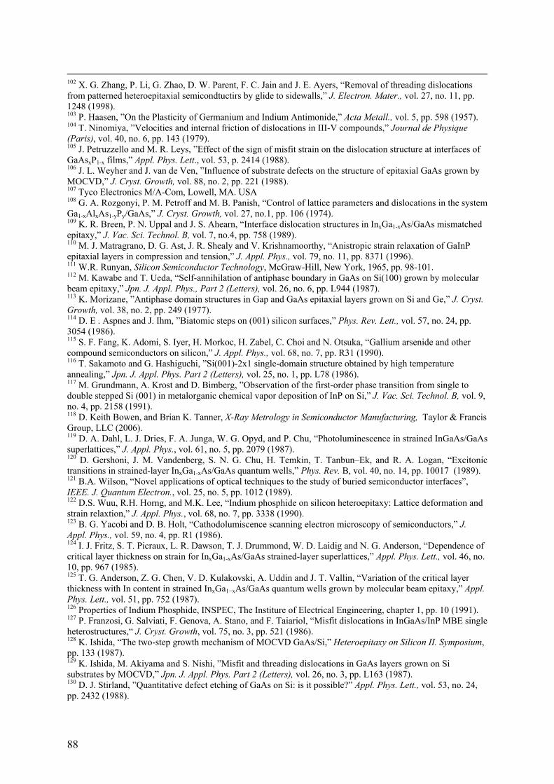
102 X. G. Zhang, P. Li, G. Zhao, D. W. Parent, F. C. Jain and J. E. Ayers, “Removal of threading dislocations from patterned heteroepitaxial semicondtuctirs by glide to sidewalls,” J. Electron. Mater., vol. 27, no. 11, pp. 1248 (1998). 103 P. Haasen, ”On the Plasticity of Germanium and Indium Antimonide,” Acta Metall., vol. 5, pp. 598 (1957). 104 T. Ninomiya, ”Velocities and internal friction of dislocations in III-V compounds,” Journal de Physique (Paris), vol. 40, no. 6, pp. 143 (1979). 105 J. Petruzzello and M. R. Leys, ”Effect of the sign of misfit strain on the dislocation structure at interfaces of GaAsxP1-x films,” Appl. Phys. Lett., vol. 53, p. 2414 (1988). 106 J. L. Weyher and J. van de Ven, ”Influence of substrate defects on the structure of epitaxial GaAs grown by MOCVD,” J. Cryst. Growth, vol. 88, no. 2, pp. 221 (1988). 107 Tyco Electronics M/A-Com, Lowell, MA. USA 108 G. A. Rozgonyi, P. M. Petroff and M. B. Panish, “Control of lattice parameters and dislocations in the system Ga1-xAlxAs1-yPy/GaAs,” J. Cryst. Growth, vol. 27, no.1, pp. 106 (1974). 109 K. R. Breen, P. N. Uppal and J. S. Ahearn, “Interface dislocation structures in InxGa1-xAs/GaAs mismatched epitaxy,” J. Vac. Sci. Technol. B, vol. 7, no.4, pp. 758 (1989). 110 M. J. Matragrano, D. G. Ast, J. R. Shealy and V. Krishnamoorthy, “Anistropic strain relaxation of GaInP epitaxial layers in compression and tension,” J. Appl. Phys., vol. 79, no. 11, pp. 8371 (1996). 111 W.R. Runyan, Silicon Semiconductor Technology, McGraw-Hill, New York, 1965, pp. 98-101. 112 M. Kawabe and T. Ueda, “Self-annihilation of antiphase boundary in GaAs on Si(100) grown by molecular beam epitaxy,” Jpn. J. Appl. Phys., Part 2 (Letters), vol. 26, no. 6, pp. L944 (1987). 113 K. Morizane, ”Antiphase domain structures in Gap and GaAs epitaxial layers grown on Si and Ge,” J. Cryst. Growth, vol. 38, no. 2, pp. 249 (1977). 114 D. E . Aspnes and J. Ihm, ”Biatomic steps on (001) silicon surfaces,” Phys. Rev. Lett., vol. 57, no. 24, pp. 3054 (1986). 115 S. F. Fang, K. Adomi, S. Iyer, H. Morkoc, H. Zabel, C. Choi and N. Otsuka, “Gallium arsenide and other compound semiconductors on silicon,” J. Appl. Phys., vol. 68, no. 7, pp. R31 (1990). 116 T. Sakamoto and G. Hashiguchi, ”Si(001)-2x1 single-domain structure obtained by high temperature annealing,” Jpn. J. Appl. Phys. Part 2 (Letters), vol. 25, no. 1, pp. L78 (1986). 117 M. Grundmann, A. Krost and D. Bimberg, ”Observation of the first-order phase transition from single to double stepped Si (001) in metalorganic chemical vapor deposition of InP on Si,” J. Vac. Sci. Technol. B, vol. 9, no. 4, pp. 2158 (1991). 118 D. Keith Bowen, and Brian K. Tanner, X-Ray Metrology in Semiconductor Manufacturing, Taylor & Francis Group, LLC (2006). 119 D. A. Dahl, L. J. Dries, F. A. Junga, W. G. Opyd, and P. Chu, “Photoluminescence in strained InGaAs/GaAs superlattices,” J. Appl. Phys., vol. 61, no. 5, pp. 2079 (1987). 120 D. Gershoni, J. M. Vandenberg, S. N. G. Chu, H. Temkin, T. Tanbun–Ek, and R. A. Logan, “Excitonic transitions in strained-layer InxGa1-xAs/GaAs quantum wells,” Phys. Rev. B, vol. 40, no. 14, pp. 10017 (1989). 121 B.A. Wilson, “Novel applications of optical techniques to the study of buried semiconductor interfaces”, IEEE. J. Quantum Electron., vol. 25, no. 5, pp. 1012 (1989). 122 D.S. Wuu, R.H. Horng, and M.K. Lee, “Indium phosphide on silicon heteroepitaxy: Lattice deformation and strain relaxtion,” J. Appl. Phys., vol. 68, no. 7, pp. 3338 (1990). 123 B. G. Yacobi and D. B. Holt, “Cathodolumiscence scanning electron microscopy of semiconductors,” J. Appl. Phys., vol. 59, no. 4, pp. R1 (1986). 124 I. J. Fritz, S. T. Picraux, L. R. Dawson, T. J. Drummond, W. D. Laidig and N. G. Anderson, “Dependence of critical layer thickness on strain for InxGa1-xAs/GaAs strained-layer superlattices,” Appl. Phys. Lett., vol. 46, no. 10, pp. 967 (1985). 125 T. G. Anderson, Z. G. Chen, V. D. Kulakovski, A. Uddin and J. T. Vallin, “Variation of the critical layer thickness with In content in strained InxGa1−xAs/GaAs quantum wells grown by molecular beam epitaxy,” Appl. Phys. Lett., vol. 51, pp. 752 (1987). 126 Properties of Indium Phosphide, INSPEC, The Institure of Electrical Engineering, chapter 1, pp. 10 (1991). 127 P. Franzosi, G. Salviati, F. Genova, A. Stano, and F. Taiariol, “Misfit dislocations in InGaAs/InP MBE single heterostructures,“ J. Cryst. Growth, vol. 75, no. 3, pp. 521 (1986).128 K. Ishida, “The two-step growth mechanism of MOCVD GaAs/Si,” Heteroepitaxy on Silicon II. Symposium, pp. 133 (1987). 129 K. Ishida, M. Akiyama and S. Nishi, ”Misfit and threading dislocations in GaAs layers grown on Si substrates by MOCVD,” Jpn. J. Appl. Phys. Part 2 (Letters), vol. 26, no. 3, pp. L163 (1987). 130 D. J. Stirland, ”Quantitative defect etching of GaAs on Si: is it possible?” Appl. Phys. Lett., vol. 53, no. 24, pp. 2432 (1988).
88
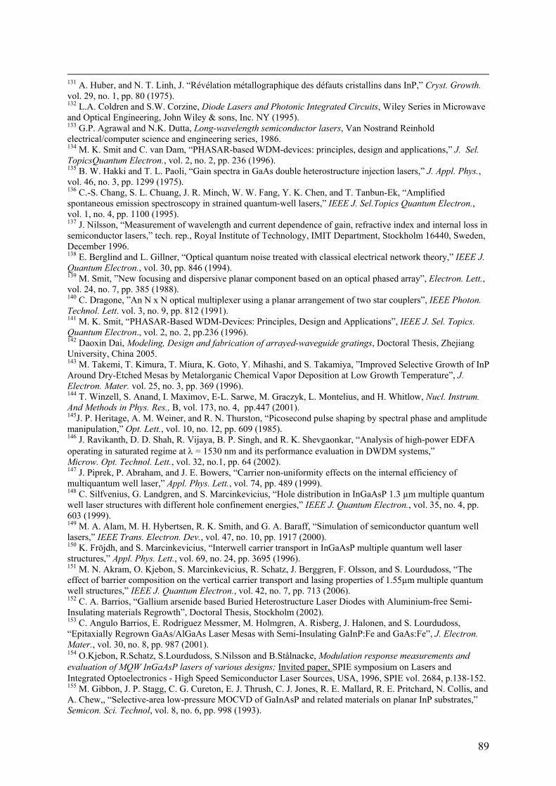
131 A. Huber, and N. T. Linh, J. “Révélation métallographique des défauts cristallins dans InP,” Cryst. Growth. vol. 29, no. 1, pp. 80 (1975). 132 L.A. Coldren and S.W. Corzine, Diode Lasers and Photonic Integrated Circuits, Wiley Series in Microwave and Optical Engineering, John Wiley & sons, Inc. NY (1995). 133 G.P. Agrawal and N.K. Dutta, Long-wavelength semiconductor lasers, Van Nostrand Reinhold electrical/computer science and engineering series, 1986. 134 M. K. Smit and C. van Dam, “PHASAR-based WDM-devices: principles, design and applications,” J. Sel. TopicsQuantum Electron., vol. 2, no. 2, pp. 236 (1996). 135 B. W. Hakki and T. L. Paoli, “Gain spectra in GaAs double heterostructure injection lasers,” J. Appl. Phys., vol. 46, no. 3, pp. 1299 (1975). 136 C.-S. Chang, S. L. Chuang, J. R. Minch, W. W. Fang, Y. K. Chen, and T. Tanbun-Ek, “Amplified spontaneous emission spectroscopy in strained quantum-well lasers,” IEEE J. Sel.Topics Quantum Electron., vol. 1, no. 4, pp. 1100 (1995). 137 J. Nilsson, “Measurement of wavelength and current dependence of gain, refractive index and internal loss in semiconductor lasers,” tech. rep., Royal Institute of Technology, IMIT Department, Stockholm 16440, Sweden, December 1996. 138 E. Berglind and L. Gillner, “Optical quantum noise treated with classical electrical network theory,” IEEE J. Quantum Electron., vol. 30, pp. 846 (1994). 139 M. Smit, ”New focusing and dispersive planar component based on an optical phased array”, Electron. Lett., vol. 24, no. 7, pp. 385 (1988). 140 C. Dragone, ”An N x N optical multiplexer using a planar arrangement of two star couplers”, IEEE Photon. Technol. Lett. vol. 3, no. 9, pp. 812 (1991). 141 M. K. Smit, “PHASAR-Based WDM-Devices: Principles, Design and Applications”, IEEE J. Sel. Topics. Quantum Electron., vol. 2, no. 2, pp.236 (1996). 142 Daoxin Dai, Modeling, Design and fabrication of arrayed-waveguide gratings, Doctoral Thesis, Zhejiang University, China 2005. 143 M. Takemi, T. Kimura, T. Miura, K. Goto, Y. Mihashi, and S. Takamiya, ”Improved Selective Growth of InP Around Dry-Etched Mesas by Metalorganic Chemical Vapor Deposition at Low Growth Temperature”, J. Electron. Mater. vol. 25, no. 3, pp. 369 (1996). 144 T. Winzell, S. Anand, I. Maximov, E-L. Sarwe, M. Graczyk, L. Montelius, and H. Whitlow, Nucl. Instrum. And Methods in Phys. Res., B, vol. 173, no. 4, pp.447 (2001). 145J. P. Heritage, A. M. Weiner, and R. N. Thurston, “Picosecond pulse shaping by spectral phase and amplitude manipulation,” Opt. Lett., vol. 10, no. 12, pp. 609 (1985). 146 J. Ravikanth, D. D. Shah, R. Vijaya, B. P. Singh, and R. K. Shevgaonkar, “Analysis of high-power EDFA operating in saturated regime at λ = 1530 nm and its performance evaluation in DWDM systems,” Microw. Opt. Technol. Lett., vol. 32, no.1, pp. 64 (2002). 147 J. Piprek, P. Abraham, and J. E. Bowers, “Carrier non-uniformity effects on the internal efficiency of multiquantum well laser,” Appl. Phys. Lett., vol. 74, pp. 489 (1999). 148 C. Silfvenius, G. Landgren, and S. Marcinkevicius, “Hole distribution in InGaAsP 1.3 µm multiple quantum well laser structures with different hole confinement energies,” IEEE J. Quantum Electron., vol. 35, no. 4, pp. 603 (1999). 149 M. A. Alam, M. H. Hybertsen, R. K. Smith, and G. A. Baraff, “Simulation of semiconductor quantum well lasers,” IEEE Trans. Electron. Dev., vol. 47, no. 10, pp. 1917 (2000). 150 K. Fröjdh, and S. Marcinkevicius, “Interwell carrier transport in InGaAsP multiple quantum well laser structures,” Appl. Phys. Lett., vol. 69, no. 24, pp. 3695 (1996). 151 M. N. Akram, O. Kjebon, S. Marcinkevicius, R. Schatz, J. Berggren, F. Olsson, and S. Lourdudoss, “The effect of barrier composition on the vertical carrier transport and lasing properties of 1.55µm multiple quantum well structures,” IEEE J. Quantum Electron., vol. 42, no. 7, pp. 713 (2006). 152 C. A. Barrios, “Gallium arsenide based Buried Heterostructure Laser Diodes with Aluminium-free Semi-Insulating materials Regrowth”, Doctoral Thesis, Stockholm (2002). 153 C. Angulo Barrios, E. Rodriguez Messmer, M. Holmgren, A. Risberg, J. Halonen, and S. Lourdudoss, “Epitaxially Regrown GaAs/AlGaAs Laser Mesas with Semi-Insulating GaInP:Fe and GaAs:Fe”, J. Electron. Mater., vol. 30, no. 8, pp. 987 (2001). 154 O.Kjebon, R.Schatz, S.Lourdudoss, S.Nilsson and B.Stålnacke, Modulation response measurements and evaluation of MQW InGaAsP lasers of various designs; Invited paper, SPIE symposium on Lasers and Integrated Optoelectronics - High Speed Semiconductor Laser Sources, USA, 1996, SPIE vol. 2684, p.138-152. 155 M. Gibbon, J. P. Stagg, C. G. Cureton, E. J. Thrush, C. J. Jones, R. E. Mallard, R. E. Pritchard, N. Collis, and A. Chew,, “Selective-area low-pressure MOCVD of GaInAsP and related materials on planar InP substrates,” Semicon. Sci. Technol, vol. 8, no. 6, pp. 998 (1993).
89
156 N. Hara, K. Shiina, T. Ohori, K. Kasai, and J. Komeno, “Lateral diffusion of sources during selective growth of Si-doped GaAs layers by metalorganic vapor phase epitaxy,” J. Appl. Phys., vol. 74, no.2, pp. 1327 (1993). 157 G. K. Cellar, and S. Cristoloveanu, “Frontiers of silicon-on-insulator,” J. Appl. Phys., vol. 93, no. 9, pp. 4955 (2003). 158 P. Dumon, W.Bogaerts, V. Wiaux, J. Wouters, S. Beckx, J. Van Campenhout, D. Taillaert, B. Luyssaert, P. Bienstman, D. Van Thourhout, and R.Baets, “Low-loss SOI photonic wires and ring resonators fabricated with deep UV lithography,” IEEE Photon. Technol. Lett., vol. 16, no. 5, pp. 1328 (2004). 159 Y. H. Lo, ”New approach to grow pseudomorphic structures grown over the critical layer thickness,” Appl. Phys. Lett., vol. 59, pp. 2311 (2005). 160 Z. Yang, F. Gaurin, I. W. Tao, W. I. Wang, and S. S. Iyer, “Approach to obtain high quality GaN on Si and SiC on silicon-on-insulator compliant substrates by molecular-beam epitaxy,” J. Vac. Sci. Technol. B, vol. 13, pp. 789 (1995). 161 C. Frigeri, R. Gleichmann, C. Pelosi, and G. Attolini, “Relationship between dislocation generation, vapour phase supersaturation and growth rate in InP layers obtained by vapour phase epitaxy,” Mater. Sci., vol. B10, no.3, pp. 197 (1991). 162 N. Duhamel, E.V.K. Rao, M. Gauneau, H. Thibierge, and A. Mircea, ”Silicon implantation in semi-insulating bulk InP; electrical and photoluminescence measurements,” J. Cryst. Growth, vol. 64, no.1, pp. 186 (1983). 163 D. E. Holmes, and G. S. Kamath, “Growth of InP by infinite solution LPE,” J. Cryst. Growth, vol. 54, no. 1, pp. 51 (1981). 164 R.A.Street, and R.H.Williams, “The luminescence of defects introduced by mechanical damage of InP,” J. Appl. Phys., vol. 52, no. 1, pp. 402 (1981).. 165 T. Kamijoh, H. Takano, and M. Sakuta, ”Heat treatment of semi-insulating InP:Fe with phosphosilicate glass encapsulation,” J. Appl. Phys., vol. 55, no.10, pp. 3756 (1984). 166 M.V. Rao, ”Photoluminescence study of the Si-implanted and rapid thermal annealed InP:Fe,” J. Appl. Phys. vol. 61, no. 1, pp. 337 (1987). 167 K. H. Chang, R. Gibala, D. J. Srolovitz, P. K. Bhattacharya, and J. F. Mansfield, “Crosshatched surface morphology in strained III-V semiconductor films,” J. Appl. Phys., vol. 67, no.9, pp. 4093 (1990). 168 Y. T. Sun, K. Baskar, and S. Lourdudoss, “Thermal strain in indium phosphide on silicon obtained by epitaxial lateral overgrowth,” J. Appl. Phys., vol. 94, no. 4, pp.2746 (2003). 169 Z. Yan, Y. Hamaoka, S. Naritsuka, and T. Nishinaga, “Coalescence in microchannel epitaxy of InP,” J. Cryst. Growth, vol.212, no. 1-2, pp. 1 (2000). 170 E. M. Rehder, C. K. Inoki, T. S. Kuan, and T. F. Kuech, “SiGe relaxation on silicon-on-insulator substrates: An experimental and modeling study,” J. Appl. Phys,. vol. 94, no. 12, pp. 7892 (2003). 171 M. Tachikawa, T. Yamada, T. Sasaki, H. Mori, and Y. Kadota,” Laser-Diode-Quality InP/Si Grown by Hydride Vapor Phase Epitaxy”, Jpn. J. Appl. Phys. Vol. 34. pp. L657 (1995).
90