Embed Size (px)
Citation preview
JLMN-Journal of Laser Micro/Nanoengineering Vol. 10, No. 3, 2015
274
Selective Femtosecond Laser Lift-off Process for Scribing in Thin-film Photovoltaics
Stephan KRAUSE*1, Paul-Tiberiu MICLEA*1,2 and Gerhard SEIFERT*1,3
*1 Fraunhofer Center for Silicon Photovoltaics CSP, Otto-Eißfeldt-Str. 12, 06120 Halle, Germany *2 Institute of Physics, Martin Luther University of Halle-Wittenberg, Heinrich-Damerow-Str. 4,
06120 Halle, Germany *3 Centre for Innovation Competence SiLi-nano®, Martin Luther University of Halle-Wittenberg,
Karl-Freiherr-von-Fritsch-Str. 3, 06120 Halle, Germany E-mail: [email protected]
A selective femtosecond laser lift-off process initiated by ultrafast non-thermal ablation of an ul-trathin layer at the interface of two materials has been explored with regard to its applicability in thin film photovoltaics. It is demonstrated that the technique allows preparing fully functional, i.e., electrically isolating, scribes of less than 20 µm groove width, leaving both groove bottom and lat-erally adjacent material without any indication of thermal damage or structural modification. The latter has been shown even for the textured interfaces of aluminium-doped zinc oxide (AZO) and silicon thin films. Laser wavelengths of 1030 nm and 515 nm were used for AZO and a-Si ablation, respectively. With this choice, sufficiently wide process windows of laser fluence could be identi-fied for all three typical scribes usually denoted as P1, P2 and P3 for patterning of front contact, ab-sorber and back contact. This shows that the femtosecond laser is a promising tool to reduce the to-tal width of the scribe areas in thin film solar modules to less than 50 µm. An additional benefit is the negligible thermal damage of the layers during scribing.
Keywords: thin films, photovoltaics, femtosecond lasers, laser scribes, lift-off process
1. Introduction Femtosecond laser processing is currently entering var-
ious new fields of application. Remarkable progress of commercially available fs laser systems with regard to per-formance, stability and reliability made them attractive for use in industrial production. While already established ap-plications like precise hole-drilling for fuel injectors, or structuring medical stents from tiny polymer tubes are more in the high price segment, the principal advantage of really ‘cold’ ablation due to interaction times below the time scale of electron–phonon coupling can be expected to be utilized for lower-price products soon.
In the field of photovoltaics, so far most of the estab-lished laser processes rely on cost effective and powerful nanosecond pulsed sources [1]. From a physical point of view, this is the best choice when thermal activation is re-quired like in the case of laser-fired contacts [2,3]. Other processes, however, like electrical structuring of individual layers for thin-film solar cells could clearly benefit from ultrashort laser pulse processing [4], for instance due to smaller heat affected zones, and less collateral damage by molten debris. Several authors have already demonstrated the advantages of picosecond processing for scribing of different thin film photovoltaic material systems [5-7]. The physical processes enabling selective induced ablation of thin layers [8] have been elucidated by detailed time-resolved investigations of thin absorbing metal films on transparent glass substrates [9]. Femtosecond pulses have been used, e.g., for direct ablation of transparent conduc-tive oxide (TCO) layers [10]. While this way of processing requires several pulses per spot to completely remove the
layer, femtosecond induced ablation works in single-shot mode, as has been demonstrated for the case of removing dielectric films from silicon wafers [11]. In this case, non-linear absorption and ultrafast vaporization of a 5-10 nm thin layer of the Si reduce the respective ablation threshold considerably (by approx. 30%) when pulses of 50 fs instead of ~2 ps pulse length are used [11]. As the interaction is governed by a very high electron density created by the fs pulse itself in the semiconductor adjacent to the interface SiO2/Si, a lift-off of the dielectric passivation layer without any damage to the opened silicon area is possible [12]. An analogous process enables lifting TCO layers from glass substrates by irradiation through the glass. The ablation thresholds observed for fs pulses at 1030 nm wavelength [13] of about 0.7 J/cm2 are more than a factor of 2 below those reported for 10 ps pulses at roughly the same wave-length [5].
In this work, we demonstrate the applicability of this highly selective femtosecond ablation process to all three ‘scribes’ normally required for the production of thin film solar cells (usually abbreviated as P1, P2 and P3 referring to patterning steps for front contact, absorber layer and back contact). It will be shown for the example of silicon thin film systems that the delamination and removal of in-dividual layers leaves the opened areas as well as the groove edges and adjacent regions of the remaining layers without any indication of damage or residual material.
2. Experimental
For the laser scribing experiments reported here, two different femtosecond laser systems have been used. The
DOI: 10.2961/jlmn.2015.03.0007
JLMN-Journal of Laser Micro/Nanoengineering Vol. 10, No. 3, 2015
275
first one was an Yb:KGW laser system (‘Pharos’ from Light Conversion Ltd.), which provides pulses of τ = 280 fs duration at a maximum repetition rate of ν = 350 kHz. The fundamental wavelength of 1030 nm (maximum average power 6W) and the second harmonic at 515 nm (max. ~ 3 W) have been used for lift-off processing. The second sys-tem is a Ti:Sapphire laser (‘Legend’ from Coherent Inc.) providing 120 fs pulses at 800 nm with ν = 1 kHz and an average power of 3.5 W. As processing setups an x-y-scanner system with f-theta lenses of 55 mm focal length (for λ = 1030 nm) or 100 mm (for λ = 515 nm), respective-ly, have been used in connection with the Pharos laser sys-tem. The Legend laser system was operated utilizing a fixed focusing lens (focal length 50 mm) together with a motorized x-y-stage for controlled sample movement. Pre-cise variation of the laser fluence was done using appropri-ate variable beam attenuators consisting of a suited half-wave plate and thin-film polarizer.
All lift-off experiments shown in this work have been conducted by irradiation through the glass substrate in an effective ‘single-shot’ ablation mode; this means that either the spot distance was chosen such that individual, circular craters were produced, or an effective spot-to-spot overlap of 60% (with respect to the 1/e2 diameter of the Gaussian beam waist) was used to create continuous grooves. The laser systems were operated with repetition frequencies of 50 kHz (Pharos) and 1 kHz (Legend), respectively.
Fig. 1 Schematic cross section of the different samples used in
this study. Several different samples have been used in this inves-
tigation. For the P1 scribes, two different types of TCO were ablated, namely an ITO (indium-doped tin oxide) layer of approx. 600 nm thickness, and for comparison an AZO (aluminium-doped zinc oxide) layer of approx. 1000 nm thickness, both on glass substrate with a thin buffer layer in between. These buffer layers (SiOx) with thick-nesses of 50 nm (ITO) and 100 nm (AZO) are highly trans-parent, electrically inactive and shall prevent sodium diffu-sion from glass into the TCOs. For the P2 and P3 scribes, a series of samples representing different stages of a tandem amorphous/microcrystalline silicon (a-Si/µc-Si) solar cell have been utilized; all samples are based on a soda-lime float glass sheet of ≈ 3 mm thickness, with the mentioned approximately 100 nm thick buffer layer between glass and TCO. The next stages are after deposition of a randomly textured AZO layer, followed by an approximately 300 nm thick a-Si layer, a µc-Si layer (approximately 800 nm thick), and finally an approximately 1000 nm thick ZnO back con-tact layer. Fig. 1 gives a sketch with schematic cross sec-
tions of all samples used. The relevant absorption coeffi-cient spectra of the samples are shown in Fig. 2
After scribe processing, the ablated grooves or craters have been analyzed optically with a Keyence Laser Scan-ning Microscope VK–X100. Additionally, cross section profiles were measured with an Ambios Technology pro-filometer XP-2. For an analysis on the nanoscale, scanning electron microscopy (SEM) images and energy dispersive X-ray (EDX) scans were acquired with a JEOL JSM-7401F electron microscope.
Fig. 2 Spectra of linear absorption coefficients of the two dif-
ferent (flat) TCOs and of an a-Si layer on (textured) AZO. Vertical arrows indicate the used fs-laser wavelengths.
3. Results and Discussion
Before we present new results, a brief summary will be given of the P1 scribing results of the flat ITO and AZO layers with fs laser pulses at 1030 nm wavelength, which have already been reported recently [13,14]. Though the AZO layer was thicker and had a lower (linear) absorption coefficient than ITO, the ablation thresholds Fth for both materials are nearly equal (≈0.5 J/cm2 for 600 nm thick ITO and ≈0.6 J/cm2 for 1000 nm thick AZO). The thresh-olds were determined from a plot of the square of the crater diameter versus logarithm of fluence, in analogy to previ-ous work [5,9,15]. Considering, in particular, that the thicker layer should require more energy for breaking the layer and ejection of the ‘disk’, the practically identical ablation thresholds provide a strong confirmation of the highly nonlinear character of the absorption and the result-ing lift-off process. The threshold for the AZO-buffer (≈0.9 J/cm2) is slightly larger than the AZO itself, while for ITO the buffer was removed along with it for all fluences over Fth(ITO). Diversity in thickness and doping-concentration at buffer/TCO interface are limiting the range for a selec-tive ablation of only TCO from the glass/buffer. Scribes conducted within a processing window from these thresh-olds up to the damage threshold of the glass at ≥ 3 J/cm2 yielded grooves with very smooth bottom and steep walls; an example (for ITO) is shown in the SEM image in Fig. 3.
JLMN-Journal of Laser Micro/Nanoengineering Vol. 10, No. 3, 2015
276
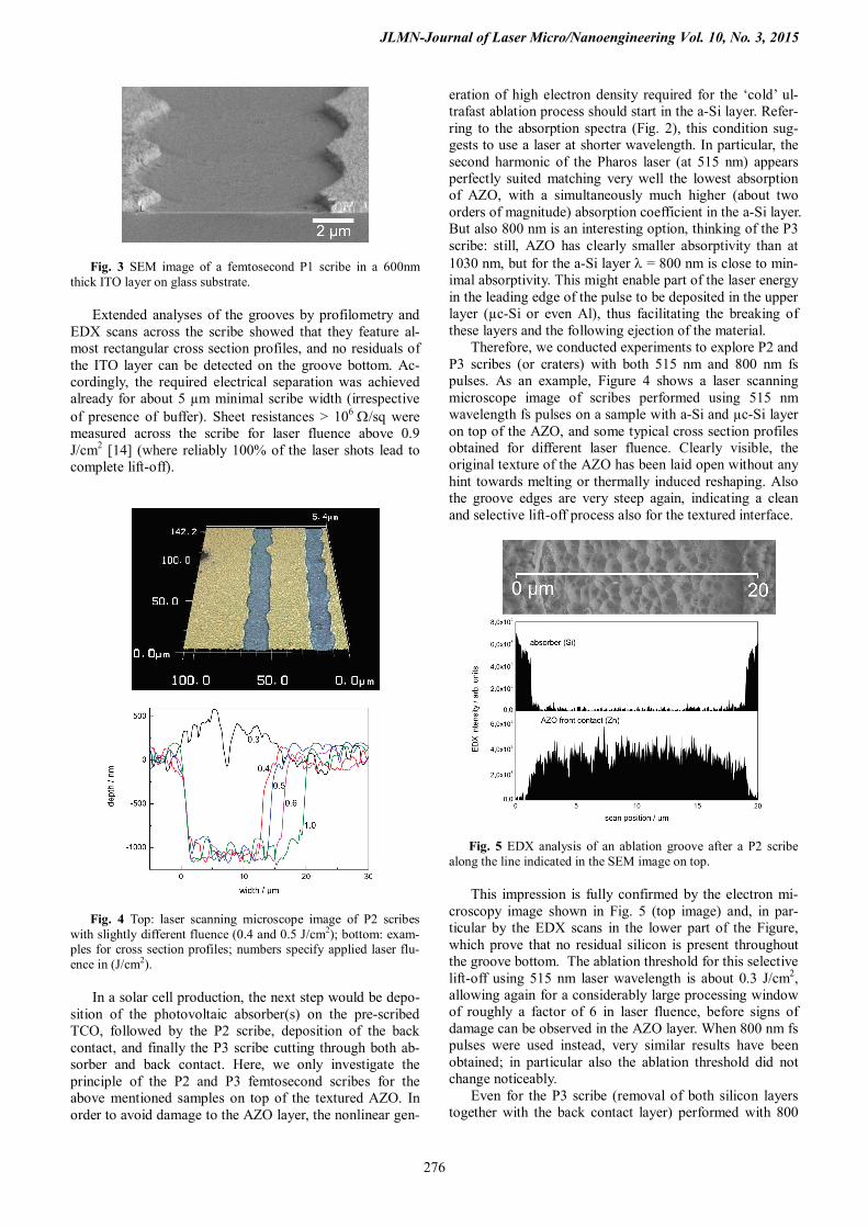
Fig. 3 SEM image of a femtosecond P1 scribe in a 600nm
thick ITO layer on glass substrate. Extended analyses of the grooves by profilometry and
EDX scans across the scribe showed that they feature al-most rectangular cross section profiles, and no residuals of the ITO layer can be detected on the groove bottom. Ac-cordingly, the required electrical separation was achieved already for about 5 µm minimal scribe width (irrespective of presence of buffer). Sheet resistances > 106 Ω/sq were measured across the scribe for laser fluence above 0.9 J/cm2 [14] (where reliably 100% of the laser shots lead to complete lift-off).
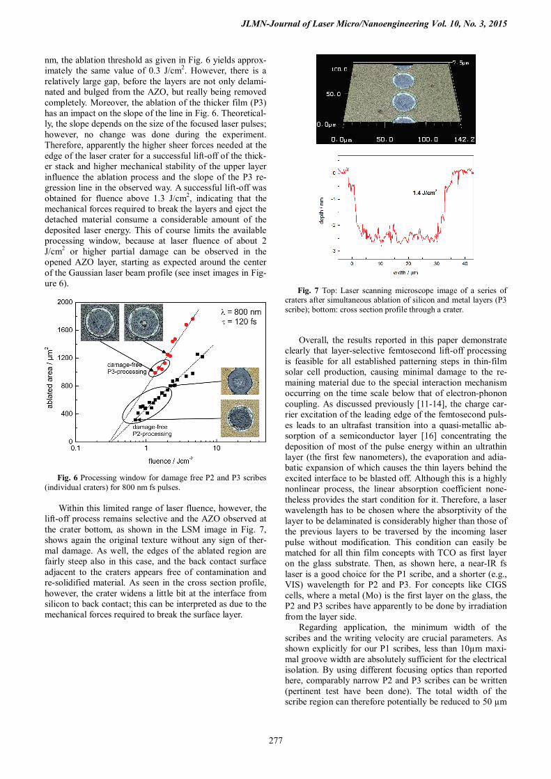
Fig. 4 Top: laser scanning microscope image of P2 scribes
with slightly different fluence (0.4 and 0.5 J/cm2); bottom: exam-ples for cross section profiles; numbers specify applied laser flu-ence in (J/cm2).
In a solar cell production, the next step would be depo-
sition of the photovoltaic absorber(s) on the pre-scribed TCO, followed by the P2 scribe, deposition of the back contact, and finally the P3 scribe cutting through both ab-sorber and back contact. Here, we only investigate the principle of the P2 and P3 femtosecond scribes for the above mentioned samples on top of the textured AZO. In order to avoid damage to the AZO layer, the nonlinear gen-
eration of high electron density required for the ‘cold’ ul-trafast ablation process should start in the a-Si layer. Refer-ring to the absorption spectra (Fig. 2), this condition sug-gests to use a laser at shorter wavelength. In particular, the second harmonic of the Pharos laser (at 515 nm) appears perfectly suited matching very well the lowest absorption of AZO, with a simultaneously much higher (about two orders of magnitude) absorption coefficient in the a-Si layer. But also 800 nm is an interesting option, thinking of the P3 scribe: still, AZO has clearly smaller absorptivity than at 1030 nm, but for the a-Si layer λ = 800 nm is close to min-imal absorptivity. This might enable part of the laser energy in the leading edge of the pulse to be deposited in the upper layer (µc-Si or even Al), thus facilitating the breaking of these layers and the following ejection of the material.
Therefore, we conducted experiments to explore P2 and P3 scribes (or craters) with both 515 nm and 800 nm fs pulses. As an example, Figure 4 shows a laser scanning microscope image of scribes performed using 515 nm wavelength fs pulses on a sample with a-Si and µc-Si layer on top of the AZO, and some typical cross section profiles obtained for different laser fluence. Clearly visible, the original texture of the AZO has been laid open without any hint towards melting or thermally induced reshaping. Also the groove edges are very steep again, indicating a clean and selective lift-off process also for the textured interface.
Fig. 5 EDX analysis of an ablation groove after a P2 scribe
along the line indicated in the SEM image on top. This impression is fully confirmed by the electron mi-
croscopy image shown in Fig. 5 (top image) and, in par-ticular by the EDX scans in the lower part of the Figure, which prove that no residual silicon is present throughout the groove bottom. The ablation threshold for this selective lift-off using 515 nm laser wavelength is about 0.3 J/cm2, allowing again for a considerably large processing window of roughly a factor of 6 in laser fluence, before signs of damage can be observed in the AZO layer. When 800 nm fs pulses were used instead, very similar results have been obtained; in particular also the ablation threshold did not change noticeably.
Even for the P3 scribe (removal of both silicon layers together with the back contact layer) performed with 800
JLMN-Journal of Laser Micro/Nanoengineering Vol. 10, No. 3, 2015
277
nm, the ablation threshold as given in Fig. 6 yields approx-imately the same value of 0.3 J/cm2. However, there is a relatively large gap, before the layers are not only delami-nated and bulged from the AZO, but really being removed completely. Moreover, the ablation of the thicker film (P3) has an impact on the slope of the line in Fig. 6. Theoretical-ly, the slope depends on the size of the focused laser pulses; however, no change was done during the experiment. Therefore, apparently the higher sheer forces needed at the edge of the laser crater for a successful lift-off of the thick-er stack and higher mechanical stability of the upper layer influence the ablation process and the slope of the P3 re-gression line in the observed way. A successful lift-off was obtained for fluence above 1.3 J/cm2, indicating that the mechanical forces required to break the layers and eject the detached material consume a considerable amount of the deposited laser energy. This of course limits the available processing window, because at laser fluence of about 2 J/cm2 or higher partial damage can be observed in the opened AZO layer, starting as expected around the center of the Gaussian laser beam profile (see inset images in Fig-ure 6).
Fig. 6 Processing window for damage free P2 and P3 scribes
(individual craters) for 800 nm fs pulses. Within this limited range of laser fluence, however, the
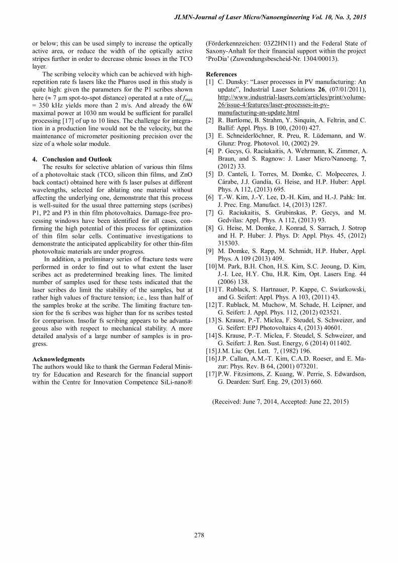
lift-off process remains selective and the AZO observed at the crater bottom, as shown in the LSM image in Fig. 7, shows again the original texture without any sign of ther-mal damage. As well, the edges of the ablated region are fairly steep also in this case, and the back contact surface adjacent to the craters appears free of contamination and re-solidified material. As seen in the cross section profile, however, the crater widens a little bit at the interface from silicon to back contact; this can be interpreted as due to the mechanical forces required to break the surface layer.
Fig. 7 Top: Laser scanning microscope image of a series of
craters after simultaneous ablation of silicon and metal layers (P3 scribe); bottom: cross section profile through a crater.
Overall, the results reported in this paper demonstrate
clearly that layer-selective femtosecond lift-off processing is feasible for all established patterning steps in thin-film solar cell production, causing minimal damage to the re-maining material due to the special interaction mechanism occurring on the time scale below that of electron-phonon coupling. As discussed previously [11-14], the charge car-rier excitation of the leading edge of the femtosecond puls-es leads to an ultrafast transition into a quasi-metallic ab-sorption of a semiconductor layer [16] concentrating the deposition of most of the pulse energy within an ultrathin layer (the first few nanometers), the evaporation and adia-batic expansion of which causes the thin layers behind the excited interface to be blasted off. Although this is a highly nonlinear process, the linear absorption coefficient none-theless provides the start condition for it. Therefore, a laser wavelength has to be chosen where the absorptivity of the layer to be delaminated is considerably higher than those of the previous layers to be traversed by the incoming laser pulse without modification. This condition can easily be matched for all thin film concepts with TCO as first layer on the glass substrate. Then, as shown here, a near-IR fs laser is a good choice for the P1 scribe, and a shorter (e.g., VIS) wavelength for P2 and P3. For concepts like CIGS cells, where a metal (Mo) is the first layer on the glass, the P2 and P3 scribes have apparently to be done by irradiation from the layer side.
Regarding application, the minimum width of the scribes and the writing velocity are crucial parameters. As shown explicitly for our P1 scribes, less than 10µm maxi-mal groove width are absolutely sufficient for the electrical isolation. By using different focusing optics than reported here, comparably narrow P2 and P3 scribes can be written (pertinent test have been done). The total width of the scribe region can therefore potentially be reduced to 50 µm
JLMN-Journal of Laser Micro/Nanoengineering Vol. 10, No. 3, 2015
278
or below; this can be used simply to increase the optically active area, or reduce the width of the optically active stripes further in order to decrease ohmic losses in the TCO layer.
The scribing velocity which can be achieved with high-repetition rate fs lasers like the Pharos used in this study is quite high: given the parameters for the P1 scribes shown here (≈ 7 µm spot-to-spot distance) operated at a rate of fmax = 350 kHz yields more than 2 m/s. And already the 6W maximal power at 1030 nm would be sufficient for parallel processing [17] of up to 10 lines. The challenge for integra-tion in a production line would not be the velocity, but the maintenance of micrometer positioning precision over the size of a whole solar module.
4. Conclusion and Outlook
The results for selective ablation of various thin films of a photovoltaic stack (TCO, silicon thin films, and ZnO back contact) obtained here with fs laser pulses at different wavelengths, selected for ablating one material without affecting the underlying one, demonstrate that this process is well-suited for the usual three patterning steps (scribes) P1, P2 and P3 in thin film photovoltaics. Damage-free pro-cessing windows have been identified for all cases, con-firming the high potential of this process for optimization of thin film solar cells. Continuative investigations to demonstrate the anticipated applicability for other thin-film photovoltaic materials are under progress.
In addition, a preliminary series of fracture tests were performed in order to find out to what extent the laser scribes act as predetermined breaking lines. The limited number of samples used for these tests indicated that the laser scribes do limit the stability of the samples, but at rather high values of fracture tension; i.e., less than half of the samples broke at the scribe. The limiting fracture ten-sion for the fs scribes was higher than for ns scribes tested for comparison. Insofar fs scribing appears to be advanta-geous also with respect to mechanical stability. A more detailed analysis of a large number of samples is in pro-gress.
Acknowledgments The authors would like to thank the German Federal Minis-try for Education and Research for the financial support within the Centre for Innovation Competence SiLi-nano®
(Förderkennzeichen: 03Z2HN11) and the Federal State of Saxony-Anhalt for their financial support within the project ‘ProDia’ (Zuwendungsbescheid-Nr. 1304/00013).
References [1] C. Dunsky: “Laser processes in PV manufacturing: An
update”, Industrial Laser Solutions 26, (07/01/2011), http://www.industrial-lasers.com/articles/print/volume-26/issue-4/features/laser-processes-in-pv-manufacturing-an-update.html
[2] R. Bartlome, B. Strahm, Y. Sinquin, A. Feltrin, and C. Ballif: Appl. Phys. B 100, (2010) 427.
[3] E. Schneiderlöchner, R. Preu, R. Lüdemann, and W. Glunz: Prog. Photovol. 10, (2002) 29.
[4] P. Gecys, G. Raciukaitis, A. Wehrmann, K. Zimmer, A. Braun, and S. Ragnow: J. Laser Micro/Nanoeng. 7, (2012) 33.
[5] D. Canteli, I. Torres, M. Domke, C. Molpeceres, J. Cárabe, J.J. Gandía, G. Heise, and H.P. Huber: Appl. Phys. A 112, (2013) 695.
[6] T.-W. Kim, J.-Y. Lee, D.-H. Kim, and H.-J. Pahk: Int. J. Prec. Eng. Manufact. 14, (2013) 1287.
[7] G. Raciukaitis, S. Grubinskas, P. Gecys, and M. Gedvilas: Appl. Phys. A 112, (2013) 93.
[8] G. Heise, M. Domke, J. Konrad, S. Sarrach, J. Sotrop and H. P. Huber: J. Phys. D: Appl. Phys. 45, (2012) 315303.
[9] M. Domke, S. Rapp, M. Schmidt, H.P. Huber, Appl. Phys. A 109 (2013) 409.
[10] M. Park, B.H. Chon, H.S. Kim, S.C. Jeoung, D. Kim, J.-I. Lee, H.Y. Chu, H.R. Kim, Opt. Lasers Eng. 44 (2006) 138.
[11] T. Rublack, S. Hartnauer, P. Kappe, C. Swiatkowski, and G. Seifert: Appl. Phys. A 103, (2011) 43.
[12] T. Rublack, M. Muchow, M. Schade, H. Leipner, and G. Seifert: J. Appl. Phys. 112, (2012) 023521.
[13] S. Krause, P.-T. Miclea, F. Steudel, S. Schweizer, and G. Seifert: EPJ Photovoltaics 4, (2013) 40601.
[14] S. Krause, P.-T. Miclea, F. Steudel, S. Schweizer, and G. Seifert: J. Ren. Sust. Energy, 6 (2014) 011402.
[15] J.M. Liu: Opt. Lett. 7, (1982) 196. [16] J.P. Callan, A.M.-T. Kim, C.A.D. Roeser, and E. Ma-
zur: Phys. Rev. B 64, (2001) 073201. [17] P.W. Fitzsimons, Z. Kuang, W. Perrie, S. Edwardson,
G. Dearden: Surf. Eng. 29, (2013) 660.
(Received: June 7, 2014, Accepted: June 22, 2015)